lp5951 micropower, 150ma low-dropout cmos voltage regulator · lp5951 micropower, 150ma low-dropout...
TRANSCRIPT
LP5951Micropower, 150mA Low-Dropout CMOS VoltageRegulatorGeneral DescriptionThe LP5951 regulator is designed to meet the requirementsof portable, battery-powered systems providing a regulatedoutput voltage and low quiescent current. When switched toshutdown mode via a logic signal at the Enable pin, thepower consumption is reduced to virtually zero.
The LP5951 is designed to be stable with small 1µF/1.5µFceramic capacitors.
The LP5951 also features internal protection against short-circuit currents and over-temperature conditions.
Performance is specified for a -40˚C to 125˚C temperaturerange.
The device is available in SOT23-5 and SC70-5 package.
The device is available in fixed output voltages in the rangeof 1.3V to 3.3V. For availability, please contact your localNSC sales office.
Featuresn Excellent line transient response: ±2mV typ.n Excellent PSRR: -60dB at 1kHz typ.n Low quiescent current of 29µA typ.n 1.8 to 5.5V input voltage rangen Small SC70-5 and SOT23-5 packagesn Fast turn-on time of 30µs typ.n Typ. < 1nA quiescent current in shutdownn Guaranteed 150mA output currentn Output voltage range: 1.3V to 3.3Vn Logic controlled enable 0.4V/0.9Vn Good load transient response of 50mVpp typ.n Thermal-overload and short-circuit protectionn -40˚C to +125˚C junction temperature range
Applicationsn General purpose
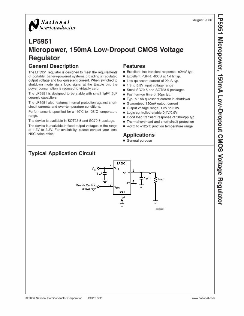
Typical Application Circuit
20136201
August 2006LP
5951M
icropower,150m
ALow
-Dropout
CM
OS
VoltageR
egulator
© 2006 National Semiconductor Corporation DS201362 www.national.com
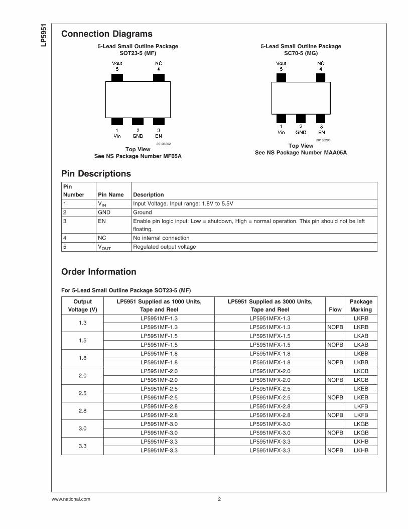
Connection Diagrams5-Lead Small Outline Package
SOT23-5 (MF)5-Lead Small Outline Package
SC70-5 (MG)
20136202
Top ViewSee NS Package Number MF05A
20136203
Top ViewSee NS Package Number MAA05A
Pin DescriptionsPinNumber Pin Name Description
1 VIN Input Voltage. Input range: 1.8V to 5.5V
2 GND Ground
3 EN Enable pin logic input: Low = shutdown, High = normal operation. This pin should not be leftfloating.
4 NC No internal connection
5 VOUT Regulated output voltage
Order Information
For 5-Lead Small Outline Package SOT23-5 (MF)
OutputVoltage (V)
LP5951 Supplied as 1000 Units,Tape and Reel
LP5951 Supplied as 3000 Units,Tape and Reel Flow
PackageMarking
1.3LP5951MF-1.3 LP5951MFX-1.3 LKRB
LP5951MF-1.3 LP5951MFX-1.3 NOPB LKRB
1.5LP5951MF-1.5 LP5951MFX-1.5 LKAB
LP5951MF-1.5 LP5951MFX-1.5 NOPB LKAB
1.8LP5951MF-1.8 LP5951MFX-1.8 LKBB
LP5951MF-1.8 LP5951MFX-1.8 NOPB LKBB
2.0LP5951MF-2.0 LP5951MFX-2.0 LKCB
LP5951MF-2.0 LP5951MFX-2.0 NOPB LKCB
2.5LP5951MF-2.5 LP5951MFX-2.5 LKEB
LP5951MF-2.5 LP5951MFX-2.5 NOPB LKEB
2.8LP5951MF-2.8 LP5951MFX-2.8 LKFB
LP5951MF-2.8 LP5951MFX-2.8 NOPB LKFB
3.0LP5951MF-3.0 LP5951MFX-3.0 LKGB
LP5951MF-3.0 LP5951MFX-3.0 NOPB LKGB
3.3LP5951MF-3.3 LP5951MFX-3.3 LKHB
LP5951MF-3.3 LP5951MFX-3.3 NOPB LKHB
LP59
51
www.national.com 2
Order Information (Continued)
For 5-Lead Small Outline Package SC70-5 (MG)
OutputVoltage (V)
LP5951 Supplied as 1000 Units,Tape and Reel
LP5951 Supplied as 3000 Units,Tape and Reel Flow
PackageMarking
1.3LP5951MG-1.3 LP5951MGX-1.3 L23
LP5951MG-1.3 LP5951MGX-1.3 NOPB L23
1.5LP5951MG-1.5 LP5951MGX-1.5 L2B
LP5951MG-1.5 LP5951MGX-1.5 NOPB L2B
1.8*LP5951MG-1.8 LP5951MGX-1.8 L3B
LP5951MG-1.8 LP5951MGX-1.8 NOPB L3B
2.0*LP5951MG-2.0 LP5951MGX-2.0 L4B
LP5951MG-2.0 LP5951MGX-2.0 NOPB L4B
2.5*LP5951MG-2.5 LP5951MGX-2.5 L5B
LP5951MG-2.5 LP5951MGX-2.5 NOPB L5B
2.8*LP5951MG-2.8 LP5951MGX-2.8 L6B
LP5951MG-2.8 LP5951MGX-2.8 NOPB L6B
3.0*LP5951MG-3.0 LP5951MGX-3.0 L7B
LP5951MG-3.0 LP5951MGX-3.0 NOPB L7B
3.3*LP5951MG-3.3 LP5951MGX-3.3 LAB
LP5951MG-3.3 LP5951MGX-3.3 NOPB LAB
* Not yet released. For availability please contact your local NSC sales office.
Note: The package marking on the backside of the component designates the date code and a NSC internal code for die traceability. It will vary considerably.
SOT23-5: ZWTT
SC70-5: WTT
with: Z: 1 Digit Assembly Plant Code, W: 1 Digit Date Code, TT: 2 Digit Dierun Code
LP5951
www.national.com3
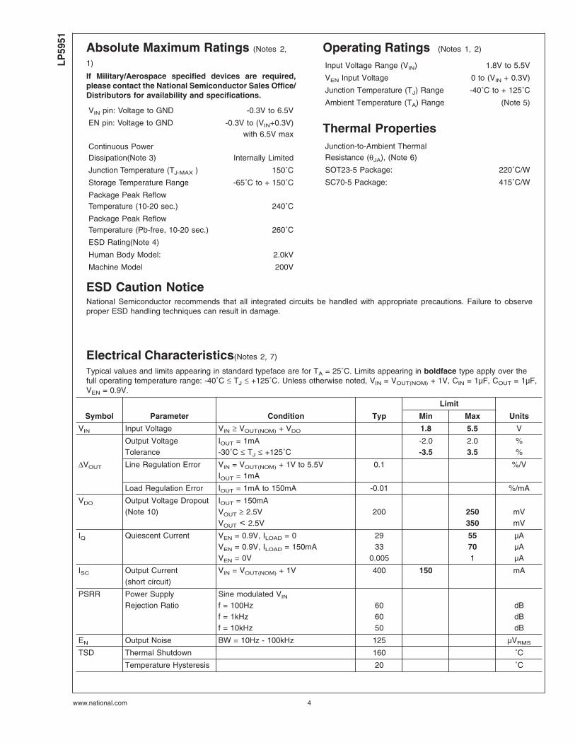
Absolute Maximum Ratings (Notes 2,
1)
If Military/Aerospace specified devices are required,please contact the National Semiconductor Sales Office/Distributors for availability and specifications.
VIN pin: Voltage to GND -0.3V to 6.5V
EN pin: Voltage to GND -0.3V to (VIN+0.3V)with 6.5V max
Continuous PowerDissipation(Note 3) Internally Limited
Junction Temperature (TJ-MAX ) 150˚C
Storage Temperature Range -65˚C to + 150˚C
Package Peak ReflowTemperature (10-20 sec.) 240˚C
Package Peak ReflowTemperature (Pb-free, 10-20 sec.) 260˚C
ESD Rating(Note 4)
Human Body Model: 2.0kV
Machine Model 200V
Operating Ratings (Notes 1, 2)
Input Voltage Range (VIN) 1.8V to 5.5V
VEN Input Voltage 0 to (VIN + 0.3V)
Junction Temperature (TJ) Range -40˚C to + 125˚C
Ambient Temperature (TA) Range (Note 5)
Thermal PropertiesJunction-to-Ambient ThermalResistance (θJA), (Note 6)
SOT23-5 Package: 220˚C/W
SC70-5 Package: 415˚C/W
ESD Caution NoticeNational Semiconductor recommends that all integrated circuits be handled with appropriate precautions. Failure to observeproper ESD handling techniques can result in damage.
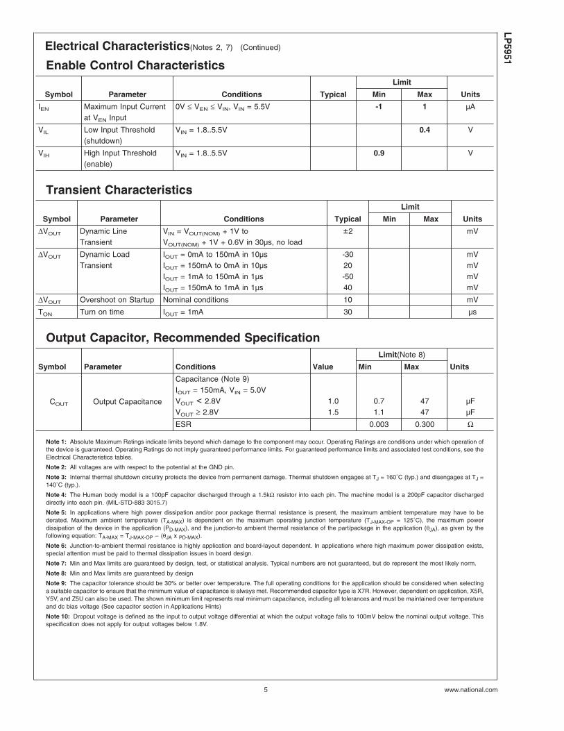
Electrical Characteristics(Notes 2, 7)
Typical values and limits appearing in standard typeface are for TA = 25˚C. Limits appearing in boldface type apply over thefull operating temperature range: -40˚C ≤ TJ ≤ +125˚C. Unless otherwise noted, VIN = VOUT(NOM) + 1V, CIN = 1µF, COUT = 1µF,VEN = 0.9V.
Symbol Parameter Condition Typ
Limit
UnitsMin Max
VIN Input Voltage VIN ≥ VOUT(NOM) + VDO 1.8 5.5 V
∆VOUT
Output VoltageTolerance
IOUT = 1mA-30˚C ≤ TJ ≤ +125˚C
-2.0-3.5
2.03.5
%%
Line Regulation Error VIN = VOUT(NOM) + 1V to 5.5VIOUT = 1mA
0.1 %/V
Load Regulation Error IOUT = 1mA to 150mA -0.01 %/mA
VDO Output Voltage Dropout(Note 10)
IOUT = 150mAVOUT ≥ 2.5VVOUT < 2.5V
200 250350
mVmV
IQ Quiescent Current VEN = 0.9V, ILOAD = 0VEN = 0.9V, ILOAD = 150mAVEN = 0V
2933
0.005
55701
µAµAµA
ISC Output Current(short circuit)
VIN = VOUT(NOM) + 1V 400 150 mA
PSRR Power SupplyRejection Ratio
Sine modulated VIN
f = 100Hzf = 1kHzf = 10kHz
606050
dBdBdB
EN Output Noise BW = 10Hz - 100kHz 125 µVRMS
TSD Thermal Shutdown 160 ˚C
Temperature Hysteresis 20 ˚C
LP59
51
www.national.com 4
Electrical Characteristics(Notes 2, 7) (Continued)
Enable Control Characteristics
Symbol Parameter Conditions Typical
Limit
UnitsMin Max
IEN Maximum Input Currentat VEN Input
0V ≤ VEN ≤ VIN, VIN = 5.5V -1 1 µA
VIL Low Input Threshold(shutdown)
VIN = 1.8..5.5V 0.4 V
VIH High Input Threshold(enable)
VIN = 1.8..5.5V 0.9 V
Transient Characteristics
Symbol Parameter Conditions Typical
Limit
UnitsMin Max
∆VOUT Dynamic LineTransient
VIN = VOUT(NOM) + 1V toVOUT(NOM) + 1V + 0.6V in 30µs, no load
±2 mV
∆VOUT Dynamic LoadTransient
IOUT = 0mA to 150mA in 10µsIOUT = 150mA to 0mA in 10µsIOUT = 1mA to 150mA in 1µsIOUT = 150mA to 1mA in 1µs
-3020-5040
mVmVmVmV
∆VOUT Overshoot on Startup Nominal conditions 10 mV
TON Turn on time IOUT = 1mA 30 µs
Output Capacitor, Recommended Specification
Symbol Parameter Conditions Value
Limit(Note 8)
UnitsMin Max
COUT Output Capacitance
Capacitance (Note 9)IOUT = 150mA, VIN = 5.0VVOUT < 2.8VVOUT ≥ 2.8V
1.01.5
0.71.1
4747
µFµF
ESR 0.003 0.300 Ω
Note 1: Absolute Maximum Ratings indicate limits beyond which damage to the component may occur. Operating Ratings are conditions under which operation ofthe device is guaranteed. Operating Ratings do not imply guaranteed performance limits. For guaranteed performance limits and associated test conditions, see theElectrical Characteristics tables.
Note 2: All voltages are with respect to the potential at the GND pin.
Note 3: Internal thermal shutdown circuitry protects the device from permanent damage. Thermal shutdown engages at TJ = 160˚C (typ.) and disengages at TJ =140˚C (typ.).
Note 4: The Human body model is a 100pF capacitor discharged through a 1.5kΩ resistor into each pin. The machine model is a 200pF capacitor dischargeddirectly into each pin. (MIL-STD-883 3015.7)
Note 5: In applications where high power dissipation and/or poor package thermal resistance is present, the maximum ambient temperature may have to bederated. Maximum ambient temperature (TA-MAX) is dependent on the maximum operating junction temperature (TJ-MAX-OP = 125˚C), the maximum powerdissipation of the device in the application (PD-MAX), and the junction-to ambient thermal resistance of the part/package in the application (θJA), as given by thefollowing equation: TA-MAX = TJ-MAX-OP – (θJA x PD-MAX).
Note 6: Junction-to-ambient thermal resistance is highly application and board-layout dependent. In applications where high maximum power dissipation exists,special attention must be paid to thermal dissipation issues in board design.
Note 7: Min and Max limits are guaranteed by design, test, or statistical analysis. Typical numbers are not guaranteed, but do represent the most likely norm.
Note 8: Min and Max limits are guaranteed by design
Note 9: The capacitor tolerance should be 30% or better over temperature. The full operating conditions for the application should be considered when selectinga suitable capacitor to ensure that the minimum value of capacitance is always met. Recommended capacitor type is X7R. However, dependent on application, X5R,Y5V, and Z5U can also be used. The shown minimum limit represents real minimum capacitance, including all tolerances and must be maintained over temperatureand dc bias voltage (See capacitor section in Applications Hints)
Note 10: Dropout voltage is defined as the input to output voltage differential at which the output voltage falls to 100mV below the nominal output voltage. Thisspecification does not apply for output voltages below 1.8V.
LP5951
www.national.com5
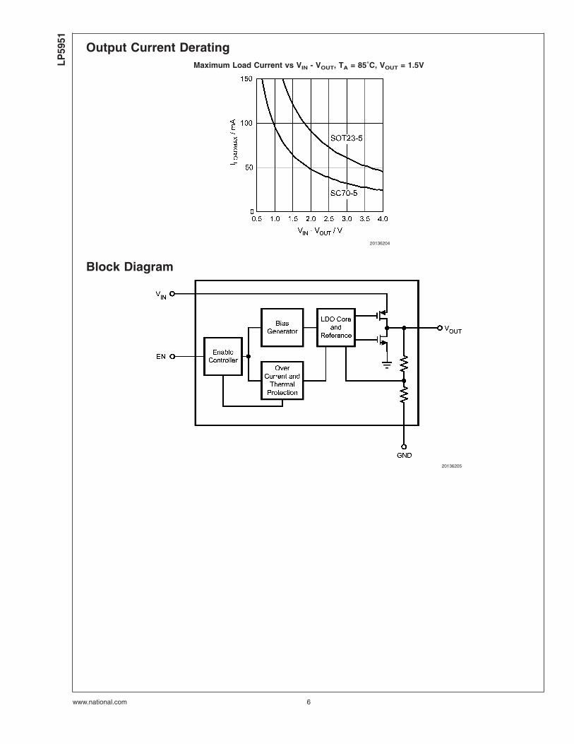
Output Current DeratingMaximum Load Current vs VIN - VOUT, TA = 85˚C, VOUT = 1.5V
20136204
Block Diagram
20136205
LP59
51
www.national.com 6
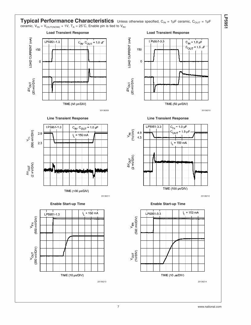
Typical Performance Characteristics Unless otherwise specified, CIN = 1µF ceramic, COUT = 1µFceramic, VIN = VOUT(NOM) + 1V, TA = 25˚C, Enable pin is tied to VIN.
Load Transient Response Load Transient Response
20136209 20136210
Line Transient Response Line Transient Response
20136211 20136212
Enable Start-up Time Enable Start-up Time
20136213 20136214
LP5951
www.national.com7
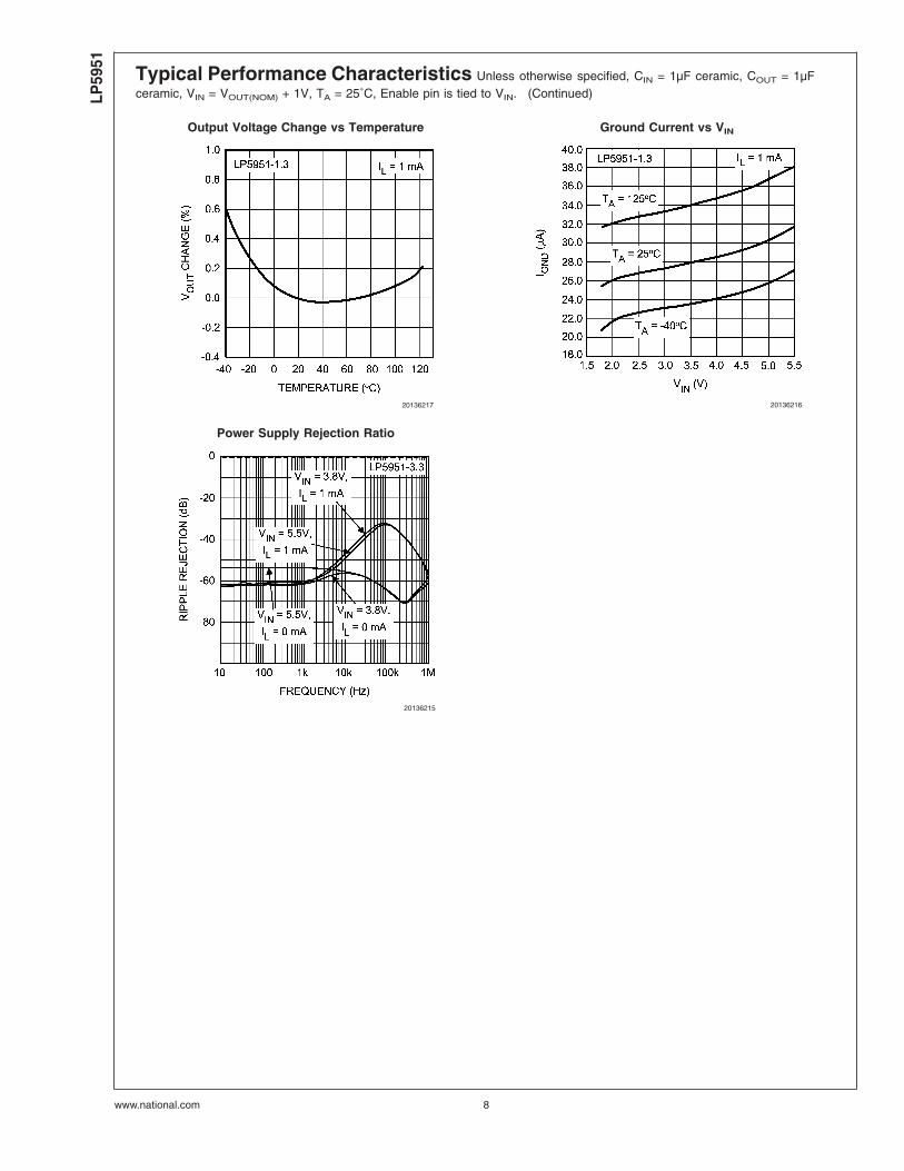
Typical Performance Characteristics Unless otherwise specified, CIN = 1µF ceramic, COUT = 1µFceramic, VIN = VOUT(NOM) + 1V, TA = 25˚C, Enable pin is tied to VIN. (Continued)
Output Voltage Change vs Temperature Ground Current vs VIN
20136217 20136216
Power Supply Rejection Ratio
20136215
LP59
51
www.national.com 8
Application Hints
POWER DISSIPATION AND DEVICE OPERATION
The permissible power dissipation for any package is ameasure of the capability of the device to pass heat from thepower source, the junctions of the IC, to the ultimate heatsink, the ambient environment. Thus the power dissipation isdependent on the ambient temperature and the thermalresistance across the various interfaces between the die andambient air.
As stated in (Note 5) in the electrical specification section,the allowable power dissipation for the device in a givenpackage can be calculated using the equation:
PD = (TJ(MAX) - TA) / θJA
With a θJA = 220˚C/W, the device in the SOT23-5 packagereturns a value of 454 mW with a maximum junction tem-perature of 125˚C at TA of 25˚C.
The actual power dissipation across the device can be esti-mated by the following equation:
PD ≈ (VIN - VOUT) * IOUT
This establishes the relationship between the power dissipa-tion allowed due to thermal consideration, the voltage dropacross the device, and the continuous current capability ofthe device. These two equations should be used to deter-mine the optimum operating conditions for the device in theapplication.
EXTERNAL CAPACITORS
As is common with most regulators, the LP5951 requiresexternal capacitors to ensure stable operation. The LP5951is specifically designed for portable applications requiringminimum board space and the smallest size components.These capacitors must be correctly selected for good perfor-mance.
INPUT CAPACITOR
An input capacitor is required for stability. It is recommendedthat a 1.0µF capacitor be connected between the LP5951input pin and ground (this capacitance value may be in-creased without limit).
This capacitor must be located a distance of not more than 1cm from the input pin and returned to a clean analogueground. Any good quality ceramic, tantalum, or film capacitormay be used at the input.
Important: Tantalum capacitors can suffer catastrophic fail-ures due to surge current when connected to a low-impedance source of power (like a battery or a very largecapacitor). If a tantalum capacitor is used at the input, it mustbe guaranteed by the manufacturer to have a surge currentrating sufficient for the application.
There are no requirements for the ESR (Equivalent SeriesResistance) on the input capacitor, but tolerance and tem-perature coefficient must be considered when selecting thecapacitor to ensure the capacitance will remain ≥0.7µF overthe entire operating temperature range.
OUTPUT CAPACITOR
The LP5951 is designed specifically to work with very smallceramic output capacitors. The following ceramic capacitors(dielectric types X7R, Z5U, or Y5V) are suitable as COUT inthe LP5951 application circuit:
• VOUT < 2.8V: 1.0µF
• VOUT ≥ 2.8V: 1.5µF
COUT can be increased up to 47µF, the ESR should bebetween 3 mΩ to 500 mΩ.
This capacitor must be located a distance of not more than1cm from the VOUT pin and returned to a clean analogueground.
It is also possible to use tantalum or film capacitors at thedevice output, VOUT, but these are not as attractive forreasons of size and cost (see the section Capacitor Charac-teristics).
CAPACITOR CHARACTERISTICS
The LP5951 is designed to work with ceramic capacitors onthe output to take advantage of the benefits they offer. Forcapacitance values in the range of 1µF to 4.7µF, ceramiccapacitors are the smallest, least expensive and have thelowest ESR values, thus making them best for eliminatinghigh frequency noise. The ESR of a typical 1µF ceramiccapacitor is in the range of 3mΩ to 40mΩ, which easilymeets the ESR requirement for stability for the LP5951.
For both input and output capacitors, careful interpretation ofthe capacitor specification is required to ensure correct de-vice operation. The capacitor value can change greatly, de-pending on the operating conditions and capacitor type.
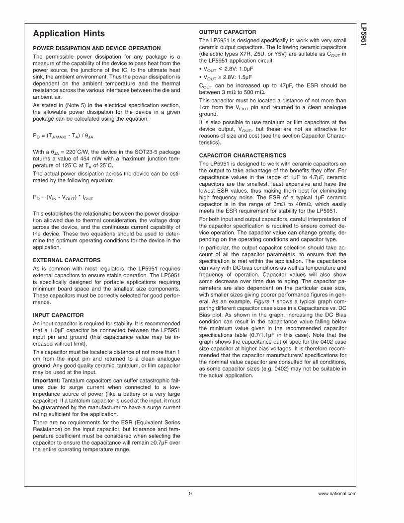
In particular, the output capacitor selection should take ac-count of all the capacitor parameters, to ensure that thespecification is met within the application. The capacitancecan vary with DC bias conditions as well as temperature andfrequency of operation. Capacitor values will also showsome decrease over time due to aging. The capacitor pa-rameters are also dependant on the particular case size,with smaller sizes giving poorer performance figures in gen-eral. As an example, Figure 1 shows a typical graph com-paring different capacitor case sizes in a Capacitance vs. DCBias plot. As shown in the graph, increasing the DC Biascondition can result in the capacitance value falling belowthe minimum value given in the recommended capacitorspecifications table (0.7/1.1µF in this case). Note that thegraph shows the capacitance out of spec for the 0402 casesize capacitor at higher bias voltages. It is therefore recom-mended that the capacitor manufacturers’ specifications forthe nominal value capacitor are consulted for all conditions,as some capacitor sizes (e.g. 0402) may not be suitable inthe actual application.
LP5951
www.national.com9
Application Hints (Continued)
The ceramic capacitor’s capacitance can vary with tempera-ture. The capacitor type X7R, which operates over a tem-perature range of -55˚C to +125˚C, will only vary the capaci-tance to within ±15%. The capacitor type X5R has a similartolerance over a reduced temperature range of -55˚C to+85˚C. Many large value ceramic capacitors, larger than 1µFare manufactured with Z5U or Y5V temperature characteris-tics. Their capacitance can drop by more than 50% as thetemperature varies from 25˚C to 85˚C. Therefore X7R isrecommended over Z5U and Y5V in applications where theambient temperature will change significantly above or be-low 25˚C.
Tantalum capacitors are less desirable than ceramic for useas output capacitors because they are more expensive whencomparing equivalent capacitance and voltage ratings in the1µF to 4.7µF range.
Another important consideration is that tantalum capacitorshave higher ESR values than equivalent size ceramics. Thismeans that while it may be possible to find a tantalumcapacitor with an ESR value within the stable range, it wouldhave to be larger in capacitance (which means bigger andmore costly) than a ceramic capacitor with the same ESRvalue. It should also be noted that the ESR of a typicaltantalum will increase about 2:1 as the temperature goesfrom 25˚C down to -40˚C, so some guard band must beallowed.
NO-LOAD STABILITY
The LP5951 will remain stable and in regulation with noexternal load. This is an important consideration in somecircuits, for example CMOS RAM keep-alive applications.
ENABLE OPERATION
The LP5951 may be switched ON or OFF by a logic input atthe Enable pin, VEN. A logic high at this pin will turn thedevice on. When the enable pin is low, the regulator output isoff and the device typically consumes 5nA.
If the application does not require the Enable switchingfeature, the VEN pin should be tied to VIN to keep theregulator output permanently on.
To ensure proper operation, the signal source used to drivethe VEN input must be able to swing above and below thespecified turn-on/off voltage thresholds listed in the ElectricalCharacteristics section under Enable Control Characteris-tics, VIL and VIH.
FAST TURN OFF AND ON
The controlled switch-off feature of the device provides a fastturn off by discharging the output capacitor via an internalFET device. This discharge is current limited by the RDSonof this switch.
Fast turn-on is guaranteed by an optimized architectureallowing a very fast ramp of the output voltage to reach thetarget voltage.
SHORT-CIRCUIT PROTECTION
The LP5951 is short circuit protected and in the event of apeak over-current condition, the output current through thePMOS will be limited.
If the over-current condition exists for a longer time, theaverage power dissipation will increase depending on theinput to output voltage difference until the thermal shutdowncircuitry will turn off the PMOS.
Please refer to the section on thermal information for powerdissipation calculations.
THERMAL-OVERLOAD PROTECTION
Thermal-Overload Protection limits the total power dissipa-tion in the LP5951. When the junction temperature exceedsTJ = 160˚C typ., the shutdown logic is triggered and thePMOS is turned off, allowing the device to cool down. Afterthe junction temperature dropped by 20˚C (temperature hys-teresis), the PMOS is activated again. This results in apulsed output voltage during continuous thermal-overloadconditions.
The Thermal-Overload Protection is designed to protect theLP5951 in the event of a fault condition. For normal, continu-ous operation, do not exceed the absolute maximum junc-tion temperature rating of TJ = +150˚C (see Absolute Maxi-mum Ratings).
REVERSE CURRENT PATH
The internal PFET pass device in LP5951 has an inherentparasitic body diode. During normal operation, the inputvoltage is higher than the output voltage and the parasiticdiode is reverse biased. However, if the output is pulledabove the input in an application, then current flows from theoutput to the input as the parasitic diode gets forward biased.The output can be pulled above the input as long as thecurrent in the parasitic diode is limited to 50mA.
For currents above this limit an external Schottky diode mustbe connected from VOUT to VIN (cathode on VIN, anode onVOUT).
20136206
FIGURE 1. Graph Showing A Typical Variation InCapacitance vs DC Bias
LP59
51
www.national.com 10
Application Hints (Continued)
Table 1: Suggested Capacitors and Their Suppliers
Capacitance / µF Model Vendor Type Case Size / Inch (mm)
1.0 C1608X5R1A105K TDK Ceramic, X5R 0603 (1608)
1.0 C1005X5R1A105K TDK Ceramic, X5R 0402 (1005)
1.5 C1608X5R1C155K TDK Ceramic, X5R 0603 (1608)
LP5951
www.national.com11
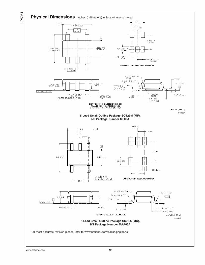
Physical Dimensions inches (millimeters) unless otherwise noted
20136207
5-Lead Small Outline Package SOT23-5 (MF),NS Package Number MF05A
20136218
5-Lead Small Outline Package SC70-5 (MG),NS Package Number MAA05A
For most accurate revision please refer to www.national.com/packaging/parts/
LP59
51
www.national.com 12
Notes
National does not assume any responsibility for use of any circuitry described, no circuit patent licenses are implied and National reservesthe right at any time without notice to change said circuitry and specifications.
For the most current product information visit us at www.national.com.
LIFE SUPPORT POLICY
NATIONAL’S PRODUCTS ARE NOT AUTHORIZED FOR USE AS CRITICAL COMPONENTS IN LIFE SUPPORT DEVICES OR SYSTEMSWITHOUT THE EXPRESS WRITTEN APPROVAL OF THE PRESIDENT AND GENERAL COUNSEL OF NATIONAL SEMICONDUCTORCORPORATION. As used herein:
1. Life support devices or systems are devices or systemswhich, (a) are intended for surgical implant into the body, or(b) support or sustain life, and whose failure to perform whenproperly used in accordance with instructions for useprovided in the labeling, can be reasonably expected to resultin a significant injury to the user.
2. A critical component is any component of a life support deviceor system whose failure to perform can be reasonablyexpected to cause the failure of the life support device orsystem, or to affect its safety or effectiveness.
BANNED SUBSTANCE COMPLIANCE
National Semiconductor follows the provisions of the Product Stewardship Guide for Customers (CSP-9-111C2) and Banned Substancesand Materials of Interest Specification (CSP-9-111S2) for regulatory environmental compliance. Details may be found at:www.national.com/quality/green.
Lead free products are RoHS compliant.
National SemiconductorAmericas CustomerSupport CenterEmail: [email protected]: 1-800-272-9959
National SemiconductorEurope Customer Support Center
Fax: +49 (0) 180-530 85 86Email: [email protected]
Deutsch Tel: +49 (0) 69 9508 6208English Tel: +44 (0) 870 24 0 2171Français Tel: +33 (0) 1 41 91 8790
National SemiconductorAsia Pacific CustomerSupport CenterEmail: [email protected]
National SemiconductorJapan Customer Support CenterFax: 81-3-5639-7507Email: [email protected]: 81-3-5639-7560
www.national.com
LP5951
Micropow
er,150mA
Low-D
ropoutC
MO
SVoltage
Regulator