lt6656 (rev. d) - analog devices
TRANSCRIPT
LT6656
1Rev D
For more information www.analog.comDocument Feedback
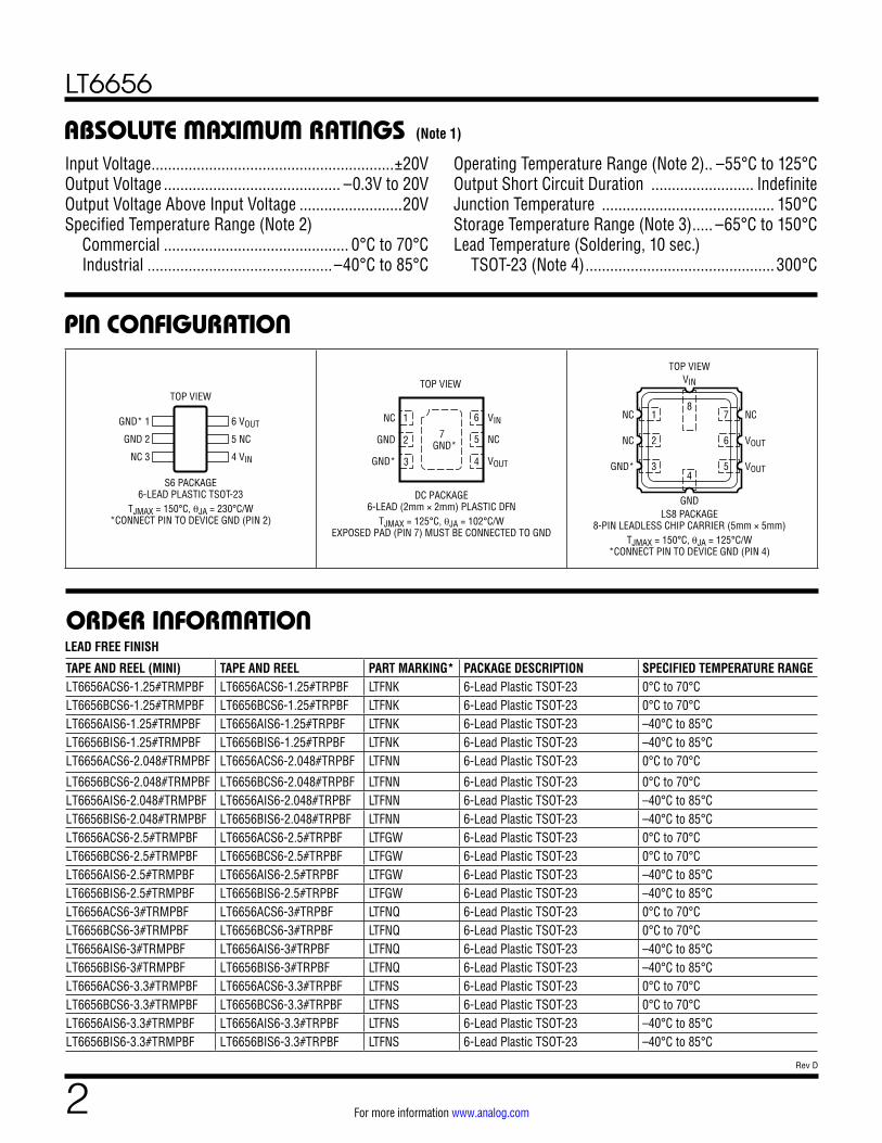
TYPICAL APPLICATION Output Voltage Temperature Drift
TEMPERATURE (°C)–40
2.498
2.499
V OUT
(V)
2.500
2.501
2.502
2.503
–20 0 20 406652 TA01b
60 80
38 TYPICAL UNITSLT6656-2.5
Basic Connection
DESCRIPTION
1µA Precision Series Voltage Reference
The LT®6656 is a tiny precision voltage reference that draws less than 1µA of supply current and can operate with a supply voltage within 10mV of the output voltage. The LT6656 offers an initial accuracy of 0.05% and tem-perature drift of 10ppm/°C. The combined low power and precision characteristics are ideal for portable and battery powered instrumentation.
The LT6656 can supply up to 5mA of output drive with 65ppm/mA of load regulation, allowing it to be used as the supply voltage and the reference input to a low power ADC. The LT6656 can accept a supply voltage up to 18V and withstand the reversal of the input connections.
The LT6656 output is stable with 1µF or larger output capacitance and operates with a wide range of output capacitor ESR.
This reference is fully specified for operation from –40°C to 85°C, and is functional over the extreme temperature range of –55°C to 125°C. Low hysteresis and a consistent temperature drift are obtained through advanced design, processing and packaging techniques.
The LT6656 is offered in the 6-lead SOT-23, (2mm × 2mm) DFN, and 8-lead LS8 Packages. The LS8 is a 5mm × 5mm surface mount hermetic package that provides outstanding stability.
FEATURES
APPLICATIONS
n Ultralow Supply Current: 850nAn Low Drift
A Grade: 10 ppm/°C Max B Grade: 20 ppm/°C Max
n High Accuracy A Grade: 0.05% Max B Grade: 0.1% Max
n Long-Term Drift: 15ppm/√kHr (LS8 Package)n No Humidity Sensitivity (LS8 Package)n High Output Drive Current: 5mA Minn Low Dropout Voltage: 10mV Maxn Fully Specified from –40°C to 85°Cn Operational from –55°C to 125°Cn Wide Supply Range to 18Vn Reverse Input/Output Protectionn Available Output Voltage Options:
1.25V, 2.048V, 2.5V, 2.8V, 3V, 3.3V, 4.096V and 5Vn Available in Low Profile (1mm) ThinSOT™,
(2mm × 2mm) DFN and High Stability Hermetic (5mm × 5mm) LS8 Packages
n Precision A/D and D/A Convertersn Portable Gas Monitorsn Battery- or Solar-Powered Systemsn Precision Regulatorsn Low Voltage Signal Processingn Micropower Remote Sensing
2.51V ≤ VIN ≤ 18V
0.1µF 1µF
VOUT2.5V
6656 TA01a
LT6656-2.5VIN VOUT
GND
All registered trademarks and trademarks are the property of their respective owners.
LT6656
2Rev D
For more information www.analog.com
ABSOLUTE MAXIMUM RATINGSInput Voltage ...........................................................±20VOutput Voltage ........................................... –0.3V to 20VOutput Voltage Above Input Voltage .........................20VSpecified Temperature Range (Note 2)
Commercial ............................................. 0°C to 70°C Industrial .............................................–40°C to 85°C
(Note 1)
ORDER INFORMATION
TAPE AND REEL (MINI) TAPE AND REEL PART MARKING* PACKAGE DESCRIPTION SPECIFIED TEMPERATURE RANGELT6656ACS6-1.25#TRMPBF LT6656ACS6-1.25#TRPBF LTFNK 6-Lead Plastic TSOT-23 0°C to 70°CLT6656BCS6-1.25#TRMPBF LT6656BCS6-1.25#TRPBF LTFNK 6-Lead Plastic TSOT-23 0°C to 70°CLT6656AIS6-1.25#TRMPBF LT6656AIS6-1.25#TRPBF LTFNK 6-Lead Plastic TSOT-23 –40°C to 85°CLT6656BIS6-1.25#TRMPBF LT6656BIS6-1.25#TRPBF LTFNK 6-Lead Plastic TSOT-23 –40°C to 85°CLT6656ACS6-2.048#TRMPBF LT6656ACS6-2.048#TRPBF LTFNN 6-Lead Plastic TSOT-23 0°C to 70°C
LT6656BCS6-2.048#TRMPBF LT6656BCS6-2.048#TRPBF LTFNN 6-Lead Plastic TSOT-23 0°C to 70°CLT6656AIS6-2.048#TRMPBF LT6656AIS6-2.048#TRPBF LTFNN 6-Lead Plastic TSOT-23 –40°C to 85°CLT6656BIS6-2.048#TRMPBF LT6656BIS6-2.048#TRPBF LTFNN 6-Lead Plastic TSOT-23 –40°C to 85°CLT6656ACS6-2.5#TRMPBF LT6656ACS6-2.5#TRPBF LTFGW 6-Lead Plastic TSOT-23 0°C to 70°CLT6656BCS6-2.5#TRMPBF LT6656BCS6-2.5#TRPBF LTFGW 6-Lead Plastic TSOT-23 0°C to 70°CLT6656AIS6-2.5#TRMPBF LT6656AIS6-2.5#TRPBF LTFGW 6-Lead Plastic TSOT-23 –40°C to 85°CLT6656BIS6-2.5#TRMPBF LT6656BIS6-2.5#TRPBF LTFGW 6-Lead Plastic TSOT-23 –40°C to 85°CLT6656ACS6-3#TRMPBF LT6656ACS6-3#TRPBF LTFNQ 6-Lead Plastic TSOT-23 0°C to 70°CLT6656BCS6-3#TRMPBF LT6656BCS6-3#TRPBF LTFNQ 6-Lead Plastic TSOT-23 0°C to 70°CLT6656AIS6-3#TRMPBF LT6656AIS6-3#TRPBF LTFNQ 6-Lead Plastic TSOT-23 –40°C to 85°CLT6656BIS6-3#TRMPBF LT6656BIS6-3#TRPBF LTFNQ 6-Lead Plastic TSOT-23 –40°C to 85°CLT6656ACS6-3.3#TRMPBF LT6656ACS6-3.3#TRPBF LTFNS 6-Lead Plastic TSOT-23 0°C to 70°CLT6656BCS6-3.3#TRMPBF LT6656BCS6-3.3#TRPBF LTFNS 6-Lead Plastic TSOT-23 0°C to 70°CLT6656AIS6-3.3#TRMPBF LT6656AIS6-3.3#TRPBF LTFNS 6-Lead Plastic TSOT-23 –40°C to 85°CLT6656BIS6-3.3#TRMPBF LT6656BIS6-3.3#TRPBF LTFNS 6-Lead Plastic TSOT-23 –40°C to 85°C
Operating Temperature Range (Note 2).. –55°C to 125°COutput Short Circuit Duration ......................... IndefiniteJunction Temperature .......................................... 150°CStorage Temperature Range (Note 3) ..... –65°C to 150°CLead Temperature (Soldering, 10 sec.) TSOT-23 (Note 4) .............................................. 300°C
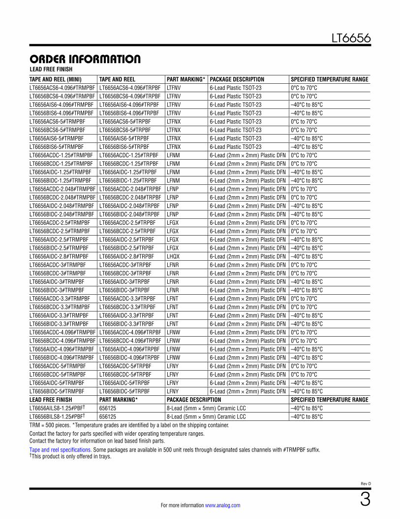
GND* 1
GND 2
NC 3
6 VOUT
5 NC
4 VIN
TOP VIEW
S6 PACKAGE6-LEAD PLASTIC TSOT-23
TJMAX = 150°C, θJA = 230°C/W*CONNECT PIN TO DEVICE GND (PIN 2)
TOP VIEW
VIN
NC
VOUT
NC
GND
GND*
DC PACKAGE6-LEAD (2mm × 2mm) PLASTIC DFN
TJMAX = 125°C, θJA = 102°C/WEXPOSED PAD (PIN 7) MUST BE CONNECTED TO GND
4
57 GND*
6
3
2
1 1
2
3
NC
NC
GND*
7
6
5
NC
VOUT
VOUT4
GND
8
VIN
TOP VIEW
LS8 PACKAGE8-PIN LEADLESS CHIP CARRIER (5mm × 5mm)
TJMAX = 150°C, θJA = 125°C/W*CONNECT PIN TO DEVICE GND (PIN 4)
PIN CONFIGURATION
LEAD FREE FINISH
LT6656
3Rev D
For more information www.analog.com
ORDER INFORMATIONLEAD FREE FINISH
TAPE AND REEL (MINI) TAPE AND REEL PART MARKING* PACKAGE DESCRIPTION SPECIFIED TEMPERATURE RANGELT6656ACS6-4.096#TRMPBF LT6656ACS6-4.096#TRPBF LTFNV 6-Lead Plastic TSOT-23 0°C to 70°CLT6656BCS6-4.096#TRMPBF LT6656BCS6-4.096#TRPBF LTFNV 6-Lead Plastic TSOT-23 0°C to 70°CLT6656AIS6-4.096#TRMPBF LT6656AIS6-4.096#TRPBF LTFNV 6-Lead Plastic TSOT-23 –40°C to 85°CLT6656BIS6-4.096#TRMPBF LT6656BIS6-4.096#TRPBF LTFNV 6-Lead Plastic TSOT-23 –40°C to 85°CLT6656ACS6-5#TRMPBF LT6656ACS6-5#TRPBF LTFNX 6-Lead Plastic TSOT-23 0°C to 70°CLT6656BCS6-5#TRMPBF LT6656BCS6-5#TRPBF LTFNX 6-Lead Plastic TSOT-23 0°C to 70°CLT6656AIS6-5#TRMPBF LT6656AIS6-5#TRPBF LTFNX 6-Lead Plastic TSOT-23 –40°C to 85°CLT6656BIS6-5#TRMPBF LT6656BIS6-5#TRPBF LTFNX 6-Lead Plastic TSOT-23 –40°C to 85°CLT6656ACDC-1.25#TRMPBF LT6656ACDC-1.25#TRPBF LFNM 6-Lead (2mm × 2mm) Plastic DFN 0°C to 70°CLT6656BCDC-1.25#TRMPBF LT6656BCDC-1.25#TRPBF LFNM 6-Lead (2mm × 2mm) Plastic DFN 0°C to 70°CLT6656AIDC-1.25#TRMPBF LT6656AIDC-1.25#TRPBF LFNM 6-Lead (2mm × 2mm) Plastic DFN –40°C to 85°CLT6656BIDC-1.25#TRMPBF LT6656BIDC-1.25#TRPBF LFNM 6-Lead (2mm × 2mm) Plastic DFN –40°C to 85°CLT6656ACDC-2.048#TRMPBF LT6656ACDC-2.048#TRPBF LFNP 6-Lead (2mm × 2mm) Plastic DFN 0°C to 70°CLT6656BCDC-2.048#TRMPBF LT6656BCDC-2.048#TRPBF LFNP 6-Lead (2mm × 2mm) Plastic DFN 0°C to 70°CLT6656AIDC-2.048#TRMPBF LT6656AIDC-2.048#TRPBF LFNP 6-Lead (2mm × 2mm) Plastic DFN –40°C to 85°CLT6656BIDC-2.048#TRMPBF LT6656BIDC-2.048#TRPBF LFNP 6-Lead (2mm × 2mm) Plastic DFN –40°C to 85°CLT6656ACDC-2.5#TRMPBF LT6656ACDC-2.5#TRPBF LFGX 6-Lead (2mm × 2mm) Plastic DFN 0°C to 70°CLT6656BCDC-2.5#TRMPBF LT6656BCDC-2.5#TRPBF LFGX 6-Lead (2mm × 2mm) Plastic DFN 0°C to 70°CLT6656AIDC-2.5#TRMPBF LT6656AIDC-2.5#TRPBF LFGX 6-Lead (2mm × 2mm) Plastic DFN –40°C to 85°CLT6656BIDC-2.5#TRMPBF LT6656BIDC-2.5#TRPBF LFGX 6-Lead (2mm × 2mm) Plastic DFN –40°C to 85°CLT6656AIDC-2.8#TRMPBF LT6656AIDC-2.8#TRPBF LHQX 6-Lead (2mm × 2mm) Plastic DFN –40°C to 85°CLT6656ACDC-3#TRMPBF LT6656ACDC-3#TRPBF LFNR 6-Lead (2mm × 2mm) Plastic DFN 0°C to 70°CLT6656BCDC-3#TRMPBF LT6656BCDC-3#TRPBF LFNR 6-Lead (2mm × 2mm) Plastic DFN 0°C to 70°CLT6656AIDC-3#TRMPBF LT6656AIDC-3#TRPBF LFNR 6-Lead (2mm × 2mm) Plastic DFN –40°C to 85°CLT6656BIDC-3#TRMPBF LT6656BIDC-3#TRPBF LFNR 6-Lead (2mm × 2mm) Plastic DFN –40°C to 85°CLT6656ACDC-3.3#TRMPBF LT6656ACDC-3.3#TRPBF LFNT 6-Lead (2mm × 2mm) Plastic DFN 0°C to 70°CLT6656BCDC-3.3#TRMPBF LT6656BCDC-3.3#TRPBF LFNT 6-Lead (2mm × 2mm) Plastic DFN 0°C to 70°CLT6656AIDC-3.3#TRMPBF LT6656AIDC-3.3#TRPBF LFNT 6-Lead (2mm × 2mm) Plastic DFN –40°C to 85°CLT6656BIDC-3.3#TRMPBF LT6656BIDC-3.3#TRPBF LFNT 6-Lead (2mm × 2mm) Plastic DFN –40°C to 85°CLT6656ACDC-4.096#TRMPBF LT6656ACDC-4.096#TRPBF LFNW 6-Lead (2mm × 2mm) Plastic DFN 0°C to 70°CLT6656BCDC-4.096#TRMPBF LT6656BCDC-4.096#TRPBF LFNW 6-Lead (2mm × 2mm) Plastic DFN 0°C to 70°CLT6656AIDC-4.096#TRMPBF LT6656AIDC-4.096#TRPBF LFNW 6-Lead (2mm × 2mm) Plastic DFN –40°C to 85°CLT6656BIDC-4.096#TRMPBF LT6656BIDC-4.096#TRPBF LFNW 6-Lead (2mm × 2mm) Plastic DFN –40°C to 85°CLT6656ACDC-5#TRMPBF LT6656ACDC-5#TRPBF LFNY 6-Lead (2mm × 2mm) Plastic DFN 0°C to 70°CLT6656BCDC-5#TRMPBF LT6656BCDC-5#TRPBF LFNY 6-Lead (2mm × 2mm) Plastic DFN 0°C to 70°CLT6656AIDC-5#TRMPBF LT6656AIDC-5#TRPBF LFNY 6-Lead (2mm × 2mm) Plastic DFN –40°C to 85°CLT6656BIDC-5#TRMPBF LT6656BIDC-5#TRPBF LFNY 6-Lead (2mm × 2mm) Plastic DFN –40°C to 85°CLEAD FREE FINISH PART MARKING* PACKAGE DESCRIPTION SPECIFIED TEMPERATURE RANGELT6656AILS8-1.25#PBF† 656125 8-Lead (5mm × 5mm) Ceramic LCC –40°C to 85°CLT6656BILS8-1.25#PBF† 656125 8-Lead (5mm × 5mm) Ceramic LCC –40°C to 85°CTRM = 500 pieces. *Temperature grades are identified by a label on the shipping container.Contact the factory for parts specified with wider operating temperature ranges. Contact the factory for information on lead based finish parts.Tape and reel specifications. Some packages are available in 500 unit reels through designated sales channels with #TRMPBF suffix. †This product is only offered in trays.

LT6656
4Rev D
For more information www.analog.com
AVAILABLE OPTIONS
OUTPUT VOLTAGE INITIAL ACCURACYTEMPERATURE COEFFICIENT
SPECIFIED TEMPERATURE RANGE
0°C TO 70°C –40°C TO 85°C
ORDER PART NUMBER* ORDER PART NUMBER*
1.250V 0.05% 10ppm/°C LT6656ACS6-1.25 LT6656AIS6-1.25
0.05% 10ppm/°C N/A LT6656AILS8-1.25
0.10% 20ppm/°C LT6656BCS6-1.25 LT6656BIS6-1.25
0.10% 10ppm/°C LT6656ACDC-1.25 LT6656AIDC-1.25
0.10% 15ppm/°C N/A LT6656BILS8-1.25
0.20% 20ppm/°C LT6656BCDC-1.25 LT6656BIDC-1.25
2.048V 0.05% 10ppm/°C LT6656ACS6-2.048 LT6656AIS6-2.048
0.10% 20ppm/°C LT6656BCS6-2.048 LT6656BIS6-2.048
0.10% 10ppm/°C LT6656ACDC-2.048 LT6656AIDC-2.048
0.20% 20ppm/°C LT6656BCDC-2.048 LT6656BIDC-2.048
2.500V 0.05% 10ppm/°C LT6656ACS6-2.5 LT6656AIS6-2.5
0.10% 20ppm/°C LT6656BCS6-2.5 LT6656BIS6-2.5
0.10% 10ppm/°C LT6656ACDC-2.5 LT6656AIDC-2.5
0.20% 20ppm/°C LT6656BCDC-2.5 LT6656BIDC-2.5
2.800V 0.10% 10ppm/°C N/A LT6656AIDC-2.8
3.000V 0.05% 10ppm/°C LT6656ACS6-3 LT6656AIS6-3
0.10% 20ppm/°C LT6656BCS6-3 LT6656BIS6-3
0.10% 10ppm/°C LT6656ACDC-3 LT6656AIDC-3
0.20% 20ppm/°C LT6656BCDC-3 LT6656BIDC-3
3.300V 0.05% 10ppm/°C LT6656ACS6-3.3 LT6656AIS6-3.3
0.10% 20ppm/°C LT6656BCS6-3.3 LT6656BIS6-3.3
0.10% 10ppm/°C LT6656ACDC-3.3 LT6656AIDC-3.3
0.20% 20ppm/°C LT6656BCDC-3.3 LT6656BIDC-3.3
4.096V 0.05% 10ppm/°C LT6656ACS6-4.096 LT6656AIS6-4.096
0.10% 20ppm/°C LT6656BCS6-4.096 LT6656BIS6-4.096
0.10% 10ppm/°C LT6656ACDC-4.096 LT6656AIDC-4.096
0.20% 20ppm/°C LT6656BCDC-4.096 LT6656BIDC-4.096
5.000V 0.05% 10ppm/°C LT6656ACS6-5 LT6656AIS6-5
0.10% 20ppm/°C LT6656BCS6-5 LT6656BIS6-5
0.10% 10ppm/°C LT6656ACDC-5 LT6656AIDC-5
0.20% 20ppm/°C LT6656BCDC-5 LT6656BIDC-5
*See Order Information section for complete part number listing.
LT6656
5Rev D
For more information www.analog.com
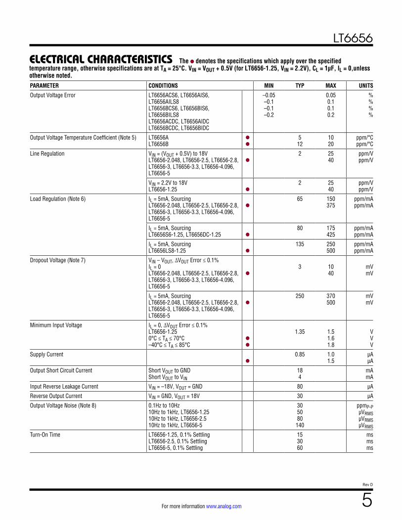
ELECTRICAL CHARACTERISTICS The l denotes the specifications which apply over the specified temperature range, otherwise specifications are at TA = 25°C. VIN = VOUT + 0.5V (for LT6656-1.25, VIN = 2.2V), CL = 1μF, IL = 0,unless otherwise noted.PARAMETER CONDITIONS MIN TYP MAX UNITS
Output Voltage Error LT6656ACS6, LT6656AIS6, LT6656AILS8 LT6656BCS6, LT6656BIS6, LT6656BILS8 LT6656ACDC, LT6656AIDC LT6656BCDC, LT6656BIDC
–0.05 –0.1 –0.1 –0.2
0.05 0.1 0.1 0.2
% % % %
Output Voltage Temperature Coefficient (Note 5) LT6656A LT6656B
l
l
5 12
10 20
ppm/°C ppm/°C
Line Regulation VIN = (VOUT + 0.5V) to 18V LT6656-2.048, LT6656-2.5, LT6656-2.8, LT6656-3, LT6656-3.3, LT6656-4.096, LT6656-5
l
2 25 40
ppm/V ppm/V
VIN = 2.2V to 18V LT6656-1.25
l
2 25 40
ppm/V ppm/V
Load Regulation (Note 6) IL = 5mA, Sourcing LT6656-2.048, LT6656-2.5, LT6656-2.8, LT6656-3, LT6656-3.3, LT6656-4.096, LT6656-5
l
65 150 375
ppm/mA ppm/mA
IL = 5mA, Sourcing LT6656S6-1.25, LT6656DC-1.25
l
80 175 425
ppm/mA ppm/mA
IL = 5mA, Sourcing LT6656LS8-1.25
l
135 250 500
ppm/mA ppm/mA
Dropout Voltage (Note 7) VIN – VOUT, ∆VOUT Error ≤ 0.1% IL = 0 LT6656-2.048, LT6656-2.5, LT6656-2.8, LT6656-3, LT6656-3.3, LT6656-4.096, LT6656-5
l
3
10 40
mV mV
IL = 5mA, Sourcing LT6656-2.048, LT6656-2.5, LT6656-2.8, LT6656-3, LT6656-3.3, LT6656-4.096, LT6656-5
l
250 370 500
mV mV
Minimum Input Voltage IL = 0, ∆VOUT Error ≤ 0.1% LT6656-1.25 0°C ≤ TA ≤ 70°C –40°C ≤ TA ≤ 85°C
l
l
1.35
1.5 1.6 1.8
V V V
Supply Current
l
0.85 1.0 1.5
µA µA
Output Short Circuit Current Short VOUT to GND Short VOUT to VIN
18 4
mA mA
Input Reverse Leakage Current VIN = –18V, VOUT = GND 80 µA
Reverse Output Current VIN = GND, VOUT = 18V 30 µA
Output Voltage Noise (Note 8) 0.1Hz to 10Hz 10Hz to 1kHz, LT6656-1.25 10Hz to 1kHz, LT6656-2.5 10Hz to 1kHz, LT6656-5
30 50 80
140
ppmP-P µVRMS µVRMS µVRMS
Turn-On Time LT6656-1.25, 0.1% Settling LT6656-2.5, 0.1% Settling LT6656-5, 0.1% Settling
15 30 60
ms ms ms

LT6656
6Rev D
For more information www.analog.com
ELECTRICAL CHARACTERISTICS
Note 1: Stresses beyond those listed under Absolute Maximum Ratings may cause permanent damage to the device. Exposure to any Absolute Maximum Rating condition for extended periods may affect device reliability and lifetime.Note 2: The LT6656C is guaranteed to meet specified performance from 0°C to 70°C. The LT6656C is designed, characterized and expected to meet specified performance from –40°C to 85°C but is not tested or QA sampled at these temperatures. The LT6656I is guaranteed to meet specified performance from –40°C to 85°C. By design, the LT6656 is guaranteed functional over the operating temperature range of –55°C to 125°C.Note 3: If the LT6656 is stored outside of the specified temperature range, the output may shift due to hysteresis.Note 4: The stated temperature is typical for soldering of the leads during manual rework. For detailed IR reflow recommendations, refer to the Applications section.Note 5: Temperature coefficient is measured by dividing the maximum change in output voltage by the specified temperature range.Note 6: Load regulation is measured with a pulse from no load to the specified load current. Output changes due to die temperature change must be taken into account separately.
Note 7: Excludes load regulation errors.Note 8: Peak-to-peak noise is measured with a 3-pole highpass filter at 0.1Hz and a 4-pole lowpass filter at 10Hz. The unit is enclosed in a still-air environment to eliminate thermocouple effects on the leads. The test time is 10 seconds. RMS noise is measured on a spectrum analyzer in a shielded environment.Note 9: Long term stability typically has a logarithmic characteristic and therefore, changes after 1000 hours tend to be much smaller than before that time. Total drift in the second thousand hours is normally less than one third that of the first thousand hours with a continuing trend toward reduced drift with time. Long-term stability will also be affected by differential stresses between the IC and the board material created during board assembly.Note 10: Hysteresis in output voltage is created by mechanical stress that differs depending on whether the IC was previously at a higher or lower temperature. Output voltage is always measured at 25°C, but the IC is cycled to the hot or cold temperature limit before successive measurements. For instruments that are stored at well controlled temperatures (within 20 or 30 degrees of operational temperature) hysteresis is usually not a dominant error source. Typical hysteresis is the worst-case of 25°C to cold to 25°C or 25°C to hot to 25°C, preconditioned by one thermal cycle.
TYPICAL PERFORMANCE CHARACTERISTICS
Output Voltage Temperature Drift Typical VOUT Distribution Supply Current vs Input Voltage100
10
1
0.1
INPUT VOLTAGE (V)0
SUPP
LY C
URRE
NT (µ
A)
10 186 14
6656 G17
208 164 122
TA = 125°CTA = 85°CTA = 25°CTA = –40°CTA = –55°C
1.25V OPTION
TEMPERATURE (°C)–60 –40
–1000
0
1000
2000
CHAN
GE IN
OUT
PUT
VOLT
AGE
(ppm
)
3000
5000
6000
7000
8000
9000
4000
10000
–20 0 20 40
6652 G01
60 12010080
ALL OPTIONS25 TYPICAL UNITSNORMALIZED AT 25°CCL = 1µFIL = 0
OUTPUT VOLTAGE ERROR (%)–0.10 0.10
NUM
BER
OF U
NITS
200
20
180
140
100
60
160
120
80
40
0
6656 G02
–0.02–0.06 0.060.020
ALL OPTIONSCL = 1µFIL = 0TA = 25°C
The l denotes the specifications which apply over the specified temperature range, otherwise specifications are at TA = 25°C. VIN = VOUT + 0.5V (for LT6656-1.25, VIN = 2.2V), CL = 1μF, IL = 0,unless otherwise noted.Long Term Drift of Output Voltage (Note 9) LT6656S6, LT6656DC
LT6656LS850 15
ppm/√kHr ppm/√kHr
Hysteresis (Note 10) LT6656S6, LT6656DC ∆T = 0°C to 70°C ∆T = –40°C to 85°C
25 70
ppm ppm
LT6656LS8 ∆T = 0°C to 70°C ∆T = –40°C to 85°C
15 55
ppm ppm

LT6656
7Rev D
For more information www.analog.com
TYPICAL PERFORMANCE CHARACTERISTICS
Power Supply Rejection Ratio vs Frequency
Dropout Voltage vs Load Current
Load Regulation (Sourcing) Load Regulation (Sinking)
Line Regulation
Supply Current vs Input Voltage100
10
1
0.1
INPUT VOLTAGE (V)0
SUPP
LY C
URRE
NT (µ
A)
10 186 14
6656 G03
208 164 122
TA = 125°CTA = 85°CTA = 25°CTA = –55°C
2.048V TO 5V OPTIONS
2.5V OPTION SHOWNVON MOVES WITH VOLTAGE OPTION
VON
0.1µ 1µ 1m 10m100µ10µ
1000
100
10
1
LOAD CURRENT (A)
DROP
OUT
VOLT
AGE
(mV)
6656 G04
TA = 125°CTA = 85°CTA = 25°CTA = –55°C
2.048V TO 5V OPTIONSVIN – VOUTINITIAL VIN = VOUT + 0.5V∆VOUT = 0.1%
750
500
250
0
–750
–500
–250
OUTP
UT V
OLTA
GE C
HANG
E (p
pm)
6656 G05
TA = 125°CTA = 85°CTA = 25°CTA = –55°C
2.048V TO 5V OPTIONSVIN = VOUT + 0.5VCL = 1µF
0.1µ 1µ 1m 10m100µ10µLOAD CURRENT (A)
10µ 1m100µ
5.0
2.0
1.5
3.0
2.5
4.0
3.5
4.5
1.0
0.5
0
–0.5
LOAD CURRENT (A)
OUTP
UT V
OLTA
GE C
HANG
E (%
)
6656 G06
TA = 85°C, 125°CTA = 25°CTA = –40°CTA = –55°C
ALL OPTIONSVIN = VOUT + 0.5VCL = 1µF
1000
900
800
700
600
500
400
300
200
100
0
–200
–100
INPUT VOLTAGE (V)0
OUTP
UT V
OLTA
GE C
HANG
E (p
pm)
10 186 14
6656 G08
208 164 122
TA = 125°CTA = 85°CTA = 25°CTA = –55°C
ALL OPTIONSIL = 0CL = 1µF
2.5V OPTION SHOWNVON MOVES WITH VOLTAGE OPTION
VON
FREQUENCY (Hz)
POW
ER S
UPPL
Y RE
JECT
ION
RATI
O (d
B)
6656 G09
90
80
70
60
50
40
30
10
20
010 1k 10k100
VIN = VOUT + 0.5VCL = 1µFIL = 0
1.25V OPTION2.5V OPTION5V OPTION
Minimum Supply Voltage vs Load Current
2.0
1.8
1.6
1.4
1.2
0.8
1.0MIN
IMUM
SUP
PLY
VOLT
AGE
(V)
6656 G18
1.25V OPTIONINITIAL VIN = 2.2V∆VOUT = 0.1%
TA = 125°CTA = 85°CTA = 25°CTA = –40°CTA = –55°C
0.1µ 1µ 1m 10m100µ10µLOAD CURRENT (A)
Load Regulation (Sourcing)500
250
0
–1000
–750
–500
–250
OUTP
UT V
OLTA
GE C
HANG
E (p
pm)
6656 G19
TA = 125°CTA = 85°CTA = 25°CTA = –40°CTA = –55°C
1.25V OPTIONVIN = 1.75VCL = 1µF
0.1µ 1µ 1m 10m100µ10µLOAD CURRENT (A)
Power Supply Rejection Ratio vs Frequency
FREQUENCY (Hz)
POW
ER S
UPPL
Y RE
JECT
ION
RATI
O (d
B)
6656 G20
90
80
70
60
50
40
30
10
20
–10
0
10 1k 10k100
2.5V OPTIONVIN = 3V
IL = 0, CL = 1µFIL = 0, CL = 10µFIL = 1mA, CL = 1µFIL = 1mA, CL = 10µF

LT6656
8Rev D
For more information www.analog.com
Output Impedance vs Frequency
FREQUENCY (Hz)
OUTP
UT IM
PEDA
NCE
(Ω)
6656 G21
10k
1k
100
10
110 1k 10k100
VIN = VOUT + 0.5VCL = 1µFIL = 0
1.25V OPTION2.5V OPTION5V OPTION
TYPICAL PERFORMANCE CHARACTERISTICS
Reverse Output CurrentReverse Input Current
0 15 20105
100
10
1
OUTPUT VOLTAGE (V)
REVE
RSE
OUTP
UT C
URRE
NT (µ
A)
6656 G12
TA = 125°CTA = 85°CTA = 25°CTA = –55°C
ALL OPTIONSVIN = GND
INPUT VOLTAGE (V)
REVE
RSE
INPU
T CU
RREN
T (µ
A)
6656 G11
1000
100
10
1
00 –2 –4 –6 –8 –20–18–16–14–12–10
TA = 125°CTA = 85°CTA = 25°CTA = –55°C
ALL OPTIONSVOUT = GND
Output Noise Voltage Spectrum vs Load Capacitance
FREQUENCY (Hz)
NOIS
E VO
LTAG
E (µ
V/√H
z)
6656 G15
40
35
30
25
20
15
10
5
01 100 1k10
2.5V OPTIONVIN = 3VIL = 0 CL = 47µF
CL = 4.7µF
CL = 0.47µF
Output Noise 0.1Hz to 10Hz
Output Voltage Noise Spectrum vs Load Current
OUTP
UT N
OISE
(20p
pm/D
IV)
TIME (1s/DIV)6656 G13
ALL OPTIONSVIN = VOUT + 0.5VCL = 1µFIL = 0
FREQUENCY (Hz)
NOIS
E VO
LTAG
E (µ
V/√H
z)
6656 G14
16
14
12
10
8
6
4
2
010 1k 10k100
2.5V OPTIONVIN = 3VCL = 1µF
IL = 0IL = 10µAIL = 250µAIL = 1mA
Ground Current vs Load Current
LOAD CURRENT (A)
GROU
ND C
URRE
NT (µ
A)
6656 G07
1000
100
10
110µ 1m 10m100µ
TA = 125°CTA = 85°CTA = 25°CTA = –55°C
ALL OPTIONSVIN = VOUT + 0.5VCL = 1µF
Output Impedance vs Frequency
FREQUENCY (Hz)
OUTP
UT IM
PEDA
NCE
(Ω)
6656 G22
10k
1k
100
10
110 1k 10k100
2.5V OPTIONVIN = 3V
IL = 0, CL = 1µFIL = 0, CL = 10µFIL = 100µA, CL = 1µFIL = 100µA, CL = 10µF
Output Voltage Noise Spectrum
FREQUENCY (Hz)
NOIS
E VO
LTAG
E (µ
V RM
S/√H
z)
6656 G24
30
25
20
15
10
5
010 1k 10k100
VIN = VOUT + 5VCL = 1µFIL = 0
1.25V OPTION
2.5V OPTION
5V OPTION

LT6656
9Rev D
For more information www.analog.com
TYPICAL PERFORMANCE CHARACTERISTICS
Long-Term Drift Long-Term Drift (LS8)
HOURS0
LONG
TER
M D
RIFT
(ppm
)
200
150
50
–50
–150
100
0
–100
–200500 900300 700
6656 G16
1000400 800200 600100
ALL OPTIONSCL = 1µFIL = 0
5 TYPICAL PARTS SOLDERED ONTO PCB
Integrated 10Hz to 1kHz Noise vs Load Current
0.1µ 1µ 1m 10m100µ10µ
250
150
200
100
50
0
LOAD CURRENT (A)
INTE
GRAT
ED N
OISE
(µV R
MS)
6656 G23
CL = 0.47µFCL = 1µFCL = 10µFCL = 47µF
2.5V OPTION
Integrated 10Hz to 1kHz Noise vs Load Current
0.1µ 1µ 1m 10m100µ10µ
500
400
200
100
300
0
LOAD CURRENT (A)
INTE
GRAT
ED N
OISE
(µV R
MS)
6656 G25
VIN = VOUT + 0.5VCL = 1µF
1.25V OPTION
2.5V OPTION
5V OPTION
TIME (HOURS)0
OUTP
UT V
OLTA
GE C
HANG
E (p
pm)
0
50
100
900800
6656 G26
–50
–100
–200200 400 600100 1000300 500 700
–150
2001.25V OPTIONVIN = 2VCLOAD =1µFILOAD = 0
15035 TYPICAL PARTSSOLDERED ONTO PCB

LT6656
10Rev D
For more information www.analog.com
PIN FUNCTIONS(TSOT-23/DFN)
GND* (Pin 1/Pin 3): Internal Function. This pin must be tied to ground.
GND (Pin 2/Pin 2): Device Ground.
NC (Pins 3, 5/Pins 1, 5): Not Internally Connected. May be tied to VIN, VOUT, GND or floated.
VIN (Pin 4/Pin 6): Power Supply. The minimum supply var-ies with output load and voltage option, see the Dropout Voltage specification in the Electrical Characteristics table for further details. The maximum input voltage is 18V. Bypass VIN with a 0.1µF capacitor to ground.
VOUT (Pin 6/Pin 4): Output Voltage. A minimum output capacitor of 1µF is required for stable operation.
GND*(Exposed Pad Pin 7, DFN Only): This pin must be tied to ground.
(LS8)
NC (Pins 1, 2, 7): Not Internally Connected. May be tied to VIN, VOUT, GND or floated.
GND* (Pin 3): Internal Function. This pin must be tied to ground.
GND (Pin 4): Device Ground.
VOUT (Pin 5): Output Voltage. A minimum output capaci-tor of 1µF is required for stable operation.
VOUT (Pin 6): Output Voltage. Tie to pin 5 for best load regulation.
VIN (Pin 8): Power Supply. Bypass VIN with a 0.1µF capacitor to ground.
BLOCK DIAGRAM
NC
NC
6656 BD
BANDGAP ERRORAMP
GND
VINTSOT-23/DFN
GND*
VOUT
NC
6656 BD (LS8)
BANDGAP ERRORAMP
GND
VINLS8
NC
NC
GND*
VOUT
VOUT
3 4
5
6
7
8
2
1

LT6656
11Rev D
For more information www.analog.com
APPLICATIONS INFORMATIONLong Battery Life
Series references have a large advantage over shunt style references. Shunt references require a resistor from the power supply to operate. This resistor must be chosen to supply the maximum current that can be demanded by the load. When the load is not operating at this maximum current, the shunt reference must always sink this current, resulting in high dissipation and shortened battery life.
The LT6656 series reference does not require a cur-rent setting resistor and is specified to operate with any supply from 1.5V to 18V, depending on the output voltage option, load current and operating temperature (see Dropout Voltage and Minimum Input Voltage in the Typical Performance Characteristics). When the load does not demand current, the LT6656 reduces its dissipation and battery life is extended. If the reference is not deliv-ering load current, it dissipates only a few µW, yet the same connection can deliver 5mA of load current when required.
Start-Up
To ensure proper start-up, the output voltage should be between –0.3V and the rated output voltage. If the output load may be driven more than 0.3V below ground, a low forward voltage schottky diode from the output to ground is required. The turn-on characteristics can be seen in Figure 1.
Figure 1. LT6656-2.5 Turn-On Characteristics, CL = 1µF
Figure 2. Transient Load Test Circuit
VIN3V
2N7000
R2
CIN0.1µF
CL1µF
VGEN 3V
6656 F02
R1
LT6656-2.5
1V/DIV
VIN
VOUT
1ms/DIV 6656 F01
Output Voltage Options
The performance of the LT6656 is consistent for the 2.048V to 5V options. The 1.25V option has slightly reduced load regulation, and unlike the higher voltage options, the minimum operating supply voltage is limited by internal circuitry rather than the output voltage.
Parameters that are based on changes in the output volt-age, such as load regulation and hysteresis, remain pro-portional to the output voltage and are specified in relative units, for example, parts per million (ppm). Parameters that are not based on changes in the output voltage, such as supply current and reverse input current, are the same for all options.
The bandwidth of the LT6656 decreases with higher out-put voltage. This causes parameters that are affected by both bandwidth and output voltage, such as wideband noise and output impedance, to increase less with higher output voltage.
Bypass and Load Capacitance
The LT6656 voltage reference needs a 0.1μF input bypass capacitor placed within an inch of the input pin. An addi-tional 2.2μF capacitor should be used when the source impedance of the input supply is high or when driv-ing heavy loads. The bypassing of other local devices may serve as the required components. The output of the LT6656 requires a capacitance of 1µF or larger. The LT6656 is stable with a wide variety of capacitor types including ceramic, tantalum and electrolytic due to its low sensitivity to ESR (5Ω or less).
The test circuit in Figure 2 was used to test the response and stability of the LT6656 to various load currents. The resultant transient responses can be seen in Figure 3 and Figure 4. The large scale output response to a 500mV input step is shown in Figure 5 with a more detailed photo and description in the Output Settling section.
LT6656
12Rev D
For more information www.analog.com
Output Settling
The output of the LT6656 is primarily designed to source current into a load, but is capable of sinking current to aid in output transient recovery. The output stage uses a class B architecture to minimize quiescent current and has a crossover dead band as the output transitions from sourcing to sinking current.
APPLICATIONS INFORMATION
Figure 5. Output Response to 0.5VP-P Step on VIN, CL = 1µF, IL = 0
The settling time is typically less than 8ms for output loads up to 5mA, however the time required to settle when the load is turned off or in response to an input transient can be significantly longer due to the dead band (shown in Figure 7). During this interval the output stage is neither sourcing nor sinking current so the settling time is domi-nated by the ability of the application circuit to discharge the output capacitor to the voltage at which the sourcing circuitry in the output stage reactivates. Larger load cur-rents will decrease the settling time and higher output capacitance will increase the settling time.
In application circuits where the LT6656 is experiencing a load step greater than 5µA, such as an ADC reference and supply implementation, the settling time will typically remain less than 8ms, regardless of the output settling from a previous load step.
The settling time can be estimated by the following equation:
Settling time ≈ 2(Deadband)(CL)
IL+ (VOUT)(0.8ms/V)
The deadband is ≈7mV for the 2.5V option, is proportional to the voltage option (i.e., ≈14mV for the 5V option) and can double due to variations in processing.
The graph in Figure 6 shows the settling time versus load step with no load and with a constant 2µA load applied. Note the settling time can be longer with load steps that are not large enough to activate the sinking side of the output stage.
2.7V
2.5VVOUT
2.3V
3.25VVIN
2.75V
5ms/DIV 6656 F05
Figure 6. Output Settling Time to 0.05% vs Load Step
LOAD STEP (mA)
OUTP
UT S
ETTL
ING
TIM
E (m
s)
6656 F06
0.001 1 100.10.01
2.5V OPTIONVIN = 3VCL = 1µF
∆IL = LOADSTEP TO 2µA
∆IL = LOADSTEP TO ZERO
∆IL = ZERO TOLOAD STEP
30
25
20
15
10
5
0
2.52V
2.50VVOUT
2.48V
1mAIOUT
2mA
5ms/DIV 6656 F04
2.52V
2.50VVOUT
2.48V
0µAIOUT
100µA
5ms/DIV 6656 F03
Figure 3. Transient Response, 0µA to 100µA Load Step (R2 = 24.9k, R1 = Open)
Figure 4. Transient Response, 1mA to 2mA Load Step (R1 = R2 = 2.49k)

LT6656
13Rev D
For more information www.analog.com
IL = 0VOUT
10mV/DIV
IL = 5µA
3.25VVIN
2.75V
5ms/DIV 6656 F07
Figure 7. Detailed Output Response to a 0.5V Input Step, CIN = CL = 1µF
APPLICATIONS INFORMATION
The photo in Figure 7 shows the output response to a 0.5V input step in both a no-load and 5µA load condition. In the no-load condition only the bias current of the internal bandgap reference (about 400nA) is available to discharge the output capacitor.
Output Noise
Low frequency noise is proportional to the output voltage and is insensitive to output current and moderate levels of output capacitance.
Wideband noise increases less with higher output volt-age and is proportional to the bandwidth of the output stage, increasing with higher load current and lower out-put capacitance.
Peaking in the noise response is another factor con-tributing to the output noise level for a given frequency range. Noise peaking can be reduced by increasing the size of the output capacitor when driving heavier loads, or conversely, reducing the size of the output capaci-tor when driving lighter loads. Noise plots in the Typical Performance Curves section show noise spectrum with various load currents and output capacitances.
Internal Protection
The LT6656 incorporates several internal protection fea-tures that make it ideal for use in battery powered sys-tems. Reverse input protection limits the input current to typically less than 40µA when either the LT6656 or the battery is installed backwards. In systems where the
output can be held up by a backup battery with the input pulled to ground, the reverse output protection of the LT6656 limits the output current to typically less than 30µA. The current versus reverse voltage is shown in the Typical Performance Characteristics section.
Long-Term Drift
Long-term drift cannot be extrapolated from accelerated high temperature testing. This erroneous technique gives drift numbers that are wildly optimistic. A more realistic way to determine long-term drift is to measure it over the time interval of interest. The LT6656 drift data was taken over 100 parts that were soldered onto PC boards in a typical application configuration. The boards were then placed into a constant temperature oven with TA = 30°C, their outputs scanned regularly and measured with an 8.5 digit DVM. The parts chosen in the Long Term Drift curves in the Typical Performance Characteristics section represent high, low and typical units.
Hysteresis
Hysteresis on the LT6656 is measured in two steps, for example, from 25°C to –40°C to 25°C, then from 25°C to 85°C to 25°C, for the industrial temperature range. After preconditioning by one thermal cycle, this two-step cycle is repeated several times and the maximum hysteresis from all the partial cycles is noted.
Results over both commercial and industrial temperature ranges are shown in Figure 8 and Figure 9. The parts cycled over the higher temperature range have a higher hysteresis than those cycled over the lower range.
Power Dissipation
The LT6656 will not exceed the maximum junction tem-perature when operating within its specified temperature range of –40°C to 85°C, maximum input voltage of 18V and specified load current of 5mA.
IR Reflow Shift
The different expansion and contraction rates of the materials that make up the LT6656 package may induce small stresses on the die that can cause the output to shift

LT6656
14Rev D
For more information www.analog.com
APPLICATIONS INFORMATION
Figure 12. Lead Free Reflow Profile Due to IR Reflow
Figure 9. LT6656 S6, DC –40°C to 85°C Hysteresis
Figure 11. LT6656 LS8 –40°C to 85°C Hysteresis
Figure 10. LT6656 LS8 0°C to 70°C Hysteresis
HYSTERESIS (ppm)–160 –120 –40–80
NUM
BER
OF U
NITS
20
18
14
12
8
4
16
10
6
2
0
6656 F09
16012040 800
–40°C TO 25°C85°C TO 25°C
2.5V OPTIONVIN = 3VCL = 1µFIL = 0
Figure 8. LT6656 S6, DC 0°C to 70°C Hysteresis
HYSTERESIS (ppm)–60 –40 –20
NUM
BER
OF U
NITS
30
25
15
5
20
10
0
6656 F08
6040200
2.5V OPTIONVIN = 3VCL = 1µFIL = 0
0°C TO 25°C70°C TO 25°C
during IR reflow. Common lead free IR reflow profiles reach over 250°C, considerably more than lead solder profiles. The higher reflow temperature of the lead free parts exacerbates the issue of thermal expansion and con-traction causing the output shift to generally be greater than with a leaded reflow process.
The lead free IR reflow profile used to experimentally measure the output voltage shift in the LT6656-2.5 is shown in Figure 12. Similar results can be expected using a convection reflow oven. Figure 13 and Figure 14 show the change in output voltage that was measured for parts that were run through the reflow process for 1 cycle and also 3 cycles. Additional drift of the LT6656 after IR reflow does not vary significantly.
HYSTERESIS (ppm)–60 –40 –20
NUM
BER
OF U
NITS
20
15
5
10
0
6656 F10
6040200
1.25V OPTIONVIN = 2VCL = 1µFIL = 0
0°C TO 25°C70°C TO 25°C
HYSTERESIS (ppm)–160 –120 –40–80
NUM
BER
OF U
NITS
20
15
10
5
0
6656 F11
16012040 800
–40°C TO 25°C85°C TO 25°C
1.25V OPTIONVIN = 2VCL = 1µFIL = 0
0 2 4 6MINUTES
80
75
150
225
300
6656 F12
10
120s
40s
tP30s
TP = 260°CRAMPDOWN
RAMP TO150°C
TS = 190°C
T = 150°C
tL130s
TL = 217°CTS(MAX) = 200°C
380s

LT6656
15Rev D
For more information www.analog.com
Figure 13. ∆VOUT Due to IR Reflow, Peak Temperature = 260°C, SOT-23
Figure 14. ∆VOUT Due to IR Reflow, Peak Temperature = 260°C, DFN
APPLICATIONS INFORMATIONsides of the device. See Application Note AN82 for more information. http://www.linear.com
The input and output capacitors should be mounted close to the package. The GND and VOUT traces should be as short as possible to minimize the voltage drops caused by load and ground currents. Excessive trace resistance directly impacts load regulation.
Humidity Sensitivity
Plastic mold compounds absorb water. With changes in relative humidity, plastic packaging materials change the amount of pressure they apply to the die inside, which can cause slight changes in the output of a voltage refer-ence, usually on the order of 100ppm. The LS8 package is hermetic, so it is not affected by humidity, and is therefore more stable in environments where humidity may be a concern. However, PC board material may absorb water and apply mechanical stress to the LT6656LS8. Proper board materials and layout are essential.
For best stability, the PC board layout is critical. Change in temperature and position of the PC board, as well as aging, can alter the mechanical stress applied to compo-nents soldered to the board. FR4 and similar materials also absorb water, causing the board to swell. Even con-formal coating or potting of the board does not always eliminate this effect, though it may delay the symptoms by reducing the rate of absorption. Removing power and ground planes in the PC board under the voltage reference can improve the stability significantly.
Figure 15 shows a tab cut through the PC board on three sides of an LT6656, which significantly reduces stress on the IC, as described in Application Note 82.
An additional advantage of slotting the PC board is that the LT6656 is thermally isolated from surrounding circuitry. This can help reduce thermocouple effects and improve accuracy.
CHANGE IN OUTPUT VOLTAGE (ppm)0 6020
NUM
BER
OF U
NITS
7
6
4
2
1
5
3
0
6656 F13
220180140100
SOT-233 CYCLES1 CYCLE
2.5V OPTIONVIN = 3VCL = 1µFIL = 0
CHANGE IN OUTPUT VOLTAGE (ppm)–160
NUM
BER
OF U
NITS
6
8
10
160
6656 F14
4
2
5
7
9
3
1
0–80 0 80 240
DFN3 CYCLES1 CYCLE
2.5V OPTIONVIN = 3VCL = 1µFIL = 0
PC Board Layout
The mechanical stress of soldering a surface mount volt-age reference to a PC board can cause the output voltage to shift and temperature coefficient to change.
To reduce the effects of stress-related shifts, position the reference near the short edge of the PC board or in a corner. In addition, slots can be cut into the board on two
LT6656
16Rev D
For more information www.analog.com
TYPICAL APPLICATIONSRegulator Reference
The robust input and output of the LT6656 along with its high output current make it an excellent precision low power regulator as well as a reference. The LT6656 would be a good match with a small, low power microcontroller. Using the LT6656 as a regulator reduces power consump-tion, decreases solution size and increases the accuracy of the microcontroller’s on board ADC.
Low Power ADC Reference
Low power ADCs draw only a few µAs during their idle period and well over 100µA during conversions. Despite these surges of current, the ADC in reality can have very low power consumption. Figure 17 shows the LTC2480, a low power delta sigma ADC. When the ADC is disabled its quiescent current (IQ) is roughly 1µA, during conver-sion the IQ jumps up to 160µA. In reality, the power con-sumption is not only based on the IQ during conversion, but the real power consumption of the ADC is set by the conversion time and the sample rate. The LTC2480 shown in Figure 17 has a conversion time of 160ms which sets the maximum sample rate of 6 samples per second. The maximum sample rate also sets the maximum current consumption to 160µA, but at slower sample rates the ADC will have significantly lower average current draw. If the ADC is sampled at 1 sample per second the aver-age current drawn by the ADC during a 1 second interval would only be 26.4µA. When taking into consideration the
current drawn by the reference, the total current draw is only 27.4µA. This system is greatly simplified because the precision reference does not need to be cycled on and off to save power. Furthermore, leaving the reference on continuously eliminates concern for turn-on settling time.
APPLICATIONS INFORMATION
LS8
6656 F15
Figure 15. 3-Sided PCB Cutout
0.1µF 10µF
LT6656-2.53V ≤ VIN ≤ 18V
6656 F16
PB0/AIN0/AREF/MOSI
MCU
5
PB1/INT0/AIN1/MISO/OC1A6
PB2/ADC1/SCK/T0/INT07
PB3/ADC22
PB4/ADC33
PB5/RESET/ADC01
VCC/VREF
GND
OUTIN
0.1µF5.1V ≤ VIN ≤ 18V
4.7µF
6656 F17
DIFFERENTIAL INPUT±VREF • 0.5 (±2.5V)
AT 1sps, IQ = 27.4µA
LT6656-5IN OUT
SDOIN–
CS
SCK
IN+
LTC2480
VCCREF
Figure 16. Microcontroller Reference and Regulator
Figure 17. Low Power ADC Reference
LT6656
17Rev D
For more information www.analog.com
TYPICAL APPLICATIONS
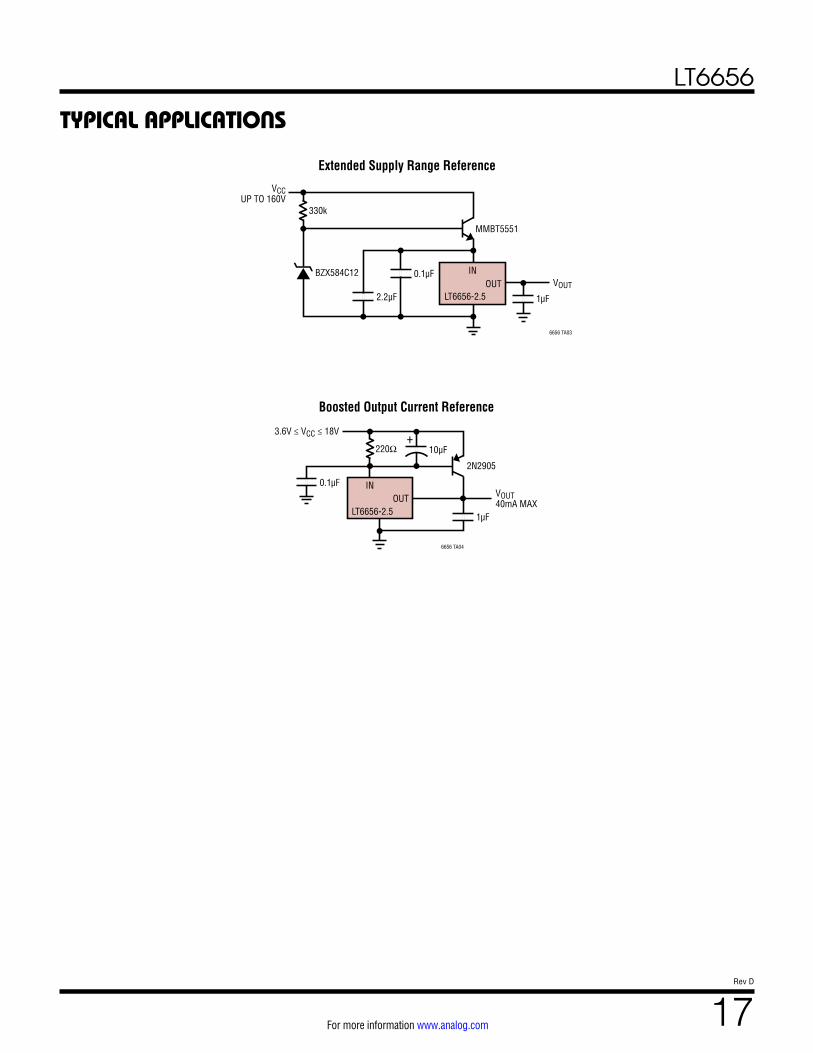
Boosted Output Current Reference
1µF
220Ω
6656 TA04
10µF
3.6V ≤ VCC ≤ 18V
VOUT40mA MAX
2N2905
+
OUTLT6656-2.5
IN0.1µF
Extended Supply Range Reference
VCCUP TO 160V
VOUT2.2µF 1µF
MMBT5551
6656 TA03
0.1µF
330k
BZX584C12OUT
LT6656-2.5
IN

LT6656
18Rev D
For more information www.analog.com
TYPICAL APPLICATIONS
Micropower Regulator, IQ = 2µA, Sink Up to 8mA
0.1µF
3V ≤ VCC ≤ 18V
2.5V1µF
6656 TA06
LT6656-2.5IN OUT
–
+LT6003
ADC Reference and Bridge Excitation Supply
0.1µF
3.8V ≤ VIN ≤ 18V
1µF
0.1µF 10µF
LT6656-3.3IN OUT
0.1µF
0.1µFCS
SCK
SDO
IN–
IN+
VREF VCC
LTC2452
10k10k
10k
3.3V ≤ VCC ≤ 5.5V
LT6656
19Rev D
For more information www.analog.com
TYPICAL APPLICATIONS
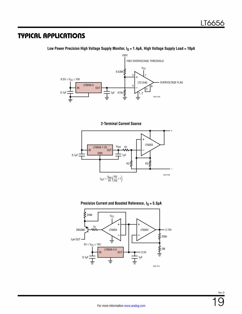
Low Power Precision High Voltage Supply Monitor, IQ = 1.4µA, High Voltage Supply Load = 10µA
0.1µF
6.5V ≤ VCC ≤ 10V
VCC
1µF
LT6656-5IN OUT
OVERVOLTAGE FLAG
6656 TA08
–
+LTC1540
7
56
3
4
1, 2
100V
105V OVERVOLTAGE THRESHOLD
9.53M
475k
2-Terminal Current Source
0.1µF 1µF
LT6656-1.25
GNDIN OUT
6656 TA09
–
+LT6003
–
+
R2
R1VREF
R3
IVR
RROUT
REF= +
1
23
1
Precision Current and Boosted Reference, IQ = 5.5µA
0.1µF 1µF
LT6656-2.5IN OUT
2.75V
3V ≤ VCC ≤ 16V
6656 TA10
–
+LT6004
–
+LT6004
200k
249k
1k
2M2.5V
1µA OUT
VCC
2N5086

LT6656
20Rev D
For more information www.analog.com
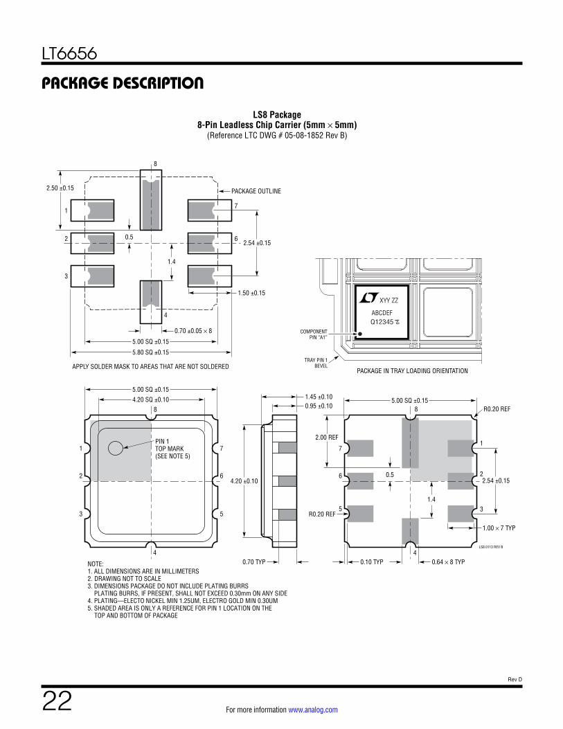
PACKAGE DESCRIPTION
1.50 – 1.75(NOTE 4)
2.80 BSC
0.30 – 0.45 6 PLCS (NOTE 3)
DATUM ‘A’
0.09 – 0.20(NOTE 3) S6 TSOT-23 0302
2.90 BSC(NOTE 4)
0.95 BSC
1.90 BSC
0.80 – 0.90
1.00 MAX0.01 – 0.10
0.20 BSC
0.30 – 0.50 REF
PIN ONE ID
NOTE:1. DIMENSIONS ARE IN MILLIMETERS2. DRAWING NOT TO SCALE3. DIMENSIONS ARE INCLUSIVE OF PLATING4. DIMENSIONS ARE EXCLUSIVE OF MOLD FLASH AND METAL BURR5. MOLD FLASH SHALL NOT EXCEED 0.254mm6. JEDEC PACKAGE REFERENCE IS MO-193
3.85 MAX
0.62MAX
0.95REF
RECOMMENDED SOLDER PAD LAYOUTPER IPC CALCULATOR
1.4 MIN2.62 REF
1.22 REF
S6 Package6-Lead Plastic TSOT-23
(Reference LTC DWG # 05-08-1636)

LT6656
21Rev D
For more information www.analog.com
PACKAGE DESCRIPTION
2.00 ±0.10(4 SIDES)
NOTE:1. DRAWING TO BE MADE A JEDEC PACKAGE OUTLINE M0-229 VARIATION OF (WCCD-2)2. DRAWING NOT TO SCALE3. ALL DIMENSIONS ARE IN MILLIMETERS4. DIMENSIONS OF EXPOSED PAD ON BOTTOM OF PACKAGE DO NOT INCLUDE MOLD FLASH. MOLD FLASH, IF PRESENT, SHALL NOT EXCEED 0.15mm ON ANY SIDE5. EXPOSED PAD SHALL BE SOLDER PLATED 6. SHADED AREA IS ONLY A REFERENCE FOR PIN 1 LOCATION ON THE TOP AND BOTTOM OF PACKAGE
0.40 ±0.10
BOTTOM VIEW—EXPOSED PAD
0.60 ±0.10(2 SIDES)
0.75 ±0.05
R = 0.125TYP
R = 0.05TYP
1.37 ±0.10(2 SIDES)
13
64
PIN 1 BARTOP MARK
(SEE NOTE 6)
0.200 REF
0.00 – 0.05
(DC6) DFN REV C 0915
0.25 ±0.050.50 BSC
0.25 ±0.05
1.37 ±0.10(2 SIDES)
RECOMMENDED SOLDER PAD PITCH AND DIMENSIONS
0.60 ±0.10(2 SIDES)
1.15 ±0.05
0.70 ±0.05
2.55 ±0.05
PACKAGEOUTLINE
0.50 BSC
PIN 1 NOTCH R = 0.20 OR 0.25 × 45° CHAMFER
DC6 Package6-Lead Plastic DFN (2mm × 2mm)
(Reference LTC DWG # 05-08-1703 Rev C)
LT6656
22Rev D
For more information www.analog.com
PACKAGE DESCRIPTION
7
8
1
3
4
2
2.00 REF
R0.20 REF
6
5
7
8
6
5
1
2
3
4
4.20 ±0.10
4.20 SQ ±0.10
2.54 ±0.15
1.00 × 7 TYP
0.64 × 8 TYP
LS8 0113 REV B
R0.20 REF
0.95 ±0.101.45 ±0.10
0.10 TYP0.70 TYP
1
4
7
8
6
1.4
0.5
1.50 ±0.15
2.50 ±0.15
2.54 ±0.15
0.70 ±0.05 × 8
PACKAGE OUTLINE
0.5
5.00 SQ ±0.15
5.00 SQ ±0.15
5.00 SQ ±0.15
5.80 SQ ±0.15
APPLY SOLDER MASK TO AREAS THAT ARE NOT SOLDERED
NOTE:1. ALL DIMENSIONS ARE IN MILLIMETERS2. DRAWING NOT TO SCALE3. DIMENSIONS PACKAGE DO NOT INCLUDE PLATING BURRS PLATING BURRS, IF PRESENT, SHALL NOT EXCEED 0.30mm ON ANY SIDE4. PLATING—ELECTO NICKEL MIN 1.25UM, ELECTRO GOLD MIN 0.30UM5. SHADED AREA IS ONLY A REFERENCE FOR PIN 1 LOCATION ON THE TOP AND BOTTOM OF PACKAGE
PIN 1TOP MARK(SEE NOTE 5)
2
3
LS8 Package8-Pin Leadless Chip Carrier (5mm × 5mm)
(Reference LTC DWG # 05-08-1852 Rev B)
ABCDEF
XYY ZZ
e4Q12345
TRAY PIN 1BEVEL
PACKAGE IN TRAY LOADING ORIENTATION
COMPONENTPIN “A1”
1.4
LT6656
23Rev D
For more information www.analog.com
Information furnished by Analog Devices is believed to be accurate and reliable. However, no responsibility is assumed by Analog Devices for its use, nor for any infringements of patents or other rights of third parties that may result from its use. Specifications subject to change without notice. No license is granted by implication or otherwise under any patent or patent rights of Analog Devices.
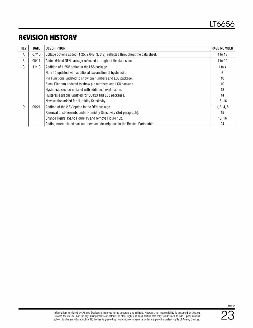
REVISION HISTORYREV DATE DESCRIPTION PAGE NUMBER
A 07/10 Voltage options added (1.25, 2.048, 3, 3.3), reflected throughout the data sheet. 1 to 18
B 05/11 Added 6-lead DFN package reflected throughout the data sheet. 1 to 20
C 11/13 Addition of 1.25V option in the LS8 package.Note 10 updated with additional explanation of hysteresis.Pin Functions updated to show pin numbers and LS8 package.Block Diagram updated to show pin numbers and LS8 package.Hysteresis section updated with additional explanation.Hysteresis graphs updated for SOT23 and LS8 packages.New section added for Humidity Sensitivity.
1 to 46
10101314
15, 16
D 05/21 Additon of the 2.8V option in the DFN package.Removal of statements under Humidity Sensitivity (3rd paragraph).Change Figure 15a to Figure 15 and remove Figure 15b.Adding more related part numbers and descriptions in the Related Parts table.
1, 3, 4, 515
15, 1624

LT6656
24Rev D
For more information www.analog.com ANALOG DEVICES, INC. 2010-2020
05/20www.analog.com
RELATED PARTSPART NUMBER DESCRIPTION COMMENTS
LT1389 Nanopower Precision Shunt Voltage Reference 0.05% Max 10ppm/°C Max, 800nA Supply
LTC1440 Micropower Comparator with Reference 3.7µA Max Supply Current, 1% 1.182V Reference, MSOP, PDIP and SO-8 Packages
LT1460 Micropower Series Reference 0.075% Max, 10ppm/°C Max Drift, 2.5V, 5V and 10V Versions, MSOP, PDIP, SO-8, SOT-23 and TO-92 Packages
LT1461 Micropower Precision LDO Series Reference 3ppm/°C Max Drift, 0°C to 70°C, –40°C to 85°C, –40°C to 125°C Options in SO-8
LT1495 1.5µA Precision Rail-to-Rail Dual Op Amp 1.5µA Max Supply Current, 100pA Max IOS
LTC1540 Nanopower Comparator with Reference 600nA Max Supply Current, 2% 1.182V Reference, MSOP and SO-8 Packages
LT1634 Micropower Precision Shunt Voltage Reference
0.05% Max, 10ppm/°C Max Drift, 1.25V, 2.5V, 4.096V, 5V, 10µA Maximum Supply Current
LT1790 Micropower Precision Series Reference 0.05% Max, 10ppm/°C Max, 60µA Supply, SOT23 Package
LTC1798 6µA Low Dropout Series Reference Available in Adjustable, 2.5V, 3V, 4.096V and 5V
LT6003 1.6V, 1µA Precision Rail-to-Rail Op Amp 1µA Max Supply Current, 1.6V Minimum Operating Voltage, SOT-23 and DFN Packages
LT6650 Micropower Reference with Buffer Amplifier 0.05% Max, 5.6µA Supply, SOT-23 Package
LT6660 Tiny Micropower Series Reference 0.2% Max, 20ppm/°C Max, 20mA Output Current, 2mm × 2mm DFN
LT6700 Micropower, Low Voltage Dual Comparator with 40mV Reference
6.5µA Supply Current, 1.4V Minimum Operating Voltage
ADR3425 Micropower, High-Accuracy Voltage Reference 100µA Supply Current, ±0.1% Max Initial Accuracy, 8ppm/°C Max drift
ADR3525 Micropower, Precision, Auto Qualified Voltage Reference
AEC-Q100, 100µA Supply Current, ±0.1% Max Initial Accuracy, 5ppm/°C B-Grade Max Drift
ADR5041 Precision Micropower Shunt Mode Voltage Reference
AEC-Q100, SC70 or SOT-23 Package, 50µA to 15mA Supply Current, No External Capacitor Required
AD4000/AD4001
16-Bit, 2Msps Precision Pseudo Differential or Differential SAR ADC
INL: ±1.0LSB Maximum; 7mW/Msps, 70µW at 10ksps, 14mW at 2Msps from VDD Only
LTC2376-16/LTC2378-16
18-Bit, 250ksps, Low Power SAR ADC with 102dB SNR
±1.75LSB INL (Max), 2.5V Supply, 3.4mW at 250ksps
LTC2400 24-Bit µPower No Latency ∆∑™ ADC in SO-8 200µA Supply Current, 12.5% Overrange and Underrange, 50Hz/60Hz Notch Filter with 110dB Min Attenuation
AD7980 16-Bit, 1Msps, PulSAR ADC in MSOP/LFCSP INL: ±0.6LSB Typ, ±1.25LSB Max, 2.5V Supply with 1.8V/2.5V/3V/5V Logic Interface, 4mW at 1Msps (VDD Only)
AD4695/AD4696
16-Channel 16-Bit 500ksps SAR ADC 8mW at fs = 1Msps (AD4696), 4mW at fs = 500ksps (AD4695 and AD4696)
TYPICAL APPLICATIONReference Regulator for Micropower DAC, Total IQ = 4.8µA
0.1µF
5.1V ≤ VIN ≤ 18V
10µF
VREF VCC
GND
CSSCKSDI
LTC1662
DAC A
DAC B
LT6656-5IN OUT
5V
0V TO 5V OUTPUT
0V TO 5V OUTPUT
6656 TA07