lt8708 (rev. 0) - analog.com · lt8708 4 rev 0 for more information electrical characteristics the...
TRANSCRIPT

LT8708
1Rev 0
For more information www.analog.com
VBAT2 = 13.5VIOUT = 15A
VBAT1 (V)10 12 14 16
94
95
96
97
98
99
100
EFFI
CIEN
CY (%
)
EFFICIENCY
8708 TA01b
+
–
+
–
CSPOUT
CSNOUTEXTVCC
VOUTLOMONFBOUTINTVCC
GATEVCC
IMON_ONIMON_OP
ICNICP
IMON_INPIMON_INN
CLKOUTSYNCSSRTVCMODE
CSNINTG1 BOOST1 SW1 BG1 CSP CSN
LT8708
GND BG2 SW2 BOOST2 TG2
CSPINVINCHIPSHDNFBINVINHIMON
SWENLDO33
DIR
RVSOFF
126kHz
FWD (3V)RVS (0V)
++
DB1 DB2
TOBOOST1
TOBOOST2
ILIM
TO DIODE DB1
LD033
VBAT2
8708 TA01a
ILIM
10V TO 16VBATTERY
VBAT1
10V TO 16V
BATTERY TO DIODE DB2
POWER TRANSFERDECISION LOGIC
TYPICAL APPLICATION
FEATURES DESCRIPTION
80V Synchronous 4-Switch Buck-Boost DC/DC Controller with Flexible Bidirectional Capability
The LT®8708 is a high performance buck-boost switching regulator controller that operates from an input voltage that can be above, below or equal to the output voltage. Features are included to simplify bidirectional power conversion in battery/capacitor backup systems and other applications that may need regulation of VOUT, VIN, IOUT, and/or IIN. Forward and reverse current can be monitored and limited for the input and output sides of the converter. All four current limits (forward input, reverse input, forward output and reverse output) can be set independently using four resistors on the PCB.
The MODE pin can select between discontinuous conduc-tion mode (DCM), continuous conduction mode (CCM), hybrid conduction mode (HCM) and Burst Mode® operation. In combination with the DIR (direction) pin, the chip can be configured to process power only from VIN to VOUT or only from VOUT to VIN. With a wide 2.8V to 80V input and 1.3V to 80V output range, the LT8708 is compatible with most solar, automotive, telecom and battery-powered systems.
12V Bidirectional Dual Battery System with FHCM and RHCM
APPLICATIONS
n Single Inductor Allows VIN Above, Below, or Equal to VOUT
n Six Independent Forms of Regulation n VIN Current (Forward and Reverse) n VOUT Current (Forward and Reverse) n VIN and VOUT Voltage
n Forward and Reverse Discontinuous Conduction Mode Supported
n Supports MODE and DIR Pin Changes While Switching n VINCHIP Range 2.8V (Need EXTVCC > 6.4V) to 80V n VOUT Range: 1.3V to 80V n Synchronous Rectification: Up to 99% Efficiency n Available in 40-Lead (5mm × 8mm) QFN with High
Voltage Pin Spacing
n High Voltage Buck-Boost Converters n Bidirectional Charging System n Automotive 48V Systems
All registered trademarks and trademarks are the property of their respective owners.
Efficiency
Document Feedback
LT8708
2Rev 0
For more information www.analog.com
TABLE OF CONTENTS Features ..................................................... 1Applications ................................................ 1Typical Application ........................................ 1Description.................................................. 1Absolute Maximum Ratings .............................. 3Order Information .......................................... 3Pin Configuration .......................................... 3Electrical Characteristics ................................. 4Typical Performance Characteristics ................... 9Typical Performance Characteristics .................. 11Pin Functions .............................................. 13Block Diagram ............................................. 15Operation................................................... 16
Typographical Conventions ..................................... 16Start-Up .................................................................. 16
Start-Up: SHDN Pin ............................................ 16Start-Up: SWEN Pin ............................................ 16Start-Up: Soft-Start of Switching Regulator ....... 17
Control Overview .................................................... 17Power Switch Control ............................................ 18
Switch Control: Buck Region (VIN >> VOUT) ....... 19Switch Control: Buck-Boost (VIN ≅ VOUT) ......... 19Switch Control: Boost Region (VIN << VOUT) ......20Switch Control: Soft-Start ..................................20
Uni and Bidirectional Conduction ............................20Bidirectional Conduction: CCM .......................... 21Unidirectional Conduction: DCM ......................... 21Unidirectional Conduction: HCM .........................22Unidirectional Conduction: Burst Mode ..............22
Error Amplifiers ......................................................22VOUT Regulation and Sensing .................................23
VOUT: Regulation .................................................23VOUT: Above Regulation ......................................23VOUT: Below Regulation and Undervoltage .........23
VIN Regulation and Sensing .................................... 24VIN: Regulation ................................................... 24VIN: Above Regulation and Overvoltage .............. 24VIN: Below Regulation ......................................... 24
Current Monitoring and Limiting ............................. 24Monitoring and Limiting: IMON Pins .................. 24Monitoring: ICP and ICN Pins .............................25
INTVCC/EXTVCC/GATEVCC/LDO33 Power ...............25CLKOUT and Temperature Sensing .........................25
Applications Information ................................ 26Verify the Power Flow Conditions ...........................26Operating Frequency Selection ...............................26Internal Oscillator ...................................................27SYNC Pin and Clock Synchronization .....................27CLKOUT Pin and Clock Synchronization .................27Inductor Current Sensing and Slope Compensation .... 27RSENSE Selection and Maximum Current ................28
RSENSE Selection: Max RSENSE in the Boost Region ......................................................28RSENSE Selection: Max RSENSE in the Buck Region .......................................................30RSENSE Selection: Final RSENSE Value ................. 31
RSENSE Filtering ......................................................32Inductor (L) Selection ............................................32
L Selection: Load Current in Buck and Boost Regions ....................................................32L Selection: Subharmonic Oscillations ...............33L Selection: Maximum Current Rating ................33
Power MOSFET Selection .......................................34CIN and COUT Selection ........................................... 37Schottky Diode (D1, D2, D3, D4) Selection .............38Topside MOSFET Driver Supply (CB1, DB1, CB2, DB2) ... 39
Top Driver: Boost Cap Charge Control Block ......39Top Driver: Boost Diodes DB1 and DB2 ................... 39
VINHIMON, VOUTLOMON and RVSOFF ..................39IIN and IOUT Current Monitoring and Limiting .........42Loop Compensation ................................................44INTVCC Regulators and EXTVCC Connection ...........45LDO33 Regulator ....................................................45Voltage Lockouts ....................................................46Junction Temperature Measurement ......................46Thermal Shutdown ................................................. 47Efficiency Considerations ...................................... 47Circuit Board Layout Checklist ............................... 47Hot Plugging Considerations .................................49Design Example ......................................................49
Typical Applications ...................................... 55Package Description ..................................... 63Typical Application ....................................... 64Related Parts .............................................. 64

LT8708
3Rev 0
For more information www.analog.com
PIN CONFIGURATIONABSOLUTE MAXIMUM RATINGS
VCSP – VCSN, VCSPIN – VCSNIN, VCSPOUT – VCSNOUT ............................... –0.3V to 0.3V
CSP, CSN Voltage ......................................... –0.3V to 3VVC Voltage (Note 2) .................................. –0.3V to 2.2VRT, FBOUT, SS Voltage ................................ –0.3V to 5VIMON_INP, IMON_INN, IMON_OP, IMON_ON,
ICP, ICN Voltage ....................................... –0.3V to 5VSYNC Voltage ............................................ –0.3V to 5.5VINTVCC, GATEVCC Voltage ............................ –0.3V to 7VVBOOST1 – VSW1, VBOOST2 – VSW2 ................ –0.3V to 7VSWEN, RVSOFF Voltage ............................... –0.3V to 7VSWEN Current .......................................................0.5mARVSOFF Current .......................................................1mAFBIN, SHDN Voltage .................................. –0.3V to 30VVINHIMON Voltage ..................................... –0.3V to 30VVOUTLOMON Voltage .................................. –0.3V to 5VDIR, MODE Voltage ...................................... –0.3V to 5VCSNIN, CSPIN, CSPOUT, CSNOUT Voltage –0.3V to 80VVINCHIP, EXTVCC Voltage ............................ –0.3V to 80VSW1, SW2 Voltage ..................................... 81V (Note 6)BOOST1, BOOST2 Voltage ......................... –0.3V to 87VBG1, BG2, TG1, TG2 .......................................... (Note 5)LDO33, CLKOUT ............................................... (Note 8)Operating Junction Temperature Range
LT8708E (Notes 3, 8) ........................ –40°C to 125°C LT8708I (Notes 3, 8) ......................... –40°C to 125°C LT8708H (Notes 3, 8) ....................... –40°C to 150°CStorage Temperature Range .................. –65°C to 150°C
(Note 1)
15 16 17 18
TOP VIEW
41GND
UHG PACKAGE40-LEAD (5mm × 8mm) PLASTIC QFN
TJMAX = 150°C, θJA = 36°C/W, θJC = 3.8°C/WEXPOSED PAD (PIN 41) IS GND, MUST BE SOLDERED TO PCB
19 20 21
40 39 38 37 36 35 34
26
27
28
29
3031
32
33
8
7
6
5
4
3
2
1CLKOUT
SS
SHDN
CSN
CSP
ICN
DIR
FBIN
FBOUT
VC
IMON_INP
IMON_INN
RT
SYNC
CSPIN
CSNIN
CSNOUT
CSPOUT
EXTVCC
ICP
VINHIMON
VOUTLOMON
RVSOFF
BOOST1
TG1
SW1
LDO3
3
IMON
_ON
IMON
_OP
MOD
E
SWEN
INTV
CC
V INC
HIP
GND
BG1
GATE
V CC
BG2
BOOS
T2 TG2
SW2
25
24
23
22
9
10
11
12
13
14
ORDER INFORMATIONLEAD FREE FINISH TAPE AND REEL PART MARKING* PACKAGE DESCRIPTION TEMPERATURE RANGE
LT8708EUHG#PBF LT8708EUHG#TRPBF 8708 40-Lead (5mm × 8mm) Plastic QFN –40°C to 125°C
LT8708IUHG#PBF LT8708IUHG#TRPBF 8708 40-Lead (5mm × 8mm) Plastic QFN –40°C to 125°C
LT8708HUHG#PBF LT8708HUHG#TRPBF 8708 40-Lead (5mm × 8mm) Plastic QFN –40°C to 150°C
Consult ADI Marketing for parts specified with wider operating temperature ranges. *The temperature grade is identified by a label on the shipping container.
Tape and reel specifications. Some packages are available in 500 unit reels through designated sales channels with #TRMPBF suffix.

LT8708
4Rev 0
For more information www.analog.com
ELECTRICAL CHARACTERISTICS The l denotes the specifications which apply over the full operating temperature range, otherwise specifications are at TA = 25°C. VINCHIP = 12V, SHDN = 3V, DIR = 3.3V unless otherwise noted (Note 3).
PARAMETER CONDITIONS MIN TYP MAX UNITS
Voltage Supplies and Regulators
VINCHIP Operating Voltage Range EXTVCC = 0V EXTVCC = 7.5V
l
l
5.5 2.8
80 80
V V
VINCHIP Quiescent Current Not Switching, VEXTVCC = 0V SWEN = 3.3V SWEN = 0V
3.9
2.45
6.5 4.5
mA mA
VINCHIP Quiescent Current in Shutdown VSHDN = 0V 0 1 μA
EXTVCC Switchover Voltage IINTVCC = –20mA, VEXTVCC Rising l 6.15 6.4 6.6 V
EXTVCC Switchover Hysteresis 0.2 V
INTVCC Current Limit Maximum Current Draw from INTVCC and LDO33 Pins Combined. Regulated from VINCHIP or EXTVCC (12V) INTVCC = 5.25V INTVCC = 4.4V
l
l
90 28
127 42
165 55
mA mA
INTVCC Voltage Regulated from VINCHIP, IINTVCC = 20mA Regulated from EXTVCC (12V), IINTVCC = 20mA
l
l
6.1 6.1
6.3 6.3
6.5 6.5
V V
INTVCC Load Regulation IINTVCC = 0mA to 50mA –0.5 –1.5 %
INTVCC, GATEVCC Undervoltage Lockout INTVCC Falling, GATEVCC Connected to INTVCC l 4.45 4.65 4.85 V
INTVCC, GATEVCC Undervoltage Lockout Hysteresis GATEVCC Connected to INTVCC 170 mV
INTVCC Regulator Dropout Voltage VINCHIP – VINTVCC, IINTVCC = 20mA 220 mV
LDO33 Pin Voltage 5mA from LDO33 Pin l 3.23 3.295 3.35 V
LDO33 Pin Load Regulation ILDO33 = 0.1mA to 5mA –0.25 –1 %
LDO33 Pin Current Limit SYNC = 3V l 12 17.25 22 mA
LDO33 Pin Undervoltage Lockout LDO33 Falling 2.96 3.04 3.12 V
LDO33 Pin Undervoltage Lockout Hysteresis 35 mV
Switching Regulator Control
Maximum Current Sense Threshold (VCSP – VCSN) Boost Mode, Minimum M3 Switch Duty Cycle l 76 93 110 mV
Maximum Current Sense Threshold (VCSN – VCSP) Buck Mode, Minimum M2 Switch Duty Cycle l 68 82 97 mV
Maximum Current Sense Threshold (VCSN – VCSP) Boost Mode, Minimum M3 Switch Duty Cycle l 79 93 108 mV
Maximum Current Sense Threshold (VCSP – VCSN) Buck Mode, Minimum M2 Switch Duty Cycle l 72 84 96 mV
Gain from VC to Maximum Current Sense Voltage (VCSP – VCSN) (A5 in the Block Diagram)
Boost Mode Buck Mode
135 –135
mV/V mV/V
SHDN Input Voltage High SHDN Rising to Enable the Device l 1.175 1.221 1.275 V
SHDN Input Voltage High Hysteresis 40 mV
SHDN Input Voltage Low Device Disabled, Low Quiescent Current (LT8708E, LT8708I) (LT8708H)
l
l
0.35 0.3
V V
SHDN Pin Bias Current VSHDN = 3V VSHDN = 12V
0 14
1 22
μA μA
SWEN Rising Threshold Voltage l 1.156 1.208 1.256 V
SWEN Threshold Voltage Hysteresis 22 mV
SWEN Output Voltage Low ISWEN = 200μA SHDN = 0V or VINCHIP = 0V SHDN = 3V
l
l
0.9 0.2
1.1 0.5
V V

LT8708
5Rev 0
For more information www.analog.com
PARAMETER CONDITIONS MIN TYP MAX UNITS
SWEN Internal Pull-Down Release Voltage SHDN = 3V l 0.75 0.8 V
MODE Pin Continuous Conduction Mode (CCM) Threshold
l 0.4 V
MODE Pin Hybrid DCM/CCM Mode (HCM) Range l 0.8 1.2 V
MODE Pin Discontinuous Conduction Mode (DCM) Range
l 1.6 2.0 V
MODE Pin Burst Mode Operation Threshold l 2.4 V
DIR Pin Forward Operation Threshold l 1.6 V
DIR Pin Reverse Operation Threshold l 1.2 V
RVSOFF Output Voltage Low IRVSOFF = 200μA l 0.08 0.5 V
RVSOFF Falling Threshold Voltage l 1.155 1.209 1.275 V
RVSOFF Threshold Voltage Hysteresis 165 mV
Soft-Start Charging Current VSS = 0V 13 19 25 μA
ICN Rising Threshold for FDCM Operation MODE = 1V (HCM), DIR = 3.3V l 235 255 280 mV
ICN Falling Threshold for CCM Operation MODE = 1V (HCM), DIR = 3.3V l 185 205 235 mV
IMON_INP Rising Threshold for RDCM Operation MODE = 1V (HCM), DIR = 0V l 235 255 280 mV
IMON_INP Falling Threshold for CCM Operation MODE = 1V (HCM), DIR = 0V l 185 205 235 mV
Voltage Regulation Loops (Refer to Block Diagram to Locate Amplifiers)
Regulation Voltage for FBOUT Regulate VC to 1.2V l 1.193 1.207 1.222 V
Regulation Voltage for FBIN Regulate VC to 1.2V l 1.184 1.205 1.226 V
Line Regulation for FBOUT and FBIN Error Amp Reference Voltage
VINCHIP = 12V to 80V. Not Switching 0.002 0.005 %/V
FBOUT Pin Bias Current Current Out of Pin 15 nA
FBOUT Error Amp EA4 gm 345 μmho
FBOUT Error Amp EA4 Voltage Gain 245 V/V
VOUTLOMON Voltage Activation Threshold Falling l 1.185 1.207 1.225 V
VOUTLOMON Threshold Voltage Hysteresis 24 mV
VOUTLOMON Pin Bias Current VVOUTLOMON =1.24V, Current Into Pin VVOUTLOMON =1.17V, Current Into Pin
l
0.8
0.01 1
1.2
μA μA
FBIN Pin Bias Current Current Out of Pin 10 nA
FBIN Error Amp EA3 gm 235 μmho
FBIN Error Amp EA3 Voltage Gain 150 V/V
VINHIMON Voltage Activation Threshold Rising l 1.185 1.207 1.23 V
VINHIMON Threshold Voltage Hysteresis 24 mV
VINHIMON Pin Bias Current VVINHIMON = 1.17V, Current Out of Pin VVINHIMON = 1.24V, Current Out of Pin
l
0.8
0.03 1
1.2
μA μA
Current Regulation Loops (Refer to Block Diagram to Locate Amplifiers)
Regulation Voltages for IMON_INP and IMON_OP VC = 1.2V l 1.185 1.209 1.231 V
Regulation Voltages for IMON_INN and IMON_ON VC =1.2V l 1.185 1.21 1.24 V
ELECTRICAL CHARACTERISTICS The l denotes the specifications which apply over the full operating temperature range, otherwise specifications are at TA = 25°C. VINCHIP = 12V, SHDN = 3V, DIR = 3.3V unless otherwise noted (Note 3).

LT8708
6Rev 0
For more information www.analog.com
PARAMETER CONDITIONS MIN TYP MAX UNITS
Line Regulation for IMON_INP, IMON_INN, IMON_OP and IMON_ON Error Amp Reference Voltage
VINCHIP = 12V to 80V 0.002 0.005 %/V
CSPIN Bias Current VCSPIN = 12V VCSPIN = 1.5V
0.01 0.01
μA μA
CSNIN Bias Current BOOST Capacitor Charge Control Block Not Active VSWEN = 3.3V, VCSPIN = VCSNIN = 12V VSWEN = 3.3V, VCSPIN = VCSNIN = 1.5V VSWEN = 0V
84
4.25 0.01
μA μA μA
CSPIN, CSNIN Common Mode Operating Voltage Range
l 0 80 V
CSPIN, CSNIN Differential Mode Operating Voltage Range
l –100 100 mV
IMON_INP Output Current VCSPIN – VCSNIN = 50mV, VCSNIN = 5V VCSPIN – VCSNIN = 50mV, VCSNIN = 5V VCSPIN – VCSNIN = 5mV, VCSNIN = 5V VCSPIN – VCSNIN = 5mV, VCSNIN = 5V
l
l
67 64.5 22.5 20
70 70 25 25
73 75.5 27.5 30
μA μA μA μA
IMON_INN Output Current VCSNIN – VCSPIN = 50mV, VCSNIN = 5V VCSNIN – VCSPIN = 50mV, VCSNIN = 5V VCSNIN – VCSPIN = 5mV, VCSNIN = 5V VCSNIN – VCSPIN = 5mV, VCSNIN = 5V
l
l
66 65 19 18
70 70 25 25
74 75
30.5 32
μA μA μA μA
IMON_INP and IMON_INN Max Output Current l 120 μA
IMON_INP Error Amp EA5 gm 190 μmho
IMON_INP Error Amp EA5 Voltage Gain 130 V/V
IMON_INN Error Amp EA1 gm FBIN = 0V, FBOUT = 3.3V 190 μmho
IMON_INN Error Amp EA1 Voltage Gain FBIN = 0V, FBOUT = 3.3V 130 V/V
CSPOUT Bias Current VCSPOUT = 12V VCSPOUT = 1.5V
0.01 0.01
μA μA
CSNOUT Bias Current BOOST Capacitor Charge Control Block Not Active VSWEN = 3.3V, VCSPOUT = VCSNOUT = 12V VSWEN = 3.3V, VCSPOUT = VCSNOUT = 1.5V VSWEN = 0V
83
4.25 0.01
μA μA μA
CSPOUT, CSNOUT Common Mode Operating Voltage Range
l 0 80 V
CSPOUT, CSNOUT Differential Mode Operating Voltage Range
l –100 100 mV
IMON_OP, ICP Output Current VCSPOUT – VCSNOUT = 50mV, VCSNOUT = 5V VCSPOUT – VCSNOUT = 50mV, VCSNOUT = 5V VCSPOUT – VCSNOUT = 5mV, VCSNOUT = 5V VCSPOUT – VCSNOUT = 5mV, VCSNOUT = 5V VCSPOUT – VCSNOUT = –5mV, VCSNOUT = 5V VCSPOUT – VCSNOUT = –5mV, VCSNOUT = 5V
l
l
l
67 65
22.5 20.5 12.5 10.5
70 70 25 25 15 15
73 76
27.5 29
17.5 19.5
μA μA μA μA μA μA
IMON_ON, ICN Output Current VCSNOUT – VCSPOUT = 50mV, VCSNOUT = 5V VCSNOUT – VCSPOUT = 50mV, VCSNOUT = 5V VCSNOUT – VCSPOUT = 5mV, VCSNOUT = 5V VCSNOUT – VCSPOUT = 5mV, VCSNOUT = 5V VCSNOUT – VCSPOUT = –5mV, VCSNOUT = 5V VCSNOUT – VCSPOUT = –5mV, VCSNOUT = 5V
l
l
l
67 65
22.5 20.5 12.5 10.5
70 70 25 25 15 15
73 75
27.5 29
17.5 19.5
μA μA μA μA μA μA
ELECTRICAL CHARACTERISTICS The l denotes the specifications which apply over the full operating temperature range, otherwise specifications are at TA = 25°C. VINCHIP = 12V, SHDN = 3V, DIR = 3.3V unless otherwise noted (Note 3).

LT8708
7Rev 0
For more information www.analog.com
PARAMETER CONDITIONS MIN TYP MAX UNITS
IMON_OP, IMON_ON, ICP and ICN Max Output Current
l 120 μA
IMON_OP Error Amp EA6 gm 190 μmho
IMON_OP Error Amp EA6 Voltage Gain 130 V/V
IMON_ON Error Amp EA2 gm FBIN = 0V, FBOUT = 3.3V 190 μmho
IMON_ON Error Amp EA2 Voltage Gain FBIN = 0V, FBOUT = 3.3V 130 V/V
NMOS Gate Drivers
TG1, TG2 Rise Time CLOAD = 3300pF (Note 4) 20 ns
TG1, TG2 Fall Time CLOAD = 3300pF (Note 4) 20 ns
BG1, BG2 Rise Time CLOAD = 3300pF (Note 4) 20 ns
BG1, BG2 Fall Time CLOAD = 3300pF (Note 4) 20 ns
TG1 Off to BG1 On Delay CLOAD = 3300pF Each Driver 90 ns
BG1 Off to TG1 On Delay CLOAD = 3300pF Each Driver 80 ns
TG2 Off to BG2 On Delay CLOAD = 3300pF Each Driver 90 ns
BG2 Off to TG2 On Delay CLOAD = 3300pF Each Driver 80 ns
Minimum On-Time for Main Switch in Boost Operation (tON(M3,MIN))
Switch M3, CLOAD = 3300pF 200 ns
Minimum On-Time for Synchronous Switch in Buck Operation (tON(M2,MIN))
Switch M2, CLOAD = 3300pF 200 ns
Minimum Off-Time for Main Switch in Steady-State Boost Operation
Switch M3, CLOAD = 3300pF 230 ns
Minimum Off-Time for Synchronous Switch in Steady-State Buck Operation
Switch M2, CLOAD = 3300pF 230 ns
Oscillator
Switch Frequency Range SYNCing or Free Running 100 400 kHz
Switching Frequency, FOSC RT = 365k RT = 215k RT = 124k
l
l
l
102 170 310
120 202 350
142 235 400
kHz kHz kHz
SYNC High Level for Synchronization l 1.3 V
SYNC Low Level for Synchronization l 0.5 V
SYNC Clock Pulse Duty Cycle VSYNC = 0V to 2V 20 80 %
Recommended Min SYNC Ratio FSYNC/FOSC 3/4
CLKOUT Output Voltage High VLDO33 – VCLKOUT, 1mA Out of CLKOUT Pin, ILDO33 = 0μA
100 250 mV
CLKOUT Output Voltage Low 1mA Into CLKOUT Pin 25 100 mV
CLKOUT Duty Cycle TJ = –40°C TJ = 25°C TJ = 125°C
22.7 44.1 77
% % %
ELECTRICAL CHARACTERISTICS The l denotes the specifications which apply over the full operating temperature range, otherwise specifications are at TA = 25°C. VINCHIP = 12V, SHDN = 3V, DIR = 3.3V unless otherwise noted (Note 3).

LT8708
8Rev 0
For more information www.analog.com
PARAMETER CONDITIONS MIN TYP MAX UNITS
CLKOUT Rise Time CLOAD = 200pF 20 ns
CLKOUT Fall Time CLOAD = 200pF 20 ns
CLKOUT Phase Delay SYNC Rising to CLKOUT Rising, fOSC = 100kHz l 160 180 200 degrees
Note 1: Stresses beyond those listed under Absolute Maximum Ratings may cause permanent damage to the device. Exposure to any Absolute Maximum Rating condition for extended periods may affect device reliability and lifetime.Note 2: Do not force voltage on the VC pin.Note 3: The LT8708E is guaranteed to meet performance specifications from 0°C to 125°C junction temperature. Specifications over the –40°C to 125°C operating junction temperature range are assured by design, characterization and correlation with statistical process controls. The LT8708I is guaranteed over the full –40°C to 125°C junction temperature range. The LT8708H is guaranteed over the full –40°C to 150°C operating junction temperature range.Note 4: Rise and fall times are measured using 10% and 90% levels. Delay times are measured using 50% levels.
Note 5: Do not apply a voltage or current source to these pins. They must be connected to capacitive loads only, otherwise permanent damage may occur.Note 6: Negative voltages on the SW1 and SW2 pins are limited, in an application, by the body diodes of the external NMOS devices, M2 and M3, or parallel Schottky diodes when present. The SW1 and SW2 pins are tolerant of these negative voltages in excess of one diode drop below ground, guaranteed by design.Note 7: This IC includes overtemperature protection that is intended to protect the device during momentary overload conditions. Junction temperature will exceed the maximum operating junction temperature when overtemperature protection is active. Continuous operation above the specified maximum operating junction temperature may impair device reliability.Note 8: Do not force voltage or current into these pins.
ELECTRICAL CHARACTERISTICS The l denotes the specifications which apply over the full operating temperature range, otherwise specifications are at TA = 25°C. VINCHIP = 12V, SHDN = 3V, DIR = 3V unless otherwise noted (Note 3).

LT8708
9Rev 0
For more information www.analog.com
TYPICAL PERFORMANCE CHARACTERISTICS
Efficiency vs Output Current (Boost Region – Page 59)
Efficiency vs Output Current (Buck Region – Page 59)
Efficiency vs Output Current (Buck–Boost Region – Page 59)
Feedback Voltages Feedback Voltages (Five Parts) Oscillator Frequency
Maximum Inductor Current Sense Voltage vs Duty Cycle
Inductor Current Sense Voltage at Minimum Duty Cycle
Maximum Inductor Current Sense Voltage at Minimum Duty Cycle
LOAD CURRENT (A)0.01 0.1 1 100
10
20
30
40
50
60
70
80
90
100
EFFI
CIEN
CY (
%)
8708 G01
HCMDCMCCM
VIN = 38VVOUT = 47.4V
LOAD CURRENT (A)0.01 0.1 1 100
10
20
30
40
50
60
70
80
90
100
EFFI
CIEN
CY (
%)
8708 G02
HCMDCMCCM
VIN = 51.5VVOUT = 47.4V
LOAD CURRENT (A)0.01 0.1 1 100
10
20
30
40
50
60
70
80
90
100
EFFI
CIEN
CY (
%)
8708 G03
HCMDCMCCM
VIN = 48VVOUT = 47.4V
VC = 1.2V
FBOUTFBINIMON_INPIMON_INNIMON_ONIMON_OP
TEMPERATURE (°C)–45 –20 5 30 55 80 105 130 155
1.17
1.18
1.19
1.20
1.21
1.22
1.23
PIN
VOLT
AGE
(V)
Feedback Voltages
8708 G04
VC = 1.2V
TEMPERATURE (°C)–45 –20 5 30 55 80 105 130 155
1.17
1.18
1.19
1.20
1.21
1.22
1.23
PIN
VOLT
AGE
(V)
8708 G05
RT = 124k
RT = 215k
RT = 365k
TEMPERATURE (°C)–45 –20 5 30 55 80 105 130 155
0
50
100
150
200
250
300
350
400
FREQ
UENC
Y (k
Hz)
Oscillator Frequency
8708 G06
BUCK REGION
BOOST REGION
M2 OR M3 DUTY CYCLE (%)0 20 40 60 80 100
0
20
40
60
80
100
120
140
|CSP
–CSN
| (m
V)
8708 G07
BUCK REGION
BOOST REGION
VC (V)0.5 1 1.5 2
–100
–80
–60
–40
–20
0
20
40
60
80
100
–100
–80
–60
–40
–20
0
20
40
60
80
100
CSN–
CSP
(mV)
CSP–CSN (mV)
8708 G08
BUCK REGION
BOOST REGION
TEMPERATURE (°C)–45 –20 5 30 55 80 105 130 155
0
20
40
60
80
100
120
|CSP
–CSN
| (m
V)
Voltage at Minimum Duty Cycle
8708 G09

LT8708
10Rev 0
For more information www.analog.com
TYPICAL PERFORMANCE CHARACTERISTICS
Minimum Inductor Current Sense Voltage vs Duty Cycle
INTVCC Line Regulation (EXTVCC = 0V)
Minimum Inductor Current Sense Voltage at Minimum Duty Cycle
Maximum and Minimum VC vs SSINTVCC Line Regulation (VIN = 12V) IMONx, ICx Output Current
CLKOUT Duty CycleLDO33 Pin Regulation (ILDO33 = 1mA)
VIN Supply Current vs Voltage (Not Switching)
BUCK REGION
BOOST REGION
M2 OR M3 DUTY CYCLE (%)0 20 40 60 80 100
–140
–120
–100
–80
–60
–40
–20
0
–|CS
P–CS
N| (
mV)
8708 G10VIN (V)
4 6 8 10 12 14 16 18 204.0
4.5
5.0
5.5
6.0
6.5
7.0
INTV
CC (V
)
8708 G11
BUCK REGION
BOOST REGION
TEMPERATURE (°C)–45 –20 5 30 55 80 105 130 155
–120
–100
–80
–60
–40
–20
0
–|CS
P–CS
N| (m
V)
8708 G12
BUCK REGION
BOOST REGION
MINIMUM VC
MAXIMUM VC
TJ = 25°C
SS (V)0 0.3 0.6 0.9 1.2 1.5
0
0.5
1.0
1.5
2.0
2.5
V C (V
)
Maximum and Minimum VC vs SS
8708 G13
EXTVCC RISING
EXTVCC FALLING
EXTVCC (V)4 6 8 10 12
5.5
6.0
6.5
7.0
INTV
CC (V
)
8708 G14CSPIN–CSNIN (mV)
CSPOUT–CSNOUT (mV)
–200 –100 0 100 200–25.0
0
25.0
50.0
75.0
100.0
125.0
150.0
175.0
200.0
225.0
250.0
IMON
X, IC
X CU
RREN
T (µ
A)
8708 G15
IMON_INNIMON_ONICN
IMON_INPIMON_OPICP
TEMPERATURE (°C)–45 –20 5 30 55 80 105 130 155
0
20
40
60
80
100
DUTY
CYC
LE (%
)
CLKOUT Duty Cycle
8708 G16
150°C–45°C25°C
INTVCC (V)2.5 3 3.5 4 4.5 5 5.5 6 6.5
1.5
2.0
2.5
3.0
3.5
LDO3
3 (V
)
8708 G17
150°C–45°C25°C
VIN (V)5 20 35 50 65 80
0
0.5
1.0
1.5
2.0
2.5
3.0
3.5
I IN (m
A)
8708 G18

LT8708
11Rev 0
For more information www.analog.com
SHDN Pin CurrentSHDN and SWEN Pin Thresholds vs Temperature
Internal VIN UVLOVINHIMON and VOUTLOMON Pin Thresholds vs Temperature
VINHIMON and VOUTLOMON Pin Hysteresis Current vs Temperature
TYPICAL PERFORMANCE CHARACTERISTICS
SHDN PIN VOLTAGE (V)0 3 6 9 12 15 18 21 24 27 30
0
2
4
6
8
10
12
14
16
CURR
ENT
INTO
PIN
(µA)
8708 G19
RISING
FALLING
SHDNSWEN
TEMPERATURE (°C)–45 –20 5 30 55 80 105 130 155
1.10
1.12
1.14
1.16
1.18
1.20
1.22
1.24
1.26
1.28
1.30
PIN
THRE
SHOL
D VO
LTAG
E (V
)
8708 G20
TEMPERATURE (°C)–45 –20 5 30 55 80 105 130 155
0
0.5
1.0
1.5
2.0
2.5
3.0
V IN
UVLO
(V)
8708 G21
RISING
FALLING
VINHIMONVOUTLOMON
TEMPERATURE (°C)–45 –20 5 30 55 80 105 130 155
1.10
1.12
1.13
1.15
1.16
1.18
1.20
1.21
1.23
1.24
1.26
PIN
THRE
SHOL
D VO
LTAG
E (V
)
8708 G22
VINHIMON = 1.24V, OUT OF PINVOUTLOMON = 1.17V, INTO PIN
TEMPERATURE (°C)–45 –20 5 30 55 80 105 130 155
0
0.2
0.4
0.7
0.9
1.1
PIN
CURR
ENT
(µA)
8708 G23

LT8708
12Rev 0
For more information www.analog.com
TYPICAL PERFORMANCE CHARACTERISTICS
Discontinuous Mode (Page 59) Continuous Mode (Page 59)
Continuous Mode (Page 59) Load Step (Page 59)
Load Step (Page 59) Load Step (Page 59)
Continuous Mode (Page 59)
5μs/DIV 8708 G24
IL5A/DIV
SW120V/DIV
SW220V/DIV
VBAT = 38VVLOAD = 47.4V
5μs/DIV 8708 G25
IL5A/DIV
SW120V/DIV
SW220V/DIV
VBAT = 48VVLOAD = 47.4V
5μs/DIV 8708 G26
IL5A/DIV
SW120V/DIV
SW220V/DIV
VBAT = 52VVLOAD = 47.4V
5μs/DIV 8708 G27
IL5A/DIV
SW120V/DIV
SW220V/DIV
VBAT = 38VVLOAD = 47.4V
5ms/DIV 8708 G28
IL5A/DIV
VLOAD500mV/DIV
VBAT = 38VVLOAD = 47.4VLOAD STEP = 2A TO 4A
5ms/DIV 8708 G29
VLOAD500mV/DIV
IL5A/DIV
VBAT = 52VVLOAD = 47.4VLOAD STEP = 2A TO 4A
5ms/DIV 8708 G30
VLOAD500mV/DIV
IL5A/DIV
VBAT = 48VVLOAD = 47.4VLOAD STEP = 2A TO 4A
LT8708
13Rev 0
For more information www.analog.com
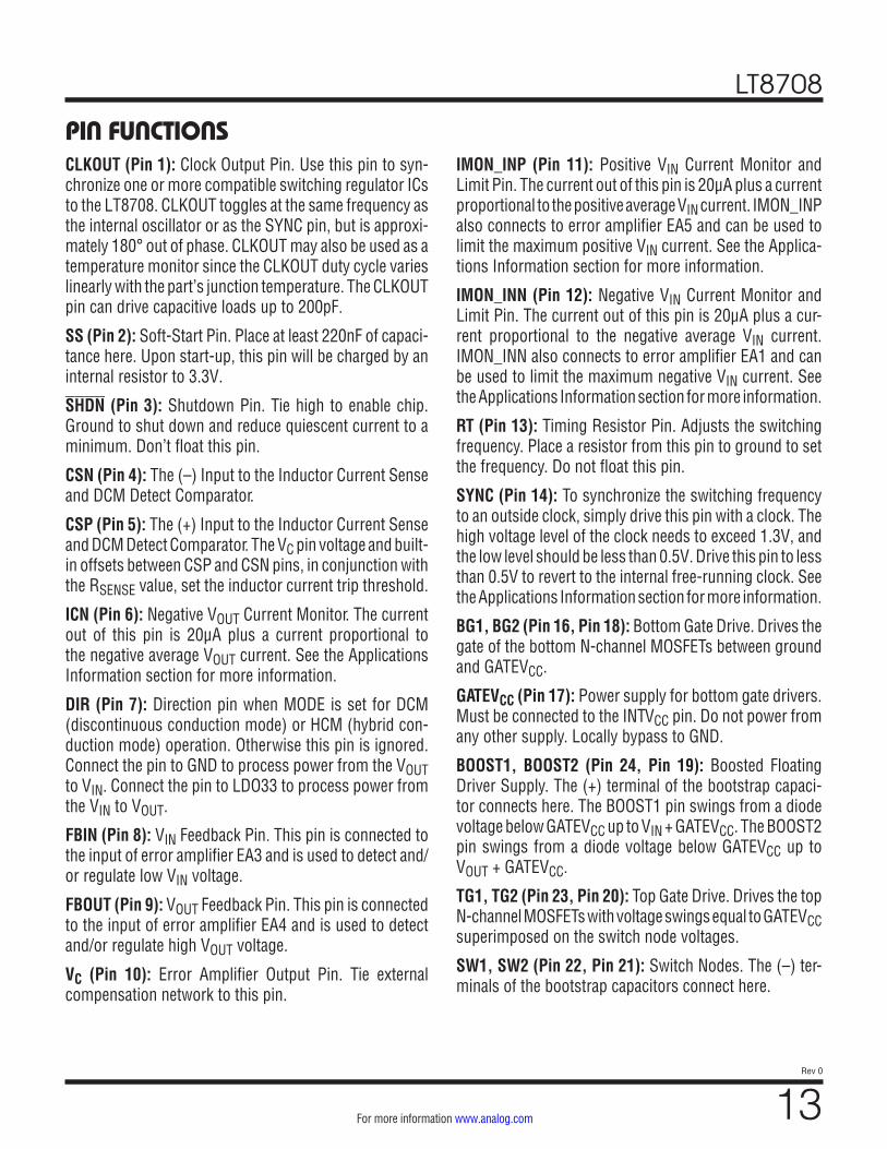
CLKOUT (Pin 1): Clock Output Pin. Use this pin to syn-chronize one or more compatible switching regulator ICs to the LT8708. CLKOUT toggles at the same frequency as the internal oscillator or as the SYNC pin, but is approxi-mately 180° out of phase. CLKOUT may also be used as a temperature monitor since the CLKOUT duty cycle varies linearly with the part’s junction temperature. The CLKOUT pin can drive capacitive loads up to 200pF.
SS (Pin 2): Soft-Start Pin. Place at least 220nF of capaci-tance here. Upon start-up, this pin will be charged by an internal resistor to 3.3V.
SHDN (Pin 3): Shutdown Pin. Tie high to enable chip. Ground to shut down and reduce quiescent current to a minimum. Don’t float this pin.
CSN (Pin 4): The (–) Input to the Inductor Current Sense and DCM Detect Comparator.
CSP (Pin 5): The (+) Input to the Inductor Current Sense and DCM Detect Comparator. The VC pin voltage and built-in offsets between CSP and CSN pins, in conjunction with the RSENSE value, set the inductor current trip threshold.
ICN (Pin 6): Negative VOUT Current Monitor. The current out of this pin is 20μA plus a current proportional to the negative average VOUT current. See the Applications Information section for more information.
DIR (Pin 7): Direction pin when MODE is set for DCM (discontinuous conduction mode) or HCM (hybrid con-duction mode) operation. Otherwise this pin is ignored. Connect the pin to GND to process power from the VOUT to VIN. Connect the pin to LDO33 to process power from the VIN to VOUT.
FBIN (Pin 8): VIN Feedback Pin. This pin is connected to the input of error amplifier EA3 and is used to detect and/or regulate low VIN voltage.
FBOUT (Pin 9): VOUT Feedback Pin. This pin is connected to the input of error amplifier EA4 and is used to detect and/or regulate high VOUT voltage.
VC (Pin 10): Error Amplifier Output Pin. Tie external compensation network to this pin.
IMON_INP (Pin 11): Positive VIN Current Monitor and Limit Pin. The current out of this pin is 20μA plus a current proportional to the positive average VIN current. IMON_INP also connects to error amplifier EA5 and can be used to limit the maximum positive VIN current. See the Applica-tions Information section for more information.
IMON_INN (Pin 12): Negative VIN Current Monitor and Limit Pin. The current out of this pin is 20μA plus a cur-rent proportional to the negative average VIN current. IMON_INN also connects to error amplifier EA1 and can be used to limit the maximum negative VIN current. See the Applications Information section for more information.
RT (Pin 13): Timing Resistor Pin. Adjusts the switching frequency. Place a resistor from this pin to ground to set the frequency. Do not float this pin.
SYNC (Pin 14): To synchronize the switching frequency to an outside clock, simply drive this pin with a clock. The high voltage level of the clock needs to exceed 1.3V, and the low level should be less than 0.5V. Drive this pin to less than 0.5V to revert to the internal free-running clock. See the Applications Information section for more information.
BG1, BG2 (Pin 16, Pin 18): Bottom Gate Drive. Drives the gate of the bottom N-channel MOSFETs between ground and GATEVCC.
GATEVCC (Pin 17): Power supply for bottom gate drivers. Must be connected to the INTVCC pin. Do not power from any other supply. Locally bypass to GND.
BOOST1, BOOST2 (Pin 24, Pin 19): Boosted Floating Driver Supply. The (+) terminal of the bootstrap capaci-tor connects here. The BOOST1 pin swings from a diode voltage below GATEVCC up to VIN + GATEVCC. The BOOST2 pin swings from a diode voltage below GATEVCC up to VOUT + GATEVCC.
TG1, TG2 (Pin 23, Pin 20): Top Gate Drive. Drives the top N-channel MOSFETs with voltage swings equal to GATEVCC superimposed on the switch node voltages.
SW1, SW2 (Pin 22, Pin 21): Switch Nodes. The (–) ter-minals of the bootstrap capacitors connect here.
PIN FUNCTIONS

LT8708
14Rev 0
For more information www.analog.com
RVSOFF (Pin 25): Reverse Conduction Disable Pin. This is an input/output open-drain pin that requires a pull up resistor. Pulling this pin low disables reverse current op-eration. See the Uni and Bidirectional Conduction section for more information.
VOUTLOMON (Pin 26): VOUT Low Voltage Monitor Pin. Connect a ±1% resistor divider between VOUT, VOUT-LOMON and GND to set an undervoltage level on VOUT. When VOUT is lower than this level, reverse conduction is disabled to prevent drawing current from VOUT. See the Applications Information section for more information.
VINHIMON (Pin 27): VIN High Voltage Monitor Pin. Con-nect a ±1% resistor divider between VIN, VINHIMON and GND in order to set an overvoltage level on VIN. When VIN is higher than this level, reverse conduction is disabled to prevent current flow into VIN. See the Applications Information section for more information.
ICP (Pin 28): Positive VOUT Current Monitor Pin. The cur-rent out of this pin is 20μA plus a current proportional to the positive average VOUT current. See the Applications Information section for more information.
EXTVCC (Pin 29): External VCC Input. When EXTVCC ex-ceeds 6.4V (typical), INTVCC will be powered from this pin. When EXTVCC is lower than 6.4V, the INTVCC will be powered from VINCHIP.
CSPOUT (Pin 30): The (+) Input to the VOUT Current Moni-tor Amplifier. This pin and the CSNOUT pin measure the voltage across the sense resistor, RSENSE2, to provide the VOUT current signals. Connect this pin to VOUT when not in use. See Applications Information section for proper use of this pin.
CSNOUT (Pin 31): The (–) Input to the VOUT Current Monitor Amplifier. Connect this pin to VOUT when not in use. See Applications Information section for proper use of this pin.
CSNIN (Pin 32): The (–) Input to the VIN Current Monitor Amplifier. This pin and the CSPIN pin measure the voltage across the sense resistor, RSENSE1, to provide the VIN cur-rent signals. Connect this pin to VIN when not in use. See Applications Information section for proper use of this pin.
CSPIN (Pin 33): The (+) Input to the VIN Current Monitor Amplifier. Connect this pin to VIN when not in use. See Applications Information section for proper use of this pin.
VINCHIP (Pin 34): Main Input Supply Pin for the LT8708. It must be locally bypassed to ground.
INTVCC (Pin 35): 6.3V Regulator Output. Must be connected to the GATEVCC pin. INTVCC is powered from EXTVCC when the EXTVCC voltage is higher than 6.4V, otherwise INTVCC is powered from VINCHIP. Bypass this pin to ground with a minimum 4.7μF ceramic capacitor.
SWEN (Pin 36): Switching Regulator Enable Pin. Tie high through a resistor to enable the switching. Ground to dis-able switching. This pin is pulled down during shutdown, a thermal lockout or when an internal UVLO (undervoltage lockout) is detected. Don’t float this pin. See the Start-Up: SWEN Pin section for more details.
MODE (Pin 37): Conduction Mode Select Pin. The voltage applied to this pin sets the conduction mode of the control-ler. Apply less than 0.4V to enable continuous conduction mode (CCM). Apply 0.8V to 1.2V to enable the hybrid conduction mode (HCM). Apply 1.6V to 2.0V to enable the discontinuous conduction mode (DCM). Apply more than 2.4V to enable Burst Mode operation.
IMON_OP (Pin 38): Positive VOUT Current Monitor and Limit Pin. The current out of this pin is 20μA plus a cur-rent proportional to the positive average VOUT current. IMON_OP also connects to error amplifier EA6 and can be used to limit the maximum positive VOUT current. See the Applications Information section for more information.
IMON_ON (Pin 39): Negative VOUT Current Monitor and Limit Pin. The current out of this pin is 20μA plus a cur-rent proportional to the negative average VOUT current. IMON_ON also connects to error amplifier EA2 and can be used to limit the maximum negative VOUT current. See the Applications Information section for more information.
LDO33 (Pin 40): 3.3V Regulator Output. Bypass this pin to ground with a minimum 0.1μF ceramic capacitor.
GND (Pin 15, Exposed Pad Pin 41): Ground. Tie directly to local ground plane.
PIN FUNCTIONS

LT8708
15Rev 0
For more information www.analog.com
BLOCK DIAGRAM
Figure 1. Block Diagram
–
+A5
–
+A4
–
+A3–
+
OSC
–
+A2
START-UP LOGIC
UV_VINUV_LDO33 UV_GATEVCC
UV_INTVCC OT
3.3VLDOREG
LDOREG
INTERNALSUPPLY2
INTERNALSUPPLY1
LDO33
EN6.3VLDOREG
–
+
–
+
SS
RSENSE1
VIN
LDO33
LDO33
–
+
6.3VLDOREG
VIN
EXTVCC
INTVCC
EN
1.234V
6.4V
RSHDN2
SHDNRSHDN1
3.3V
RSENSE
CSN CSP SWEN
VINCHIP
CSNIN
CSPIN
IMON_INN
MODE
CLKOUT
SYNC
RT
IMON_INP
RVSDIR
RVS
VC
–
+EA5
–
+
EA6
–
+EA4
–
+EA3
1.209V
IMON_INP
–
+
EA1
–
+EA2
1.21V
IMON_INN1.207V
1.205V
1.207V
–
+A6
A1–+
–
+
1.207V
–
+
EA7
BOOST CAPACITORCHARGE CONTROL
CONTROLAND
STATELOGIC
BOOST1
TG1
SW1
GATEVCC
BG1
GND
BG2
SW2
TG2
BOOST2
RFBIN1
RFBOUT1
RFBOUT2
RFBIN2
FBIN
FBOUT
VIN
RSENSE2
VOUT
RLOMON1
RLOMON2
IMON_ON
ICP
ICN
RLOMON3
RHIMON3
RHIMON2
RHIMON1
IMON_OP
VOUTLOMON
VINHIMON
RVSOFF RRVSOFF
CSNOUT
CSPOUT
CB2
DB2
M3
VINLDO33
M4
M2
D3(OPT)
D4(OPT)
CB1M1
D2(OPT)
D1(OPT)
DB1
8708 F01

LT8708
16Rev 0
For more information www.analog.com
OPERATIONTYPOGRAPHICAL CONVENTIONS
The LT8708 is a high performance 4-switch buck-boost controller that includes features to facilitate bidirectional current and power flow. Using the LT8708, an application can command power to be delivered from VIN to VOUT or from VOUT to VIN as needed. Some terms, listed below, are used throughout this data sheet in reference to the direction of current and power flow. In order to clarify these direction-based concepts, these terms are defined as follows:
VIN and IIN: The VIN side of circuits drawn in this data sheet will always be on the left. VIN is con-nected to the SW1 side of the buck-boost inductor through M1. IIN is the VIN current.
VOUT and IOUT:
The VOUT side of circuits drawn in this data sheet will always be on the right. VOUT is connected to the SW2 side of the buck-boost inductor through M4. IOUT is the VOUT current.
Supply (Input):
Power Source. The power source is most commonly applied to VIN. However, VOUT can be a Supply (or Input) when power is being delivered from VOUT to VIN.
Load (Output):
Devices that are consuming the power. The Load is most commonly connected to VOUT. However, VIN can connect to the Load (or Output) when power is being delivered from VOUT to VIN.
Forward Conduction:
Current or power flowing from the VIN or SW1 node (or side) to the VOUT or SW2 node (or side) of the circuit. This is generally left to right on schematics.
Reverse Conduction:
Current or power flowing from the VOUT or SW2 node (or side) to the VIN or SW1 node (or side) of the circuit. This is general right to left on schematics.
Positive Current:
Current that flows from the SW1 side of the buck-boost inductor to the SW2 side. Also refers to current that flows from VIN and/or into VOUT.
Reverse Current:
Current that flows from the SW2 side of the buck-boost inductor to the SW1 side. Also refers to current that flows from VOUT and/or into VIN.
Refer to the Block Diagram (Figure 1) when reading the following sections about the operation of the LT8708.
START-UP
Figure 2 illustrates the start-up sequence for the LT8708.
Start-Up: SHDN Pin
The master shutdown pin for the chip is SHDN. When driven below 0.35V (LT8708E, LT8708I) or 0.3V (LT8708H), the chip is disabled (CHIP OFF state) and quiescent current is minimal. Increasing the SHDN voltage can increase qui-escent current but will not enable the chip until SHDN is driven above 1.221V (typical) after which the INTVCC and LDO33 regulators are enabled (SWITCHER OFF 1 state). External devices powered by LDO33 can become active at this time if enough voltage is available on VINCHIP or EXTVCC to raise INTVCC, and thus LDO33, to an adequate voltage.
Start-Up: SWEN Pin
The SWEN pin is used to enable the switching regulator after the chip has also been enabled by driving SHDN high. SWEN must be pulled high through a resistor to enable the switching regulator. The typical activation threshold is 1.208V as shown in the Electrical Characteristics section. When the SWEN pin voltage is below the activation thresh-old, the CSP-CSN, CSPIN-CSNIN and CSPOUT-CSNOUT current sense circuits on the chip are disabled.
SWEN has an internal pull-down that is activated when the switching regulator is unable to operate (see CHIP OFF and SWITCHER OFF 1 states in Figure 2). After the chip is able to operate and SWEN is internally pulled down below 0.8V (typical), the internal SWEN pull-down is disabled and start-up can proceed past the SWITCHER OFF1 state.
LDO33 or INTVCC are convenient nodes to pull SWEN up to. Choose a pull-up resistor value that limits the current to less than 200μA when SWEN is pulled low. The SWEN pin can also be digitally driven through a current limiting resistor. Note in the Electrical Characteristics section, the SWEN output low voltage is 0.9V (typical) when SHDN is low and/or VINCHIP is unpowered. The SWEN output low is 0.2V when SHDN is 3V and VINCHIP is powered.

LT8708
17Rev 0
For more information www.analog.com
Figure 2. Start-Up Sequence (All Values are Typical)
OPERATION
SOFT-START
• SS CHARGES UP• WHEN SS > 0.2V ... • SWITCHER ENABLED • VC SOFT-START • M1, M4 ON-TIME SOFT-START
SWITCHER OFF 2
• SWITCHER DISABLED• INTVCC AND LDO33 OUTPUTS ENABLED• SS PULLED LOW
NORMAL MODE
• NORMAL OPERATION
INITIALIZE
SS < 50mV
SS > 1.8V
• SS PULLED LOW• VC FORCED TO COMMAND NEAR ZERO CURRENT LIMIT
(INTVCC AND GATEVCC > 4.81V) ANDLDO33 > 3.075V AND SWEN > 1.208V
TJUNCTION < 160°C AND SHDN > 1.221V AND VINCHIP > 2.5V AND((INTVCC AND GATEVCC < 4.65V)
OR LDO33 < 3.04V)
SWITCHER OFF 1
• SWITCHER DISABLED• INTVCC AND LDO33 OUTPUTS ENABLED• SWEN AND SS PULLED LOW
CHIP OFF
SHDN < 1.181V ORVINCHIP < 2.5V ORTJUNCTION > 165°C
• SWITCHER OFF• LDOs OFF• SWEN PULLED LOW
(INTVCC AND GATEVCC > 4.81V) ANDLDO33 > 3.075V AND SWEN < 0.8V
8708 F02
Start-Up: Soft-Start of Switching Regulator
In the INITIALIZE state, the SS (soft-start) pin is pulled low to prepare for soft-starting the switching regulator. After SS has been discharged to less than 50mV, the SOFT-START state begins. In this state, as SS gradually rises, the soft-start circuitry provides a gradual ramp of VC and the inductor current in the appropriate direction (refer to the VC vs SS Voltage graph in the Typical Per-formance Characteristics section). This prevents abrupt surges of inductor current and helps the output voltage ramp smoothly into regulation. See the Switch Control: Soft-Start section for information about the power switch control during soft-start.
During soft-start, an integrated 180k (typical) resistor pulls SS up to 3.3V. The rising ramp rate of the SS pin voltage is set by this 180k resistor and the external capacitor
connected to this pin. When SS reaches 1.8V (typical), the LT8708 exits soft-start and enters normal operation. Typical values for the external soft-start capacitor range from 220nF to 2μF. A minimum of 220nF is recommended.
CONTROL OVERVIEW
The LT8708 is a current mode controller that provides an output voltage above, below or equal to the input volt-age. It also provides bidirectional current monitoring and regulation capabilities at both the input and the output.
The ADI proprietary control architecture employs an inductor current-sensing resistor (RSENSE) in buck, boost or buck-boost regions of operation. The inductor current is controlled by the voltage on the VC pin, which is the combined output of six internal error amplifiers EA1 – EA6. These amplifiers

LT8708
18Rev 0
For more information www.analog.com
with constant current (EA6) to a maximum voltage (EA4) and also reversed, at times, to supply power back to VIN using the other error amplifiers to regulate VIN and limit the maximum current.
POWER SWITCH CONTROL
The following discussions about the power switch control assume that the LT8708 is operating in the continuous conduction mode (see Bidirectional Conduction: CCM). Other conduction modes have slight differences that are discussed later in their respective Conduction sections.
Figure 3 shows a simplified diagram of how the four power switches are connected to the inductor, VIN, VOUT and ground. Figure 4 shows the regions of operation for the LT8708 as a function of VOUT – VIN or switch duty cycle (DC). The power switches are properly controlled so the transfer between modes is continuous.
OPERATION
Figure 3. Simplified Diagram of the Buck-Boost Switches
Figure 4. Operating Regions vs VOUT − VIN
TG1
BG1
TG2
BG2
RSENSE
8708 F03
M1
M2
M4
M3
LSW1 SW2
VIN VOUT
M1 ON, M2 OFFPWM M3, M4 SWITCHES
M4 ON, M3 OFFPWM M1, M2 SWITCHES
4-SWITCH PWM
V OUT
-VIN
SWITCHM3 DCMAX
SWITCHM2 DCMAX
SWITCHM3 DCMINSWITCHM2 DCMIN
BOOST REGION
BUCK REGION
0 BUCK/BOOST REGION
8708 F04
can be used to limit or regulate their respective voltages or currents as shown in Table 1.
Table 1. Error Amplifiers (EA1 − EA6)AMPLIFIER NAME PIN NAME USED TO LIMIT OR REGULATE
EA1 IMON_INN Negative IINEA2 IMON_ON Negative IOUT
EA3 FBIN VIN Voltage
EA4 FBOUT VOUT Voltage
EA5 IMON_INP Positive IINEA6 IMON_OP Positive IOUT
The VC voltage typically has a min-max range of about 1.2V. The maximum VC voltage commands the most positive inductor current and, thus, commands the most power flow from VIN to VOUT. The minimum VC voltage commands the most negative inductor current and, thus, commands the most power flow from VOUT to VIN.
In a simple example of VOUT regulation, the FBOUT pin receives the VOUT voltage feedback signal which is com-pared to the internal reference voltage using EA4. Low VOUT voltage raises VC and, thus, more current flows into VOUT. Conversely, higher VOUT reduces VC, thus, reducing the current into VOUT or even drawing current and power from VOUT.
Note that the current and power flow can also be restricted to one direction, as needed, by the selected conduction mode discussed in the Uni and Bidirectional Conduction section.
As mentioned previously, the LT8708 also provides bidirectional current regulation capabilities at both the input and the output. The VOUT current can be regulated or limited in the forward and reverse directions (EA6 and EA2, respectively). The VIN current can also be regulated or limited in the forward direction and reverse directions (EA5 and EA1, respectively).
In a common application, VOUT might be regulated using EA4, while the remaining error amplifiers are monitoring for excessive input or output current or an input undervoltage condition. In other applications, such as a battery backup system, a battery connected to VOUT might be charged

LT8708
19Rev 0
For more information www.analog.com
Switch Control: Buck Region (VIN >> VOUT)
When VIN is significantly higher than VOUT, the part will run in the buck region. In this region M3 is always off and switch M4 is always on. At the start of every cycle, synchronous switch M2 is turned on first. Inductor current is sensed by amplifier A4 while switch M2 is on. A slope compensation ramp is added to the sensed voltage which is then compared by A5 to a reference that is proportional to VC. After the sensed inductor current falls below the reference, switch M2 is turned off and switch M1 is turned on for the remainder of the cycle. Switches M1 and M2 will alternate, behaving like a typical synchronous buck regulator. Figure 5 shows the switching waveforms in the buck region.
When VIN is much higher than VOUT, the duty cycle of switch M2 will increase, causing the M2 switch off-time to decrease. The M2 switch off-time should be kept above 230ns (typical, see Electrical Characteristics) to maintain steady-state operation and avoid duty cycle jitter, increased output ripple and reduction in maximum output current.
Switch Control: Buck-Boost (VIN ≅ VOUT)
When VIN is close to VOUT, the controller operates in the buck-boost region. Figure 6 shows typical waveforms in this region. Every cycle, if the controller starts with switches M2 and M4 turned on, the controller first oper-ates as if in the buck region. When A5 trips, switch M2 is turned off and M1 is turned on until the middle of the clock cycle. Next, switch M4 turns off and M3 turns on. The LT8708 then operates as if in boost mode until A2 trips. Finally, switch M3 turns off and M4 turns on until the end of the cycle.
If the controller starts with switches M1 and M3 turned on, the controller first operates as if in the boost region. When A2 trips, switch M3 is turned off and M4 is turned on until the middle of the clock cycle. Next, switch M1
Figure 5. Buck Region (VIN >> VOUT)
OPERATION
SWITCH M1
CLOCK
SWITCH M2
SWITCH M3
SWITCH M4
IL
OFF
ON
8708 F05
The part will continue operating in the buck region over a range of switch M2 duty cycles. The duty cycle of switch M2 in the buck region is given by:
DC(M2,BUCK) = 1–
VOUTVIN
⎛
⎝
⎜⎜⎜
⎞
⎠
⎟⎟⎟ •100%
As VIN and VOUT get closer to each other, the duty cycle decreases until the minimum duty cycle of the converter, in the buck region, reaches DC(ABSMIN,M2,BUCK). If the duty cycle becomes lower than DC(ABSMIN,M2,BUCK) the part will move to the buck-boost region.
DC(ABSMIN,M2,BUCK) ≅ tON(M2,MIN) • ƒ •100%
where:
tON(M2,MIN) is the minimum on-time for the synchro-nous switch in buck operation (200ns typical, see Electrical Characteristics).
ƒ is the switching frequency. Figure 6. Buck-Boost Region
SWITCH M1
CLOCK
SWITCH M2
SWITCH M3
SWITCH M4
IL8708 F06a
6(a) Buck-Boost Region (VIN ≥ VOUT)
SWITCH M1
CLOCK
SWITCH M2
SWITCH M3
SWITCH M4
IL
8708 F06b
6(a) Buck-Boost Region (VIN ≤ VOUT)

LT8708
20Rev 0
For more information www.analog.com
turns off and M2 turns on. The LT8708 then operates as if in buck mode until A5 trips. Finally, switch M2 turns off and M1 turns on until the end of the cycle.
Switch Control: Boost Region (VIN << VOUT)
When VOUT is significantly higher than VIN, the part oper-ates in the boost region. In this region switch M1 is always on and switch M2 is always off. At the start of every cycle, switch M3 is turned on first. Inductor current is sensed by amplifier A4 while switch M3 is on. A slope compensation ramp is added to the sensed voltage which is then compared (A2) to a reference that is proportional to VC. After the sensed inductor current rises above the reference voltage, switch M3 is turned off and switch M4 is turned on for the remainder of the cycle. Switches M3 and M4 will alternate, behaving like a typical synchronous boost regulator.
The part will continue operating in the boost region over a range of switch M3 duty cycles. The duty cycle of switch M3 in the boost region is given by:
DC(M3,BOOST) = 1–
VINVOUT
⎛
⎝
⎜⎜⎜
⎞
⎠
⎟⎟⎟ •100%
As VIN and VOUT get closer to each other, the duty cycle decreases until the minimum duty cycle of the converter, in the boost region, reaches DC(ABSMIN,M3,BOOST). If the duty cycle becomes lower than DC(ABSMIN,M3,BOOST), the part will move to the buck-boost region.
DC(ABSMIN,M3,BOOST) ≅ tON(M3,MIN) • ƒ •100%
where:
tON(M3,MIN) is the minimum on-time for the main switch in boost operation (200ns typical, see Electrical Characteristics).
ƒ is the switching frequency.
When VOUT is much higher than VIN, the duty cycle of switch M3 will increase, causing the M3 switch off-time to decrease. The M3 switch off-time should be kept above 230ns (typical, see Electrical Characteristics) to maintain steady-state operation and avoid duty cycle jitter, increased output ripple and reduction in maximum output current.
Figure 7. Boost Region (VIN << VOUT)
Switch Control: Soft-Start
During soft-start, the LT8708 operates in the same three regions discussed above (buck, buck-boost and boost). However, a few differences in switch control happen dur-ing soft-start.
First, M1 and M4 are not turned on simultaneously while SS ramps up to 0.8V (typical). When M1 and M4 would normally both be on, they are instead turned off, leaving all four switches off. After SS rises above 0.8V, during the time when M1 and M4 would normally both be on, they are turned on briefly instead. This brief amount of time increases as SS rises until M1 & M4 are allowed to remain on as long as the normal switching sequence requires.
Second, M2 and M3 will occasionally turn on together for one cycle to refresh both boost capacitors. This refresh cycle happens because M1 and M4 switch more frequently during soft-start than in normal operation. As such, the Boost Capacitor Charge Control block (see Figure 1) can-not always keep the boost capacitors charged. M2 and M3 are turned on when either BOOSTx-SWx voltage drops below 5V (typical). Note that during the refresh cycle, the inductor current slope is nearly zero, thus the boost capacitors can be refreshed without much disturbance to the ongoing switching operations.
UNI AND BIDIRECTIONAL CONDUCTION
The LT8708 has one bidirectional and three unidirectional current conduction modes, primarily selected by the MODE pin. The bidirectional mode (CCM: continuous conduction mode) allows current and power to flow from VIN to VOUT, or vice versa, under control of the VC pin. The unidirectional
OPERATION
SWITCH M1
CLOCK
SWITCH M2
SWITCH M3
SWITCH M4
IL
OFF
ON
8708 F07
LT8708
21Rev 0
For more information www.analog.com
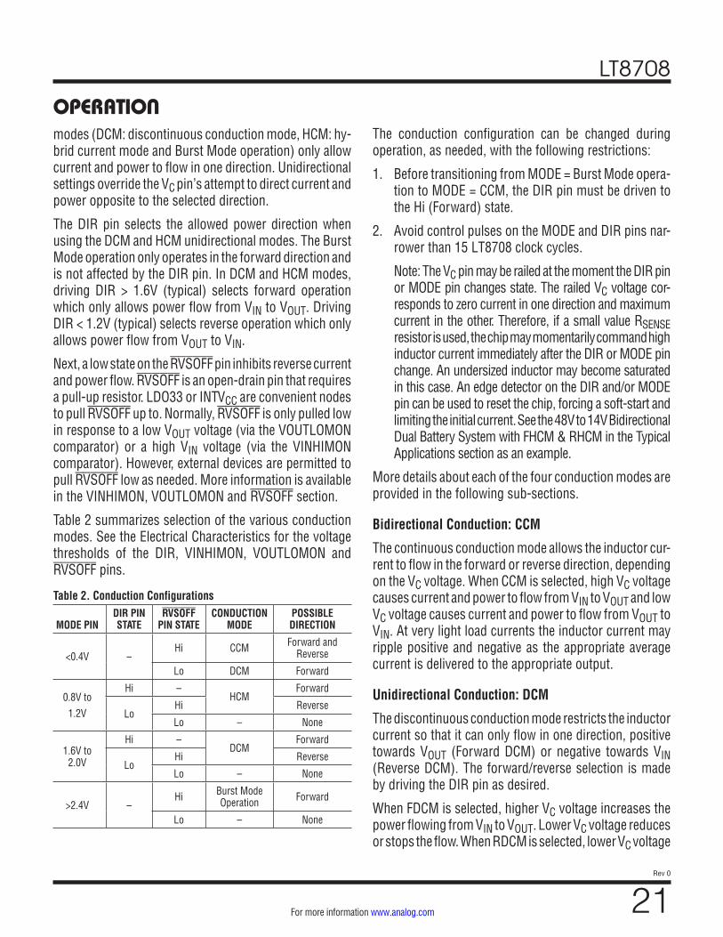
modes (DCM: discontinuous conduction mode, HCM: hy-brid current mode and Burst Mode operation) only allow current and power to flow in one direction. Unidirectional settings override the VC pin’s attempt to direct current and power opposite to the selected direction.
The DIR pin selects the allowed power direction when using the DCM and HCM unidirectional modes. The Burst Mode operation only operates in the forward direction and is not affected by the DIR pin. In DCM and HCM modes, driving DIR > 1.6V (typical) selects forward operation which only allows power flow from VIN to VOUT. Driving DIR < 1.2V (typical) selects reverse operation which only allows power flow from VOUT to VIN.
Next, a low state on the RVSOFF pin inhibits reverse current and power flow. RVSOFF is an open-drain pin that requires a pull-up resistor. LDO33 or INTVCC are convenient nodes to pull RVSOFF up to. Normally, RVSOFF is only pulled low in response to a low VOUT voltage (via the VOUTLOMON comparator) or a high VIN voltage (via the VINHIMON comparator). However, external devices are permitted to pull RVSOFF low as needed. More information is available in the VINHIMON, VOUTLOMON and RVSOFF section.
Table 2 summarizes selection of the various conduction modes. See the Electrical Characteristics for the voltage thresholds of the DIR, VINHIMON, VOUTLOMON and RVSOFF pins.
Table 2. Conduction Configurations
MODE PINDIR PIN STATE
RVSOFF PIN STATE
CONDUCTION MODE
POSSIBLE DIRECTION
<0.4V –Hi CCM Forward and
Reverse
Lo DCM Forward
0.8V to1.2V
Hi –HCM
Forward
LoHi Reverse
Lo – None
1.6V to 2.0V
Hi –DCM
Forward
LoHi Reverse
Lo – None
>2.4V –Hi Burst Mode
Operation Forward
Lo – None
The conduction configuration can be changed during operation, as needed, with the following restrictions:
1. Before transitioning from MODE = Burst Mode opera-tion to MODE = CCM, the DIR pin must be driven to the Hi (Forward) state.
2. Avoid control pulses on the MODE and DIR pins nar-rower than 15 LT8708 clock cycles.
Note: The VC pin may be railed at the moment the DIR pin or MODE pin changes state. The railed VC voltage cor-responds to zero current in one direction and maximum current in the other. Therefore, if a small value RSENSE resistor is used, the chip may momentarily command high inductor current immediately after the DIR or MODE pin change. An undersized inductor may become saturated in this case. An edge detector on the DIR and/or MODE pin can be used to reset the chip, forcing a soft-start and limiting the initial current. See the 48V to 14V Bidirectional Dual Battery System with FHCM & RHCM in the Typical Applications section as an example.
More details about each of the four conduction modes are provided in the following sub-sections.
Bidirectional Conduction: CCM
The continuous conduction mode allows the inductor cur-rent to flow in the forward or reverse direction, depending on the VC voltage. When CCM is selected, high VC voltage causes current and power to flow from VIN to VOUT and low VC voltage causes current and power to flow from VOUT to VIN. At very light load currents the inductor current may ripple positive and negative as the appropriate average current is delivered to the appropriate output.
Unidirectional Conduction: DCM
The discontinuous conduction mode restricts the inductor current so that it can only flow in one direction, positive towards VOUT (Forward DCM) or negative towards VIN (Reverse DCM). The forward/reverse selection is made by driving the DIR pin as desired.
When FDCM is selected, higher VC voltage increases the power flowing from VIN to VOUT. Lower VC voltage reduces or stops the flow. When RDCM is selected, lower VC voltage
OPERATION

LT8708
22Rev 0
For more information www.analog.com
increases the power flowing from VOUT into VIN. Higher VC voltage reduces or stops the flow.
Forward (or reverse) DCM affects the power switches as follows. Under light loading conditions, in FDCM (or RDCM), synchronous switch M4 (or M1) is turned off whenever instantaneous reverse (or forward) current in the inductor is detected. This is to prevent drawing current from VOUT (or VIN) and feeding current into VIN (or VOUT). Under very light loads, the current comparator may also remain tripped for several cycles and force switches M1 (or M2) and M3 (or M4) to stay off for the same number of cycles i.e., skipping pulses. Synchronous switch M2 (or M3) will remain on during the skipped cycles, but since switch M4 (or M1) is off, the inductor current will not reverse directions.
Unidirectional Conduction: HCM
Large inductor current ripple can sometimes result in high power dissipation of the M4 (or M1) junction diode during the FDCM (or RDCM) operation described above. This can happen, for example, when VIN >> VOUT and the average VOUT current is relatively high, but M4 is turned off to block negative components of the AC inductor cur-rent. The hybrid current mode (or HCM) is an alternative to DCM that often reduces the maximum M4 (or M1) heating in such cases.
The hybrid current mode is a mixture of the light load DCM operation and CCM operation, but only allows aver-age current flow in one direction. As such, it is possible to have the lower portions of the inductor current ripple flow opposite to the selected direction while the average current remains in the selected direction. The DIR pin is used to select the desired forward (or FHCM) or reverse (or RHCM) direction of average current flow.
HCM works by measuring the average forward VOUT cur-rent and the average reverse VIN current indicated on ICN and IMON_INP, respectively. In FHCM (or RHCM), light load is detected when ICN (or IMON_INP) is above 255mV (typical). As a result, M4 (or M1) is turned off to prevent average current flow opposite to the desired direction. Heavy load is detected when ICN (or IMON_INP) is below 205mV (typical). As a result, CCM operation is enabled,
allowing M4 (or M1) to turn on and reduce the diode’s power dissipation.
NOTE: In FHCM operation connect a 17.4k resistor from ground to the ICN pin, and in RHCM operation, connect a 17.4k resistor from ground to the IMON_INP pin.
Unidirectional Conduction: Burst Mode
In Burst Mode operation, a VC voltage is set, with about 25mV of hysteresis, below which switching activity is inhibited and above which switching activity is re-enabled. A typical example is when, at light output currents, VOUT rises and forces the VC pin below the threshold that tem-porarily inhibits switching. After VOUT drops slightly and VC rises ~25mV, the switching is resumed, initially in the buck-boost region. Burst Mode operation can increase ef-ficiency at light load currents by eliminating unnecessary switching activity and related power losses. In Burst Mode operation, inductor current is only allowed in the forward direction, regardless of the voltage on the DIR pin. Burst Mode operation handles reverse-current detection similar to forward DCM. The M4 switch is turned off when reverse inductor current is detected.
ERROR AMPLIFIERS
The six internal error amplifiers combine to drive VC ac-cording to Table 3, with the highest priority being at the top.
Table 3. Error Amp PrioritiesTYPICAL CONDITION PURPOSE
ifIMON_INN > 1.21V or then VC
Risesto Reduce Negative IIN
IMON_ON > 1.21V to Reduce Negative IOUT
else if
FBIN < 1.205V or
then VC Falls
to Reduce Positive IIN or Increase Negative IIN
FBOUT > 1.207V or to Reduce Positive IOUT or Increase Negative IOUT
IMON_INP > 1.209V or to Reduce Positive IINIMON_OP > 1.209V to Reduce Positive IOUT
else VC Rises Default
Note that certain error amplifiers are disabled under the conditions shown in Table 4. A disabled error amplifier is unable to affect VC and can be treated as if its associated row is removed from Table 3.
OPERATION

LT8708
23Rev 0
For more information www.analog.com
Table 4. Automatically Disabled Error Amp Conditions
ERROR AMP PIN NAME
VOUTLOMON ASSERTED
VINHIMON ASSERTED
RDCM or RHCM
–RVSOFF <1.207V
EA1 IMON_INN 4*
EA2 IMON_ON 4*
EA3 FBIN 2* 4*
EA4 FBOUT 1* 3* 4*
EA5 IMON_INP 4*
EA6 IMON_OP 4*
A 1* – 4* indicates that the error amplifier listed for that row is disabled under that column’s condition. The purposes of disabling the respective amplifiers are listed below.1* This improves transient response when VOUTLOMON deasserts.2* This improves transient response when VINHIMON deasserts.3* Since power can only transfer from VOUT to VIN, this prevents higher FBOUT/VOUT voltages from interfering with the FBIN/VIN voltage regulation.4* No switching occurs in this condition. Disabling the error amplifiers improves transient response when resuming switching operation.
Some applications don’t require the use of all six error amplifiers. When unused, the respective input pin(s) should be driven so that they don’t interfere with the operation of the remaining amplifiers. Use Table 5 as a guide.
Table 5. Disabling Unused AmplifiersAMPLIFIER
NAME PIN NAME TIE TO DISABLEEXAMPLE DISABLED
PIN CONNECTION
EA1 IMON_INN< 0.9V GND
EA2 IMON_ON
EA3 FBIN > 1.5V LDO33
EA4 FBOUT
< 0.9V GNDEA5 IMON_INP
EA6 IMON_OP
VOUT REGULATION AND SENSING
Two pins, FBOUT and VOUTLOMON, are provided to sense the VOUT voltage and issue the appropriate response to the switching regulator.
VOUT: Regulation
VOUT is regulated, subject to the priorities in Table 3, us-ing a resistor divider between VOUT, FBOUT and ground. FBOUT connects to the EA4 amplifier to drive VC. When FBOUT rises near or above the EA4 reference (1.207V typical), VC typically falls, commanding less current into VOUT. The VOUT regulation voltage is given by the equation:
VOUT = 1.207V • 1+
RFBOUT1RFBOUT2
⎛
⎝
⎜⎜⎜
⎞
⎠
⎟⎟⎟
where:
RFBOUT1 and RFBOUT2 are shown in Figure 1.
VOUT: Above Regulation
When the FBOUT pin and EA4 detect that VOUT is signifi-cantly above regulation, VC typically falls to its minimum voltage. The LT8708 responds to the minimum VC voltage according to the conduction mode enabled by MODE, DIR and RVSOFF. If reverse conduction is not allowed (FDCM, FHCM and Burst Mode operation) then switching will stop and current won’t be delivered to VIN. If reverse conduc-tion is allowed (CCM, RDCM and RHCM), then current and power will flow from VOUT to VIN.
VOUT: Below Regulation and Undervoltage
When the FBOUT pin and EA4 detect VOUT is below regula-tion, VC typically rises. If forward conduction is enabled (CCM, FDCM, FHCM and Burst mode), then current and power will flow from VIN to VOUT.
A resistor divider between VOUT, VOUTLOMON and ground is used to detect VOUT undervoltage. This function prevents reverse conduction, from VOUT to VIN, from drawing VOUT down lower than desired. When undervoltage is detected by VOUTLOMON, RVSOFF is pulled low to disable reverse current and power. This function can be used as a UVLO (undervoltage lockout), for example, when a battery or supercapacitor, connected to VOUT, is supplying power to VIN. See the VINHIMON, VOUTLOMON and RVSOFF section for more detailed information.
OPERATION

LT8708
24Rev 0
For more information www.analog.com
VIN REGULATION AND SENSING
Two pins, FBIN and VINHIMON, are provided to sense the VIN voltage and issue the appropriate response to the switching regulator.
VIN: Regulation
Subject to the priorities in Table 3, a resistor divider be-tween VIN, FBIN and ground can be used to regulate VIN or serve an undervoltage lockout function. A few application examples are as follows:
• For VIN supplies with high source impedance (i.e., a solar panel), VIN regulation can prevent the supply voltage from dropping too low under high VOUT load conditions.
• For VIN supplies with low source impedance (i.e., batteries and voltage supplies), the FBIN pin can be used to stop switching activity when the VIN supply voltage gets too low for proper system operation.
• VIN can also be regulated to a maximum voltage when power is flowing from VOUT to VIN, such as in a battery backup application.
When FBIN falls near or below the EA3 reference (1.205V typical), the VC voltage falls and reduces current draw from VIN. The VIN regulation voltage is given by the equation:
VIN = 1.205V • 1+
RFBIN1RFBIN2
⎛
⎝
⎜⎜⎜
⎞
⎠
⎟⎟⎟
where:
RFBIN1 and RFBIN2 are shown in Figure 1.
VIN: Above Regulation and Overvoltage
When the FBIN pin and EA3 detect VIN is above regulation, VC is allowed to rise. If forward conduction is enabled (CCM, FDCM, FHCM and Burst Mode operation), then current and power can flow from VIN to VOUT. If only reverse conduc-tion is enabled (RDCM and RHCM), then switching will stop and current won’t be delivered into VIN. NOTE: This above-regulation condition is required to allow forward conduction in an application.
A resistor divider between VIN, VINHIMON and ground is used to detect VIN overvoltage. This function prevents reverse conduction, from VOUT to VIN, from forcing VIN higher than desired. When overvoltage is detected by VIN-HIMON, RVSOFF is pulled low to disable reverse current and power. This function can be used as an OVLO (over voltage lockout), for example, when a battery, connected to VIN, is being charged from VOUT. See the VINHIMON, VOUTLOMON and RVSOFF section for more detailed information.
VIN: Below Regulation
When the FBIN pin and EA3 detect that VIN is significantly below regulation, VC may fall to its minimum voltage. The LT8708 responds to the minimum VC voltage according to the conduction mode enabled by MODE, DIR and RVSOFF. If only forward conduction is allowed (FDCM, FHCM and Burst Mode operation) then switching will stop and cur-rent won’t be drawn from VOUT. If reverse conduction is allowed (CCM, RDCM and RHCM), then current and power will flow from VOUT to VIN.
UVLO functions are available to detect low VIN voltage. These functions are discussed in the Voltage Lockouts section.
CURRENT MONITORING AND LIMITING
Monitoring and Limiting: IMON Pins
The LT8708 can monitor VIN and VOUT current (IIN and IOUT) in both the positive and negative directions. The CSPIN and CSNIN pins connect across a current sense resistor to monitor IIN. External resistors are connected from the IMON_INP and IMON_INN pins to GND. Their resulting voltages are linearly proportional to positive IIN and negative IIN respectively. See amplifier A3 in the Block Diagram.
Similarly, an IOUT sense resistor, measured by CSPOUT and CSNOUT, is used to monitor the VOUT current. External resistors are connected from the IMON_OP and IMON_ON pins to GND. Their resulting voltages are linearly propor-tional to positive IOUT and negative IOUT respectively. See amplifier A1 in the Block Diagram.
OPERATION

LT8708
25Rev 0
For more information www.analog.com
The IIN and IOUT currents can be limited and regulated to independent maximum positive values. When IIN causes IMON_INP to rise near or above 1.209V (typical), EA5 typically causes VC to pull down and limit/regulate the maximum current. Similarly, when IOUT causes IMON_OP to rise near or above 1.209V (typical), EA6 typically causes VC to pull down and limit/regulate the maximum current. See Table 3 for error amplifier priorities.
The IIN and IOUT currents can also be limited and regu-lated to independent maximum negative values. When IIN causes IMON_INN to rise near or above 1.21V (typical), EA1 causes VC to pull up and limit the maximum current. Similarly, when IOUT causes IMON_ON to rise near or above 1.21V (typical), EA2 causes VC to pull up and limit the maximum current.
The IIN and IOUT current limits can provide many benefits. They can be used to prevent overloading the input sup-ply, allow for constant-current battery and supercapacitor charging and can also serve as short-circuit protection for constant-voltage regulators. See the Applications In-formation section for more information about the current monitors and the current regulation and limiting.
Monitoring: ICP and ICN Pins
ICP and ICN are additional current monitor pins with output currents typically equal to those of IMON_OP and IMON_ON, respectively.
In contrast to IMON_OP, ICP is internally pulled to ~0.6V (typical) when VC is at its minimum and the conduction mode is either RDCM or RHCM. Also, in contrast to IMON_ON, ICN is internally pulled to ~0.6V (typical) when VC is at its maximum and the conduction mode is FDCM, FHCM or Burst Mode operation.
Always connect a 17.4k resistor from ICP to ground and from ICN to ground.
INTVCC/EXTVCC/GATEVCC/LDO33 POWER
Power for the top and bottom MOSFET drivers, the LDO33 pin and most internal circuitry is derived from the INTVCC pin. INTVCC is regulated to 6.3V (typical) from either the VINCHIP or EXTVCC pin. When the EXTVCC pin is left open or tied to a voltage less than 6.2V (typical), an internal low dropout regulator regulates INTVCC from VINCHIP. If EXTVCC is taken above 6.4V (typical), another low dropout regula-tor will instead regulate INTVCC from EXTVCC. Regulating INTVCC from EXTVCC allows the power to be derived from the lowest supply voltage (highest efficiency) such as the LT8708 switching regulator output (see INTVCC Regulators and EXTVCC Connection in the Applications Information section for more details).
The GATEVCC pin directly powers the bottom MOSFET drivers for switches M2 and M3 (see Figure 3). GATEVCC should always be connected to INTVCC and should not be powered or connected to any other source. Undervolt-age lockouts (UVLOs) monitoring INTVCC and GATEVCC disable the switching regulator when the pins are below 4.65V (typical).
The LDO33 pin can provide power to external components such as a microcontroller and/or can provide an accurate bias voltage. Load current is limited to 17.25mA (typical). As long as SHDN is high, the LDO33 output is linearly regulated from the INTVCC pin and is not affected by the INTVCC or GATEVCC UVLOs or the SWEN pin voltage. LDO33 remains regulated as long as SHDN is high and sufficient voltage is available on INTVCC (typically > 4.0V). An undervoltage lockout monitoring LDO33 will disable the switching regulator when LDO33 is below 3.04V (typical).
CLKOUT AND TEMPERATURE SENSING
The CLKOUT pin toggles at the LT8708’s internal clock frequency whether the internal clock is synchronized to an external source or is free-running based on the external RT resistor. The CLKOUT pin can be used to synchronize other devices to the LT8708’s switching frequency. Also, the duty cycle of CLKOUT is proportional to the die temperature and can be used to monitor the die for thermal issues.
OPERATION
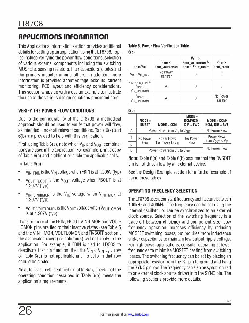
LT8708
26Rev 0
For more information www.analog.com
APPLICATIONS INFORMATIONThis Applications Information section provides additional details for setting up an application using the LT8708. Top-ics include verifying the power flow conditions, selection of various external components including the switching MOSFETs, sensing resistors, filter capacitors, diodes and the primary inductor among others. In addition, more information is provided about voltage lockouts, current monitoring, PCB layout and efficiency considerations. This section wraps up with a design example to illustrate the use of the various design equations presented here.
VERIFY THE POWER FLOW CONDITIONS
Due to the configurability of the LT8708, a methodical approach should be used to verify that power will flow, as intended, under all relevant conditions. Table 6(a) and 6(b) are provided to help with this verification.
First, using Table 6(a), note which VIN and VOUT combina-tions are used in the application. For example, print a copy of Table 6(a) and highlight or circle the applicable cells.
In Table 6(a):
• VIN_FBIN is the VIN voltage when FBIN is at 1.205V (typ)
• VOUT_FBOUT is the VOUT voltage when FBOUT is at 1.207V (typ)
• VIN_VINHIMON is the VIN voltage when VINHIMON at 1.207V (typ)
• VOUT_VOUTLOMON is the VOUT voltage when VOUTLOMON is at 1.207V (typ)
If one or more of the FBIN, FBOUT, VINHIMON and VOUT-LOMON pins are tied to their inactive states (see Table 5 and the VINHIMON, VOUTLOMON and RVSOFF section), the associated row(s) or column(s) will not apply to the application. For example, if FBIN is tied to LDO33 to deactivate that pin function, then the VIN < VIN_FBIN row of Table 6(a) is not applicable and no cells in that row should be circled.
Next, for each cell identified in Table 6(a), check that the operating condition described in Table 6(b) meets the application’s requirements.
Table 6. Power Flow Verification Table6(a)
VOUT/VIN
VOUT < VOUT_VOUTLOMON
VOUT > VOUT_VOUTLOMON & VOUT < VOUT_FBOUT
VOUT > VOUT_FBOUT
VIN < VIN_FBINNo Power Transfer B B
VIN > VIN_FBIN & VIN <
VIN_VINHIMON
A D C
VIN > VIN_VINHIMON
A D No Power Transfer
6(b)
MODE = BURST MODE = CCM
MODE = DCM/HCM, DIR = FWD
MODE = DCM/HCM, DIR = RVS
A Power Flows from VIN to VOUT No Power Flow
B No Power Flow
Power Flows from VOUT to VIN
No Power Flow
Power Flows from VOUT to VIN
CNo Power FlowD Power Flows from VIN to VOUT
Note: Table 6(a) and Table 6(b) assume that the RVSOFF pin is not driven low by an external device.
See the Design Example section for a further example of using these tables.
OPERATING FREQUENCY SELECTION
The LT8708 uses a constant frequency architecture between 100kHz and 400kHz. The frequency can be set using the internal oscillator or can be synchronized to an external clock source. Selection of the switching frequency is a trade-off between efficiency and component size. Low frequency operation increases efficiency by reducing MOSFET switching losses, but requires more inductance and/or capacitance to maintain low output ripple voltage. For high power applications, consider operating at lower frequencies to minimize MOSFET heating from switching losses. The switching frequency can be set by placing an appropriate resistor from the RT pin to ground and tying the SYNC pin low. The frequency can also be synchronized to an external clock source driven into the SYNC pin. The following sections provide more details.

LT8708
27Rev 0
For more information www.analog.com
INTERNAL OSCILLATOR
The operating frequency of the LT8708 can be set using the internal free-running oscillator. When the SYNC pin is driven low (< 0.5V), the operating frequency is set by the value of the resistor from the RT pin to ground. An internally trimmed timing capacitor resides inside the IC. The oscillator frequency is calculated using the following formula:
fOSC =
43,750RT +1
⎛
⎝⎜
⎞
⎠⎟kHz
where:
fOSC is in kHz and RT is in kΩ.
Conversely, RT (in kΩ) can be calculated from the desired frequency (in kHz) using:
RT =
43,750fOSC
– 1⎛
⎝⎜
⎞
⎠⎟kΩ
SYNC PIN AND CLOCK SYNCHRONIZATION
The operating frequency of the LT8708 can be synchronized to an external clock source. To synchronize to the external source, simply provide a digital clock signal into the SYNC pin. The LT8708 will operate at the SYNC clock frequency.
The duty cycle of the SYNC signal must be between 20% and 80% for proper operation. Also, the frequency of the SYNC signal must meet the following two criteria:
1. SYNC may not toggle outside the frequency range of 100kHz to 400kHz unless it is stopped low to enable the free-running oscillator.
2. The SYNC pin frequency can always be higher than the free-running oscillator set frequency, fOSC, but should not be less than 25% below fOSC.
After SYNC begins toggling, it is recommended that switching activity is stopped before the SYNC pin stops toggling. Excess inductor current can result when SYNC stops toggling as the LT8708 transitions from the external SYNC clock source to the internal free-running oscillator clock. Switching activity can be stopped by driving either the SWEN or SHDN pin low.
CLKOUT PIN AND CLOCK SYNCHRONIZATION
The CLKOUT pin can drive up to 200pF and toggles at the LT8708’s internal clock frequency whether the internal clock is synchronized to the SYNC pin or is free-running based on the external RT resistor. The rising edge of CLKOUT is approximately 180° out of phase from the internal clock’s rising edge or the SYNC pin’s rising edge if it is toggling. CLKOUT starts toggling when the INITIALIZE state is entered (see Figure 2).
The CLKOUT pin can be used to synchronize other devices to the LT8708’s switching frequency. For example, the CLKOUT pin can be tied to the SYNC pin of another LT8708 regulator which will operate approximately 180°out of phase of the master LT8708. The frequency of the master LT8708 can be set by the external RT resistor or by toggling the SYNC pin. Note that the RT pin of the slave LT8708 must have a resistor tied to ground. In general, use the same value RT resistor for all of the synchronized LT8708s.
The duty cycle of CLKOUT is proportional to the die tem-perature and can be used to monitor the die for thermal issues. See the Junction Temperature Measurement section for more information.
INDUCTOR CURRENT SENSING AND SLOPE COMPENSATION
The LT8708 operates using inductor current mode control. As described previously in the Power Switch Control sec-tion, the LT8708 measures the peak of the inductor current waveform in the boost region and the valley of the inductor current waveform in the buck region. The inductor current is sensed across the RSENSE resistor with pins CSP and CSN. During any given cycle, the peak (boost region) or valley (buck region) of the inductor current is controlled by the VC pin voltage.
Slope compensation provides stability in constant-frequency current mode control architectures by preventing subhar-monic oscillations at high duty cycles. This is accomplished internally by adding a compensating ramp to the inductor current signal in the boost region, or subtracting a ramp from the inductor current signal in the buck region. At higher duty cycles, this results in a reduction of maximum inductor current in the boost region, and an increase of the maximum
APPLICATIONS INFORMATION

LT8708
28Rev 0
For more information www.analog.com
inductor current in the buck region. For example, refer to the Maximum Inductor Current Sense Voltage vs Duty Cycle graph in the Typical Performance Characteristics section. The graph shows that, with VC at its maximum voltage, the maximum peak inductor sense voltage VRSENSE is between 47mV and 93mV depending on the duty cycle. It also shows that the maximum inductor valley current in the buck region is 82mV increasing to ~130mV at higher duty cycles.
RSENSE SELECTION AND MAXIMUM CURRENT
The RSENSE resistance must be chosen properly to achieve the desired amount of output current (forward conduction) and input current (reverse conduction). Too much resistance can limit the input/output current below the application requirements. Start by determining the maximum allowed RSENSE resistances in the forward and reverse boost regions (RSENSE(MAX,BOOST,FWD) and RSENSE(MAX,BOOST,RVS)). Follow this by finding the maximum allowed RSENSE resistances in the forward and reverse buck regions (RSENSE(MAX,BUCK,FWD) and RSENSE(MAX,BUCK,RVS)). The selected RSENSE resistance must be less than all four values.
RSENSE Selection: Max RSENSE in the Boost Region
Forward Conduction: In this section RSENSE(MAX,BOOST,FWD) is calculated which is the maximum allowed RSENSE re-sistance when operating in the boost region with forward conduction (VIN to VOUT). Skip this section and assume RSENSE(MAX,BOOST,FWD) = ∞ when this operating condition does not apply to the application.
In the boost region, the maximum positive VOUT current capability is the lowest when VIN is at its minimum and VOUT is at its maximum. Therefore, RSENSE must be cho-sen to meet the output current requirements under these conditions.
Start by finding the maximum boost region duty cycle which occurs when VIN is minimum and VOUT is maximum using:
DC(MAX,M3,BOOST) ≅
1–VIN(MIN,BOOST)
VOUT(MAX,BOOST)
⎛
⎝
⎜⎜⎜
⎞
⎠
⎟⎟⎟
•100%
For example, an application with a VIN range of 12V to 48V and VOUT set to 36V will have:
DC(MAX,M3,BOOST) ≅
1–12V36V
⎛
⎝⎜⎜
⎞
⎠⎟⎟ •100% = 67%
Referring to the Maximum Inductor Current Sense Voltage graph in the Typical Performance Characteristics section, the maximum RSENSE voltage at 67% duty cycle is 68mV, or:
VRSENSE(MAX,BOOST,MAXDC) ≅ 68mV
for VIN = 12V, VOUT = 36V.
Next, the inductor ripple current in the boost region must be determined. If the main inductor L is not known, the maximum ripple current ∆IL(MAX,BOOST) can be estimated by choosing ∆IL(MAX,BOOST) to be 30% to 50% of the maxi-mum peak inductor current in the boost region as follows:
∆IL(MAX,BOOST)
VOUT(MAX,BOOST) •IOUT(MAX,FWD)
VIN(MIN,BOOST) • 100%%Ripple
– 0.5A
≅
where:
IOUT(MAX,FWD) is the maximum VOUT load current required in the boost region.
%Ripple is 30% to 50%
For example, using VOUT(MAX) = 36V, VIN(MIN) = 12V, IOUT(MAX,FWD) = 2A and %Ripple = 40% we can calculate:
IL(MAX,BOOST)
36V •2A
12V • 100%40%
– 0.5=3A
≅
APPLICATIONS INFORMATION

LT8708
29Rev 0
For more information www.analog.com
Otherwise, if the inductance is already known then ∆IL(MAX,BOOST,FWD) can be more accurately calculated as follows:
∆IL(MAX,BOOST) =
DC(MAX,M3,BOOST)
100%
⎛
⎝
⎜⎜⎜
⎞
⎠
⎟⎟⎟ • VIN(MIN,BOOST)
ƒ •LA
where:
DC(MAX,M3,BOOST) is the maximum duty cycle percent-age in the boost region as calculated previously
ƒ is the switching frequency
L is the inductance of the main inductor
After the maximum ripple current is known, the maximum allowed RSENSE in the boost region while in forward con-duction (VIN to VOUT) can be calculated as follows:
RSENSE(MAX,BOOST,FWD) =
2 • VRSENSE(MAX,BOOST,MAXDC) • VIN(MIN,BOOST)
2 •IOUT(MAX,FWD) • VOUT(MAX,BOOST)( )+ ∆IL(MAX,BOOST) • VIN(MIN,BOOST)( )Ω
where:
VRSENSE(MAX,BOOST,MAXDC) is the maximum inductor current sense voltage as discussed in the previous section.
Using values from the previous examples:
RSENSE(MAX,BOOST,FWD) =
2 • 68mV •12V2 • 2A • 36V( )+ 3A •12V( )
= 9.1mΩ
Reverse Conduction: In this section RSENSE(MAX,BOOST,RVS) is calculated which is the maximum allowed RSENSE re-sistance when operating in the boost region with reverse conduction (VOUT to VIN). Skip this section and assume RSENSE(MAX,BOOST,RVS) = ∞ when this operating condition does not apply to the application.
In the boost region, the maximum reverse VIN current capability is the lowest when operating at the minimum
duty cycle. See Switch Control: Boost Region (VIN << VOUT) section for the equation to calculate the minimum duty cycle DC(ABSMIN, M3, BOOST).
Before calculating the maximum RSENSE resistance allowed during reverse operation, however, the inductor ripple current must be determined. If the main inductor L is not known, the ripple current ∆IL(MIN,BOOST) can be estimated by choosing ∆IL(MIN,BOOST) to be 10% of the minimum peak inductor current in the boost region as follows:
∆IL(MIN,BOOST)IIN(MAX,RVS)100%10%
– 0.5A≅
where:
IIN(MAX,RVS) is the maximum VIN load current required in the boost region in the reverse direction
If the inductance is already known then ∆IL(MIN,BOOST) can be calculated as follows:
∆IL MIN,BOOST( ) =
DC(ABSMIN,M3,BOOST)
100%
⎛
⎝
⎜⎜⎜
⎞
⎠
⎟⎟⎟ • VIN(MIN,BOOST)
ƒ •LA
where:
DC(ABSMIN,M3,BOOST) is the minimum duty cycle percentage in the boost region (see Switch Control: Boost Region (VIN << VOUT) section)
ƒ is the switching frequency
L is the inductance of the main inductor
Now that the inductor ripple current is known, the maxi-mum allowed RSENSE in the boost region while in reverse conduction can be calculated as follows:
RSENSE(MAX,BOOST,RVS) =
2• | VRSENSE(MIN,BOOST,MINDC) |
2 •IIN(MAX,RVS)( ) – ∆IL(MIN,BOOST)Ω
APPLICATIONS INFORMATION

LT8708
30Rev 0
For more information www.analog.com
where:
VRSENSE(MIN,BOOST,MINDC) is the minimum inductor cur-rent sense voltage in the boost region at the minimum duty cycle. Typical value is –93mV.
Negative result from the above equation indicates that any RSENSE value can meet the requirement. Substitute the calculated result with ∞ and move onto the next section.
RSENSE Selection: Max RSENSE in the Buck Region
Forward Conduction: In this section RSENSE(MAX,BUCK,FWD) is calculated which is the maximum allowed RSENSE re-sistance when operating in the buck region with forward conduction (VIN to VOUT).
In the buck region, the maximum VOUT current capability is the lowest when operating at the minimum duty cycle. See Switch Control: Boost Region (VIN << VOUT) section for the equation to calculate the minimum duty cycle DC(ABSMIN, M2,BUCK).
Before calculating the maximum RSENSE resistance, however, the inductor ripple current must be determined. If the main inductor L is not known, the ripple current ∆IL(MIN,BUCK) can be estimated by choosing ∆IL(MIN,BUCK) to be 10% of the maximum peak inductor current in the buck region as follows:
∆IL(MIN,BUCK)IOUT(MAX,FWD)100%10%
– 0.5A≅
where:
IOUT(MAX,FWD) is the maximum VOUT load current required in the buck region in the forward direction.
If the inductance is already known then ∆IL(MIN,BUCK) can be calculated as follows:
∆IL MIN,BUCK( ) =
DC(ABSMIN,M2,BUCK)
100%
⎛
⎝
⎜⎜⎜
⎞
⎠
⎟⎟⎟ • VOUT(MIN,BUCK)
ƒ •LA
where:
DC(ABSMIN,M2,BUCK) is the minimum duty cycle per-centage in the buck region as calculated previously
ƒ is the switching frequency
L is the inductance of the main inductor
After the inductor ripple current is known, the maximum allowed RSENSE in the buck region while in forward con-duction can be calculated as follows:
RSENSE(MAX,BUCK,FWD) =
2 • VRSENSE(MAX,BUCK,MINDC)
2 •IOUT(MAX,FWD)( ) – ∆IL(MIN,BUCK)Ω
where:
VRSENSE(MAX,BUCK,MINDC) is the maximum inductor current sense voltage at the minimum duty cycle. Typical value is 82mV.
Negative result from the above equation indicates that any RSENSE value can meet the requirement. Substitute the calculated result with ∞ and move onto the next section.
Reverse Conduction: In this section RSENSE(MAX, BUCK, RVS) is calculated which is the maximum allowed RSENSE resistance when operating in the buck region with reverse conduction (VOUT to VIN). Skip this section and assume RSENSE(MAX, BUCK, RVS) = ∞ when this operating condition does not apply to the application.
In the buck region, the maximum reverse VIN current ca-pability is the least when VIN is at its maximum and VOUT is at its minimum for buck operation. Therefore RSENSE must be chosen to meet the VIN current requirements under these conditions.
Start by finding the buck region duty cycle when VIN is minimum and VOUT is maximum using:
DC(MAX,M2,BUCK) ≅
1–VOUT(MIN,BUCK)
VIN(MAX,BUCK)
⎛
⎝
⎜⎜⎜
⎞
⎠
⎟⎟⎟
•100%
APPLICATIONS INFORMATION

LT8708
31Rev 0
For more information www.analog.com
Next, the inductor ripple current in the buck region must be determined. If the main inductor L is not known, the maximum ripple current ∆IL(MAX,BUCK) can be estimated by choosing ∆IL(MAX,BUCK) to be 30% to 50% of the maxi-mum peak inductor current in the buck region as follows:
∆IL(MAX,BUCK)
VIN(MAX,BUCK) •IIN(MAX,RVS)
VOUT(MIN,BUCK) • 100%%Ripple
– 0.5A
≅
where:
IIN(MAX,RVS) is the maximum VIN load current in the reverse direction required in the buck region.
%Ripple is 30% to 50%
Otherwise, if the inductance is already known then ∆IL(MAX,BUCK) can be more accurately calculated as follows:
∆IL(MAX,BUCK) ≅
DC(MAX,M2,BUCK)
100%
⎛
⎝
⎜⎜⎜
⎞
⎠
⎟⎟⎟ • VOUT(MIN,BUCK)
ƒ •LA
where:
DC(MAX,M2,BUCK) is the maximum duty cycle percent-age in the buck region as calculated previously
ƒ is the switching frequency
L is the inductance of the main inductor
After the maximum ripple current is known, the maximum allowed RSENSE in the buck region while in reverse conduc-tion can be calculated as follows:
RSENSE(MAX,BUCK,RVS) =
2• | VRSENSE(MIN,BUCK,MAXDC) | •VOUT(MIN,BUCK)
2• |IIN(MAX,RVS) | •VIN(MAX,BUCK)( )+ ∆IL(MAX,BUCK) • VOUT(MIN,BUCK)( )Ω
APPLICATIONS INFORMATIONwhere:
VRSENSE(MIN,BUCK,MAXDC) is the minimum inductor current sense voltage at the maximum duty cycle. This value is determined in a similar manner to VRSENSE(MAX,BOOST,MAXDC) discussed previously in the RSENSE Selection: Max RSENSE in the Boost Region (Forward Conduction) section.
RSENSE Selection: Final RSENSE Value
The final RSENSE value should be lower than all four maximum RSENSE values, RSENSE(MAX,BOOST,FWD), RSENSE(MAX,BOOST,RVS), RSENSE(MAX,BUCK,FWD) and RSENSE(MAX,BUCK,RVS). A margin of 20% to 30% is rec-ommended.
Figure 8 shows approximately how the maximum posi-tive IOUT and inductor currents would vary with VIN/VOUT while all other operating parameters remain constant (frequency = 120kHz, inductance = 10µH, RSENSE = 1mΩ). This graph is normalized and accounts for changes in maximum current due to the slope compensation ramps and the effects of changing ripple current. The curve is theoretical but can be used as a guide to predict relative changes in maximum currents over a range of VIN/VOUT voltages. Similarly, when in reverse conduction, Figure 9 shows approximately how the maximum negative IIN and inductor currents would vary with VIN/VOUT.
Figure 8. Currents vs VIN/VOUT Ratio in Forward Conduction
VIN/VOUT (V/V)0.1 1 10
0
0.20
0.40
0.60
0.80
1.00
NORM
ALIZ
ED C
URRE
NT
8708 F08
MAXIMUM
OUTPUT
INDUCTORCURRENT
MAXIMUM
CURRENT

LT8708
32Rev 0
For more information www.analog.com
Figure 10. Inductor Current Sense Filter
Figure 9. Currents vs VIN/VOUT Ratio in Reverse Conduction
INDUCTOR (L) SELECTION
For high efficiency, choose an inductor with low core loss, such as ferrite. Also, the inductor should have low DC resistance to reduce the I2R losses, and must be able to handle the peak inductor current without saturating. To minimize radiated noise, use a toroid, pot core or shielded bobbin inductor.
The operating frequency and inductor selection are inter-related in that higher operating frequencies allow the use of smaller inductor and capacitor values. The following sections discuss several criteria to consider when choosing an inductor value. For optimal performance, choose an inductor that meets all of the following criteria.
L Selection: Load Current in Buck and Boost Regions
Small inductances result in increased ripple currents and thus, due to the positive and negative inductor current limits, decrease the maximum average forward IOUT in the boost region and the maximum average reverse IIN in the buck region.
In order to provide adequate forward IOUT at low VIN volt-ages in the boost region, L should be at least:
L(MIN1,BOOST)
VIN(MIN,BOOST) •DC(MAX,M3,BOOST)
100%
2• ƒ •VRSENSE(MAX,BOOST,MAXDC)
RSENSE–
IOUT(MAX,FWD) • VOUT(MAX,BOOST)
VIN(MIN,BOOST)
H
≅
where:
DC(MAX,M3,BOOST) is the maximum duty cycle percent-age of the M3 switch (see RSENSE Selection: Max RSENSE in the Boost Region section)
ƒ is the switching frequency
VRSENSE(MAX,BOOST,MAXDC) is the maximum current sense voltage in the boost region at maximum duty cycle (see RSENSE Selection: Max RSENSE in the Boost Region section)
IOUT(MAX,FWD) is the maximum forward VOUT current in boost region
APPLICATIONS INFORMATION
RSENSE FILTERING
Certain applications may require filtering of the inductor current sense signals due to excessive switching noise that can appear across RSENSE. Higher operating voltages, higher values of RSENSE, and more capacitive MOSFETs will all contribute additional noise across RSENSE when the SW pins transition. The CSP/CSN sense signals can be filtered by adding one of the RC networks shown in Figure 10. Most PC board layouts can be drawn to accommodate either network on the same board. The network should be placed as close as possible to the IC. The network in Figure 10b can reduce common mode noise seen by the CSP/CSN pins of the LT8708 at the expense of some increased ground trace noise as current passes through the capacitors. A short direct path from the capacitor grounds to the IC ground should be used on the PC board. Resistors greater than 10Ω should be avoided as these can increase offset voltages at the CSP/CSN pins. The RC product should be kept to less than 30ns.
VIN/VOUT (V/V)0.1 1 10
0
0.20
0.40
0.60
0.80
1.00
NORM
ALIZ
ED C
URRE
NT
8708 F09
MAXIMUM
INTPUT
INDUCTORCURRENT
MAXIMUM
CURRENT
RSENSE 1nF
CSP
CSN
LT870810Ω
10Ω
RSENSE 1nF
1nF
CSP
CSN
LT8708
8708 F10
10Ω
10Ω
10(a)
10(b)

LT8708
33Rev 0
For more information www.analog.com
To provide adequate reverse IIN current at low VOUT volt-ages in the buck region, L should be at least:L(MIN1,BUCK)
VOUT(MIN,BUCK) •DC(MAX,M2,BUCK)
100%
2• ƒ •|VRSENSE(MIN,BUCK,MAXDC) |
RSENSE–
IIN(MAX,RVS) • VIN(MAX,BUCK)
VOUT(MIN,BUCK)
Ω
≅
where:
DC(MAX,M2,BUCK) is the maximum duty cycle percentage of the M2 switch (see RSENSE Selection: Max RSENSE in the Buck Region section)
ƒ is the switching frequency
VRSENSE(MIN,BUCK,MAXDC) is the minimum current sense voltage in the buck region at maximum duty cycle (see RSENSE Selection: Max RSENSE in the Buck Region section)
IIN(MAX,RVS) is the maximum reverse VIN current in buck region
Negative values of L(MIN1,BOOST) or L(MIN1,BUCK) indicate that the load current can’t be delivered because the induc-tor current limit is too low. If L(MIN1,BOOST) or L(MIN1,BUCK) is too large or is negative, consider reducing the RSENSE resistor value to increase the inductor current limit.
L Selection: Subharmonic Oscillations
The LT8708’s internal slope compensation circuits will prevent subharmonic oscillations that can otherwise occur when VIN/VOUT is less than 0.5 or greater than 2. The slope compensation circuits will prevent these oscil-lations provided that the inductance exceeds a minimum value (see the earlier section Inductor Current Sensing and Slope Compensation for more information). Choose an inductance greater than all of the relevant L(MIN) lim-its discussed below. Negative calculation results can be interpreted as zero.
In the boost region, if VOUT can be greater than twice VIN, calculate L(MIN2,BOOST) as follows:
L(MIN2,BOOST) =
VOUT(MAX,BOOST) –VIN(MIN,BOOST) • VOUT(MAX,BOOST)
VOUT(MAX,BOOST) – VIN(MIN,BOOST)•RSENSE
0.08 • fH
In the buck region, if VIN can be greater than twice VOUT, calculate L(MIN2,BUCK) as follows:
L(MIN2,BUCK) =
VIN(MAX,BUCK) • 1–VOUT(MIN,BUCK)
VIN(MAX,BUCK) – VOUT(MIN,BUCK)
•RSENSE
0.08 • ƒH
L Selection: Maximum Current Rating
The inductor must have a rating greater than its maximum operating current to prevent inductor saturation resulting in efficiency loss. The maximum forward inductor current in the boost region is:
IL(MAX,BOOST,FWD) ≅ IOUT(MAX,FWD) •VOUT(MAX,BOOST)
VIN(MIN,BOOST)
+
VIN(MIN,BOOST) •DC(MAX,M3,BOOST)
100%
⎛
⎝
⎜⎜⎜
⎞
⎠
⎟⎟⎟
2 •L • ƒ
⎛
⎝
⎜⎜⎜⎜⎜⎜⎜⎜
⎞
⎠
⎟⎟⎟⎟⎟⎟⎟⎟
A
where:
DC(MAX,M3,BOOST) is the maximum duty cycle per-centage of the M3 switch (see RSENSE Selection and Maximum Current section).
APPLICATIONS INFORMATION
LT8708
34Rev 0
For more information www.analog.com
The maximum reverse inductor current in the boost region for applications in which VOUT(MAX) ≥ 2•VIN(MAX) is:
IL(MAX,BOOST,RVS) ≅ IIN(MAX,RVS)
+VIN(MAX,BOOST)
4 •L • ƒ
⎛
⎝
⎜⎜⎜
⎞
⎠
⎟⎟⎟ A
For applications in which VOUT(MAX) < 2•VIN(MAX), the maximum reverse inductor current is smaller than the value given by the above equation. The following equation can be used to calculate the reverse inductor current for given combinations of VIN and VOUT.
IL(MAX,BOOST,RVS) ≅ IIN(MAX,RVS)
+VIN •(VOUT – VIN)
2 •L • ƒ • VOUT
⎛
⎝
⎜⎜⎜
⎞
⎠
⎟⎟⎟ A
where:
VOUT > VIN
The maximum positive inductor current in the buck region for applications in which VIN(MAX) ≥ 2•VOUT(MAX) is:
IL(MAX,BUCK,FWD) ≅ IOUT(MAX,FWD)
+VOUT(MAX,BUCK)
4 •L • ƒ
⎛
⎝
⎜⎜⎜
⎞
⎠
⎟⎟⎟ A
For applications with VIN(MAX) < 2•VOUT(MAX), the maxi-mum forward inductor current is smaller than the value given by the above equation. The following equation can be used to calculate the forward inductor current for given combinations of VIN and VOUT.
IL(BUCK,FWD) ≅ IOUT(MAX,FWD)
+VOUT •(VIN – VOUT )
2 •L • ƒ • VIN
⎛
⎝
⎜⎜⎜
⎞
⎠
⎟⎟⎟ A
where:
VIN > VOUT
The maximum reverse inductor current when operating in the buck region is:
IL(MAX,BUCK,RVS) ≅ IIN(MAX,RVS) •VIN(MAX,BUCK)
VOUT(MIN,BUCK)
+VOUT(MIN,BUCK) •
DC(MAX,M2,BUCK)
100%2 •L • ƒ
⎛
⎝
⎜⎜⎜⎜⎜⎜⎜
⎞
⎠
⎟⎟⎟⎟⎟⎟⎟
A
where:
DC(MAX,M2,BUCK) is the maximum duty cycle percent-age of the M2 switch in the buck region (see RSENSE Selection: Max RSENSE in the Buck Region section).
Note that the inductor current can be higher when there are load transients or the load current exceeds the expected maximum amount. It can also be higher during start-up if inadequate soft-start capacitance is used, or during output shorts. Consider using the IIN and/or IOUT current limiting to help prevent the inductor current from becom-ing excessive. IIN and IOUT current limiting are discussed later in the IIN and IOUT Current Monitoring and Limiting section. Careful board evaluation of the maximum inductor current is recommended.
POWER MOSFET SELECTION
The LT8708 requires four external N-channel power MOSFETs, two for the top switches (switches M1 and M4, shown in Figure 3) and two for the bottom switches (switches M2 and M3, shown in Figure 3). Important parameters for the power MOSFETs are the breakdown voltage VBR,DSS, threshold voltage VGS,TH, on-resistance RDS(ON), output capacitance COSS, and maximum current IDS(MAX). The gate drive voltage is set by the 6.3V GATEVCC supply. Consequently, logic-level threshold MOSFETs must be used in LT8708 applications.
APPLICATIONS INFORMATION

LT8708
35Rev 0
For more information www.analog.com
It is very important to consider power dissipation when selecting power MOSFETs. The most efficient circuit will use MOSFETs that dissipate the least amount of power. Power dissipation must be limited to avoid overheating that might damage the devices. In forward conduction, the M1 and M3 switches will have the highest power dis-sipation, while M2 and M4 will have the highest power dissipation in reverse conduction. In some cases it can be helpful to use two or more MOSFETs in parallel to reduce power dissipation in each device. This is most helpful when power is dominated by I2R losses while the MOSFET is “on”. The additional capacitance of connecting MOSFETs in parallel can sometimes slow down switching edge rates and consequently increase total switching power losses.
The following sections provide guidelines for calculating power consumption of the individual MOSFETs. From a known power dissipation, the MOSFET junction tempera-ture can be obtained using the following formula:
TJ = TA + P • RTH(JA)
where:
TJ is the junction temperature of the MOSFET
TA is the ambient air temperature
P is the power dissipated in the MOSFET
RTH(JA) is the MOSFET’s thermal resistance from the junction to the ambient air. Refer to the manufacturer’s data sheet.
RTH(JA) normally includes the RTH(JC) for the device plus the thermal resistance from the case to the ambient tem-perature RTH(CA). Compare the calculated value of TJ to the manufacturer’s data sheets to help choose MOSFETs that will not overheat.
The power dissipation of the external N-channel MOSFETs comes from two primary components: (1) I2R power when the switch is fully “on” and inductor current is flowing between the drain and source connections and (2) power dissipated while the switch is turning “on” and “off”. The MOSFET switching power consists of (A) a combination of high current and high voltage as the switch turns “on” and “off” and (B) charging and discharging the SW1 or
SW2 node capacitance, which is dominated by the out-put capacitance of the external MOSFETs. Use Table 7 to determine which power components are applicable in the various regions of operation.Table 7. NMOS Power in Various Operating Regions
OPERATING REGION M1 M2 M3 M4
Pos. IL
Buck PI2
R + PSW PI2
R 0
PI2
RBoost PI2
R 0 PI2
R + PSW
Buck-Boost PI2
R + PSW PI2
R PI2
R + PSW
Neg. IL
Buck
PI2
R
PI2
R + PSW 0 PI2
R
Boost 0 PI2R PI
2R + PSW
Buck-Boost PI2
R + PSW PI2R PI
2R + PSW
APPLICATIONS INFORMATION
The MOSFET power components listed above can be ap-proximated using the following equations. Note that IIN can be substituted for IOUT using:
IIN ≅
VOUTVIN
• IOUT where necessary.
I2R Component Equations:
PI2R[M1,BUCK] or PI2R[M4,BOOST]
≅VOUTVIN
• IOUT2 • RDS(ON) • ρτ W
PI2R[M1,BOOST]
≅VOUTVIN
• IOUT
⎛
⎝
⎜⎜⎜
⎞
⎠
⎟⎟⎟
2
• RDS(ON) • ρτ
PI2R[M2,BUCK]
≅VIN – VOUT
VIN• IOUT
2 • RDS(ON) • ρτ W
PI2R[M3,BOOST]
≅VOUT – VIN
VIN2 • VOUT • IOUT
2 • RDS(ON) • ρτ W
PI2R[M4,BUCK]
≅ IOUT2 • RDS(ON) • ρτ W
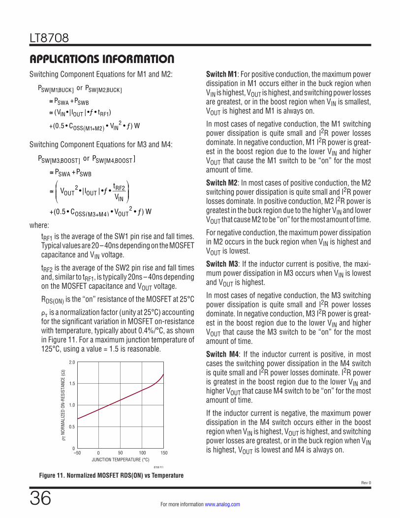
LT8708
36Rev 0
For more information www.analog.com
Figure 11. Normalized MOSFET RDS(ON) vs Temperature
Switching Component Equations for M1 and M2:
PSW[M1,BUCK] or PSW[M2,BUCK]
≅ PSWA +PSWB
≅ (VIN • |IOUT | •ƒ • tRF1)
+(0.5 • COSS M1+M2( ) • VIN2 • ƒ) W
Switching Component Equations for M3 and M4:
PSW[M3,BOOST] or PSW[M4,BOOST ]
≅ PSWA +PSWB
≅ VOUT2 • |IOUT | •ƒ •
tRF2VIN
⎛
⎝
⎜⎜⎜
⎞
⎠
⎟⎟⎟
+(0.5 • COSS M3+M4( ) • VOUT2 • ƒ) W
where: tRF1 is the average of the SW1 pin rise and fall times.
Typical values are 20 – 40ns depending on the MOSFET capacitance and VIN voltage.
tRF2 is the average of the SW2 pin rise and fall times and, similar to tRF1, is typically 20ns – 40ns depending on the MOSFET capacitance and VOUT voltage.
RDS(ON) is the “on” resistance of the MOSFET at 25°C
ρτ is a normalization factor (unity at 25°C) accounting for the significant variation in MOSFET on-resistance with temperature, typically about 0.4%/°C, as shown in Figure 11. For a maximum junction temperature of 125°C, using a value = 1.5 is reasonable.
Switch M1: For positive conduction, the maximum power dissipation in M1 occurs either in the buck region when VIN is highest, VOUT is highest, and switching power losses are greatest, or in the boost region when VIN is smallest, VOUT is highest and M1 is always on.
In most cases of negative conduction, the M1 switching power dissipation is quite small and I2R power losses dominate. In negative conduction, M1 I2R power is great-est in the boost region due to the lower VIN and higher VOUT that cause the M1 switch to be “on” for the most amount of time.
Switch M2: In most cases of positive conduction, the M2 switching power dissipation is quite small and I2R power losses dominate. In positive conduction, M2 I2R power is greatest in the buck region due to the higher VIN and lower VOUT that cause M2 to be “on” for the most amount of time.
For negative conduction, the maximum power dissipation in M2 occurs in the buck region when VIN is highest and VOUT is lowest.
Switch M3: If the inductor current is positive, the maxi-mum power dissipation in M3 occurs when VIN is lowest and VOUT is highest.
In most cases of negative conduction, the M3 switching power dissipation is quite small and I2R power losses dominate. In negative conduction, M3 I2R power is great-est in the boost region due to the lower VIN and higher VOUT that cause the M3 switch to be “on” for the most amount of time.
Switch M4: If the inductor current is positive, in most cases the switching power dissipation in the M4 switch is quite small and I2R power losses dominate. I2R power is greatest in the boost region due to the lower VIN and higher VOUT that cause M4 switch to be “on” for the most amount of time.
If the inductor current is negative, the maximum power dissipation in the M4 switch occurs either in the boost region when VIN is highest, VOUT is highest, and switching power losses are greatest, or in the buck region when VIN is highest, VOUT is lowest and M4 is always on.
APPLICATIONS INFORMATION
JUNCTION TEMPERATURE (°C)–50
ρ T N
ORM
ALIZ
ED O
N-RE
SIST
ANCE
(Ω)
1.0
1.5
150
8708 F11
0.5
00 50 100
2.0

LT8708
37Rev 0
For more information www.analog.com
Gate Resistors: In some cases it can be beneficial to add 1Ω to 10Ω of resistance between some of the NMOS gate pins and their respective gate driver pins on the LT8708 (i.e., TG1, BG1, TG2, BG2). Due to parasitic inductance and capacitance, ringing can occur on SW1 or SW2 when low capacitance MOSFETs are turned on/off too quickly. The ringing can be of greatest concern when operating the MOSFETs or the LT8708 near the rated voltage limits. Additional gate resistance slows the switching speed, minimizing the ringing.
Excessive gate resistance can have two negative side ef-fects on performance:
1. Slowing the switch transition times can also increase power dissipation in the switch. This is described above.
2. Capacitive coupling from the SW1 or SW2 pin to the switch gate node can turn it on when it’s supposed to be off, thus increasing power dissipation. With too much gate resistance, this would happen to the M2 switch when SW1 is rising with positive inductor current and to the M3 switch when SW2 is rising with negative inductor current.
Careful board evaluation should be performed when opti-mizing the gate resistance values. SW1 and SW2 pin ringing can be affected by the inductor current levels, therefore board evaluation should include measurements at a wide range of load currents, VIN and VOUT. When performing PCB measurements of the SW1 and SW2 pins, be sure to use a very short ground post from the PCB ground to the scope probe ground sleeve in order to minimize false inductive voltage readings.
CIN AND COUT SELECTION
VIN and VOUT capacitance is necessary to suppress volt-age ripple caused by discontinuous current moving in and out of the regulator. A parallel combination of capacitors is typically used to achieve high capacitance and low ESR (equivalent series resistance). Dry tantalum, special
polymer, aluminum electrolytic and ceramic capacitors are all available in surface mount packages. Capacitors with low ESR and high ripple current ratings, such as OS-CON and POSCAP are also available.
Ceramic capacitors should be placed near the regulator input and output to suppress high frequency switching spikes. A ceramic capacitor, of at least 1μF at the maximum VINCHIP operating voltage, should also be placed from VINCHIP to GND as close to the LT8708 pins as possible. Due to their excellent low ESR characteristics ceramic capacitors can significantly reduce input ripple voltage and help reduce power loss in the higher ESR bulk capacitors. X5R or X7R dielectrics are preferred, as these materials retain their capacitance over wide voltage and temperature ranges. Many ceramic capacitors, particularly 0805 or 0603 case sizes, have greatly reduced capacitance at the desired operating voltage.
VIN Capacitance: Discontinuous VIN current is highest in the buck region due to the M1 switch toggling on and off. Make sure that the CIN capacitor network has low enough ESR and is sized to handle the maximum RMS current. For buck operation, the VIN RMS current is given by:
I(IN,RMS) ≅ IOUT •
VOUTVIN
•VIN
VOUT– 1 A
This formula has a maximum at VIN = 2•VOUT, where I(IN,RMS) = IOUT/2. This simple worst-case condition is commonly used for design because even significant devia-tions do not offer much relief.
CIN is necessary to reduce the VIN voltage ripple caused by discontinuities and ripple of IIN. The effects of ESR and the bulk capacitance must be considered when choosing the correct capacitor for a given VIN ripple.
The VIN ripple due to the voltage drop across the bulk cap ESRBULK, without having any ceramic capacitance in parallel, is approximately:
∆V(IN,BUCK,BULK) ≅ IOUT •ESRBULK V
APPLICATIONS INFORMATION

LT8708
38Rev 0
For more information www.analog.com
When low ESR ceramic capacitance is added in parallel with the bulk capacitor, the VIN ripple is approximately:
∆V(IN,BUCK,CERAM) ≅
IOUT • VOUTVIN
•ESRCERAM •
1– exp– VOUT
VIN • ƒ •ESRCERAM •CIN–CERAM
⎛
⎝
⎜⎜⎜
⎞
⎠
⎟⎟⎟
⎛
⎝
⎜⎜⎜
⎞
⎠
⎟⎟⎟
V
Add enough ceramic capacitance to make sure ∆V(IN,BUCK,CERAM) is adequate for the application. In a properly designed application, ∆V(IN,BUCK,CERAM) should be much smaller than ∆V(IN,BUCK,BULK) .
VOUT Capacitance: Discontinuous VOUT current is highest in the boost region due to the M4 switch toggling on and off. Make sure that the COUT capacitor network has low enough ESR and is sized to handle the maximum RMS current. For boost operation, the VOUT RMS current is given by:
I(OUT,RMS) ≅ IOUT •
VOUTVIN
– 1 A
This formula has a maximum when VIN is minimum and VOUT is maximum.
COUT is necessary to reduce the VOUT ripple caused by discontinuities and ripple of IOUT. The effects of ESR and the bulk capacitance must be considered when choosing the right capacitor for a given VOUT ripple.
The VOUT ripple due to the voltage drop across the bulk cap ESR without having any ceramic caps in parallel is approximately:
∆V(OUT,BOOST,BULK) ≅VOUT •IOUT
VIN•ESRBULK
∆V(OUT,BUCK,BULK) ≅ IRIPPLE •ESRBULK
With enough ceramic caps added in parallel, the steady state VOUT ripple due to charging and discharging the ceramic COUT is given by the following equations:
∆V(OUT,BOOST,CERAM) ≅
IOUT •ESRCERAM •
1– expVIN – VOUT
VOUT • ƒ •ESRCERAM •COUT–CERAM
⎛
⎝
⎜⎜⎜
⎞
⎠
⎟⎟⎟
⎛
⎝
⎜⎜⎜
⎞
⎠
⎟⎟⎟
V
for VOUT > VIN, and
∆V(OUT,BUCK,CERAM) ≅
VOUT • 1–VOUTVIN
⎛
⎝
⎜⎜⎜
⎞
⎠
⎟⎟⎟
8 •L • ƒ2 •COUT–CERAMV
for VOUT < VIN
Add enough ceramic caps to make sure ∆V(OUT,BOOST,CERAM) and ∆V(OUT,BUCK,CERAM) are adequate for the application. In a properly designed application, ∆V(OUT,BOOST,CERAM) and ∆V(OUT,BUCK,CERAM) should be much smaller than ∆V(OUT,BOOST,BULK) and ∆V(OUT,BUCK,BULK), respectively.
SCHOTTKY DIODE (D1, D2, D3, D4) SELECTION
During forward conduction the Schottky diodes, D2 and D4, shown in Figure 1, conduct during the dead time between the conduction of the power MOSFET switches. They help to prevent the body diodes of synchronous switches M2 and M4 from turning on and storing charge. For example, D4 can significantly reduce reverse-recovery current when M3 turns on, which improves converter efficiency, reduces switch M3 power dissipation, and reduces noise in the inductor current sense resistor (RSENSE). Similarly, during reverse conduction, D1 and D3 conduct during the dead time between the conduction of the power MOSFET switches. In order for the diodes to be effective, the induc-tance between them and the synchronous switch must be as small as possible, mandating that these components be placed very close to the MOSFETs.
APPLICATIONS INFORMATION

LT8708
39Rev 0
For more information www.analog.com
For applications with high input or output voltages (typically >40V) avoid Schottky diodes with excessive reverse-leakage currents, particularly at high tempera-tures. Some ultra-low VF diodes will trade-off increased high temperature leakage current for reduced forward voltage. Diodes D1 and D2 can have reverse voltages in excess of VIN and D3 and D4 can have reverse voltages in excess of VOUT. The combination of high reverse voltage and current can lead to self-heating of the diode. Besides reducing efficiency, this can increase leakage current which increases temperatures even further. Choose pack-ages with lower thermal resistance (θJA) to minimize self heating of the diodes.
TOPSIDE MOSFET DRIVER SUPPLY (CB1, DB1, CB2, DB2)
The top MOSFET drivers (TG1 and TG2) are driven digitally between their respective SW and BOOST pin voltages. The BOOST voltages are biased from floating booststrap capacitors CB1 and CB2, which are normally recharged through external silicon diodes DB1 and DB2 when the respective top MOSFET is turned off. The capacitors are charged to about 6.3V (about equal to GATEVCC) forcing the VBOOST1-SW1 and VBOOST2-SW2 voltages to be about 6.3V. The boost capacitors CB1 and CB2 need to store about 100 times the gate charge required by the top switches M1 and M4. In most applications, a 0.1μF to 0.47μF, X5R or X7R dielectric capacitor is adequate. The bypass capacitance from GATEVCC to GND should be at least 10 times the CB1 or CB2 capacitance.
Top Driver: Boost Cap Charge Control Block
When the LT8708 operates exclusively in the boost or buck region, M1 or M4 respectively may be “on” continuously. This prevents the respective bootstrap capacitor, CB1 or CB2, from being recharged through the silicon diode, DB1 or DB2. The Boost Cap Charge Control block (see Figure 1) keeps the appropriate bootstrap capacitor charged in these cases. In the boost region, when M1 is always on, current is drawn, as needed, from the CSNOUT and/or BOOST2 pins to charge the CB1 capacitor. In the buck region, when M4 is always on, current is drawn, as needed, from the CSNIN and/or BOOST1 pins to charge the CB2 capacitor.
Because of this function, CSPIN and CSNIN should be connected across RSENSE1 in series with the M1 drain. Connect both pins to the M1 drain if they are not being used. Also, CSPOUT and CSNOUT should be connected across RSENSE2 in series with the M4 drain or connect both to the M4 drain if not being used.
Top Driver: Boost Diodes DB1 and DB2
Although Schottky diodes have the benefit of low forward voltage drops, they can exhibit high reverse current leak-age and have the potential for thermal runaway under high voltage and temperature conditions. Silicon diodes are thus recommended for diodes DB1 and DB2. Make sure that DB1 and DB2 have reverse breakdown voltage ratings higher than VIN(MAX) and VOUT(MAX) and have less than 1mA of reverse-leakage current at the maximum operating junction temperature. Make sure that the reverse-leakage current at high operating temperatures and voltages won’t cause thermal runaway of the diode.
In some cases it is recommended that up to 5Ω of resistance is placed in series with DB1 and DB2. The resistors reduce surge currents in the diodes and can reduce ringing at the SW and BOOST pins of the IC. Since SW pin ringing is highly dependent on PCB layout, SW pin edge rates and the type of diodes used, careful measurements directly at the SW pins of the IC are recommended. If required, a single resistor can be placed between GATEVCC and the common anodes of DB1 and DB2 (as in the front page application) or by placing separate resistors between the cathodes of each diode and the respective BOOST pins. Excessive resistance in series with DB1 and DB2 can reduce the BOOST-SW capacitor voltage when the M2 or M3 on-times are very short and should be avoided.
VINHIMON, VOUTLOMON AND RVSOFF
During reverse conduction, current and power are drawn from VOUT and delivered to VIN. This has the potential to draw VOUT lower than desired or drive VIN higher than desired, depending on the supplies and loads. The VIN-HIMON and VOUTLOMON pins are used to detect either of these conditions and disable reverse conduction by pulling RVSOFF low.
APPLICATIONS INFORMATION

LT8708
40Rev 0
For more information www.analog.com
The purpose of the VINHIMON and VOUTLOMON func-tions becomes clearer when considering the priorities of the error amplifiers (see Table 3). A few important cases should be considered.
1. VIN and VOUT are both above regulation: In this case FBIN is greater than 1.205V while FBOUT is greater than 1.207V. Normally this condition causes VC to fall due to FBOUT being above 1.207V. The LT8708 responds by increasing the reverse current and power being fed into VIN.
This can be an undesirable response, for example, if VIN is connected to a battery being charged from VOUT. The solution is to use VINHIMON to detect the maximum VIN and disable reverse conduction by pull-ing RVSOFF low.
2. VIN and VOUT are both below regulation: In this case FBIN is below 1.205V while FBOUT is below 1.207V. Normally this condition causes VC to fall due to FBIN being below 1.205V. The LT8708 responds by in-creasing the reverse current and power being drawn from VOUT.
This can be an undesirable response, for example, if VOUT is connected to a battery or supercapacitor sup-plying power to VIN. The solution is to use VOUTLO-MON to detect the minimum VOUT and disable reverse conduction by pulling RVSOFF low.
If VINHIMON rises above its activation threshold or VOUT-LOMON falls below its activation threshold (see Electrical Characteristics), the LT8708 will pull the RVSOFF pin low and not allow M4 switch to turn on if the inductor cur-rent is negative. In addition to the 24mV (typical) voltage hysteresis, the VINHIMON pin will source 1μA (typical) current and the VOUTLOMON pin will sink 1μA (typical) current as current hysteresis.
There are two ways to configure the VINHIMON and VOUTLOMON pins. Method (1) uses dedicated resistor dividers for VINHIMON and VOUTLOMON respectively, while method (2) uses common resistor dividers for VINHIMON and FBIN as well as for VOUTLOMON and FBOUT, allowing improved tracking with the FBOUT and FBIN regulation voltages, respectively.
1. Connect a resistor divider between VIN, VINHIMON and GND to configure the VIN overvoltage threshold. Connect a resistor divider between VOUT, VOUTLO-MON and GND to configure the VOUT undervoltage threshold. (see Figure 12). Use the following equa-tions to calculate the resistor values:
RHIMON1=VOVIN+ – 1.207
IFBDIV
RHIMON2 =1.207IFBDIV
RHIMON3 =1.207 – VHYSMON
IHYSMON
⎛
⎝
⎜⎜⎜
⎞
⎠
⎟⎟⎟ –
RHIMON1 •RHIMON2RHIMON1+RHIMON2
⎛
⎝
⎜⎜⎜
⎞
⎠
⎟⎟⎟
–VOVIN
– •RHIMON2IHYSMON •(RHIMON1+RHIMON2)
⎛
⎝
⎜⎜⎜
⎞
⎠
⎟⎟⎟
RLOMON1=VUVOUT – – 1.207
IFBDIV
RLOMON2 =1.207IFBDIV
RLOMON3 =VUVOUT+ •RLOMON2
IHYSMON •(RLOMON1+RLOMON2)
⎛
⎝
⎜⎜⎜
⎞
⎠
⎟⎟⎟
–RLOMON1 •RLOMON2RLOMON1+RLOMON2
⎛
⎝
⎜⎜⎜
⎞
⎠
⎟⎟⎟ –
1.207 + VHYSMONIHYSMON
⎛
⎝
⎜⎜⎜
⎞
⎠
⎟⎟⎟
where:
IFBDIV is the desired current through the resistor string. 50μA – 100μA is a good value.
VOVIN+ and VOVIN– are the rising and falling VIN over-voltage thresholds.
VUVOUT+ and VUVOUT– are the rising and falling VOUT undervoltage thresholds.
RHIMON1-3 and RLOMON1-3 are shown in Figure 12.
VHYSMON is the VINHIMON and VOUTLOMON hyster-esis voltage. Typical value is 24mV.
IHYSMON is the VINHIMON and VOUTLOMON hysteresis current. Typical value is 1μA.
APPLICATIONS INFORMATION
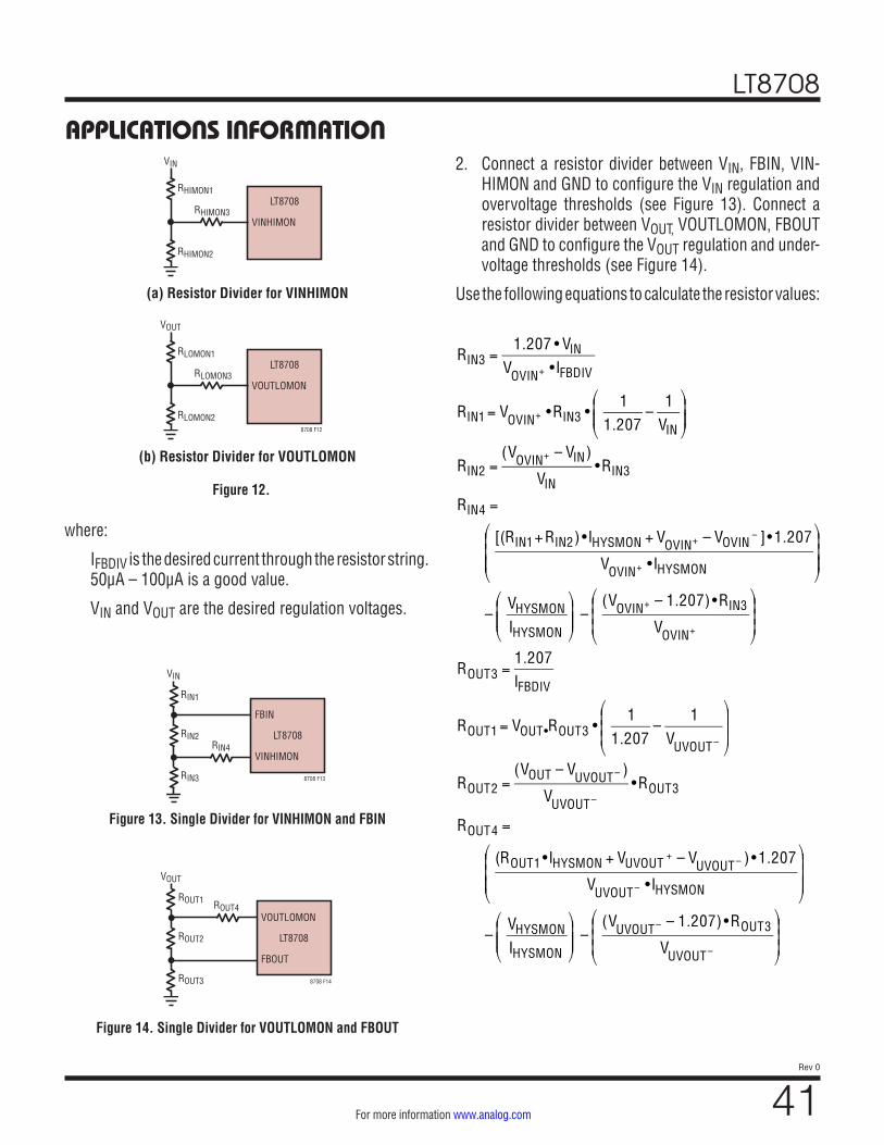
LT8708
41Rev 0
For more information www.analog.com
2. Connect a resistor divider between VIN, FBIN, VIN-HIMON and GND to configure the VIN regulation and overvoltage thresholds (see Figure 13). Connect a resistor divider between VOUT, VOUTLOMON, FBOUT and GND to configure the VOUT regulation and under-voltage thresholds (see Figure 14).
Use the following equations to calculate the resistor values:
RIN3 =1.207 • VIN
VOVIN+ •IFBDIV
RIN1= VOVIN+ •RIN3 •1
1.207–
1VIN
⎛
⎝
⎜⎜⎜
⎞
⎠
⎟⎟⎟
RIN2 =(VOVIN+ – VIN)
VIN•RIN3
RIN4 =
[(RIN1+RIN2) •IHYSMON + VOVIN+ – VOVIN– ]•1.207
VOVIN+ •IHYSMON
⎛
⎝
⎜⎜⎜⎜
⎞
⎠
⎟⎟⎟⎟
–VHYSMONIHYSMON
⎛
⎝
⎜⎜⎜
⎞
⎠
⎟⎟⎟ –
(VOVIN+ – 1.207) •RIN3
VOVIN+
⎛
⎝
⎜⎜⎜
⎞
⎠
⎟⎟⎟
ROUT3 =1.207IFBDIV
ROUT1= VOUT•ROUT3 •1
1.207–
1VUVOUT –
⎛
⎝
⎜⎜⎜
⎞
⎠
⎟⎟⎟
ROUT2 =(VOUT – VUVOUT – )
VUVOUT –•ROUT3
ROUT4 =
(ROUT1 •IHYSMON + VUVOUT+ – VUVOUT – ) •1.207
VUVOUT – •IHYSMON
⎛
⎝
⎜⎜⎜⎜
⎞
⎠
⎟⎟⎟⎟
–VHYSMONIHYSMON
⎛
⎝
⎜⎜⎜
⎞
⎠
⎟⎟⎟ –
(VUVOUT – – 1.207) •ROUT3
VUVOUT –
⎛
⎝
⎜⎜⎜
⎞
⎠
⎟⎟⎟
where:
IFBDIV is the desired current through the resistor string. 50μA – 100μA is a good value.
VIN and VOUT are the desired regulation voltages.
APPLICATIONS INFORMATION
Figure 12.
Figure 13. Single Divider for VINHIMON and FBIN
RIN4
FBIN
VINHIMON
LT8708
8708 F13
VIN
RIN1
RIN2
RIN3
ROUT4VOUTLOMON
FBOUT
LT8708
8708 F14
VOUT
ROUT1
ROUT2
ROUT3
VINHIMON
LT8708
VIN
RHIMON1
RHIMON3
RHIMON2
VOUTLOMON
LT8708
8708 F12
VOUT
RLOMON1
RLOMON3
RLOMON2
(a) Resistor Divider for VINHIMON
(b) Resistor Divider for VOUTLOMON
Figure 14. Single Divider for VOUTLOMON and FBOUT

LT8708
42Rev 0
For more information www.analog.com
VOVIN+ and VOVIN– are the rising and falling VIN over-voltage thresholds.
VUVOUT+ and VUVOUT– are the rising and falling VOUT undervoltage thresholds.
RIN1-4 and ROUT1-4 are shown in Figure 13 and Figure 14.
VHYSMON is the VINHIMON and VOUTLOMON hyster-esis voltage. Typical value is 24mV.
IHYSMON is the VINHIMON and VOUTLOMON hysteresis current. Typical value is 1μA.
If unused, tie VINHIMON to GND and/or VOUTLOMON to LDO33.
Note: after the resistor values are selected, make sure to check that the FBIN and VOUTLOMON voltages are be-low their ABSMAX values when VIN and VOUT are at their maximum, respectively.
IIN AND IOUT CURRENT MONITORING AND LIMITING
The LT8708 has independent IIN and IOUT current monitors that can monitor and limit the respective currents in both positive and negative directions. Figure 15 and Figure 16 illustrate the operation of the current monitor circuits.
The remaining discussion refers to the IIN current monitor circuit of Figure 15. All discussion and equations are also applicable to the IOUT current monitor circuit, substituting pin and device names as appropriate.
Current Monitoring: The IMON_INP and IMON_INN pins can be used to monitor IIN in the forward and reverse directions, respectively. When configured as shown in Figure 15, the IMON_INP and IMON_INN voltages are proportional to IIN. VIMON_INP is proportional to the posi-tive IIN current, increasing as IIN becomes more positive. VIMON_INN is proportional to the negative IIN current, increasing as IIN becomes more negative.
APPLICATIONS INFORMATION
Figure 16. IOUT Current Monitor and Limit
–
+EA1
IMON_INPIMON_INN8708 F15
CIMON_INPRIMON_INP
CSPIN
RSENSE1FROM
SYSTEMVIN
TOCONTROLLERVIN
CSNINLT8708
IIN
VC
1.21V
–
+EA5
1.209V
–+gm = 1m
Ω
A3
CIMON_INNRIMON_INN
+–20μA
20μA
–
+EA2
IMON_OPIMON_ON8708 F16
CIMON_OPRIMON_OP
CSPOUT
RSENSE2FROM
CONTROLLERVOUT
TOSYSTEMVOUT
CSNOUTLT8708
IOUT
VC
1.21V
–
+EA6
1.209V
–+gm = 1m
Ω
A1
CIMON_ONRIMON_ON
+–20μA
20μA
Figure 15. IIN Current Monitor and Limit

LT8708
43Rev 0
For more information www.analog.com
Transconductance amplifier A3 performs this monitoring function. A3 converts the current sense voltage, VCSPIN-CSNIN, into two currents:
+VCSPIN-CSNIN •1m
AV
and
– VCSPIN-CSNIN •1m
AV
These currents are added to 20μA offsets and then forced into RIMON_INP and RIMON_INN, respectively.
Due to the 20μA offset currents, VIMON_INP and VIMON_INN are not 0V when IIN is 0A. Instead, VIMON_INP(0) = 20μA•RIMON_INP Volts and VIMON_INN(0) = 20μA•RIMON_INN Volts (typical) when IIN = 0 Amps. As IIN becomes increas-ingly negative, VIMON_INP reduces below VIMON_INP(0) until VIMON_INP = 0V. Similarly, as IIN becomes increas-ingly positive, VIMON_INN reduces below VIMON_INN(0) until VIMON_INN = 0V. IMON_INP and IMON_INN will not be driven below ground as their output currents can only be positive or zero.
The complete transfer functions for IMON_INP and IMON_INN are given in the equations below:
VIMON _INP = 1mAV
•RSENSE1 •IIN + 20µA⎛
⎝⎜⎜
⎞
⎠⎟⎟ •RIMON _INP
VIMON _INN = –1mAV
•RSENSE1 •IIN + 20µA⎛
⎝⎜⎜
⎞
⎠⎟⎟ •RIMON _INN
The differential voltage VCSPIN-CSNIN should remain be-tween –100mV and 100mV due to the limited current that can be driven out of IMON_INP and IMON_INN. If the instantaneous VCSPIN-CSNIN exceeds these limits but the average VCSPIN-CSNIN is within the limits, consider includ-ing the current sense filter described in the next section.
In addition, IMON_INP and IMON_INN should be filtered with capacitors CIMON_INP and CIMON_INN due to IIN ripple and discontinuities that can occur in various regions of operation. A few nF of capacitance is usually sufficient.
APPLICATIONS INFORMATIONCurrent Limiting: As shown in Figure 15, IMON_INP voltage that exceeds 1.209V (typical) causes VC to reduce, thus limiting the forward IIN and inductor currents. IMON_INN voltage that exceeds 1.21V (typical) causes VC to increase, thus limiting the reverse IIN and inductor currents (see the Error Amplifiers section).
The forward IIN limit, I(IN,FWD,LIMIT), can be set as needed by choosing the appropriate RSENSE1 and RIMON_INP resis-tors using the following equation:
RIMON _INP =
1.209
I(IN,FWD,LIMIT) •1mAV
•RSENSE1+ 20µAΩ
For example, if RSENSE1 is chosen to be 12.5mΩ and the desired forward IIN current limit is 4A then:
RIMON _INP =
1.209
4A •1mAV
•12.5mΩ + 20µA= 17.3kΩ
Similarly, the reverse IIN limit, I(IN,RVS,LIMIT), can be set as needed by choosing the appropriate RSENSE1 and RIMON_INN resistors using the following equation:
RIMON _INN =
1.21
I(IN,RVS,LIMIT) •1mAV
•RESENSE1+ 20µAΩ
CIMON_INP and CIMON_INN capacitors of at least a few nF are necessary to maintain loop stability when IMON_INP and IMON_INN, respectively, are used to operate the LT8708 at constant current limit.
Review the Electrical Characteristics and the IMON Output Currents graph in the Typical Performance Characteris-tics section to understand the operational limits of the IMON_OP, IMON_ON, IMON_INP and IMON_INN currents.
External currents can be summed to the IMON pins to adjust IIN and/or IOUT limit in both directions while switch-ing. When the IMON_OP and IMON_ON pins are used in

LT8708
44Rev 0
For more information www.analog.com
Figure 17. CSPIN/CSNIN and CSPOUT/CSNOUT Current Sense Filter
CSPIN CSNIN
LT8708
CFILTER1
RFILTER1
RSENSE1
CSPOUT CSNOUT
LT8708
8708 F17
CFILTER2
RFILTER2
RSENSE2
this way, ICP and ICN can be used to monitor the IOUT current in the forward and reverse directions respectively (see the Current Monitoring, Regulation and Limiting: ICP and ICN Pins section).
Current Sense Filter: The + and – outputs of current sense amplifiers A1 and A3 are rated to provide a range of –20μA to +100μA. For example, IMON_INP, which primarily reports forward IIN current, may not provide the expected output current when VCSPIN-CSNIN exceeds 100mV. In addition, the IMON_INP pin will not provide the expected output current when VCSPIN-CSNIN is below –20mV.
Currents that flow through the current sense resistors (RSENSE1, RSENSE2 in Figure 17) are often discontinu-ous and can contain significant AC content during each switching cycle. One example is the forward IIN in the buck region. If the IIN current presents an average differential (VCSPIN-CSNIN) less than 100mV, but contains AC peaks exceeding 100mV, the IMON_INP current may clip. To prevent clipping, the current sense filter shown in Figure 17, can be added. The filter will reduce the peak differ-ential (VCSPIN-CSNIN) to <100mV while keeping the same average, thus allowing the correct result to be presented on IMON_INP. As another example, consider the reverse IOUT measured by IMON_ON. If the current presents an average differential (VCSNOUT-CSPOUT) less than 100mV, but contains AC peaks exceeding 100mV, the current sense filter can be used to reduce the peaks below 100mV while keeping the same average.
The –20μA output current limits for amplifiers A1 and A3 are often most important when using the HCM mode (see the Unidirectional Conduction: HCM section). The current
sense amplifier outputs may clip at the –20μA limits when the average sensed current is low but contains high AC content. Clipping may distort the ICN or IMON_INP voltages that are used to select between heavy and light load HCM operation. Once again, the current sense filter can be used to reduce the AC content appearing at the amplifier inputs.
Current sense filter(s) should be connected as shown in Figure 16. Note that resistance in series with CSNIN and CSNOUT is not recommended. As described in the Topside MOSFET Driver Supply (CB1, DB1, CB2, DB2) section, the CSNIN and CSNOUT pins are also connected to the Boost Cap Charge Control block (also see Figure 1) and can draw current under certain conditions. In addition, the same CSNIN and CSNOUT current sense pins can draw bias cur-rent under normal operating conditions, while CSPIN and CSPOUT draw zero (typical) bias current. A time constant lower than 10μs is recommended for the filter(s).
Also, because of their use with the Boost Cap Charge Control block, tie the CSPIN and CSNIN pins to VIN and tie the IMON_INP and IMON_INN pins to ground when the input current sensing is not in use. Similarly, the CSPOUT and CSNOUT pins should be tied to VOUT, the IMON_OP, IMON_ON pins should be grounded when not in use.
LOOP COMPENSATION
The loop stability is affected by a number of factors includ-ing the inductor value, output capacitance, load current, VIN, VOUT and the VC resistor and capacitors. The LT8708 uses internal transconductance error amplifiers driving VC to help compensate the control loop. For most applications a 3.3nF series capacitor at VC is a good value. The parallel capacitor (from VC to GND) is typically 1/10th the value of the series capacitor to filter high frequency noise. A larger VC series capacitor value may be necessary if the output capacitance is reduced. A good starting value for the VC series resistor is 20k. Lower resistance will improve stability but will slow the loop response. Use a trim pot instead of a fixed resistor for initial bench evaluation to determine the optimum value.
Also note that CIMON_INP and CIMON_INN capacitors of at least a few nF are necessary to maintain loop stability
APPLICATIONS INFORMATION

LT8708
45Rev 0
For more information www.analog.com
when IMON_INP and IMON_INN, respectively, are used to operate the LT8708 at constant current limit.
INTVCC REGULATORS AND EXTVCC CONNECTION
The LT8708 features two PNP LDOs (low dropout regu-lators) that regulate the 6.35V (typical) INTVCC pin from either the VINCHIP or EXTVCC supply pin. INTVCC powers the MOSFET gate drivers via the required GATEVCC connec-tion and also powers the LDO33 pin regulator and much of the LT8708’s internal control circuitry. The INTVCC LDO selection is determined automatically by the EXTVCC pin voltage. When EXTVCC is lower than 6.2V (typical), INTVCC is regulated from the VINCHIP pin LDO. After EXTVCC rises above 6.4V (typical), INTVCC is regulated by the EXTVCC pin LDO instead.
Overcurrent protection circuitry typically limits the maximum current draw from either LDO to 127mA. When GATEVCC and INTVCC are below 4.65V, during start-up or during an overload condition, the typical current limit is reduced to 42mA. The INTVCC pin must be bypassed to ground with a minimum 4.7μF ceramic capacitor placed as close as possible to the INTVCC and GND pins. An ad-ditional ceramic capacitor should be placed as close as possible to the GATEVCC and GND pins to provide good bypassing to supply the high transient current required by the MOSFET gate drivers. 1μF to 4.7μF is recommended.
Power dissipated in the INTVCC LDOs must be minimized to improve efficiency and prevent overheating of the LT8708. Since LDO power dissipation is proportional to the supply voltage and VINCHIP can be as high as 80V in some applica-tions, the EXTVCC pin is available to regulate INTVCC from a lower supply voltage. The EXTVCC pin is connected to VOUT in many applications since VOUT is often regulated to a much lower voltage than the maximum VINCHIP. During start-up, power for the MOSFET drivers, control circuits and the LDO33 pin is usually derived from VINCHIP until VOUT/EXTVCC rises above 6.4V, after which the power is derived from VOUT/EXTVCC. This works well, for example, in a case where VOUT is regulated to 12V and the maximum VINCHIP voltage is 40V. EXTVCC can be floated or grounded when not in use or can also be connected to an external power supply if available.
The following list summarizes the three possible connec-tions for EXTVCC:
1. EXTVCC left open (or grounded). This will cause INTVCC to be powered from VINCHIP through the internal 6.3V regulator at the cost of a small efficiency penalty.
2. EXTVCC connected directly to VOUT (VOUT > 6.4V). This is the normal connection for the regulator and usually provides the highest efficiency.
3. EXTVCC connected to an external supply. If an external supply is available greater than 6.4V (typical) it may be used to power EXTVCC.
Powering INTVCC from EXTVCC can also provide enough gate drive when VINCHIP drops as low as 2.8V. This allows the part to operate with a reduced VINCHIP voltage after VOUT gets into regulation.
The maximum current drawn through the INTVCC LDO occurs under the following conditions:
1. Large (capacitive) MOSFETs are being driven at high frequencies.
2. VIN and/or VOUT is high, thus requiring more charge to turn the MOSFET gates on and off.
3. The LDO33 pin output current is high.
4. In some applications, LDO current draw is maximum when the part is operating in the buck-boost region where VIN is close to VOUT since all four MOSFETs are switching.
To check for overheating find the operating conditions that consume the most power in the LT8708 (PLT8708). This will often be under the same conditions just listed that maximize LDO current. Under these conditions monitor the CLKOUT pin duty cycle to measure the approximate die temperature. See the Junction Temperature Measurement section for more information.
LDO33 REGULATOR
The LT8708 includes a low dropout regulator (LDO) to regulate the LDO33 pin to 3.3V. This pin can be used to power external circuitry such as a microcontroller or other desired peripherals. The input supply for the LDO33 pin
APPLICATIONS INFORMATION

LT8708
46Rev 0
For more information www.analog.com
regulator is INTVCC. Therefore INTVCC must have sufficient voltage, typically > 4.0V, to properly regulate LDO33. The LDO33 and INTVCC regulators are enabled by the SHDN pin and are not affected by SWEN. The LDO33 pin regu-lator has overcurrent protection circuitry that typically limits the output current to 17.25mA. An undervoltage lockout monitors LDO33 and disables switching activity when LDO33 falls below 3.04V (typical). LDO33 should be bypassed locally with 0.1μF or more.
VOLTAGE LOCKOUTS
The LT8708 contains several voltage detectors to make sure the chip is under proper operating conditions. Table 8 summarizes the pins that are monitored and also indi-cates the state that the LT8708 will enter if an under or over voltage condition is detected. Table 8. Voltage Lockout Conditions
PIN(S)
APPROXIMATE VOLTAGE
CONDITIONCHIP STATE (Figure 2) READ SECTION
VINCHIP <2.5VCHIP OFF
Operation: Start-Up
SHDN <1.18V
INTVCC and GATEVCC
<4.65VSWITCHER
OFF 1SWEN <1.18V
LDO33 <3.04V
VINHIMON >1.207V
–
Applications Information: VINHIMON,
VOUTLOMON and RVSOFF
VOUTLOMON <1.207V
RVSOFF <1.209V
FBIN <1.205V Voltage Lockouts
The conditions are listed in order of priority from top to bottom. If multiple over/undervoltage conditions are detected, the chip will enter the state listed highest on the table.
Due to their accurate thresholds, configurable undervoltage lockouts (UVLOs) can be implemented using the SHDN and SWEN and in some cases, FBIN pin. The UVLO function sets the turn on/off of the LT8708 at a desired minimum voltage. For example, a resistor divider can be connected between VIN, SHDN and GND as shown in Figure 1. From the Electrical Characteristics, SHDN has typical rising and
falling thresholds of 1.221V and 1.181V, respectively. The falling threshold for turning-off switching activity can be chosen using:
RSHDN1=
RSHDN2 •(V(IN,CHIPOFF,FALLING) – 1.181)
1.181Ω
For example, choosing RSHDN2 = 20k and a falling VIN threshold of 5.42V results in:
RSHDN1=
20k •(5.42 – 1.181)1.181
≅ 71.5kΩ
The rising threshold for enabling switching activity would be:
V(IN,CHIPOFF,RISING) = V(IN,CHIPOFF,FALLING) •
1.2211.181
or 5.6V in this example.
Similar calculations can be used to select a resistor divider connected to SWEN that would stop switching activity dur-ing an undervoltage condition. Make sure that the divider doesn’t cause SWEN to exceed 7V (ABSMAX rating) under maximum supply voltage conditions. See the Start-Up: SWEN Pin section for additional information.
The same technique described in the VIN: Regulation section can be used to create an undervoltage lockout if the LT8708 is in forward non-CCM mode, where forcing VC low will stop all switching activity. Note that this does not reset the soft-start function, therefore resumption of switching activity will not be accompanied by a soft-start.
JUNCTION TEMPERATURE MEASUREMENT
The duty cycle of the CLKOUT signal is linearly proportional to the die junction temperature, TJ. Measure the duty cycle of the CLKOUT signal and use the following equation to approximate the junction temperature:
TJ ≅
DCCLKOUT – 34.4%0.325%
°C
APPLICATIONS INFORMATION

LT8708
47Rev 0
For more information www.analog.com
where DCCLKOUT is the CLKOUT duty cycle in % and TJ is the die junction temperature in °C. The actual die tem-perature can deviate from the above equation by ±10°C.
THERMAL SHUTDOWN
If the die junction temperature reaches approximately 165°C, the part will go into thermal shutdown. The power switches will be turned off and the INTVCC and LDO33 regulators will be turned off (see Figure 2). The part will be re-enabled when the die temperature has dropped by ~5°C (nominal). After re-enabling, the part will start in the SWITCHER OFF 1 state as shown in Figure 2. The part will then INITIALIZE, perform a SOFT-START, then enter NORMAL OPERATION as long as the die temperature remains below approximately 165°C.
EFFICIENCY CONSIDERATIONS
The efficiency of a switching regulator is equal to the output power divided by the input power times 100%. It is often useful to analyze individual losses to determine what is limiting the efficiency and which change would produce the most improvement. Although all dissipative elements in the circuit produce losses, three main sources account for most of the losses in LT8708 circuits. These and a few additional loss components are listed below:
1. Switching losses. These losses arise from the brief amount of time the switches (M1 – M4) spend in the saturated region during switch node transitions. Power loss depends upon the input voltage, load current, driver strength and MOSFET capacitance, among other factors. See the Power MOSFET Selection section for more details.
2. DC I2R losses. These arise from the resistances of the MOSFETs (M1 – M4), sensing resistors, inductor and PC board traces and cause the efficiency to drop at high currents.
3. INTVCC current. This is the sum of the MOSFET driver current, LDO33 pin current and control currents. The INTVCC regulator’s input voltage times the current represents lost power. This loss can be reduced by supplying INTVCC current through the EXTVCC pin
APPLICATIONS INFORMATIONfrom a high efficiency source, such as the output or alternate supply if available. Also, lower capacitance MOSFETs can reduce INTVCC current and power loss.
4. CIN and COUT loss. The CIN capacitor has the difficult job of filtering the large RMS input current to the regulator in buck mode. The COUT capacitor has the more difficult job of filtering the large RMS output current in boost mode. Both CIN and COUT are required to have low ESR to minimize the AC I2R loss and have sufficient capacitance to prevent the RMS current from causing additional upstream losses in fuses or batteries.
5. Other losses. Schottky diodes D1, D2, D3 and D4 are responsible for conduction losses during dead time and light load conduction periods. Inductor core loss occurs predominately at light loads.
Hybrid conduction mode (HCM) can be used to improve the efficiency when large inductor current ripples are present in DCM. See the Unidirectional Conduction: HCM section for details.
When making adjustments to improve efficiency, the input current is the best indicator of changes in efficiency. If one makes a change and the input current decreases, then the efficiency has increased. If there is no change in input current, then there is no change in efficiency.
CIRCUIT BOARD LAYOUT CHECKLIST
The basic circuit board layout requires a dedicated ground plane layer. Also, for high current, a multilayer board pro-vides heat sinking for power components.
• The ground plane layer should not have any traces and should be as close as possible to the layer with the power MOSFETs.
• The high di/dt path formed by switch M1, switch M2, D1, RSENSE and the CIN capacitor should be compact with short leads and PC trace lengths. The high di/dt path formed by switch M3, switch M4, D2 and the COUT capacitor also should be compact with short leads and PC trace lengths. Two layout examples are shown in Figure 18 (a) and (b).

LT8708
48Rev 0
For more information www.analog.com
Figure 18. Switches Layout
• Avoid running signal traces parallel to the traces that carry high di/dt current because they can receive inductively coupled voltage noise. This includes the SW1, SW2, TG1 and TG2 traces to the controller.
• Use immediate vias to connect the components (in-cluding the LT8708’s GND pins) to the ground plane. Use several vias for each power component.
• Minimize parasitic SW pin capacitance by removing GND, VIN and VOUT copper from underneath the SW1 and SW2 regions.
• Except under the SW pin regions, flood all unused areas on all layers with copper. Flooding with copper will reduce the temperature rise of power components. Connect the copper areas to a DC net (i.e., quiet GND) with many vias. The more vias the board has, the better heat conduction it has.
• Partition the power ground from the signal ground. The small-signal component grounds should not return to the IC GND through the power ground path.
• Place switch M2 and switch M3 as close to the controller as possible, keeping the GND, BG and SW traces short.
• Minimize inductance from the sources of M2 and M3 to RSENSE by making the trace short and wide.
• Keep the high dv/dt nodes SW1, SW2, BOOST1, BOOST2, TG1 and TG2 away from sensitive small-signal nodes.
• The output capacitor (–) terminals should be connected as closely as possible to the (–) terminals of the input capacitor.
• Connect the top driver boost capacitor CB1 closely to the BOOST1 and SW1 pins. Connect the top driver boost capacitor CB2 closely to the BOOST2 and SW2 pins.
• Connect the CIN and COUT capacitors closely to the power MOSFETs. These capacitors carry the MOSFET AC current in the boost and buck regions.
• Connect the FBOUT, FBIN, VINHIMON and VOUTLO-MON pin resistor dividers to the (+) terminals of COUT and CIN, respectively. Small FBOUT/FBIN/VINHIMON/VOUTLOMON bypass capacitors may be connected closely to the LT8708’s GND pin if needed. The resistor connections should not be along the high current or noise paths.
• Route current sense traces (CSP/CSN, CSPIN/CSNIN, CSPOUT/CSNOUT) together with minimum PC trace
APPLICATIONS INFORMATION
GND
VOUT
COUT
L
RSENSE
8708 F18
M4
M3M2
M1
SW1 SW2
D2
D4D1
VIN
CIN
LT8708CKT
D3
M3 M4M1 M2
LT8708CKT
D4D2D1 D3
VOUTVIN SW1 SW2
L
RSENSE
GND
COUTCIN
18(a)
18(b)

LT8708
49Rev 0
For more information www.analog.com
spacing. Avoid having sense lines pass through noisy areas, such as switch nodes. The optional filter network capacitor between CSP and CSN should be as close as possible to the IC. Ensure accurate current sensing with Kelvin connections at the RSENSE resistors.
• Connect the VC pin compensation network closely to the IC, between VC and the signal ground pins. The capacitor helps to filter the effects of PCB noise and output voltage ripple voltage from the compensa-tion loop.
• Connect the INTVCC and GATEVCC bypass capacitors close to the IC. The capacitors carry the MOSFET drivers’ current peaks.
• Run the trace from the LT8708’s SW1/SW2 pin to the drain of M2/M3 in parallel with the trace from the GATEVCC capacitor’s GND to the CIN GND. Route the traces (as much as possible) directly above/below one another on adjacent layers and in such a way that they carry currents in opposite directions.
• Attention is required when making the PCB layout for RSENSE1 and RSENSE2, especially for sense resistor values smaller than 5mΩ. Improper PCB layout can yield significant errors in the sense voltage.
HOT PLUGGING CONSIDERATIONS
When connecting a battery to an LT8708 application, there can be significant inrush current due to charge equalization between the partially charged battery stack and the charger output capacitors. To a lesser extent a similar effect can occur when connecting a powered DC supply to the input or output. The magnitude of the inrush current depends on (1) the battery or supply voltage, (2) ESR of the input or output capacitors, (3) initial voltage of the capacitors, and (4) cable impedance. Excessive inrush current can lead to sparking that can compromise connector integrity and/or voltage overshoot that can cause electrical overstress on LT8708 pins.
Excessive inrush current can be mitigated by first con-necting the battery or supply to the charger through a resistive path, followed quickly by a short circuit. This can be accomplished using staggered length pins in a
APPLICATIONS INFORMATIONmulti-pin connector. Alternatively, consider the use of a Hot Swap controller such as the LT1641, LT4256, etc. to make a current limited connection.
DESIGN EXAMPLE
VIN = 8V to 25V
VIN_FBIN = 12V (VIN regulation voltage set by FBIN loop)
VOUT_FBOUT = 12V (VOUT regulation voltage set by FBOUT loop)
IOUT(MAX,FWD) = 5A
IIN(MAX,RVS) = 3A
ƒ = 150kHz
This design operates in CCM.
Maximum ambient temperature = 60°C
Power Flow Verification: Determine which conditions in Table 6(a) apply to this application. In this design example, the VINHIMON and VOUTLOMON are disabled, therefore the conditions highlighted in blue in the copy of Table 6(a) apply to this application.Table 9. A Copy of Table 6(a)
VOUT < VOUT_VOUTLOMON
VOUT > VOUT_VOUTLOMON & VOUT < VOUT_FBOUT
VOUT > VOUT_FBOUT
VIN < VIN_FBINNo Power Transfer B B
VIN > VIN_FBIN & VIN <
VIN_VINHIMON
A D C
VIN > VIN_VINHIMON
A D No Power Transfer
Next, check each of these highlighted cells using Table 6(b) with MODE = CCM. A copy of Table 6(b) is shown below:
9(b). A Copy of Table 6(b)
MODE = BURST MODE = CCM
MODE = DCM/HCM, DIR = FWD
MODE = DCM/HCM, DIR = RVS
A Power Flows from VIN to VOUT No Power Flow
B No Power Flow
Power Flows from VOUT to VIN
No Power Flow
Power Flows from VOUT to VIN
CNo Power FlowD Power Flows from VIN to VOUT

LT8708
50Rev 0
For more information www.analog.com
Verify expected operation by combining Table 6(a) and Table 6(b):
• When VIN < VIN_FBIN (12V) and VOUT > VOUT_FBOUT (12V)
B – power is transferred from VOUT to VIN
• When VIN < VIN_FBIN (12V) and VOUT < VOUT_FBOUT (12V)
B – power is transferred from VOUT to VIN
• When VIN > VIN_FBIN (12V) and VOUT > VOUT_FBOUT (12V)
C – power is transferred from VOUT to VIN
• When VIN > VIN_FBIN (12V) and VOUT < VOUT_FBOUT (12V)
D – power is transferred from VIN to VOUT
The results above are as expected for this design example.
RT Selection: Choose the RT resistor for the free-running oscillator frequency using:
RT =
43,750fOSC
– 1⎛
⎝
⎜⎜⎜
⎞
⎠
⎟⎟⎟ kΩ =
43,750150
– 1⎛
⎝⎜⎜
⎞
⎠⎟⎟ = 290.7kΩ
We will choose 294k for RT resistor.
RSENSE Selection: Start by calculating the maximum and minimum duty cycle in the boost region:
DC(MAX,M3,BOOST) ≅
1–VIN(MIN,BOOST)
VOUT(MAX,BOOST)
⎛
⎝
⎜⎜⎜
⎞
⎠
⎟⎟⎟
•100%
= 1–8V
12V
⎛
⎝⎜⎜
⎞
⎠⎟⎟ •100% = 33%
DC(ABSMIN,M3,BOOST) ≅ tON(M3,MIN) • ƒ •100%
= 200ns •150kHz •100% = 3%
Next, from the Maximum Inductor Current Sense Voltage vs Duty Cycle graph in the Typical Performance Charac-teristics section:
VRSENSE(MAX,BOOST,MAXDC) ≅ 83mV
VRSENSE(MIN,BOOST,MINDC) ≅ 93mV
Next, estimate the inductor current ripples at maximum and minimum boost duty cycles:
∆IL(MAX,BOOST)
VOUT(MAX,BOOST) •IOUT(MAX,FWD)
VIN(MIN,BOOST) • 100%%Ripple
– 0.5A
=12V •5A
8V • 100%40%
– 0.5=3.75A
∆IL(MIN,BOOST)IIN(MAX,RVS)100%10%
– 0.5A
=3A
100%10%
– 0.5=0.32A
≅
≅
Now calculate the maximum RSENSE values in the boost region:
APPLICATIONS INFORMATION

LT8708
51Rev 0
For more information www.analog.com
RSENSE(MAX,BOOST,FWD) =
2 • VRSENSE(MAX,BOOST,MAXDC) • VIN(MIN,BOOST)
2 • IOUT(MAX,FWD) • VOUT(MAX,BOOST)( )+ ∆IL(MAX,BOOST) • VIN(MIN,BOOST)( )Ω
=2 • 83mV • 8V
2 • 5A •12V( )+ 3.75A • 8V( )= 8.85mΩ
RSENSE(MAX,BOOST,RVS) =
2• | VRSENSE(MIN,BOOST,MINDC) |
2• |IIN(MAX,RVS) |( ) – ∆IL(MIN,BOOST)Ω
=2 • 93mV
2 • 3A( ) – 0.32A= 32.7mΩ
Next, calculate the maximum and minimum duty cycle in the buck region:
DC(ABSMIN,M2,BUCK) ≅ tON(M2,MIN) • ƒ •100%
= 200ns •150kHz •100% = 3%
DC(MAX,M2,BUCK) ≅
1–VOUT(MIN,BUCK)
VIN(MAX,BUCK)
⎛
⎝
⎜⎜⎜
⎞
⎠
⎟⎟⎟
•100%
= 1–12V25V
⎛
⎝⎜⎜
⎞
⎠⎟⎟ •100% = 52%
Next, from the Maximum Inductor Current Sense Voltage vs Duty Cycle graph in the Typical Performance Charac-teristics section:
VRSENSE(MAX,BUCK,MINDC) ≅ 82mV
VRSENSE(MIN,BUCK,MAXDC) ≅ 65mV
Next, estimate the inductor current ripples at maximum and minimum buck duty cycles:
∆IL(MIN,BUCK)
IOUT(MAX,FWD)100%10%
– 0.5A =
5A100%10%
– 0.5
=0.526A∆IL(MAX,BUCK)
VIN(MAX,BUCK) •IIN(MAX,RVS)
VOUT(MIN,BUCK) • 100%%Ripple
– 0.5A
=25V •3A
12V • 100%40%
– 0.5=3.125A
≅
≅
Now calculate the maximum RSENSE values in the boost region:
RSENSE(MAX,BUCK,FWD) =
2 • VRSENSE(MAX,BUCK,MINDC)
2 •IOUT(MAX,FWD)( ) – ∆IL(MIN,BUCK)Ω
=2 • 82mV
2 • 5A( ) – 0.53A= 17.3mΩ
RSENSE(MAX,BUCK,RVS) =
2• | VRSENSE(MIN,BUCK,MAXDC) | •VOUT(MIN,BUCK)
2• |IIN(MAX,RVS) | •VIN(MAX,BUCK)( )+ ∆IL(MAX,BUCK) • VOUT(MIN,BUCK)( )Ω
=2 • 65mV •12V
2 • 3A • 25V( )+ 3.125A •12V( )= 8.3mΩ
Choose the smallest calculated RSENSE and add an ad-ditional 30% margin, choose RSENSE to be 8.3mΩ/1.3 = 6.3mΩ
APPLICATIONS INFORMATION

LT8708
52Rev 0
For more information www.analog.com
Inductor Selection: With RSENSE known, we can now determine the minimum inductor value that will provide adequate load current in the boost region using:
L(MIN1,BOOST) ≅
VIN(MIN,BOOST) •DC(MAX,M3,BOOST)
100%
2 • ƒ •VRSENSE(MAX,BOOST,MAXDC)
RSENSE–
IOUT(MAX,BOOST) • VOUT(MAX,BOOST)
VIN(MIN,BOOST)
H
=
8V •33%
100%
2 •150kHz •83mV
6.3mΩ –
5A •12V8V
= 1.55µH
To avoid subharmonic oscillations in the inductor current, choose the minimum inductance according to:
L(MIN2,BOOST) =
VOUT(MAX,BOOST) –VIN(MIN,BOOST) • VOUT(MAX,BOOST)
VOUT(MAX,BOOST) – VIN(MIN,BOOST)
•RSENSE
0.08 • ƒH
=
12V –8V •12V12V – 8V
• 6.3mΩ
0.08 •150kHz= –6.3µH
L(MIN1,BUCK) =
VIN(MAX,BUCK) 1–VOUT(MAX,BUCK)
VIN(MAX,BUCK) – VOUT(MIN,BUCK)
•RSENSE
0.08 • ƒH
= 25V • 1–12V
25V – 12V
• 6.3mΩ
0.08 •150kHz= 1.01µH
The inductance must be higher than all of the minimum values calculated above. We will choose a 10μH standard value inductor for improved margin.
MOSFET Selection: The MOSFETs are selected based on voltage rating, COSS and RDS(ON) value. It is important to ensure that the part is specified for operation with the available gate voltage amplitude. In this case, the amplitude is 6.3V and MOSFETs with an RDS(ON) value specified at VGS = 4.5V can be used.
Select M1 and M2: With 25V maximum input voltage, MOS-FETs with a rating of at least 30V are used. As we do not yet know the actual thermal resistance (circuit board design and airflow have a major impact) we assume that the MOSFET thermal resistance from junction to ambient is 50°C/W.
If we design for a maximum junction temperature, TJ(MAX) = 125°C, the maximum allowable power dissipation can be calculated. First, calculate the maximum power dissipation:
PD(MAX) =TJ(MAX) – TA(MAX)
RTH(JA)
PD(MAX) =125°C – 60°C
50°CW
= 1.3W
Since maximum I2R power in the boost region with positive inductor current happens when VIN is minimum, we can determine the maximum allowable RDS(ON) for the boost region using (see Table 7):
PM1= PI2R ≅
VOUTVIN
• IOUT(MAX,FWD)
⎛
⎝
⎜⎜⎜
⎞
⎠
⎟⎟⎟
2
• RDS(ON) • ρτ
⎡
⎣
⎢⎢⎢⎢
⎤
⎦
⎥⎥⎥⎥
W
and therefore
RDS(ON) <13W
12V8V
•52
•1.5
=15.4mΩ
A
The Fairchild FDMS7672 meets the specifications with a maximum RDS(ON) of ~6.9mΩ at VGS = 4.5V (~10mΩ at 125°C).
The maximum dissipation in M2 occurs at maximum VIN voltage when the circuit is operating in the buck region in the reverse direction. Using the 6.9mΩ Fairchild FDMS7672, the dissipation is (see Table 7):
APPLICATIONS INFORMATION

LT8708
53Rev 0
For more information www.analog.com
PM2 ≅ PI2R + PSWITCHING
≅VIN – VOUT
VIN• IOUT(MAX,RVS)
2 • RDS(ON) • ρτ
⎛
⎝
⎜⎜⎜
⎞
⎠
⎟⎟⎟
+ VIN • IOUT(MAX,RVS) • ƒ • tRF1( )+ 0.5 • COSS(M1+M2) • VIN
2 • ƒ( )W
P(M2,MAX) ≅
25V – 12V25V
• 3A( )2 • 6.9mΩ • 1.5⎛
⎝⎜⎜
⎞
⎠⎟⎟
+ 25V • 3A • 150kHz • 20ns( )
+ (0.5 • (685P + 685P) • 25V • 25V • 150k)[ ]= 0.13W + 0.225W + 0.064W = 0.419W
To check the power dissipation in the buck region with VIN maximum and VOUT minimum, choose the equation from Table 7 with positive inductor current in buck mode which yields:
PM1 ≅ PI2R + PSWITCHING
≅VOUTVIN
• IOUT(MAX,FWD)
⎛
⎝
⎜⎜⎜
⎞
⎠
⎟⎟⎟
2
• RDS(ON) • ρτ
⎡
⎣
⎢⎢⎢⎢
⎤
⎦
⎥⎥⎥⎥
+ VIN • IOUT(MAX,FWD) • ƒ • tRF1( )+ 0.5 • COSS(M1+M2) • VIN
2 • ƒ( )W
P(M1,MAX) ≅
12V25V
• 5A⎛
⎝⎜⎜
⎞
⎠⎟⎟
2• 6.9mΩ • 1.5
⎡
⎣
⎢⎢⎢
⎤
⎦
⎥⎥⎥
+ 25V • 5A • 150k • 20ns( )
+ (0.5 • (685P + 685P) • 25V • 25V • 150k)[ ]= 0.06W + 0.38W + 0.064W = 0.504W
The maximum switching power of 0.38W can be reduced by choosing a slower switching frequency. Since this calculation is approximate, measure the actual rise and fall times on the PCB to obtain a better power estimate.
Select M3 and M4: With 12V output voltage we need MOSFETs with 20V or higher rating.
The highest dissipation of M3 and M4 occurs in the boost region. For switch M3, the max dissipation occurs when the IOUT is highest in the forward direction and VIN is at the minimum 8V (see Table 7):
PM3 ≅ PI2R + PSWITCHING
≅(VOUT – VIN) • VOUT
VIN2 • IOUT(MAX,FWD)
2 • RDS(ON) • ρτ
⎛
⎝
⎜⎜⎜
⎞
⎠
⎟⎟⎟
+ VOUT2 • IOUT(MAX,FWD) • ƒ •
tRF2VIN
⎛
⎝
⎜⎜⎜
⎞
⎠
⎟⎟⎟
+ 0.5 • COSS(M3+M4) • VOUT2 • ƒ( )W
For switch M4, the max dissipation occurs when the IIN is highest in the reverse direction and VIN is highest in the boost region (see Table 7):
PM4 ≅ PI2R + PSWITCHING
≅VIN
VOUT• IIN(MAX,RVS)
2 • RDS(ON) • ρτ
⎛
⎝
⎜⎜⎜
⎞
⎠
⎟⎟⎟
+ VOUT • IIN(MAX,RVS) • ƒ • tRF2( )+ 0.5 • COSS(M3+M4) • VOUT
2 • ƒ( )W
and
VIN(MAX,BOOST)
VOUT(MAX,BOOST)= 1– DC(ABSMIN,M3,BOOST)
therefore,
APPLICATIONS INFORMATION

LT8708
54Rev 0
For more information www.analog.com
PM4 ≅ PI2R + PSWITCHING
= (1– DC(ABSMIN,M3,BOOST)) • IIN(MAX,RVS)2 • RDS(ON) • ρτ
⎡⎣⎢
⎤⎦⎥
+ VOUT • IIN(MAX,RVS) • ƒ • tRF2( )+ 0.5 • COSS(M3+M4) • VOUT
2 • ƒ( )W
The Fairchild FDMS7672 can also be used for M3 and M4. Assuming 20ns rise and fall times, the calculated power loss is then 0.48W for M3 and 0.21W for M4.
Select RSENSE2, RIMON_OP and RIMON_ON: The IOUT(MAX,FWD) = 5A and IIN(MAX,RVS) = 3A, with a 20%margin, the IOUT current limit is set to 6A in the forward and the IIN current limit is set to 3.6A in the reverse directions, respectively.
Choose RIMON_OP to be 17.4k, so that the VCSPOUT-CSNOUT limit becomes 50mV, and the RSENSE2 is calculated to be:
RSENSE2 =
50mV6A
≅ 8mΩ
Using the equation given in the IIN and IOUT Current Moni-toring and Limiting section, RIMON_ON is calculated to be:
RIMON _ ON =1.21
I(OUT,RVS,LIMIT) •1mAV
•RSENSE2 + 20µAΩ
=1.21
3.6A •1mAV
• 8mΩ + 20µA= 24.9kΩ
VOUT Voltage: VOUT voltage is 12V. Select RFBOUT2 as 20k. RFBOUT1 is:
RFBOUT1=
VOUT1.207V
– 1⎛
⎝⎜⎜
⎞
⎠⎟⎟ •RFBOUT2
Select RFBOUT1 as 178k. Both RFBOUT1 and RFBOUT2 should have a tolerance of no more than 1%.
VIN Voltage: Input voltage is 12V. Select RFBIN2 as 20k. RFBIN1 is:
RFBIN1=
VIN1.207V
– 1⎛
⎝⎜⎜
⎞
⎠⎟⎟ •RFBIN2
Select RFBIN1 as 178k. Both RFBIN1 and RFBIN2 should have a tolerance of no more than 1%.
Capacitors: A low ESR (5mΩ) capacitor network with 30μF ceramic capacitors for CIN is selected. In this mode, the maximum ripple is:
∆V(BUCK,CAP) ≅
IOUT(MAX,FWD) •VOUTVIN
•ESRCERAM •
1– exp– VOUT
VIN • ƒ •ESRCERAM •CIN–CERAM
⎛
⎝
⎜⎜⎜
⎞
⎠
⎟⎟⎟
⎛
⎝
⎜⎜⎜
⎞
⎠
⎟⎟⎟
≅ 5A •12V24V
• 5mΩ
• 1– exp– 12V
24V •150kHz • 5mΩ • 30µF
⎛
⎝
⎜⎜⎜
⎞
⎠
⎟⎟⎟
⎛
⎝
⎜⎜⎜
⎞
⎠
⎟⎟⎟
= 12.5mV
Having 5mΩ of ESR with 66μF ceramic capacitor for the COUT network sets the maximum output voltage ripple at:
∆V(Boost,CAP) ≅
IOUT(MAX,FWD) •ESRCERAM •
1– expVIN – VOUT
VOUT • ƒ •ESRCERAM •COUT–CERAM
⎛
⎝
⎜⎜⎜
⎞
⎠
⎟⎟⎟
⎛
⎝
⎜⎜⎜
⎞
⎠
⎟⎟⎟
≅ 5A • 5mΩ
• 1– exp8V – 12V
12V •150kHz • 5mΩ • 66µF
⎛
⎝
⎜⎜⎜
⎞
⎠
⎟⎟⎟
⎛
⎝
⎜⎜⎜
⎞
⎠
⎟⎟⎟
= 25mV
APPLICATIONS INFORMATION

LT8708
55Rev 0
For more information www.analog.com
TYPICAL APPLICATIONS
12V
Bidi
rect
iona
l Dua
l Bat
tery
Sys
tem
with
FHC
M &
RHC
M
+ –
+ –
CSPO
UT
CSNO
UTEX
TVCC
VOUT
LOM
ONFB
OUT
INTV
CC
GATE
V CC
IMON
_ON
IMON
_OP
ICN
ICP
IMON
_INP
IMON
_INN
CLKO
UTSY
NCSS
RTV C
MOD
E
CSNI
NTG
1BO
OST1
SW1
BG1
CSP
CSN
LT87
08
GND
BG2
SW2
BOOS
T2TG
2
CSPI
NV I
NCHI
PSH
DNFB
INVI
NHIM
ON
SWEN
LDO3
3
DIR
RVSO
FF
120k
Hz
FWD
(3V)
RVS
(0V)
++
D B1
D B2
TOBO
OST1
TOBO
OST2
TO D
IODE
DB1
LD03
3
V BAT
2
8708
TA0
3a
10V
TO 1
6VBA
TTER
Y
V BAT
1
10V
TO 1
6VBA
TTER
YTO
DIO
DE
D B2
LD03
3
I OUT
I IN
C IN3
, COU
T3:
220μ
F, 50
VC I
N1, C
OUT2
: 22
µF, 5
0V, X
7RC I
N2, C
OUT1
: 10
µF, 5
0V, X
7RM
5–M
6: T
2N70
02AK
, TOS
HIBA
*SEE
UNI
AND
BID
IREC
TION
AL C
ONDU
CTIO
N SE
CTIO
N FO
R M
ORE
DETA
ILS.
D B1,
DB2
: CE
NTRA
L SE
MI C
MM
R1U-
02-L
TEL1
: 3.
3μH,
WUR
TH 7
0101
4330
XOR:
DIO
DES
INC.
74A
HC1G
86SE
-7M
1–M
4: I
NFIN
EON
BSC0
10N0
4LS
POW
ER T
RANF
ERDE
CISI
ON L
OGIC
100k
27.4
k
M6
M5
12.1
k
M7
XOR
68.1
k
220p
F
4.7μ
F
127k
100k
54.9
k68
0pF
10nF
10k
365k
1μF
4.7n
F23
.7k
22nF
17.4
k17
.4k
4.7n
F
4.7n
F22
nF
4.7n
F
17.4
k
17.4
k
23.7
k4.7μ
F3.
3Ω
12.1
k
4.7μ
F
133k
100n
F
47nF
100Ω
100k
681k
20k
154k
100k
C OUT
3×2
C OUT
2C O
UT12m
Ω
1Ω0.
22μF
M4
M2
M3
L1 3.3μ
H
1Ω2m
Ω
10Ω 10
Ω
1nF
1nF
1Ω0.
22μF
1Ω
M1
C IN3
×2C I
N2
C IN1
2mΩ
1μF
100n
F
47nF
100Ω
100k
665k
93.1
k
*
Reve
rse
Oper
atio
n (D
IR =
0V)
Forw
ard
Oper
atio
n (D
IR =
3V)
V BAT
110
V TO
16V
+ –
V BAT
210
V TO
16V
+ –
12.1
k
93.1
k
12.1
k
133k
FBIN
PREV
ENT
DISC
HARG
ING
V BAT
1 BE
LOW
10.
5VCH
ARGE
V BAT
2 TO
14
.5V
FBOU
T
LIM
IT V
BAT2
CHAR
GING
CU
RREN
T TO
15A
2mΩ
2mΩ
POW
ER F
LOW
8708
TA0
3b
V BAT
110
V TO
16V
+ –
V BAT
210
V TO
16V
+ –
12.1
k
93.1
k
20k
154k
FBIN
PREV
ENT
DISC
HARG
ING
V BAT
2 BE
LOW
10.5
V
CHAR
GEV B
AT1
TO
14.6
VVO
UTLO
MON
LIM
IT V
BAT1
CHAR
GING
CU
RREN
T TO
15A
2mΩ
POW
ER F
LOW
8708
TA0
3c
2mΩ
100k
27.4
kLD
033
RVS
(0V)
100k

LT8708
56Rev 0
For more information www.analog.com
APPLICATIONS INFORMATION
Table of Operation Modes and Power Flow DirectionsCONDITIONS RESULTS
VBAT1 VBAT2 DIR POWER FLOW CHIP OPERATES IN RVSOFF*
<VBAT1_DEAD ––
No Power Flow
Shutdown
–
– <VBAT2_DEAD No Switching
<VBAT1_UV >VBAT2_DEAD
Hi FHCM>VBAT1_UV
>14.5V
>VBAT2_DEAD and <14.5V Power Flows from VBAT1 to VBAT2 (VBAT2 Charging)
>VBAT1_DEAD >VBAT2_DEAD and <VBAT2_UV
LoNo Power Flow
RHCM
Lo
>14.6V >VBAT2_UVHi
>VBAT1_DEAD and <14.6V >VBAT2_UVPower Flows from VBAT2 to VBAT1
(VBAT1 Charging)
*For use with LT8708-1(s)
VBAT1 Charge Voltage = 14.6V (FBIN in RHCM) VBAT2_UV to Stop Discharging = 10.5V (VOUTLOMON Falling) or 11.7V (VOUTLOMON Rising)
VBAT2 Charge Voltage = 14.5V (FBOUT in FHCM) VBAT1 Charging Current Limit = 15A (IMON_INN)
VBAT1_DEAD = 9V (Falling) or 9.4V (Rising) VBAT2 Charging Current Limit = 15A (IMON_OP)
VBAT2_DEAD = 9.25V (Falling) or 9.4V (Rising) Frequency = 120kHz
VBAT1_UV to Stop Discharging = 10.5V (FBIN in FHCM)
Direction Change with VBAT1 = 13.5V and VBAT2 = 13.5V
Direction Change with VBAT1 = 13.5V and VBAT2 = 16V
Direction Change with VBAT1 = 16V and VBAT2 = 13.5V
VBAT1 Charging Lead Acid Battery VBAT2 VBAT2 Charging Lead Acid Battery VBAT1
VBAT2
IOUT
CHARGING TIME (HOURS)0 5 10 15
10
11
12
13
14
15
0
3
6
10
13
16
V BAT
2 (V
) IOUT (A)
BAT2
8708 TA03g
VBAT1
IIN
CHARGING TIME (HOURS)0 5 10 15
10
11
12
13
14
15
0
3
6
10
13
16
V BAT
1 (V
) IIN (A)
BAT1
8708 TA03h
200ms/DIV 8708 TA03d
DIR5V/DIV
IL25A/DIV
IIN25A/DIV
IOUT25A/DIV
200ms/DIV 8708 TA03e
DIR5V/DIV
IL25A/DIV
IOUT25A/DIV
IIN25A/DIV
200ms/DIV 8708 TA03f
DIR5V/DIV
IL25A/DIV
IIN25A/DIV
IOUT25A/DIV
12V Bidirectional Dual Battery System with FHCM & RHCM Details

LT8708
57Rev 0
For more information www.analog.com
APPLICATIONS INFORMATION
48V
to 1
2V B
idire
ctio
nal D
ual B
atte
ry S
yste
m w
ith F
HCM
& R
HCM
Reve
rse
Oper
atio
n (D
IR =
0V)
Forw
ard
Oper
atio
n (D
IR =
3V)
+ –
+ –
CSPO
UT
CSNO
UTEX
TVCC
VOUT
LOM
ONFB
OUT
INTV
CC
GATE
V CC
IMON
_ON
IMON
_OP
ICN
ICP
IMON
_INP
IMON
_INN
CLKO
UTSY
NCSS
RTV C
MOD
E
CSNI
NTG
1BO
OST1
SW1
BG1
CSP
CSN
LT87
08
GND
BG2
SW2
BOOS
T2TG
2
CSPI
NV I
NCHI
PSH
DNFB
INVI
NHIM
ON
SWEN
LDO3
3
DIR
RVSO
FF
120k
Hz
FWD
(3V)
RVS
(0V)
++
D B1
D B2
TOBO
OST1
TOBO
OST2
TO D
IODE
DB1
LD03
3
V BAT
2
8708
TA0
4a
10V
TO 1
6VBA
TTER
Y(M
AX36
V FO
RLO
ADDU
MP
V BAT
1
24V
TO 5
5VBA
TTER
YTO
DIO
DE
D B2
LD03
3
I OUT
I IN
M3–
M4:
INF
INEO
N BS
C010
N04L
SC I
N3: 2
20μF
, 100
VC O
UT3:
330
μF, 4
0VC I
N1, C
OUT2
, CIN
2, C
OUT1
: 10µ
F, 10
0V, X
7RM
5–M
7: T
2N70
02AK
, TOS
HIBA
*SEE
UNI
AND
BID
IREC
TION
AL C
ONDU
CTIO
N SE
CTIO
N FO
R M
ORE
DETA
ILS.
D B1,
DB2
: CE
NTRA
L SE
MI C
MM
R1U-
02-L
TEL1
: 10
μH, S
ER29
18H-
103K
LXO
R: D
IODE
S IN
C. 7
4AHC
1G86
SE-7
M1–
M2:
INF
INEO
N BS
C026
N08N
S5
POW
ER T
RANF
ERDE
CISI
ON L
OGIC
100k
16.9
k
M6
M5
18.2
k
M7
XOR
68.1
k
220p
F
4.7μ
F
127k
100k
54.9
k22
0pF
5.6n
F
12.1
k36
5k1μ
F
4.7n
F30
.1k
10nF
17.4
k17
.4k
10nF
10nF
4.7n
F
4.7n
F
17.4
k
13.3
k
23.7
k4.7μ
F3.
3Ω
12.1
k
4.7μ
F
133k
1μF
100k
681k
12.1
k
93.1
k17
8k
C OUT
3C O
UT2
C OUT
12mΩ
1Ω0.
22μF
M4
M2
M3
L1 10μH
1Ω1.
5mΩ
10Ω 10
Ω
1nF
1nF
3.3n
F
1Ω0.
22μF
1Ω
M1
C IN3
C IN2
C IN1
5mΩ
1μF
20k
340k
340k
*
V BAT
124
V TO
55V
+ –
V BAT
210
V TO
16V
+ –
18.2
k
340k
12.1
k
133k
FBIN
PREV
ENT
DISC
HARG
ING
V BAT
1 BE
LOW
24V
CHAR
GEV B
AT2
TO
14.5
V
FBOU
T
LIM
IT V
BAT2
CHAR
GING
CU
RREN
T TO
15A
5mΩ
2mΩ
POW
ER F
LOW
8708
TA0
4b
V BAT
124
V TO
55V
+ –
V BAT
210
V TO
16V
+ –
18.2
k
340k
12.1
k
93.1
kFB
IN
PREV
ENT
DISC
HARG
ING
V BAT
2 BE
LOW
10.5
V
CHAR
GEV B
AT1
TO 4
8VVO
UTLO
MON
LIM
IT V
BAT1
CHAR
GING
CU
RREN
T TO
4A
5mΩ
POW
ER F
LOW
8708
TA0
4c
2mΩ
17.8
k16
.9k
LD03
3
RVS
(0V)
100k

LT8708
58Rev 0
For more information www.analog.com
APPLICATIONS INFORMATION
Direction Change with VBAT1 = 47.5V and VBAT2 = 14V
Direction Change with VBAT1 = 55V and VBAT2 = 14V
Direction Change with VBAT1 = 47.5V and VBAT2 = 36V
Efficiency VBAT1 Charging Lead Acid Battery VBAT2
30ms/DIV 8708 TA04d
DIR5V/DIV
IL20A/DIV
IIN10A/DIV
IOUT20A/DIV
30ms/DIV 8708 TA04e
DIR5V/DIV
IL20A/DIV
IOUT10A/DIV
IIN20A/DIV
30ms/DIV 8708 TA04f
DIR5V/DIV
IL20A/DIV
IIN5A/DIV
IOUT20A/DIV
CHARGIN VBAT2CHARGING VBAT1
VBAT1 (V)VBAT2 (V)
10 20 30 40 50 6085
88
91
94
97
100
EFFI
CIEN
CY (%
)
EFFICIENCY
8708 TA04g
VBAT2
IOUT
CHARGING TIME (HOURS)0 5 10 15
10
11
12
13
14
15
0
3
6
10
13
16
V BAT
2 (V
) IOUT (A)
VBAT2
8708 TA04h
VBAT1 Charge Voltage = 48V (FBIN in RHCM) VBAT2_UV to Stop Discharging = 10.5V (VOUTLOMON Falling) or 12.3V (VOUTLOMON Rising)
VBAT2 Charge Voltage = 14.5V (FBOUT in FHCM) VBAT1 Charging Current Limit = 4A (IMON_INN)
VBAT1_DEAD = 21.3V (Falling) or 22.2V (Rising) VBAT2 Charging Current Limit = 15A (IMON_OP)
VBAT2_DEAD = 9.25V (Falling) or 9.4V (Rising) Frequency = 120kHz
Table of Operation Modes and Power Flow DirectionsCONDITIONS RESULTS
VBAT1 VBAT2 DIR POWER FLOW CHIP OPERATES IN RVSOFF*
<VBAT1_DEAD ––
No Power Flow
Shutdown
–
– <VBAT2_DEAD No Switching
<VBAT1_UV > VBAT2_DEAD
Hi FHCM>VBAT1_UV
>14.5V
>VBAT2_DEAD and <14.5V Power Flows from VBAT1 to VBAT2 (VBAT2 Charging)
>VBAT1_DEAD >VBAT2_DEAD and <VBAT2_UV
LoNo Power Flow
RHCM
Lo
>48V >VBAT2_UVHi
>VBAT1_DEAD and <48V >VBAT2_UVPower Flows from VBAT2 to VBAT1
(VBAT1 Charging)
*For use with LT8708-1(s)
48V to 14V Bidirectional Dual Battery System with FHCM & RHCM Details

LT8708
59Rev 0
For more information www.analog.com
52V
Batte
ry B
acku
p Su
pply
Usi
ng F
HCM
and
RHC
M
Whe
n V I
N Is
Not
App
lied,
VLO
AD Is
Reg
ulat
ed to
47.
4V
Until
VBA
T Dro
ps B
elow
36V
Whe
n V I
N Is
App
lied,
VBA
T Is
Char
ged
to 5
2.1V
APPLICATIONS INFORMATION+ –
CSPO
UTCS
NOUT
V INC
HIP
SHDN
FBOU
TIN
TVCC
GATE
V CC
IMON
_ON
IMON
_OP
ICN
ICP
IMON
_INP
IMON
_INN
CLKO
UTSY
NCSS
RTV C
MOD
E
CSNI
NTG
1BO
OST1
SW1
BG1
CSP
CSN
LT87
08
GND
BG2
SW2
BOOS
T2TG
2
CSPI
N
EXTV
CC
FBIN
VINH
IMON
SWEN
LDO3
3
DIR RV
SOFF
150k
Hz
VOUT
LOM
ON
++
D B1
D B2
TOBO
OST1
TOBO
OST2
TO D
IODE
DB1
V BAT
8708
TA0
5a
CHAR
GEVO
LTAG
E:52
.1V
V LOA
D
TO D
IODE
D B
2
L1:
10μH
, WUR
TH 7
0101
4101
M1–
M4:
INF
INEO
N BS
C039
N06N
SC I
N1:
1200
μF, 1
00V
C OUT
3: 2
20μF
, 100
V
C IN2
, CIN
3h, C
OUT1
, COU
T2:
4.7µ
F, 10
0V, X
7RM
5: T
OSHI
BA T
2N70
02AK
D IN:
APP
ROPR
IATE
8A
SCHO
TTKY
DIO
DE O
R ID
EAL
DIOD
E
SUCH
AS
LTC4
357.
D B1,
DB2
: CE
NTRA
L SE
MI C
MM
R1U-
02-L
TE
V IN
52V
D IN
TO L
OADS
(R
EGUL
ATE
TO
47.4
V W
HEN
IN B
ACKU
P)
127k
M5
54.9
k
220p
F6.
8nF
24.9
k29
4k1μ
F
6.8n
F26
.7k
22nF
17.4
k17
.4k
6.8n
F
6.8n
F22
nF17
.4k
17.4
k4.7μ
F4Ω
10k
4.7μ
F
422k
1μF
10k
294k
C OUT
3C O
UT2
C OUT
110m
Ω
2Ω0.
22μF
M4
M2
M3
L1 10μH
2Ω5m
Ω
10Ω 10
Ω
1nF
1nF
2Ω0.
22μF
2Ω
M1
C IN1
C IN3
C IN2
5mΩ
0.73
k
11.3
k
464k
84.5
k
100k
100k
4.7μ
F
100k
V BAT
37.5
V TO
52.
1V+ –
10k
422k
CHAR
GEV B
AT T
O 52
.1V
LIM
IT V
BAT
CHAR
GING
CU
RREN
T TO
5A
10m
Ω10
mΩ
POW
ER F
LOW
8708
TA0
5b
V IN
52V
D IN
52V
LOAD
S
V BAT
36V
TO 5
2.1V
+ –
10k
294k
PREV
ENT
DISC
HARG
ING
V BAT
BEL
OW 3
5V
LIM
IT V
LOAD
CUR
RENT
TO
5A
WHE
N PO
WER
ED B
Y V B
AT
10m
Ω10
mΩPO
WER
FLO
W
8708
TA0
5c
V IN 0V
D IN
47.4
V LO
ADS
SHDN
0.73
k
11.3
k
464k
REGU
LATE
V L
OAD
TO 4
7.4V
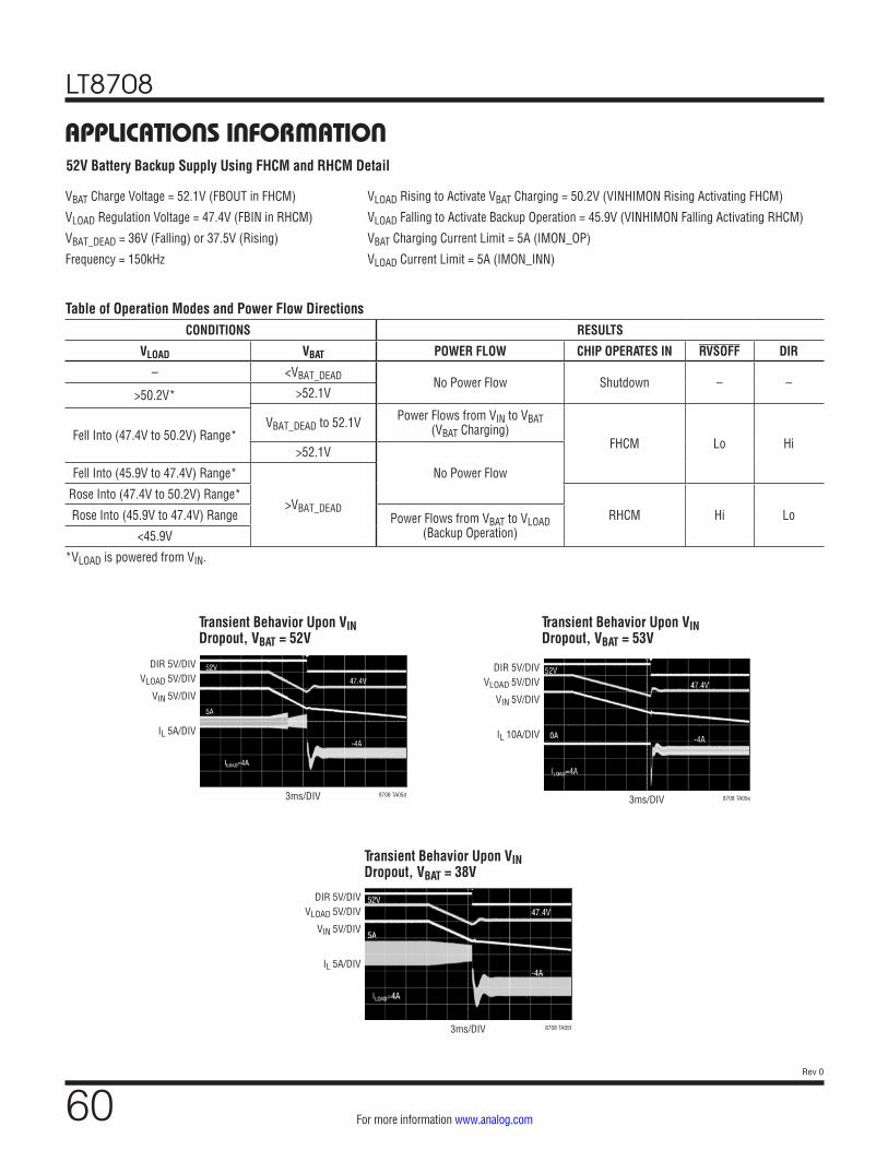
LT8708
60Rev 0
For more information www.analog.com
APPLICATIONS INFORMATION
Transient Behavior Upon VIN Dropout, VBAT = 52V
Transient Behavior Upon VIN Dropout, VBAT = 53V
Transient Behavior Upon VIN Dropout, VBAT = 38V
52V Battery Backup Supply Using FHCM and RHCM Detail
Table of Operation Modes and Power Flow DirectionsCONDITIONS RESULTS
VLOAD VBAT POWER FLOW CHIP OPERATES IN RVSOFF DIR
– <VBAT_DEAD No Power Flow Shutdown – –>50.2V* >52.1V
VBAT_DEAD to 52.1V Power Flows from VIN to VBAT (VBAT Charging)
FHCM Lo HiFell Into (47.4V to 50.2V) Range*
>52.1V
No Power FlowFell Into (45.9V to 47.4V) Range*
>VBAT_DEADRose Into (47.4V to 50.2V) Range*
RHCM Hi LoRose Into (45.9V to 47.4V) Range Power Flows from VBAT to VLOAD (Backup Operation)<45.9V
*VLOAD is powered from VIN.
VBAT Charge Voltage = 52.1V (FBOUT in FHCM) VLOAD Rising to Activate VBAT Charging = 50.2V (VINHIMON Rising Activating FHCM)
VLOAD Regulation Voltage = 47.4V (FBIN in RHCM) VLOAD Falling to Activate Backup Operation = 45.9V (VINHIMON Falling Activating RHCM)
VBAT_DEAD = 36V (Falling) or 37.5V (Rising) VBAT Charging Current Limit = 5A (IMON_OP)
Frequency = 150kHz VLOAD Current Limit = 5A (IMON_INN)
3ms/DIV 8708 TA05d
DIR 5V/DIVVLOAD 5V/DIV
VIN 5V/DIV
IL 5A/DIV
3ms/DIV 8708 TA05e
DIR 5V/DIVVLOAD 5V/DIV
VIN 5V/DIV
IL 10A/DIV
3ms/DIV 8708 TA05f
DIR 5V/DIVVLOAD 5V/DIV
VIN 5V/DIV
IL 5A/DIV
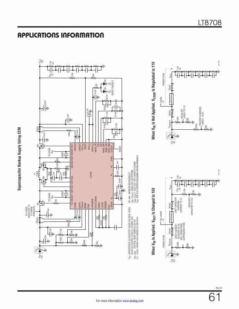
LT8708
61Rev 0
For more information www.analog.com
Supe
rcap
acito
r Bac
kup
Supp
ly U
sing
CCM
Whe
n V I
N Is
Not
App
lied,
VLO
AD Is
Reg
ulat
ed to
11V
Whe
n V I
N Is
App
lied,
VOU
T Is
Char
ged
to 1
5V
APPLICATIONS INFORMATION
10k
115k
REGU
LATE
CAPA
CITO
R TO
15V
LIM
IT C
APAC
ITOR
CHAR
GING
CU
RREN
T TO
1A
25m
Ω25
mΩ
POW
ER F
LOW
8708
TA0
6b
V IN
12V
D IN
12V
LOAD
S
29k
162k
V BAC
KUP IN
PUT
CURR
ENT
IN E
XCES
S OF
2A
WIL
L DR
AW F
ROM
SU
PERC
APAC
ITOR
S
V OUT
1.2k
×6C S
C ×6
CSPO
UT
CSNO
UTEX
TVCC
FBOU
T
INTV
CC
GATE
V CC
IMON
_OP
IMON
_INP
IMON
_ON
IMON
_INN
CLKO
UTSY
NCSS
RTV C
MOD
E
CSNI
NTG1
LT87
08
TG2
CSPI
NV I
NCHI
P
SHDN
FBIN
VINH
IMON
VOUT
LOM
ONSW
ENLD
O33
RVSO
FFDI
R
350k
HzICN
ICP
BOOS
T1SW
1BG
1CS
PCS
NGN
DBG
2SW
2BO
OST2
++
V IN
12V
C IN1
C IN2
D IN
LD03
3
C OUT
1
1.2k
×6
C OUT
2
C SC ×6
V OUT
15V
8708
TA0
6a
5.6n
F12
4k1µ
F22
0pF
15k
22nF
6.8n
F
17.4
k
22nF
26.7
k
6.8n
F
17.4
k
17.4
k
D B1
D B2
TOBO
OST1
TOBO
OST2
4Ω4.
7µF
10k
4.7µ
F
100Ω
1µF
47nF
115k
25m
Ω
TO D
IODE
DB1
TO D
IODE
D B
2
M4
0.22
µF
2Ω5m
Ω
10Ω
1nF
1nF
10Ω
0.22
µF
M3
M2
L12.
2μH
2Ω
M1
TO L
OADS
(R
EGUL
ATE
TO
11V
WHE
N IN
BAC
KUP)
25m
Ω
100Ω
1µF
4.7µ
F
71.5
k16
2k
20k
20k
20k
200k
150k
50k
50k
M1–
M4:
INF
INEO
N BS
C050
NE2L
SC I
N1, C
OUT2
: 22
0μF,
35V
35HV
P220
MC I
N2, C
OUT1
: 22
µF, 2
5V, T
DK C
4532
X741
E226
MC S
C: 6
0F, 2
.5V
COOP
ER B
USSM
AN H
B184
0-2R
5606
-R
D IN:
APP
ROPR
IATE
2A
SCHO
TTKY
DIO
DE O
R ID
EAL
DIOD
E
SUCH
AS
LTC4
358,
LTC
4412
, LTC
4352
, ETC
.D B
1, D
B2:
CENT
RAL
SEM
I CM
MR1
U-02
-LTE
L1:
2.2μ
H, V
ISHA
Y IH
LP-5
050C
E-01
-2R2
-M-0
1
25m
Ω25
mΩPO
WER
FLO
W
8708
TA0
6c
V IN 0V
D IN
LOAD
S
29k
200k
29k
162k
V BAC
KUP
V OUT
1.2k
×6RE
GULA
TELO
ADS
TO 1
1V
PREV
ENT
CHAR
GING
LOAD
S >
13.3
V

LT8708
62Rev 0
For more information www.analog.com
APPLICATIONS INFORMATION
Charging VOUT to 15V with 1A CurrentTransient Behavior Upon VIN Dropout (ILOAD = 4A)
Supercapacitor Backup Supply Using CCM Detail
VOUT Charge Voltage = 15V (FBOUT) VBACKUP Overvoltage Rising Threshold in Backup Operation = 13.3V (VINHIMON Rising)
VBACKUP Regulation Voltage = 11V (FBIN) VBACKUP Overvoltage Falling Threshold in Backup Operation = 12.9V (VINHIMON Falling)
VIN_MIN = 5.42V (Falling) or 5.65V (Rising) VOUT Charging Current Limit = 1A (IMON_OP)
Frequency = 350kHz VIN Current Limit = 2A (IMON_INP)
Table of Operation Modes and Power Flow DirectionsVBACKUP VOUT POWER FLOW CHIP OPERATES IN RVSOFF*
<VIN_MIN –NO POWER FLOW
Shutdown –
>13.3V>15V
CCM
Lo<15V Power Flows from VIN to VOUT (VOUT Charging)Fell Into (12.9V to 13.3V)
Range >15V No Power Flow
Rose Into (12.9V to 13.3V) Range <15V
Power Flows from VOUT to LOADS (Backup Operation)
HiPower Flows from VIN to VOUT
(VOUT Charging)>11V and <12.9V >15V
Power Flows from VOUT to LOADS (Backup Operation)<11V and >VIN_MIN –
*For use with LT8708-1(s)
20s/DIV 8708 TA06d
VIN5V/DIV
VOUT5V/DIV
IL5A/DIV
3s/DIV 8708 TA06e
VOUT5V/DIV
VBACKUP5V/DIV
IL5A/DIV
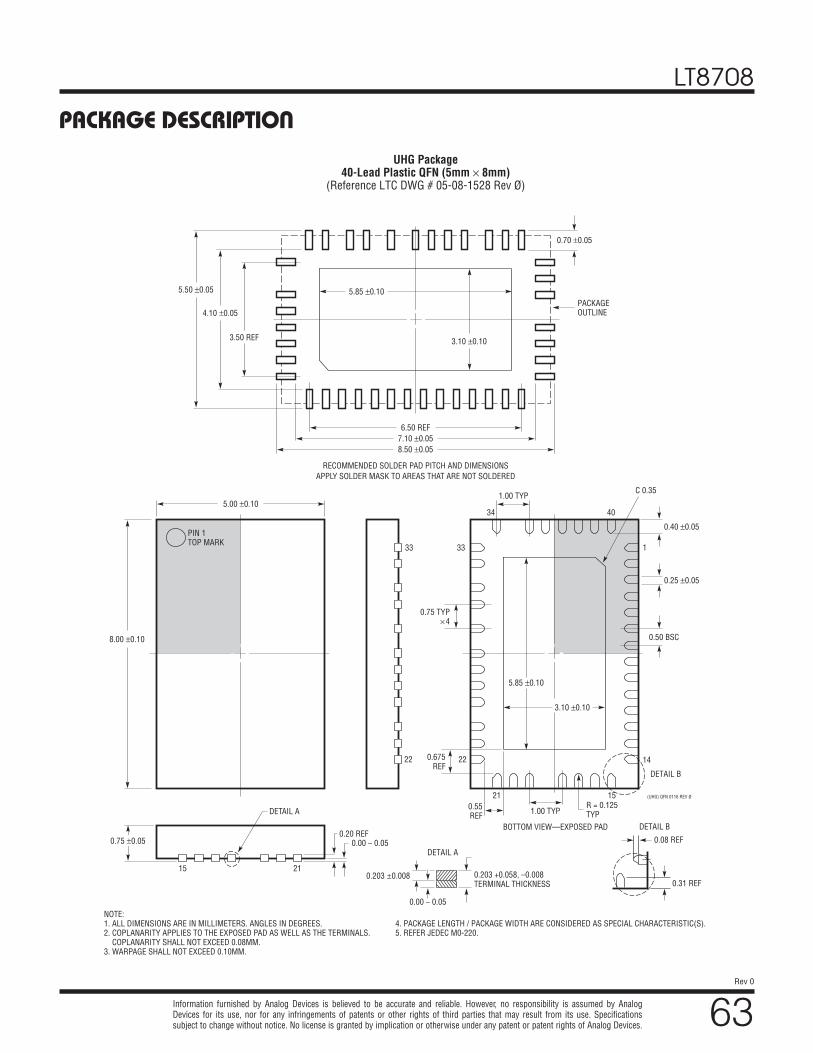
LT8708
63Rev 0
For more information www.analog.com
Information furnished by Analog Devices is believed to be accurate and reliable. However, no responsibility is assumed by Analog Devices for its use, nor for any infringements of patents or other rights of third parties that may result from its use. Specifications subject to change without notice. No license is granted by implication or otherwise under any patent or patent rights of Analog Devices.
PACKAGE DESCRIPTION
5.00 ±0.10
PIN 1TOP MARK
133
2222
33
14
21
2115
15
BOTTOM VIEW—EXPOSED PAD
3.10 ±0.10
0.675REF
0.55REF
5.85 ±0.10
0.75 TYP× 4
8.00 ±0.10
R = 0.125TYP
(UHG) QFN 0116 REV Ø
1.00 TYP
1.00 TYP
0.20 REF
DETAIL A
0.40 ±0.05
0.25 ±0.05
0.50 BSC
0.00 – 0.050.75 ±0.05
NOTE:1. ALL DIMENSIONS ARE IN MILLIMETERS. ANGLES IN DEGREES.2. COPLANARITY APPLIES TO THE EXPOSED PAD AS WELL AS THE TERMINALS. COPLANARITY SHALL NOT EXCEED 0.08MM.3. WARPAGE SHALL NOT EXCEED 0.10MM.
4. PACKAGE LENGTH / PACKAGE WIDTH ARE CONSIDERED AS SPECIAL CHARACTERISTIC(S).5. REFER JEDEC M0-220.
C 0.35
UHG Package40-Lead Plastic QFN (5mm × 8mm)
(Reference LTC DWG # 05-08-1528 Rev Ø)
4034
0.203 +0.058, –0.008TERMINAL THICKNESS
DETAIL A
0.00 – 0.05
0.203 ±0.008
DETAIL B
DETAIL B
0.08 REF
0.31 REF
3.10 ±0.10
5.85 ±0.10
0.70 ±0.05
6.50 REF
3.50 REF
4.10 ±0.05
5.50 ±0.05
7.10 ±0.058.50 ±0.05
PACKAGEOUTLINE
RECOMMENDED SOLDER PAD PITCH AND DIMENSIONSAPPLY SOLDER MASK TO AREAS THAT ARE NOT SOLDERED

LT8708
64Rev 0
For more information www.analog.com © ANALOG DEVICES, INC. 2018
D16897-0-6/18(0)www.analog.com
RELATED PARTS
TYPICAL APPLICATIONSupercapacitor Backup Supply Using CCM
CSPOUT
CSNOUTEXTVCCFBOUT
INTVCC
GATEVCCIMON_OP
IMON_INPIMON_ON
IMON_INNCLKOUTSYNCSSRTVCMODE
CSNINTG1
LT8708
TG2
CSPINVINCHIP
SHDNFBIN
VINHIMONVOUTLOMONSWENLDO33RVSOFFDIR
350kHz
ICNICP
BOOST1 SW1 BG1 CSP CSN GND BG2 SW2 BOOST2
++VIN12V
CIN1CIN2
DIN
LD033
COUT1
1.2k×6
COUT2
CSC×6
VOUT15V
8708 TA02
5.6nF124k 1µF
220pF
15k 22nF
6.8nF
17.4k
22nF26.7k
6.8nF
17.4k
17.4k
DB1 DB2
TOBOOST1
TOBOOST2
4Ω4.7µF10k
4.7µF
100Ω 1µF
4.7µF
115k
25mΩ
TO DIODE DB1
TO DIODE DB2
M4
0.22µF
2Ω5mΩ
10Ω
1nF
1nF10Ω0.22µF
M3M2
L12.2μH
2Ω
M1
TO LOADS (REGULATE TO
11V WHEN IN BACKUP)
25mΩ
100Ω
1µF
4.7µF
71.5k162k
20k20k
20k
200k
150k
50k
50k
M1–M4: INFINEON BSC050NE2LSCIN1, COUT2: 220μF, 35V 35HVP220MCIN2, COUT1: 22µF, 25V, TDK C4532X741E226MCSC: 60F, 2.5V COOPER BUSSMAN HB1840-2R5606-R
SEE MORE DETAILS OF THIS APPLICATION ON PAGE 61.DIN: APPROPRIATE 2A SCHOTTKY DIODE OR IDEAL DIODE SUCH AS LTC4358, LTC4412, LTC4352, ETC.DB1, DB2: CENTRAL SEMI CMMR1U-02-LTEL1: 2.2μH, VISHAY IHLP-5050CE-01-2R2-M-01
PART NUMBER DESCRIPTION COMMENTS
LT8708-1 80V Synchronous 4-Switch Buck-Boost DC/DC Slave Controller for LT8708 Multiphase System
2.8V (Need EXTVCC > 6.4V) ≤ VIN ≤ 80V,1.3V ≤ VOUT ≤ 80V, 5mm × 8mm QFN-40
LT8705A 80V VIN and VOUT Synchronous 4-Switch Buck-Boost DC/DC Controller
2.8V ≤ VIN ≤ 80V, Input and Output Current Monitor, 5mm × 7mm QFN-38 and TSSOP-38 Packages
LTC®3779 150V VIN and VOUT Synchronous 4-Switch Buck-Boost Controller
4.5V ≤ VIN ≤ 150V, 1.2V ≤ VOUT ≤ 150V, Up to 99% Efficiency Drives Logic-Level or STD Threshold MOSFETs, TSSOP-38 Package
LTC7813 60V Low IQ Synchronous Boost+Buck Controller Low EMI and Low Input/Output Ripple
4.5V (Down to 2.2V After Start-Up) ≤ VIN ≤ 60V, Boost VOUT Up to 60V, 0.8V ≤ Buck VOUT ≤ 60V, IQ = 29µA, 5mm × 5mm QFN-32 Package
LTC3899 60V, Triple Output, Buck/Buck/Boost Synchronous Controller with 29µA Burst Mode IQ
4.5V (Down to 2.2V after Start-Up) ≤ VIN ≤ 60V, VOUT Up to 60V, Buck VOUT Range: 0.8V to 60V, Boost VOUT Up to 60V
LTM®8056 58VIN, Buck-Boost µModule Regulator, Adjustable Input and Output Current Limiting
5V ≤ VIN ≤ 58V, 1.2V ≤ VOUT ≤ 48V, 15mm × 15mm × 4.92mm BGA Package
LTC3895/ LTC7801
150V Low IQ, Synchronous Step-Down DC/DC Controller with 100% Duty Cycle
4V ≤ VIN ≤ 140V, 150V ABS Max, PLL Fixed Frequency 50kHz to 900kHz, 0.8V ≤ VOUT ≤ 60V, Adjustable 5V to 10V Gate Drive, IQ = 40μA, 4mm × 5mm QFN-24, TSSOP-24, TSSOP-38(31) Packages
LTC3871 Bidirectional Multiphase DC/DC Synchronous Buck or Boost On-Demand Controller
VIN/VOUT Up to 100V, Ideal for High Power 48V/12V Automotive Battery Applications
LTC7103 105V, 2.3A, Low EMI Synchronous Step-Down Regulator
4.4V ≤ VIN ≤105V, 1V ≤ VOUT ≤ VIN, IQ = 2µA, Fixed Frequency 200kHz, 5mm × 6mm QFN Package