ltc1068-clock-tunable, quad second order, filter building ... · clock-tunable, quad second order,...
TRANSCRIPT
LTC1068 Series
11068fc
TYPICAL APPLICATION
DESCRIPTION
Clock-Tunable, Quad Second Order, Filter Building Blocks
The LTC®1068 product family consists of four monolithic clock-tunable filter building blocks. Each product contains four matched, low noise, high accuracy 2nd order switched-capacitor filter sections. An external clock tunes the center frequency of each 2nd order filter section. The LTC1068 products differ only in their clock-to-center frequency ratio. The clock-to-center frequency ratio is set to 200:1 (LTC1068-200), 100:1 (LTC1068), 50:1 (LTC1068-50) or 25:1 (LTC1068-25). External resistors can modify the clock-to-center frequency ratio. High performance, quad 2nd order, dual 4th order or 8th order filters can be designed with an LTC1068 family product. Designing filters with an LTC1068 product is fully supported by FilterCAD™ filter design software for Windows.
The LTC1068 products are available in a 28-pin SSOP surface mount package. A customized version of an LTC1068 family product can be obtained in a 16-lead SO package with internal thin-film resistors. Please contact LTC Marketing for details.
Gain vs Frequency
FEATURES
APPLICATIONS
n Four Identical 2nd Order Filter Sections in an SSOP Package
n 2nd Order Section Center Frequency Error: ±0.3% Typical and ±0.8% Maximumn Low Noise per 2nd Order Section, Q ≤ 5: LTC1068-200 50µVRMS, LTC1068 50µVRMS LTC1068-50 75µVRMS, LTC1068-25 90µVRMSn Low Power Supply Current: 4.5mA, Single 5V,
LTC1068-50n Operation with ±5V Power Supply, Single 5V
Supply or Single 3.3V Supply
n Lowpass or Highpass Filters: LTC1068-200, 0.5Hz to 25kHz; LTC1068, 1Hz to 50kHz; LTC1068-50, 2Hz to 50kHz; LTC1068-25, 4Hz to 200kHz
n Bandpass or Bandreject (Notch) Filters: LTC1068-200, 0.5Hz to 15kHz; LTC1068, 1Hz to 30kHz; LTC1068-50, 2Hz to 30kHz; LTC1068-25, 4Hz to 140kHz
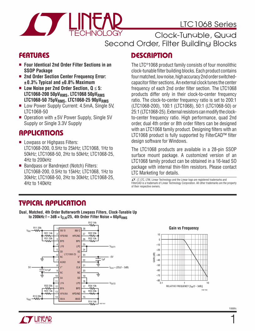
Dual, Matched, 4th Order Butterworth Lowpass Filters, Clock-Tunable Up to 200kHz f – 3dB = fCLK/25, 4th Order Filter Noise = 60µVRMS
INV B
HPB/NB
BPB
LPB
SB
NC
AGND
V+
NC
SA
LPA
BPA
HPA/NA
INVA
28
27
26
25
24
23
22
21
20
19
18
17
16
15
1
2
3
4
5
6
7
8
9
10
11
12
13
14
INV C
HPC/NC
BPC
LPC
SC
V–
NC
CLK
NC
SD
LPD
BPD
HPD/ND
INVD
LTC1068-25
R31 20k
R33 20k
R23 14k
R13 20k
0.1µF
R21 14k R22 20k
R12 14k
R32 10k
R34 10k
R24 20k
R14 14k
R11 20kVIN1
VIN2
5V
1µF
VOUT1
VOUT2
1068 TA01
–5V
fCLK = (25)(f – 3dB)
RELATIVE FREQUENCY [fIN/(f – 3dB)]0.1
GAIN
(dB)
–10
–20
–30
–40
–50
–60
–70
–801 10
1068 TA02
10
0
L, LT, LTC, LTM, Linear Technology and the Linear logo are registered trademarks and FilterCAD is a trademark of Linear Technology Corporation. All other trademarks are the property of their respective owners.

LTC1068 Series
21068fc
ABSOLUTE MAXIMUM RATINGSTotal Supply Voltage (V+ to V –) ................................12VPower Dissipation .............................................. 500mWInput Voltage at Any Pin ......V – – 0.3V ≤ VIN ≤ V+ + 0.3VStorage Temperature Range ................... –65°C to 150°C
(Note 1)
1
2
3
4
5
6
7
8
9
10
11
12
13
14
TOP VIEW
G PACKAGE28-LEAD PLASTIC SSOP
28
27
26
25
24
23
22
21
20
19
18
17
16
15
INV B
HPB/NB
BPB
LPB
SB
NC
AGND
V+
NC
SA
LPA
BPA
HPA/NA
INV A
INV C
HPC/NC
BPC
LPC
SC
V–
NC
CLK
NC
SD
LPD
BPD
HPD/ND
INV D
TJMAX = 110°C, θJA = 95°C/W
1
2
3
4
5
6
7
8
9
10
11
12
TOP VIEW
24
23
22
21
20
19
18
17
16
15
14
13
INV B
HPB/NB
BPB
LPB
SB
AGND
V+
SA
LPA
BPA
HPA/NA
INV A
INV C
HPC/NC
BPC
LPC
SC
V–
CLK
SD
LPD
BPD
HPD/ND
INV D
N PACKAGE24-LEAD PDIP
TJMAX = 110°C, θJA = 65°C/W
PIN CONFIGURATION
Operating Temperature Range LTC1068C ................................................ 0°C to 70°C LTC1068I............................................. –40°C to 85°CLead Temperature (Soldering, 10 sec) .................. 300°C
ORDER INFORMATIONLEAD FREE FINISH TAPE AND REEL PART MARKING PACKAGE DESCRIPTION TEMPERATURE RANGE
LTC1068CG#PBF LTC1068CG#TRPBF LTC1068 28-Lead Plastic SSOP 0°C to 70°C
LTC1068IG#PBF LTC1068IG#TRPBF LTC1068 28-Lead Plastic SSOP –40°C to 85°C
LTC1068-200CG#PBF LTC1068-200CG#TRPBF LTC1068 28-Lead Plastic SSOP 0°C to 70°C
LTC1068-200IG#PBF LTC1068-200IG#TRPBF LTC1068 28-Lead Plastic SSOP –40°C to 85°C
LTC1068-50CG#PBF LTC1068-50CG#TRPBF LTC1068 28-Lead Plastic SSOP 0°C to 70°C
LTC1068-50IG#PBF LTC1068-50IG#TRPBF LTC1068 28-Lead Plastic SSOP –40°C to 85°C
LTC1068-25CG#PBF LTC1068-25CG#TRPBF LTC1068 28-Lead Plastic SSOP 0°C to 70°C
LTC1068-25IG#PBF LTC1068-25IG#TRPBF LTC1068 28-Lead Plastic SSOP –40°C to 85°C
LTC1068CN#PBF NA LTC1068 24-Lead PDIP 0°C to 70°C
LTC1068IN#PBF NA LTC1068 24-Lead PDIP –40°C to 85°C
Consult LTC Marketing for parts specified with wider operating temperature ranges. Consult LTC Marketing for information on nonstandard lead based finish parts.For more information on lead free part marking, go to: http://www.linear.com/leadfree/ For more information on tape and reel specifications, go to: http://www.linear.com/tapeandreel/
LTC1068 Series
31068fc
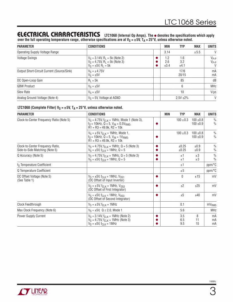
PARAMETER CONDITIONS MIN TYP MAX UNITS
Operating Supply Voltage Range 3.14 ±5.5 V
Voltage Swings VS = 3.14V, RL = 5k (Note 2) VS = 4.75V, RL = 5k (Note 3) VS = ±5V, RL = 5k
l
l
l
1.2 2.6
±3.4
1.6 3.2
±4.1
VP-P VP-P
V
Output Short-Circuit Current (Source/Sink) VS = ±4.75V VS = ±5V
17/6 20/15
mA mA
DC Open-Loop Gain RL = 5k 85 dB
GBW Product VS = ±5V 6 MHz
Slew Rate VS = ±5V 10 V/µs
Analog Ground Voltage (Note 4) VS = 5V, Voltage at AGND 2.5V ±2% V
PARAMETER CONDITIONS MIN TYP MAX UNITS
Clock-to-Center Frequency Ratio (Note 5) VS = 4.75V, fCLK = 1MHz, Mode 1 (Note 3), fO = 10kHz, Q = 5, VIN = 0.5VRMS, R1 = R3 = 49.9k, R2 = 10k
l
100 ±0.3 100 ±0.8 100 ±0.9
% %
VS = ±5V, fCLK = 1MHz, Mode 1, fO = 10kHz, Q = 5, VIN = 1VRMS, R1 = R3 = 49.9k, R2 = 10k
l
100 ±0.3 100 ±0.8 100 ±0.9
% %
Clock-to-Center Frequency Ratio, Side-to-Side Matching (Note 5)
VS = 4.75V, fCLK = 1MHz, Q = 5 (Note 3) VS = ±5V, fCLK = 1MHz, Q = 5
l
l
±0.25 ±0.25
±0.9 ±0.9
% %
Q Accuracy (Note 5) VS = 4.75V, fCLK = 1MHz, Q = 5 (Note 3) VS = ±5V, fCLK = 1MHz, Q = 5
l
l
±1 ±1
±3 ±3
% %
fO Temperature Coefficient ±1 ppm/°C
Q Temperature Coefficient ±5 ppm/°C
DC Offset Voltage (Note 5) (See Table 1)
VS = ±5V, fCLK = 1MHz, VOS1 (DC Offset of Input Inverter)
l 0 ±15 mV
VS = ±5V, fCLK = 1MHz, VOS2 (DC Offset of First Integrator)
l ±2 ±25 mV
VS = ±5V, fCLK = 1MHz, VOS3 (DC Offset of Second Integrator)
l ±5 ±40 mV
Clock Feedthrough VS = ±5V, fCLK = 1MHz 0.1 mVRMS
Max Clock Frequency (Note 6) VS = ±5V, Q ≤ 2.0, Mode 1 5.6 MHz
Power Supply Current VS = 3.14V, fCLK = 1MHz (Note 2) VS = 4.75V, fCLK = 1MHz (Note 3) VS = ±5V, fCLK = 1MHz
l
l
l
3.5 6.5 9.5
8 11 15
mA mA mA
ELECTRICAL CHARACTERISTICS LTC1068 (Internal Op Amps). The l denotes the specifications which apply over the full operating temperature range, otherwise specifications are at VS = ±5V, TA = 25°V, unless otherwise noted.
LTC1068 (Complete Filter) VS = ±5V, TA = 25°V, unless otherwise noted.

LTC1068 Series
41068fc
ELECTRICAL CHARACTERISTICS LTC1068-200 (Internal Op Amps). The l denotes the specifications which apply over the full operating temperature range, otherwise specifications are at VS = ±5V, TA = 25°V, unless otherwise noted.
PARAMETER CONDITIONS MIN TYP MAX UNITS
Operating Supply Voltage Range 3.14 ±5.5 V
Voltage Swings VS = 3.14V, RL = 5k (Note 2) VS = 4.75V, RL = 5k (Note 3) VS = ±5V, RL = 5k
l
l
l
1.2 2.6
±3.4
1.6 3.2
±4.1
VP-P VP-P
V
Output Short-Circuit Current (Source/Sink) VS = ±4.75V VS = ±5V
17/6 20/15
mA mA
DC Open-Loop Gain RL = 5k 85 dB
GBW Product VS = ±5V 6 MHz
Slew Rate VS = ±5V 10 V/µs
Analog Ground Voltage (Note 4) VS = 5V, Voltage at AGND 2.5V ±2% V
LTC1068-200 (Complete Filter) VS = ±5V, TA = 25°V, unless otherwise noted.
PARAMETER CONDITIONS MIN TYP MAX UNITS
Clock-to-Center Frequency Ratio (Note 5) VS = 4.75V, fCLK = 1MHz, Mode 1 (Note 3), fO = 5kHz, Q = 5, VIN = 0.5VRMS, R1 = R3 = 49.9k, R2 = 10k
l
200 ±0.3 200 ±0.8 200 ±0.9
% %
VS = ±5V, fCLK = 1MHz, Mode 1, fO = 5Hz, Q = 5, VIN = 1VRMS, R1 = R3 = 49.9k, R2 = 10k
l
200 ±0.3 200 ±0.8 200 ±0.9
% %
Clock-to-Center Frequency Ratio, Side-to-Side Matching (Note 5)
VS = 4.75V, fCLK = 1MHz, Q = 5 (Note 3) VS = ±5V, fCLK = 1MHz, Q = 5
l
l
±0.25 ±0.25
±0.9 ±0.9
% %
Q Accuracy (Note 5) VS = 4.75V, fCLK = 1MHz, Q = 5 (Note 3) VS = ±5V, fCLK = 1MHz, Q = 5
l
l
±1 ±1
±3 ±3
% %
fO Temperature Coefficient ±1 ppm/°C
Q Temperature Coefficient ±5 ppm/°C
DC Offset Voltage (Note 5) (See Table 1)
VS = ±5V, fCLK = 1MHz, VOS1 (DC Offset of Input Inverter)
l 0 ±15 mV
VS = ±5V, fCLK = 1MHz, VOS2 (DC Offset of First Integrator)
l ±2 ±25 mV
VS = ±5V, fCLK = 1MHz, VOS3 (DC Offset of Second Integrator)
l ±5 ±40 mV
Clock Feedthrough VS = ±5V, fCLK = 1MHz 0.1 mVRMS
Max Clock Frequency (Note 6) VS = ±5V, Q ≤ 2.0, Mode 1 5.6 MHz
Power Supply Current VS = 3.14V, fCLK = 1MHz (Note 2) VS = 4.75V, fCLK = 1MHz (Note 3) VS = ±5V, fCLK = 1MHz
l
l
l
3.5 6.5 9.5
8 11 15
mA mA mA

LTC1068 Series
51068fc
ELECTRICAL CHARACTERISTICS LTC1068-50 (Internal Op Amps). The l denotes the specifications which apply over the full operating temperature range, otherwise specifications are at VS = ±5V, TA = 25°V, unless otherwise noted.
PARAMETER CONDITIONS MIN TYP MAX UNITS
Operating Supply Voltage Range 3.14 ±5.5 V
Voltage Swings VS = 3.14V, RL = 5k (Note 2) VS = 4.75V, RL = 5k (Note 3) VS = ±5V, RL = 5k
l
l
l
1.2 2.6
±3.4
1.8 3.6
±4.1
VP-P VP-P
V
Output Short-Circuit Current (Source/Sink) VS = ±3.14V VS = ±5V
17/6 20/15
mA mA
DC Open-Loop Gain RL = 5k 85 dB
GBW Product VS = ±5V 4 MHz
Slew Rate VS = ±5V 7 V/µs
Analog Ground Voltage (Note 4) VS = 5V, Voltage at AGND 2.175V ±2% V
LTC1068-50 (Complete Filter) VS = ±5V, TA = 25°V, unless otherwise noted.
PARAMETER CONDITIONS MIN TYP MAX UNITS
Clock-to-Center Frequency Ratio (Note 5) VS = 3.14V, fCLK = 250kHz, Mode 1 (Note 2), fO = 5kHz, Q = 5, VIN = 0.34VRMS, R1 = R3 = 49.9k, R2 = 10k
l
50 ±0.3 50 ±0.8 50 ±0.9
% %
VS = ±5V, fCLK = 500kHz, Mode 1, fO = 10kHz, Q = 5, VIN = 1VRMS, R1 = R3 = 49.9k, R2 = 10k
l
50 ±0.3 50 ±0.8 50 ±0.9
% %
Clock-to-Center Frequency Ratio, Side-to-Side Matching (Note 5)
VS = 3.14V, fCLK = 250kHz, Q = 5 (Note 2) VS = ±5V, fCLK = 500kHz, Q = 5
l
l
±0.25 ±0.25
±0.9 ±0.9
% %
Q Accuracy (Note 5) VS = 3.14V, fCLK = 250kHz, Q = 5 (Note 2) VS = ±5V, fCLK = 500kHz, Q = 5
l
l
±1 ±1
±3 ±3
% %
fO Temperature Coefficient ±1 ppm/°C
Q Temperature Coefficient ±5 ppm/°C
DC Offset Voltage (Note 5) (See Table 1)
VS = ±5V, fCLK = 500kHz, VOS1 (DC Offset of Input Inverter)
l 0 ±15 mV
VS = ±5V, fCLK = 500kHz, VOS2 (DC Offset of First Integrator)
l –2 ±25 mV
VS = ±5V, fCLK = 500kHz, VOS3 (DC Offset of Second Integrator)
l –5 ±40 mV
Clock Feedthrough VS = ±5V, fCLK = 500kHz 0.16 mVRMS
Max Clock Frequency (Note 6) VS = ±5V, Q ≤ 1.6, Mode 1 3.4 MHz
Power Supply Current VS = 3.14V, fCLK = 250kHz (Note 2) VS = 4.75V, fCLK = 250kHz (Note 3) VS = ±5V, fCLK = 500kHz
l
l
l
3.0 4.3 6.0
5 8
11
mA mA mA

LTC1068 Series
61068fc
ELECTRICAL CHARACTERISTICS LTC1068-25 (Internal Op Amps). The l denotes the specifications which apply over the full operating temperature range, otherwise specifications are at VS = ±5V, TA = 25°V, unless otherwise noted.
PARAMETER CONDITIONS MIN TYP MAX UNITS
Operating Supply Voltage Range 3.14 ±5.5 V
Voltage Swings VS = 3.14V, RL = 5k (Note 2) VS = 4.75V, RL = 5k (Note 3) VS = ±5V, RL = 5k
l
l
l
1.2 2.6
±3.4
1.6 3.4
±4.1
VP-P VP-P
V
Output Short-Circuit Current (Source/Sink) VS = ±4.75V VS = ±5V
17/6 20/15
mA mA
DC Open-Loop Gain RL = 5k 85 dB
GBW Product VS = ±5V 6 MHz
Slew Rate VS = ±5V 10 V/µs
Analog Ground Voltage (Note 4) VS = 5V, Voltage at AGND 2.5V ±2% V
LTC1068-25 (Complete Filter) VS = ±5V, TA = 25°V, unless otherwise noted.
PARAMETER CONDITIONS MIN TYP MAX UNITS
Clock-to-Center Frequency Ratio (Note 5) VS = 4.75V, fCLK = 500kHz, Mode 1 (Note 3), fO = 20kHz, Q = 5, VIN = 0.5VRMS, R1 = R3 = 49.9k, R2 = 10k
l
25 ±0.3 25 ±0.8 25 ±0.9
% %
VS = ±5V, fCLK = 1MHz, Mode 1, fO = 40kHz, Q = 5, VIN = 1VRMS, R1 = R3 = 49.9k, R2 = 10k
l
25 ±0.3 25 ±0.8 25 ±0.9
% %
Clock-to-Center Frequency Ratio, Side-to-Side Matching (Note 5)
VS = 4.75V, fCLK = 500kHz, Q = 5 (Note 3) VS = ±5V, fCLK = 1MHz, Q = 5
l
l
±0.25 ±0.25
±0.9 ±0.9
% %
Q Accuracy (Note 5) VS = 4.75V, fCLK = 500kHz, Q = 5 (Note 3) VS = ±5V, fCLK = 1MHz, Q = 5
l
l
±1 ±1
±3 ±3
% %
fO Temperature Coefficient ±1 ppm/°C
Q Temperature Coefficient ±5 ppm/°C
DC Offset Voltage (Note 5) (See Table 1)
VS = ±5V, fCLK = 1MHz, VOS1 (DC Offset of Input Inverter)
l 0 ±15 mV
VS = ±5V, fCLK = 1MHz, VOS2 (DC Offset of First Integrator)
l –2 ±25 mV
VS = ±5V, fCLK = 1MHz, VOS3 (DC Offset of Second Integrator)
l –5 ±40 mV
Clock Feedthrough VS = ±5V, fCLK = 1MHz 0.25 mVRMS
Max Clock Frequency (Note 6) VS = ±5V, Q ≤ 1.6, Mode 1 5.6 MHz
Power Supply Current VS = 3.14V, fCLK = 1MHz (Note 2) VS = 4.75V, fCLK = 1MHz (Note 3) VS = ±5V, fCLK = 1MHz
l
l
l
3.5 6.5 9.5
8 11 15
mA mA mA
Note 1: Stresses beyond those listed under Absolute Maximum Ratings may cause permanent damage to the device. Exposure to any Absolute Maximum Rating condition for extended periods may affect device reliability and lifetime.Note 2: Production testing for single 3.14V supply is achieved by using the equivalent dual supplies of ±1.57V.Note 3: Production testing for single 4.75V supply is achieved by using the equivalent dual supplies of ±2.375V.
Note 4: Pin 7 (AGND) is the internal analog ground of the device. For single supply applications this pin should be bypassed with a 1µF capacitor. The biasing voltage of AGND is set with an internal resistive divider from Pin 8 to Pin 23 (see Block Diagram).Note 5: Side D is guaranteed by design.Note 6: See Typical Performance Characteristics.

LTC1068 Series
71068fc
ELECTRICAL CHARACTERISTICS
LTC1068Maximum Q vs Center Frequency (Modes 1, 1b, 2)
LTC1068Maximum Q vs Center Frequency (Modes 2, 3)
LTC1068-200Maximum Q vs Center Frequency(Modes 1, 1b, 2)
Table 1. Output DC Offsets One 2nd Order SectionMODE VOSN VOSBP VOSLP
1 VOS1[(1/Q) + 1 + ||HOLP||] – VOS3/Q VOS3 VOSN – VOS2
1b VOS1[(1/Q) + 1 + R2/R1] – VOS3/Q VOS3 ~(VOSN – VOS2)(1 + R5/R6)
2 [VOS1(1 + R2/R1 + R2/R3 + R2/R4) – VOS3(R2/R3)X [R4/(R2 + R4)] + VOS2[R2/(R2 + R4)]
VOS3 VOSN – VOS2
3 VOS2 VOS3 VOS1[1 + R4/R1 + R4/R2 + R4/R3] – VOS2(R4/R2) – VOS3(R4/R3)
TYPICAL PERFORMANCE CHARACTERISTICS
CENTER FREQUENCY, fO (kHz)0
A B C0
MAX
IMUM
Q
5
15
20
25
50
35
20 40 50
1068 G01
10
40
45
30
10 30 60 70
A. VS = 3.3V, fCLK(MAX) = 1.5MHzB. VS = 5V, fCLK(MAX) = 3.4MHzC. VS = ±5V, fCLK(MAX) = 5.6MHz(FOR MODE 2 R4 ≥ 10R2)
CENTER FREQUENCY, fO (kHz)0
A B C0
MAX
IMUM
Q
5
15
20
25
50
35
20 40 50
1068 G02
10
40
45
30
10 30 60
A. VS = 3.3V, fCLK(MAX) = 1MHzB. VS = 5V, fCLK(MAX) = 3MHzC. VS = ±5V, fCLK(MAX) = 5MHz(FOR MODE 2 R4 < 10R2)
CENTER FREQUENCY, fO (kHz)0
A B C
55
50
45
40
35
30
25
20
15
10
5
0
TYP
ICAL
MAX
IMUM
Q
8 16 20 24
1068 G03
4 12 28 32
A: VS = 3.3V, fCLK(MAX) = 1.2MHzB: VS = 5V, fCLK(MAX) = 3.2MHzC: VS = ±5V, fCLK(MAX) = 6.1MHz
(FOR MODE 2, R4 ≥ 10R2)
LTC1068-200Maximum Q vs Center Frequency(Modes 2, 3)
LTC1068-50Maximum Q vs Center Frequency (Modes 1, 1b, 2)
LTC1068-50Maximum Q vs Center Frequency(Modes 2, 3)
CENTER FREQUENCY, fO (kHz)0
A B C
55
50
45
40
35
30
25
20
15
10
5
0
TYP
ICAL
MAX
IMUM
Q
8 16 20 24
1068 G04
4 12 28 32
A: VS = 3.3V, fCLK(MAX) = 1.2MHzB: VS = 5V, fCLK(MAX) = 3.2MHzC: VS = ±5V, fCLK(MAX) = 6.1MHz
(FOR MODE 2, R4 < 10R2)
CENTER FREQUENCY, fO (kHz)0
A
B C
55
50
45
40
35
30
25
20
15
10
5
0
TYP
ICAL
MAX
IMUM
Q
8 16 20 24
1068 G05
4 12 28 32
A: VS = 3.3V, fCLK(MAX) = 1.1MHzB: VS = 5V, fCLK(MAX) = 2.1MHzC: VS = ±5V, fCLK(MAX) = 3.6MHz
(FOR MODE 2, R4 ≥ 10R2)
CENTER FREQUENCY, fO (kHz)0
A
BC
55
50
45
40
35
30
25
20
15
10
5
0
TYP
ICAL
MAX
IMUM
Q
8 16 20 24
1068 G06
4 12 28 32
A: VS = 3.3V, fCLK(MAX) = 1.1MHzB: VS = 5V, fCLK(MAX) = 2.1MHzC: VS = ±5V, fCLK(MAX) = 3.6MHz
(FOR MODE 2, R4 < 10R2)

LTC1068 Series
81068fc
TYPICAL PERFORMANCE CHARACTERISTICS
LTC1068-25Maximum Q vs Center Frequency(Modes 1, 1b, 2)
LTC1068-25Maximum Q vs Center Frequency (Modes 2, 3)
LTC1068 Center Frequency Variation vs Clock Frequency
LTC1068-200 Center Frequency Variation vs Clock Frequency
LTC1068-50 Center Frequency Variation vs Clock Frequency
LTC1068-25 Center Frequency Variation vs Clock Frequency
CENTER FREQUENCY, fO (kHz)0
A B C
TYP
ICAL
MAX
IMUM
Q
55
50
45
40
35
30
25
20
15
10
5
064 128 160
1068 G07
32 96 192 224
A: VS = 3.3V, fCLK(MAX) = 1.2MHzB: VS = 5V, fCLK(MAX) = 3.4MHzC: VS = ±5V, fCLK(MAX) = 6.1MHz(FOR MODE 2, R4 ≥ 10R2)
FREQUENCY, fO (kHz)0
A B C
TYP
ICAL
MAX
IMUM
Q
55
50
45
40
35
30
25
20
15
10
5
064 128 160
1068 G08
32 96 192 224
A: VS = 3.3V, fCLK(MAX) = 1MHzB: VS = 5V, fCLK(MAX) = 3MHzC: VS = ±5V, fCLK(MAX) = 5MHz(FOR MODE 2, R4 < 10R2)
CLOCK FREQUENCY (MHz)0.75 1.25 1.75 2.25 2.75 3.25 3.75
–0.6CENT
ER F
REQU
ENCY
VAR
IATI
ON (%
ERR
OR)
–0.4
0
0.2
0.4
1.2
1068 G09
–0.2
4.25
0.6
0.8
1.0
MODE 3
MODE 1
VS = ±5VQ = 5, REFERENCECENTER FREQUENCY WITH fCLK = 0.75MHz
CLOCK FREQUENCY (MHz)0.75 1.25 1.75 2.25 2.75 3.25 3.75
–0.25CENT
ER F
REQU
ENCY
VAR
IATI
ON (%
ERR
OR)
–0.20
–0.10
–0.05
0
0.20
1068 G10
–0.15
4.25
0.05
0.10
0.15
MODE 3
MODE 1
VS = ±5VQ = 5, REFERENCECENTER FREQUENCY WITH fCLK = 0.75MHz
CLOCK FREQUENCY (MHz)0.5
–0.2
CENT
ER F
REQU
ENCY
VAR
IATI
ON (%
ERR
OR)
–0.1
0
0.1
0.2
0.4
0.75 1.0 1.25 1.5
1068 G11
1.75 2.0
0.3MODE 1
MODE 3
VS = ±5VQ = 5, REFERENCECENTER FREQUENCY WITH fCLK = 0.5MHz
CLOCK FREQUENCY (MHz)0.5
0
BATT
ERY
VOLT
AGE
(V)
0.3
0.8
1.3
1.8
1.0 1.5 2.0 2.5
1068 G12
3.0 3.5
MODE 1
MODE 3
VS = ±5VQ = 5, REFERENCECENTER FREQUENCY WITH fCLK = 0.5MHz
LTC1068/LTC1068-200Noise vs Q
LTC1068-50 Noise vs Q
LTC1068-25 Noise vs Q
Q0
0
NOIS
E (µ
V RM
S)
50
100
150
200
10 20 30
5V ±5V
3.3V
40
1068 G13
250
300
5 15 25 35Q
00
NOIS
E (µ
V RM
S)
50
100
150
200
10 20 30
±5V
3.3V
40
1068 G14
250
300
5 15 25 35
5V
Q0
0
NOIS
E (µ
V RM
S)
50
100
150
200
10 20 30
±5V
3.3V
40
1068 G15
250
300
5 15 25 35
5V
LTC1068 Series
91068fc
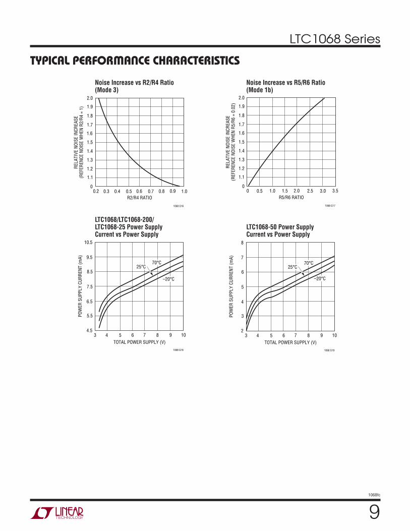
TYPICAL PERFORMANCE CHARACTERISTICS
Noise Increase vs R2/R4 Ratio(Mode 3)
Noise Increase vs R5/R6 Ratio(Mode 1b)
LTC1068/LTC1068-200/ LTC1068-25 Power Supply Current vs Power Supply
LTC1068-50 Power Supply Current vs Power Supply
R2/R4 RATIO0.2
0
RELA
TIVE
NOI
SE IN
CREA
SE(R
EFER
ENCE
NOI
SE W
HEN
R2/R
4 =
1)
1.1
1.3
1.4
1.5
2.0
1.7
0.4 0.6 0.7
1068 G16
1.2
1.8
1.9
1.6
0.3 0.5 0.8 0.9 1.0R5/R6 RATIO
00
RELA
TIVE
NOI
SE IN
CREA
SE(R
EFER
ENCE
NOI
SE W
HEN
R5/R
6 =
0.02
)
1.1
1.3
1.4
1.5
2.0
1.7
1.0 2.0 2.5
1068 G17
1.2
1.8
1.9
1.6
0.5 1.5 3.0 3.5
TOTAL POWER SUPPLY (V)3
POW
ER S
UPPL
Y CU
RREN
T (m
A)
8.5
9.5
10.5
6 8
1068 G18
7.5
6.5
4 5 7 9 10
5.5
4.5
25°C70°C
–20°C
TOTAL POWER SUPPLY (V)3
POW
ER S
UPPL
Y CU
RREN
T (m
A)
6
7
8
6 8
1068 G19
5
4
4 5 7 9 10
3
2
25°C70°C
–20°C

LTC1068 Series
101068fc
PIN FUNCTIONSPower Supply Pins
The V + and V– pins should each be bypassed with a 0.1µF capacitor to an adequate analog ground. The filter’s power supplies should be isolated from other digital or high voltage analog supplies. A low noise linear supply is recommended. Using a switching power supply will lower the signal-to-noise ratio of the filter. Figures 1 and 2 show typical connections for dual and single supply operation.
Analog Ground Pin
The filter’s performance depends on the quality of the analog signal ground. For either dual or single supply operation, an analog ground plane surrounding the package is recom-mended. The analog ground plane should be connected to any digital ground at a single point. For single supply operation, AGND should be bypassed to the analog ground plane with at least a 0.47µF capacitor (Figure 2).
Two internal resistors bias the analog ground pin. For the LTC1068, LTC1068-200 and LTC1068-25, the voltage at the analog ground pin (AGND) for single supply is 0.5 × V+ and for the LTC1068-50 it is 0.435 × V+.
Clock Input Pin
Any TTL or CMOS clock source with a square-wave output and 50% duty cycle (±10%) is an adequate clock source for the device. The power supply for the clock source should not be the filter’s power supply. The analog ground for the filter should be connected to clock’s ground at a single point only. Table 2 shows the clock’s low and high level threshold values for dual or single supply operation.
Table 2. Clock Source High and Low Threshold LevelsPOWER SUPPLY HIGH LEVEL LOW LEVEL
Dual Supply = ±5V ≥ 1.53V ≤ 0.53V
Single Supply = 5V ≥ 1.53V ≤ 0.53V
Single Supply = 3.3V ≥ 1.20V ≤ 0.53V
A pulsed generator can be used as a clock source provided the high level ON time is at least 25% of the pulse period. Sine waves are not recommended for clock input frequen-cies less than 100kHz, since excessively slow clock rise or fall times generate internal clock jitter (maximum clock rise or fall time ≤ 1µs). The clock signal should be routed from the right side of the IC package and perpendicular to it to avoid coupling to any input or output analog signal
Figure 1. Dual Supply Ground Plane Connections Figure 2. Single Supply Ground Plane Connections
0.1µFV–
1068 F01
200Ω
DIGITAL GROUND
V+LTC1068
CLOCKSOURCE
0.1µF
ANALOGGROUNDPLANE
28
27
26
25
24
23
22
21
20
19
18
17
16
15
1
2
3
4
5
6
7
8
9
10
11
12
13
14
STARSYSTEMGROUND
1068 F02
200Ω
DIGITAL GROUNDFOR MODE 3, THE S NODE SHOULD BE TIED TO PIN 7 (AGND)
V+
LTC1068
RA RB
CLOCKSOURCE
0.1µF
VAGND
0.47µF(1µF FOR STOPBANDFREQUENCIES≤1kHz)
ANALOGGROUNDPLANE
28
27
26
25
24
23
22
21
20
19
18
17
16
15
1
2
3
4
5
6
7
8
9
10
11
12
13
14
STARSYSTEMGROUND
DEVICELTC1068LTC1068-200LTC1068-25LTC1068-50
RA
10k
11.3k
RB
10k
8.6k

LTC1068 Series
111068fc
PIN FUNCTIONS
BLOCK DIAGRAM
path. A 200Ω resistor between clock source and Pin 11 will slow down the rise and fall times of the clock to further reduce charge coupling (Figures 1 and 2).
Output Pins
Each 2nd order section of an LTC1068 device has three outputs that typically source 17mA and sink 6mA. Driv-ing coaxial cables or resistive loads less than 20k will degrade the total harmonic distortion performance of any filter design. When evaluating the distortion or noise performance of a particular filter design implemented with a LTC1068 device, the final output of the filter should be buffered with a wideband, noninverting high slew rate amplifier (Figure 3).
Inverting Input Pins
These pins are the inverting inputs of internal op amps and are susceptible to stray capacitive coupling from low impedance signal outputs and power supply lines.
In a printed circuit layout any signal trace, clock source trace or power supply trace should be at least 0.1 inches away from any inverting input pins
Summing Input Pins
These are voltage input pins. If used, they should be driven with a source impedance below 5k. When they are not used, they should be tied to the analog ground pin.
The summing pin connections determine the circuit to-pology (mode) of each 2nd order section. Please refer to Modes of Operation.
Figure 3. Wideband Buffer
+
–LT®1354
1k
1068 F03
+ +
RA*
RB*
V+ (8)
CLK (21)
V– (23)
NC (6)
NC (9)
NC (20)
NC (22)
AGND (7)
1068 BD
–
++ +
+
+
+
+
+
HPC/NC(27)
BPC(26)
LPC(25)
HPB/NB(2)
BPB(3)
LPB(4)
*THE RATIO RA/RB VARIES ±2%
BPA(12)
LPA(11)
INV A(14)
AGND(7)
INV C(28)
HPA/NA(13)
+ Σ
SA(10)
–
+–
+
–
+
–
+
INV D(15)
INV B(1)
HPD/ND(16)
Σ–
SB(5)
Σ–
SC(24)
Σ–
SD(19)
+
+
BPD(17)
LPD(18)
PIN 28-LEAD SSOP PACKAGE
DEVICELTC1068LTC1068-200LTC1068-25LTC1068-50
RA
10k
11.3k
RB
10k
8.6k
LTC1068 Series
121068fc
MODES OF OPERATIONLinear Technology’s universal switched-capacitor filters are designed for a fixed internal, nominal fCLK/fO ratio. The fCLK/fO ratio is 100 for the LTC1068, 200 for the LTC1068-200, 50 for the LTC1068-50 and 25 for the LTC1068-25. Filter designs often require the fCLK/fO ratio of each section to be different from the nominal ratio and in most cases different from each other. Ratios other than the nominal value are possible with external resistors. Operating modes use external resistors, connected in different arrangements to realize different fCLK/fO ratios. By choosing the proper mode, the fCLK/fO ratio can be increased or decreased from the part’s nominal ratio.
The choice of operating mode also effects the transfer function at the HP/N pins. The LP and BP pins always give the lowpass and bandpass transfer functions respectively, regardless of the mode utilized. The HP/N pins have a different transfer function depending on the mode used. Mode 1 yields a notch transfer function. Mode 3 yields a highpass transfer function. Mode 2 yields a highpass notch transfer function (i.e., a highpass with a stopband notch). More complex transfer functions, such as lowpass notch, allpass or complex zeros, are achieved by summing two or more of the LP, BP or HP/N outputs. This is illustrated in sections Mode 2n and Mode 3a.
Choosing the proper mode(s) for a particular application is not trivial and involves much more than just adjusting the fCLK/fO ratio. Listed here are four of the nearly twenty modes available. To make the design process simpler and quicker, Linear Technology has developed the FilterCAD for Widows design software. FilterCAD is an easy-to-use, powerful and interactive filter design program. The de-signer can enter a few filter specifications and the program produces a full schematic. FilterCAD allows the designer to concentrate on the filter’s transfer function and not get bogged down in the details of the design. Alternatively, those who have experience with the Linear Technology family of parts can control all of the details themselves. For a complete listing of all the operating modes, consult the appendices of the FilterCAD manual or the Help files in FilterCAD. FilterCAD can be obtained free of charge on the Linear Technology web site (www.linear.com) or you can order the FilterCAD CD-ROM by contacting Linear Technology Marketing.
Mode 1
In Mode 1, the ratio of the external clock frequency to the center frequency of each 2nd order section is inter-nally fixed at the part’s nominal ratio. Figure 4 illustrates Mode 1 providing 2nd order notch, lowpass and band-pass outputs. Mode 1 can be used to make high order Butterworth lowpass filters; it can also be used to make low Q notches and for cascading 2nd order bandpass functions tuned at the same center frequency. Mode 1 is faster than Mode 3.
Please refer to the Operating Limits paragraph under Applica-tions Information for a guide to the use of capacitor CC.
Mode 1b
Mode 1b is derived from Mode 1. In Mode 1b (Figure 5) two additional resistors R5 and R6 are added to lower the amount of voltage fed back from the lowpass output into the input of the SA (or SB) switched-capacitor summer. This allows the filter’s clock-to-center frequency ratio to be adjusted beyond the part’s nominal ratio. Mode 1b maintains the speed advantages of Mode 1 and should be considered an optimum mode for high Q designs with fCLK to fCUTOFF (or fCENTER) ratios greater than the part’s nominal ratio.
The parallel combination of R5 and R6 should be kept below 5k.
Please refer to the Operating Limits paragraph under Applica-tions Information for a guide to the use of capacitor CC.
Figure 4. Mode 1, 2nd Order Filter Providing Notch, Bandpassing and Lowpass Outputs
–
+Σ
AGND
R1
N BP LP
VIN
1068 F04
+ –
SR2
R3
CC
fO = ; fn = fO
Q = ; HON = – ; HOBP = –
HOLP = HON
R2R1
R3R1
R3R2
fCLKRATIO
DEVICELTC1068LTC1068-200LTC1068-50LTC1068-25
RATIO1002005025

LTC1068 Series
131068fc
MODES OF OPERATION
Mode 3
In Mode 3, the ratio of the external clock frequency to the center frequency of each 2nd order section can be adjusted above or below the parts nominal ratio. Figure 6 illustrates Mode 3, the classical state variable configuration, providing highpass, bandpass and lowpass 2nd order filter functions. Mode 3 is slower than Mode 1. Mode 3 can be used to make high order all-pole bandpass, lowpass and highpass filters.
Please refer to the Operating Limits paragraph under Applica-tions Information for a guide to the use of capacitor CC.
Mode 2
Mode 2 is a combination of Mode 1 and Mode 3, shown in Figure 7. With Mode 2, the clock-to-center frequency ratio, fCLK/fO, is always less than the part’s nominal ratio. The advantage of Mode 2 is that it provides less sensitivity to resistor tolerances than does Mode 3. Mode 2 has a highpass notch output where the notch frequency depends solely on the clock frequency and is therefore less than the center frequency, fO.
Please refer to the Operating Limits paragraph under Applica-tions Information for a guide to the use of capacitor CC.
Figure 5. Mode 1b, 2nd Order Filter Providing Notch, Bandpass and Lowpass Outputs
Figure 6. Mode 3, 2nd Order Section Providing Highpass, Bandpass and Lowpass Outputs
Figure 7. Mode 2, 2nd Order Filter Providing Highpass Notch, Bandpass and Lowpass Outputs
–
+Σ
AGND
R1
N BP LP
VIN
1068 F05
+ –
SR2
R3
CC
R5R6
fO = ; fn = fO
Q = ; HON = – ; HOBP = –
HOLP = –
R2R1
R3R1
R3R2
fCLKRATIO
√ R6(R6 + R5)R2R1
R6 + R5R6
√ R6(R6 + R5)
( )
DEVICELTC1068LTC1068-200LTC1068-50LTC1068-25
RATIO1002005025
–
+Σ
AGND
R1
HP BP LP
VIN
1068 F06
+ –
S
1/4 LTC1068
R2
R3
CC
R4
fO =fCLK
RATIOR3R2 √ R2
R4 R3(RATIO)(0.32)(R4) ( )
1
1 –
R3(RATIO)(0.32)(R4) ( )
1
1 –
( )√ R2R4
HOHP = – ; HOBP = – R2R1
R3R1
R4R1
; HOLP = –
; Q = 1.005
DEVICELTC1068LTC1068-200LTC1068-50LTC1068-25
RATIO1002005025
–
+Σ
AGND
R1
HPN BP LP
VIN
1068 F07
+ –
SR2
R3
CC
R4
fO = ; fn =fCLK
RATIOfCLK
RATIO√ R2R4
1 +
Q = 1.005 R3R2 ( ) √ R2
R41 +
R3(RATIO)(0.32)(R4) ( )
1
1–
R3(RATIO)(0.32)(R4) ( )
1
1–
HOHPN = – (AC GAIN, f >> fO); HOHPN = –R2R1
R2R1
R2R1
1R2R4
1 + ( )1R2R4
1 + ( )
(DC GAIN)
HOBP = – R3R1
; HOLP = –
DEVICELTC1068LTC1068-200LTC1068-50LTC1068-25
RATIO1002005025

LTC1068 Series
141068fc
Operating Limits
The Maximum Q vs Center Frequency (fO) graphs, under Typical Performance Characteristics, define an upper limit of operating Q for each LTC1068 device 2nd order section. These graphs indicate the power supply, fO and Q value conditions under which a filter implemented with an LTC1068 device will remain stable when operated at temperatures of 70°C or less. For a 2nd order section, a bandpass gain error of 3dB or less is arbitrarily defined as a condition for stability.
When the passband gain error begins to exceed 1dB, the use of capacitor CC will reduce the gain error (capacitor CC is connected from the lowpass node to the inverting node of a 2nd order section). Please refer to Figures 4 through 7. The value of CC can be best determined experimentally, and as a guide it should be about 5pF for each 1dB of gain error and not to exceed 15pF. When operating an LTC1068 device near the limits defined by the Maximum Q vs Frequency graphs, passband gain variations of 2dB or more should be expected.
Clock Feedthrough
Clock feedthrough is defined as the RMS value of the clock frequency and its harmonics that are present at the filter’s output pins. The clock feedthrough is tested with the filter’s input grounded and depends on PC board layout and on the value of the power supplies. With proper layout techniques, the typical values of clock feedthrough are listed under Electrical Characteristics.
Any parasitic switching transients during the rising and falling edges of the incoming clock are not part of the clock feedthrough specifications. Switching transients have fre-quency contents much higher than the applied clock; their amplitude strongly depends on scope probing techniques as well as grounding and power supply bypassing. The clock feedthrough, can be greatly reduced by adding a simple RC lowpass network at the final filter output. This RC will completely eliminate any switching transients.
Wideband Noise
The wideband noise of the filter is the total RMS value of the device’s noise spectral density and is used to determine
APPLICATIONS INFORMATIONthe operating signal-to-noise ratio. Most of its frequency contents lie within the filter passband and cannot be reduced with post filtering. For a notch filter the noise of the filter is centered at the notch frequency.
The total wideband noise (µVRMS) is nearly independent of the value of the clock. The clock feedthrough specifica-tions are not part of the wideband noise.
For a specific filter design, the total noise depends on the Q of each section and the cascade sequence. Please refer to the Noise vs Q graphs under the Typical Performance Characteristics.
Aliasing
Aliasing is an inherent phenomenon of switched-capacitor filters and occurs when the frequency of the input signals that produce the strongest aliased components have a frequency, fIN, such as (fSAMPLING – fIN) that falls into the filter’s passband. For an LTC1068 device the sampling frequency is twice fCLK. If the input signal spectrum is not band-limited, aliasing may occur.
Demonstration Circuit 104
DC104 is a surface mount printed circuit board for the evaluation of Linear Technology’s LTC1068 product family in a 28-lead SSOP package. The LTC1068 product family consists of four monolithic clock-tunable filter building blocks.
Demo Board 104 is available in four assembled versions: Assembly 104-A features the low noise LTC1068CG (clock-to-center frequency ratio = 100), assembly 104-B features the low noise LTC1068-200CG (clock-to-center frequency ratio = 200), assembly 104-C features the high frequency LTC1068-25CG (clock-to-center frequency ratio = 25) and assembly 104-D features the low power LTC1068-50CG (clock-to-center frequency ratio = 50).
All DC104 boards are assembled with input, output and power supply test terminals, a 28-lead SSOP filter device (LTC1068CG Series), a dual op amp in an SO-8 for input or output buffers and decoupling capacitors for the filter and op amps. The filter and dual op amps share the power
LTC1068 Series
151068fc
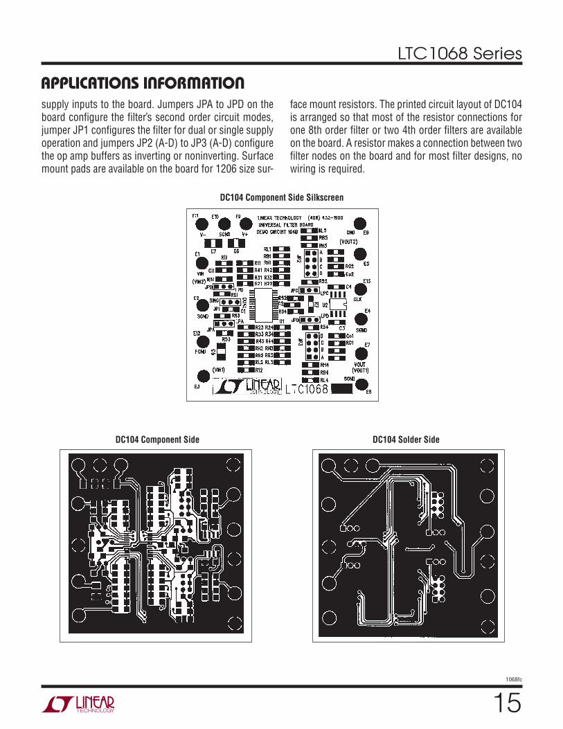
APPLICATIONS INFORMATIONsupply inputs to the board. Jumpers JPA to JPD on the board configure the filter’s second order circuit modes, jumper JP1 configures the filter for dual or single supply operation and jumpers JP2 (A-D) to JP3 (A-D) configure the op amp buffers as inverting or noninverting. Surface mount pads are available on the board for 1206 size sur-
face mount resistors. The printed circuit layout of DC104 is arranged so that most of the resistor connections for one 8th order filter or two 4th order filters are available on the board. A resistor makes a connection between two filter nodes on the board and for most filter designs, no wiring is required.
DC104 Component Side Silkscreen
DC104 Component Side DC104 Solder Side
LTC1068 Series
161068fc
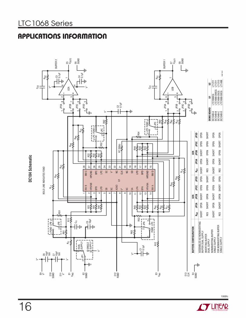
APPLICATIONS INFORMATIONDC
104
Sche
mat
ic
INV
B
HPB/
NB
BPB
LPB
SB NC AGND
V+ NC SA LPA
BPA
HPA/
NA
INV
A
28 27 26 25 24 23 22 21 20 19 18 17 16 15
1 2 3 4 5 6 7 8 9 10 11 12 13 14
INV
C
HPC/
NC BPC
LPC SC V–
NC CLK NC SD LPD
BPD
HPD/
ND
INV
D
U1
R22
R L5
R64
R H4
R B4
R L4
R B5
R H5
R H1
R B1
R L1
R G2
C O2
R32
R42
R21
R11
R I1
C I1
JP1
V–
V+
V+ V–
DUAL
SUPP
LY
E1V I
N2 E3V I
N1
C5 10µF
SING
LESU
PPLY
1 3
2
E13
CLK E4
SGNDE1
0SG
ND E2SG
ND E12
FGND
R61
R31
R41
R24
R43
R33
R23
R H2
R12
R63
R53
R51
R B2
R L2
R H3
BOLD
LIN
E IN
DICA
TES
FGND
R L3
R B3
R34
R44
R7 2
00Ω
R62
R52
13
2JP
C
LPC
FGND
13
2JP
B
LPB
FGND
13
2JP
D
LPD
FGND
R54
– +
27
328
U2A
4
1
V+ V–
V–
C3 0.1µ
F
E5 V OUT
2
BUFF
ER 2
E6 SGND
JP2B
36
JP2C
45
JP2D
18
JP2A
C4 0.1µ
F
C2 0.1µ
F
R G1
C O1
– +
27
56
U2B
7
1068
TA0
3
E7 V OUT
1
BUFF
ER 1
E8 SGND
JP3B
36
JP3C
45
JP3D
18
JP3A
13
2JP
A
LPD
FGND
C1 0.1µ
F
E9 V+
E11 V–
C6 10µF
16V
C7 10µF
16V BU
FFER
S CO
NFIG
URAT
ION
ASSE
MBL
ED A
S NO
NINV
ERTI
NGBU
FFER
DUA
L SU
PPLY
INVE
RTIN
G BU
FFER
DUAL
SUP
PLY
NONI
NVER
TING
BUF
FER
SING
LE S
UPPL
YFO
R NO
NINV
ERTI
NG B
UFFE
RSI
NGLE
SUP
PLY
RG
2
SHOR
T
RES
SHOR
T
RES
JP2A
OPEN
SHOR
T
OPEN
SHOR
T
U2A
JP2B
SHOR
T
OPEN
SHOR
T
OPEN
JP2C
OPEN
OPEN
OPEN
SHOR
T
JP2D
OPEN
SHOR
T
OPEN
OPEN
RG
1
SHOR
T
RES
SHOR
T
RES
JP3A
OPEN
SHOR
T
OPEN
SHOR
T
U2A
JP3B
SHOR
T
OPEN
SHOR
T
OPEN
JP3C
OPEN
OPEN
OPEN
SHOR
T
JP3D
OPEN
SHOR
T
OPEN
OPEN
DEM
O BO
ARD
DC10
4B-A
DC10
4B-B
DC10
4B-C
DC10
4B-D
U
1LT
C106
8CG
LTC1
068-
200C
GLT
C106
8-25
CGLT
C106
8-50
CG
U2
LT12
11LT
1211
LT12
13LT
1498

LTC1068 Series
171068fc
APPLICATIONS INFORMATIONA Surface Mount Printed Circuit Layout
A very compact surface mount printed circuit layout can be designed with 0603 size surface mount resistors, capacitors and a 28-pin SSOP of the LTC1068 product family. An example of a printed circuit layout is shown
in the following figures for an 8th order elliptic bandpass filter. The total board area of this 8th order filter is 1" by 0.8". No attempt was made to design the smallest possible printed circuit layout.
70kHz Elliptic Bandpass Filtter, fCENTER = fCLK/25 (Maximum fCENTER is 80kHz, VS = ±5V)
Gain vs Frequency
INV B INV C281
HPB/NB HPC/NC272
SB
NC
NC
SC245
R21 4.99k R22 4.99k
BPB BPC263R31 24.9k R32 107k
LPA LPD
209
R43 43.2k
R44 17.4kBPA BPD
1910
R33 59k
R34 63.4kHPA/NA HPD/ND
1811
INV A INV D
17
16
15
12
13
14
R23 4.99k
R24 7.5k
LPB LPC254R41 20.5k
R514.99k
RH2 11.3k
R11 29.4kVIN
R64 10k
R62 56.2k
RH1 28k
RH3 15.4kVOUT
AGND
V– 236
V+
227
SA SD
NC
NC
CLK218
5V
–5V
1.75MHz
1068 TA04
U1LTC1068-25
C10.1µF
C20.1µF
R544.99k
R524.99k
RL345.3K
R61 11.3k
RL2 23.2k
FREQUENCY (kHz)20
GAIN
(dB)
10
0
–10
–20
–30
–40
–50
–60
–70
–80
–9040 60 70
1068 TA05
30 50 80 90 100
FilterCAD Custom Inputs for fC = 70kHz2nd ORDER SECTION f0 (kHz) Q fN (kHz) TYPE MODE
B 67.7624 5.7236 58.3011 HPN 2b
C 67.0851 20.5500 81.6810 LPN 1bn
A 73.9324 15.1339 81.0295 LPN 2n
D 73.3547 16.3491 BP 2b

LTC1068 Series
181068fc
APPLICATIONS INFORMATIONSurface Mount Components
(Board Area = 1" × 0.8")
Component Side Solder Side
R11
R22U1
R32R52
R62
R64
R54
RH1
R21
R51
R61
R43
R24
1068 TA06
R34
R44
C2C1
R33
R23
RH2 RL3
RL2 RH3
R31
R41
R61 R41
R43
R33
R23
R31
R21
R11
R22R32 R52
R62
R64
R54
R24
RH3
RH2
RL3
RL2
R34
R44
RH1
R51
GND
1068 TA07
GND
VIN
VOUT
V+
V–
1068 TA08

LTC1068 Series
191068fc
TYPICAL APPLICATIONSLTC1068-200 8th Order Linear Phase Lowpass, fCUTOFF = fCLK/400
for Ultralow Frequency Applications
FilterCAD Custom Inputs for fC = 1Hz2nd ORDER SECTION f0 (kHz) Q QN TYPE MODE
B 1.7947 0.7347 LP 3
C 1.6002 0.5195 LP 1b
A 1.7961 1.1369 1.0159 LPBP 3s
D 1.6070 0.5217 LP 1b
Gain and Group Delayvs Frequency
INV B
HPB/NB
BPB
LPB
SB
NC
AGND
V+
NC
SA
LPA
BPA
HPA/NA
INV A
28
27
26
25
24
23
22
21
20
19
18
17
16
15
1
2
3
4
5
6
7
8
9
10
11
12
13
14
INV C
HPC/NC
BPC
LPC
SC
V–
NC
CLK
NC
SD
LPD
BPD
HPD/ND
INV D
LTC1068-200
RL123.2k
RL214.3k
R21 12.4k R22 15.4k
R32 10k
R52 5.11k
R34 10k
R24 15.4k
R54 5.11k
R64 9.09k
R62 9.09k
R31 10kR11
14.3k
R41 15.4k
R23 10k
R33 12.4k
R43 12.4k
RB3 23.2kRL3 23.2k
0.1µF5V
–5V
400kHz
VOUT
1068 TA09
0.1µF
VIN
FREQUENCY (Hz)0.1
–90
GAIN
(dB)
GROUP DELAY (SEC)
–70
–50
–30
–10
1 10
1068 TA10
10
–80
–60
–40
–20
0
0
0.2
0.4
0.6
0.8
1.0
0.1
0.3
0.5
0.7
0.9GAIN
GROUPDELAY

LTC1068 Series
201068fc
TYPICAL APPLICATIONSLTC1068-50 8th Order Linear Phase Lowpass, fCUTOFF = fCLK/50 for Single Supply Low Power Applications. Maximum fCUTOFF is
20kHz with a 3.3V Supply and 40kHz with a 5V Supply
FilterCAD Custom Inputs for fC = 10kHz2nd ORDER SECTION f0 (kHz) Q fN (kHz) QN TYPE MODE
B 9.5241 0.5248 0.5248 AP 4a3
C 11.0472 1.1258 21.7724 LPN 2n
A 11.0441 1.3392 1.5781 LPBP 2s
D 6.9687 0.6082 LP 3
Gain and Group Delayvs Frequency
INV B
HPB/NB
BPB
LPB
SB
NC
AGND
V+
NC
SA
LPA
BPA
HPA/NA
INV A
28
27
26
25
24
23
22
21
20
19
18
17
16
15
1
2
3
4
5
6
7
8
9
10
11
12
13
14
INV C
HPC/NC
BPC
LPC
SC
V–
NC
CLK
NC
SD
LPD
BPD
HPD/ND
INV D
LTC1068-50
RB113.3k
RH234k
RL29.09k
RA156.2k
R21 20.5k R22 43.2k
R32 43.2k
R42 196k
R34 14.3k
R44 34.8k
R24 16.9k
R31 10kR11
22.6k
R41 22.6k
R23 10.7k
R33 12.7k
R43 48.7k
RB3 24.9kRL3 26.7k
0.1µF
1µF
3.3V 500kHz
VOUT
1068 TA11
VIN
FREQUENCY (kHz)1
GAIN
(dB)
GROUP DELAY (µs)
–70
–50
–30
–10
10 100
1068 TA12
10
–80
–60
–40
–20
0
60
80
100
130
150
70
90
110
120
140GAIN
GROUPDELAY

LTC1068 Series
211068fc
TYPICAL APPLICATIONSLTC1068-25 8th Order Lowpass, fCUTOFF = fCLK/32, Attenuation –50dB at (1.25) (fCUTOFF) and –60dB at
(1.5)(fCUTOFF). Maximum fCUTOFF = 120kHz
FilterCAD Custom Inputs for fC = 100kHz2nd ORDER SECTION f0 (kHz) Q fN (kHz) TYPE MODE
B 70.9153 0.5540 127.2678 LPN 1bn
C 94.2154 2.3848 154.1187 LPN 1bn
A 101.4936 9.3564 230.5192 LPN 1bn
D 79.7030 0.9340 LP 1b
Gain vs FrequencyINV B INV C281
HPB/NB HPC/NC272
SB
NC
NC
SC245
R21 10k R22 10k
BPB BPC263R31 10k R32 32.4k
LPA LPD
209
R63 8.45k
BPA BPD
1910
R33 118k R34 15k
HPA/NA HPD/ND
1811
INV A INV D
17
16
15
12
13
14
R23 10k R24 10k
LPB LPC254
R514.99k
RH2 36.5k
R11 32.4kVIN
R64 3.16k
R62 5.9k
RH1 18.2kRL1
26.7k
RH3 53.6kVOUT
AGND
V– 236
V+
227
SA SD
NC
NC
CLK218
5V
–5V
3.2MHz
1068 TA13
LTC1068-25
0.1µF
0.1µF
R534.99k
R544.99k
R524.99k
RL320.5K
R612.21k
RL2 40.2k
FREQUENCY (kHz)20
–80
GAIN
(dB)
–70
–30
–10
100 500
1069 TA14
10
–40
–50
–60
–20
0
LTC1068 Series
221068fc
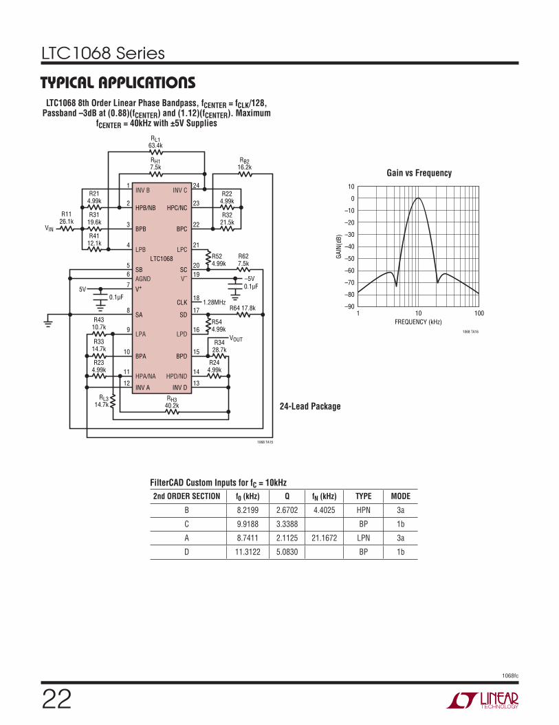
TYPICAL APPLICATIONSLTC1068 8th Order Linear Phase Bandpass, fCENTER = fCLK/128,
Passband –3dB at (0.88)(fCENTER) and (1.12)(fCENTER). Maximum fCENTER = 40kHz with ±5V Supplies
FilterCAD Custom Inputs for fC = 10kHz2nd ORDER SECTION f0 (kHz) Q fN (kHz) TYPE MODE
B 8.2199 2.6702 4.4025 HPN 3a
C 9.9188 3.3388 BP 1b
A 8.7411 2.1125 21.1672 LPN 3a
D 11.3122 5.0830 BP 1b
Gain vs Frequency
INV B INV C241
HPB/NB HPC/NC232
SB SC205
R214.99k
R224.99k
BPB BPC223
R3119.6k
R4112.1k
R3221.5k
LPA LPD169
R4310.7k
BPA BPD1510
R3314.7k
HPA/NA HPD/ND1411
INV A INV D1312
R234.99k
R3428.7k
R244.99k
LPB LPC214
R1126.1k
VIN
RL163.4k
RH17.5k
RB216.2k
RH340.2k
AGND V– 196
V+
CLK18
7
SA SD178
5V
–5V
1.28MHz
1068 TA15
LTC1068 R524.99k
R544.99k
0.1µF
0.1µF
R627.5k
R64 17.8k
RL314.7k
VOUT
FREQUENCY (kHz)1
GAIN
(dB)
10
0
–10
–20
–30
–40
–50
–60
–70
–80
–9010 100
1068 TA16
24-Lead Package

LTC1068 Series
231068fc
TYPICAL APPLICATIONSLTC1068 8th Order Linear Phase Bandpass, fCENTER = fCLK/100,
Passband –3dB at (0.88)(fCENTER) and (1.12)(fCENTER). Maximum fCENTER = 50kHz with ±5V Supplies
FilterCAD Custom Inputs for fC = 10kHz2nd ORDER SECTION f0 (kHz) Q fN (kHz) TYPE MODE
B 10.4569 2.6999 17.4706 LPN 2n
C 11.7607 3.9841 BP 2
A 8.6632 2.1384 BP 2b
D 9.0909 1.8356 BP 3
Gain vs Frequency
24-Lead Package
INV B INV C241
HPB/NB HPC/NC232
SB SC205
R2110k
R2210k
BPB BPC223
R3125.5k
R3232.4k
LPA LPD169
R4316.9k
R632.32k
R4412.1k
BPA BPD1510
R3317.4k
R3419.1k
HPA/NA HPD/ND1411
INV A INV D1312
R237.32k
R2410k
LPB LPC214
R41107k
R4226.1k
R1124.3k
VIN
RL124.9k
RB214.3k
RH151.1k
RB318.7k VOUT
AGND V– 196
V+
fCLK18
7
SA SD 178
5V–5V
1MHz
1068 TA17
LTC10680.1µF
0.1µF
R534.99k
FREQUENCY (kHz)1
GAIN
(dB)
10
0
–10
–20
–30
–40
–50
–60
–70
–80
–9010 100
1068 TA18
LTC1068 Series
241068fc
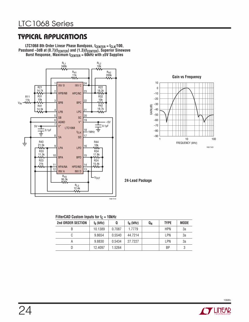
TYPICAL APPLICATIONSLTC1068 8th Order Linear Phase Bandpass, fCENTER = fCLK/100,
Passband –3dB at (0.7)(fCENTER) and (1.3)(fCENTER), Superior Sinewave Burst Response, Maximum fCENTER = 60kHz with ±5V Supplies
FilterCAD Custom Inputs for fC = 10kHz2nd ORDER SECTION f0 (kHz) Q fN (kHz) QN TYPE MODE
B 10.1389 0.7087 1.7779 HPN 3a
C 9.8654 0.5540 44.7214 LPN 3a
A 9.8830 0.5434 27.7227 LPN 3a
D 12.4097 1.5264 BP 3
Gain vs Frequency
24-Lead Package
INV B INV C241
HPB/NB HPC/NC232
SB SC205
R2114.7k
R2218.2k
BPB BPC223
R3110k
R3210k
LPA LPD169
R4321.5k
R4410k
BPA BPD1510
R3311.3k
R3417.8k
HPA/NA HPD/ND1411
INV A INV D1312
R2321k
R2415.4k
LPB LPC214
R4114.3k
R4218.7k
R1111k
VIN
RL1348k
RL210k
RH2200k
RH111k
RH395.3k
RL312.4k
VOUT
AGND V– 196
V+
fCLK18
7
SA SD 178
5V–5V
1MHzLTC1068
0.1µF0.1µF
1068 TA19
FREQUENCY (kHz)1
GAIN
(dB)
10
0
–10
–20
–30
–40
–50
–60
–70
–80
–9010 100
1068 TA20

LTC1068 Series
251068fc
TYPICAL APPLICATIONSLTC1068-50 8th Order Linear Phase Bandpass, fCENTER = fCLK/40,
Passband –3dB at (0.8)(fCENTER) and (1.2)(fCENTER) for Single Supply Low Power Applications. Maximum fCENTER = 25kHz with a Single 5V
Supply
FilterCAD Custom Inputs for fC = 10kHz2nd ORDER SECTION f0 (kHz) Q fN (kHz) TYPE MODE
B 8.7384 4.0091 4.0678 HPN 2b
C 11.6756 4.6752 19.1786 LPN 2n
A 10.8117 4.2066 16.0127 LPN 2n
D 9.6415 3.6831 BP 2
Gain vs FrequencyINV B INV C
281
HPB/NB HPC/NC272
SB
NC
NC
SC245
R21 10k R22 11.3k
BPB BPC263R31 30.1k
R41 10.7k
R32 29.4k
R42 10k
LPA LPD
209
BPA BPD
1910
R33 26.7k
R43 12.1k
R34 28k
R44 22.1k
HPA/NA HPD/ND
1811
INV A INV D
17
16
15
12
13
14
R23 10k R24 10k
LPB LPC254
R514.99k
RH2 84.5k
R11 36.5kVIN
RH1 18.2k
RH3 47.5kVOUT
AGND
V– 236
V+
227
SA SD
NC
NC
CLK218
5V 400kHz
1068 TA21
LTC1068-50
0.1µF1µF
RL315.8K
R611.74k
RL2 17.8k
FREQUENCY (kHz)2 64
–80
GAIN
(dB)
–70
–50
–40
–30
14 18 22
10
1068 TA22
–60
10 128 2826242016
–20
–10
0

LTC1068 Series
261068fc
TYPICAL APPLICATIONSLTC1068-25 8th Order Order Bandpass, fCENTER = fCLK/32, Passband –3dB at (0.965)(fCENTER) and (1.35)(fCENTER).
Maximum fCENTER = 80kHz with ±5V Supplies
FilterCAD Custom Inputs for fC = 10kHz2nd ORDER SECTION f0 (kHz) Q TYPE MODE
B 10.2398 15.6469 BP 1b
C 10.3699 21.1060 BP 1b
A 9.6241 18.6841 LP 1b
D 9.7744 15.6092 LP 1b
Gain vs FrequencyINV B INV C281
HPB/NB HPC/NC272
SB
NC
NC
SC245
R21 4.99k R22 4.99k
BPB BPC263R31 97.6k R32 130k
LPA LPD
209
R63 6.49k
BPA BPD
1910
R33 124k R34 102k
HPA/NA HPD/ND
1811
INV A INV D
17
16
15
12
13
14
R23 4.99k R24 4.99k
LPB LPC254
R514.99k
R11 121kVIN
R64 6.98k
R62 9.53k
RH1 118k
VOUT
AGND
V– 236
V+
227
SA SD
NC
NC
CLK218
5V
–5V
320kHz
1068 TA23
LTC1068-25
0.1µF
0.1µF
R534.99k
R544.99k
R524.99k
RL378.7K
R618.87k
RB2 47.5k
FREQUENCY (kHz)7.5
GAIN
(dB)
10
0
–10
–20
–30
–40
–50
–60
–7011.5
1068 TA24
8.5 9.5 10.5 12.5118 9 10 12

LTC1068 Series
271068fc
Gain vs Frequency
TYPICAL APPLICATIONSLTC1068-200 8th Order Highpass, fCENTER = fCLK/200,
Attenuation –60dB at (0.6)(fCENTER). Maximum fCUTOFF = 20kHz with ±5V Supplies
FilterCAD Custom Inputs for fC = 1kHz2nd ORDER SECTION f0 (kHz) Q fN (kHz) TYPE MODE
B 0.9407 1.5964 0.4212 HPN 3a
C 1.0723 0.5156 0.2869 HPN 3a
A 0.9088 3.4293 0.5815 HPN 2b
D 0.9880 0.7001 0.0000 HP 3
Gain vs FrequencyINV B INV C
281
HPB/NB HPB/NC272
SB
NC
NC
SC245
R21 10k R22 21.5k
BPB BPC263R31 16.5k
R41 11.3k
R32 10.2k
R42 18.7k
LPA LPD
209
BPA BPD
1910
R33 36.5k
R43 20.5kR53
4.99k
R63 2.55k
R34 14.3k
R44 21k
HPA/NA HPD
1811
INV A INV D
17
16
15
12
13
14
R23 10k R24 20.5k
LPB LPC254
RH2 20.5k
R11 18.2kVIN
RH1 11.8kRL1
66.5k
RH3 10k
C23 [1/(2π • R23 • C23) = (160)(fCUTOFF)]VOUT
AGND
V– 236
V+
227
SA SD
NC
NC
CLK218
5V 200kHz
–5V
1068 TA25
LTC1068-200
0.1µF
0.1µF
RL2 249k
FREQUENCY (kHz)0.2
–40
–50
–60
–70
–80
GAIN
(dB) –30
–20
–10
0
1 10
1068 TA26
10

LTC1068 Series
281068fc
PACKAGE DESCRIPTIONPlease refer to http://www.linear.com/designtools/packaging/ for the most recent package drawings.
G28 SSOP 0204
0.09 – 0.25(.0035 – .010)
0° – 8°
0.55 – 0.95(.022 – .037)
5.00 – 5.60**(.197 – .221)
7.40 – 8.20(.291 – .323)
1 2 3 4 5 6 7 8 9 10 11 12 1413
9.90 – 10.50*(.390 – .413)
2526 22 21 20 19 18 17 16 1523242728
2.0(.079)MAX
0.05(.002)MIN
0.65(.0256)
BSC0.22 – 0.38
(.009 – .015)TYPMILLIMETERS
(INCHES)
DIMENSIONS DO NOT INCLUDE MOLD FLASH. MOLD FLASH SHALL NOT EXCEED .152mm (.006") PER SIDEDIMENSIONS DO NOT INCLUDE INTERLEAD FLASH. INTERLEAD FLASH SHALL NOT EXCEED .254mm (.010") PER SIDE
*
**
NOTE:1. CONTROLLING DIMENSION: MILLIMETERS
2. DIMENSIONS ARE IN
3. DRAWING NOT TO SCALE
0.42 ±0.03 0.65 BSC
5.3 – 5.77.8 – 8.2
RECOMMENDED SOLDER PAD LAYOUT
1.25 ±0.12
G Package28-Lead Plastic SSOP (5.3mm)(Reference LTC DWG # 05-08-1640)
N24 REV I 0711
.255 ±.015*(6.477 ±0.381)
1.280*(32.512)
MAX
1 2 3 4 5 6 7 8 9 10
19
11 12
131416 1517182021222324
.020(0.508)
MIN
.120(3.048)
MIN
.130 ±.005(3.302 ±0.127)
.065(1.651)
TYP
.045 – .065(1.143 – 1.651)
.018 ±.003(0.457 ±0.076)
.008 – .015(0.203 – 0.381)
.300 – .325(7.620 – 8.255)
.325+.035–.015+0.889–0.3818.255( )
NOTE:1. DIMENSIONS ARE
INCHESMILLIMETERS
*THESE DIMENSIONS DO NOT INCLUDE MOLD FLASH OR PROTRUSIONS. MOLD FLASH OR PROTRUSIONS SHALL NOT EXCEED .010 INCH (0.254mm)
.100(2.54)BSC
N Package24-Lead PDIP (Narrow .300 Inch)
(Reference LTC DWG # 05-08-1510 Rev I)

LTC1068 Series
291068fc
Information furnished by Linear Technology Corporation is believed to be accurate and reliable. However, no responsibility is assumed for its use. Linear Technology Corporation makes no representa-tion that the interconnection of its circuits as described herein will not infringe on existing patent rights.
REVISION HISTORYREV DATE DESCRIPTION PAGE NUMBER
C 10/12 Correction to Electrical Characteristics table to identify characteristics of LTC1068-50 5
(Revision history begins at Rev C)
LTC1068 Series
301068fc
Linear Technology Corporation1630 McCarthy Blvd., Milpitas, CA 95035-7417 (408) 432-1900 FAX: (408) 434-0507 www.linear.com LINEAR TECHNOLOGY CORPORATION 1996
LT 1012 REV C • PRINTED IN USA
RELATED PARTS
TYPICAL APPLICATION
PART NUMBER DESCRIPTION COMMENTS
LTC1064 Universal Filter, Quad 2nd Order 50:1 and 100:1 Clock-to-fO Ratios, fO to 100kHz, VS = Up to ±7.5V
LTC1067/LTC1067-50 Low Power, Dual 2nd Order Rail-to-Rail, VS = 3V to ±5V
LTC1164 Low Power Universal Filter, Quad 2nd Order 50:1 and 100:1 Clock-to-fO Ratios, fO to 20kHz, VS = Up to ±7.5V
LTC1264 High Speed Universal Filter, Quad 2nd Order 20:1 Clock-to-fO Ratio, fO to 200kHz, VS = Up to ±7.5V
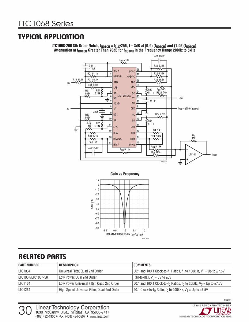
LTC1068-200 8th Order Notch, fNOTCH = fCLK/256, f – 3dB at (0.9) (fNOTCH) and (1.05)(fNOTCH), Attenuation at fNOTCH Greater Than 70dB for fNOTCH in the Frequency Range 200Hz to 5kHz
Gain vs Frequency
INV B INV C281
HPB/NB HPB/NC272
SB
NC
NC
SC245
R21 5.11k R22 6.34k
BPB BPC263R31 51.1k
R41 100k
R32 84.3k
LPA LPD
209R63
8.06k
BPA BPD
1910
R43178k
C23 470pF
R34 75k
HPA/NA HPD
1811
INV A INV D
17
16
15
12
13
14
R33 124k
R23 10k
R24 7.32k
RH4 5.11k
RL4 475k
LPB LPC254
R515.11k
RH2 5.11k
R11 51.1kVIN
R64 7.87k
RG15k
R62 5.76kRL2 66.5k
RH1 5.11k
RH3 5.11k
AGND
V– 236
V+
227
SA SD
NC
NC
CLK218
5V
–5V
fCLK = (256)(fNOTCH)
VOUT
1068 TA27
LTC1068-200
0.1µF
C21470pF
0.1µF
R535.11k
R545.11k
R525.11k
R618.06k
C22 470pF
–
+LT1354
RELATIVE FREQUENCY (fIN/fNOTCH)
GAIN
(dB) –30
–10
10
1.1
1068 TA28
–50
–70
–40
–20
0
–60
–80
–900.8 0.9 1.0 1.2