ltc1702a - dual 550khz synchronous 2-phase … · 1 ltc1702a 1702afa dual 550khz synchronous...
TRANSCRIPT
1
LTC1702A
1702afa
Dual 550kHz Synchronous2-Phase Switching Regulator Controller
The LTC®1702A is a dual switching regulator controlleroptimized for high efficiency with low input voltages. Itincludes two complete, on-chip, independent switching regu-lator controllers each designed to drive a pair of external N-channel MOSFETs in a voltage mode feedback, synchronousbuck configuration. The LTC1702A uses a constant-fre-quency, true PWM design switching at 550kHz, minimizingexternal component size and cost and maximizing loadtransient performance. The synchronous buck architectureautomatically shifts to discontinuous and then to BurstMode® operation as the output load decreases, ensuringmaximum efficiency over a wide range of load currents.The LTC1702A features an onboard reference trimmed to0.5% and can provide better than 1% regulation at theconverter outputs. Open-drain logic outputs indicate whethereither output has risen to within 5% of the final output voltageand an optional latching FAULT mode protects the load if theoutput rises 15% above the intended voltage. Each channelcan be enabled independently; with both channels disabled,the LTC1702A shuts down and supply current drops below100µA.
Pin Compatible with the LTC1702 with ImprovedCurrent Limit Control
Two Sides Run Out-of-Phase to Minimize CIN No External Current Sense Resistors Excellent Output Regulation: 1% Total Output
Accuracy Two Independent Controllers in One Package All N-Channel External MOSFET Architecture 550kHz Switching Frequency Minimizes External
Component Size 1A to 25A Output Current per Channel High Efficiency over Wide Load Current Range Less Than 100µA Shutdown Current Small 24-Pin Narrow SSOP Package
, LT, LTC and LTM are registered trademarks of Linear Technology Corporation.Burst Mode is a registered trademark of Linear Technology Corporation. All other trademarksare the property of their respective owners. Protected by U.S. Patents including 6144194.
Microprocessor, DSP Core and I/O Supplies Multiple Logic Supply Generator Distributed Power Applications High Efficiency Power Conversion
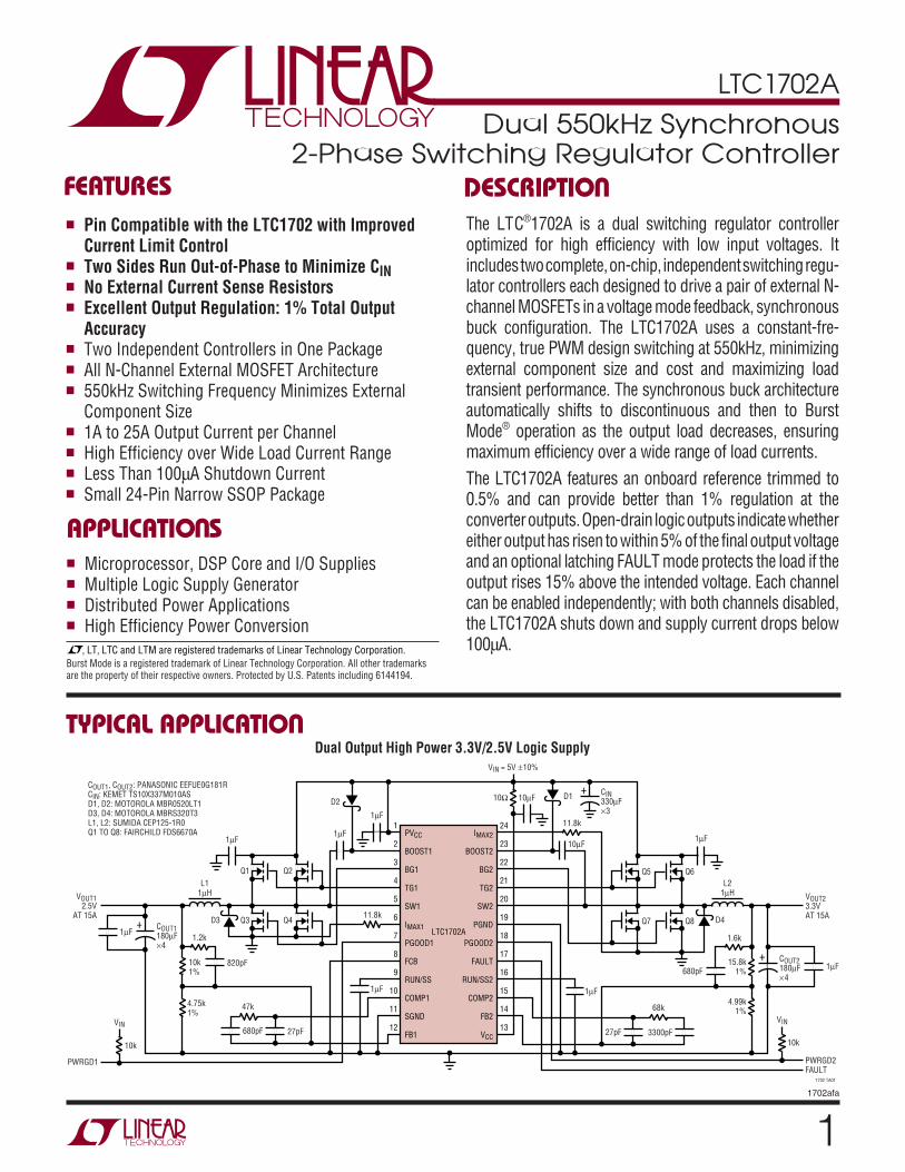
Dual Output High Power 3.3V/2.5V Logic Supply
DESCRIPTIO
U
FEATURES
APPLICATIO SU
TYPICAL APPLICATIO
U
LTC1702A
PVCC
BOOST1
BG1
TG1
SW1
IMAX1
PGOOD1
FCB
RUN/SS
COMP1
SGND
FB1
IMAX2
BOOST2
BG2
TG2
SW2
PGND
PGOOD2
FAULT
RUN/SS2
COMP2
FB2
VCC
1
2
3
4
5
6
7
8
9
10
11
12
24
23
22
21
20
19
18
17
16
15
14
13
1µF
10Ω
1µF1µF
11.8k
11.8k
1.6k
68k
1702 TA01
VIN
1.2k
10k1%
COUT1180µF×4
820pF
27pF680pF
47k
1µF
VOUT12.5V
AT 15A
1µF
4.75k1%
Q2Q1
Q4Q3D3
D2
COUT1, COUT2: PANASONIC EEFUE0G181RCIN: KEMET TS10X337M010ASD1, D2: MOTOROLA MBR0520LT1D3, D4: MOTOROLA MBRS320T3L1, L2: SUMIDA CEP125-1R0Q1 TO Q8: FAIRCHILD FDS6670A
D1
PWRGD1
L11µH
+
10µF
10µF1µF
VIN = 5V ±10%
1µF
CIN330µF×3
+
Q7
Q5
Q8
Q6
D4
680pF
27pF 3300pF
15.8k1%
4.99k1%
10k
L21µH
COUT2180µF×4
1µF
VOUT23.3VAT 15A
PWRGD2FAULT
+
VIN
10k
2
LTC1702A
1702afa
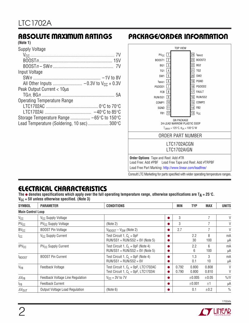
ABSOLUTE MAXIMUM RATINGS
W WW U
(Note 1)
Supply VoltageVCC ........................................................................................... 7VBOOSTn............................................................... 15VBOOSTn – SWn .................................................... 7V
Input VoltageSWn .......................................................... –1V to 8VAll Other Inputs ......................... –0.3V to VCC + 0.3V
Peak Output Current < 10µsTGn, BGn ............................................................... 5A
Operating Temperature RangeLTC1702AC ............................................. 0°C to 70°CLTC1702AI ........................................ –40°C to 85°C
Storage Temperature Range ................. –65°C to 150°CLead Temperature (Soldering, 10 sec).................. 300°C
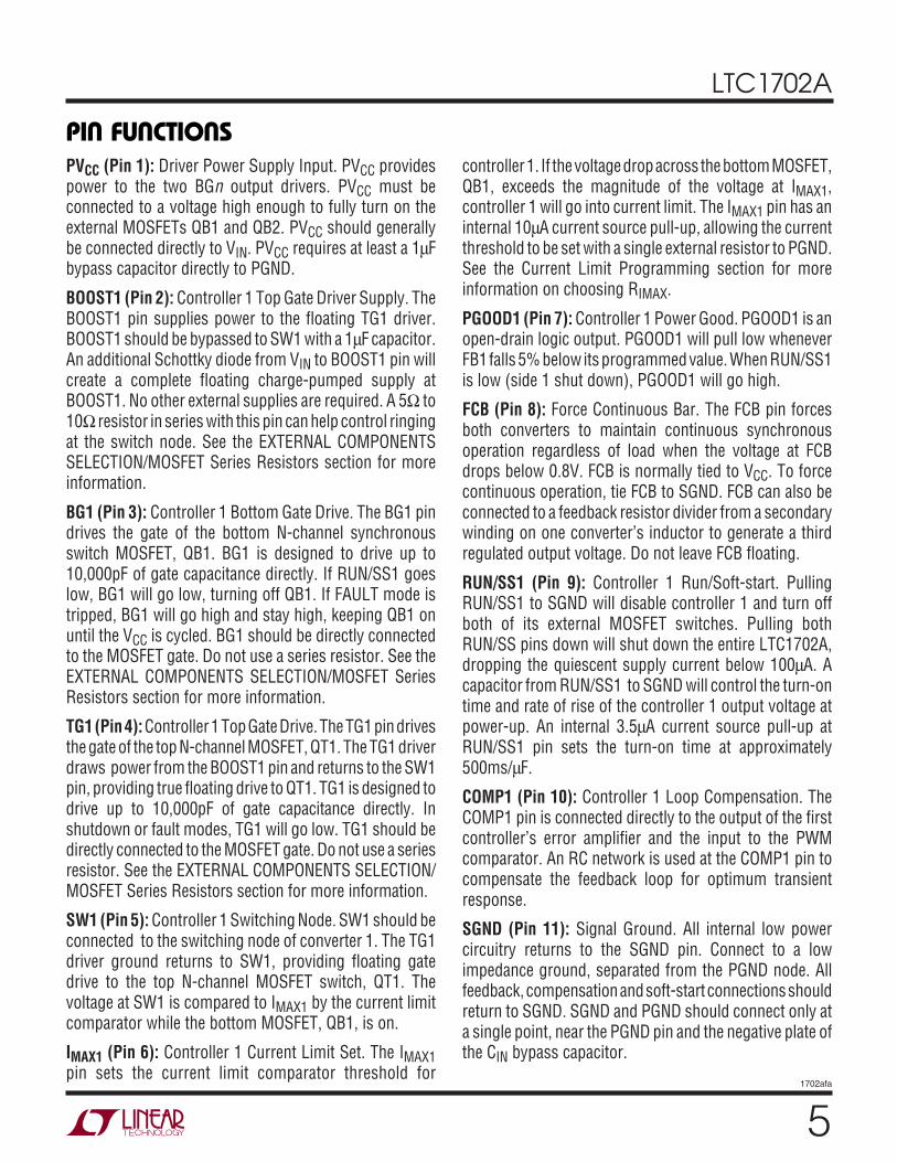
PACKAGE/ORDER INFORMATION
W UU
ELECTRICAL CHARACTERISTICSThe denotes specifications which apply over the full operating temperature range, otherwise specifications are TA = 25°C.VCC = 5V unless otherwise specified. (Note 3)
1
2
3
4
5
6
7
8
9
10
11
12
TOP VIEW
GN PACKAGE24-LEAD NARROW PLASTIC SSOP
24
23
22
21
20
19
18
17
16
15
14
13
PVCC
BOOST1
BG1
TG1
SW1
IMAX1
PGOOD1
FCB
RUN/SS1
COMP1
SGND
FB1
IMAX2
BOOST2
BG2
TG2
SW2
PGND
PGOOD2
FAULT
RUN/SS2
COMP2
FB2
VCC
TJMAX = 125°C, θJA = 100°C/ W
LTC1702ACGNLTC1702AIGN
ORDER PART NUMBER
Consult LTC Marketing for parts specified with wider operating temperature ranges.
Order Options Tape and Reel: Add #TRLead Free: Add #PBF Lead Free Tape and Reel: Add #TRPBFLead Free Part Marking: http://www.linear.com/leadfree/
SYMBOL PARAMETER CONDITIONS MIN TYP MAX UNITS
Main Control Loop
VCC VCC Supply Voltage 3 7 V
PVCC PVCC Supply Voltage (Note 2) 3 7 V
BVCC BOOST Pin Voltage VBOOST – VSW (Note 2) 2.7 7 V
ICC VCC Supply Current Test Circuit 1, CL = 0pF 2.2 8 mARUN/SS1 = RUN/SS2 = 0V (Note 5) 30 100 µA
IPVCC PVCC Supply Current Test Circuit 1, CL = 0pF (Note 4) 2.2 6 mARUN/SS1 = RUN/SS2 = 0V (Note 5) 6 100 µA
IBOOST BOOST Pin Current Test Circuit 1, CL = 0pF (Note 4) 1.3 3 mARUN/SS1 = RUN/SS2 = 0V 0.1 10 µA
VFB Feedback Voltage Test Circuit 1, CL = 0pF, LTC1702AC 0.792 0.800 0.808 VTest Circuit 1, CL = 0pF, LTC1702AI 0.790 0.800 0.810 V
∆VFB Feedback Voltage Line Regulation VCC = 3V to 7V ±0.005 ±0.05 %/V
IFB Feedback Current ±0.001 ±1 µA
∆VOUT Output Voltage Load Regulation (Note 6) 0.1 ±0.2 %

3
LTC1702A
1702afa
ELECTRICAL CHARACTERISTICS
Note 1: Stresses beyond those listed under Absolute Maximum Ratingsmay cause permanent damage to the device. Exposure to any AbsoluteMaximum Rating condition for extended periods may affect devicereliability and lifetime.Note 2: PVCC and BVCC (VBOOST – VSW) must be greater than VGS(ON) ofthe external MOSFETs used to ensure proper operation.Note 3: All currents into device pins are positive; all currents out of devicepins are negative. All voltages are referenced to ground unless otherwisespecified.
Note 4: Supply current in normal operation is dominated by the currentneeded to charge and discharge the external MOSFET gates. This currentwill vary with supply voltage and the external MOSFETs used.Note 5: Supply current in shutdown is dominated by external MOSFETleakage and may be significantly higher than the quiescent current drawnby the LTC1702A, especially at elevated temperature.Note 6: This parameter is guaranteed by correlation and is not testeddirectly.Note 7: Rise and fall times are measured using 10% and 90% levels. Delayand nonoverlap times are measured using 50% levels.
The denotes specifications which apply over the full operating temperature range, otherwise specifications are TA = 25°C.VCC = 5V unless otherwise specified. (Note 3)
SYMBOL PARAMETER CONDITIONS MIN TYP MAX UNITS
VFCB FCB Threshold 0.75 0.8 0.85 V
∆VFCB FCB Feedback Hysteresis 20 mV
IFCB FCB Pin Current ±0.001 ±1 µA
VRUN RUN/SS Pin RUN Threshold 0.45 0.55 0.65 V
ISS Soft-Start Source Current RUN/SSn = 0V –2 –3.5 –6 µA
Maximum Soft-Start Sink Current VIMAX = 0V, VSW = –0.5V 1 mA
IMAX IMAX Source Current VIMAX = 0V –12 –10 –8 µA
Switching Characteristics
fOSC Oscillator Frequency Test Circuit 1, CL = 0pF 475 550 750 kHz
ΦOSC2 Converter 2 Oscillator Phase Relative to Converter 1 (Note 6) 180 DEG
DCMIN Minimum Duty Cycle 0 %
DCMAX Maximum Duty Cycle 87 90 93 %
tNOV Driver Nonoverlap Test Circuit 1, CL = 2000pF (Note 7) 40 100 ns
tr, tf Driver Rise/Fall Time Test Circuit 1, CL = 2000pF (Note 7) 12 80 ns
Feedback Amplifier
AVFB FB DC Gain 74 85 dB
GBW FB Gain Bandwidth 25 MHz
IERR FB Sink/Source Current ±3 ±10 mA
Status Outputs
VPGOOD PGOOD Trip Point VFB Relative to Regulated VOUT –10 –5 –2 %
VOLPG PGOOD Output Low Voltage PGOOD = 1mA 0.03 0.1 V
IPGOOD PGOOD Output Leakage ±0.1 ±1 µA
tPGOOD PGOOD Delay Time VFB < VPGOOD to PGOOD (Note 7) 100 µs
VFAULT FAULT Trip Point VFB Relative to Regulated VOUT 10 15 20 %
VOLF FAULT Output Low Voltage IFAULT = 1mA 0.03 0.1 V
IFAULT FAULT Output Current VFAULT = 0V –10 µA
tFAULT FAULT Delay Time VFB > VFAULT to FAULT (Note 7) 25 µs

4
LTC1702A
1702afa
TYPICAL PERFOR A CE CHARACTERISTICS
UW
Efficiency vs Load Current
TEMPERATURE (°C)–50
SUPP
LY C
URRE
NT (m
A)
2.4 PVCC
VCC
25
1702A G04
1.8
1.4
–25 0 50
1.2
1.0
2.6
2.2
2.0
1.6
75 100 125
BOOST1, BOOST2
TEST CIRCUIT 1CL = 0pF
Transient Response
TEMPERATURE (°C)–50
–2.5
NORM
ALIZ
ED O
SCIL
LATO
R FR
EQUE
NCY
(%)
–2.0
–1.0
–0.5
0
2.5
1.0
0 50 75
1702A G05
–1.5
1.5
2.0
0.5
–25 25 100 125
VCC = 5V
TEMPERATURE (°C)–50
0.4
R ON
(Ω)
0.5
0.7
0.8
0.9
1.4
1.1
0 50 75
1702A G06
0.6
1.2
1.3
1.0
–25 25 100 125
VPVCC = 5VVBOOST – VSW = 5V
MOSFET Driver Supply Currentvs Gate Capacitance
Supply Current vs TemperatureNormalized Oscillator Frequencyvs Temperature Driver RON vs Temperature
RUN/SS Source Currentvs Temperature
TEMPERATURE (°C)–50
SOUR
CE C
URRE
NT (µ
A)
4.0
4.5
5.0
25 75
1702A G07
3.5
3.0
–25 0 50 100 125
2.5
2.0
VCC = 5V
Nonoverlap Time vs Temperature Driver Rise/Fall vs Temperature
LOAD CURRENT (A)0
70
EFFI
CIEN
CY (%
)
80
90
100
5 10
1702A G01
15
VIN = 5VVOUT = 3.3V
VOUT = 2.5V
VOUT = 1.6V
VIN = 5VVOUT = 1.8VILOAD = 0A-10A-0A±2.2% MAX DEVIATION
1702A G02
GATE CAPACITANCE (pF)0
25
30
35
6000 8000
1702A G03
20
15
2000 4000 10000
10
5
0
DRIV
ER S
UPPL
Y CU
RREN
T (m
A)
TEST CIRCUIT 1ONE DRIVER LOADEDMULTIPLY BY # OF ACTIVEDRIVERS TO OBTAIN TOTALDRIVER SUPPLY CURRENT
TEMPERATURE (°C)–50
40
50
70
25 75
1702A G08
30
20
–25 0 50 100 125
10
0
60
NONO
VERL
AP (n
s)
TEST CIRCUIT 1CL = 2000pF
BG FALLING EDGETG RISING EDGE
TG FALLING EDGEBG RISING EDGE
TEMPERATURE (°C)–50 –25
12
RISE
/FAL
L TI
ME
(ns)
12
15
0 50 75
1702A G09
11
14
13
25 100 125
TEST CIRCUIT 1CL = 2000pF
IL20mV/DIV
10µs/DIV
5
LTC1702A
1702afa
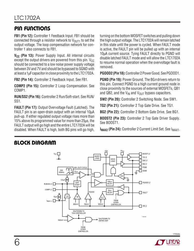
PIN FUNCTIONS
UUU
controller 1. If the voltage drop across the bottom MOSFET,QB1, exceeds the magnitude of the voltage at IMAX1,controller 1 will go into current limit. The IMAX1 pin has aninternal 10µA current source pull-up, allowing the currentthreshold to be set with a single external resistor to PGND.See the Current Limit Programming section for moreinformation on choosing RIMAX.
PGOOD1 (Pin 7): Controller 1 Power Good. PGOOD1 is anopen-drain logic output. PGOOD1 will pull low wheneverFB1 falls 5% below its programmed value. When RUN/SS1is low (side 1 shut down), PGOOD1 will go high.
FCB (Pin 8): Force Continuous Bar. The FCB pin forcesboth converters to maintain continuous synchronousoperation regardless of load when the voltage at FCBdrops below 0.8V. FCB is normally tied to VCC. To forcecontinuous operation, tie FCB to SGND. FCB can also beconnected to a feedback resistor divider from a secondarywinding on one converter’s inductor to generate a thirdregulated output voltage. Do not leave FCB floating.
RUN/SS1 (Pin 9): Controller 1 Run/Soft-start. PullingRUN/SS1 to SGND will disable controller 1 and turn offboth of its external MOSFET switches. Pulling bothRUN/SS pins down will shut down the entire LTC1702A,dropping the quiescent supply current below 100µA. Acapacitor from RUN/SS1 to SGND will control the turn-ontime and rate of rise of the controller 1 output voltage atpower-up. An internal 3.5µA current source pull-up atRUN/SS1 pin sets the turn-on time at approximately500ms/µF.
COMP1 (Pin 10): Controller 1 Loop Compensation. TheCOMP1 pin is connected directly to the output of the firstcontroller’s error amplifier and the input to the PWMcomparator. An RC network is used at the COMP1 pin tocompensate the feedback loop for optimum transientresponse.
SGND (Pin 11): Signal Ground. All internal low powercircuitry returns to the SGND pin. Connect to a lowimpedance ground, separated from the PGND node. Allfeedback, compensation and soft-start connections shouldreturn to SGND. SGND and PGND should connect only ata single point, near the PGND pin and the negative plate ofthe CIN bypass capacitor.
PVCC (Pin 1): Driver Power Supply Input. PVCC providespower to the two BGn output drivers. PVCC must beconnected to a voltage high enough to fully turn on theexternal MOSFETs QB1 and QB2. PVCC should generallybe connected directly to VIN. PVCC requires at least a 1µFbypass capacitor directly to PGND.
BOOST1 (Pin 2): Controller 1 Top Gate Driver Supply. TheBOOST1 pin supplies power to the floating TG1 driver.BOOST1 should be bypassed to SW1 with a 1µF capacitor.An additional Schottky diode from VIN to BOOST1 pin willcreate a complete floating charge-pumped supply atBOOST1. No other external supplies are required. A 5Ω to10Ω resistor in series with this pin can help control ringingat the switch node. See the EXTERNAL COMPONENTSSELECTION/MOSFET Series Resistors section for moreinformation.
BG1 (Pin 3): Controller 1 Bottom Gate Drive. The BG1 pindrives the gate of the bottom N-channel synchronousswitch MOSFET, QB1. BG1 is designed to drive up to10,000pF of gate capacitance directly. If RUN/SS1 goeslow, BG1 will go low, turning off QB1. If FAULT mode istripped, BG1 will go high and stay high, keeping QB1 onuntil the VCC is cycled. BG1 should be directly connectedto the MOSFET gate. Do not use a series resistor. See theEXTERNAL COMPONENTS SELECTION/MOSFET SeriesResistors section for more information.
TG1 (Pin 4): Controller 1 Top Gate Drive. The TG1 pin drivesthe gate of the top N-channel MOSFET, QT1. The TG1 driverdraws power from the BOOST1 pin and returns to the SW1pin, providing true floating drive to QT1. TG1 is designed todrive up to 10,000pF of gate capacitance directly. Inshutdown or fault modes, TG1 will go low. TG1 should bedirectly connected to the MOSFET gate. Do not use a seriesresistor. See the EXTERNAL COMPONENTS SELECTION/MOSFET Series Resistors section for more information.
SW1 (Pin 5): Controller 1 Switching Node. SW1 should beconnected to the switching node of converter 1. The TG1driver ground returns to SW1, providing floating gatedrive to the top N-channel MOSFET switch, QT1. Thevoltage at SW1 is compared to IMAX1 by the current limitcomparator while the bottom MOSFET, QB1, is on.
IMAX1 (Pin 6): Controller 1 Current Limit Set. The IMAX1pin sets the current limit comparator threshold for
6
LTC1702A
1702afa
FB1 (Pin 12): Controller 1 Feedback Input. FB1 should beconnected through a resistor network to VOUT1 to set theoutput voltage. The loop compensation network for con-troller 1 also connects to FB1.
VCC (Pin 13): Power Supply Input. All internal circuitsexcept the output drivers are powered from this pin. VCCshould be connected to a low noise power supply voltagebetween 3V and 7V and should be bypassed to SGND withat least a 1µF capacitor in close proximity to the LTC1702A.
FB2 (Pin 14): Controller 2 Feedback Input. See FB1.
COMP2 (Pin 15): Controller 2 Loop Compensation. SeeCOMP1.
RUN/SS2 (Pin 16): Controller 2 Run/Soft-start. See RUN/SS1.
FAULT (Pin 17): Output Overvoltage Fault (Latched). TheFAULT pin is an open-drain output with an internal 10µApull-up. If either regulated output voltage rises more than15% above its programmed value for more than 25µs, theFAULT output will go high and the entire LTC1702A will bedisabled. When FAULT is high, both BG pins will go high,
PIN FUNCTIONS
UUU
turning on the bottom MOSFET switches and pulling downthe high output voltage. The LTC1702A will remain latchedin this state until the power is cycled. When FAULT modeis active, the FAULT pin will be pulled up with an internal10µA current source. Tying FAULT directly to PGND willdisable latched FAULT mode and will allow the LTC1702Ato resume normal operation when the overvoltage fault isremoved.
PGOOD2 (Pin 18): Controller 2 Power Good. See PGOOD1.
PGND (Pin 19): Power Ground. The BGn drivers return tothis pin. Connect PGND to a high current ground node inclose proximity to the sources of external MOSFETs, QB1and QB2, and the VIN and VOUT bypass capacitors.
SW2 (Pin 20): Controller 2 Switching Node. See SW1.
TG2 (Pin 21): Controller 2 Top Gate Drive. See TG1.
BG2 (Pin 22): Controller 2 Bottom Gate Drive. See BG1.
BOOST2 (Pin 23): Controller 2 Top Gate Driver Supply.See BOOST1.
IMAX2 (Pin 24): Controller 2 Current Limit Set. See IMAX1.
BLOCK DIAGRAM
W
BURSTLOGIC
SOFTSTART
90% DUTY CYCLE
RUN/SS1,2
COMP1,2
10µA
3.5µA
1VP-P
550mV
800mV 760mV
IMAX1,2
DRIVELOGIC
100µsDELAY
OSC550kHz
+ –ILIM FB
PGOOD
920mV
FLT
DIS
FCB
FB1,2
1702A BD
BOOST1,2
TG1,2
FROMOTHER
CONTROLLER
SHUTDOWN TOTHIS CONTROLLER
SHUTDOWN TOENTIRE CHIP
FAULT
PVCC
25µsDELAY
FROMOTHER
CONTROLLER
VCC
SW1,2
BG1,2
PGND
SGND
PGOOD1,2
7
LTC1702A
1702afa
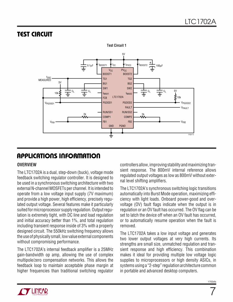
TEST CIRCUIT Test Circuit 1
controllers allow, improving stability and maximizing tran-sient response. The 800mV internal reference allowsregulated output voltages as low as 800mV without exter-nal level shifting amplifiers.
The LTC1702A’s synchronous switching logic transitionsautomatically into Burst Mode operation, maximizing effi-ciency with light loads. Onboard power-good and over-voltage (OV) fault flags indicate when the output is inregulation or an OV fault has occurred. The OV flag can beset to latch the device off when an OV fault has occurred,or to automatically resume operation when the fault isremoved.
The LTC1702A takes a low input voltage and generatestwo lower output voltages at very high currents. Itsstrengths are small size, unmatched regulation and tran-sient response and high efficiency. This combinationmakes it ideal for providing multiple low voltage logicsupplies to microprocessors or high density ASICs, insystems using a “2-step” regulation architecture commonin portable and advanced desktop computers.
OVERVIEW
The LTC1702A is a dual, step-down (buck), voltage modefeedback switching regulator controller. It is designed tobe used in a synchronous switching architecture with twoexternal N-channel MOSFETs per channel. It is intended tooperate from a low voltage input supply (7V maximum)and provide a high power, high efficiency, precisely regu-lated output voltage. Several features make it particularlysuited for microprocessor supply regulation. Output regu-lation is extremely tight, with DC line and load regulationand initial accuracy better than 1%, and total regulationincluding transient response inside of 3% with a properlydesigned circuit. The 550kHz switching frequency allowsthe use of physically small, low value external componentswithout compromising performance.
The LTC1702A’s internal feedback amplifier is a 25MHzgain-bandwidth op amp, allowing the use of complexmultipole/zero compensation networks. This allows thefeedback loop to maintain acceptable phase margin athigher frequencies than traditional switching regulator
APPLICATIONS INFORMATIONWU UU
VCC
5V
5V
10k
2k
CL CL CL CL
BOOST1
TG1
BG1
SW1
IMAX1
FCB
PGOOD1
RUN/SS1
COMP1
FB1
LTC1702A
BOOST2
TG2
BG2
SW2
IMAX2
PGOOD2
FAULT
RUN/SS2
COMP2
FB2
0.1µF 100µF
VPGOOD1
VFB1 VFB2
VPGOOD2
VFAULT
IBOOST1 ICC IPVCC IBOOST2
fOSCMEASURED
1702A TC
PVCC
GND PGND
+
2k
5V
10k

8
LTC1702A
1702afa
2-Step Conversion
“2-step” architectures use a primary regulator to convertthe input power source (batteries or AC line voltage) to anintermediate supply voltage, often 5V. This intermediatevoltage is then converted to the low voltage, high currentsupplies required by the system using a secondary regu-lator—the LTC1702A. 2-step conversion eliminates theneed for a single converter that converts a high inputvoltage to a very low output voltage, often an awkwarddesign challenge. It also fits naturally into systems thatcontinue to use the 5V supply to power portions of theircircuitry, or have excess 5V capacity available as newercircuit designs shift the current load to lower voltagesupplies.
Each regulator in a typical 2-step system maintains arelatively low step-down ratio (5:1 or less), running at highefficiency while maintaining a reasonable duty cycle. Incontrast, a regulator taking a single step from a high inputvoltage to a 1.xV or 2.xV output must run at a very narrowduty cycle, mandating trade-offs in external componentvalues and compromising efficiency and transientresponse. The efficiency loss can exceed that of using a2-step solution (see the 2-Step Efficiency Calculationsection and Figure 14). Further complicating the calcula-tion is the fact that many systems draw a significantfraction of their total power off the intermediate 5V supply,bypassing the low voltage supply. 2-step solutions usingthe LTC1702A usually match or exceed the total systemefficiency of single-step solutions, and provide the addi-tional benefits of improved transient response, reducedPCB area and simplified power trace routing.
2-step regulation can buy advantages in thermal manage-ment as well. Power dissipation in the LTC1702A portionof a 2-step circuit is lower than it would be in a typical 1-step converter, even in cases where the 1-step converterhas higher total efficiency than the 2-step system. In atypical microprocessor core supply regulator, for ex-ample, the regulator is usually located right next to theCPU. In a 1-step design, all of the power dissipated by thecore regulator is right there next to the hot CPU, aggravat-ing thermal management. In a 2-step LTC1702A design,a significant percentage of the power lost in the core
APPLICATIONS INFORMATION
WU UU
regulation system happens in the 5V supply, which isusually located away from the CPU. The power lost to heatin the LTC1702A section of the system is relatively low,minimizing the added heat near the CPU.
See the Optimizing Performance section for a detailedexplanation of how to calculate system efficiency.
2-Phase Operation
The LTC1702A dual switching regulator controller alsofeatures the considerable benefits of 2-phase operation.Notebook computers, hand-held terminals and automo-tive electronics all benefit from the lower input filteringrequirement, reduced electromagnetic interference (EMI)and increased efficiency associated with 2-phaseoperation.
Why the need for 2-phase operation? Up until theLTC1702A, constant-frequency dual switching regulatorsoperated both channels in phase (i.e., single-phase opera-tion). This means that both topside MOSFETs turned on atthe same time, causing current pulses of up to twice theamplitude of those for one regulator to be drawn from theinput capacitor. These large amplitude current pulsesincreased the total RMS current flowing from the inputcapacitor, requiring the use of more expensive inputcapacitors and increasing both EMI and losses in the inputcapacitor and input power supply.
With 2-phase operation, the two channels of the LTC1702Aare operated 180 degrees out of phase. This effectivelyinterleaves the current pulses coming from the switches,greatly reducing the overlap time where they add together.The result is a significant reduction in total RMS inputcurrent, which in turn allows less expensive input capaci-tors to be used, reduces shielding requirements for EMIand improves real world operating efficiency.
Figure 7 shows example waveforms for a single switchingregulator channel versus a 2-phase LTC1702A systemwith both sides switching. A single-phase dual regulatorwith both sides operating would exhibit double the singleside numbers. In this example, 2-phase operation reducedthe RMS input current from 9.3ARMS (2 × 4.66ARMS) to4.8ARMS. While this is an impressive reduction in itself,

9
LTC1702A
1702afa
APPLICATIONS INFORMATION
WU UU
remember that the power losses are proportional to IRMS2,
meaning that the actual power wasted is reduced by afactor of 3.75. The reduced input ripple voltage also meansless power is lost in the input power path, which couldinclude batteries, switches, trace/connector resistancesand protection circuitry. Improvements in both conductedand radiated EMI also directly accrue as a result of thereduced RMS input current and voltage.
Small Footprint
The LTC1702A operates at a 550kHz switching frequency,allowing it to use low value inductors without generatingexcessive ripple currents. Because the inductor storesless energy per cycle, the physical size of the inductor canbe reduced without risking core saturation, saving PCBboard space. The high operating frequency also meansless energy is stored in the output capacitors betweencycles, minimizing their required value and size. Theremaining components, including the 150mil SSOP-24LTC1702A, are tiny, allowing an entire dual-outputLTC1702A circuit to be constructed in 1.5in2 of PCBspace. Further, this space is generally located right next tothe microprocessor or in some similarly congested area,where PCB real estate is at a premium. The fact that theLTC1702A runs off the 5V supply, often available from apower plane, is an added benefit in portable systems —itdoes not require a dedicated supply line running from thebattery.
Fast Transient Response
The LTC1702A uses a fast 25MHz GBW op amp as an erroramplifier. This allows the compensation network to bedesigned with several poles and zeros in a more flexibleconfiguration than with a typical gm feedback amplifier.The high bandwidth of the amplifier, coupled with the highswitching frequency and the low values of the externalinductor and output capacitor, allow very high loop cross-over frequencies. The low inductor value is the other halfof the equation—with a typical value on the order of 1µH,the inductor allows very fast di/dt slew rates. The result issuperior transient response compared with conventionalsolutions.
High Efficiency
The LTC1702A uses a synchronous step-down (buck)architecture, with two external N-channel MOSFETs peroutput. A floating topside driver and a simple externalcharge pump provide full gate drive to the upper MOSFET.The voltage mode feedback loop and MOSFET VDS currentlimit sensing remove the need for an external currentsense resistor, eliminating an external component and asource of power loss in the high current path. Properlydesigned circuits using low gate charge MOSFETs arecapable of efficiencies exceeding 90% over a wide rangeof output voltages.
ARCHITECTURE DETAILS
The LTC1702A dual switching regulator controller in-cludes two identical, independent regulator channels. Thetwo sides of the chip and their corresponding externalcomponents act independently of each other with theexception of the common input bypass capacitor and theFCB and FAULT pins, which affect both channels. In thefollowing discussions, when a pin is referred to withoutmentioning which side is involved, that discussion appliesequally to both sides.
Switching Architecture
Each half of the LTC1702A is designed to operate as asynchronous buck converter (Figure 1). Each channelincludes two high power MOSFET gate drivers to controlexternal N-channel MOSFETs QT and QB. These drivershave 0.5Ω output impedances and can carry well over an
Figure 1. Synchronous Buck Architecture
+
TGLTC1702A
BG
SW
PGND COUT
1702A F01
+CIN
QT
QB
VOUT
VIN
LEXT

10
LTC1702A
1702afa
Figure 2. Floating TG Driver Supply
amp of continuous current with peak currents up to 5A toslew large MOSFET gates quickly. The external MOSFETsare connected with the drain of QT attached to the inputsupply and the source of QT at the switching node SW. QBis the synchronous rectifier with its drain at SW and itssource at PGND. SW is connected to one end of theinductor, with the other end connected to VOUT. The outputcapacitor is connected from VOUT to PGND.
When a switching cycle begins, QB is turned off and QT isturned on. SW rises almost immediately to VIN and theinductor current begins to increase. When the PWM pulsefinishes, QT turns off and one nonoverlap interval later, QBturns on. Now SW drops to PGND and the inductor currentdecreases. The cycle repeats with the next tick of themaster clock. The percentage of time spent in each modeis controlled by the duty cycle of the PWM signal, which inturn is controlled by the feedback amplifier. The masterclock generates a 1VP-P, 550kHz sawtooth waveform andturns QT once every 1.8µs. In a typical application with a5V input and a 1.6V output, the duty cycle will be set at 1.6/5 × 100% or 32% by the feedback loop. This will giveroughly a 575ns on-time for QT and a 1.22µs on-time forQB.
This constant frequency operation brings with it a coupleof benefits. Inductor and capacitor values can be chosenwith a precise operating frequency in mind and the feed-
APPLICATIONS INFORMATION
WU UU
back loop components can be similarly tightly specified.Noise generated by the circuit will always be in a knownfrequency band with the 550kHz frequency designed toleave the 455kHz IF band free of interference. Subharmonicoscillation and slope compensation, common headacheswith constant frequency current mode switchers, areabsent in voltage mode designs like the LTC1702A.
During the time that QT is on, its source (the SW pin) is atVIN. VIN is also the power supply for the LTC1702A. How-ever, QT requires VIN + VGS(ON) at its gate to achieveminimum RON. This presents a problem for theLTC1702A— it needs to generate a gate drive signal at TGhigher than its highest supply voltage. To get around this,the TG driver runs from floating supplies, with its negativesupply attached to SW and its power supply at BOOST.This allows it to slew up and down with the source of QT.In combination with a simple external charge pump (Fig-ure 2), this allows the LTC1702A to completely enhancethe gate of QT without requiring an additional, highersupply voltage.
The two channels of the LTC1702A run from a commonclock, with the phasing chosen to be 180° from side 1 toside 2. This has the effect of doubling the frequency of theswitching pulses seen by the input bypass capacitor, sig-nificantly lowering the RMS current seen by the capacitorand reducing the value required (see the 2-Phase section).
+
TG
BOOST
SW
BG
PGND
PVCCDCP CIN
+COUT
1702A F02
VOUT
LEXT
VIN
QT
QB
CCP1µF
LTC1702A

11
LTC1702A
1702afa
APPLICATIONS INFORMATION
WU UU
Feedback Amplifier
Each side of the LTC1702A senses the output voltage atVOUT with an internal feedback op amp (see Block Dia-gram). This is a real op amp with a low impedance output,85dB open-loop gain and 25MHz gain-bandwidth product.The positive input is connected internally to an 800mVreference, while the negative input is connected to the FBpin. The output is connected to COMP, which is in turnconnected to the soft-start circuitry and from there to thePWM generator.
Unlike many regulators that use a resistor divider con-nected to a high impedance feedback input, the LTC1702Ais designed to use an inverting summing amplifier topol-ogy with the FB pin configured as a virtual ground. Thisallows flexibility in choosing pole and zero locations notavailable with simple gm configurations. In particular, itallows the use of “type 3” compensation, which providesa phase boost at the LC pole frequency and significantlyimproves loop phase margin (see Figure 3). The FeedbackLoop/Compensation section contains a detailed explana-tion of type 3 feedback loops.
PGOOD Flags
PGOOD is an open-drain output, allowing it to be wire-ORed with other open-drain/open-collector signals. Anexternal pull-up resistor is required for PGOOD to swinghigh. Any time the FB pin is more than 5% below theprogrammed value for more than 100µs, PGOOD will pulllow, indicating that the output is out of regulation. PGOODremains active during soft-start and current limit. The100µs delay ensures that short output transient glitchesthat are successfully “caught” by the PGOOD comparatordon’t cause momentary glitches at the PGOOD pin.
When either side of the LTC1702A is in shutdown, itsassociated PGOOD pin will go high. This behavior allowsa valid PGOOD reading when the two PGOOD pins are tiedtogether, even if one side is shut down. It also reducesquiescent current by eliminating the excess current drawnby the pull-up at the PGOOD pin. As soon as the RUN/SSpin rises above the shutdown threshold and the sidecomes out of shutdown, the PGOOD pin will pull low untilthe output voltage is valid. If both sides are shut down atthe same time, both PGOOD pins will go high. To avoidconfusion, if either side of the LTC1702A is shut down, thehost system should ignore the associated PGOOD pin.
Figure 3. “Type 3” Feedback Loop
0.8V
VOUT
RB
1702A F03
COMP
–
+FB
FB
C2
C3
C1R2
R1
R3

12
LTC1702A
1702afa
APPLICATIONS INFORMATION
WU UU
SHUTDOWN/SOFT-START
Each half of the LTC1702A has a RUN/SS pin. The RUN/SSpins perform two functions: when pulled to ground, eachshuts down its half of the LTC1702A, and each acts as aconventional soft-start pin, enforcing a maximum dutycycle limit proportional to the voltage at RUN/SS. Aninternal 3.5µA current source pull-up is connected to eachRUN/SS pin, allowing a soft-start ramp to be generatedwith a single external capacitor to ground. The 3.5µAcurrent sources are active even when the LTC1702A isshut down, ensuring the device will start when any exter-nal pull-down at RUN/SS is released. Either side can beshut down without affecting the operation of the otherside. If both sides are shut down at the same time, theLTC1702A goes into a micropower sleep mode, andquiescent current drops below 100µA. Entering sleepmode also resets the FAULT latch, if it was set.
Each RUN/SS pin shuts down its half of the LTC1702Awhen it falls below about 0.55V. The maximum duty cycle
limit increases linearly between 1V and 2V, reaching itsfinal value of 90% when RUN/SS is above 2V. Somewherebefore this point, the feedback amplifier will assumecontrol of the loop and the output will come into regula-tion. (See Figure 4).
CURRENT LIMIT
The LTC1702A includes an onboard current limit thatengages when the maximum output current exceeds auser-programmed level. It works by sensing the voltagedrop across QB during the time that QB is on and compar-ing that voltage to a user-programmed voltage at IMAX.Since QB looks like a low value resistor during its on-time,the voltage drop across it is proportional to the currentflowing in it. In a buck converter, the average current in theinductor is equal to the output current. This current alsoflows through QB during its on-time. Thus, by watchingthe voltage across QB, the LTC1702A can monitor theoutput current.
Figure 4. Soft-Start Operation in Start-Up and Current Limit
2V 2V
1.0V
0V
5V
0V
VOUT
VRUN/SS
RUN/SS CONTROLSDUTY CYCLE
RUN/SS CONTROLSDUTY CYCLE
START-UP NORMAL OPERATION CURRENT LIMIT1702A F04
COMP CONTROLS DUTY CYCLE
LTC1702A ENABLED
0.55V
13
LTC1702A
1702afa
APPLICATIONS INFORMATION
WU UU
Any time QB is on and the current flowing to the output isreasonably large, the SW node at the drain of QB will besomewhat negative with respect to PGND. The LTC1702Asenses this voltage and inverts it to allow it to compare thesensed voltage with a positive voltage at the IMAX pin. TheIMAX pin includes a trimmed 10µA pull-up, enabling theuser to set the voltage at IMAX with a single resistor, RIMAX,to ground. The LTC1702A compares the two inputs andlimits the output current when the magnitude of thenegative voltage at the SW pin is greater than the voltageat IMAX.
The LTC1702A current limit detector connects to an inter-nal circuit that discharges the soft-start capacitor quicklyif activated. The soft-start sink current depends on theoverdrive presented to the current limit detector. If theregulator output is short circuited, the soft-start sinkcurrent is typically 1mA. With a soft-start capacitor lessthan 0.01µF, the current-limit detector compensation isslightly under damped. With an instantaneous short-circuit, the current-limit detector fires and the soft-startcapacitor rapidly discharges to ground. Depending on thecurrent limit behavior of the regulator powering theLTC1702A, current in the switch inductor of the shortedoutput can exceed 100A before the soft-start capacitor isdischarged. This high input current surge also pulls downthe input voltage to the LTC1702A and all other circuitsconnected to the LTC1702A input. After the soft-startcapacitor is discharged, the output is turned off and theLTC1702A begins a new soft-start cycle. If the over currentcondition persists, the current limit detector fires againand the cycle repeats. With a soft-start capacitor greaterthan 0.01µF, the current limit detector compensation isslightly over damped. With an instantaneous short-circuitcondition, the soft-start capacitor is again quickly dis-charged. However, the SS pin does not pull to ground butonly discharges until the current limit loop is in regulation.Short-circuit current is limited to the programmed currentlimit level. In this scenario, the LTC1702A regulates incurrent limit and does not rerun soft-start cycles. There-fore, the user must balance the trade off between soft-starttime required for the system versus desired current limitbehavior. Consult the Current Limit Programming sectionfor more information.
Note that even brief overcurrent excursions will fire thecurrent limit circuit, quickly removing power to the load. Ifthe ability to withstand larger overcurrent surges withouttripping off is desired, consider using the pin-compatibleLTC1702, which provides this capability in exchange forincreased stress on the power MOSFETs.
Power MOSFET RDS(ON) varies from MOSFET to MOSFET,limiting the accuracy obtainable from the LTC1702A cur-rent limit loop. Additionally, ringing on the SW node due toparasitics can add to the apparent current, causing theloop to engage early. The LTC1702A current limit isdesigned primarily as a disaster prevention, “no blow up”circuit, and is not useful as a precision current regulator.It should typically be set around 50% above the maximumexpected normal output current to prevent componenttolerances from encroaching on the normal current range.See the Current Limit Programming section for advice onchoosing a valve for RIMAX.
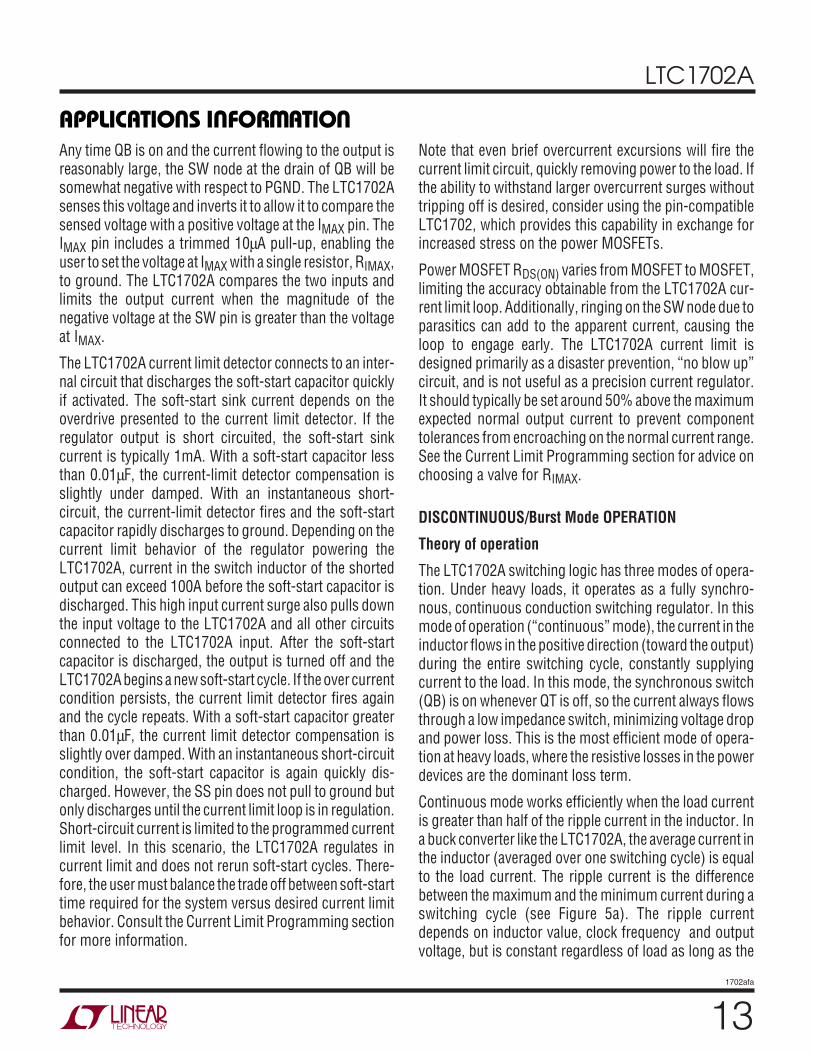
DISCONTINUOUS/Burst Mode OPERATION
Theory of operation
The LTC1702A switching logic has three modes of opera-tion. Under heavy loads, it operates as a fully synchro-nous, continuous conduction switching regulator. In thismode of operation (“continuous” mode), the current in theinductor flows in the positive direction (toward the output)during the entire switching cycle, constantly supplyingcurrent to the load. In this mode, the synchronous switch(QB) is on whenever QT is off, so the current always flowsthrough a low impedance switch, minimizing voltage dropand power loss. This is the most efficient mode of opera-tion at heavy loads, where the resistive losses in the powerdevices are the dominant loss term.
Continuous mode works efficiently when the load currentis greater than half of the ripple current in the inductor. Ina buck converter like the LTC1702A, the average current inthe inductor (averaged over one switching cycle) is equalto the load current. The ripple current is the differencebetween the maximum and the minimum current during aswitching cycle (see Figure 5a). The ripple currentdepends on inductor value, clock frequency and outputvoltage, but is constant regardless of load as long as the
14
LTC1702A
1702afa
LTC1702A remains in continuous mode. See the InductorSelection section for a detailed description of ripplecurrent.
As the output load current decreases in continuous mode,the average current in the inductor will reach a point whereit drops below half the ripple current. At this point, theinductor current will reverse during a portion of theswitching cycle, or begin to flow from the output back tothe input. This does not adversely affect regulation, butdoes cause additional losses as a portion of the inductorcurrent flows back and forth through the resistive powerswitches, giving away a little more power each time andlowering the efficiency. There are some benefits to allow-ing this reverse current flow: the circuit will maintainregulation even if the load current drops below zero (theload supplies current to the LTC1702A) and the outputripple voltage and frequency remain constant at all loads,easing filtering requirements. Circuits that take advantageof this behavior can force the LTC1702A to operate incontinuous mode at all loads by tying the FCB (ForceContinuous Bar) pin to ground.
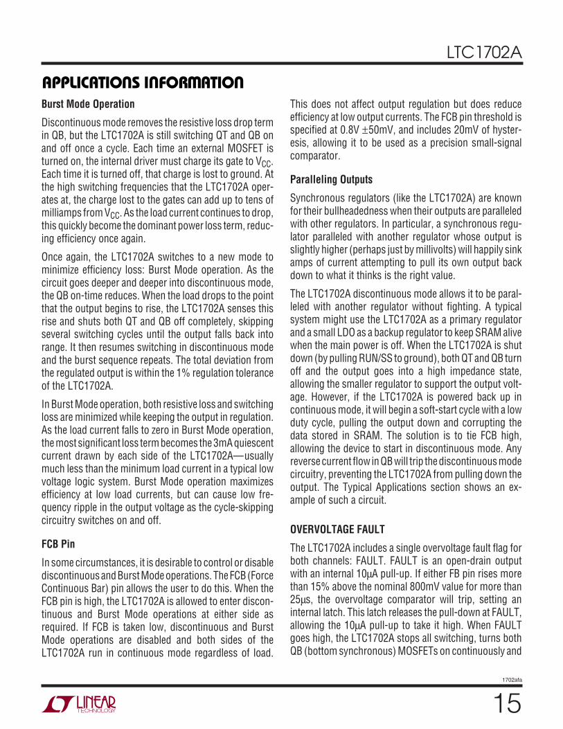
Discontinuous Mode
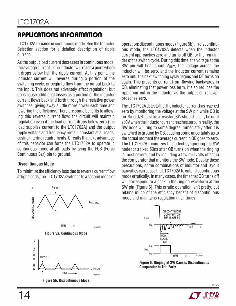
To minimize the efficiency loss due to reverse current flowat light loads, the LTC1702A switches to a second mode of
APPLICATIONS INFORMATION
WU UUFigure 6. Ringing at SW Causes DiscontinuousComparator to Trip Early
Figure 5a. Continuous Mode
Figure 5b. Discontinuous Mode
TIME
50nsBLANKTIME
0V
0V
5V
DISCONTINUOUSCOMPARATORTURNS OFF BGVSW
VBG
1702A F06TIME
operation: discontinuous mode (Figure 5b). In discontinu-ous mode, the LTC1702A detects when the inductorcurrent approaches zero and turns off QB for the remain-der of the switch cycle. During this time, the voltage at theSW pin will float about VOUT, the voltage across theinductor will be zero, and the inductor current remainszero until the next switching cycle begins and QT turns onagain. This prevents current from flowing backwards inQB, eliminating that power loss term. It also reduces theripple current in the inductor as the output current ap-proaches zero.
The LTC1702A detects that the inductor current has reachedzero by monitoring the voltage at the SW pin while QB ison. Since QB acts like a resistor, SW should ideally be rightat 0V when the inductor current reaches zero. In reality, theSW node will ring to some degree immediately after it isswitched to ground by QB, causing some uncertainty as tothe actual moment the average current in QB goes to zero.The LTC1702A minimizes this effect by ignoring the SWnode for a fixed 50ns after QB turns on when the ringingis most severe, and by including a few millivolts offset inthe comparator that monitors the SW node. Despite theseprecautions, some combinations of inductor and layoutparasitics can cause the LTC1702A to enter discontinuousmode erratically. In many cases, the time that QB turns offwill correspond to a peak in the ringing waveform at theSW pin (Figure 6). This erratic operation isn’t pretty, butretains much of the efficiency benefit of discontinuousmode and maintains regulation at all times.
TIME
IRIPPLE
IAVERAGE
INDU
CTOR
CUR
RENT
1702A F05a
TIME
IRIPPLE
IAVERAGEINDU
CTOR
CUR
RENT
1702A F05b
15
LTC1702A
1702afa
Burst Mode Operation
Discontinuous mode removes the resistive loss drop termin QB, but the LTC1702A is still switching QT and QB onand off once a cycle. Each time an external MOSFET isturned on, the internal driver must charge its gate to VCC.Each time it is turned off, that charge is lost to ground. Atthe high switching frequencies that the LTC1702A oper-ates at, the charge lost to the gates can add up to tens ofmilliamps from VCC. As the load current continues to drop,this quickly become the dominant power loss term, reduc-ing efficiency once again.
Once again, the LTC1702A switches to a new mode tominimize efficiency loss: Burst Mode operation. As thecircuit goes deeper and deeper into discontinuous mode,the QB on-time reduces. When the load drops to the pointthat the output begins to rise, the LTC1702A senses thisrise and shuts both QT and QB off completely, skippingseveral switching cycles until the output falls back intorange. It then resumes switching in discontinuous modeand the burst sequence repeats. The total deviation fromthe regulated output is within the 1% regulation toleranceof the LTC1702A.
In Burst Mode operation, both resistive loss and switchingloss are minimized while keeping the output in regulation.As the load current falls to zero in Burst Mode operation,the most significant loss term becomes the 3mA quiescentcurrent drawn by each side of the LTC1702A—usuallymuch less than the minimum load current in a typical lowvoltage logic system. Burst Mode operation maximizesefficiency at low load currents, but can cause low fre-quency ripple in the output voltage as the cycle-skippingcircuitry switches on and off.
FCB Pin
In some circumstances, it is desirable to control or disablediscontinuous and Burst Mode operations. The FCB (ForceContinuous Bar) pin allows the user to do this. When theFCB pin is high, the LTC1702A is allowed to enter discon-tinuous and Burst Mode operations at either side asrequired. If FCB is taken low, discontinuous and BurstMode operations are disabled and both sides of theLTC1702A run in continuous mode regardless of load.
APPLICATIONS INFORMATION
WU UU
This does not affect output regulation but does reduceefficiency at low output currents. The FCB pin threshold isspecified at 0.8V ±50mV, and includes 20mV of hyster-esis, allowing it to be used as a precision small-signalcomparator.
Paralleling Outputs
Synchronous regulators (like the LTC1702A) are knownfor their bullheadedness when their outputs are paralleledwith other regulators. In particular, a synchronous regu-lator paralleled with another regulator whose output isslightly higher (perhaps just by millivolts) will happily sinkamps of current attempting to pull its own output backdown to what it thinks is the right value.
The LTC1702A discontinuous mode allows it to be paral-leled with another regulator without fighting. A typicalsystem might use the LTC1702A as a primary regulatorand a small LDO as a backup regulator to keep SRAM alivewhen the main power is off. When the LTC1702A is shutdown (by pulling RUN/SS to ground), both QT and QB turnoff and the output goes into a high impedance state,allowing the smaller regulator to support the output volt-age. However, if the LTC1702A is powered back up incontinuous mode, it will begin a soft-start cycle with a lowduty cycle, pulling the output down and corrupting thedata stored in SRAM. The solution is to tie FCB high,allowing the device to start in discontinuous mode. Anyreverse current flow in QB will trip the discontinuous modecircuitry, preventing the LTC1702A from pulling down theoutput. The Typical Applications section shows an ex-ample of such a circuit.
OVERVOLTAGE FAULT
The LTC1702A includes a single overvoltage fault flag forboth channels: FAULT. FAULT is an open-drain outputwith an internal 10µA pull-up. If either FB pin rises morethan 15% above the nominal 800mV value for more than25µs, the overvoltage comparator will trip, setting aninternal latch. This latch releases the pull-down at FAULT,allowing the 10µA pull-up to take it high. When FAULTgoes high, the LTC1702A stops all switching, turns bothQB (bottom synchronous) MOSFETs on continuously and
16
LTC1702A
1702afa
remains in this state until both RUN/SS pins are pulled lowsimultaneously, the power supply is recycled, or theFAULT pin is pulled low externally. This behavior is in-tended to protect a potentially expensive load from over-voltage damage at all costs. Under some conditions, thisbehavior can cause the output voltage to undershootbelow ground. If latched FAULT mode is used, a Schottkydiode should be added with its cathode at the output andits anode at ground to clamp the negative voltage to a safelevel and prevent possible damage to the load and theoutput capacitors.
In some circuits, the OV latch can be a liability. Considera circuit where the output voltage at one channel may bechanged on the fly by switching in different feedbackresistors. A downward adjustment of greater than 15%will fire the fault latch, disabling both sides of the LTC1702Auntil the power is recycled. In circuits such as this, the faultlatch can be disabled by grounding the FAULT pin. Theinternal latch will still be set the first time the outputexceeds +15%, but the 10µA current source pull-up willnot be able to pull FAULT high, and the LTC1702A willignore the latch and continue normal operation. FAULTcan also be pulled down with external open-collector logicto restart a fault-latched LTC1702A as an alternative torecycling the power. Note that this will not reset theinternal latch; if the external pull-down is released, theLTC1702A will reenter FAULT mode. To reset the latch,pull both RUN/SS pins low simultaneously or cycle theinput power.
EXTERNAL COMPONENT SELECTION
POWER MOSFETs
Getting peak efficiency out of the LTC1702A dependsstrongly on the external MOSFETs used. The LTC1702Arequires at least two external MOSFETs per side—more ifone or more of the MOSFETs are paralleled to lower on-resistance. To work efficiently, these MOSFETs mustexhibit low RDS(ON) at 5V VGS (3.3V VGS if the PVCC inputsupply is 3.3V) to minimize resistive power loss while theyare conducting current. They must also have low gatecharge to minimize transition losses during switching. On
APPLICATIONS INFORMATION
WU UU
the other hand, voltage breakdown requirements in atypical LTC1702A circuit are pretty tame: the 7V maximuminput voltage limits the VDS and VGS the MOSFETs can seeto safe levels for most devices.
Low RDS(ON)
RDS(ON) calculations are pretty straightforward. RDS(ON) isthe resistance from the drain to the source of the MOSFETwhen the gate is fully on. Many MOSFETs have RDS(ON)specified at 4.5V gate drive—this is the right number touse in LTC1702A circuits running from a 5V supply. Ascurrent flows through this resistance while the MOSFET ison, it generates I2R watts of heat, where I is the currentflowing (usually equal to the output current) and R is theMOSFET RDS(ON). This heat is only generated when theMOSFET is on. When it is off, the current is zero and thepower lost is also zero (and the other MOSFET is busylosing power).
This lost power does two things: it subtracts from thepower available at the output, costing efficiency, and itmakes the MOSFET hotter—both bad things. The effect isworst at maximum load when the current in the MOSFETsand thus the power lost are at a maximum. LoweringRDS(ON) improves heavy load efficiency at the expense ofadditional gate charge (usually) and more cost (usually).Proper choice of MOSFET RDS(ON) becomes a trade-offbetween tolerable efficiency loss, power dissipation andcost. Note that while the lost power has a significant effecton system efficiency, it only adds up to a watt or two in atypical LTC1702A circuit, allowing the use of small, sur-face mount MOSFETs without heat sinks.
Gate Charge
Gate charge is amount of charge (essentially, the numberof electrons) that the LTC1702A needs to put into the gateof an external MOSFET to turn it on. The easiest way tovisualize gate charge is to think of it as a capacitance fromthe gate pin of the MOSFET to SW (for QT) or to PGND (forQB). This capacitance is composed of MOSFET channelcharge, actual parasitic drain-source capacitance and Miller-multiplied gate-drain capacitance, but can be approximatedas a single capacitance from gate to source. Regardless of

17
LTC1702A
1702afa
where the charge is going, the fact remains that it all hasto come out of VCC to turn the MOSFET gate on, and whenthe MOSFET is turned back off, that charge all ends up atground. In the meanwhile, it travels through the LTC1702A’sgate drivers, heating them up. More power lost!
In this case, the power is lost in little bite-sized chunks, onechunk per switch per cycle, with the size of the chunk setby the gate charge of the MOSFET. Every time the MOSFETswitches, another chunk is lost. Clearly, the faster theclock runs, the more important gate charge becomes as aloss term. Old-fashioned switchers that ran at 20kHz couldpretty much ignore gate charge as a loss term; in the550kHz LTC1702A, gate charge loss can be a significantefficiency penalty. Gate charge loss can be the dominantloss term at medium load currents, especially with largeMOSFETs. Gate charge loss is also the primary cause ofpower dissipation in the LTC1702A itself.
TG Charge Pump
There’s another nuance of MOSFET drive that the LTC1702Aneeds to get around. The LTC1702A is designed to use N-channel MOSFETs for both QT and QB, primarily becauseN-channel MOSFETs generally cost less and have lowerRDS(ON) than similar P-channel MOSFETs. Turning QB onis no big deal since the source of QB is attached to PGND;the LTC1702A just switches the BG pin between PGND andVCC. Driving QT is another matter. The source of QT isconnected to SW which rises to VCC when QT is on. Tokeep QT on, the LTC1702A must get TG one MOSFETVGS(ON) above VCC. It does this by utilizing a floating driverwith the negative lead of the driver attached to SW (thesource of QT) and the VCC lead of the driver coming outseparately at BOOST. An external 1µF capacitor CCP con-nected between SW and BOOST (Figure 2) supplies powerto BOOST when SW is high, and recharges itself throughDCP when SW is low. This simple charge pump keeps theTG driver alive even as it swings well above VCC. The valueof the bootstrap capacitor CCP needs to be at least 100times that of the total input capacitance of the topsideMOSFET(s). For very large external MOSFETs (or multipleMOSFETs in parallel), CCP may need to be increased overthe 1µF value.
APPLICATIONS INFORMATION
WU UU
MOSFET Gate Series Resistors
Traditional switching regulator designs often include re-sistors in series with the external MOSFET gates to controlgate rise and fall time, usually to control ringing at theswitching node. In LTC1702A applications, such resistorsprevent the onboard drivers from turning off the externalMOSFETs quickly, causing shoot through currents anderratic operation when both top and bottom MOSFETs areon simultaneously. Gate resistors are not recommendedin LTC1702A applications. In some cases, long PCB tracescan add enough impedance to the gate to hinder turn off.Keep gate traces as short and wide as practical.
Switch node ringing can be reduced by adding a low valueresistor (usually 5Ω to 10Ω) in series with the BOOST pin.This will slow TG rise time without affecting MOSFET turnoff, allowing the LTC1702A to keep shoot through currentunder control. This resistor will typically improve thewaveform at the switch node but it reduces efficiency andincreases power dissipation in the top MOSFET. Use withcaution.
INPUT SUPPLY
The BiCMOS process that allows the LTC1702A to includelarge MOSFET drivers on-chip also limits the maximuminput voltage to 7V. This limits the practical maximuminput supply to a loosely regulated 5V or 6V rail. TheLTC1702A will operate properly with input supplies downto about 3V, so a typical 3.3V supply can also be used if theexternal MOSFETs are chosen appropriately (see the PowerMOSFETs section).
At the same time, the input supply needs to supply severalamps of current without excessive voltage drop. The inputsupply must have regulation adequate to prevent suddenload changes from causing the LTC1702A input voltage todip. In most typical applications where the LTC1702A isgenerating a secondary low voltage logic supply, all ofthese input conditions are met by the main system logicsupply when fortified with an input bypass capacitor.
Input Bypass
A typical LTC1702A circuit running from a 5V logic supplymight provide 1.6V at 10A at one of its outputs. 5V to 1.6V
18
LTC1702A
1702afa
APPLICATIONS INFORMATION
WU UU
Calculating RMS Current in CIN
A buck regulator like the LTC1702A draws pulses ofcurrent from the input capacitor during normal opera-tion. The input capacitor sees this as AC current, anddissipates power proportional to the RMS value of theinput current waveform. To properly specify the capaci-tor, we need to know the RMS value of the input current.Calculating the approximate RMS value of a pulse trainwith a fixed duty cycle is straightforward, but theLTC1702A complicates matters by running two sidessimultaneously and out of phase, creating a complexwaveform at the input.
To calculate the approximate RMS value of the inputcurrent, we first need to calculate the average DC valuewith both sides of the LTC1702A operating at maximumload. Over a single period, the system will spend sometime with one top switch on and the other off, perhapssome time with both switches on, and perhaps sometime with both switches off. During the time each topswitch is on, the current will equal that side’s full loadoutput current. When both switches are on, the totalcurrent will be the sum of the two full load currents, andwhen both are off, the current is effectively zero. Multiplyeach current value by the percentage of the period thatthe current condition lasts, and sum the results—this isthe average DC current value.
As an example, consider a circuit that takes a 5V inputand generates 3.3V at 3A at side 1 and 1.6V at 10A atside 2. When a cycle starts, TG1 turns on and 3A flows
TIME0 A B C D
50% 16% 16% 18%
IAVE
0
INPU
T CU
RREN
T (A
)
5.2
3
10
13
1702A SB1
Figure SB1. Average Current Calculation
implies a duty cycle of 32%, which means QT is on 32%of each switching cycle. During QT’s on-time, the currentdrawn from the input equals the load current and duringthe rest of the cycle, the current drawn from the input isnear zero. This 0A to 10A, 32% duty cycle pulse train addsup to 4.7ARMS at the input. At 550kHz, switching cycleslast about 1.8µs—most system logic supplies have nohope of regulating output current with that kind of speed.A local input bypass capacitor is required to make up thedifference and prevent the input supply from droppingdrastically when QT kicks on. This capacitor is usuallychosen for RMS ripple current capability and ESR as wellas value.
The input bypass capacitor in an LTC1702A circuit iscommon to both channels. Consider our 10A examplecase with the other side of the LTC1702A disabled. Theinput bypass capacitor gets exercised in three ways: itsESR must be low enough to keep the initial drop as QTturns on within reason (100mV or so); its RMS currentcapability must be adequate to withstand the 4.6ARMSripple current at the input and the capacitance must belarge enough to maintain the input voltage until the inputsupply can make up the difference. Generally, a capacitorthat meets the first two parameters will have far morecapacitance than is required to keep capacitance-baseddroop under control. In our example, we need 0.01Ω ESRto keep the input drop under 100mV with a 10A currentstep and 4.6ARMS ripple current capacity to avoid over-heating the capacitor. These requirements can be met withmultiple low ESR tantalum or electrolytic capacitors inparallel, or with a large monolithic ceramic capacitor.
The two sides of the LTC1702A run off a single masterclock and are wired 180° out of phase with each other tosignificantly reduce the total capacitance/ESR needed atthe input. Assuming 100mV of ripple and 10A outputcurrent, we needed an ESR of 0.01Ω and 4.7A ripplecurrent capability for one side. Now, assume both sidesare running simultaneously with identical loading. If thetwo sides switched in phase, all the loading conditionswould double and we’d need enough capacitance for9.4ARMS and 0.005Ω ESR. With the two sides out ofphase, the input current is 4.8ARMS—barely larger thanthe single case (Figure 7)! The peak current deltas are stillonly 10A, requiring the same 0.01Ω ESR rating. As long as
19
LTC1702A
1702afa
APPLICATIONS INFORMATION
WU UU
from CIN (time point A). 50% of the way through, TG2turns on and the total current is 13A (time point B).Shortly thereafter, TG1 turns off and the current drops to10A (time point C). Finally, TG2 turns off and the currentspends a short time at 0 before TG1 turns on again (timepoint D).
I A A
A A A
AVG =( )+( )+
( )+( )=
3 0 5 13 0 16
10 0 16 0 0 18 5 18
• . • .
• . • . .
Now we can calculate the RMS current. Using the samewaveform we used to calculate the average DC current,subtract the average current from each of the DC values.Square each current term and multiply the squares by thesame period percentages we used to calculate the aver-age DC current. Sum the results and take the square root.The result is the approximate RMS current as seen by theinput capacitor with both sides of the LTC1702A at fullload. Actual RMS current will differ due to inductor ripplecurrent and resistive losses, but this approximate value isadequate for input capacitor calculation purposes.
TIME0 A B C D
50% 16% 16% 18%
–5.2
AC IN
PUT
CURR
ENT
(A)
0
–2.2
4.8
7.8
1702A SB2
Figure SB2. AC Current Calculation
I
A
RMS
RMS
=( )+( )+
( )+( )=
– . • . . • .
. • . – . • .
.
2 18 0 5 7 82 0 16
4 82 0 16 5 18 0 18
4 55
2 2
2 2
If the circuit is likely to spend time with one side operatingand the other side shut down, the RMS current will needto be calculated for each possible case (side 1 on, side 2off; side 1 off, side 2 on; both sides on). The capacitormust be sized to withstand the largest RMS current of thethree—sometimes this occurs with one side shut down!
Side only
I A A A
I A
Side only
I A A A
I
AVE
RMS RMS
AVE
RMS
1
3 0 67 0 0 33 2 01
1 0 67 2 0 33 1 42
2
10 0 32 0 0 68 3 2
6 8 0 32 3 2 0 68
1
12 2
2
22 2
:
• . • . .
• . – • . .
:
• . • . .
. • . – . • .
=( )+( )=
= ( )+( )=
=( )+( )=
= ( )+( )=44 66 4 55. .A ARMS RMS>
Consider the case where both sides are operating at thesame load, with a 50% duty cycle at each side. The RMScurrent with both sides running is near zero, while theRMS current with one side active is 1/2 the total loadcurrent of that side. The 2-phase, 5V to 2.5V circuit in theapplications section takes advantage of this phenom-enon, allowing it to supply 40A of output current with only120µF of input capacitance (and only 40µF of outputcapacitance!).
the capacitor we chose for the single side application cansupport the slightly higher 4.8ARMS current, we can addthe second channel without changing the input capacitorat all. As a general rule, an input bypass capacitor capableof supporting the larger output current channel can sup-port both channels running simultaneously (see the2-Phase Operation section for more details).
Tantalum capacitors are a popular choice as input capaci-tors for LTC1702A applications, but they deserve a special
caution here. Generic tantalum capacitors have a destruc-tive failure mechanism when they are subjected to largeRMS currents (like those seen at the input of a LTC1702A).At some random time after they are turned on, they canblow up for no apparent reason. The capacitor manufac-turers are aware of this and sell special “surge tested”tantalum capacitors specifically designed for use withswitching regulators. When choosing a tantalum inputcapacitor, make sure that it is rated to carry the RMS
20
LTC1702A
1702afa
current that the LTC1702A will draw. If the data sheetdoesn’t give an RMS current rating, chances are thecapacitor isn’t surge tested. Don’t use it!
OUTPUT BYPASS CAPACITOR
The output bypass capacitor has quite different require-ments from the input capacitor. The ripple current at theoutput of a buck regulator like the LTC1702A is muchlower than at the input, due to the fact that the inductorcurrent is constantly flowing at the output whenever theLTC1702A is operating in continuous mode. The primaryconcern at the output is capacitor ESR. Fast load currenttransitions at the output will appear as voltage across theESR of the output bypass capacitor until the feedback loopin the LTC1702A can change the inductor current to matchthe new load current value. This ESR step at the output isoften the single largest budget item in the load regulationcalculation. As an example, our hypothetical 1.6V, 10Aswitcher with a 0.01Ω ESR output capacitor would expe-rience a 100mV step at the output with a 0 to 10A loadstep—a 6.3% output change!
Usually the solution is to parallel several capacitors at theoutput. For example, to keep the transient response insideof 3% with the previous design, we’d need an output ESRbetter than 0.0048Ω. This can be met with three 0.014Ω,470µF low ESR tantalum capacitors in parallel.
APPLICATIONS INFORMATION
WU UU
INDUCTOR
The inductor in a typical LTC1702A circuit is chosenprimarily for value and saturation current. The inductorvalue sets the ripple current, which is commonly chosenat around 40% of the anticipated full load current. Ripplecurrent is set by:
It V
LRIPPLEON Q OUT= ( )( )2
In our hypothetical 1.6V, 10A example, we'd set the ripplecurrent to 40% of 10A or 4A, and the inductor value wouldbe:
Lt V
Is VA
H
with tV
VkHz s
ON Q OUT
RIPPLE
ON Q
= ( ) =µ( )( ) = µ
= −⎛⎝⎜
⎞⎠⎟
= µ
( )
( )
. ..
./ .
2
2
1 2 1 64
0 5
11 65
550 1 2
The inductor must not saturate at the expected peakcurrent. In this case, if the current limit was set to 15A, theinductor should be rated to withstand 15A + 1/2 IRIPPLE,or 17A without saturating.
FEEDBACK LOOP/COMPENSATION1
Feedback Loop Types
In a typical LTC1702A circuit, the feedback loop consistsof the modulator, the external inductor and output capaci-tor, and the feedback amplifier and its compensationnetwork. All of these components affect loop behavior andneed to be accounted for in the loop compensation. Themodulator consists of the internal PWM generator, theoutput MOSFET drivers and the external MOSFETs them-selves. From a feedback loop point of view, it looks like alinear voltage transfer function from COMP to SW and hasa gain roughly equal to the input voltage. It has fairlybenign AC behavior at typical loop compensation frequen-cies with significant phase shift appearing at half theswitching frequency.
The external inductor/output capacitor combination makesa more significant contribution to loop behavior. Thesecomponents cause a second order LC roll-off at the1The information in this section is based on the paper “The K Factor: A New Mathematical Tool forStability Analysis and Synthesis” by H. Dean Venable, Venable Industries, Inc. For complete paper,see “Reference Reading #4” at www.linear-tech.com.
0
10A32%
68%
0
10A32% 18%
18%
18%32%
–3.2A0
6.8A32%
68%
Q1 CURRENT, SIDE 1 ONLY(FOR 1-PHASE, 2 SIDES:MULTIPLY CURRENT BY 2)
CURRENT IN CIN, SIDE 1 ONLYICIN = 4.66ARMS, (1-PHASE,2 SIDES: ICIN = 9.3ARMS)
CURRENT IN CIN, BOTH SIDES EQUAL LOADICIN = 4.8ARMS
Q11 CURRENTQ21 CURRENT
BOTH SIDES EQUAL LOAD2-PHASE OPERATION
–6.4A
03.6A
32% 18%
1702A F07
32%
Figure 7. RMS Input Current
21
LTC1702A
1702afa
APPLICATIONS INFORMATION
WU UU
output, with the attendant 180° phase shift. This roll-off iswhat filters the PWM waveform, resulting in the desiredDC output voltage, but the phase shift complicates theloop compensation if the gain is still higher than unity atthe pole frequency. Eventually (usually well above the LCpole frequency), the reactance of the output capacitor willapproach its ESR, and the roll-off due to the capacitor willstop, leaving 6dB/octave and 90° of phase shift (Figure 8).
OUTIN
R1
C2
C1R2
RB
1702A F10aVREF
+
–
GAIN(dB)
PHASE(DEG)
1702A F10b
0 0
–90
–180
–270
PHASE
GAIN
–6dB/OCT
–6dB/OCT
Figure 10a. Type 2 Amplifier Schematic Diagram
Figure 10b. Type 2 Amplifier Transfer Function
So far, the AC response of the loop is pretty well out of theuser’s control. The modulator is a fundamental piece of theLTC1702A design, and the external L and C are usuallychosen based on the regulation and load current require-ments without considering the AC loop response. Thefeedback amplifier, on the other hand, gives us a handlewith which to adjust the AC response. The goal is to have180° phase shift at DC (so the loop regulates) and some-thing less than 360° phase shift at the point that the loopgain falls to 0dB. The simplest strategy is to set up thefeedback amplifier as an inverting integrator, with the 0dBfrequency lower than the LC pole (Figure 9). This “type 1”configuration is stable but transient response will be lessthan exceptional if the LC pole is at a low frequency.
Figure 10 shows an improved “type 2” circuit that uses anadditional pole-zero pair to temporarily remove 90° ofphase shift. This allows the loop to remain stable with 90°more phase shift in the LC section, provided the loopreaches 0dB gain near the center of the phase “bump.”
GAIN(dB)
PHASE(DEG)
1702A F08
AV
0 0
–90
–180–6dB/OCT
PHASE
GAIN
–12dB/OCT
Figure 8. Transfer Function of Buck Modulator
OUTIN
R1
C1
RB
1702A F09aVREF
+
–
GAIN(dB)
PHASE(DEG)
1702A F09b
0 0
–90
–180
–270
GAIN
PHASE
–6dB/OCT
Figure 9a. Type 1 Amplifier Schematic Diagram
Figure 9b. Type 1 Amplifier Transfer Function
22
LTC1702A
1702afa
tors need type 3 compensation to obtain acceptable phasemargin with a high bandwidth feedback loop.
Feedback Component Selection
Selecting the R and C values for a typical type 2 or type 3loop is a nontrivial task. The applications shown in this datasheet show typical values, optimized for the power com-ponents shown. They should give acceptable performancewith similar power components, but can be way off if evenone major power component is changed significantly.Applications that require optimized transient response willneed to recalculate the compensation values specificallyfor the circuit in question. The underlying mathematics arecomplex, but the component values can be calculated in astraightforward manner if we know the gain and phase ofthe modulator at the crossover frequency.
Modulator gain and phase can be measured directly froma breadboard, or can be simulated if the appropriateparasitic values are known. Measurement will give moreaccurate results, but simulation can often get close enoughto give a working system. To measure the modulator gainand phase directly, wire up a breadboard with an LTC1702Aand the actual MOSFETs, inductor, and input and outputcapacitors that the final design will use. This breadboardshould use appropriate construction techniques for highspeed analog circuitry: bypass capacitors located close tothe LTC1702A, no long wires connecting components,appropriately sized ground returns, etc. Wire the feedbackamplifier as a simple type 1 loop, with a 10k resistor fromVOUT to FB and a 0.1µF feedback capacitor from COMP toFB. Choose the bias resistor (RB) as required to set thedesired output voltage. Disconnect RB from ground andconnect it to a signal generator or to the source output ofa network analyzer (Figure 12) to inject a test signal intothe loop. Measure the gain and phase from the COMP pinto the output node at the positive terminal of the outputcapacitor. Make sure the analyzer’s input is AC coupled sothat the DC voltages present at both the COMP and VOUTnodes don’t corrupt the measurements or damage theanalyzer.
Type 2 loops work well in systems where the ESR zero inthe LC roll-off happens close to the LC pole, limiting thetotal phase shift due to the LC. The additional phasecompensation in the feedback amplifier allows the 0dBpoint to be at or above the LC pole frequency, improvingloop bandwidth substantially over a simple type 1 loop. Ithas limited ability to compensate for LC combinationswhere low capacitor ESR keeps the phase shift near 180°for an extended frequency range. LTC1702A circuits usingconventional switching grade electrolytic output capaci-tors can often get acceptable phase margin with type 2compensation.
“Type 3” loops (Figure 11) use two poles and two zeros toobtain a 180° phase boost in the middle of the frequencyband. A properly designed type 3 circuit can maintainacceptable loop stability even when low output capacitorESR causes the LC section to approach 180° phase shiftwell above the initial LC roll-off. As with a type 2 circuit, theloop should cross through 0dB in the middle of the phasebump to maximize phase margin. Many LTC1702A cir-cuits using low ESR tantalum or OS-CON output capaci-
APPLICATIONS INFORMATION
WU UU
OUTIN
R1
R3
C2
C1C3
R2
RB
1702A F11aVREF
+
–
GAIN(dB)
PHASE(DEG)
1702A F11b
0 0
–90
–180
–270
+6dB/OCT–6dB/OCT
PHASE
GAIN
–6dB/OCT
Figure 11a. Type 3 Amplifier Schematic Diagram
Figure 11B. Type 3 Amplifier Transfer Function
23
LTC1702A
1702afa
With the gain/phase plot in hand, a loop crossover fre-quency can be chosen. Usually the curves look somethinglike Figure 8. Choose the crossover frequency in the risingor flat parts of the phase curve, beyond the external LCpoles. Frequencies between 10kHz and 50kHz usuallywork well. Note the gain (GAIN, in dB) and phase (PHASE,in degrees) at this point. The desired feedback amplifiergain will be –GAIN to make the loop gain 0dB at thisfrequency. Now calculate the needed phase boost, assum-ing 60° as a target phase margin:
BOOST = – (PHASE + 30°)
If the required BOOST is less than 60°, a type 2 loop canbe used successfully, saving two external components.BOOST values greater than 60° usually require type 3loops for satisfactory performance.
Finally, choose a convenient resistor value for R1 (10k isusually a good value). Now calculate the remaining values:
(K is a constant used in the calculations)
ƒ = chosen crossover frequency
G = 10(GAIN/20) (this converts GAIN in dB to G in absolutegain)
Type 2 Loop:
K TanBOOST
CGKR
C C K
RK
C
RV R
V VB
REF
OUT REF
= + °⎛
⎝⎜⎞
⎠⎟
=πƒ
= ( )=
πƒ
=( )
245
21
2 1
1 2 1
22 1
1
2 –
–
APPLICATIONS INFORMATION
WU UU
If breadboard measurement is not practical, a SPICEsimulation can be used to generate approximate gain/phase curves. Plug the expected capacitor, inductor andMOSFET values into the following SPICE deck and gener-ate an AC plot of V(VOUT)/V(COMP) in dB and phase ofV(OUT) in degrees. Refer to your SPICE manual for detailsof how to generate this plot.*1702A modulator gain/phase*©2001 Linear Technology*this file written to run with PSpice 8.0*may require modifications for other SPICEsimulators
*MOSFETsrfet mod sw 0.02 ;MOSFET rdson
*inductorlext sw out1 1u ;inductor valuerl out1 out 0.005 ;inductor series R
*output capcout out out2 1000u ;capacitor valueresr out2 0 0.01 ;capacitor ESR
*1702A internalsemod mod 0 comp 0 5 ;3.3 for 3.3V supplyvstim comp 0 0 ac 1 ;ac stimulus.ac dec 100 1k 1meg.probe.end
BOOST2
TG
SW
BG
FCB
FAULT
COMP
FB
RUN/SS
1/2 LTC1702A
VCC
10Ω MBR0530TCIN
5V
QT1µF
VOUTTO ANALYZER
VCOMPTO
ANALYZER
ACSOURCE
FROMANALYZER
LEXT
QB
10µF
0.1µF
RB
PVCC
SGND PGND
+
+
10k
NCCOUT
1702A F12
+
Figure 12. Modulator Gain/Phase Measurement Set-Up
24
LTC1702A
1702afa
chosen properly. The CF term is an approximate factor thatcorrects for errors caused by ringing on the switch node(illustrated in Figure 6). This correction factor will changedepending on the layout and the components used, but–10mV is usually a good starting point. However, toprovide adequate margin and to accommodate for offsetsand external variations, it is recommended that VPROG becalculated with CF = –10 ± 50mV. VPROG is then pro-grammed at the IMAX pin using the internal 10µA pull-upand an external resistor:
RILIM = VPROG/10µA
The resulting value of RILIM should be checked in an actualcircuit to ensure that the ILIM circuit kicks in as expected.MOSFET RDS(ON) specs are like horsepower ratings inautomobiles, and should be taken with a grain of salt.Circuits that use very low values for RIMAX (<10k) shouldbe checked carefully, since small changes in RIMAX cancause large ILIM changes. If VPROG is set too low, theLTC1702A may fail to start up.
Accuracy Trade-Offs
The VDS sensing scheme used in the LTC1702A is notparticularly accurate, primarily due to uncertainty in theRDS(ON) from MOSFET to MOSFET. A second error termarises from the ringing present at the SW pin, whichcauses the VDS to look larger than (ILOAD)(RDS(ON)) at thebeginning of QB’s on-time. These inaccuracies do notprevent the LTC1702A current limit circuit from protectingitself and the load from damaging overcurrent conditions,but they do prevent the user from setting the current limitto a tight tolerance if more than one copy of the circuit isbeing built. The 50% factor in the current setting equationabove reflects the margin necessary to ensure that thecircuit will stay out of current limit at the maximum normalload, even with a hot MOSFET that is running quite a bithigher than its RDS(ON) spec.
FCB OPERATION/SECONDARY WINDINGS
The FCB pin can be used in conjunction with a secondarywinding on one side of the LTC1702A to generate a thirdregulated voltage output. This output can be directlyregulated at the FCB pin. In theory, a fourth output could
APPLICATIONS INFORMATION
WU UU
Type 3 Loop:
K TanBOOST
CGR
C C K
RKC
RR
K
CK R
RV R
V VB
REF
OUT REF
= + °⎛
⎝⎜⎞
⎠⎟
=πƒ
= ( )=
πƒ
= ( )=
πƒ
=( )
24
45
21
2 11 2 1
22 1
31
1
31
2 3
1
–
–
–
CURRENT LIMIT PROGRAMMING
Programming the current limit on the LTC1702A is straight-forward. The IMAX pin sets the current limit by setting themaximum allowable voltage drop across QB (the bottomMOSFET) before the current limit circuit engages. Thevoltage across QB is set by its on-resistance and thecurrent flowing in the inductor, which is the same as theoutput current. The LTC1702A current limit circuit invertsthe voltage at IMAX before comparing it with the negativevoltage across QB, allowing the current limit to be set witha positive voltage.
To set the current limit, calculate the expected voltage dropacross QB at the maximum desired current:
V I R CFPROG LIM DS ON= ( )( ) +( )
ILIM should be chosen to be quite a bit higher than theexpected operating current, to allow for MOSFET RDS(ON)changes with temperature. Setting ILIM to 150% of themaximum normal operating current is usually safe and willadequately protect the power components if they are
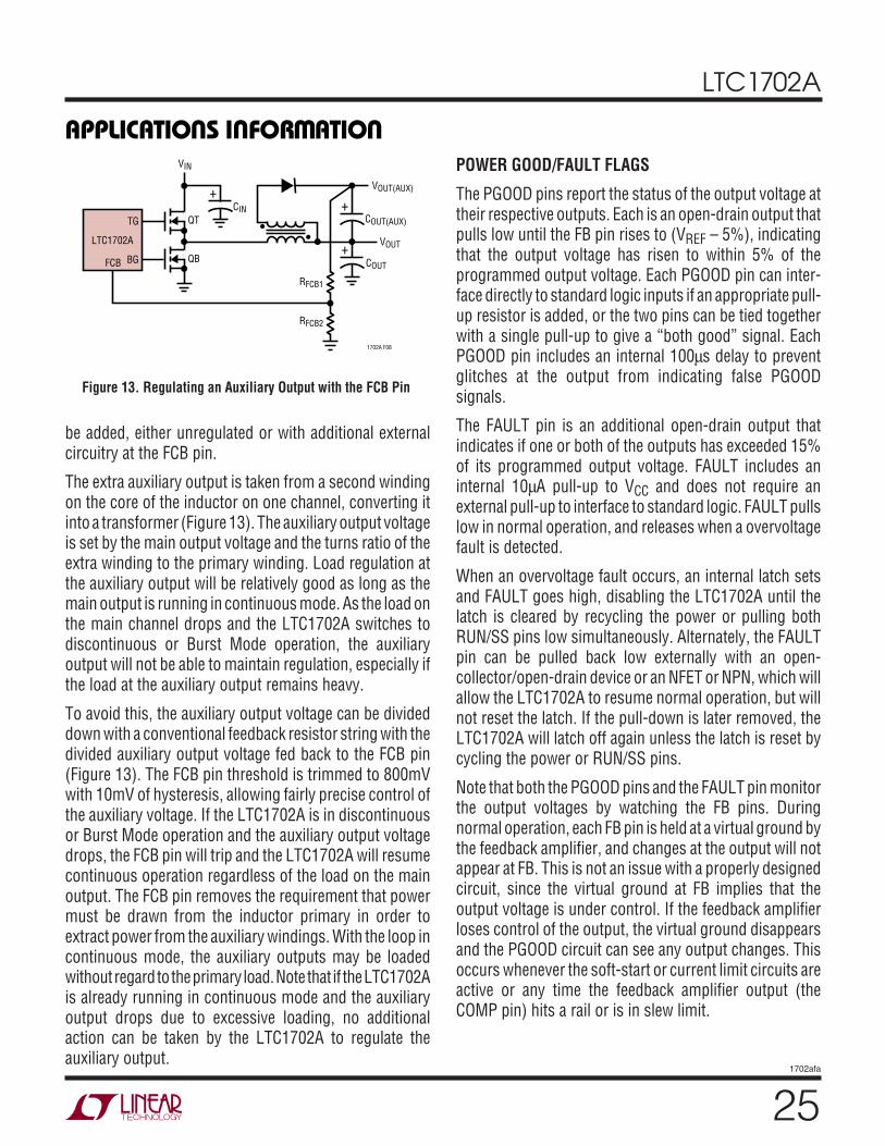
25
LTC1702A
1702afa
POWER GOOD/FAULT FLAGS
The PGOOD pins report the status of the output voltage attheir respective outputs. Each is an open-drain output thatpulls low until the FB pin rises to (VREF – 5%), indicatingthat the output voltage has risen to within 5% of theprogrammed output voltage. Each PGOOD pin can inter-face directly to standard logic inputs if an appropriate pull-up resistor is added, or the two pins can be tied togetherwith a single pull-up to give a “both good” signal. EachPGOOD pin includes an internal 100µs delay to preventglitches at the output from indicating false PGOODsignals.
The FAULT pin is an additional open-drain output thatindicates if one or both of the outputs has exceeded 15%of its programmed output voltage. FAULT includes aninternal 10µA pull-up to VCC and does not require anexternal pull-up to interface to standard logic. FAULT pullslow in normal operation, and releases when a overvoltagefault is detected.
When an overvoltage fault occurs, an internal latch setsand FAULT goes high, disabling the LTC1702A until thelatch is cleared by recycling the power or pulling bothRUN/SS pins low simultaneously. Alternately, the FAULTpin can be pulled back low externally with an open-collector/open-drain device or an NFET or NPN, which willallow the LTC1702A to resume normal operation, but willnot reset the latch. If the pull-down is later removed, theLTC1702A will latch off again unless the latch is reset bycycling the power or RUN/SS pins.
Note that both the PGOOD pins and the FAULT pin monitorthe output voltages by watching the FB pins. Duringnormal operation, each FB pin is held at a virtual ground bythe feedback amplifier, and changes at the output will notappear at FB. This is not an issue with a properly designedcircuit, since the virtual ground at FB implies that theoutput voltage is under control. If the feedback amplifierloses control of the output, the virtual ground disappearsand the PGOOD circuit can see any output changes. Thisoccurs whenever the soft-start or current limit circuits areactive or any time the feedback amplifier output (theCOMP pin) hits a rail or is in slew limit.
APPLICATIONS INFORMATION
WU UU
be added, either unregulated or with additional externalcircuitry at the FCB pin.
The extra auxiliary output is taken from a second windingon the core of the inductor on one channel, converting itinto a transformer (Figure 13). The auxiliary output voltageis set by the main output voltage and the turns ratio of theextra winding to the primary winding. Load regulation atthe auxiliary output will be relatively good as long as themain output is running in continuous mode. As the load onthe main channel drops and the LTC1702A switches todiscontinuous or Burst Mode operation, the auxiliaryoutput will not be able to maintain regulation, especially ifthe load at the auxiliary output remains heavy.
To avoid this, the auxiliary output voltage can be divideddown with a conventional feedback resistor string with thedivided auxiliary output voltage fed back to the FCB pin(Figure 13). The FCB pin threshold is trimmed to 800mVwith 10mV of hysteresis, allowing fairly precise control ofthe auxiliary voltage. If the LTC1702A is in discontinuousor Burst Mode operation and the auxiliary output voltagedrops, the FCB pin will trip and the LTC1702A will resumecontinuous operation regardless of the load on the mainoutput. The FCB pin removes the requirement that powermust be drawn from the inductor primary in order toextract power from the auxiliary windings. With the loop incontinuous mode, the auxiliary outputs may be loadedwithout regard to the primary load. Note that if the LTC1702Ais already running in continuous mode and the auxiliaryoutput drops due to excessive loading, no additionalaction can be taken by the LTC1702A to regulate theauxiliary output.
Figure 13. Regulating an Auxiliary Output with the FCB Pin
+
TG
LTC1702A
BGFCB COUT
RFCB1
+COUT(AUX)
VOUT(AUX)
1702A F08
+CIN
QT
QB
VOUT
VIN
RFCB2
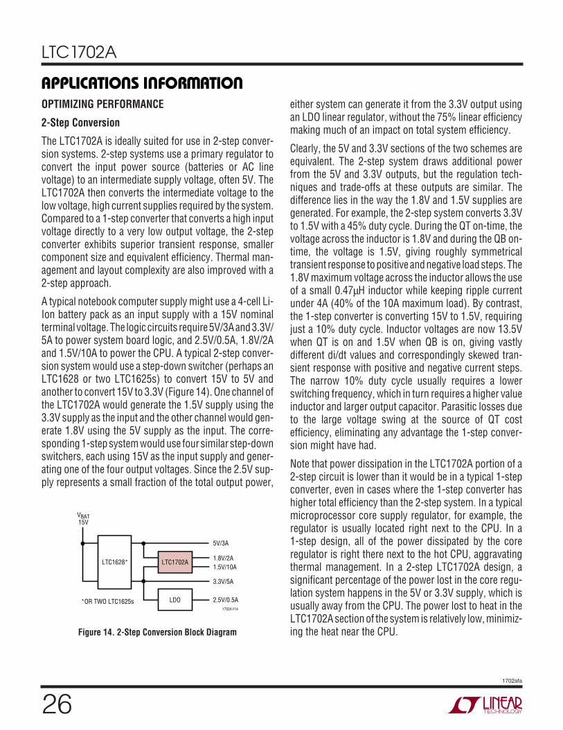
26
LTC1702A
1702afa
OPTIMIZING PERFORMANCE
2-Step Conversion
The LTC1702A is ideally suited for use in 2-step conver-sion systems. 2-step systems use a primary regulator toconvert the input power source (batteries or AC linevoltage) to an intermediate supply voltage, often 5V. TheLTC1702A then converts the intermediate voltage to thelow voltage, high current supplies required by the system.Compared to a 1-step converter that converts a high inputvoltage directly to a very low output voltage, the 2-stepconverter exhibits superior transient response, smallercomponent size and equivalent efficiency. Thermal man-agement and layout complexity are also improved with a2-step approach.
A typical notebook computer supply might use a 4-cell Li-Ion battery pack as an input supply with a 15V nominalterminal voltage. The logic circuits require 5V/3A and 3.3V/5A to power system board logic, and 2.5V/0.5A, 1.8V/2Aand 1.5V/10A to power the CPU. A typical 2-step conver-sion system would use a step-down switcher (perhaps anLTC1628 or two LTC1625s) to convert 15V to 5V andanother to convert 15V to 3.3V (Figure 14). One channel ofthe LTC1702A would generate the 1.5V supply using the3.3V supply as the input and the other channel would gen-erate 1.8V using the 5V supply as the input. The corre-sponding 1-step system would use four similar step-downswitchers, each using 15V as the input supply and gener-ating one of the four output voltages. Since the 2.5V sup-ply represents a small fraction of the total output power,
APPLICATIONS INFORMATION
WU UU
either system can generate it from the 3.3V output usingan LDO linear regulator, without the 75% linear efficiencymaking much of an impact on total system efficiency.
Clearly, the 5V and 3.3V sections of the two schemes areequivalent. The 2-step system draws additional powerfrom the 5V and 3.3V outputs, but the regulation tech-niques and trade-offs at these outputs are similar. Thedifference lies in the way the 1.8V and 1.5V supplies aregenerated. For example, the 2-step system converts 3.3Vto 1.5V with a 45% duty cycle. During the QT on-time, thevoltage across the inductor is 1.8V and during the QB on-time, the voltage is 1.5V, giving roughly symmetricaltransient response to positive and negative load steps. The1.8V maximum voltage across the inductor allows the useof a small 0.47µH inductor while keeping ripple currentunder 4A (40% of the 10A maximum load). By contrast,the 1-step converter is converting 15V to 1.5V, requiringjust a 10% duty cycle. Inductor voltages are now 13.5Vwhen QT is on and 1.5V when QB is on, giving vastlydifferent di/dt values and correspondingly skewed tran-sient response with positive and negative current steps.The narrow 10% duty cycle usually requires a lowerswitching frequency, which in turn requires a higher valueinductor and larger output capacitor. Parasitic losses dueto the large voltage swing at the source of QT costefficiency, eliminating any advantage the 1-step conver-sion might have had.
Note that power dissipation in the LTC1702A portion of a2-step circuit is lower than it would be in a typical 1-stepconverter, even in cases where the 1-step converter hashigher total efficiency than the 2-step system. In a typicalmicroprocessor core supply regulator, for example, theregulator is usually located right next to the CPU. In a1-step design, all of the power dissipated by the coreregulator is right there next to the hot CPU, aggravatingthermal management. In a 2-step LTC1702A design, asignificant percentage of the power lost in the core regu-lation system happens in the 5V or 3.3V supply, which isusually away from the CPU. The power lost to heat in theLTC1702A section of the system is relatively low, minimiz-ing the heat near the CPU.Figure 14. 2-Step Conversion Block Diagram
VBAT15V
LTC1628*
*OR TWO LTC1625s
LTC1702A
LDO
5V/3A
1.8V/2A1.5V/10A
3.3V/5A
2.5V/0.5A1702A F14

27
LTC1702A
1702afa
2-Step Efficiency Calculation
Calculating the efficiency of a 2-step converter systeminvolves some subtleties. Simply multiplying the effi-ciency of the primary 5V or 3.3V supply by the efficiencyof the 1.8V or 1.5V supply underestimates the actualefficiency, since a significant fraction of the total power isdrawn from the 3.3V and 5V rails in a typical system. Thecorrect way to calculate system efficiency is to calculatethe power lost in each stage of the converter, and dividethe total output power from all outputs by the sum of theoutput power plus the power lost:
EfficiencyTotalOutputPower
TotalOutputPower TotalPowerLost
=
+( )100%
In our example 2-step system, the total output power is:
Total output power =15W + 16.5W + 1.25W + 3.6W + 15W = 51.35Wcorresponding to 5V, 3.3V, 2.5V, 1.8V and 1.5V outputvoltages.
Assuming the LTC1702A provides 90% efficiency at eachoutput, the additional load on the 5V and 3.3V supplies is:
1.5V: 15W/90% = 16.6W/3.3V = 5A from 3.3V1.8V: 3.6W/90% = 4W/5V = 0.8A from 5V2.5V: 1.25W/75% = 1.66W/3.3V = 0.5A from 3.3V
If the 5V and 3.3V supplies are each 94% efficient, thepower lost in each supply is:
1.5V: 17.55W – 15W = 2.55W1.8V: 4.26W – 3.6W = 0.66W2.5V: 1.77W – 1.25W = 0.52W3.3V: 17.55W – 16.5W = 1.05W5V: 15.96W – 15W = 0.96W
Total loss = 5.74W
Total system efficiency =51.35W/(51.35W + 5.74W) = 90%
APPLICATIONS INFORMATION
WU UU
Maximizing High Load Current Efficiency
Efficiency at high load currents (when the LTC1702A isoperating in continuous mode) is primarily controlled bythe resistance of the components in the power path (QT,QB, LEXT) and power lost in the gate drive circuits due toMOSFET gate charge. Maximizing efficiency in this regionof operation is as simple as minimizing these terms.
The behavior of the load over time affects the efficiencystrategy. Parasitic resistances in the MOSFETs and theinductor set the maximum output current the circuit cansupply without burning up. A typical efficiency curve(Figure 15) shows that peak efficiency occurs near 30% ofthis maximum current. If the load current will vary aroundthe efficiency peak and will spend relatively little time at themaximum load, choosing components so that the averageload is at the efficiency peak is a good idea. This puts themaximum load well beyond the efficiency peak, but usu-ally gives the greatest system efficiency over time, whichtranslates to the longest run time in a battery-poweredsystem. If the load is expected to be relatively constant atthe maximum level, the components should be chosen sothat this load lands at the peak efficiency point, well belowthe maximum possible output of the converter.
Figure 15. Typical LTC1702A Efficiency Curves
LOAD CURRENT (A)0
70
EFFI
CIEN
CY (%
)
80
90
100
5 10
1702A G01
15
VIN = 5VVOUT = 3.3V
VOUT = 2.5V
VOUT = 1.6V
28
LTC1702A
1702afa
Maximizing Low Load Current Efficiency
Low load current efficiency depends strongly on properoperation in discontinuous and Burst Mode operations. Inan ideally optimized system, discontinuous mode reducesconduction losses but not switching losses, since eachpower MOSFET still switches on and off once per cycle. Ina typical system, there is additional loss in discontinuousmode due to a small amount of residual current left in theinductor when QB turns off. This current gets dissipatedacross the body diode of either QT or QB. Some LTC1702Asystems lose as much to body diode conduction as theysave in MOSFET conduction. The real efficiency benefit ofdiscontinuous mode happens when Burst Mode operationis invoked. At typical power levels, when Burst Modeoperation is activated, gate drive is the dominant lossterm. Burst Mode operation turns off all output switchingfor several clock cycles in a row, significantly cutting gatedrive losses. As the load current in Burst Mode operationfalls toward zero, the current drawn by the circuit falls tothe LTC1702A’s background quiescent level—about 3mAper channel.
To maximize low load efficiency, make sure the LTC1702Ais allowed to enter discontinuous and Burst Mode opera-tion as cleanly as possible. FCB must be above its 0.8Vthreshold. Minimize ringing at the SW node so that thediscontinuous comparator leaves as little residual currentin the inductor as possible when QB turns off. It helps toconnect the SW pin of the LTC1702A as close to the drainof QB as possible. An RC snubber network can also beadded from SW to PGND.
REGULATION OVER COMPONENT TOLERANCE/TEMPERATURE
DC Regulation Accuracy
The LTC1702A initial DC output accuracy depends mainlyon internal reference accuracy, op amp offset and externalresistor accuracy. Two LTC1702A specs come into play:feedback voltage and feedback voltage line regulation. Thefeedback voltage spec is 800mV ± 8mV over the fulltemperature range, and is specified at the FB pin, whichencompasses both reference accuracy and any op amp
offset. This accounts for 1% error at the output with a 5Vinput supply. The feedback voltage line regulation specadds an additional 0.05%/V term that accounts for changein reference output with change in input supply voltage.With a 5V supply, the errors contributed by the LTC1702Aitself add up to no more than 1% DC error at the output.
The output voltage setting resistors (R1 and RB inFigure 3) are the other major contributor to DC error. At atypical 1.xV output voltage, the resistors are of roughly thesame value, which tends to halve their error terms, im-proving accuracy. Still, using 1% resistors for R1 and RBwill add 1% to the total output error budget, equal to thatof all errors due to the LTC1702A combined. Using 0.1%resistors in just those two positions can nearly halve theDC output error for very little additional cost.
Load Regulation
Load regulation is affected by feedback voltage, feedbackamplifier gain and external ground drops in the feedbackpath. Feedback voltage is covered above and is within 1%over temperature. A full-range load step might require a10% duty cycle change to keep the output constant,requiring the COMP pin to move about 100mV. Withamplifier gain at 85dB, this adds up to only a 10µV shift atFB, negligible compared to the reference accuracy terms.
External ground drops aren’t so negligible. The LTC1702Acan sense the positive end of the output voltage byattaching the feedback resistor directly at the load, but itcannot do the same with the ground lead. Just 0.001Ω ofresistance in the ground lead at 10A load will cause a 10mVerror in the output voltage—as much as all the other DCerrors put together. Proper layout becomes essential toachieving optimum load regulation from the LTC1702A.See the Layout/Troubleshooting section for more infor-mation. A properly laid out LTC1702A circuit should moveless than a millivolt at the output from zero to full load.
TRANSIENT RESPONSE
Transient response is the other half of the regulationequation. The LTC1702A can keep the DC output voltageconstant to within 1% when averaged over hundreds of
APPLICATIONS INFORMATION
WU UU
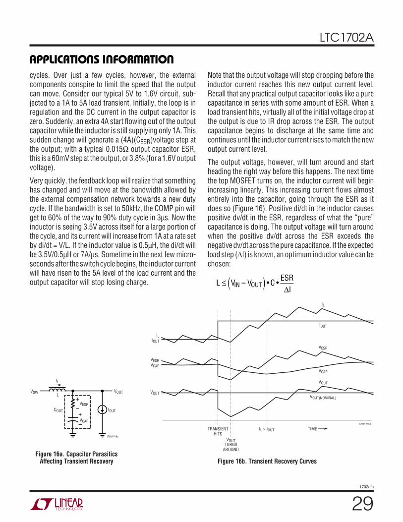
29
LTC1702A
1702afa
cycles. Over just a few cycles, however, the externalcomponents conspire to limit the speed that the outputcan move. Consider our typical 5V to 1.6V circuit, sub-jected to a 1A to 5A load transient. Initially, the loop is inregulation and the DC current in the output capacitor iszero. Suddenly, an extra 4A start flowing out of the outputcapacitor while the inductor is still supplying only 1A. Thissudden change will generate a (4A)(CESR)voltage step atthe output; with a typical 0.015Ω output capacitor ESR,this is a 60mV step at the output, or 3.8% (for a 1.6V outputvoltage).
Very quickly, the feedback loop will realize that somethinghas changed and will move at the bandwidth allowed bythe external compensation network towards a new dutycycle. If the bandwidth is set to 50kHz, the COMP pin willget to 60% of the way to 90% duty cycle in 3µs. Now theinductor is seeing 3.5V across itself for a large portion ofthe cycle, and its current will increase from 1A at a rate setby di/dt = V/L. If the inductor value is 0.5µH, the di/dt willbe 3.5V/0.5µH or 7A/µs. Sometime in the next few micro-seconds after the switch cycle begins, the inductor currentwill have risen to the 5A level of the load current and theoutput capacitor will stop losing charge.
Note that the output voltage will stop dropping before theinductor current reaches this new output current level.Recall that any practical output capacitor looks like a purecapacitance in series with some amount of ESR. When aload transient hits, virtually all of the initial voltage drop atthe output is due to IR drop across the ESR. The outputcapacitance begins to discharge at the same time andcontinues until the inductor current rises to match the newoutput current level.
The output voltage, however, will turn around and startheading the right way before this happens. The next timethe top MOSFET turns on, the inductor current will beginincreasing linearly. This increasing current flows almostentirely into the capacitor, going through the ESR as itdoes so (Figure 16). Positive di/dt in the inductor causespositive dv/dt in the ESR, regardless of what the “pure”capacitance is doing. The output voltage will turn aroundwhen the positive dv/dt across the ESR exceeds thenegative dv/dt across the pure capacitance. If the expectedload step (∆I) is known, an optimum inductor value can bechosen:
L V V CESR
IIN OUT≤ ( ) ∆
– • •
APPLICATIONS INFORMATION
WU UU
+
–
–
IL
VOUT
IOUT
1702A F16a
VESRCOUT
VCAP
VSW L+
VCAP
VOUT
TRANSIENTHITS
VOUTTURNS
AROUND
IL > IOUT TIME
VESR
IOUT
IL
VOUT
VESR
IOUT
IL
VCAP
VOUT(NOMINAL)
1702A F16b
Figure 16b. Transient Recovery CurvesFigure 16a. Capacitor Parasitics
Affecting Transient Recovery
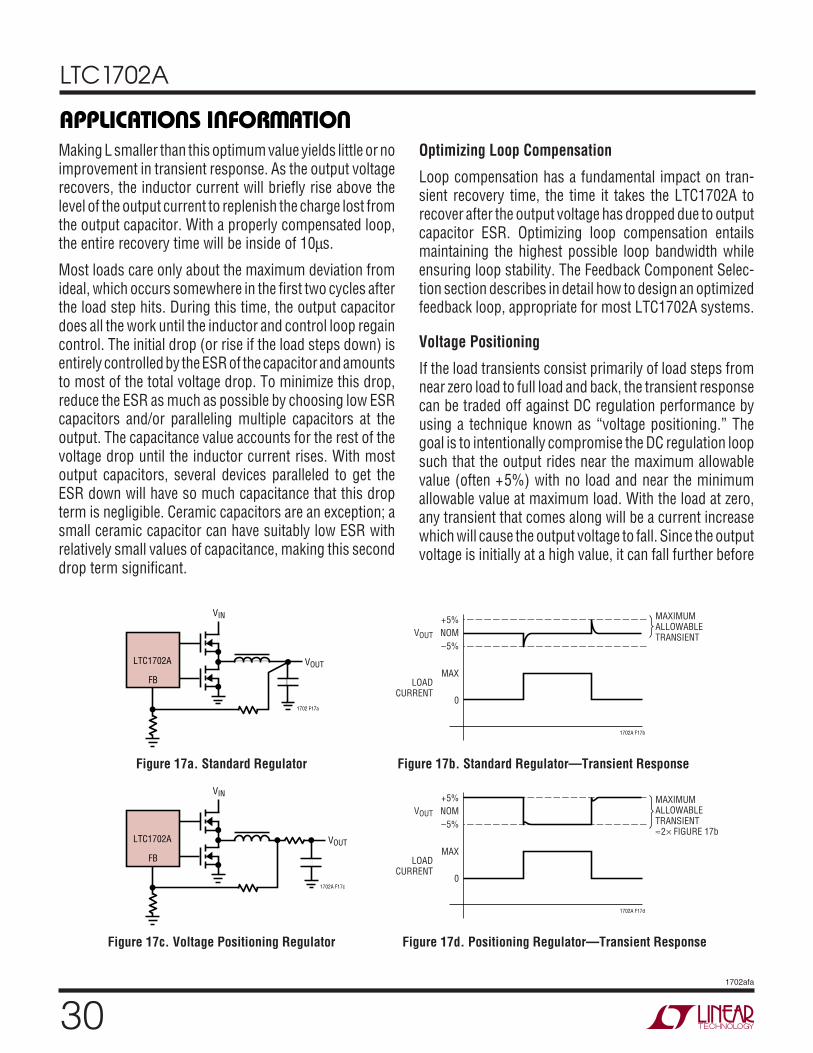
30
LTC1702A
1702afa
APPLICATIONS INFORMATION
WU UU
Making L smaller than this optimum value yields little or noimprovement in transient response. As the output voltagerecovers, the inductor current will briefly rise above thelevel of the output current to replenish the charge lost fromthe output capacitor. With a properly compensated loop,the entire recovery time will be inside of 10µs.
Most loads care only about the maximum deviation fromideal, which occurs somewhere in the first two cycles afterthe load step hits. During this time, the output capacitordoes all the work until the inductor and control loop regaincontrol. The initial drop (or rise if the load steps down) isentirely controlled by the ESR of the capacitor and amountsto most of the total voltage drop. To minimize this drop,reduce the ESR as much as possible by choosing low ESRcapacitors and/or paralleling multiple capacitors at theoutput. The capacitance value accounts for the rest of thevoltage drop until the inductor current rises. With mostoutput capacitors, several devices paralleled to get theESR down will have so much capacitance that this dropterm is negligible. Ceramic capacitors are an exception; asmall ceramic capacitor can have suitably low ESR withrelatively small values of capacitance, making this seconddrop term significant.
Optimizing Loop Compensation
Loop compensation has a fundamental impact on tran-sient recovery time, the time it takes the LTC1702A torecover after the output voltage has dropped due to outputcapacitor ESR. Optimizing loop compensation entailsmaintaining the highest possible loop bandwidth whileensuring loop stability. The Feedback Component Selec-tion section describes in detail how to design an optimizedfeedback loop, appropriate for most LTC1702A systems.
Voltage Positioning
If the load transients consist primarily of load steps fromnear zero load to full load and back, the transient responsecan be traded off against DC regulation performance byusing a technique known as “voltage positioning.” Thegoal is to intentionally compromise the DC regulation loopsuch that the output rides near the maximum allowablevalue (often +5%) with no load and near the minimumallowable value at maximum load. With the load at zero,any transient that comes along will be a current increasewhich will cause the output voltage to fall. Since the outputvoltage is initially at a high value, it can fall further before
LTC1702A
FB
1702 F17a
1702A F17b
VOUT
VIN +5%
–5%NOM
MAX
0
VOUT
LOADCURRENT
MAXIMUMALLOWABLETRANSIENT
Figure 17a. Standard Regulator Figure 17b. Standard Regulator—Transient Response
LTC1702A
FB
1702A F17c
1702A F17d
VOUT
VIN +5%
–5%NOM
MAX
0
VOUT
LOADCURRENT
Figure 17c. Voltage Positioning Regulator Figure 17d. Positioning Regulator—Transient Response
MAXIMUMALLOWABLETRANSIENT≈2× FIGURE 17b

31
LTC1702A
1702afa
it goes out of spec. Similarly, at full load, the output currentcan only decrease, causing a positive shift in the outputvoltage; the initial low value allows it to rise further beforethe spec is exceeded. The primary benefit of voltagepositioning is it increases the allowable ESR of the outputcapacitors, saving cost. An additional bonus is that atmaximum load, the output voltage is near the minimumallowable, decreasing the power dissipated in the load.
Implementing voltage positioning is as simple as creatingan intentional resistance in the output path to generate therequired voltage drop. This resistance can be a low valueresistor, a length of PCB trace, or even the parasiticresistance of the inductor if an appropriate filter is used. Ifthe LTC1702A senses the output voltage upstream fromthe resistance (Figure 17), the output voltage will movewith load as I • R, where I is the load current and R is thevalue of the resistance. If the feedback network is thenreset to regulate near the upper edge of the specifiedtolerance, the output voltage will ride high when ILOAD islow and will ride low when ILOAD is high. Compared to atraditional regulator, a voltage positioning regulator cantheoretically stand as much as twice the ESR drop acrossthe output capacitor while maintaining output voltageregulation. This means smaller, cheaper output capacitorscan be used while keeping the output voltage withinacceptable limits.
Measurement Techniques
Measuring transient response presents a challenge intwo respects: obtaining an accurate measurement andgenerating a suitable transient to use to test the circuit.Output measurements should be taken with a scopeprobedirectly across the output capacitor. Proper highfrequency probing techniques should be used. In particu-lar, don’t use the 6" ground lead that comes with theprobe! Use an adapter that fits on the tip of the probe andhas a short ground clip to ensure that inductance in theground path doesn’t cause a bigger spike than the tran-sient signal being measured. Conveniently, the typicalprobe tip ground clip is spaced just right to span the leadsof a typical output capacitor. In general, it is best to take
this measurement with the 20MHz bandwidth limit on theoscilloscope turned on to limit high frequency noise. Notethat microprocessor manufacturers typically specify ripple≤20MHz, as energy above 20MHz is generally radiatedand not conducted and will not affect the load even if itappears at the output capacitor.
Now that we know how to measure the signal, we need tohave something to measure. The ideal situation is to usethe actual load for the test, and switch it on and off whilewatching the output. If this isn’t convenient, a current stepgenerator is needed. This generator needs to be able toturn on and off in nanoseconds to simulate a typicalswitching logic load, so stray inductance and long clipleads between the LTC1702A and the transient generatormust be minimized.
Figure 18 shows an example of a simple transient genera-tor. Be sure to use a noninductive resistor as the loadelement—many power resistors use an inductive spiralpattern and are not suitable for use here. A simple solutionis to take ten 1/4W film resistors and wire them in parallelto get the desired value. This gives a noninductive resistiveload which can dissipate 2.5W continuously or 50W ifpulsed with a 5% duty cycle, enough for most LTC1702Acircuits. Solder the MOSFET and the resistor(s) as close tothe output of the LTC1702A circuit as possible and set upthe signal generator to pulse at a 100Hz rate with a 5% dutycycle. This pulses the LTC1702A with 500µs transients10ms apart, adequate for viewing the entire transientrecovery time for both positive and negative transitionswhile keeping the load resistor cool.
APPLICATIONS INFORMATION
WU UUFigure 18. Transient Load Generator
LTC1702A
PULSEGENERATOR
1702A F18
IRFZ44 OREQUIVALENT
50Ω
0V TO 10V100Hz, 5%
DUTY CYCLE
VOUT
RLOAD
LOCATE CLOSETO THE OUTPUT

32
LTC1702A
1702afa
APPLICATIONS INFORMATION
WU UU
FAULT BEHAVIOR
Changing the Output Voltage on the Fly
Some applications use a switching scheme attached to thefeedback resistors to allow the system to adjust theLTC1702A output voltage. The voltage can be changed onthe fly if desired, but care must be taken to avoid trippingthe overvoltage fault circuit. Stepping the voltage upwardsabruptly is safe, but stepping down quickly by more than15% can leave the system in a state where the outputvoltage is still at the old higher level, but the feedback nodeis set to expect a new, substantially lower voltage. If thiscondition persists for more than 10µs, the overvoltagefault circuitry will fire and latch off the LTC1702A.
The simplest solution is to disable the fault circuit bygrounding the FAULT pin. Systems that must keep thefault circuit active should ensure that the output voltage is
TYPICAL APPLICATIONSU
3.3VIN, 2.5V/1.8V Output Power Supply
LTC1702A
PVCC
BOOST1
BG1
TG1
SW1
IMAX1
PGOOD1
FCB
RUN/SS
COMP1
SGND
FB1
IMAX2
BOOST2
BG2
TG2
SW2
PGND
PGOOD2
FAULT
RUN/SS2
COMP2
FB2
VCC
C51µF
R110Ω
C61µFC8
1µF
R2 28.7k
R825.5k
R102.4k
R9 27k
1702A TA02
R34.3k
R410k1%
C11820pF
C920pF
C10100pF
R7 68k
C151µF
VOUT21.8V12A
C7 1µF
R58.06k1%10k
Q2A
Q2B
Q1B Q1AD3
D2D1, D2: MOTOROLA MBR0520LT1D3: MOTOROLA MBRS320T3C1: KEMET T510X477M006ASC12, C20: PANASONIC EEFUE0G181RL1: SUMIDA CEP1254712-T007L2: SUMIDA CDRH744734-JPS023Q1A, Q1B, Q2A, Q2B: SILICONIX Si9804Q3, Q4: 1/2 SILICONIX Si4966
D1
GND
L10.68µH
C12180µF
×3
C410µF
C31µF
C21µF
C16 1µF
C1470µF×2
+
Q3
Q4
C191000pF
C17100pF
C181000pF
R1210.7k
1%
R134.99k
1%
L21µH
C20180µF
C211µF
VOUT12.5V5A
GNDVINVIN
FAULTPGOOD2
VIN3.3V ± 5%
++
PGOOD1
10k
never programmed to step down by more than 15% in anysingle step. The safest strategy is to step the output downby 10% or less at a time and wait for the output to settleto the new value before taking subsequent steps.
VID Applications
Certain microprocessors specify a set of codes that corre-spond to power supply voltages required from the regula-tor system. If these codes are changed on the fly, the samecaveats as above apply. In addition, the switching matrixthat programs the output voltage may vary its resistancesignificantly over the entire span of output voltages,potentially changing the loop compensation if the circuit isnot designed properly. With a typical type 3 feedback loop(Figure 3), make sure that the RB resistor is modified to setthe output voltage. The R1 resistor must stay constant toensure that the loop compensation is not affected.
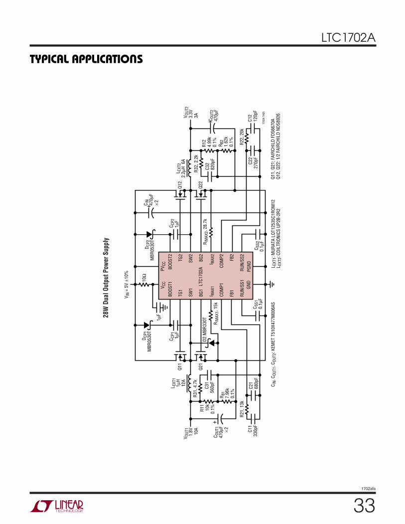
33
LTC1702A
1702afa
TYPICAL APPLICATIONS
U
BOOS
T1
TG1
SW1
BG1
I MAX
1
COM
P1
FB1
RUN/
SS1
BOOS
T2 TG2
SW2
BG2
I MAX
2
COM
P2 FB2
RUN/
SS2
LTC1
702A
V CC
PVCC
GND
PGND
+
+
+
V OUT
11.
8V 10A
C OUT
147
0µF
× 2
R11
10k
0.1%
C11
330p
F
R B1
7.96
k0.
1%
C21
680p
F
C31
560p
F
L EXT
11µ
H12
AL E
XT2
2.2µ
H 6
A
R31,
4.7
k
R21,
13k
Q11
Q21
D CP2
MBR
0530
T
D CP1
MBR
0530
T
C CP1 1µF
C CP2
1µF
D2 M
BR33
0T1µF
R IM
AX1,
15k C S
S10.
1µF
C SS2
0.1µ
F
10Ω
C I
N47
0µF
× 2
Q12
Q22
V OUT
23.
3V3A
C OUT
247
0µF
C12
120p
FC2
227
0pF
R22,
20k
1702
A TA
05
R B2
1.62
k0.
1%
R12
4.99
k0.
1%
C32
820p
F
R32,
2.2
k
Q11,
Q21
: FAI
RCHI
LD F
DS66
70A
Q12,
Q22
: 1/2
FAI
RCHI
LD N
DS89
26C I
N, C
OUT1
, COU
T2: K
EMET
T51
0X47
7M00
6AS
R IM
AX2,
28.
7k
V IN
= 5V
±10
%
L EXT
1: M
URAT
A LQ
T125
35C1
ROM
12L E
XT2:
COI
LTRO
NICS
UP2
B-2R
2
28W
Dua
l Out
put P
ower
Sup
ply
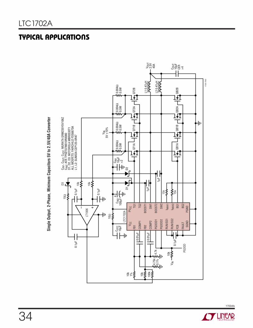
34
LTC1702A
1702afa
TYPICAL APPLICATIONS
U
Sing
le O
utpu
t, 2-
Phas
e, M
inim
um C
apac
itors
5V
to 2
.5V/
40A
Conv
erte
r
QT1A
C IN1
10µF
×2
D1D2
1µF
QT1B
QT2A
QT2B
0.00
4Ω0.
5W0.
004Ω
0.5W
V IN
5V ±
10%
0.00
4Ω0.
5W0.
004Ω
0.5W
C IN1
, COU
T, C
VCC:
MUR
ATA
GRM
235Y
5V10
6ZC I
N2: A
VX T
PSD1
07M
010R
0080
D1, D
2, D
3: M
OTOR
OLA
MBR
0530
T1AL
L M
OSFE
TS: F
AIRC
HILD
FDS
6670
AL1
, L2:
SUM
IDA
CEP1
25-0
R47
C IN2
100µ
F
+
V CC
PVCC
LTC1
702A
1702
A TA
03
10Ω
10k
10k
10Ω
D3
SGND
PGND
FB1
COM
P1
FB2
COM
P2
PGOO
D1
PGOO
D2
RUN/
SS1
RUN/
SS2
FCB
FAUL
T
TG1
TG2
BOOS
T1
SW1
BOOS
T2
SW2
I MAX
1
I MAX
2
BG1
BG2
C VCC
10µF
0.01
µF
0.01
µF
4.7k
10k
10k
10k
1% 100k
4.75
k0.
1%
0.1µ
F
0.1µ
F
0.1µ
F
1µF
0.1µ
FV I
N
QB1A
QB1B
QB2A
QB2B
L2 0
.47µ
H
L1 0
.47µ
H
– +
LT10
06
15k
15k
PGOO
D
C OUT
10µF
CER
×4V OUT
2.5V
40A
35
LTC1702A
1702afa
PACKAGE DESCRIPTION
U
Information furnished by Linear Technology Corporation is believed to be accurate and reliable.However, no responsibility is assumed for its use. Linear Technology Corporation makes no represen-tation that the interconnection of its circuits as described herein will not infringe on existing patent rights.
GN Package24-Lead Plastic SSOP (Narrow .150 Inch)
(Reference LTC DWG # 05-08-1641)
.337 – .344*(8.560 – 8.738)
GN24 (SSOP) 0204
1 2 3 4 5 6 7 8 9 10 11 12
.229 – .244(5.817 – 6.198)
.150 – .157**(3.810 – 3.988)
161718192021222324 15 1413
.016 – .050(0.406 – 1.270)
.015 ± .004(0.38 ± 0.10)
× 45°
0° – 8° TYP.0075 – .0098(0.19 – 0.25)
.0532 – .0688(1.35 – 1.75)
.008 – .012(0.203 – 0.305)
TYP
.004 – .0098(0.102 – 0.249)
.0250(0.635)
BSC
.033(0.838)
REF
.254 MIN
RECOMMENDED SOLDER PAD LAYOUT
.150 – .165
.0250 BSC.0165 ± .0015
.045 ±.005
*DIMENSION DOES NOT INCLUDE MOLD FLASH. MOLD FLASH SHALL NOT EXCEED 0.006" (0.152mm) PER SIDE**DIMENSION DOES NOT INCLUDE INTERLEAD FLASH. INTERLEAD FLASH SHALL NOT EXCEED 0.010" (0.254mm) PER SIDE
INCHES(MILLIMETERS)
NOTE:1. CONTROLLING DIMENSION: INCHES
2. DIMENSIONS ARE IN
3. DRAWING NOT TO SCALE
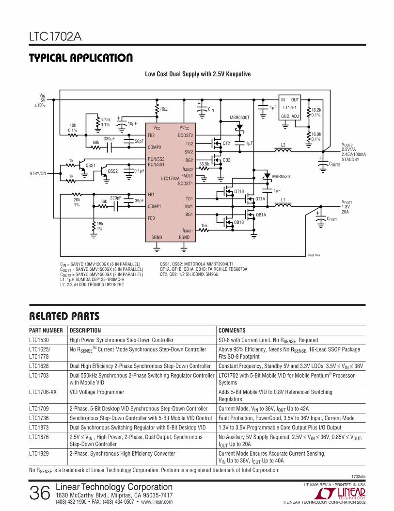
36
LTC1702A
1702afa
LT 0306 REV A • PRINTED IN USA
© LINEAR TECHNOLOGY CORPORATION 2002
Linear Technology Corporation1630 McCarthy Blvd., Milpitas, CA 95035-7417(408) 432-1900 FAX: (408) 434-0507 www.linear.com
TYPICAL APPLICATION
U
RELATED PARTSPART NUMBER DESCRIPTION COMMENTS
LTC1530 High Power Synchronous Step-Down Controller SO-8 with Current Limit. No RSENSE Required
LTC1625/ No RSENSETM Current Mode Synchronous Step-Down Controller Above 95% Efficiency, Needs No RSENSE, 16-Lead SSOP Package
LTC1778 Fits SO-8 Footprint
LTC1628 Dual High Efficiency 2-Phase Synchronous Step-Down Controller Constant Frequency, Standby 5V and 3.3V LDOs, 3.5V ≤ VIN ≤ 36V
LTC1703 Dual 550kHz Synchronous 2-Phase Switching Regulator Controller LTC1702 with 5-Bit Mobile VID for Mobile Pentium® Processorwith Mobile VID Systems
LTC1706-XX VID Voltage Programmer Adds 5-Bit Mobile VID to 0.8V Referenced SwitchingRegulators
LTC1709 2-Phase, 5-Bit Desktop VID Synchronous Step-Down Controller Current Mode, VIN to 36V, IOUT Up to 42A
LTC1736 Synchronous Step-Down Controller with 5-Bit Mobile VID Control Fault Protection, PowerGood, 3.5V to 36V Input, Current Mode
LTC1873 Dual Synchronous Switching Regulator with 5-Bit Desktop VID 1.3V to 3.5V Programmable Core Output Plus I/O Output
LTC1876 2.5V ≤ VIN , High Power, 2-Phase, Dual Output, Synchronous No Auxiliary 5V Supply Required, 2.5V ≤ VIN ≤ 36V, 0.85V ≤ VOUT,Step-Down Controller IOUT Up to 20A
LTC1929 2-Phase, Synchronous High Efficiency Converter Current Mode Ensures Accurate Current Sensing,VIN Up to 36V, IOUT Up to 40A
No RSENSE is a trademark of Linear Technology Corporation. Pentium is a registered trademark of Intel Corporation.
Low Cost Dual Supply with 2.5V Keepalive
+
FB2
COMP2
RUN/SS2
FB1
COMP1
FCB
BOOST2
TG2
SW2
BG2
IMAX2
VCC PVCC
SGND PGND
LTC1702A
4.75k0.1%
0.1µF
39pF
56pF
220pF
330pF
56k20k1%
16k1%
QSS2QSS1
CIN = SANYO 10MV1200GX (6 IN PARALLEL)COUT1 = SANYO 6MV1500GX (8 IN PARALLEL)COUT2 = SANYO 6MV1500GX (3 IN PARALLEL)L1: 1µH SUMIDA CEP125-1R0MC-HL2: 2.2µH COILTRONICS UP2B-2R2
VIN5V
±10%
STBY/ON
1k
68k
1k
10k0.1%
36.5k
QT2
MBR0530T
1µF
QB2
QT1A
QT1B
MBR0530T
1µF
COUT1
1702A TA04
+COUT2
+10µF
+CIN
1µF
16.9k0.1%
16.2k0.1%
VOUT22.5V/7A2.45V/100mASTANDBY
VOUT11.8V20A
10Ω
L1
QB1A
QB1B15k
FAULT
BOOST1
TG1
SW1
BG1
IMAX1
L2
IN OUT
GND
LT1761
ADJ
RUN/SS1
QSS1, QSS2: MOTOROLA MMBT3904LT1QT1A, QT1B, QB1A, QB1B: FAIRCHILD FDS6670AQT2, QB2: 1/2 SILICONIX Si4966