ltc2452 - ultra-tiny, differential, 16-bit ΔΣ adc with …€¦ · ultra-tiny, differential,...
TRANSCRIPT

LTC2452
12452fd
For more information www.linear.com/LTC2452
Typical applicaTion
FeaTures
applicaTions
DescripTion
Ultra-Tiny, Differential, 16-Bit ∆Σ ADC with SPI Interface
The LTC®2452 is an ultra-tiny, fully differential, 16-bit, analog-to-digital converter. The LTC2452 uses a single 2.7V to 5.5V supply and communicates through an SPI interface. The ADC is available in an 8-pin, 3mm × 2mm DFN package or TSOT-23 package. It includes an integrated oscillator that does not require any external components. It uses a delta-sigma modulator as a converter core and has no latency for multiplexed applications. The LTC2452 includes a proprietary input sampling scheme that reduces the average input sampling current several orders of magnitude when compared to conventional delta-sigma converters. Additionally, due to its architecture, there is negligible current leakage between the input pins.
The LTC2452 can sample at 60 conversions per second, and due to the very large oversampling ratio, has extremely relaxed anti-aliasing requirements. The LTC2452 includes continuous internal offset and full-scale calibration algo-rithms which are transparent to the user, ensuring accuracy over time and over the operating temperature range. The converter has an external REF pin and the differential input voltage range can extend up to ±VREF .
Following a single conversion, the LTC2452 can automati-cally enter a sleep mode and reduce its supply current to less than 0.2µA. If the user reads the ADC once a second, the LTC2452 consumes an average of less than 50µW from a 2.7V supply.
Integral Nonlinearity, VCC = 3V
n ±VCC Differential Input Rangen 16-Bit Resolution (Including Sign), No Missing
Codesn 2LSB Offset Errorn 4LSB Full-Scale Errorn 60 Conversions Per Secondn Single Conversion Settling Time for Multiplexed
Applicationsn Single-Cycle Operation with Auto Shutdownn 800µA Supply Currentn 0.2µA Sleep Currentn Internal Oscillator—No External Components
Requiredn SPI Interfacen Ultra-Tiny 3mm × 2mm DFN and TSOT-23 Packages
n System Monitoringn Environmental Monitoringn Direct Temperature Measurementsn Instrumentationn Industrial Process Controln Data Acquisitionn Embedded ADC UpgradesL, LT, LTC, LTM, Linear Technology and the Linear logo are registered trademarks and No Latency ∆Σ is a trademark of Linear Technology Corporation. All other trademarks are the property of their respective owners. Protected by U.S. Patents, including 6208279, 6411242, 7088280, 7164378.
DIFFERENTIAL INPUT VOLTAGE (V)–3
INL
(LSB
)
1
3
2452 TA01b
–1
0
2
–2
–3–1–2 1 20 3
TA = –45°C, 25°C, 90°C
10k
10k
10k
R
CS
3-WIRE SPIINTERFACE
SCK
SDO
0.1µF
0.1µF 10µF
2.7V TO 5.5V
0.1µF
IN+REF VCC
GND
IN– LTC2452
2452 TA01a

LTC2452
22452fd
For more information www.linear.com/LTC2452
pin conFiguraTion
absoluTe MaxiMuM raTingsSupply Voltage (VCC) ................................... –0.3V to 6VAnalog Input Voltage (VIN
+, VIN–) .–0.3V to (VCC + 0.3V)
Reference Voltage (VREF) ..............–0.3V to (VCC + 0.3V)Digital Voltage (VSDO, VSCK, VCS) .–0.3V to (VCC + 0.3V)
(Notes 1, 2)
TOP VIEW
9
DD8 PACKAGE8-LEAD (3mm × 2mm) PLASTIC DFN
5
6
7
8
4
3
2
1SCK
GND
REF
VCC
SDO
CS
IN+
IN–
C/I GRADE TJMAX = 125°C, θJA = 76°C/W
EXPOSED PAD (PIN 9) IS GND, MUST BE SOLDERED TO PCB
SCK 1GND 2REF 3VCC 4
8 SDO7 CS6 IN+
5 IN–
TOP VIEW
TS8 PACKAGE8-LEAD PLASTIC TSOT-23
C/I GRADE TJMAX = 125°C, θJA = 140°C/W
orDer inForMaTion
elecTrical characTerisTics
PARAMETER CONDITIONS MIN TYP MAX UNITS
Resolution (No Missing Codes) (Note 3) l 16 Bits
Integral Nonlinearity (Note 4) l 1 10 LSB
Offset Error l 2 10 LSB
Offset Error Drift 0.02 LSB/°C
Gain Error l 0.01 0.02 % of FS
Gain Error Drift 0.02 LSB/°C
Transition Noise 2.2 µVRMS
Power Supply Rejection DC 80 dB
The l denotes the specifications which apply over the full operating temperature range, otherwise specifications are at TA = 25°C. (Note 2)
Lead Free FinishTAPE AND REEL (MINI) TAPE AND REEL PART MARKING* PACKAGE DESCRIPTION TEMPERATURE RANGELTC2452CDDB#TRMPBF LTC2452CDDB#TRPBF LDNJ 8-Lead Plastic (3mm × 2mm) DFN 0°C to 70°CLTC2452IDDB#TRMPBF LTC2452IDDB#TRPBF LDNJ 8-Lead Plastic (3mm × 2mm) DFN –40°C to 85°CLTC2452CTS8#TRMPBF LTC2452CTS8#TRPBF LTDPK 8-Lead Plastic TSOT-23 0°C to 70°CLTC2452ITS8#TRMPBF LTC2452ITS8#TRPBF LTDPK 8-Lead Plastic TSOT-23 –40°C to 85°CTRM = 500 pieces. *Temperature grades are identified by a label on the shipping container.Consult LTC Marketing for parts specified with wider operating temperature ranges. Consult LTC Marketing for information on lead based finish parts.For more information on lead free part marking, go to: http://www.linear.com/leadfree/ For more information on tape and reel specifications, go to: http://www.linear.com/tapeandreel/
Storage Temperature Range .................. –65°C to 150°COperating Temperature Range LTC2452C ................................................ 0°C to 70°C LTC2452I .............................................–40°C to 85°C

LTC2452
32452fd
For more information www.linear.com/LTC2452
analog inpuTs anD reFerences The l denotes the specifications which apply over the full operating temperature range, otherwise specifications are at TA = 25°C.
SYMBOL PARAMETER CONDITIONS MIN TYP MAX UNITS
VCC Supply Voltage l 2.7 5.5 V
ICC Supply Current Conversion Sleep
CS = GND (Note 6) CS = VCC (Note 6)
l
l
800 0.2
1200 0.6
µA µA
The l denotes the specifications which apply over the full operating temperature range, otherwise specifications are at TA = 25°C.
SYMBOL PARAMETER CONDITIONS MIN TYP MAX UNITS
VIN+ Positive Input Voltage Range l 0 VREF V
VIN– Negative Input Voltage Range l 0 VREF V
VREF Reference Voltage Range l 2.5 VCC V
VOR+ + VUR
+ Overrange + Underrange Voltage, IN+ VREF = 5V, VIN– = 2.5V (See Figure 3) 31 LSB
VOR– + VUR
– Overrange + Underrange Voltage, IN– VREF = 5V, VIN+ = 2.5V (See Figure 3) 31 LSB
CIN IN+, IN– Sampling Capacitance 0.35 pF
IDC_LEAK(IN+) IN+ DC Leakage Current VIN = GND (Note 10) VIN = VCC (Note 10)
l
l
–10 –10
1 1
10 10
nA nA
IDC_LEAK(IN–) IN– DC Leakage Current VIN = GND (Note 10) VIN = VCC (Note 10)
l
l
–10 –10
1 1
10 10
nA nA
IDC_LEAK(REF) REF DC Leakage Current VREF = 3V (Note 10) l –10 1 10 nA
ICONV Input Sampling Current (Note 5) 50 nA
The l denotes the specifications which apply over the full operating temperature range,otherwise specifications are at TA = 25°C. (Note 2)
SYMBOL PARAMETER CONDITIONS MIN TYP MAX UNITS
VIH High Level Input Voltage l VCC – 0.3 V
VIL Low Level Input Voltage l 0.3 V
IIN Digital Input Current l –10 10 µA
CIN Digital Input Capacitance 10 pF
VOH High Level Output Voltage IO = –800µA l VCC – 0.5 V
VOL Low Level Output Voltage IO = 1.6mA l 0.4 V
IOZ Hi-Z Output Leakage Current l –10 10 µA
DigiTal inpuTs anD DigiTal ouTpuTs
power requireMenTs

LTC2452
42452fd
For more information www.linear.com/LTC2452
The l denotes the specifications which apply over the full operating temperature range,otherwise specifications are at TA = 25°C.
SYMBOL PARAMETER CONDITIONS MIN TYP MAX UNITS
tCONV Conversion Time l 13 16.6 23 ms
fSCK SCK Frequency Range l 2 MHz
tlSCK SCK Low Period l 250 ns
thSCK SCK High Period l 250 ns
t1 CS Falling Edge to SDO Low-Z (Notes 7, 8) l 0 100 ns
t2 CS Rising Edge to SDO Hi-Z (Notes 7, 8) l 0 100 ns
t3 CS Falling Edge to SCK Falling Edge l 100 ns
tKQ SCK Falling Edge to SDO Valid (Note 7) l 0 100 ns
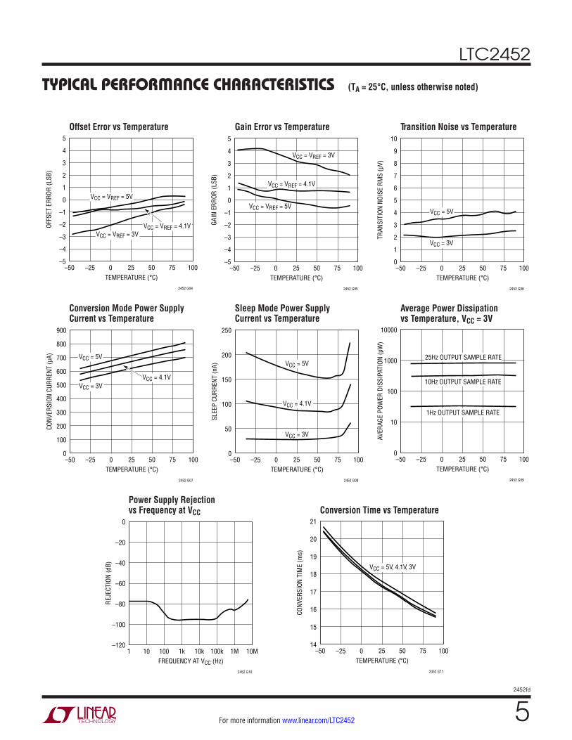
Typical perForMance characTerisTics
Note 1: Stresses beyond those listed under Absolute Maximum Ratings may cause permanent damage to the device. Exposure to any Absolute Maximum Rating condition for extended periods may affect device reliability and lifetime.Note 2. All voltage values are with respect to GND. VCC = 2.7V to 5.5V unless otherwise specified. VREFCM = VREF/2, FS = VREF
VIN = VIN+ – VIN
–, –VREF ≤ VIN ≤ VREF; VINCM = (VIN+ + VIN
–)/2.Note 3. Guaranteed by design, not subject to test.Note 4. Integral nonlinearity is defined as the deviation of a code from a straight line passing through the actual endpoints of the transfer curve. Guaranteed by design and test correlation.
Note 5: CS = VCC. A positive current is flowing into the DUT pin.Note 6: SCK = VCC or GND. SDO is high impedance.Note 7: See Figure 4.Note 8: See Figure 5.Note 9: Input sampling current is the average input current drawn from the input sampling network while the LTC2452 is actively sampling the input.Note 10: A positive current is flowing into the DUT pin.
TiMing characTerisTics
Integral Nonlinearity, VCC = 5V Integral Nonlinearity, VCC = 3V Maximum INL vs Temperature
(TA = 25°C, unless otherwise noted)
DIFFERENTIAL INPUT VOLTAGE (V)–5
INL
(LSB
)
1
3
2452 G01
–1
0
2
–2
–3–1–2–3–4 1 2 3 40 5
TA = –45°C, 25°C
TA = 90°C
DIFFERENTIAL INPUT VOLTAGE (V)–3
INL
(LSB
)
1
3
2452 G02
–1
0
2
–2
–3–1–2 1 20 3
TA = –45°C, 25°C, 90°C
TEMPERATURE (°C)–50
INL
(LSB
)
1
3
2452 G03
–1
0
2
–2
–3–25 25 50 750 100
VCC = VREF = 5V, 4.1V, 3V
LTC2452
52452fd
For more information www.linear.com/LTC2452
Typical perForMance characTerisTics
Offset Error vs Temperature Gain Error vs Temperature Transition Noise vs Temperature
Conversion Mode Power Supply Current vs Temperature
Sleep Mode Power Supply Current vs Temperature
Average Power Dissipationvs Temperature, VCC = 3V
Power Supply Rejection vs Frequency at VCC Conversion Time vs Temperature
(TA = 25°C, unless otherwise noted)
TEMPERATURE (°C)–50
OFFS
ET E
RROR
(LSB
)
1
5
2452 G04
–1
0
2
3
4
–2
–3
–4
–5–25 25 50 750 100
VCC = VREF = 5V
VCC = VREF = 4.1VVCC = VREF = 3V
TEMPERATURE (°C)–50
GAIN
ERR
OR (L
SB)
1
5
2452 G05
–1
0
2
3
4
–2
–3
–4
–5–25 25 50 750 100
VCC = VREF = 5V
VCC = VREF = 4.1V
VCC = VREF = 3V
TEMPERATURE (°C)–50
TRAN
SITI
ON N
OISE
RM
S (µ
V)
6
10
2452 G06
4
5
7
8
9
3
2
1
0–25 25 50 750 100
VCC = 5V
VCC = 3V
TEMPERATURE (°C)–50
CONV
ERSI
ON C
URRE
NT (µ
A)
900
2452 G07
400
500
600
700
800
300
200
100
0–25 25 50 750 100
VCC = 5V
VCC = 3VVCC = 4.1V
TEMPERATURE (°C)–50
SLEE
P CU
RREN
T (n
A)
250
2452 G08
150
200
100
50
0–25 25 50 750 100
VCC = 5V
VCC = 3V
VCC = 4.1V
TEMPERATURE (°C)–50
AVER
AGE
POW
ER D
ISSI
PATI
ON (µ
W)
10000
2452 G09
1000
100
10
0–25 25 50 750 100
25Hz OUTPUT SAMPLE RATE
10Hz OUTPUT SAMPLE RATE
1Hz OUTPUT SAMPLE RATE
FREQUENCY AT VCC (Hz)1
REJE
CTIO
N (d
B)
0
2452 G10
–20
–40
–60
–80
–100
–12010 1k 10k 100k 1M100 10M
TEMPERATURE (°C)–50
CONV
ERSI
ON T
IME
(ms)
21
2452 G11
20
16
17
18
19
15
14–25 25 50 750 100
VCC = 5V, 4.1V, 3V

LTC2452
62452fd
For more information www.linear.com/LTC2452
applicaTions inForMaTion
block DiagraM
pin FuncTionsSCK (Pin 1): Serial Clock Input. SCK synchronizes the serial data output. While digital data is available (the ADC is not in CONVERT state) and CS is LOW (ADC is not in SLEEP state) a new data bit is produced at the SDO output pin following every falling edge applied to the SCK pin.
GND (Pin 2): Ground. Connect to a ground plane through a low impedance connection.
REF (Pin 3): Reference Input. The voltage on REF can have any value between 2.5V and VCC. The reference voltage sets the full-scale range.
VCC (Pin 4): Positive Supply Voltage. Bypass to GND (Pin 2) with a 10µF capacitor in parallel with a low-series-inductance 0.1µF capacitor located as close to the LTC2452 as possible.
IN– (Pin 5), IN+ (Pin 6): Differential Analog Input.
CS (Pin 7): Chip Select (Active LOW) Digital Input. A LOW on this pin enables the SDO digital output. A HIGH on this pin places the SDO output pin in a high impedance state.
SDO (Pin 8): Three-State Serial Data Output. SDO is used for serial data output during the DATA OUTPUT state and can be used to monitor the conversion status.
Exposed Pad (Pin 9): Ground. Must be soldered to PCB ground. For prototyping purposes, this pad may remain floating.
Figure 1. Functional Block Diagram
16-BIT ΔΣA/D CONVERTER
DECIMATINGSINC FILTER
SCK
REF VCC
GND
IN+
IN–
SDO
CS
2452 BD
–
16-BIT ΔΣA/D CONVERTER
SPIINTERFACE
INTERNALOSCILLATOR
3 4
7
8
1
2, 9
6
5
CONVERTER OPERATION
Converter Operation Cycle
The LTC2452 is a low power, fully differential, delta-sigma analog-to-digital converter with a simple 3-wire SPI in-terface (see Figure 1). Its operation is composed of three successive states: CONVERT, SLEEP and DATA OUTPUT.
The operating cycle begins with the CONVERT state, is followed by the SLEEP state, and ends with the DATA OUT-PUT state (see Figure 2). The 3-wire interface consists of serial data output (SDO), serial clock input (SCK), and the active low chip select input (CS).
The CONVERT state duration is determined by the LTC2452 conversion time (nominally 16.6 milliseconds). Once

LTC2452
72452fd
For more information www.linear.com/LTC2452
applicaTions inForMaTion
Figure 2. LTC2452 State Transition Diagram
of data appears at the SDO pin following each falling edge detected at the SCK input pin and appears from MSB to LSB. The user can reliably latch this data on every rising edge of the external serial clock signal driving the SCK pin (see Figure 3).
The DATA OUTPUT state concludes in one of two different ways. First, the DATA OUTPUT state operation is completed once all 16 data bits have been shifted out and the clock then goes low. This corresponds to the 16th falling edge of SCK. Second, the DATA OUTPUT state can be aborted at any time by a LOW-to-HIGH transition on the CS input. Following either one of these two actions, the LTC2452 will enter the CONVERT state and initiate a new conversion cycle.
Power-Up Sequence
When the power supply voltage (VCC) applied to the con-verter is below approximately 2.1V, the ADC performs a power-on reset. This feature guarantees the integrity of the conversion result.
When VCC rises above this critical threshold, the converter generates an internal power-on reset (POR) signal for approximately 0.5ms. The POR signal clears all internal registers. Following the POR signal, the LTC2452 starts a conversion cycle and follows the succession of states shown in Figure 2. The first conversion result following POR is accurate within the specifications of the device if the power supply voltage VCC is restored within the operating range (2.7V to 5.5V) before the end of the POR time interval.
Ease of Use
The LTC2452 data output has no latency, filter settling delay or redundant results associated with the conversion cycle. There is a one-to-one correspondence between the conversion and the output data. Therefore, multiplexing multiple analog input voltages requires no special actions.
The LTC2452 performs offset calibrations every conver-sion. This calibration is transparent to the user and has no effect upon the cyclic operation described previously. The advantage of continuous calibration is stability of the ADC performance with respect to time and temperature.
The LTC2452 includes a proprietary input sampling scheme that reduces the average input current by several orders
DATA OUTPUT
SLEEP
CONVERT
POWER-ON RESET
YES
2452 F02
16TH FALLINGEDGE OF SCK
ORCS = HIGH?
SCK = LOWAND
CS = LOW?
NO YES
NO
started, this operation can not be aborted except by a low power supply condition (VCC < 2.1V) which generates an internal power-on reset signal.
After the completion of a conversion, the LTC2452 enters the SLEEP state and remains there until both the chip select and serial clock inputs are low (CS = SCK = LOW). Following this condition, the ADC transitions into the DATA OUTPUT state.
While in the SLEEP state, whenever the chip select input is pulled high (CS = HIGH), the LTC2452’s power supply current is reduced to less than 200nA. When the chip select input is pulled low (CS = LOW), and SCK is maintained at a HIGH logic level, the LTC2452 will return to a normal power consumption level. During the SLEEP state, the result of the last conversion is held indefinitely in a static register.
Upon entering the DATA OUTPUT state, SDO outputs the sign (D15) of the conversion result. During this state, the ADC shifts the conversion result serially through the SDO output pin under the control of the SCK input pin. There is no latency in generating this data and the result corresponds to the last completed conversion. A new bit

LTC2452
82452fd
For more information www.linear.com/LTC2452
applicaTions inForMaTionof magnitude when compared to traditional delta-sigma architectures. This allows external filter networks to in-terface directly to the LTC2452. Since the average input sampling current is 50nA, an external RC lowpass filter using 1kΩ and 0.1µF results in <1LSB additional error. Additionally, there is negligible leakage current between IN+ and IN–.
Reference Voltage Range
The LTC2453 reference input range is 2.5V to VCC. For the simplest operation, REF can be shorted to VCC.
Input Voltage Range
As mentioned in the Output Data Format section, the out-put code is given as 32768 • VIN/VREF + 32768. For VIN ≥ VREF, the output code is clamped at 65535 (all ones). For VIN ≤ –VREF, the output code is clamped at 0 (all zeroes).
The LTC2452 includes a proprietary system that can, typically, digitize each input 8LSB above VREF and below GND, if the differential input is within ±VREF. As an ex-ample (Figure 3), if the user desires to measure a signal slightly below ground, the user could set VIN
– = GND, and VREF = 5V. If VIN
+ = GND, the output code would be approximately 32768. If VIN
+ = GND – 8LSB = –1.22 mV, the output code would be approximately 32760.
The total amount of overrange and underrange capability is typically 31LSB for a given device. The 31LSB total is distributed between the overrange and underrange
Figure 3. Output Code vs VIN+ with VIN
– = 0
capability. For example, if the underrange capability is 8LSB, the overrange capability is typically 31 – 8 = 23LSB.
Output Data Format
The LTC2452 generates a 16-bit direct binary encoded result. It is provided as a 16-bit serial stream through the SDO output pin under the control of the SCK input pin (see Figure 4).
Letting VIN = (VIN+ – VIN
–), the output code is given as 32768 • VIN/VREF + 32768. The first bit output by the LTC2452, D15, is the MSB, which is 1 for VIN
+ ≥ VIN– and
0 for VIN+ < VIN
–. This bit is followed by successively less significant bits (D14, D13...) until the LSB is output by the LTC2452. Table 1 shows some example output codes.
During the data output operation the CS input pin must be pulled low (CS = LOW). The data output process starts
Table 1. LTC2452 Output Data FormatDIFFERENTIAL INPUT VOLTAGE VIN
+ – VIN–
D15 (MSB)
D14 D13 D12...D2 D1 D0 (LSB)
CORRESPONDING DECIMAL VALUE
≥VREF 1 1 1 1 1 1 65535
VREF – 1LSB 1 1 1 1 1 0 65534
0.5•VREF 1 1 0 0 0 0 49152
0.5•VREF – 1LSB 1 0 1 1 1 1 49151
0 1 0 0 0 0 0 32768
–1LSB 0 1 1 1 1 1 32767
–0.5•VREF 0 1 0 0 0 0 16384
–0.5•VREF – 1LSB 0 0 1 1 1 1 16383
≤ –VREF 0 0 0 0 0 0 0
VIN+/VREF
+–0.001
OUTP
UT C
ODE
4
12
20
0.001
2452 F03
–4
–12
0
8
16
–8
–16
–20–0.005 0 0.005 0.0015
SIGNALSBELOWGND

LTC2452
92452fd
For more information www.linear.com/LTC2452
applicaTions inForMaTion
Figure 4. Data Output Timing
D15
LSBSDO
SCK
D14 D13 D12 D11 D10 D9 D8 D7 D6 D5 D4 D3 D2 D0D1
2452 F04
t1t3
tKQ tlSCK thSCK
t2
CS
MSB
with the most significant bit of the result being present at the SDO output pin (SDO = D15) once CS goes low. A new data bit appears at the SDO output pin after each falling edge detected at the SCK input pin. The output data can be reliably latched by the user using the rising edge of SCK.
Conversion Status Monitor
For certain applications, the user may wish to monitor the LTC2452 conversion status. This can be achieved by holding SCK HIGH during the conversion cycle. In this condition, whenever the CS input pin is pulled low (CS = LOW), the SDO output pin will provide an indication of the conversion status. SDO = HIGH is an indication of a conversion cycle in progress while SDO = LOW is an indication of a completed conversion cycle. An example of such a sequence is shown in Figure 5.
Conversion status monitoring, while possible, is not re-quired for LTC2452 as its conversion time is fixed and equal
at approximately 16.6ms (23ms maximum). Therefore, external timing can be used to determine the completion of a conversion cycle.
SERIAL INTERFACE
The LTC2452 transmits the conversion result and receives the start of conversion command through a synchronous 3-wire interface. This interface can be used during the CONVERT and SLEEP states to assess the conversion status and during the DATA OUTPUT state to read the conversion result, and to trigger a new conversion.
Serial Interface Operation Modes
The modes of operation can be summarized as follows:
1) The LTC2452 functions with SCK idle high (commonly known as CPOL = 1) or idle low (commonly known as CPOL = 0).
Figure 5. Conversion Status Monitoring Mode
SLEEP
t1 t2
SDO
SCK = HIGH CONVERT2452 F05
CS

LTC2452
102452fd
For more information www.linear.com/LTC2452
applicaTions inForMaTion2) After the 16th bit is read, the user can choose one of
two ways to begin a new conversion. First, one can pull CS high (CS = ↑). Second, one can use a high-low transition on SCK (SCK = ↓).
3) At any time during the Data Output state, pulling CS high (CS = ↑) causes the part to leave the I/O state, abort the output and begin a new conversion.
4) When SCK = HIGH, it is possible to monitor the conver-sion status by pulling CS low and watching for SDO to go low. This feature is available only in the idle-high (CPOL = 1) mode.
Serial Clock Idle-High (CPOL = 1) Examples
In Figure 6, following a conversion cycle the LTC2452 automatically enters the low power sleep mode. The user can monitor the conversion status at convenient intervals using CS and SDO.
Pulling CS LOW while SCK is HIGH tests whether or not the chip is in the CONVERT state. While in the CONVERT state, SDO is HIGH while CS is LOW. In the SLEEP state, SDO is LOW while CS is LOW. These tests are not required operational steps but may be useful for some applications.
When the data is available, the user applies 16 clock cycles to transfer the result. The CS rising edge is then used to initiate a new conversion.
The operation example of Figure 7 is identical to that of Figure 6, except the new conversion cycle is triggered by the falling edge of the serial clock (SCK). A 17th clock pulse is used to trigger a new conversion cycle.
Serial Clock Idle-Low (CPOL = 0) Examples
In Figure 8, following a conversion cycle the LTC2452 automatically enters the low-power sleep state. The user determines data availability (and the end of conversion)
Figure 6. Idle-High (CPOL = 1) Serial Clock Operation Example. The Rising Edge of CS Starts a New Conversion
Figure 7. Idle-High (CPOL = 1) Clock Operation Example. A 17th Clock Pulse is Used to Trigger a New Conversion Cycle
D15
clk1 clk2 clk3 clk4 clk15 clk16
D14 D13 D12 D2 D1 D0SD0
SCK
CONVERT CONVERTSLEEP DATA OUTPUT
2452 F06
CS
D15 D14 D13 D12 D2 D1 D0SD0
clk1 clk2 clk3 clk4 clk15 clk16 clk17
SCK
CONVERT CONVERTSLEEP DATA OUTPUT
2452 F07
CS

LTC2452
112452fd
For more information www.linear.com/LTC2452
applicaTions inForMaTion
based upon external timing. The user then pulls CS low (CS = ↓) and uses 16 clock cycles to transfer the result. Following the 16th rising edge of the clock, CS is pulled high (CS = ↑), which triggers a new conversion.
The timing diagram in Figure 9 is identical to that of Figure 8, except in this case a new conversion is triggered by SCK. The 16th SCK falling edge triggers a new conversion cycle and the CS signal is subsequently pulled high.
Examples of Aborting Cycle Using CS
For some applications, the user may wish to abort the I/O cycle and begin a new conversion. If the LTC2452 is in the data output state, a CS rising edge clears the remain-
ing data bits from the output registers, aborts the output cycle and triggers a new conversion. Figure 10 shows an example of aborting an I/O with idle-high (CPOL = 1) and Figure 11 shows an example of aborting an I/O with idle-low (CPOL = 0).
A new conversion cycle can be triggered using the CS signal without having to generate any serial clock pulses as shown in Figure 12. If SCK is maintained at a low logic level, after the end of a conversion cycle, a new conver-sion operation can be triggered by pulling CS low and then high. When CS is pulled low (CS = LOW), SDO will output the sign (D15) of the result of the just completed conversion. While a low logic level is maintained at SCK
Figure 9. Idle-Low (CPOL = 0) Clock. The 16th SCK Falling Edge Triggers a New Conversion
Figure 8. Idle-Low (CPOL = 0) Clock. CS Triggers a New Conversion
D15 D14 D13 D12 D2 D1 D0
clk1 clk2 clk3 clk4 clk14 clk15 clk16
SCK
SD0
CONVERT CONVERTSLEEP DATA OUTPUT
2452 F08
CS
D15 D14 D13 D12 D2 D1 D0SD0
clk1 clk2 clk3 clk4 clk15clk14 clk16
SCK
CONVERT CONVERTSLEEP DATA OUTPUT
2452 F09
CS

LTC2452
122452fd
For more information www.linear.com/LTC2452
applicaTions inForMaTion
Figure 11. Idle-Low (CPOL = 0) Clock and Aborted I/O Example
Figure 12. Idle-Low (CPOL = 0) Clock and Minimum Data Output Length Example
Figure 10. Idle-High (CPOL = 1) Clock and Aborted I/O Example
D15 D14 D13
clk1 clk2 clk4clk3
CONVERT CONVERTSLEEP DATA OUTPUT
2452 F10
SD0
SCK
CS
D15 D14 D13SD0
clk1 clk2 clk3
SCK
CONVERT CONVERTSLEEP DATA OUTPUT
2452 F11
CS
SCK = LOW
SD0
CONVERT CONVERTSLEEP DATA OUTPUT
2452 F12
D15
CS

LTC2452
132452fd
For more information www.linear.com/LTC2452
pin and CS is subsequently pulled high (CS = HIGH) the remaining 15 bits of the result (D14:D0) are discarded and a new conversion cycle starts.
Following the aborted I/O, additional clock pulses in the CONVERT state are acceptable, but excessive signal tran-sitions on SCK can potentially create noise on the ADC during the conversion, and thus may negatively influence the conversion accuracy.
2-Wire Operation
The 2-wire operation modes, while reducing the number of required control signals, should be used only if the LTC2452 low power sleep capability is not required. In addition the option to abort serial data transfers is no longer available. Hardwire CS to GND for 2-wire operation.
Figure 13 shows a 2-wire operation sequence which uses an idle-high (CPOL = 1) serial clock signal. The conversion
Figure 13. 2-Wire, Idle-High (CPOL = 1) Serial Clock, Operation Example
status can be monitored at the SDO output. Following a conversion cycle, the ADC enters SLEEP state and the SDO output transitions from HIGH to LOW. Subsequently 16 clock pulses are applied to the SCK input in order to serially shift the 16 bit result. Finally, the 17th clock pulse is applied to the SCK input in order to trigger a new conversion cycle.
Figure 14 shows a 2-wire operation sequence which uses an idle-low (CPOL = 0) serial clock signal. The conversion status cannot be monitored at the SDO output. Following a conversion cycle, the LTC2452 bypasses the SLEEP state and immediately enters the DATA OUTPUT state. At this moment the SDO pin outputs the sign (D15) of the conversion result. The user must use external timing in order to determine the end of conversion and result avail-ability. Subsequently 16 clock pulses are applied to SCK in order to serially shift the 16-bit result. The 16th clock falling edge triggers a new conversion cycle.
applicaTions inForMaTion
Figure 14. 2-Wire, Idle-Low (CPOL = 0) Serial Clock Operation Example
2452 F13
D15 D14 D13 D12 D2 D1 D0SD0
clk1 clk2 clk3 clk4 clk15 clk16 clk17
SCK
CONVERT CONVERTSLEEP DATA OUTPUT
CS = LOW
2452 F14
D15 D14 D13 D12 D2 D1 D0SD0
CS = LOW
clk1 clk2 clk3 clk14clk4 clk15 clk16
SCK
CONVERT CONVERTDATA OUTPUT

LTC2452
142452fd
For more information www.linear.com/LTC2452
applicaTions inForMaTionPRESERVING THE CONVERTER ACCURACY
The LTC2452 is designed to minimize the conversion result’s sensitivity to device decoupling, PCB layout, anti-aliasing circuits, line and frequency perturbations. Nevertheless, in order to preserve the high accuracy capa-bility of this part, some simple precautions are desirable.
Digital Signal Levels
Due to the nature of CMOS logic, it is advisable to keep input digital signals near GND or VCC. Voltages in the range of 0.5V to VCC – 0.5V may result in additional current leakage from the part. Undershoot and overshoot should also be minimized, particularly while the chip is converting. It is thus beneficial to keep edge rates of about 10ns and limit overshoot and undershoot to less than 0.3V.
Noisy external circuitry can potentially impact the output under 2-wire operation. In particular, it is possible to get the LTC2452 into an unknown state if an SCK pulse is missed or noise triggers an extra SCK pulse. In this situ-ation, it is impossible to distinguish SDO = 1 (indicating conversion in progress) from valid “1” data bits. As such, CPOL = 1 is recommended for the 2-wire mode. The user should look for SDO = 0 before reading data, and look for SDO = 1 after reading data. If SDO does not return a “0” within the maximum conversion time (or return a “1” after a full data read), generate 16 SCK pulses to force a new conversion.
Driving VCC and GND
In relation to the VCC and GND pins, the LTC2452 com-bines internal high frequency decoupling with damping elements, which reduce the ADC performance sensitivity to PCB layout and external components. Nevertheless, the very high accuracy of this converter is best preserved by careful low and high frequency power supply decoupling.
A 0.1µF, high quality, ceramic capacitor in parallel with a 10µF ceramic capacitor should be connected between the VCC and GND pins, as close as possible to the pack-age. The 0.1µF capacitor should be placed closest to the ADC package. It is also desirable to avoid any via in the circuit path, starting from the converter VCC pin, passing through these two decoupling capacitors, and return-ing to the converter GND pin. The area encompassed
by this circuit path, as well as the path length, should be minimized.
Furthermore, as shown in Figure 15, GND is used as the negative reference voltage. It is thus important to keep the GND line quiet and connect GND through a low-impedance trace.
Very low impedance ground and power planes, and star connections at both VCC and GND pins, are preferable. The VCC pin should have two distinct connections: the first to the decoupling capacitors described above, and the second to the ground return for the power supply voltage source.
Driving REF
A simplified equivalent circuit for REF is shown in Figure 15. Like all other A/D converters, the LTC2452 is only as accurate as the reference it is using. Therefore, it is important to keep the reference line quiet by careful low and high frequency decoupling.
The LT6660 reference is an ideal match for driving the LTC2452’s REF pin. The LTC6660 is available in a 2mm × 2mm DFN package with 2.5V, 3V, 3.3V and 5V options.
Figure 15. LTC2452 Analog Input/Reference Equivalent Circuit
RSW15k
(TYP)ILEAK
ILEAK
VCC
VCC
VCC
VCC
CEQ0.35pF(TYP)
IN+
IN–
GND
REF
2452 F15
RSW15k
(TYP)ILEAK
ILEAK
RSW15k
(TYP)
ILEAK
ILEAK
RSW15k
(TYP)
ILEAK
ILEAK

LTC2452
152452fd
For more information www.linear.com/LTC2452
applicaTions inForMaTionA 0.1µF, high quality, ceramic capacitor in parallel with a 10µF ceramic capacitor should be connected between the REF and GND pins, as close as possible to the package. The 0.1µF capacitor should be placed closest to the ADC.
Driving VIN+ and VIN
–
The input drive requirements can best be analyzed using the equivalent circuit of Figure 16. The input signal VSIG is connected to the ADC input pins (IN+ and IN–) through an equivalent source resistance RS. This resistor includes both the actual generator source resistance and any additional optional resistors connected to the input pins. Optional input capacitors CIN are also connected to the ADC input pins. This capacitor is placed in parallel with the ADC input parasitic capacitance CPAR. Depending on the PCB layout, CPAR has typical values between 2pF and 15pF. In addition, the equivalent circuit of Figure 16 includes the converter equivalent internal resistor RSW and sampling capacitor CEQ.
There are some immediate trade-offs in RS and CIN without needing a full circuit analysis. Increasing RS and CIN can give the following benefits:
1) Due to the LTC2452’s input sampling algorithm, the input current drawn by either VIN
+ or VIN– over a conversion
cycle is typically 50nA. A high RS • CIN attenuates the high frequency components of the input current, and RS values up to 1k result in <1LSB error.
Figure 16. LTC2452 Input Drive Equivalent Circuit
2) The bandwidth from VSIG is reduced at the input pins (IN+, IN–). This bandwidth reduction isolates the ADC from high frequency signals, and as such provides simple anti-aliasing and input noise reduction.
3) Switching transients generated by the ADC are attenu-ated before they go back to the signal source.
4) A large CIN gives a better AC ground at the input pins, helping reduce reflections back to the signal source.
5) Increasing RS protects the ADC by limiting the current during an outside-the-rails fault condition.
There is a limit to how large RS • CIN should be for a given application. Increasing RS beyond a given point increases the voltage drop across RS due to the input current, to the point that significant measurement errors exist. Additionally, for some applications, increasing the RS • CIN product too much may unacceptably attenuate the signal at frequencies of interest.
For most applications, it is desirable to implement CIN as a high-quality 0.1µF ceramic capacitor and RS ≤ 1k. This capacitor should be located as close as possible to the actual VIN package pin. Furthermore, the area encompassed by this circuit path, as well as the path length, should be minimized.
ILEAK
ILEAK
RSW15k
(TYP)
ICONVCIN
IN+
VCC
SIG+
SIG–
RS
CEQ0.35pF(TYP)
CPAR
+–
2452 F16
ILEAK
ILEAK
RSW15k
(TYP)
ICONVCIN
IN–
VCC
RS
CEQ0.35pF(TYP)
CPAR
+–

LTC2452
162452fd
For more information www.linear.com/LTC2452
applicaTions inForMaTionIn the case of a 2-wire sensor that is not remotely grounded, it is desirable to split RS and place series resistors in the ADC input line as well as in the sensor ground return line, which should be tied to the ADC GND pin using a star connection topology.
Figure 17 shows the measured LTC2452 INL vs Input Voltage as a function of RS value with an input capacitor CIN = 0.1µF.
In some cases, RS can be increased above these guidelines. The input current is zero when the ADC is either in sleep or I/O modes. Thus, if the time constant of the input RC circuit t = RS • CIN, is of the same order of magnitude or longer than the time periods between actual conversions, then one can consider the input current to be reduced correspondingly.
These considerations need to be balanced out by the input signal bandwidth. The 3dB bandwidth ≈ 1/(2pRSCIN).
Finally, if the recommended choice for CIN is unacceptable for the user’s specific application, an alternate strategy is to eliminate CIN and minimize CPAR and RS. In practical terms, this configuration corresponds to a low impedance sensor directly connected to the ADC through minimum length traces. Actual applications include current measurements through low value sense resistors, temperature measure-ments, low impedance voltage source monitoring, and so on. The resultant INL vs VIN is shown in Figure 18. The measurements of Figure 18 include a capacitor CPAR cor-responding to a minimum sized layout pad and a minimum width input trace of about 1 inch length.
Figure 17. Measured INL vs Input Voltage, CIN = 0.1µF, VCC = 5V, TA = 25°C
Figure 18. Measured INL vs Input Voltage, CIN = 0, VCC = 5V, TA = 25°C
DIFFERENTIAL INPUT VOLTAGE (V)–5
INL
(LSB
) 2
6
10
3
2452 F17
–2
–6
0
4
8
–4
–8
–10–3–4 –1–2 1 2 40 5
RS = 10k
RS = 2k
RS = 1k RS = 0
CIN = 0.1µFVCC = 5VTA = 25°C
DIFFERENTIAL INPUT VOLTAGE (V)–5
INL
(LSB
) 2
6
10
3
2452 F18
–2
–6
0
4
8
–4
–8
–10–3–4 –1–2 1 2 40 5
RS = 10k
RS = 1k, 2k
RS = 0
CIN = 0VCC = 5VTA = 25°C

LTC2452
172452fd
For more information www.linear.com/LTC2452
applicaTions inForMaTionSignal Bandwidth, Transition Noise and Noise Equivalent Input Bandwidth
The LTC2452 includes a SINC1 type digital filter with the first notch located at f0 = 60Hz. As such, the 3dB input signal bandwidth is 26.54Hz. The calculated LTC2452 input signal attenuation vs frequency over a wide frequency range is shown in Figure 19. The calculated LTC2452 input signal attenuation vs frequency at low frequencies is shown in Figure 20. The converter noise level is about 2.2µVRMS and can be modeled by a white noise source connected at the input of a noise-free converter.
On a related note, the LTC2452 uses two separate A/D converters to digitize the positive and negative inputs. Each of these A/D converters has 2.2µVRMS transition noise. If one of the input voltages is within this small transition
noise band, then the output will fluctuate one bit, regard-less of the value of the other input voltage. If both of the input voltages are within their transition noise bands, the output can fluctuate 2 bits.
For a simple system noise analysis, the VIN drive circuit can be modeled as a single-pole equivalent circuit character-ized by a pole location fi and a noise spectral density ni. If the converter has an unlimited bandwidth, or at least a bandwidth substantially larger than fi, then the total noise contribution of the external drive circuit would be:
Vn = ni p / 2 • fi
Then, the total system noise level can be estimated as the square root of the sum of (Vn
2) and the square of the LTC2452 noise floor (~2.2µV2).
Figure 19. LTC2452 Input Signal Attenuation vs Frequency Figure 20. LTC2452 Input Signal Attenuation vs Frequency (Low Frequencies)
INPUT SIGNAL FREQUENCY (MHz)
0
INPU
T SI
GNAL
ATT
ENUA
TION
(dB)
–40
0
1.00 1.25 1.50
2452 F19
–60
–80
–20
–1002.5 5.0 7.5
INPUT SIGNAL FREQUENCY (Hz)0
INPU
T SI
GNAL
ATT
ENUA
TIOI
N (d
B)
–20
–10
0
480
2452 F20
–30
–40
–25
–15
–5
–35
–45
–5012060 240180 360 420 540300 600

LTC2452
182452fd
For more information www.linear.com/LTC2452
Typical applicaTion
0.1µFVCC
IN+
IN–
2452 TA02
0.1µF
92
43
0.1µF
0.1µF
0.1µF
1k
1k
42GNDGND1µF
1µF
1k
IN OUT
U2LT6660HCDC-5
V+
3 1
5
6
8
1
7
VCC
VCC
GND
REF+
10V5V
CSSCK/SCLMOSI/SDAMISO/SDO
GND GND GND
12
6475
1µFVCC V+
1383
TOCONTROLLER
CS SCK SDO
1 2 3
EXT+5VJP1
U1*
IN+REF+
REF–
VCC
GNDIN–
LTC2452CS
SCK
SDO

LTC2452
192452fd
For more information www.linear.com/LTC2452
package DescripTionPlease refer to http://www.linear.com/designtools/packaging/ for the most recent package drawings.
DDB Package8-Lead Plastic DFN (3mm × 2mm)
(Reference LTC DWG # 05-08-1702 Rev B)
2.00 ±0.10(2 SIDES)
NOTE:1. DRAWING CONFORMS TO VERSION (WECD-1) IN JEDEC PACKAGE OUTLINE M0-229 2. DRAWING NOT TO SCALE 3. ALL DIMENSIONS ARE IN MILLIMETERS4. DIMENSIONS OF EXPOSED PAD ON BOTTOM OF PACKAGE DO NOT INCLUDE MOLD FLASH. MOLD FLASH, IF PRESENT, SHALL NOT EXCEED 0.15mm ON ANY SIDE5. EXPOSED PAD SHALL BE SOLDER PLATED6. SHADED AREA IS ONLY A REFERENCE FOR PIN 1 LOCATION ON THE TOP AND BOTTOM OF PACKAGE
0.40 ± 0.10
BOTTOM VIEW—EXPOSED PAD
0.56 ± 0.05(2 SIDES)
0.75 ±0.05
R = 0.115TYPR = 0.05
TYP
2.15 ±0.05(2 SIDES)
3.00 ±0.10(2 SIDES)
14
85
PIN 1 BARTOP MARK
(SEE NOTE 6)
0.200 REF
0 – 0.05
(DDB8) DFN 0905 REV B
0.25 ± 0.050.50 BSC
PIN 1R = 0.20 OR0.25 × 45°CHAMFER
0.25 ± 0.05
2.20 ±0.05(2 SIDES)
RECOMMENDED SOLDER PAD PITCH AND DIMENSIONS
0.61 ±0.05(2 SIDES)
1.15 ±0.05
0.70 ±0.05
2.55 ±0.05
PACKAGEOUTLINE
0.50 BSC

LTC2452
202452fd
For more information www.linear.com/LTC2452
package DescripTionPlease refer to http://www.linear.com/designtools/packaging/ for the most recent package drawings.
TS8 Package8-Lead Plastic TSOT-23
(Reference LTC DWG # 05-08-1637 Rev A)
1.50 – 1.75(NOTE 4)
2.80 BSC
0.22 – 0.36 8 PLCS (NOTE 3)
DATUM ‘A’
0.09 – 0.20(NOTE 3)
TS8 TSOT-23 0710 REV A
2.90 BSC(NOTE 4)
0.65 BSC
1.95 BSC
0.80 – 0.90
1.00 MAX0.01 – 0.10
0.20 BSC
0.30 – 0.50 REF
PIN ONE ID
NOTE:1. DIMENSIONS ARE IN MILLIMETERS2. DRAWING NOT TO SCALE3. DIMENSIONS ARE INCLUSIVE OF PLATING4. DIMENSIONS ARE EXCLUSIVE OF MOLD FLASH AND METAL BURR5. MOLD FLASH SHALL NOT EXCEED 0.254mm6. JEDEC PACKAGE REFERENCE IS MO-193
3.85 MAX
0.40MAX
0.65REF
RECOMMENDED SOLDER PAD LAYOUTPER IPC CALCULATOR
1.4 MIN2.62 REF
1.22 REF

LTC2452
212452fd
For more information www.linear.com/LTC2452
Information furnished by Linear Technology Corporation is believed to be accurate and reliable. However, no responsibility is assumed for its use. Linear Technology Corporation makes no representa-tion that the interconnection of its circuits as described herein will not infringe on existing patent rights.
revision hisToryREV DATE DESCRIPTION PAGE NUMBER
C 03/10 Updated Analog Inputs and References sectionAdded text to Input Voltage Range section
38
D 03/14 Changed VIN+ and VIN
– Input Voltage Range (MAX) to VREF 3
(Revision history begins at Rev C)

LTC2452
222452fd
For more information www.linear.com/LTC2452 LINEAR TECHNOLOGY CORPORATION 2013
LT 0314 REV D • PRINTED IN USALinear Technology Corporation1630 McCarthy Blvd., Milpitas, CA 95035-7417(408) 432-1900 ● FAX: (408) 434-0507 ● www.linear.com/LTC2452
relaTeD parTsPART NUMBER DESCRIPTION COMMENTS
LT1236A-5 Precision Bandgap Reference, 5V 0.05% Max, 5ppm/°C Drift
LT1461 Micropower Series Reference, 2.5V 0.04% Max, 3ppm/°C Drift
LT1790 Micropower Precision Reference in TSOT-23-6 Package 60µA Max Supply Current, 10ppm/°C Max Drift, 1.25V, 2.048V, 2.5V, 3V, 3.3V, 4.096V and 5V Options
LTC2440 24-Bit No Latency ∆Σ™ ADC 200nVRMS Noise, 4kHz Output Rate, 15ppm INL
LTC2480 16-Bit, Differential Input, No Latency ∆Σ ADC, with PGA, Temp. Sensor, SPI
Easy-Drive Input Current Cancellation, 600nVRMS Noise, Tiny 10-Lead DFN Package
LTC2481 16-Bit, Differential Input, No Latency ∆Σ ADC, with PGA, Temp. Sensor, I2C
Easy-Drive Input Current Cancellation, 600nVRMS Noise, Tiny 10-Lead DFN Package
LTC2482 16-Bit, Differential Input, No Latency ∆Σ ADC, SPI Easy-Drive Input Current Cancellation, 600nVRMS Noise, Tiny 10-Lead DFN Package
LTC2483 16-Bit, Differential Input, No Latency ∆Σ ADC, I2C Easy-Drive Input Current Cancellation, 600nVRMS Noise, Tiny 10-Lead DFN Package
LTC2484 24-Bit, Differential Input, No Latency ∆Σ ADC, SPI with Temp. Sensor
Easy-Drive Input Current Cancellation, 600nVRMS Noise, Tiny 10-Lead DFN Package
LTC2485 24-Bit, Differential Input, No Latency ∆Σ ADC, I2C with Temp. Sensor
Easy-Drive Input Current Cancellation, 600nVRMS Noise, Tiny 10-Lead DFN Package
LTC6241 Dual, 18MHz, Low Noise, Rail-to-Rail Op Amp 550nVP-P Noise, 125µV Offset Max
LT6660 Micropower References in 2mm × 2mm DFN Package, 2.5V, 3V, 3.3V, 5V
20ppm/°C Max Drift, 0.2% Max
LTC2450/LTC2450-1 Easy-to-Use, Ultra-Tiny 16-Bit ADC, SPI 2 LSB INL, 50nA Sleep Current, Tiny 2mm × 2mm DFN-6 Package, 30Hz/60Hz Output Rate
LTC2451/LTC2453 Easy-to-Use, Ultra-Tiny 16-Bit Single-Ended/Differential ADC, I2C
2 LSB INL, 50nA Sleep Current, Tiny 3mm × 2mm DFN-8 or TSOT Package, Programmable 30Hz/60Hz Output Rates
LTC2470/LTC2472 Selectable 233sps/833sps, 16-Bit ADC, SPI, Single-Ended/Differential
10ppm/°C Integrated Precision Reference, 3mm × 3mm DFN-12 or MSOP-12 Package
LTC2471/LTC2473 Selectable 233sps/833sps, 16-Bit Single-Ended/Differential ADC, I2C
10ppm/°C Integrated Precision Reference, 3mm × 3mm DFN-12 or MSOP-12 Package