ltc4121/ltc4121-4.2 - 40v 400ma synchronous step-down ......pin output voltage low i = 2ma 550 mv...
TRANSCRIPT

LTC4121/LTC4121-4.2
14121fc
For more information www.linear.com/LTC4121
TYPICAL APPLICATION
FEATURES DESCRIPTION
40V 400mA Synchronous Step-Down Battery Charger
The LTC®4121 is a 400mA constant-current/constant-voltage (CC/CV) synchronous step-down battery charger. In addition to CC/CV operation, the LTC4121 regulates its input voltage to a programmable percentage of the input open-circuit voltage. This technique maintains maximum power transfer with high impedance input sources such as solar panels.
An external resistor programs the charge current up to 400mA. The LTC4121-4.2 is suitable for charging Li-Ion/Polymer batteries, while the programmable float voltage of the LTC4121 is suitable for several battery chemistries.
The LTC4121 and LTC4121-4.2 include an accurate RUN pin threshold, low voltage battery preconditioning and bad battery fault detection, timer termination, auto-recharge, and NTC temperature qualified charging. The FAULT pin provides an indication of bad battery or temperature faults.
Once charging is terminated, the LTC4121 signals end-of-charge via the CHRG pin, and enters a low current SLEEP mode. An auto-restart feature starts a new charging cycle if the battery voltage drops by 2.2%.
LTC4121 Efficiency vs VIN at VFLOAT = 8.4V
APPLICATIONS
n Wide Input Voltage Range: 4.4V to 40V n Temperature Compensated Input Voltage
Regulation for Maximum Power Point Tracking (MPPT)
n Adjustable Float Voltage 3.5V to 18V (LTC4121) n Fixed 4.2V Float Voltage Option (LTC4121-4.2) n High Efficiency: Up to 95% n 50mA to 400mA Programmable Charge Current n ±1% Feedback Voltage Accuracy n Programmable 5% Accurate Charge Current n Thermally Enhanced, Low Profile (0.75mm)
16-Lead (3mm × 3mm) QFN Package
n Handheld Instruments n Solar Powered Devices n Industrial/Military Sensors and Devices
L, LT, LTC, LTM, Linear Technology, the Linear logo and Burst Mode are registered trademarks of Linear Technology Corporation. All other trademarks are the property of their respective owners.
INTVCC
BOOST
SW
CHGSNS
BAT
FB
FBG
IN
RUN
MPPT
PROG
LTC4121
GND
10k10µF
RPROG
VINVBAT + 200mVTO 40V
22nFSLF6025T-470MR48
2.2µF
FREQ +
22µF1.96M
787k
4121 TA01a
Li-Ion
+–
High Efficiency, Wide Input Voltage Range Charging with LTC4121
VIN (V)5
87
EFFI
CIEN
CY (%
)
89
91
93
95
97
10 15 20
4121 TA01b
25 30 35 40
200mA, RPROG = 6.04k400mA, RPROG = 3.01k
VBAT = 8.3V

LTC4121/LTC4121-4.2
24121fc
For more information www.linear.com/LTC4121
ABSOLUTE MAXIMUM RATINGS
IN, RUN, CHRG, FAULT, MPPT ................... –0.3V to 43VBOOST ................................... VSW – 0.3V to (VSW + 6V)SW (DC) ........................................ –0.3V to (VIN + 0.3V)SW (Pulsed <100ns) ......................–1.5V to (VIN + 1.5V)CHGSNS, BAT, FB/BATSNS, FBG ................ –0.3V to 18VFREQ, NTC, PROG, INTVCC .......................... –0.3V to 6VICHGSNS, IBAT ..................................................... ±600mA
(Note 1)
ORDER INFORMATION
LEAD FREE FINISH TAPE AND REEL PART MARKING PACKAGE DESCRIPTION TEMPERATURE RANGE
LTC4121EUD#PBF LTC4121EUD#TRPBF LGHC 16-Lead (3mm × 3mm) Plastic QFN –40°C to 125°C
LTC4121IUD#PBF LTC4121IUD#TRPBF LGHC 16-Lead (3mm × 3mm) Plastic QFN –40°C to 125°C
LTC4121EUD-4.2#PBF LTC4121EUD-4.2#TRPBF LGMV 16-Lead (3mm × 3mm) Plastic QFN –40°C to 125°C
LTC4121IUD-4.2#PBF LTC4121IUD-4.2#TRPBF LGMV 16-Lead (3mm × 3mm) Plastic QFN –40°C to 125°C
Consult LTC Marketing for parts specified with wider operating temperature ranges.For more information on lead free part marking, go to: http://www.linear.com/leadfree/ For more information on tape and reel specifications, go to: http://www.linear.com/tapeandreel/. Some packages are available in 500 unit reels through designated sales channels with #TRMPBF suffix.
LTC4121 LTC4121-4.2
16 15 14 13
5 6 7 8
TOP VIEW
GND
UD PACKAGE16-LEAD (3mm × 3mm) PLASTIC QFN
9
10
11
12
4
3
2
1INTVCC
BOOST
IN
SW
NTC
FBG
FB
BAT
RUN
FAULT
CHRG
PROG
GND
MPP
T
FREQ
CHGS
NS
TJMAX = 125°C, θJA = 54°C/W
EXPOSED PAD (PIN 17) IS GND, MUST BE SOLDERED TO PCB TO OBTAIN θJA
16 15 14 13
5 6 7 8
TOP VIEW
GND
UD PACKAGE16-LEAD (3mm × 3mm) PLASTIC QFN
9
10
11
12
4
3
2
1INTVCC
BOOST
IN
SW
NTC
NC
BATSNS
BAT
RUN
FAULT
CHRG
PROG
GND
MPP
T
FREQ
CHGS
NS
TJMAX = 125°C, θJA = 54°C/W
EXPOSED PAD (PIN 17) IS GND, MUST BE SOLDERED TO PCB TO OBTAIN θJA
PIN CONFIGURATION
ICHRG, IFAULT, ........................................................±5mAIFB, IFBG (LTC4121) .................................................±5mAIBATSNS (LTC4121-4.2) ...........................................±5mAIINTVCC .................................................................. –5mAOperating Junction Temperature Range (Note 2) .................................................. –40°C to 125°CStorage Temperature Range .................... –65°C to 150°
LTC4121 OptionsPART NUMBER FLOAT VOLTAGE
LTC4121 Programmable
LTC4121-4.2 4.2V Fixed
(http://www.linear.com/product/LTC4121#orderinfo)

LTC4121/LTC4121-4.2
34121fc
For more information www.linear.com/LTC4121
ELECTRICAL CHARACTERISTICS The l denotes the specifications which apply over the specified operating junction temperature range, otherwise specifications are at TA = 25°C. VIN = VRUN = 15V, VCHGSNS = VBAT = 4V, RPROG = 3.01k, VFB = 2.29V (LTC4121), VBATSNS = 4V (LTC4121-4.2). Current into a pin is positive out of a pin is negative. (Note 2)
SYMBOL PARAMETER CONDITIONS MIN TYP MAX UNITS
Operating Input Supply Range l 4.4 40 V
Battery Voltage Range LTC4121 (Note 3) 0 18 V
LTC4121-4.2 0 4.2 V
IIN DC Supply Current Switching: FREQ = GND 3.5 mA
Standby Mode: (Note 4) l 142 260 µA
Sleep Mode: (Note 4) LTC4121-4.2: VBATSNS = 4.4V LTC4121: VFB = 2.51V (Note 6)
l
60
110
µA
Disabled Mode: VSD < VRUN < VEN (Note 4) l 37 80 µA
Shutdown Mode: (Note 4) l 20 40 µA
∆VDUVLO Differential Undervoltage Lockout VIN – VBAT Falling, VIN = 5V (LTC4121) VIN – VBATSNS Falling, VIN = 5V (LTC4121-4.2)
l 20 80 160 mV
Hysteresis VIN – VBAT Rising, VIN = 5V (LTC4121) VIN – VBATSNS Rising, VIN = 5V (LTC4121-4.2)
115 mV
UVINTVCC INTVCC Undervoltage Lockout (Note 5) INTVCC Rising, VIN = INTVCC + 100mV l 4.00 4.15 4.26 V
Hysteresis INTVCC Falling 220 mV
Battery Charger
IBAT BAT Standby Current Standby Mode (LTC4121) (Notes 4, 8, 9) Standby Mode (LTC4121-4.2) (Notes 4, 8, 9)
l
l
2.5 50
4.5 1000
µA nA
BAT Shutdown Current Shutdown Mode (LTC4121) (Notes 4, 8, 9) Shutdown Mode (LTC4121-4.2) (Notes 4, 8, 9)
l
l
1100 10
2000 1000
nA nA
IBATSNS BATSNS Standby Current (LTC4121-4.2) Standby Mode (Notes 4, 8, 9) l 5.4 10 µA
BATSNS Shutdown Current (LTC4121-4.2) Shutdown Mode (Notes 4, 8, 9) l 1100 2000 nA
IFB Feedback Pin Bias Current (LTC4121) VFB = 2.5V (Note 6) l 25 60 nA
IFBG_LEAK Feedback Ground Leakage Current (LTC4121)
Shutdown Mode (Note 4) l 1 µA
RFBG Feedback Ground Return Resistance (LTC4121)
l 1000 2000 Ω
VFB(REG) Feedback Pin Regulation Voltage (LTC4121)
(Note 6) 2.393 2.400 2.407 V
l 2.370 2.418 V
VFLOAT Regulated Float Voltage (LTC4121-4.2) 4.188 4.200 4.212 V
l 4.148 4.231 V
ICHG Battery Charge Current RPROG = 3.01k l 383 402 421 mA
RPROG = 24.3k l 45 50 55 mA
VRCHG Battery Recharge Threshold VFB Falling Relative to VFB(REG) (LTC4121) l –38 –49 –62 mV
VRCHG_4.2 VBATSNS Falling Relative to VFLOAT (LTC4121-4.2) l –70 –93 –114 mV
hPROG Ratio of BAT Current to PROG Current VTRKL < VFB < VFB(REG) (LTC4121), VTRKL_42 < VBATSNS < VFLOAT (LTC4121-4.2)
988 mA/mA
VPROG PROG Pin Servo Voltage l 1.206 1.227 1.248 V
RSNS CHGSNS-BAT Sense Resistor IBAT = –100mA 300 mΩ

LTC4121/LTC4121-4.2
44121fc
For more information www.linear.com/LTC4121
ELECTRICAL CHARACTERISTICS The l denotes the specifications which apply over the specified operating junction temperature range, otherwise specifications are at TA = 25°C. VIN = VRUN = 15V, VCHGSNS = VBAT = 4V, RPROG = 3.01k, VFB = 2.29V (LTC4121), VBATSNS = 4V (LTC4121-4.2). Current into a pin is positive out of a pin is negative. (Note 2)
SYMBOL PARAMETER CONDITIONS MIN TYP MAX UNITS
ILOWBAT Low Battery Linear Charge Current VFB < VTRKL, VBAT = 2.6V (LTC4121) (Note 6) 6 9 16 mA
VBATSNS < VTRKL_4.2, VBAT = 2.6V (LTC4121-4.2)
VLOWBAT Low Battery Threshold Voltage VBAT Rising (LTC4121) VBATSNS Rising (LTC4121-4.2)
l 2.15 2.21 2. 28 V
Hysteresis 147 mV
ITRKL Switch Mode Trickle Charge Current VLOWBAT < VBAT, VFB < VTRKL (LTC4121) (Note 6) ICHG/10 mA
VLOWBAT < VBATSNS < VTRKL_42 (LTC4121-4.2)
PROG Pin Servo Voltage in Trickle Charge VLOWBAT < VBAT, VFB > VTRKL (LTC4121) (Note 6) 122 mV
VLOWBAT < VBATSNS < VTRKL_42 (LTC4121-4.2)
VTRKL Trickle Charge Threshold (LTC4121) VFB Rising (Note 6) l 1.65 1.68 1.71 V
Hysteresis (LTC4121) VFB Falling (Note 6) 50 mV
VTRKL_4.2 Trickle Charge Threshold (LTC4121-4.2) VBATSNS Rising l 2.86 2.91 2.98 V
Hysteresis (LTC4121-4.2) VBATSNS Falling 88 mV
hC/10 End of Charge Indication Current Ratio (Note 7) 0.1 mA/mA
Safety Timer Termination Period 1.3 2.0 2.8 hrs
Bad Battery Termination Timeout 19 30 42 min
Switcher
fOSC Switching Frequency FREQ = INTVCC l 1.0 1.5 2.0 MHz
FREQ = GND l 0.5 0.75 1.0 MHz
tMIN_ON Minimum Controllable On-Time 120 ns
Duty Cycle Maximum 94 %
Top Switch RDSON ISW = –100mA 0.8 Ω
Bottom Switch RDSON ISW = 100mA 0.5 Ω
IPEAK Peak Inductor Current Limit Measured Across RSNS with a 15µH Inductor in Series with RSNS (Note 10)
585 1050 1250 mA
ISW Switch Pin Current (Note 9) IN Open-Circuit, VBAT = VSW = 4.2V (LTC4121-4.2) l 7 15 µA
IN Open-Circuit, VBAT = VSW = 8.4V (LTC4121) l 15 30 µA
Status Pins FAULT, CHRG
Pin Output Voltage Low I = 2mA 550 mV
Pin Leakage Current V = 43V, Pin High-Impedance 0 1 µA
NTC
Cold Temperature VNTC/VINTVCC Fault Rising VNTC Threshold l 73 74 75 %INTVCC
Falling VNTC Threshold 72 %INTVCC
Hot Temperature VNTC/VINTVCC Fault Falling VNTC Threshold l 35.5 36.5 37.5 %INTVCC
Rising VNTC Threshold 37.5 %INTVCC
NTC Disable Voltage Falling VNTC Threshold l 1 2 3 %INTVCC
Rising VNTC Threshold 3 %INTVCC
NTC Input Leakage Current VNTC = VINTVCC –50 50 nA

LTC4121/LTC4121-4.2
54121fc
For more information www.linear.com/LTC4121
SYMBOL PARAMETER CONDITIONS MIN TYP MAX UNITS
RUN
VEN Enable Threshold VRUN Rising l 2.35 2.45 2.55 V
Hysteresis VRUN Falling 200 mV
Run Pin Input Current VRUN = 40V 0.01 0.1 µA
VSD Shutdown Threshold VRUN Falling l 0.4 1.2 V
Hysteresis 220 mV
FREQ
FREQ Pin Input Low l 0.4 V
FREQ Pin Input High l 3.6 V
FREQ Pin Input Current 0 < VFREQ < VINTVCC ±1 µA
MPPT
IMPPT MPPT Pin Leakage Current VMPPT = 4.2V l 15 1000 nA
TMP MPPT Sample Period Period Between Charger Disabled Events 28 s
PWMP MPPT Sample Pulse Width Charger Disabled Pulse Width 36 ms
KF Internal Divider Gain Internal DAC Voltage as a Ratio to VIN 0.098 0.1 0.102 V/V
VMP(OS) MPPT Error Amp Gain Offset VMPPT – VDAC, IBAT = 50%• ICHG 10 –45 –100 mV
ELECTRICAL CHARACTERISTICS The l denotes the specifications which apply over the specified operating junction temperature range, otherwise specifications are at TA = 25°C. VIN = VRUN = 15V, VCHGSNS = VBAT = 4V, RPROG = 3.01k, VFB = 2.29V (LTC4121), VBATSNS = 4V (LTC4121-4.2). Current into a pin is positive out of a pin is negative. (Note 2)
Note 1: Stresses beyond those listed under Absolute Maximum Ratings may cause permanent damage to the device. Exposure to any Absolute Maximum Rating condition for extended periods may affect device reliability and lifetime.Note 2: The LTC4121 is tested under pulsed load conditions such that TJ ≈ TA. The LTC4121E is guaranteed to meet performance specifications for junction temperatures from 0°C to 85°C. Specifications over the –40°C to 125°C operating junction temperature range are assured by design, characterization and correlation with statistical process controls. The LTC4121I is guaranteed over the full –40°C to 125°C operating junction temperature range. Note that the maximum ambient temperature consistent with these specifications is determined by specific operating conditions in conjunction with board layout, the rated package thermal impedance, and other environmental factors.Note 3: If a battery voltage greater than 11V can be hot plugged to the LTC4121 a reverse blocking diode is required in series with the BAT pin to prevent large inrush current into the low impedance BAT pin.
Note 4: Standby mode occurs when the LTC4121/LTC4121-4.2 stops switching due to an NTC fault, MPPT pause, or when the charge current has dropped low enough to enter Burst Mode operation. Disabled mode occurs when VRUN is between VSD and VEN. Shutdown mode occurs when VRUN is below VSD or when the differential undervoltage lockout is engaged. Sleep mode occurs after a timeout while the battery voltage remains above the VRCHG or VRCHG_42 threshold.Note 5: The internal supply INTVCC should only be used for the NTC divider, it should not be used for any other loadsNote 6: For the LTC4121, the FB pin is measured with a resistance of 588k in series with the pin.Note 7: hC/10 is expressed as a fraction of measured full charge current as measured at the PROG pin voltage when the CHRG pin de-asserts. Note 8: In an application circuit with an inductor connected from SW to CHGSNS, the total battery leakage current when disabled is the sum of IBATSNS and ISW (LTC4121-4.2) or IBAT and IFBG_LEAK and ISW (LTC4121).Note 9: When no supply is present at IN, the SW powers IN through the body diode of the top side switch. This may cause additional SW pin current depending on the load present at IN.Note 10: Guaranteed by design and/or correlation to static test.
LTC4121/LTC4121-4.2
64121fc
For more information www.linear.com/LTC4121
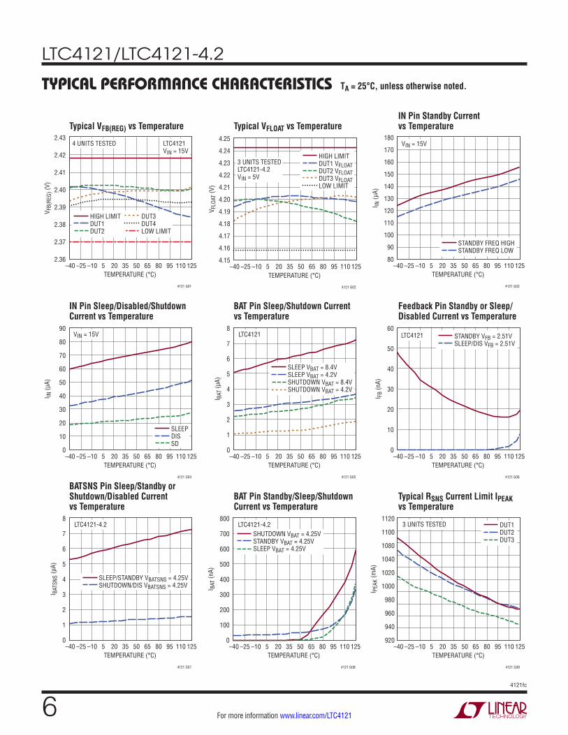
TYPICAL PERFORMANCE CHARACTERISTICS
IN Pin Sleep/Disabled/Shutdown Current vs Temperature
BAT Pin Sleep/Shutdown Current vs Temperature
Feedback Pin Standby or Sleep/Disabled Current vs Temperature
BATSNS Pin Sleep/Standby or Shutdown/Disabled Current vs Temperature
BAT Pin Standby/Sleep/Shutdown Current vs Temperature
Typical VFB(REG) vs Temperature Typical VFLOAT vs TemperatureIN Pin Standby Current vs Temperature
TEMPERATURE (°C)–40
4.15
V FLO
AT (V
)
4.16
4.17
4.23
4.22
4.21
4.20
4.18
4.19
4.25
4.24
–25 –10 5 20
4121 G02
35 50 65 80 95 110 125
3 UNITS TESTEDLTC4121-4.2VIN = 5V
HIGH LIMITDUT1 VFLOATDUT2 VFLOATDUT3 VFLOATLOW LIMIT
TEMPERATURE (°C)–40
0
I IN (µ
A)
60
50
40
30
10
20
90
80
70
–25 –10 5 20
4121 G04
35 50 65 80 95 110 125
SLEEPDISSD
VIN = 15V
TEMPERATURE (°C)–40
2.36
V FB(
REG)
(V)
2.37
2.38
2.41
2.40
2.39
2.43
2.42
–25 –10 5 20
4121 G01
35 50 65 80 95 110 125
4 UNITS TESTED
HIGH LIMITDUT1DUT2
DUT3DUT4LOW LIMIT
LTC4121VIN = 15V
TEMPERATURE (°C)–40
80
I IN (µ
A)
90
100
160
150
140
130
110
120
180
170
–25 –10 5 20
4121 G03
35 50 65 80 95 110 125
STANDBY FREQ HIGHSTANDBY FREQ LOW
VIN = 15V
TEMPERATURE (°C)–40
0
I BAT
(µA)
6
5
4
3
1
2
8
7
–25 –10 5 20
4121 G05
35 50 65 80 95 110 125
SLEEP VBAT = 8.4VSLEEP VBAT = 4.2VSHUTDOWN VBAT = 8.4VSHUTDOWN VBAT = 4.2V
LTC4121
TEMPERATURE (°C)–40
0
I FB
(nA)
50
40
30
10
20
60
–25 –10 5 20
4121 G06
35 50 65 80 95 110 125
STANDBY VFB = 2.51VSLEEP/DIS VFB = 2.51V
LTC4121
TEMPERATURE (°C)–40
0
I BAT
SNS
(µA)
6
5
4
3
1
2
8
7
–25 –10 5 20
4121 G07
35 50 65 80 95 110 125
SLEEP/STANDBY VBATSNS = 4.25VSHUTDOWN/DIS VBATSNS = 4.25V
LTC4121-4.2
TEMPERATURE (°C)–40
0
I BAT
(nA)
600
500
400
300
100
200
800
700
–25 –10 5 20
4121 G08
35 50 65 80 95 110 125
SHUTDOWN VBAT = 4.25VSTANDBY VBAT = 4.25VSLEEP VBAT = 4.25V
LTC4121-4.2
Typical RSNS Current Limit IPEAK vs Temperature
TEMPERATURE (°C)–40
920
I PEA
K (m
A)
1080
1040
1020
1000
940
960
980
1120
1100
–25 –10 5 20
4121 G09
35 50 65 80 95 110 125
DUT1DUT2DUT3
3 UNITS TESTED
TA = 25°C, unless otherwise noted.

LTC4121/LTC4121-4.2
74121fc
For more information www.linear.com/LTC4121
TYPICAL PERFORMANCE CHARACTERISTICS
Typical Burst Mode WaveformsIN Pin Shutdown Current vs Input Voltage
Burst Mode Trigger Current
Typical Battery Charge Current vs Temperature
Typical Solar Charging Cycle
Efficiency vs IBAT
IBAT (mA)0
40
EFFI
CIEN
CY (%
)
70
60
50
100
80
90
100
4121 G10
200 300 400
VIN = 9VVIN = 14VVIN = 19VVIN = 24V
LTC4121-42VBAT = 4.2VFREQ = LOWLSW = SLF12575T-470M2R7
TEMPERATURE (°C)–40
0
I CHG
(mA)
150
100
250
200
50
450
350
300
400
–25
4121 G11
–10 5 20 35 50 65 80 95 110 125
VIN = 15VVBAT = 3.8V
RPROG = 3.01kRPROG = 6.04kRPROG = 12.1kRPROG = 24.3k
TIME (HR)0
0
BATT
ERY
CURR
ENT
(mA)
VBAT , V
CHRG (V)
150
100
250
200
50
450
350
300
400
0
1.5
1.0
2.5
2.0
0.5
4.5
3.5
3.0
4.0
0.5
4121 G12
1 1.5 2 2.5 3 3.5
BAT = 500mAHrLSW = TDK SLF7045 47µHRFB1 = 732k,RFB2 = 976kRPROG = 3.01k
VCHRG
IBAT
VBAT
VIN (V)5
0
I IN (µ
A)
30
20
50
40
10
80
70
60
10
4121 G15
15 20 25 30 35 40
SHUTDOWN 130°CSHUTDOWN 25°CSHUTDOWN –45°C
IN Pin Disabled Current vs Input Voltage
VIN (V)5
0
I IN (µ
A)
30
20
50
40
10
80
70
60
10
4121 G16
15 20 25 30 35 40
DISABLED 130°CDISABLED 25°CDISABLED –45°C
VIN (V)5
0
I BAT
(mA)
30
20
50
40
10
100
70
60
90
80
10
4121 G13
15 20 25 30 35 40
RPROG = 3.01kΩRPROG = 6.04kΩ
VSW5V/DIV
VPROG200mV/DIV
ISW200mA/DIV
4121 G144µs/DIVVIN = 15VVBAT = 4.2VIBAT = 38mAFREQ = GND
TA = 25°C, unless otherwise noted.

LTC4121/LTC4121-4.2
84121fc
For more information www.linear.com/LTC4121
PIN FUNCTIONSINTVCC (Pin 1): Internal Low Drop Out (LDO) Regulator Output Pin. This pin is the output of an internal linear regulator that generates the internal INTVCC supply from IN. It also supplies power to the switch gate drivers and the low battery linear charge current ILOWBAT. Connect a 2.2µF low ESR capacitor from INTVCC to GND. Do not place any external load on INTVCC other than the NTC bias network. Overloading this pin can disrupt internal operation. When the RUN pin is above VEN, and INTVCC rises above the UVLO threshold and IN rises above BAT by ∆VDUVLO and its hysteresis, the charger is enabled.
BOOST (Pin 2): Boosted Supply Pin. Connect a 22nF boost capacitor from this pin to the SW pin.
IN (Pin 3): Positive Input Power Supply. Decouple to GND with a 10µF or larger low ESR capacitor. The input supply impedance and the input decoupling capacitor form an RC network that must settle during the MPPT sample pulse width of about 36ms. This allows the LTC4121 to sample the open-circuit voltage.
SW (Pin 4): Switch Pin. The SW pin delivers power from IN to BAT via the step-down switching regulator. An in-ductor should be connected from SW to CHGSNS. See the Applications Information section for a discussion of inductor selection.
GND (Pin 5, Exposed Pad Pin 17): Ground Pin. Connect to Exposed Pad. The Exposed Pad must be soldered to PCB GND to provide a low electrical and thermal impedance connection to ground.
MPPT (Pin 6): Maximum Power Point Tracking Pin. This pin is used to program an input voltage regulation loop. Connect an external resistive divider from VIN to MPPT to GND. This divider programs the maximum power point voltage as percentage of the input open-circuit voltage. For more information on programming the MPPT resis-tive divider refer to the Application Information section. If the input voltage regulation feature is not used, connect MPPT to either INTVCC or IN with a minimum 10k resistor. Keep parasitic capacitance at the MPPT pin to a minimum as capacitance at this pin forms a pole that may interfere with switching regulator stability.
FREQ (Pin 7): Step-Down Regulator Switching Frequency Select Input Pin. Connect to INTVCC to select a 1.5MHz switching frequency or GND to select a 750kHz switching frequency. Do not float.
CHGSNS (Pin 8): Battery Charge Current Sense Pin. An internal current sense resistor between CHGSNS and BAT pins monitors battery charge current. An inductor should be connected from SW to CHGSNS.
IN Pin Switching Current vs Input Voltage
IN Pin Sleep Current vs Input Voltage
IN Pin Standby Current vs Input Voltage
VIN (V)5
0
I IN(S
WIT
CHIN
G) (m
A)
2
4
3
1
7
6
5
10
4121 G17
15 20 25 30 35 40
FREQ = INTVCC
IBAT = 0
FREQ = GND 130°C25°C–45°C
VIN (V)5
0
I IIN
(µA)
40
20
80
60
140
120
100
10
4121 G18
15 20 25 30 35 40
SLEEP 130°CSLEEP 25°CSLEEP –45°C
VIN (V)5
80
I IIN
(µA)
100
90
120
110
180
170
130
150
140
160
10
4121 G19
15 20 25 30 35 40
STANDBY FREQ HIGH 25°CSTANDBY FREQ LOW 25°C
TYPICAL PERFORMANCE CHARACTERISTICS TA = 25°C, unless otherwise noted.

LTC4121/LTC4121-4.2
94121fc
For more information www.linear.com/LTC4121
PIN FUNCTIONSBAT (Pin 9): Battery Output Pin. Battery charge current is delivered from this pin through the internal charge current sense resistor. In low battery conditions a small linear charge current, ILOWBAT, is sourced from this pin to precondition the battery. Decouple the BAT pin with a low ESR 22µF ceramic capacitor to GND.
BATSNS (Pin 10, LTC4121-4.2 Only): Battery Voltage Sense Pin. For proper operation, this pin must always be connected physically close to the positive battery terminal.
FB (Pin 10, LTC4121 Only): Battery Voltage Feedback Reference Pin. The charge function operates to achieve a final float voltage of 2.4V at this pin. Battery float voltage is programmed using a resistive divider from BAT to FB to FBG, and can be programmed from 3.5V up to 18V. The feedback pin input bias current, IFB, is 25nA. Using a resistive divider with a Thevenin equivalent resistance of 588k compensates for input bias current error.
FBG (Pin 11, LTC4121 Only): Feedback Ground Pin. This pin disconnects the external FB divider load from the battery when it is not needed. When sensing the battery voltage this pin presents a low resistance, RFBG, to GND. When in disabled or shutdown modes this pin is high impedance.
NTC (Pin 12): Input to the Negative Temperature Coefficient Thermistor Monitoring Circuit. The NTC pin connects to a negative temperature coefficient thermistor which is typically co-packaged with the battery to determine if the battery is too hot or too cold to charge. If the battery’s temperature is out of range, the LTC4121 enters STANDBY mode and charging is paused until the battery tempera-ture re-enters the valid range. A low drift bias resistor is required from INTVCC to NTC and a thermistor is required from NTC to GND. Tie the NTC pin to GND, and omit the NTC resistive divider to disable NTC qualified charging if NTC functionality is not required.
PROG (Pin 13): Charge Current Program and Charge Current Monitor Pin. Connect a 1% resistor between 3.01k (400mA) and 24.3k (50mA) from PROG to ground to program the charge current. While in constant-current mode, this pin regulates to 1.227V. The voltage at this pin
represents the average charge current using the following formula:
ICHG = hPROG •
VPROGRPROG
where hPROG is typically 988. Keep parasitic capacitance on the PROG pin to a minimum. If monitoring charge cur-rent via the voltage at the PROG pin add a series resistor of at least 2k to isolate stray capacitance from this node.
CHRG (Pin 14): Open-drain Charge Status Output Pin. Typically pulled up through a resistor to a reference voltage, the CHRG pin indicates the status of the battery charger. The pin can be pulled up to voltages as high as IN when disabled, and can sink currents up to 5mA when enabled. When the battery is being charged, the CHRG pin is pulled low. When the termination timer expires or the charge current drops below 10% of the programmed value, the CHRG pin is forced to a high impedance state.
FAULT (Pin 15): Open-drain Fault Status Output Pin. Typi-cally pulled up through a resistor to a reference voltage, this status pin indicates fault conditions during a charge cycle. The pin can be pulled up to voltages as high as IN when disabled, and can sink currents up to 5mA when enabled. An NTC temperature fault causes this pin to be pulled low. A bad battery fault also causes this pin to be pulled low. If no fault conditions exist, the FAULT pin remains high impedance.
RUN (Pin 16): Run Pin. When RUN is pulled below VEN and its hysteresis, the device is disabled. In disabled mode, battery charge current is zero and the CHRG and FAULT pins assume high impedance states. If the voltage at RUN is pulled below VSD, the device is in SHUTDOWN mode. When the voltage at the RUN pin rises above VEN, the INTVCC LDO turns on. When the INTVCC LDO rises above its UVLO threshold the charger is enabled. The RUN pin should be tied to a resistive divider from VIN to program the input voltage at which charging is enabled. Do not float the RUN pin.

LTC4121/LTC4121-4.2
104121fc
For more information www.linear.com/LTC4121
BLOCK DIAGRAMIN
INTV
CC
LTC4
121
ENAB
LE
D1
C IN
10µF
+ + +
4121
F01
BOOS
TRU
N
C BST
22nF
L SW
22µH
SW
MPP
T
NTC
FAULT
FREQ
+ –2.
45V
+ –0.
9
+ –IN
-80m
V
BAT
SHUT
DOW
N
DUVL
C
PWM
INTV
CC
LDO
ENAB
LE
CHGS
NS BAT
GND
PROG
ENAB
LE
CHRG
CNTR
L
INTV
CC
I TH
NTC
IN
INTV
CC
INTV
CC gm
ENAB
LE
LOW
BAT
HOT
COLD
DISA
BLE
+–2.
21V
BAT
+ –
+ –
I MPP
T
R MPP
T1
R MPP
T2
9R R
K R •
V IN
K F •
V IN
DAC
INTV
CC
T MP
K F •
V IN
+VM
P(OS
)
INTV
CC + –
INTV
CC
INTV
CC
C-EA
V-EA
588k
+ –
R FB1
R FB2
R PRO
G3.
01k
C BAT
22µF
FB FBG
R SNS
0.3Ω
V FB(
REG)
10k
R NOM
10k
T
DZ
C INT
VCC
2.2µ
FR R
UN1
R RUN
2
Figu
re 1
. Blo
ck D
iagr
am

LTC4121/LTC4121-4.2
114121fc
For more information www.linear.com/LTC4121
BLOCK DIAGRAM
Figure 2. LTC4121-4.2 BATSNS Connections
4121 F02
CHGSNS
BAT
PROG
LOWBAT+–
2.21V
BATSNS
DUVLO
LTC4121-4.2
+–
INTVCC
+–
INTVCC
C-EA
V-EA
588k+–
CBAT22µF Li-Ion
BATSNS
RSNS0.3Ω
2.4V
DZ
BATSNS
IN-80mV
ENABLE
ITH
MPPT
IN
INTVCCgm+
–
+–
IMPPT
RMPPT1
RMPPT2
9R
R
KR • VIN
KF • VIN
VIN
DAC
INTVCC
TMPKF • VIN+VMP(OS)

LTC4121/LTC4121-4.2
124121fc
For more information www.linear.com/LTC4121
OPERATIONOverview
The LTC4121 is a synchronous step-down (buck) monolithic battery charger with maximum power-point tracking (MPPT) control of the source voltage. The LTC4121/LTC4121-4.2 serves as a constant-current/constant-voltage battery charger with the following built-in charger functions: programmable charge current, battery precondition with ½ hour timeout, precision shutdown/run control, NTC thermal protection, a 2-hour safety ter-mination timer, and automatic recharge. The LTC4121/LTC4121-4.2 also provides output pins to indicate state of charge and fault status.
Maximum Power Point Tracking
The LTC4121 employs an MPPT algorithm that compares a stored open-circuit input voltage measurement against the instantaneous input voltage while charging. The LTC4121 automatically reduces the charge current if the input voltage falls below the user defined percentage of the open-circuit voltage. This algorithm lets the LTC4121 optimize power transfer for a variety of different input sources including first order temperature compensation of a solar panel.
The LTC4121 periodically pauses charging to measure the open-circuit voltage allowing the LTC4121 to track fluctuations in the available power. About once every 30 seconds the LTC4121 pauses charging and waits about 36ms (PWMP) for the input voltage to recover to its open-circuit potential. At the end of this recovery time, the LTC4121 samples the input voltage divided by 10 (1/KF), and stores this value on a digital to analog converter (DAC). When charging resumes, the DAC voltage is com-pared against the MPPT pin voltage that is programmed with a resistive divider. If the MPPT voltage falls below the DAC voltage, the charge current is reduced to regulate the input voltage at that level. This regulation loop serves to maintain the input voltage at or above a user defined level that corresponds to the peak power available from the applied source.
A timing diagram illustrating the sampling of the open-circuit voltage is shown below. The charge current drops to zero and the LTC4121 waits PWMP and then samples the open-circuit voltage. When charging resumes the input voltage collapses if the source cannot support the
demanded charge current. When the input voltage drops to VMP, the charge current is reduced so as to maintain VIN at VMP.
Figure 3. MPPT Timing Diagram
4121 F03
TIME
TIME
TMP = 30s
PWMP = 36msSAMPLE VIN(OC) STORE IN DAC: 23µs
VIN RECOVERS
PAUSE CHARGER
ICHG
VOC
VIN
IBAT
VMP
Connect the MPPT pin to a resistive input voltage divider, as shown in Figure 4, to program the fraction (KR) of the input voltage where the input voltage regulation loop reduces available charge current. The LTC4121 reduces charge current if the MPPT pin voltage falls below the fixed fraction (KF) of the open-circuit voltage (VOC). The ratio of (KF/KR) defines the maximum power voltage (VMP) of the applied power source as a ratio to the open-circuit voltage (VOC) following the relation:
VMPVOC
= KFKR
= 0.1KR
=0.1• RMPPT1+RMPPT2( )
RMPPT2
where the MPPT pin resistive divider gain is KR = RMPPT2/(RMPPT1 + RMPPT2). These equations can be rearranged to solve for RMPPT2 in terms of KF (0.1) and the maximum power voltage divided by the open circuit voltage, (VMP/VOC) as:
RMPPT2 = 0.1VMPVOC
− 0.1
•RMPPT1
This function serves to maintain the input voltage at or above the peak power voltage while the LTC4121 charges a battery.
Because MPPT operation involves large changes of input voltage, it is important to ensure that the programmed maximum power voltage does not violate minimum input operating conditions: 4.4V or 160mV above the battery voltage, whichever is higher.

LTC4121/LTC4121-4.2
134121fc
For more information www.linear.com/LTC4121
OPERATION
When no power source is applied to VIN, for example when using a solar panel source and the panel is in the dark, the MPPT pin divider drains power from the battery through the body diode of the top side switch of the switching regula-tor. To eliminate this leakage path, the MPPT divider may be connected to the anode of the Schottky diode that is in series with the panel, for examples see Figures 1, 9, or 10.
For example, consider charging a battery from a source with an open-circuit voltage of 30V and a source impedance of 120Ω. This resistive supply has a short circuit current of 250mA, and the peak available power of 1.875W oc-curs with a load of 125mA at 50% of VOC. To program the LTC4120 to optimize the available power for this source simply program VMP/VOC to 50% by selecting the MPPT resistive divider gain KR = 0.2. This is obtained with a resis-tive divider as shown in Figure 4 with RMPPT2 = RMPPT1/4. With standard 1% resistors this is approximated with RMPPT1 = 402k, and RMPPT2 = 100k.
If the MPPT pin sees excess capacitance to GND, this may affect switching regulator stability. In such cases, one may optionally add a 50pF to 150pF lead capacitor (CMPPT) as shown in Figure 4.
The sampling of VOC is done at an extremely low duty cycle so as to have minimum impact on the average charge current. The time between sample events, TMP, is typically about 30 seconds, with an idle time, PWMP, of about 36ms to allow the source to recover to its open-circuit voltage through the time constant associ-ated with the input decoupling capacitor CIN. The time constant for the source to recover to its open-circuit voltage must be kept below the idle period. Limit the
input capacitor to 10µF to avoid increasing the source recovery time.
Programming the Battery Float Voltage
For the LTC4121, the battery float voltage is programmed by placing a resistive divider from the battery to FB and FBG as shown in Figure 5. The battery float voltage is programmable anywhere from 3.5V up to 18V. The pro-grammable battery float voltage, VFLOAT, is then governed by the following equation:
VFLOAT = VFB(REG) •
RFB1+RFB2( )RFB2
where VFB(REG) is typically 2.4V.
Due to the input bias current (IFB) of the voltage error amp (V-EA), care must also be taken to select the Thevenin equivalent resistance of RFB1//RFB2 close to 588kΩ. Start by calculating RFB1 to satisfy the following relations:
RFB1 =
VFLOAT • 588k
VFB(REG)
Find the closest 0.1% or 1% resistor to the calculated value. With RFB1 calculate:
RFB2 =
VFB(REG) •RFB1
VFLOAT − VFB(REG)−1000Ω
Where 1000Ω represent the typical value of RFBG. This is the resistance of the FBG pin which serves as the ground return for the battery float voltage divider.
Once RFB1 and RFB2 are selected re-calculate the value of VFLOAT obtained with the resistors available. If the error
Figure 4. MPPT Resistive Divider Figure 5. Programming the Float Voltage with LTC4121
4121 F05
BAT
22µFRFB1
VFLOAT
RFB2
Li-Ion
+
FB
FBG
ENABLE
IFB
LTC4121
4121 F04
IN
RMPPT1CMPPT
(OPTIONAL)
RMPPT2
IMPPTMPPT
GND
LTC4121

LTC4121/LTC4121-4.2
144121fc
For more information www.linear.com/LTC4121
OPERATIONis too large substitute another standard resistor value for RFB1 and recalculate RFB2. Repeat until the float voltage error is acceptable.
Table 1 and Table 2 below list recommended standard 0.1% and 1% resistor values for common battery float voltages.
Table 1. Recommended 0.1% Resistors for Common VFLOAT
VFLOAT (V) RFB1 (kΩ) RFB2 (kΩ) TYPICAL ERROR (%)
3.6 887 1780 –0.13
4.1 1010 1420 0.15
4.2 1010 1350 –0.13
7.2 1800 898 0.08
8.2 2000 825 0.14
8.4 2050 816 0.27
Table 2 Recommended 1% Resistors for Common VFLOAT
VFLOAT (V) RFB1 (kΩ) RFB2 (kΩ) TYPICAL ERROR (%)
3.6 887 1780 –0.13
4.1 1000 1430 0.26
4.2 1020 1370 –0.34
7.2 1780 887 0.16
8.2 2000 825 0.14
8.4 2100 845 –0.50
Programming the Charge Current
The current-error amp (C-EA) measures the current through an internal 0.3Ω current sense resistor between the CHGSNS and BAT pins. The C-EA outputs a fraction of the charge current, 1/hPROG, to the PROG pin. The voltage-error amp (V-EA) and PWM control circuitry can limit the PROG pin voltage to control charge current. An internal clamp (DZ) limits the PROG pin voltage to VPROG, which in turn limits the charge current to:
ICHG =hPROG • VPROG
RPROG= 1212V
RPROG
ICHG _ TRKL = 120VRPROG
where hPROG is typically 988, VPROG is either 1.227V or 122mV during trickle charge, and RPROG is the resistance of the grounded resistor applied to the PROG pin. The
PROG resistor sets the maximum charge current, or the current delivered while the charger is operating in constant-current (CC) mode.
Analog Charge Current Monitor
The PROG pin provides a voltage signal proportional to the actual charge current. Care must be exercised in measuring this voltage as any capacitance at the PROG pin forms a pole that may cause loop instability. If observing the PROG pin voltage, add a series resistor of at least 2k and limit stray capacitance at this node to less than 50pF.
In the event that the input voltage cannot support the demanded charge current, the PROG pin voltage may not represent the actual charge current. In cases such as this, the PWM switch frequency drops as the charger enters dropout operation where the top switch remains on for more than one clock cycle as the inductor current attempts to ramp up to the desired current. If the top switch remains on in dropout for 8 clock cycles a dropout detector forces the bottom switch on for the remainder of the 8th cycle. In such a case, the PROG pin voltage remains at 1.227V, but the charge current may not reach the desired level.
NTC Thermal Battery Protection
The LTC4121 monitors battery temperature using a therm-istor during the charging cycle. If the battery temperature moves outside a safe charging range, the IC suspends charging and signals a fault condition until the tempera-
Figure 6. NTC Connection
4121 F06
BAT
TOO COLD
RBIAS
74% INTVCCRADJOPT
Li-Ion
+
INTVCC
NTC
RNTC T
LTC4121
+–
TOO HOT37% INTVCC+
–
IGNORE NTC2% INTVCC
+–

LTC4121/LTC4121-4.2
154121fc
For more information www.linear.com/LTC4121
OPERATIONture returns to the safe charging range. The safe charging range is determined by two comparators that monitor the voltage at the NTC pin. NTC qualified charging is disabled if the NTC pin is pulled below about 85mV (VDIS).
Thermistor manufacturers usually include either a tem-perature lookup table identified with a characteristic curve number, or a formula relating temperature to the resistor value. Each thermistor is also typically designated by a thermistor gain value B25/85.
The NTC pin should be connected to a voltage divider from INTVCC to GND as shown in Figure 6. In the simple application (RADJ = 0) a 1% resistor, RBIAS, with a value equal to the resistance of the thermistor at 25°C is con-nected from INTVCC to NTC, and a thermistor is connected from NTC to GND. With this setup, the LTC4121 pauses charging when the resistance of the thermistor increases to 285% the RBIAS resistor as the temperature drops. For a Vishay Curve 2 thermistor with B25/85 = 3490 and 25°C resistance of 10kΩ, this corresponds to a temperature of about 0°C. The LTC4121 also pauses charging if the thermistor resistance decreases to 58.8% of the RBIAS resistor. For the same Vishay Curve 2 thermistor, this corresponds to approximately 40°C. With a Vishay Curve 2 thermistor, the hot and cold comparators both have about 2°C of hysteresis to prevent oscillations about the trip points. The NTC comparator trip points are ratio metric to the INTVCC voltage, so NTC trip points are defined as a percentage of INTVCC. The HOT threshold is calculated as 285%/385% = 74% of INTVCC and the COLD threshold is calculated as 58.8%/158% = 37% of INTVCC.
The hot and cold trip points may be adjusted using a differ-ent type of thermistor, or a different RBIAS resistor, or by adding a desensitizing resistor, RADJ, or by a combination of these measures as shown in Figure 6. For example, by increasing RBIAS to 12.4kΩ, with the same thermistor as before, the cold trip point moves down to –5°C, and the hot trip point moves down to 34°C. If a Vishay Curve 1 thermistor with B25/85 = 3964 and resistance of 100kΩ at 25°C is used, a 1% RBIAS resistor of 118kΩ and a 1% RADJ resistor of 12.1kΩ results in a cold trip point of 0°C, and a hot trip point of 39°C.
End-of-Charge Indication and Safety Timeout
The LTC4121 uses a safety timer to terminate charging. Whenever the LTC4121 is in constant current mode the timer is paused, and when FB rises or falls through the VRCHG threshold the timer is reset. When the battery voltage reaches the float voltage, the safety timer begins counting down a 2-hour timeout. If charge current falls below one tenth of the programmed maximum charge cur-rent (hC/10), the CHRG status pin rises, but top-off charge current continues to flow until the timer finishes. After the timeout, the LTC4121 enters a low-power sleep mode.
Automatic Recharge
In sleep mode, the IC continues to monitor battery voltage. If the battery falls 2.2% (VRCHG or VRCHG_42) from the full-charge float voltage, the LTC4121 engages an automatic recharge cycle as the safety timer is reset. Automatic recharge has a built in delay of about 0.5ms to prevent triggering a new charge cycle if a load transient causes the battery voltage to drop temporarily.
State of Charge and Fault Status Pins
The LTC4121 contains two open-drain outputs which provide charge status and signal fault indications. The CHRG pin pulls low to indicate charging at a rate higher than C/10. The FAULT pin pulls low to indicate a bad bat-tery timeout, or to indicate an NTC thermal fault condition. During NTC faults the CHRG pin remains low, but when a bad-battery timeout occurs the CHRG pin de-asserts. When the open drain outputs are pulled up with a resistor, Table 3 summarizes the charger state that is indicated by the pin voltages.
Table 3 LTC4121 Open-Drain Indicators with Resistor Pull-UpsFAULT CHRG CHARGER STATE
High High Off or Topping-Off Charge at a Rate Less Than C/10.
High Low Charging at Rate Higher Than C/10
Low High Bad Battery Fault
Low Low NTC Thermal Fault, Charging Paused
Low Battery Voltage Operation
The LTC4121 automatically preconditions heavily dis-charged batteries. If the battery voltage is below VLOWBAT minus its hysteresis (typically 2.05V - e.g. battery pack

LTC4121/LTC4121-4.2
164121fc
For more information www.linear.com/LTC4121
protection has been engaged) a DC current, ILOWBAT, is applied to the BAT pin from the INTVCC supply. When the battery voltage rises above VLOWBAT, the switching regulator is enabled and charges the battery at a trickle charge level of 10% of the full scale charge current (in addition to the DC ILOWBAT current). Trickle charging of the battery continues until the sensed battery voltage rises above the trickle charge threshold, VTRKL, or VTRKL_42. When the battery rises above the trickle charge threshold the full scale charge current is applied and the DC trickle charge current is turned off. If the battery remains below the trickle charge threshold for more than 30 minutes, charging terminates and the fault status pin is asserted to indicate a bad battery. After a bad battery fault, the LTC4121 automatically restarts a new charge cycle once the failed battery is removed and replaced with another battery. The LTC4121-4.2 monitors the BATSNS pin volt-age to sense LOWBAT and TRKL conditions.
Precision Run/Shutdown Control
The LTC4121 remains in a low power disabled mode until the RUN pin is driven above VEN (typically 2.45V). While the LTC4121 is in disabled mode, current drain from the battery is reduced to extend battery lifetime, the status pins are both de-asserted, and the FBG pin is high impedance. Charging can be stopped at any time by pulling the RUN pin below 2.25V. The LTC4121 also offers an extremely low operating current shutdown mode when the RUN pin is pulled below VSD (typically about 0.7V). In this condition less than 20µA is pulled from the supply at IN. Tie the RUN pin to a resistive divider from the IN supply to program the voltage where the LTC4121 turns on. Examples are shown in Figures 9 and 10.
Differential Under Voltage Lockout
The LTC4121 monitors the difference between the battery voltage, VBAT, and the input supply voltage, VIN. If the difference (VIN – VBAT) falls to ∆VDUVLO, all functions are disabled and the part is forced into shutdown mode until (VIN – VBAT) rises above the ∆VDUVLO rising threshold. The LTC4121-4.2 monitors the VBATSNS and VIN pin voltages to sense DUVLO condition.
OPERATIONUser Selectable Switching Regulator Operating Frequency
The LTC4121 uses a constant-frequency synchronous step-down switching regulator architecture to pro-duce high operating efficiency. The nominal operating frequency, fOSC, is programmed by pulling the FREQ pin to either INTVCC or to GND to obtain a switching frequency of 1.5MHz or 750kHz, respectively. The high operating frequency allows the use of smaller external components.
Selection of the operating frequency is a trade-off between efficiency, component size, and margin from the minimum on-time of the switcher. Operation at lower frequency improves efficiency by reducing internal gate charge and switching losses, but requires larger inductance values to maintain low output ripple. Operation at higher frequency allows the use of smaller components, but may require sufficient margin from the minimum on-time at the lowest duty cycle if fixed-frequency switching is required.
PWM Dropout Detector
If the input voltage approaches the battery voltage, the LTC4121 may require duty cycles approaching 100%. This mode of operation is known as dropout. In dropout, the operating frequency may fall well below the programmed fOSC value. If the top switch remains on for eight clock cycles, the dropout detector activates and forces the bottom switch on for the remainder of that clock cycle or until the inductor current decays to zero. This avoids a potential source of audible noise when using ceramic input or output capacitors and prevents the boost sup-ply capacitor for the top gate drive from discharging. In dropout operation, the actual charge current may not be able to reach the full-scale programmed value. In such a scenario the analog charge current monitor function does not represent actual charge current being delivered.
Burst Mode® Operation
At low charge currents, for example during constant-voltage mode, the LTC4121 automatically enters Burst Mode operation. In Burst Mode operation the switcher is periodically forced into standby mode in order to improve

LTC4121/LTC4121-4.2
174121fc
For more information www.linear.com/LTC4121
OPERATIONefficiency. The LTC4121 automatically enters Burst Mode operation after it exits constant-current (CC) mode and as the charge current drops below about 80mA. Burst Mode operation is triggered at lower currents for larger PROG resistors, and depends on the input supply voltage, the battery voltage, and the selected inductor. Refer to the Burst Mode Trigger Current and Typical Burst Mode Waveforms graphs in the Typical Performance Characteristics section for more information on Burst Mode operation. Burst Mode operation has some hysteresis and remains engaged for battery current up to about 150mA, depending on LSW,VIN and VBAT. When operating in Burst Mode, the PROG pin voltage to average charge current relationship is not well defined. This may cause the CHRG pin to de-assert early depending on the amplitude of the burst ripple.
Boost Supply Refresh
The BOOST supply for the top gate drive in the LTC4121 switching regulator is generated by bootstrapping the BOOST flying capacitor to INTVCC whenever the bottom switch is turned on. This technique provides a voltage of
INTVCC from the BOOST pin to the SW pin. In the event that the bottom switch remains off for a prolonged period of time, e.g. during Burst Mode operation, the BOOST supply may require a refresh. Similar to the PWM dropout timer, the LTC4121 counts the number of clock cycles since the last BOOST refresh. When this count reaches 32 the next PWM cycle begins by turning on the bottom side switch first. This pulse refreshes the BOOST flying capacitor to INTVCC and ensures that the top-side gate driver has sufficient voltage to turn on the top side switch at the beginning of the next cycle.
Operation without an Input Supply or Shaded Panel
When a battery is the only available power source, care should be taken to eliminate loading of the IN pin. Load current on IN drains the battery voltage through the body diode of the top side power switch as VIN falls below VSW. A diode inserted in series with the solar panel, as shown on the front page schematic, eliminates this discharge path. Alternatively, a diode may be placed in series with the BAT pin (as shown in Figure 8).

LTC4121/LTC4121-4.2
184121fc
For more information www.linear.com/LTC4121
APPLICATIONS INFORMATIONMPPT Programming
The maximum power-point tracking loop is programmed by selecting a resistive divider from IN to MPPT to GND as shown in Figure 4. This user programmable voltage divider (KR) serves to define a fraction of the input voltage that appears at the MPPT pin:
KR = RMPPT2
RMPPT1+RMPPT2= VMPPT
VIN
This fraction of VIN is continuously compared against a fixed fraction of the open-circuit input voltage that is stored within the LTC4121. A fixed internal resistive divider (0.1•VIN) is periodically sampled to compare the open-circuit input voltage against the user defined fraction of the loaded input voltage (KR • VIN). On an interval of TMP, the LTC4121 turns off all charger functions reverting to STANDBY mode. The LTC4121 then waits for a delay, of about 36ms, PWMP, after turning off the charge current to allow the input supply to recover to its open-circuit volt-age. Finally, the LTC4121 samples the open-circuit input voltage VOC through a fixed internal divider; KF = 1/10. After sampling the open-circuit voltage, the LTC4121 turns on all functions and reverts to normal operation. During normal operation, the stored 0.1•VOC voltage is compared against the instantaneous MPPT pin voltage: KR • VIN. If the MPPT voltage falls below the stored level, the charge current is reduced to maintain the input voltage. The ratio of 0.1/KR defines the percentage below the open-circuit voltage where charge current is reduced to maintain the maximum input power.
Because MPPT operation involves large changes of input voltage, it is important to ensure that the programmed maximum power voltage does not violate minimum input operating conditions: 4.4V or 160mV above the battery voltage, whichever is higher.
For example, to select an MPPT set point, VMP, at 75% of the open-circuit voltage, VOC, select ratio KR using the following relation:
KR = KF
75%= 0.1
0.75= 0.1333
Using the schematic of Figure 4, this ratio is obtained by selecting:
RMPPT1 =1− KF
75%
KF75%
•RMPPT2
RMPPT1 = 6.5 • RMPPT2
Using standard 1% resistors, this is obtained with:
RMPPT1 = 787k and RMPPT2 = 121k.
MPPT Error Terms
Uncertainty in programming the MPPT set point is bound by three error terms: MPPT pin leakage, DAC quantization error, and the finite offset error in the MPPT error amp. All error terms are lumped into VMP(OS), with a typical value of –45mV. This offset at the input to the MPPT error amp is multiplied by 1/KR when observed at the IN regulation point, VMP.
For example, with the same KR = 0.1333 (RMPPT1 = 787k and RMPPT2 = 121k) the –45mV VMP(OS) error gets am-plified to –45mV/0.1333 = –338mV at VIN from the VMP set point of 75% of VOC. If VOC is 30V, the minimum VMP regulation point is about 22.16V, or 73.9% of the open-circuit voltage.
For solar panel sources, the available power drops off quickly on the high side, and relatively slowly on the low side, this is illustrated in the curve in Figure 7. For these types of sources, it is usually better to err on the low side when programming the VMP voltage. This is what the LTC4121 does normally, so most users can simply design for a VMP voltage at (or just below) the level specified by the solar panel manufacturer. For more information on solar panels, refer to the panel’s data sheet.

LTC4121/LTC4121-4.2
194121fc
For more information www.linear.com/LTC4121
Figure 7. Typical 3W Panel Power vs Voltage
PANEL VOLTAGE (V)0
POW
ER (W
)
2
3
4
15 25
4121 F07
1
05 10 20
75°C
50°C
25°C
APPLICATIONS INFORMATIONThe maximum input voltage allowed to maintain constant frequency operation is:
VIN(MAX) =
VLOWBATfOSC • tMIN(ON)
where VLOWBAT, is the lowest battery voltage where the switcher is enabled.
Exceeding the minimum on-time constraint does not affect charge current or battery float voltage, so it may not be of critical importance in most cases and high switching frequencies may be used in the design without any fear of severe consequences. As the sections on Inductor Selection and Capacitor Selection show, high switching frequencies allow the use of smaller board components, thus reducing the footprint of the applications circuit.
Fixed-frequency operation may also be influenced by dropout and burst mode operation as discussed previously.
Switching Inductor Selection
The primary criterion for switching inductor value selection in an LTC4121 charger is the ripple current created in that inductor. Once the inductance value is determined, the saturation current rating for that inductor must be equal to or exceed the maximum peak current in the inductor, IL(PEAK). The peak value of the inductor current is the sum of the programmed charge current, ICHG, plus one half of the ripple current, ∆IL. The peak inductor current must also remain below the current limit of the LTC4121, IPEAK.
IL(PEAK) = ICHG +
∆IL2
< IPEAK
The current limit of the LTC4121, IPEAK, is at least 585mA (and at most 1250mA). The typical value of IPEAK is illus-trated in a graph in the Typical Performance Characteristics, RSNS Current Limit vs Temperature.
Input Voltage and Minimum On-Time
The LTC4121 maintains constant frequency operation un-der most operating conditions. Under certain situations with high input voltage and high switching frequency selected and a low battery voltage, the LTC4121 may not be able to maintain constant frequency operation. These factors, combined with the minimum on-time of the LTC4121, impose a minimum limit on the duty cycle to maintain fixed-frequency operation. The on-time of the top switch is related to the duty cycle (VBAT/VIN) and the switching frequency, fOSC in Hz:
tON =
VBAT
fOSC • VIN
When operating from a high input voltage with a low battery voltage, the PWM control algorithm may attempt to enforce a duty cycle which requires an on-time lower than the LTC4121 minimum, tMIN(ON). This minimum duty cycle is approximately 18% for 1.5MHz operation or 9% for 750kHz operation. If this occurs, the charge current and battery voltage remains in regulation, but the switching duty cycle may not remain fixed, or the switch-ing frequency may decreases to an integer fraction of its programmed value.
LTC4121/LTC4121-4.2
204121fc
For more information www.linear.com/LTC4121
APPLICATIONS INFORMATIONFor a given input and battery voltage, the inductor value and switching frequency determines the peak-to-peak ripple current amplitude according to the following formula:
∆IL =
VIN − VBAT( ) • VBAT
fOSC • VIN •LSW
Ripple current is typically set to be within a range of 20% to 40% of the programmed charge current, ICHG. To obtain a ripple current in this range, select an inductor value us-ing the nearest standard inductance value available that obeys the following formula:
LSW ≥VIN(MAX) − VFLOAT( ) • VFLOAT
fOSC • VIN(MAX) • 30% •ICHG( )Then select an inductor with a saturation current rating greater than IL(PEAK).
Input Capacitor
The LTC4121 charger is biased directly from the input supply at the VIN pin. This supply provides large switched currents, so a high-quality, low ESR decoupling capacitor is recommended to minimize voltage glitches at VIN. Bulk capacitance is a function of the desired input ripple voltage (∆VIN), and follows the relation:
CIN(BULK) =
ICHG • VBATVIN
∆VIN(µF)
Input ripple voltages (∆VIN) above 0.01V are not recom-mended. 10µF is typically adequate for most charger applications, with a voltage rating of 40V.
The input capacitor also forms a pole with the source impedance that supplies power to VIN. This R-C network must settle within the 36ms PWMP period for the LTC4121
to accurately sample the open-circuit voltage at VIN. Adequate settling is usually achieved in 3 to 5 R-C time constants. To allow the LTC4121 to correctly sample the open-circuit voltage, limit CIN to:
CIN < PWMP / (5 • RSOURCE),
where RSOURCE is the impedance of the power source. For a solar panel this is the impedance of the panel at the open-circuit voltage. Looking at a panel's I-V curve, the source impedance is approximated by (VOC – VMP)/IMP. Typically VMP is about 80% of VOC, so the solar panels source impedance can be approximated as:
RSOURCE ≈ VOC / (5 • IMP).
Reverse Blocking
When a fully charged battery is suddenly applied to the BAT pin, a large in-rush current charges the CIN capacitor through the body diode of the LTC4121 topside power switch. While the amplitude of this current can exceed several Amps, the LTC4121 will survive provided the bat-tery voltage is below about 11V. To completely eliminate this in-rush current, a blocking P-channel MOSFET should be placed in series with the BAT pin. When the battery is the only source of power, this PMOS also serves to de-crease battery drain current due to any load placed at VIN, conducted through the body diode of the topside power switch on the LTC4121. The PMOS body diode shown in Figure 8 serves as the blocking component since CHRG is high impedance when the battery voltage is greater than the input voltage. When CHRG pulls low, i.e. during most of a normal charge cycle, the PMOS is on to reduce power dissipation. The PMOS requires a forward current rating equal to the programmed charge current and a reverse breakdown voltage equal to the programmed float voltage.

LTC4121/LTC4121-4.2
214121fc
For more information www.linear.com/LTC4121
APPLICATIONS INFORMATION
BAT Capacitor and Output Ripple: CBAT
The LTC4121 charger output requires bypass capacitance connected from BAT to GND (CBAT). A 22µF ceramic ca-pacitor is required for all applications. In systems where the battery can be disconnected from the charger output, additional bypass capacitance may be desired. In this type of application, excessive ripple and/or low amplitude oscillations can occur without additional output bulk capacitance. For optimum stability, the additional bulk capacitance should also have a small amount of ESR. For these applications, place a 100µF low ESR non-ceramic capacitor (chip tantalum or organic semiconductor capaci-tors such as Sanyo OS-CONs or POSCAPs) from BAT to GND, in parallel with the 22µF ceramic bypass capacitor, or use large ceramic capacitors with an additional small series ESR resistor of less than 1Ω. This additional bypass capacitance may also be required in systems where the battery is connected to the charger with long wires. The voltage rating of all capacitors applied to CBAT must meet or exceed the battery float voltage.
Boost Supply Capacitor
The BOOST pin provides a bootstrapped supply rail that provides power to the top gate drivers. The operating volt-age of the BOOST pin is internally generated from INTVCC whenever the SW pin pulls low. This provides a floating voltage of INTVCC above SW that is held by a capacitor tied from BOOST to SW. A low ESR ceramic capacitor of 10nF to 33nF is sufficient, with a voltage rating of 6V.
INTVCC Supply and Capacitor
Power for the top and bottom gate drivers and most other internal circuitry is derived from the INTVCC pin. A low ESR ceramic capacitor of 2.2µF is required on the INTVCC pin. The INTVCC supply has a relatively low current limit (about 20mA) that is dialed back when INTVCC is low to reduce power dissipation. Do not use the INTVCC voltage to supply power for any external circuitry except for the NTCBIAS network. When the RUN pin is above VEN, the INTVCC supply is enabled, and when INTVCC rises above UVINTVCC, the charger is enabled.
Figure 8. Reverse Blocking with a P-Channel MOSFET in Series with the BAT Pin
+
+
BAT22µF
10µF
4.7µF
2.2µF
RPROG
RFB1
49.9k
4.99k*
470k
*ADD 4.99k WHEN MAX BAT VOLTAGE APPROACHES 85% OF VGS LIMIT FOR Si2343.
RFB2
Li-Ion
FB
FBGGND
CHRG
RUN
INTVCC
VINVIN
LTC4121SI2343DS
PROG
BAT22µF
10µF
4.7µF
2.2µF
RPROG
49.9k
470k
Li-Ion
BATSNS
GND
CHRG
RUN
INTVCC
VINVIN
LTC4121-4.2SI2343DS
PROG4121 F08

LTC4121/LTC4121-4.2
224121fc
For more information www.linear.com/LTC4121
Calculating IC Power Dissipation
The user should ensure that the maximum rated junction temperature is not exceeded under all operating conditions. The thermal resistance of the LTC4121 package (θJA) is 54°C/W; provided that the Exposed Pad is in good thermal contact with the PCB. The actual thermal resistance in the application will depend on the forced air cooling and other heat sinking means, especially the amount of copper on the PCB to which the LTC4121 is attached. The actual power dissipation while charging is approximated by the following formula:
PD = VIN − VBAT( ) • ITRKL
+ VIN •IIN(SWITCHING)
+RSNS •I2CHG
+RDSON(TOP) • VBATVIN
• I2
CHG
+RDSON(BOT) • 1− VBATVIN
• I2
CHG
During trickle charge (VBAT < VTRKL) the power dissipation may be significant as ITRKL is typically 10mA, however during normal charging the ITRKL term is zero. ITRKL is also zero if VBAT approaches INTVCC, since ITRKL is sourced from the INTVCC LDO.
The junction temperature can be estimated using the fol-lowing formula:
TJ = TA + PD • ΘJA.
where TA is the ambient operating temperature.
APPLICATIONS INFORMATIONPCB Layout
To prevent magnetic and electrical field radiation and high frequency resonant problems, proper layout of the components connected to the LTC4121 is essential. For maximum efficiency, the switch node rise and fall times should be minimized. The following PCB design priority list will help insure proper topology. Layout the PCB using the guidelines listed below in this specific order:
1. VIN input capacitor should be placed as close as possible to the IN pin with the shortest copper traces possible. The ground return of the input capacitor should be connected to a solid ground plane.
2. Place the inductor as close as possible to the SW pin. Minimize the surface area of the SW pin node. Make the trace width the minimum needed to support the programmed charge current, and ensure that the spacing to other copper traces be maximized to reduce capacitance from the SW node to any other node.
3. Place the BAT capacitor adjacent to the BAT pin and ensure that the ground return feeds to the solid ground plane.
4. Route analog ground (RUN pin divider grounded resistor, the MPPT pin divider, and INTVCC capacitor ground) to the solid ground plane.
5. It is important to minimize parasitic capacitance on the PROG pin. The trace connecting to this pin should be as short as possible with extra wide spacing from adjacent copper traces.
6. Keep the GND capacitance of the MPPT pin to a mini-mum, and reduce coupling from the MPPT pin to any of the switching pins (SW, BOOST, and CHGSNS) by routing the MPPT trace away from these signals.
Maximize the copper area connected to the exposed pad. Place via connections directly under the exposed pad to connect a large copper ground plane to the LTC4121 to improve heat transfer.
Example PCB layout files of the LTC4121 are available at the following link:
http://www.linear.com/product/LTC4121#demoboards.

LTC4121/LTC4121-4.2
234121fc
For more information www.linear.com/LTC4121
APPLICATIONS EXAMPLESDesign Example 1
Consider the design example, shown in Figure 14 on the last page, for the LTC4121-4.2. Input power is from a solar panel that has an open-circuit voltage VOC = 21.6V, and maximum power voltage VMP = 17V, or 79% of the open-circuit voltage. The battery float voltage is 4.2V, and the desired charge current is 400mA. The application has a minimum battery voltage of 2.5V.
There is no requirement given for the input voltage where the LTC4121-4.2 should turn on. Given that the MPPT set point, VMP, is at 79% of the open-circuit voltage of 21.6V, one may elect to turn-on the LTC4121-4.2 at an input voltage anywhere below this set point. A level of 60% of the open-circuit voltage is selected, or 13V. This selection results in a RUN pin divider of RRUN1 = 464kΩ, and RRUN2 = 107kΩ. With this RUN pin divider, the LTC4121-4.2 en-ters DISABLED mode if the input supply drops below 12V.
Now select the MPPT resistive divider to obtain a maxi-mum power point of 17V. The maximum power point of 17V is at 79% of the open-circuit voltage. This is used to calculate the ratio
VMPVOC
= 0.1KR
Select
KR = 0.1/0.79 = 0.1266
This ratio is obtained by selecting RMPPT1 and RMPPT2 following:
RMPPT1 = (1− 0.1266)
0.1266RMPPT2 = 6.9 •RMPPT2
Using standard 1% resistors, select RMPPT1 = 698kΩ and RMPPT2 = 100kΩ to obtain a KR of 0.1253, and an MPPT set point of 17.24V.
As described in the MPPT Error Terms section, the actual regulation voltage will vary from the programmed voltage down to 45mV/KR = 359mV below the programmed voltage. In this example, the expected regulation voltage is 16.88V to 17.24V, or 78.2% to 80.1% of the open-circuit voltage.
The switching frequency of 750kHz is selected to achieve an on-time of 154ns which is greater than tMIN(ON) at the maximum input supply, and minimum battery voltage of 2.5V.
tON = 2.5V
750kHz • 21.6V= 154.3 > tMIN(ON)
Next, the minimum standard inductance value is found that maintains an inductor ripple current 30% of ICHG, at the peak power input voltage of 17V using the following formula:
LSW > (17V − 4.2V) • 4.2V
750kHz • 17V • (30% • 400mA)= 35µH
The next largest standard inductance value is 47µH. This inductor selection results in a ripple current of 90mA and peak inductor current IL(PEAK) of:
IL(PEAK) = 400mA + (17V − 4.2V) • 4.2V2 • 750kHz • 17V • 47µH
IL(PEAK) = 444mA
The saturation current of the switch inductor needs to be greater than IL(PEAK).
Now select RPROG for the desired average charge current during constant-current operation. The nearest standard 1% resistor to satisfy the following relation:
RPROG =
hPROG • 1.227V400mA
= 3.01kΩ
Select CIN = 10µF for the input decoupling capacitor, achieving an input voltage ripple of 10mV.
∆VIN =
400mA • 4.2V17V
10µF= 10mV
The minimum standard voltage rating for CIN is 50V.
Select CINTVCC = 2.2µF, and CBST = 22nF, and finally the battery capacitor should be 22µF. The lowest standard voltage rating for these capacitors is 6V.

LTC4121/LTC4121-4.2
244121fc
For more information www.linear.com/LTC4121
APPLICATIONS EXAMPLESIn this design example, maximum power dissipation is calculated during trickle charge as:
PD = (17V − 2.5V) • 10mA+17V • 2.5mA
+ 0.3Ω • 0.04A2
+ 0.8Ω • 4.2V17V
0.04A2
+ 0.5Ω • 1− 2.5V17V
• 0.04A2
= 0.19W
This dissipated power results in a junction temperature rise of:
PD • ΘJA = 0.19W • 54C°/W = 10.2°C
Estimating IIN(SWITCHING) at 2.5mA from the IIN(SWITCHING) Current vs Input Voltage graph at VIN = 17V, during regular charging with VBAT > VTRKL, the power dissipation reduces to:
PD = 17V • 2.5mA
+ 0.3Ω • 0.4A2
+ 0.8Ω • 4.2V17V
0.4A2
+ 0.5Ω • 1− 4.2V17V
• 0.4A2
= 0.18W
This dissipated power results in a junction temperature rise of 9.8°C over ambient.
Design Example 2
Consider the design with a 3.5W or greater solar panel with a maximum input voltage of VOC = 22.4V and a maximum power voltage of VMP = 18V or 80.3% of the open-circuit voltage. The minimum battery voltage is 5V, and the float voltage is 8.2V, with a charge current of 400mA.
The MPPT set point is at 80.3% of the open-circuit volt-age. So select
KR = 0.1/0.803 = 0.1245
This ratio is obtained by selecting RMPPT1 and RMPPT2 following:
RMPPT1 = (1− 0.1245)
0.1245RMPPT2 = 7.03 •RMPPT2
Using standard 1% resistors, select RMPPT1 = 715kΩ and RMPPT2 = 102kΩ to obtain a KR of 0.1248 and nominal MPPT set point of 17.94V. Including the effect of MPPT error terms, the expected MPPT regulation voltage will vary between 17.58V to 17.94V or 78.5% to 80.1% of the open-circuit voltage.
Next, the external feedback divider, RFB1/RFB2, is found using standard 1% values listed in Table 2.
RFB1 = 2.05MΩ
RFB2 = 845kΩ
With these resistors, and including the resistance of the FBG pin, the battery float voltage is 8.22V.
Select the RUN pin divider to turn on the charger when the solar-cell output reaches 14.7V. This is obtained by selecting RRUN1 = 536kΩ, and RRUN2 = 107kΩ. This selec-tion turns off the charger if the input falls below 13.52V.
The switching frequency is selected at 1.5MHz which meets the minimum on-time requirement for battery voltages as low as 5V.
tON = 5V
1.5MHz • 17.94V= 186ns > tMIN(ON)
The minimum standard inductance value for a 30% ripple current is
LSW > (17.94V − 8.2V) • 8.2V
1.5MHz • 17.94V • (30% • 400mA)= 24.8µH
The nearest standard inductor value greater than this is 33µH. With an inductor of 33µH, the peak inductor current is 445mA and the ripple current amplitude, ∆IL, is 90mA. Select an inductor with a saturation current greater than the peak inductor current.
Select RPROG = 3.01k, as the nearest standard 1% value to provide a charge current of 403mA during constant-current operation.

LTC4121/LTC4121-4.2
254121fc
For more information www.linear.com/LTC4121
Select a 50V rated capacitor for CIN = 10µF to achieve an input voltage ripple of 10mV. And select 6V rated capaci-tors for CINTVCC = 2.2µF, CBOOST = 22nF, and a 10V rated CBAT = 22µF.
Due to the large float voltage diode D7 is placed in series with the BAT pin to prevent exceeding the ABS MAX cur-rent rating on the RSNS resistor in the event that a fully charged battery may be connected.
In this design example, maximum power dissipation is calculated during trickle charge with the following as-sumptions: VBAT = 5.7V, VIN is 19V, and IIN(SWITCHING) is estimated from the IIN(SWITCHING) Current vs Input Voltage graph in the Typical Performance Characteristics section at VIN = 19V and FREQ = INTVCC as 4mA.
PD = 19V • 4mA
+ 0.3Ω • 0.04A2
+ 0.8Ω • 5.7V19V
0.04A2
+ 0.5Ω • 1− 5.7V19V
• 0.04A2
= 77mW
APPLICATIONS EXAMPLESThis dissipated power results in a junction temperature rise of:
PD • ΘJA = 0.077W • 54°C/W = 4.2°C
During regular charging with VBAT = 8.2V, and assuming VIN is at the MPPT voltage of 17.94V, the power dissipa-tion increases to:
PD = 18V • 4mA
+ 0.3Ω • 0.4A2
+ 0.8Ω • 8.2V19V
0.4A2
+ 0.5Ω • 1− 8.2V19V
• 0.4A2
= 0.22W
This dissipated power results in a junction temperature rise of 12°C over ambient.
INTVCC
FREQ
BOOST
SW
CHGSNS
BAT
FB
FBG
NTC
IN
RUN
MPPT
FAULT
LTC4121
BAT54
GND
470k
RRUN1536k
CIN10µF
+
RRUN2107k
RMPPT2102k
IN
RMPPT1715k
+
+
RFB12.05M
RFB2845k
CBST22nF
LSW33µH
10k
T
PROG
+
CBAT22µF
4121 F09
Li-Ion
T = NTHS0805N02N1002F
RPROG3.01k
CINTVCC2.2µF
VOC = 22.4V, VMP = 18V INTVCC
VFLOAT = 8.2V49.9k
470k
SI2343DS
4.7µF
CHRG
Figure 9. Design Example 2 with LTC4121

LTC4121/LTC4121-4.2
264121fc
For more information www.linear.com/LTC4121
APPLICATIONS EXAMPLESDesign Example 3
Consider the design of a sealed lead acid charger with temperature compensation of the float voltage. Sealed Lead Acid batteries require the float voltage be decreased as cell temperature rises. With the LTC4121 this is achieved using an NTC thermistor in the feedback pin divider as shown in Figure 10.
Using the circuit of Figure 10 above, the float voltage automatically decreases with temperature as shown in Figure 11. The NTC pin is grounded in this example to
Figure 10. Design Example 3, SLA Charging with LTC4121
disable NTC qualified charging and highlight the float volt-age programming over a wide temperature range. With an NTC pin network connected, as in example 1 or example 4, the charger would be disabled below 0°C or above 40°C.
The sealed lead acid charger of example 3 is configured to charge from a variable supply that can range from 6.2V up to 40V. The switch frequency is selected at 750kHz to meet minimum on time requirements at VBAT = 4.2V. And a 47µH switch inductor is selected to keep ripple current below 30% of ICHG at VIN = 40V.
Figure 11. Sealed Lead Acid Float Voltage
INTVCC
BOOST
SW
CHGSNS
BAT
FB
FBG
IN
RUN
MPPT
NTC
FREQ
LTC4121
GND
CIN10µF
VIN
RMPPT110k
RFB1A866k
RFB1B464k
CBST22nF
LSW47µH
RFB2698k
RT1100k
RFB1C102k
CFF1nF
PROG
+
CBAT22µF
4121 F10
SLA
RT1 = NTHS0402E3104FHT
RPROG3.01k
CINTVCC2.2µF
INTVCC
VFLOAT = 6V
+–
TEMPERATURE (°C)–40
5.0
V FLO
AT (V
)
6.6
6.4
6.2
6.0
5.6
5.8
5.2
5.4
7.0
6.8
–25 –10 205 35
4121 F11
50 95 11065 80 125
NTC = GND

LTC4121/LTC4121-4.2
274121fc
For more information www.linear.com/LTC4121
Figure 12. Design Example 4, LTC4121 2-Cell Li-Ion Charger with MPPT Tracking for a Resistive Supply
Figure 13. VMP/VOC and IBAT vs VIN(OC)
APPLICATIONS EXAMPLESDesign Example 4
Consider the design of a Li-Ion charger from a resistive supply. With a resistive supply voltage, the maximum power point is at 50% of the open-circuit voltage. Program a 50% peak power point using KR = 0.199 with RMPPT1 = 332k and RMPPT2 = 82.5k. This network keeps the input voltage at the peak power point for any input resistance so long as the R-C time constant of RIN • CIN does not exceed PWMP/5, here CIN is 22µF.
With 100Ω of source impedance, the input voltage regu-lation loop holds the ratio of (VMP/VIN) at about 49% for VIN ranging from 9V up to 28.3V. For lower input voltages than 8.7V, the MPPT set point is below DUVLO when
VBAT = 4.2V. And above 28.3V, the charger attains the full programmed charge current of 400mA so MPPT regula-tion lets go. While the LTC4121 regulates VIN, the battery charge current is automatically scaled to track available input power. Figure 13 illustrates the circuit performance measured with VBAT held at 4.0V, showing the ratio of VMP/VOC and IBAT versus VOC with RIN = 100Ω in series with the supply.
LSW is sized to maintain ripple current below 30% of ICHG at VIN = 16V. The FB pin network is programmed to set VFLOAT = 4.2V. An NTC network is configured to enable charging when the battery temperature is between 0°C and 40°C.
INTVCC
BOOST
SW
CHGSNS
BAT
FB
FBG
NTC
IN
RUN
MPPT
LTC4121
GND
CIN22µF
RMPPT282.5k
RIN
RMPPT1332k
+–
RFB11.01M
RFB21.35M
CBST22nF
LSW33µH
FREQ PROG +
CBAT22µF
4121 F12T = NTCS0402E3103FHT
RPROG3.01k
T
10k
Li-Ion
CINTVCC2.2µF
VMP INTVCC
VFLOAT = 4.2V
VIN
VIN(OC) (V)5
10
V MP/
V OC
(%) IBAT (m
A)
40
30
60
50
20
100
80
70
90
0
150
100
250
200
50
450
350
300
400
10
4121 F13
15 20 25 30 35 40
VBAT = 4VRIN = 100Ω

LTC4121/LTC4121-4.2
284121fc
For more information www.linear.com/LTC4121
PACKAGE DESCRIPTIONPlease refer to http://www.linear.com/product/LTC4121#packaging for the most recent package drawings.
3.00 ±0.10(4 SIDES)
RECOMMENDED SOLDER PAD PITCH AND DIMENSIONS
1.45 ±0.05(4 SIDES)
NOTE:1. DRAWING CONFORMS TO JEDEC PACKAGE OUTLINE MO-220 VARIATION (WEED-2)2. DRAWING NOT TO SCALE3. ALL DIMENSIONS ARE IN MILLIMETERS4. DIMENSIONS OF EXPOSED PAD ON BOTTOM OF PACKAGE DO NOT INCLUDE MOLD FLASH. MOLD FLASH, IF PRESENT, SHALL NOT EXCEED 0.15mm ON ANY SIDE5. EXPOSED PAD SHALL BE SOLDER PLATED6. SHADED AREA IS ONLY A REFERENCE FOR PIN 1 LOCATION ON THE TOP AND BOTTOM OF PACKAGE
PIN 1TOP MARK(NOTE 6)
0.40 ±0.10
BOTTOM VIEW—EXPOSED PAD
1.45 ± 0.10(4-SIDES)
0.75 ±0.05 R = 0.115TYP
0.25 ±0.05
1
PIN 1 NOTCH R = 0.20 TYPOR 0.25 × 45° CHAMFER
15 16
2
0.50 BSC
0.200 REF
2.10 ±0.053.50 ±0.05
0.70 ±0.05
0.00 – 0.05
(UD16) QFN 0904
0.25 ±0.050.50 BSC
PACKAGE OUTLINE
UD Package16-Lead Plastic QFN (3mm × 3mm)
(Reference LTC DWG # 05-08-1691 Rev Ø)

LTC4121/LTC4121-4.2
294121fc
For more information www.linear.com/LTC4121
Information furnished by Linear Technology Corporation is believed to be accurate and reliable. However, no responsibility is assumed for its use. Linear Technology Corporation makes no representa-tion that the interconnection of its circuits as described herein will not infringe on existing patent rights.
REVISION HISTORYREV DATE DESCRIPTION PAGE NUMBER
A 05/15 Clarified device options.Clarified Note 4.Modified End-of-Charge Indication section.Enhanced Reverse Blocking section.Modified Related Parts list.
15
1520-21
28
B 11/15 Added Note 5 reference to INTVCC UVLO spec.Expanded INTVCC Pin Function description.Enhanced Figure 8.Enhanced Figure 9.Enhanced Figure 10.
38
212526
C 02/16 Modified Figure 1.Modified Figure 9. Made all GND symbols the same.Modified Figure 14. Added LTC4070 to Related Parts.
102530

LTC4121/LTC4121-4.2
304121fc
For more information www.linear.com/LTC4121 LINEAR TECHNOLOGY CORPORATION 2014
LT 0216 REV C • PRINTED IN USALinear Technology Corporation1630 McCarthy Blvd., Milpitas, CA 95035-7417(408) 432-1900 FAX: (408) 434-0507 www.linear.com/LTC4121
RELATED PARTS
TYPICAL APPLICATION
Figure 14. Design Example 1 with LTC4121-4.2
INTVCC
BOOST
SW
CHGSNS
BAT
BATSNS
NTC
IN
RUN
MPPT
LTC4121-4.2
CHRG FAULT
GND
470k
470k
RRUN1464k
CIN10µF
+ RRUN2107k
10k
RMPPT1698k
RMPPT1100k
CINTVCC2.2µF
+
+
CBST22nF LSW
47µH
FREQPROG
4121 TA02
VOC = 21.6V, VMP = 17V INTVCC
CBAT22µF
VFLOAT = 4.2V
T+
Li-Ion
T = NTHS0805N02N1002F
RPROG3.01k
PART NUMBER DESCRIPTION COMMENTS
LT3650-4.1/LT3650-4.2
Monolithic 2A Switch Mode Non-Synchronous 1-Cell Li-Ion Battery Charger
Standalone 4.75V < VIN < 32V (40V Absolute Maximum), 1MHz, 2A Programmable Charge Current, Timer or C/10 Termination, Small and Few External Components 3mm × 3mm DFN-12 Package “-4.1” for 4.1V Float Voltage Batteries, “-4.2” for 4.2V Float Voltage Batteries.
LT3652HV Power Tracking 2A Battery Charger Input Supply Voltage Regulation Loop for Peak Power Tracking in (MPPT) Solar Applications, 4.95V < VIN < 34V (40V Absolute Maximum), 1MHz, 2A Charge Current, 3.3V < VOUT < 18V. Timer or C/10 Termination, 3mm × 3mm DFN-12 Package and MSOP-12 Packages.
LTC4070 Li-Ion/Polymer Shunt Battery Charger Low 450nA Operating Current, 50mA Internal Shunt Current (500mA with External PFET)
LTC4071 Li-Ion/Polymer Shunt Battery Charger System with Low Battery Disconnect
Integrated Pack Protection, < 10nA Low Battery Disconnect Protects Battery from Over-Discharge. Low Operating Current (550nA), 1% Float Voltage Accuracy Over Full Temperature and Shunt Current Range, 50mA Maximum Internal Shunt Current, Pin Selectable Float Voltages: 4.0V, 4.1V, 4.2V. Ultralow Power Pulsed NTC Float Conditioning for Li-Ion/Polymer Protection, 8-Lead (2mm × 3mm) DFN and MSOP.
LTC4065/LTC4065A
Standalone Li-Ion Battery Charger in 2mm × 2mm DFN
4.2V ±0.6% Float Voltage, Up to 750mA Charge Current; “A” Version Has /ACPR Function. 2mm × 2mm DFN Package.
LTC4079 60V 250mA Multi-Chemistry Linear Battery Charger
2.7V – 60V Input Voltage range, 1.2V – 60V Adjustable Battery Voltage Range and 10mA – 250mA Charge Current Range. Low 4µA Quiescent Current. Input Voltage and Thermal Regulation. 10-pin 3mm x 3mm DFN package.
LTC4015 Multi-Chemistry Buck Battery Charger Controller with Digital Telemetry System
Multi-Chemistry Li-Ion/Polymer, LiFePO4, or Lead-Acid Battery Charger with Termination, Digital Telemetry System Monitors VBAT, IBAT, RBAT,NTC Ratio (Battery Temperature), VIN, IIN, VSYSTEM, Die Temperature, Coulomb Counter and Integrated 14-Bit ADC, Wide Charging Input Voltage Range: 4.5V to 35V, Wide Battery Voltage Range: Up to 35V, 5mm × 7mm QFN-38 Package
LTC4020 55V Buck-Boost Multi-Chemistry Battery Charger
Wide Voltage Range: 4.5V to 55V Input, Up to 55V Output (60V Absolute Maximums), Synchronous Buck-Boost DC/DC Controller, Li-Ion and Lead-Acid Charge Algorithms, Input Voltage Regulation for High Impedance Input Supplies and Solar Panel Peak Power Operation, Low Profile (0.75mm) 38-Pin 5mm × 7mm QFN Package
LTC4001 2A Synchronous Buck Li-Ion Charger Low Power Dissipation, 2A Maximum Charge Current, No External MOSFETs, Sense Resistor or Blocking Diode Required, Programmable Charge Termination Timer, Preset 4.2V Float Voltage with ±0.5% Accuracy, Low Profile 16-Lead (4mm × 4mm) QFN Package