madhuri eunni thesis
TRANSCRIPT

A Novel Planar Microstrip Antenna Design for UHF RFID
By
Madhuri Bharadwaj Eunni
B.E., Electronics and Communication Engineering,
A.M.A College of Engineering, Kancheepuram –Madras University,
India, May 2004
Master’s Thesis
Submitted to the Department of Electrical Engineering and Computer Scienceand the Faculty of Graduate School of the University of Kansas in partialfulfillment of the requirements for the degree of Master of Science in ElectricalEngineering
Thesis Committee
Chair: Dr. Daniel D. Deavours
Dr. Christopher Allen
Dr. Jim Stiles
Date of Defense: July 19, 2006

2
The Thesis Committee for Madhuri Bharadwaj Eunni certifies
That this is the approved version of the following thesis:
A Novel Planar Microstrip Antenna Design for UHF RFID
Thesis Committee
Chair: Dr. Daniel D. Deavours
Dr. Christopher Allen
Dr. Jim Stiles
Date Approved: July 19, 2006

3
Abstract
Passive UHF RFID tags suffer from performance degradation when placed near
conductors and high dielectric substances. Microstrip RFID tags offer a potential
solution to this metal-water problem associated with passive UHF RFID tags.
However, their use is limited by narrow bandwidth, manufacturing complexity,
because of, the need cross-layered construction and therefore cost. We present a new
antenna and matching circuit design using balanced feed that eliminates any reference
to ground, provides moderate gain and has broadband impedance matching for low
cost metal-mountable RFID tags.

4
Acknowledgements
I would like to thank Information and Telecommunication Technology Center (ITTC) at
University of Kansas whose internal commercialization grant helped fund this project.
I am greatly indebted to my advisor, Daniel D. Deavours without whose invaluable guidance
and encouragement this thesis could not have been completed. He always showed keen
interest in the research process and while encouraging me to explore new ideas freely, gave
extremely useful inputs from time to time. His constant effort to understand the underlying
principles, and, create better designs has motivated me to do the same. Apart from
knowledge of RFID and microstrip antennas that I learnt while working under his guidance,
I also had the opportunity to discuss a vast variety of topics with him, though at a
rudimentary level. I truly enjoyed being his student and working with him.
I would like to thank Dr. Jim Stiles for being part of my thesis defense committee. As
student of Dr. Stiles, I gained a technical insight into the theory of microwave engineering.
His teachings have greatly helped me in solving the research questions involved in this
thesis. I would also like to thank Dr. Christopher Allen for being a part of my thesis
committee and for imparting the know-how need to understand, use, and, design digital
circuits, while I was his student. I have used several principles learnt in his class during the
implementation stage of this research work.
I would like to thank CReSIS project, its staff, and students, for their technical help and for
allowing me to use their equipment.

5
I would like to express my sincere thanks to Karthik Ramakrishnan; his three hour crash
course on RFID helped me start my work. I would also like to thank Padmaja Yatham and
Shilpa Sirikonda of the RFID Alliance lab for helping me during measurements. I am
especially indebted to my colleague Mutharasu Sivakumar for his continued support during
all phases of this research. His penchant for perfection has prevented me from overlooking
any important design details. A special thanks to Krishnapriya Kotcherlakota for her expert
advice in matters relating to C programming.
I would also like to thank RFID Journal for providing me with the unique experience of
attending RFID Journal Live! 2006, an industry conference.
My gratitude towards four very special persons goes beyond words. Without their infinite
patience, unconditional love, and, everlasting support none of this would have been possible.

6
‘‘When I work on a problem I never think about beauty, but when I have finished, if the
solution is not beautiful I know it’s wrong’’.
Richard Buckminister Fuller (1895-1983).

7
Table of contents
Title page…………………………………………………………………………...1
Acceptance page…………………………………………………………………...2
Abstract…………………………………………………………………………….3
Acknowledgments………………………………………………………………….4
1 Chapter 1: Introduction...........................................................................................13
2 Chapter 2: Background and Related work………………………………………16
2.1 Universe of RFID………………………………………………………………17
2.1.1 History of RFID………………………………………………………….17
2.1.2 Need for RFID………………………….………………………………..18
2.1.3 Types of RFID…………………………………………………………...19
2.1.4 Implementation of RFID to asset identification and tracking …………..19
2.1.5 Existing technologies…………………………………………………….20
2.2 Passive UHF RFID ……………………………………………………………23
2.2.1 Electromagnetics of passive UHF RFID…………………………………23
2.2.2 General characteristics…………………………………………………...26
2.2.3 Performance limitations…………………………………………………27
2.3 Literature survey of microstrip antennas……………………………………...29
2.3.1 Basics of microstrip antenna design………………………………….....29
2.3.2 Feed mechanisms………………………………………………………..31
2.3.3 Broadband antennas……………………………………………………...34
2.3.4 Existing microstrip RFID designs……………………………………....36
3 Chapter 3: Implementation ……………………………………………………...38
3.1 Balanced feed matching network design……………………………………...39
3.1.1 Approach………………………………………………………………..39

8
3.1.2 Odd mode analysis ……………………………………………………..44
3.2 Characterization of materials ………………………………………………..50
3.2.1 Dielectric and loss tangent of substrate………………………………....51
3.2.2 RFID IC impedance…………………………………………………….54
3.3 Design Parameters…………………………………………………………..58
3.3.1 Antenna parameters …………………………………………………....59
3.3.2 Effect of transmission line length on resonant frequency ……………..66
3.3.3 Matching network parameters ………………………………………....68
3.3.4 Effect of finite ground plane……………………………………….......70
3.4 Design Evolution…………………………………………………………….72
3.4.1 Single patch antenna with dual stub matching network……………….73
3.4.2 Single patch antenna with single stub matching network……………..76
3.4.3 Optimization and issues………………………………………………..78
4 Chapter 4: Results…………………………………………………………….....80
4.1 Measured results…………………………………………………………….80
4.1.1 Prototype fabrication…………………………………………………..80
4.1.2 Measurement setup and results…………………………………….......81
4.2 Comparisons…………………………………………………………….......90
5 Chapter 5: Future work…………………………………………………….......93
5.1 Broadband antenna design …………………………………………….......94
5.1.1 Dual patch broadband antenna design………………………………...94
5.1.2 Multi-mode multi-resonant design……………………………….....104
6 Chapter 6: Conclusions ………………………………………………………..106
7 References ………………………………………………………………….......109
Appendix – A…………………………………………………………………….114

9
List of Figures
Figure 2.1: RFID system block representation taken from RFID handbook……………………..20
Figure 2.2: Qualitative performance degradation of a UHF dipole when placed on differentmaterials……………………………………………………………………………..28
Figure 2.3: Basic rectangular microstrip patch antenna construction…………………………….30
Figure 2.4a: Microstripline feed….................................................................................................33
Figure 2.4b: Coaxial probe feed…………………………………………………………………..33
Figure 2.4c: Aperture coupling…………………………………………………………………...33
Figure 2.4d: Proximity coupling………………………………………………………………….34
Figure 2.5: Chip attached to PIFA RFID tag [3]…………………………………………………36
Figure 2.6: Slotted PIFA design with surface chip attachment [1]……………………………….37
Figure 3.1a: Single microstripline unbalanced feed with shorting stub…………………………40
Figure 3.1b: Dual microstripline differential feed with shorting stub…………………………...40
Figure 3.2: Current distribution vs. distance along a transmission line section………………….41
Figure 3.3: Voltage distribution vs. distance along a transmission line section………………….41
Figure 3.4: Circuit model of a rectangular microstrip patch……………………………………...42
Figure 3.5: Circuit model of a rectangular microstrip patch with plane of symmetry……………43
Figure 3.6: Even mode symmetry circuit model…………………………………………………43
Figure 3.7: Odd mode symmetry circuit model………………………………………………….44
Figure 3.8a: Odd mode circuit symmetry model of microstrip patch antenna with two ports…..45
Figure 3.8b: Simplified circuit model of rectangular patch antenna with two ports…………….45
Figure 3.9: Circuit model of microstrip patch antenna with balanced feed matching network….46
Figure 3.10a: Circuit model of microstrip patch antenna with two ports………………………..47
Figure 3.10b: Equivalent circuit model of microstrip patch antenna impedance………………..48
Figure 3.10c: Equivalent circuit model of antenna and shorting stub impedances……………...48

10
Figure 3.10d: Cross – coupling between coplanar transmission lines [39]………………………49
Figure 3.11: Tag construction……………………………………………………………………50
Figure 3.12a: Experimental design to determine substrate properties…………………………...52
Figure 3.12b: Refection coefficient vs. frequency for simulated and measured values of εr…….53
Figure 3.13a: Circuit model of the RFID IC impedance…………………………………………54
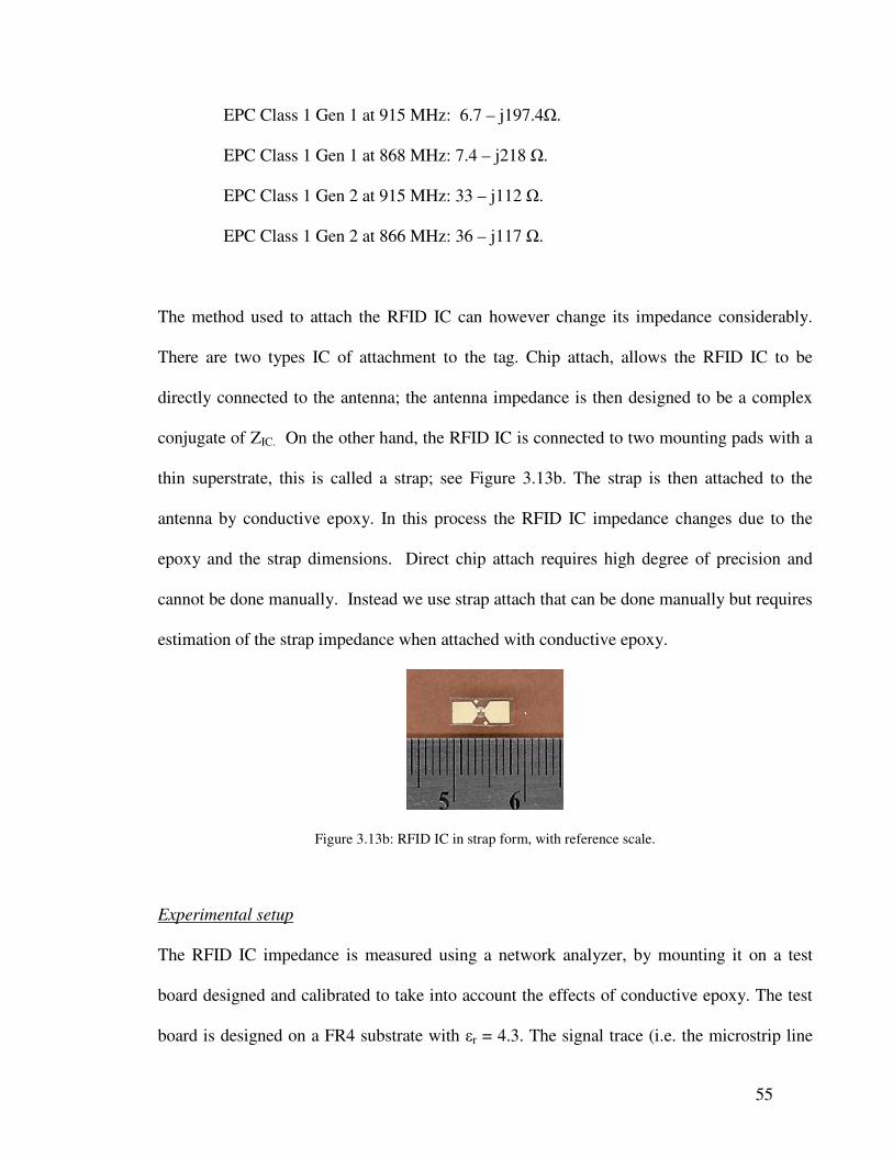
Figure 3.13b: RFID IC in strap form, with reference scale………………………………………55
Figure 3.14a: RFID strap impedance measurement board……………………………………….56
Figure 3.14b: Measured RFID IC impedance for EPC class 1 Gen 1 and Gen2………………....58
Figure 3.15: Rectangular patch antenna with balanced feed transmission lines - top view...........59
Figure 3.16: Variation in simulated patch impedance with feed position – offset.........................64
Figure 3.17: Variation in simulated port impedance with feed line width.....................................65
Figure 3.18: Total electrical length of a balanced feed microstrip antenna....................................66
Figure 3.19a: Change in simulated resonant frequency with offset................................................67
Figure 3.19b: Change in simulated resistive input impedance with offset....................................67
Figure 3.20a: Variation in input port impedance with and without shorting stub..........................69
Figure 3.20b: Variation is measured resonant frquency with finite ground plane extensions......71
Figure 3.21: Simulation model of the single patch dual stub matching networkdesign – top view........................................................................................................74
Figure 3.22: Simulation model of the single patch single stub matching networkdesign – top view........................................................................................................76
Figure 3.23: Comparision of gains for different matching networks.............................................77
Figure 3.24 : Comparision of reflction coefficient for different matching networks.....................77
Figure 4.1a: Planar microstrip antenna with balanced feed mechanism – Prototype…………….81
Figure 4.1b: Odd mode current distribution on patch antenna with balanced feed………………82
Figure 4.1c: Even mode current distribution on patch antenna with unbalanced feed…………...82
Figure 4.1d: Effect of balanced and unbalanced feed mechanisms on antenna gain…………......83

11
Figure 4.1e: Measurement prototype with single unbalanced feed connected to a SMAconnector…………………………………………………………………………….85
Figure 4.2: Simulated and measured prototype antenna input impedance with single feedexcitation…………………………………………………………………………….85
Figure 4.3 Simulated and measured prototype antenna gain characteristics……………………..87
Figure 4.4a: Avery metal tag……………………………………………………………………..91
Figure 4.4b: Avery triflex ………………………………………………………………………..91
Figure 4.4c: Symbol RFX3000 with foam backing………………………………………………91
Figure 5.1: Simulation model for dual patch direct feed broadband design..................................96
Figure 5.2: Simulated gain vs frequency – Direct feed.................................................................96
Figure 5.3: Simulated reflection coefficient vs frequency – Direct feed......................................97
Figure 5.4: Simulation model for dual patch direct feed tri- resonant broadband design............98
Figure 5.5: Simulated gain vs frequency – Tri – resonance..........................................................98
Figure 5.6: Simulated reflection coefficient vs frequency – Tri – resonance...............................99
Figure 5.7: Simulation model for dual patch inductive feed broadband design............................100
Figure 5.8: Simulated gain vs frequency – Inductive feed............................................................101
Figure 5.9: Simulated impedance vs frequency – Inductive feed.................................................101
Figure 5.10: Simulation model for dual patch combined feed broadband design.........................103
Figure 5.11: Simulated gain vs frequency – Combined feed.........................................................103
Figure 5.12: Simulated reflection coefficient vs frequency – Combined feed..............................104

12
List of Tables
Table 2.1: RFID system block representation taken from RFID handbook [5]…………………20
Table 3.1: Measured substrate properties……………………………………………………….54
Table 3.2: Notations used for antenna parameters………………………………………………60
Table 3.3: Initial design parameter values for microstrip antenna with balanced feed…………72
Table 3.4: Single patch dual stub matching network design parameter values…………………74
Table 3.5: Single patch dual stub matching network design parameter values…………………76
Table 4.1: Performance characteristics of prototype antenna…………………………………...88
Table 4.2: Performance comparison between prototype and commercial tags…………………91
Table A1: Frequency band of RFID operation in different countries………………………….114
Table A2: FCC frequency hopping table……………………………………………………...115
Table A3: ETSI Frequency hopping table…………………………………………………….116

13
1.Chapter 1
Introduction
Auto–ID (automatic identification) technology enables identification and tracking of assets
and goods. RFID (Radio frequency identification) has evolved in the recent years as a near
ideal implementation of Auto–ID. Most UHF (ultra high frequency) RFID tags are dipoles
or some variation of it and thus have characteristics similar to that of a dipole. Dipoles
suffer performance degradation when placed near conductors, e.g. metals and high dielectric
materials like water. The performance of current RFID tags is therefore limited near such
materials. We call this the ‘metal-water’ problem. Microstrip antennas offer a potential
solution to the metal-water problem. The traditional microstrip antenna design principle of a
single unbalanced feed requires cross–layered structures. The designs proposed so far based
on Planar inverted F (PIFA) [1, 2, 3] are constructed using shorting walls or vias and
therefore are of limited commercial viability due to manufacturing complexity and
associated costs. The research motivation for this thesis is to determine weather a microstrip
antenna that is completely planar can be designed.
This thesis describes the theory, implementation, and discusses the performance
characteristics of a planar microstrip antenna with balanced feed and shorting stub matching
network. Such a microstrip antenna can be described in its working using traditional odd
mode circuit analysis. The planar microstrip antenna is a rectangular patch antenna with two

14
microstrip transmission feed lines driven 180º out of phase. The antenna is designed on a
very low profile substrate, has high performance and is cheap to manufacture.
This thesis is organized into 6 chapters. Chapter 2 deals with background of RFID and
related work. It comprises of two major parts, the first part gives a brief introduction to RFID
systems; the history of RFID, its current implementation, and standards are presented. In the
second part, basics of microstrip antenna along with some common feed techniques and
broadband designs are studied. The design of microstrip RFID tags using PIFA, and its
limitations are discussed. In chapter 3 we give a detailed description of the theory and
working of planar microstrip antenna with balanced feed. The circuit model and odd mode
analysis of the antenna are presented. Since this is the first known attempt at construction of
a balanced feed microstrip antenna, the effects of various antenna and substrate parameters
are studied in detail; an initial set of design parameter values is chosen based on theses
studies. Experimental procedures to characterize the materials used in the construction of the
planar microstrip antenna are presented. The planar microstrip antenna is designed using
these materials with the initial set of parameter values. The design is then optimized to
increase performance and reduce form-factor.
Validation of the design by prototype fabrication and experimental measurement of
performance characteristics is done and the results are presented in chapter 4. We found that
the tag performance does not follow measured gain, and there are also significant differences
between measured and simulated antenna gain. Chapter 5 discusses scope of further work

15
along with some preliminary results for broadband planar microstrip antennas with balanced
feed. The conclusions from this work are presented in chapter 6.

16
2.Chapter 2
Background and Related work
The increasing need for security and visibility of goods and assets in manufacturing
companies, and, distribution and supply chains has lead to the development of automatic
identification systems. Auto-ID and data capture procedures allow identification, data
collection, and information storage about assets and goods. Auto-ID techniques include
barcodes, lasers, voice recognition, biometrics, and RFID. An ideal Auto-ID technique is one
that enables low cost implementation of data transfer without any need for human
intervention. Barcodes succeed in this to a large extent, they are however limited in their data
storage capability and require LOS (line of sight). The RFID uses IC (integrated circuit)
technology that can store large amounts of data, and, RF communication that does not
require LOS to overcome these shortcomings. It therefore provides an attractive method of
tagging objects and tracking them.
In this chapter we will discuss the history and development of RFID. The key concepts of
RFID systems, classification of RFID technology based on its implementation and
functionality are presented. Principles of passive UHF RFID operation, its performance
characteristics and limitations are studied. Microstrip antennas offer a potential solution to
some of these limitations. The basics of microstrip antenna design are presented along with
some of the existing microstrip RFID solutions.

17
2.1. Universe of RFID
Since its first use in the1930s, RFID technology has expanded and developed into
mainstream consumer good identification and tracking application. Being technically
superior to other mechanisms like bar codes [4][5], it enables RFID tagged goods to be
detected without the need for physical contact or LOS; combined with other advantages like
increased storage, greater accuracy and reliability has made this an attractive Auto-ID
solution [5]. Over the years RFID has evolved to meet the industry needs, resulting in
numerous specifications and standards.
2.1.1. History of RFID
RFID technology although has found implementations in tracking supplies in the late 80’s it
has been in existence since 1939 when it was first used as IFF (Identify Friend or Foe). IFF
was a tag and track (i.e: to tag an object and track its movement) technique used by the
British allies to identify whether airplanes were friend or foe [8]. 1960s and 70s RFID tags
found military applications like equipment and personnel tracking [7] and some unique
commercial applications like identification and temperature sensing of cattle. However the
major development in RFID tracking came only in the 80s and 90s when industrial goods
needed counterfeit protection, shrinkage protection and tracking through the several stages in
the supply chain. RFID technology prevents theft or counterfeiting of goods thus providing
security, automatic counting of goods that enter or leave warehouses allows us to keep a
track of the stock levels. Passive UHF RFID systems are increasingly being employed in
distribution and supply chains like Wal-mart and Tesco [6]. Recently several government
agencies including US-DOD and FDA have issued mandates requiring suppliers to use RFID

18
on their products [9] [10]. Apart from the industrial applications, RFID was used for baggage
tracking and access control.
With the popularity of RFID in the industry and the proven advantage of real time tracking
of goods, several manufacturers started to use the technology, there was a necessity for
compatibility between tags and readers, and hence the focus of work shifted to setting
industry driven standards for using RFID in supply chains. EPCgobal Inc., is leading this
standardization [11].
2.1.2. Need for RFID
Auto–ID technology is implemented in several different ways, including barcodes, lasers,
voice recognition, and, biometrics. These techniques suffer from limitations like the need for
LOS with the interrogator (lasers and barcodes), low data storage capacities (barcodes), and
need for human intervention (voice recognition and biometrics). RFID was developed to
overcome these limitations. RFID provides an Auto-ID technology that can operate without
a LOS, can store large amounts of user data using integrated technology. RFID proves useful
when traceability through process or life cycles is required; data errors are high in material
identification or handling; and where business systems need more information than
automatic identification technologies like bar coding can provide [5].

19
2.1.3. Types of RFID
The main components of any RFID system are the tag, the reader and the host computer.
RFID tags can be classified into two major categories based on how a tag stores the data that
has to be identified. They are without an Integrated Circuit (IC) chip or with an IC chip. The
former is a tag that has unique patterns printed on the surface of the material that
corresponds to a certain code or data that is to be stored when read by the reader. A good
example of this is a SAW RFID – surface acoustic wave RFID which is based on the
dispersion of low speed acoustic waves from the surface of a material and on piezoelectric
effect. These tags are read only, with a unique number, which is in a way similar to bar
codes. SAW RFID systems are used in high temperatures, x-rays or gamma rays [12] and
heavy manufacturing environments [13]. The second is a type of RFID that has an IC. The
IC contains all the necessary data to uniquely identify an object. The IC derives its power
from the RF signal incident on it from the reader and communicates back to the reader. The
different classes of UHF RFID tags are discussed under Section 2.1.5
2.1.4. Implementation of RFID to asset identification and tracking
RFID system is made of three major components, the reader or interrogator, the tag or
transponder, and the host computer. The reader is connected to the host computer which is
used to program the reader and store information received from the transponder. The
transponder is placed on the object to be identified. The reader is a radio transceiver [14]
connected to transmit and receive antennas. The tag consists of an antenna and the RFID IC
that contains data. The block representation of a RFID system is shown in Figure 2.1.
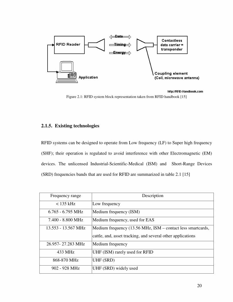
20
Figure 2.1: RFID system block representation taken from RFID handbook [15]
2.1.5. Existing technologies
RFID systems can be designed to operate from Low frequency (LF) to Super high frequency
(SHF); their operation is regulated to avoid interference with other Electromagnetic (EM)
devices. The unlicensed Industrial-Scientific-Medical (ISM) and Short-Range Devices
(SRD) frequencies bands that are used for RFID are summarized in table 2.1 [15]
Frequency range Description
< 135 kHz Low frequency
6.765 - 6.795 MHz Medium frequency (ISM)
7.400 - 8.800 MHz Medium frequency, used for EAS
13.553 - 13.567 MHz Medium frequency (13.56 MHz, ISM – contact less smartcards,
cattle, and, asset tracking, and several other applications
26.957- 27.283 MHz Medium frequency
433 MHz UHF (ISM) rarely used for RFID
868-870 MHz UHF (SRD)
902 - 928 MHz UHF (SRD) widely used
21
2.400 - 2.483 GHz SHF (ISM), vehicle identification
5.725 - 5.875 GHz SHF (ISM), rarely used for passive RFID, active tags commonly
use these frequencies
Table 2.1: RFID system block representation taken from RFID handbook [5]
RFID uses electromagnetic wave propagation to transmit and receive data. Chip based RFID
can be implemented in different ways- passive, semi-passive, active. The operating principle
for tag–reader communication is either inductive coupling between the reader and the tag or
backscattering. Inductive coupling is the transfer of energy from one device to another
through a shared magnetic field [16]. The reflection of electromagnetic waves back in the
direction from which they were received is called backscattering.
Near field RFID are based on inductive coupling between the reader and the tag. It is used
where the distance between the tag and the reader is on the order of the free space
wavelength. The magnetic field induction between the reader and tag enables
communication. Near field RFID is commonly operated in low and medium frequency
bands. Far field RFID uses backscattering
The classification of UHF RFID tags based on their operation and functionality was
developed by the Auto-ID center [17]. The layered class structure divides the tags from class
0 through class 5 as detailed below.
Class 0 are passive read only tags. They use out of band signaling [18] and use back-
scatter technique to communicate to the reader.

22
Class 1 are also passive read only tags, but they are the program-once- read-many
type tags, wherein the programming of the tag can be either done by the manufacturer
or the user, but only once. The tags use in band signaling [18] and backscattering
Class 2 are passive tags that have the additional capability of storage and encryption
[14]. Use backscattering to communicate with reader.
Class 3 are semi passive tags that have a battery source to operate the internal
circuitry. However they do not have a transmitter to send across signals to other tags /
readers. They also use backscattering for reader communication.
Class 4 tags have a battery source to supply power to the internal circuitry and have a
transmitter too. These tags are also capable of communicating with other tags that
have the same technology.
Class 5 tags, again are active, and have the additional capability of successfully
powering other IC’s of peer class and lower classes and can have two way
communication with class 4 tags. RFID readers may come under this category.
In the next section we will discuss the operating principle and performance characteristics of
UHF RFID systems.
2.2. Passive UHF RFID
Passive UHF RFID is operated in different segments of the 860-960MHz ISM band in
different countries (see Appendix – A for detailed description of frequencies of operation in

23
different countries). In section 2.1.4 we showed that electromagnetic wave propagation is
used to communicate between the tag and the reader. In passive UHF RFID systems, the
reader, primarily as a transmitter, transmits RF energy to sense the tag, a tag consisting of a
tuned antenna and a load (i.e. the RFID IC) in the far-field of the transmitter acts as a
receiver and receives the RF energy from the tag. If there is sufficient energy to power up the
RFID IC, then the tag responds to the reader. The RF energy from the reader to the tag
(forward link) is backscattered from the tag to the reader (reverse link) along with data from
the RFID IC. The ability of the tag to receive RF energy and efficiency backscatter it
depends on antenna characteristics and channel properties. The operating principles and the
typical characteristics of UHF RFID tags are detailed below.
2.2.1. Electromagnetics of RFID
The most common implementation of passive UHF RFID tag antenna is using a simple
dipole or some variation of it e.g., dual dipole, folded dipole [19] [21]. The dipole is made an
efficient radiator by designing it to be odd multiples of λ / 2 in length where, λ is the
wavelength at the central operating frequency. The tag performance, however, depends on
the radiation characteristics and the power transfer between the tag antenna and the RFID IC.

24
If an antenna is considered as a device that accepts power from one device and radiates it
into space, then the radiation efficiency of an antenna can be defined as the ratio of power
radiated into space to the total power accepted [19, 20]. It is also known as antenna
efficiency.
η*acceptedradiated PP = (2.1)
Not all the power accepted by the antenna can be radiated by it, some power is lost as it is
either absorbed by the substrate (dielectric losses) or ground (ground losses) or converted in
to heat.
A tag antenna can have good radiation efficiency and still be poor in performance if there is
considerable mismatch between the load and the antenna impedance. In RFID tags the load
is the RFID IC. A mismatch will result in RF energy being reflected back to the transmitter
without powering up the RFID IC. Therefore, it is important to match the antenna impedance
to the complex conjugate to the RFID IC impedance to achieve good power transfer from the
antenna to the load. By definition [19], the gain of an antenna (usually expressed in dBi) is
the ratio the energy radiated in particular direction when the antenna is excited with a certain
amount of input power to the theoretical isotropic antenna excited with the same amount.
Gain of the antenna takes both the radiation efficiency and the impedance match into
account. This is discussed in greater detail in chapter 3.
Assuming that the RFID system is operated in an ideal channel environment, Friis equations
[19, 21] can be used to determine the power received from the reader to the tag for a given
distance.

25
( )22
4 r
GGPP rtt
r πλ
= (2.2)
Where Pr is the power received from reader antenna to the tag antenna. It is calculated at a
distance r from the reader. The power transmitted by the reader is given by Pt. The reader
and tag antenna gains are given by Gt and Gr respectively.
In real applications however, there could be polarization mismatch (p) between the reader
and the tag antennas, and also not all power absorbed by the receiver is available to the load
due to impedance mismatch (q). Taking these factors into consideration the modified Friis
equation is written as shown in equation 2.3
( )22
4 r
GGPpqP rtt
r πλ
= (2.3)
The received power is used to both power up the RFID IC and re-radiate to the reader. The
RFID IC load varies from being nearly perfectly matched to the antenna impedance allowing
power transfer between the IC and the antenna; to a mismatched condition when all the
power is backscattered to the reader. External factors such as channel attenuation, multipath,
properties of the materials to which the tag is attached can change the overall tag
performance.

26
2.2.2. General characteristics
The performance of RFID tags vary depending on the conditions in which it is used. The
general characteristics of commercially available passive UHF RFID tags based on
performance benchmarks for passive UHF RFID tags by [14] are summarized below.
Performance in free space: Performance metric of a tag is measured in terms of the
number of times a tag responds to the reader and is detected or read by it. The
number of successful reads per unit time is defined as read rate or response rate. Most
tags perform well when measured in free space. The read rate deceases as we move
farther in distance since attenuation increases. The decrease in read rate is dependent
on Friis transmission equations. Another performance metric is the orientation
sensitivity of tags. Single dipole tags are more sensitive to orientation than dual
dipole designs due to difference in radiation patterns.
Variance in tags: Typically tags exhibit considerable variance in performance. The
lowest variance measured by [14] was nearly 3dB.
Read rates: Different protocols result in different read responses in isolation and in
population. Where isolation is defined as a condition in which only one tag is present
in the reader RF field and population means when a certain number of tags are all
simultaneously present within the reader RF field.

27
Performance near metal: Tags under go severe performance degradation when
placed in front of metal. It was observed that all tags tested would be read at 2.5mm
separation from metal. As separation increases performance improves.
Performance near water: Most tags get detuned in front of water. The tags that
perform well in free space do necessarily perform well near water. According to [14]
that all tags tested would be read at 2.5mm separation from metal. As separation
increases performance improved.
Performance near water: Most tags are de-tuned near water. Tags that perform well
in free space do not necessarily perform well near water.
The above studies [14] show that passive RFID tags are limited in performance depending
on external factors such as distance, orientation and tagged material properties.
2.2.3. Performance limitations
It was noted in the previous section that most RFID tags perform well in free space, but
undergo performance degradation when attached to different materials. This loss of
performance is because the material characteristics affect critical antenna properties such as
substrate dielectric constant and loss tangent, radiation efficiency, radiation pattern, and
radiation impedance.
High dielectric and lossy materials such as water detune the tag and reduce radiation
efficiency. Proximity to metals causes large increase in the antenna radiation resistance

28
which prevents efficient power transfer between the antenna and the RFID IC. Since metal
and water are common materials that RFID is commonly used to track, we call this the
metal-water problem. Using low dielectric materials like foam and plastics to separate metals
can improve tag performance, but it also increases thickness and manufacturing costs
significantly. Moreover, plastics that have low dielectric constant and low loss can still
detune the antenna, though modestly, by changing the substrate properties. Figure 2.2 shows
the effect of different materials on dipole far-field radiation efficiency.
Figure 2.2: Qualitative performance degradation of a UHF dipole when placed on different materials.
The tendency of RFID tags to lose performance when attached to certain materials limits its
application to tagging materials that have nearly free space properties. Unfortunately, most
assets are metal made, are encased in plastic containers or metal containers. Therefore there
is an immediate need to develop RFID tags that will have consistent performance
characteristics irrespective of the material to which it is attached.
While several attempts [23, 24, 25] have been made to create tags that perform well when
attached to metal or plastics. They are mostly, specific models that are pre-tuned to work on
different materials [24, 25]. For example a tag designed to work well near metal will still be
de-tuned when placed on plastic or near water. Or they are ordinary dipoles or some
Max Min
Air – Plastic – Glass – Water – Metal

29
variation of it encased in rugged plastic cases to shield from the effects of metal and water.
One way to achieve uniform performance with different materials is to design an antenna
that is electrically separated from the material. Microstrip antennas have a top antenna layer
a substrate and a ground plane. The ground plane separates the microstrip antenna from the
material to which it is attached. Microstrip antennas thus offer a potential the metal-water
problem of passive UHF RFID.
2.3. Literature survey of microstrip antennas
Originally implemented in 1950’s [26] microstrip antennas have since been researched
extensively. The inherent advantages like low profile, lightweight, and, low fabrication cost
[36] along with ease of fabrication and integration with other microwave microstrip devices,
has lead to numerous industrial applications for microstrip antennas. In this section the
basics of microstrip antenna along with a brief introduction to some of the feed mechanisms
and broadband techniques is presented. Recently microstrip antennas have been used to
overcome the problems associated with passive UHF RFID tags; these implementations are
discussed in Section 2.3.4.
2.3.1. Basics of microstrip antenna design
In its simplest form a microstrip antenna consists of a dielectric substrate sandwiched
between two conducting surfaces: the antenna plane and the ground plane. The simplified
microstrip patch antenna is shown in Figure 2.3.

30
Figure 2.3: Basic rectangular microstrip patch antenna construction.
Microstrip patch antennas radiate primarily because of the fringing fields between the patch
edge and the ground plane. Since the propagating EM fields lie, both in the substrate and in
free space, a quasi-TEM mode is generated. The length and width of the patch are given by a
and b respectively. The substrate thickness is given by h. When the dimension along a is
greater than b TM10 mode is the fundamental resonant mode and TM01 is secondary. If
dimension along b is greater than a then the order is reversed.
Two of the most common methods for describing the working of microstrip antennas are the
transmission line model [28, 29] and the cavity model [30, 31]. The transmission line model
is the simplest and sufficiently accurate in calculating the input impedances for simple
geometries. Its use, however, is limited by inaccuracies in prediction of impedance
bandwidth and radiation patterns, especially when thin substrates are used. The cavity model
[28, 29] assumes the antenna and ground planes to be electrical plates and the patch edges to
be surrounded by magnetic walls. This model is more accurate but computational complex
when compared to the transmission line model.
a
b
Ground
Substrate
Patch
h

31
Microstrip antenna performance is affected by the patch geometry, substrate properties and
feed techniques. One of the advantages of microstrip antennas is the freedom to choose from
a variety of patch geometries. Square patch (a = b) geometries allow both TM10 and TM01
modes to occur at the same frequency, this can be used to design λ / 4 antennas, Slight
difference between the length and width (a ≠ b) can induce circular polarization. Some of the
commonly used geometries are: square, rectangle, dipole, circle, annulus, and, triangle.
A dielectric substrate with properties such as low loss, low dielectric, and sufficiently thick
substrate can provide maximum radiation efficiency and bandwidth. However, the antenna
dimensions are large when low dielectric substrates are used. Low loss substrates provide
good radiation efficiency, but also make the microstrip antenna a high-Q device, resulting in
narrow bandwidth. The use of high dielectric substrates with higher loss gives reduced
performance, but greater bandwidth and smaller dimensions. The effects of substrate
properties on microstrip antennas and the tradeoffs involved are discussed in detail in section
3.3.
2.3.2. Feed mechanisms
A number of feed mechanisms have been developed for microstrip antennas [19, 32]. Most
often it is the feed mechanism that determines the complexity of the microstrip antenna
design. Popular feed techniques can be classified into two broad categories as follows.
• Directly connected to patch: A direct electrical connection is used to feed the
radiating patch element. E.g., microstrip line, coaxial probe.

32
Microstrip Line Feed is one of the most commonly used feed technique; a conducting
strip is connected directly to the edge of the microstrip patch. Inset feed is one in
which the microstrip line feed is inset into the patch [32] to provide the right
impedance match between the patch and the feed line; refer Figure 2.4a. The
advantage of this technique is that both the feed and the patch lie on the surface of the
substrate and therefore is planar in construction. This technique is efficient on thin
substrates; thick substrates should be avoided as they could result in spurious feed
radiation and cross polarization effects.
The Coaxial feed or probe feed has the inner conductor connected of the coaxial
cable to the patch through a hole in the substrate and the outer shield grounded by
connecting to the microstrip ground plane; see figure 2.4b. Though it is easy to place
the feed at any location on the patch, the disadvantage with this technique is it
provides narrow impedance bandwidth and is difficult to model [33, 34].
• Coupled to the patch: Electromagnetic field coupling is used to feed the patch. E.g.,
aperture coupling and proximity.
In Aperture Coupled Feed the feed line is separated from the patch by the ground
plane. Electromagnetic coupling is used to transfer power from the feed line to the
patch through a slot in the ground plane. To avoid cross-polarization the coupling
aperture is centered under the patch as shown in Figure 2.4c. It is a multi-layered

33
RadiatingPatch
Feed
SubstrateRadiatingPatch
Feed
Substrate
Substrate 2
Substrate 1
Ground plane
Aperture
Microstrip line
Patch
design, the efficiency of aperture coupling is lower compared to other techniques, but
it is easy to model [35].
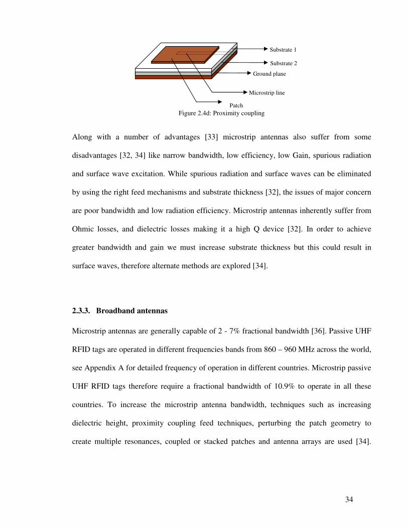
Proximity coupling feed has a feed line sandwiched between two different substrates,
see figure 2.4d. The microstrip antenna is on the top dielectric and the ground plane
is on the bottom dielectric slab. The feed line is placed between the two dielectric
slabs. The coupling is primarily capactive in nature [35].This feed mechanism
provides greater than 13% fractional bandwidth [19, 35]. The fabrication complexity
however is greater than any of the previous designs.
Figure 2.4a: Microstripline feed Figure 2.4b: Coaxial probe feed
Figure 2.4c: Aperture coupling
34
Patch
Ground plane
Substrate 2
Substrate 1
Microstrip line
Figure 2.4d: Proximity coupling
Along with a number of advantages [33] microstrip antennas also suffer from some
disadvantages [32, 34] like narrow bandwidth, low efficiency, low Gain, spurious radiation
and surface wave excitation. While spurious radiation and surface waves can be eliminated
by using the right feed mechanisms and substrate thickness [32], the issues of major concern
are poor bandwidth and low radiation efficiency. Microstrip antennas inherently suffer from
Ohmic losses, and dielectric losses making it a high Q device [32]. In order to achieve
greater bandwidth and gain we must increase substrate thickness but this could result in
surface waves, therefore alternate methods are explored [34].
2.3.3. Broadband antennas
Microstrip antennas are generally capable of 2 - 7% fractional bandwidth [36]. Passive UHF
RFID tags are operated in different frequencies bands from 860 – 960 MHz across the world,
see Appendix A for detailed frequency of operation in different countries. Microstrip passive
UHF RFID tags therefore require a fractional bandwidth of 10.9% to operate in all these
countries. To increase the microstrip antenna bandwidth, techniques such as increasing
dielectric height, proximity coupling feed techniques, perturbing the patch geometry to
create multiple resonances, coupled or stacked patches and antenna arrays are used [34].

35
Some the advantages and disadvantages of these techniques, discussed in [34] are
summarized below.
Increasing dielectric height is the simplest way to increase antenna bandwidth, but it causes
surface wave excitation and increase in antenna profile. Proximity coupled feed requires the
use of two substrates that increases overall antenna thickness and is not easy to fabricate.
Perturbation of the patch geometry is one of the most effective ways to increase antenna
bandwidth without increase in profile or form-factor. The radiating patch is designed such
that it can generate TM10 and TM01 modes at the desired frequencies. Slots in the radiating
patch can be used to meander currents and create multiple resonances. Two microstrip
patches of different lengths can be placed in proximity with each other such that they are
critically coupled and excited with a single feed. This will result in a dual band resonance.
Having two dielectric substrates with a patch on each one of them and stacking them one on
top of the other with a single ground plane at the bottom gives a stacked patch. This can be
designed to give dual or quad band resonances [36]. It however necessitates significant
increase in antenna profile. The concept of coupled and stacked patches can be extended to
more than two resonances. When larger bandwidth and increased gain are required a number
of antenna elements are connected to gather top form an array that will result in greater
aperture and consequently larger gain and bandwidth. The use of larger number of elements
however increases the antenna size.
It is evident from the above techniques that any increase the bandwidth or efficiency of a
microstrip antenna is accompanied by increase in size or thickness of the antenna.

36
2.3.4. Existing microstrip RFID designs
Researchers in the recent years have explored several microstrip antenna designs towards
RFID implementation [1, 2, 3, 27]. The inverted-F microstrip antenna forms the basis for
most of these designs. The inverted F antenna [37] is constructed by a quarterwavelength
patch terminated at on end with shorting wall or pins connecting it to the ground plane. The
patch extends from the top antenna plane with a right angle bend to the ground plane, the
ground enclosed structure looks like an inverted – F.
Planar inverted F antennas of reduced size and good performance for RFID tags were
proposed in [2, 3]. The PIFA is feed with a wire connected to the ground plane [3] as shown
in Figure 2.5, and hence is called wire-type PIFA. This type of a construction requires
imbedding the RFID IC vertically between the ground plane and the radiating patch. The
manufacturing complexity for this type of construction is significant, and prevents the design
from becoming a viable commercial solution for UHF RFID applications.
Figure 2.5: Chip attached to PIFA RFID tag [3].
An improvement to the above design was suggested by [1] in which slotted PIFA was
designed. The shorting pins are replaced with a continuous metal shorting wall that extends

37
half way into the substrate. The design has a ‘U-shaped’ slot in the patch. RFID IC is now
surface mounted, see Figure 2.6. Though this design is an improvement in some ways
compared to the wire-type PIFA, it still requires a 3-D construction.
Current RFID tag technology uses simple tag manufacturing techniques. The tag antenna is
printed or etched on an inlay, and the RFID IC is attached to the antenna. The inlay is then
attached to a substrate with adhesive. In order to be easily incorporated into such a
manufacturing process the microstrip antenna design must allow surface mounting of the
RFID IC and also be free of any cross-layered structures such as vias or shorting walls.
Figure 2.6: Slotted PIFA design with surface chip attachment [1]
The design of planar microstrip antenna with balanced feed presented in this thesis achieves
this goal. The theory and design details of this are presented in the following chapter.

38
3. Chapter 3
Implementation
Traditionally microstrip antennas are viewed as unbalanced devices. A microstrip feed is
single feed that can be designed as probe feed, microstrip line feed, or aperture feed and the
reference is always with respect to the ground plane. We reviewed some of these techniques
in chapter 2. With respect to RFID applications, the disadvantage with these feed techniques
is that they require a cross - layered construction such as a via or a shorting wall in order to
attach an RFID IC. Microstrip RFID tags discussed in Section 2.3.4 are significantly
complex and costly to construct.
In contrast, we view the microstrip antenna as capable of balanced feed. We present here a
completely planar microstrip RFID tag design. This implementation does not require any
cross-layered structures and hence greatly simplifies tag construction and consequently the
cost associated with it. The new antenna and the matching circuit design using the balanced
feed approach eliminates any reference to ground. The tag is constructed using readily
available materials that are experimentally characterized.
In the following sections we discuss the method of approach for creating a balanced feed
from two unbalanced microstrip transmission lines. Since the two lines have odd mode
symmetry, traditional odd-mode analysis is used to describe the antenna and matching
circuit. This is followed by characterization of construction materials i.e. dielectric and loss
tangent of substrate and impedance of the RFID IC. The remainder of chapter 3 discusses the

39
design parameters and the evolution of the tag design from a dual stub matching network
design to the optimized model. All simulations were done using Ansoft Designer. The
simulation results for each implementation are also presented. Bandwidth of the tag and its
form factor continue to be the limiting factors in the tag performance, these issues are
addressed towards the end of the chapter.
3.1. Balanced feed matching network design
Unlike existing techniques that use a single feed line to the microstrip patch the premise of
our approach is that we use two feeds i.e. two unbalanced transmission lines to effectively
create a single (virtual) balanced transmission line feed structure and thus eliminate any
cross- layered structures.
3.1.1. Approach
Microstrip patches offer the ability to construct antennas with the feed on a single surface by
use of microstripline feed. A microstripline feed connects to the patch either on the radiating
or the non-radiating edge and the position of the microstripline is adjusted relative to the
patch to achieve the desired input impedance (refer section 2.4.2). In the following example
we chose a single shorted tuning stub for impedance matching. Let us consider a simple
rectangular microstrip patch antenna as shown in Figure 3.1a with a single microstripline
feed that can be connect directly to an unbalanced device. The RFID IC, however, is
balanced device with two ports; each port is 180º out of phase with respect to the other.
Therefore, for a single feed design one end of the RFID IC is attached to the microstrip line

40
+ -+
Shorting Stub
while the other end is grounded using a via. The position and the length of the stub
determine the reactive component of the overall impedance.
Figure 3.1a: Single microstripline unbalanced feed Figure 3.1b: Dual microstripline differential feed
with shorting stub. with shorting stub.
Now, instead of using a single microstripline feed, we use two feeds connected
symmetrically about the vertical central axis of the patch as seen in figure 3.1b. The
differential feed to the patch antenna is achieved by using the two symmetric feed lines. The
RFID IC is connected to the two feeds. In our case, since both the feed lines need to be
matched we must either use two matching networks or simply construct a matching network
connected to both the feed lines. The shorting stub is extended symmetrically to connect
with the second feed line. Observe that figure 3.1b has E-plane symmetry. The vertical
dotted line represents the axis of symmetry. The rectangular patch is equivalent of a
transmission line with characteristic impedance ZA. Therefore the current and voltage
distributions along the patch antenna is same as that long a open ended transmission line
given by
(3.1)
(3.2)
λλπ
ofin termsdistancetheand
0atcurrenttheiswhere2
sin)(
x
xIex
IxI ojw
o =
=
0atvoltagetheiswhere2
cos)( =
= xVe
xVxV o
jwo λ
π
41
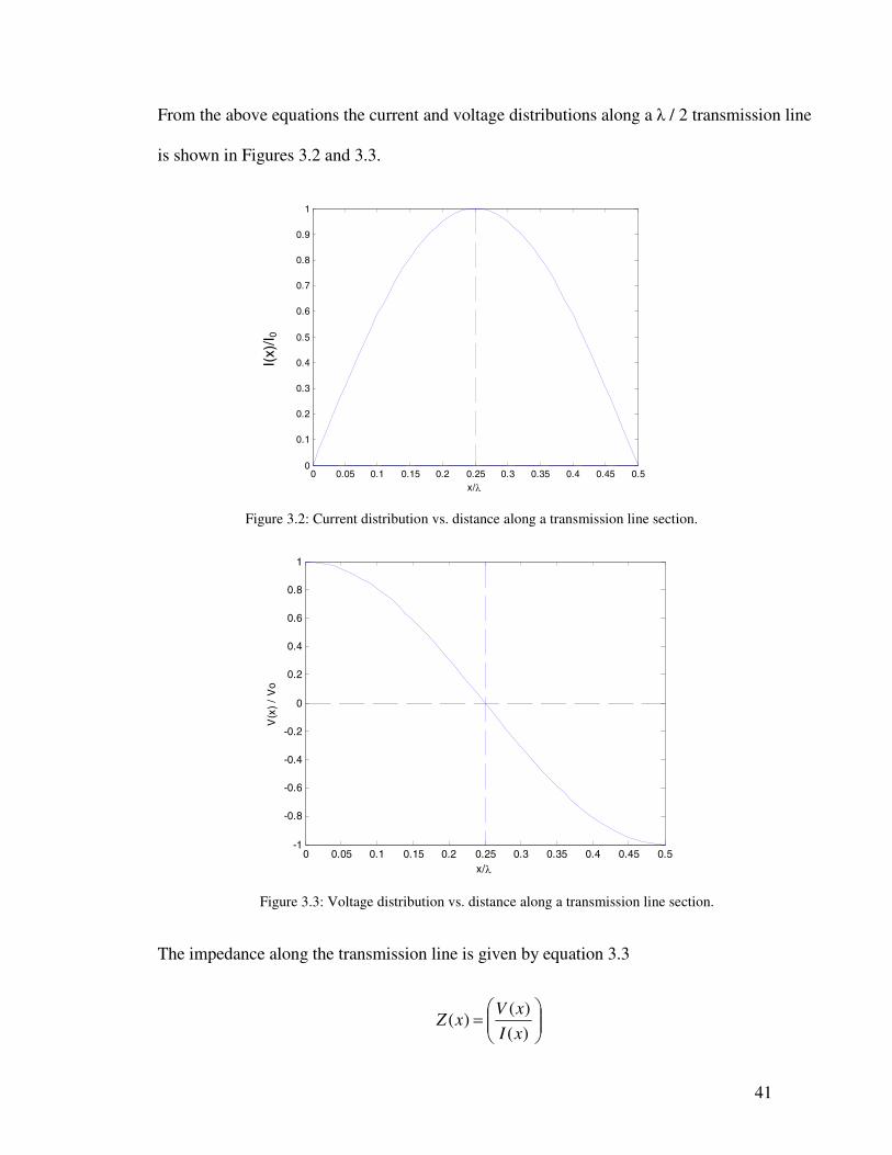
From the above equations the current and voltage distributions along a λ / 2 transmission line
is shown in Figures 3.2 and 3.3.
0 0.05 0.1 0.15 0.2 0.25 0.3 0.35 0.4 0.45 0.50
0.1
0.2
0.3
0.4
0.5
0.6
0.7
0.8
0.9
1
x/λ
Figure 3.2: Current distribution vs. distance along a transmission line section.
0 0.05 0.1 0.15 0.2 0.25 0.3 0.35 0.4 0.45 0.5-1
-0.8
-0.6
-0.4
-0.2
0
0.2
0.4
0.6
0.8
1
x/λ
V(x
)/
Vo
Figure 3.3: Voltage distribution vs. distance along a transmission line section.
The impedance along the transmission line is given by equation 3.3
)(
)()(
=
xI
xVxZ
I(x)
/I 0

42
+VI/2
L=λ/2
ZA
ZR ZR
- VI/2
The RFID microstrip tag acts as a receiver. If we consider the microstrip tag with a
rectangular patch antenna the circuit model of the rectangular patch is as shown in Figure
3.4.
Figure 3.4: Circuit model of a rectangular microstrip patch.
The total patch length is λ / 2, and, the radiating impedance is given by ZR. Since the patch is
considered to receive RF energy from the reader, the induced voltage on the patch is
represented by VI. From equations 3.2, 3.3 and 3.4 we that at x = λ / 4 the impedance goes to
zero creating a virtual ground at the center of the rectangular patch. Combining the facts that
the microstrip antenna with a balanced feed matching network has E-plane symmetry (refer
Figure 3.1b) and that the line of symmetry at x = λ / 4 is a virtual ground, (Figure 3.2 and
3.3) even-odd mode analysis can be used to describe the working of the antenna and the
matching network.
Circuit analysis
From figures 3.1b and 3.4 we observe that the patch antenna has E-plane symmetry and is
represented by two sections of λ / 4 length transmission line sections. In order to make the
43
circuit completely symmetric about the vertical axis the induced voltage is divided into two
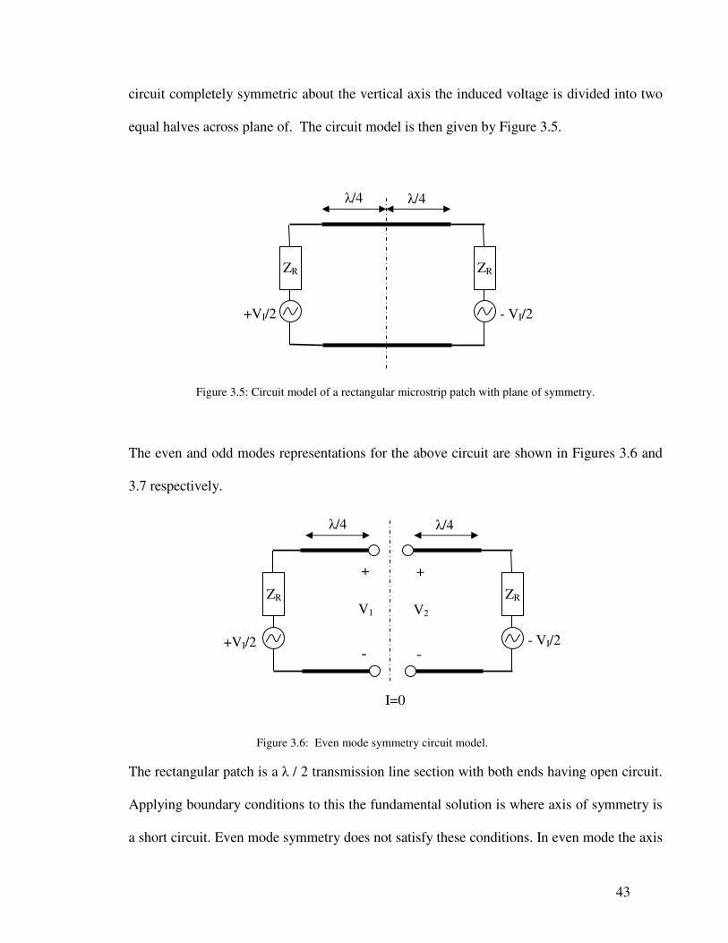
equal halves across plane of. The circuit model is then given by Figure 3.5.
Figure 3.5: Circuit model of a rectangular microstrip patch with plane of symmetry.
The even and odd modes representations for the above circuit are shown in Figures 3.6 and
3.7 respectively.
Figure 3.6: Even mode symmetry circuit model.
The rectangular patch is a λ / 2 transmission line section with both ends having open circuit.
Applying boundary conditions to this the fundamental solution is where axis of symmetry is
a short circuit. Even mode symmetry does not satisfy these conditions. In even mode the axis
+VI/2
+
-
V1
+
-
V2
ZR ZR
- VI/2
λ/4 λ/4
I=0
+VI/2
ZR ZR
- VI/2
λ/4 λ/4

44
of symmetry is an open circuit. The current flow due to even mode does not contribute to the
radiation of the rectangular patch. The voltages V1 and V2 are both equal to zero. The even
mode is therefore trivial. Also we now from the current and voltage distributions that the
axis is symmetry is a short circuit. Therefore odd mode analysis alone is sufficient to
describe this circuit.
Figure3.7: Odd mode symmetry circuit model
In the Odd mode the plane of symmetry is now a virtual ground. The voltage V1 is equal to
VI / 2 and V2 is equal - VI / 2. We can now extend the plane of symmetry to the matching
circuit and the load. Thus the circuit can be completely described using odd mode analysis
alone.
3.1.2. Odd mode analysis
Odd mode analysis can be extended from the patch to the feed, the matching network, and,
the load of the microstrip antenna. We therefore introduce two ports symmetrically at a
distance of l2 from the center of the patch as shown in Figure 3.8a. If we consider the width
of the feed lines to be very small compared to the length of the rectangular patch, we can
+VI/2
ZR ZR
- VI/2
λ/4 λ/4
+
-
V1
+
-
V2
V = 0
45
- VI/2+VI/2
ZR ZR
λ/4 λ/4
l1 l1l2 l2
P1 P2
V=0
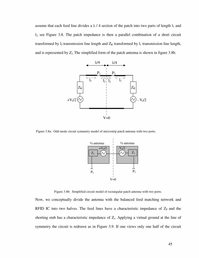
assume that each feed line divides a λ / 4 section of the patch into two parts of length l1 and
l2, see Figure 3.8. The patch impedance is then a parallel combination of a short circuit
transformed by l2 transmission line length and ZR transformed by l1 transmission line length,
and is represented by Z1. The simplified form of the patch antenna is shown in figure 3.8b.
Figure 3.8a: Odd mode circuit symmetry model of microstrip patch antenna with two ports.
Figure 3.8b: Simplified circuit model of rectangular patch antenna with two ports.
Now, we conceptually divide the antenna with the balanced feed matching network and
RFID IC into two halves. The feed lines have a characteristic impedance of ZF and the
shorting stub has a characteristic impedance of Zs. Applying a virtual ground at the line of
symmetry the circuit is redrawn as in Figure 3.9. If one views only one half of the circuit
+VI/2
P2
V=0
½ antenna ½ antenna
-VI/2
PI
Z1
+VI/2Z1

46
(Figure 3.9) with the radiation impedance, characteristic impedance of the transmission line,
line lengths, and the dashed line as a ground, it is apparent that this is a simple, single
unbalanced feed microstrip patch with single shorting stub matching circuit as seen in Figure
3.1a. We know that the load impedance is equal to the RFID IC impedance denoted by R -
jX. The total antenna impedance must then be equal to its complex conjugate R + jX.
Figure 3.9: Circuit model of microstrip patch antenna with balanced feed matching network.
The ports P1 and P2 are now defined at the end the feed transmission line; the ports are
referenced with respect to each other, instead of reference to ground; see Figure 3.10a. The
two ports are therefore combined to give one differential port. By symmetry P1 and P2 have
equal impedance. It is therefore sufficient to determine the impedance at one port. The total
impedance across P1 and P2 is twice the single port impedance. The impedance at P1 is the
patch impedance transformed by sections of feed transmission line and a shorting stub.
VI/2 Z1
Z1
-VI/2 ZL/2
½ strap
ZL/2
½ strap
½ antenna
½ antenna
ZF
ZF
Zs
Transmission lines
+VI/2

47
Figure 3.10a: Circuit model of microstrip patch antenna with two ports.
The ports divide a λ / 4 section of the patch into two sections of lengths l1 and l2; see Figure
3.8a. The impedances Z01 and Z02 are the input impedances at the end of at l1 and l2
transmission line section with ZA characteristic impedance. Z01 has zero load i.e., it is short
circuited and Z02 has a load ZR. The impedances can be calculated using transmission line
input impedance equations [38] as follows.
(3.4)
(3.5)
The impedances Z01and Z02 are in parallel and hence the total impedance is given by
equation 3.6.
Z1 = Z01 || Z02 (3.6)
½ antenna
VI/2 Z1
Z1
-VI/2
½ antenna
ZF
ZF
Zs
Transmission lines
+VI/2 P1
P2
+-
tantan
)( 102
++
==xjRZ
xjZZlxZ
rA
Ar
ββ
tan0
tan0)( 201
++
==xjZ
xjZlxZ
A
A
ββ

48
Figure 3.10b: Equivalent circuit model of microstrip patch antenna impedances.
The shunt shorting stub transforms a short circuit load by a section of transmission line
length; see Figure 3.10b. The resulting impedance of the stub is purely reactive. Assuming
the shorting stub has length of ls the input impedance Z2 is given by the following equation.
(3.7)
The circuit is further simplified as shown in Figure 3.10c.
Figure 3.10c: Equivalent circuit model of antenna and shorting stub impedances.
Thus the final impedance at port P1, called the antenna input impedance and denoted by Zin
is given by equation 3.8.
Z1
P1
Z2
ZF
ZF l3
l4
Z3
Z1
P1
ZF
ZF
ZSZ2
ltanjsββ
βtan0
tan0)(2 =
++
==xjZ
xjZlxZ
s
ss

49
+
+=
432
432in
tan)||(
tan)||(2
ZlZZjZ
ljZZZZ
F
FF β
β(3.8)
Where Z3 is given by equation 3.9.
++
=31
313 tan
tanZ
ljZZ
ljZZZ
F
FF β
β(3.9)
With known values for ZA, Zs, ZF and ZR we can determine the lengths of transmission line
lengths l1, l2, l3 and l4 required to result in a conjugate match with the RFID IC impedance.
Cross coupling effect
Balanced feed matching network design has two feed lines and a shorting stub transmission
line that lie on same plane. The coplanar nature of this design, where transmission lines are
in proximity of each other causes cross – coupling between them [38]. The effect of cross
coupling is predominantly capacitive as shown in Figure 3.10d [38, 39]. The cross coupling
capacitance is given by C12. Cross coupling between transmission lines causes change in the
characteristic impedance of transmission lines and hence the resultant port impedance.
Figure 3.10d: Cross – coupling between coplanar transmission lines [39].
Since these effects are not accounted for in the theoretical odd mode analysis using
transmission line equations, the transmission line lengths have to be manually adjusted using
simulation tools to achieve the desired impedance match.
C1 C2C12

50
3.2. Characterization of materials
In the implementation of the balanced feed matching network design for microstrip RFID
tags, one of the main considerations is to reduce construction complexity and therefore the
cost of the tag. The tag construction is as shown in Figure 3.11. The tag constitutes of a
substrate sandwiched between two metal layers; ground plane and antenna plane; the RFID
IC is attached to the antenna through a matching network. To attach to an object we remove
the bottom liner the pressure sensitive adhesive (PSA) is used to attach the tag to an object.
The tag properties are mainly dependent on thickness and dielectric constant of substrate,
antenna properties and the RFID IC impedance. Hence the first step in the implementation of
the balanced feed matching network design is the characterization of constituent materials. In
the following section the procedure for the characterization of substrate and RFID IC is
presented.
Figure: 3.11 Tag construction.
3.2.1. Dielectric of substrate
In order to minimize cost, we chose readily available plastics like high density polyethylene
(HDPE) and polypropylene (PP) for substrate material. The dielectric constant (εr) is defined

51
as the ability of a substrate to retain charge [41] and loss tangent (tanδ) is the power lost
from the patch antenna due to heating up of the substrate [42]. We use experimental methods
to determine the εr and tan δ of these materials. For a known value of εr and dielectric
thickness we can calculated the effective dielectric constant (εeff) and thus the length of
resonance of a microstrip patch of given width [32]. This principle is used to determine the εr
of HDPE and PP.
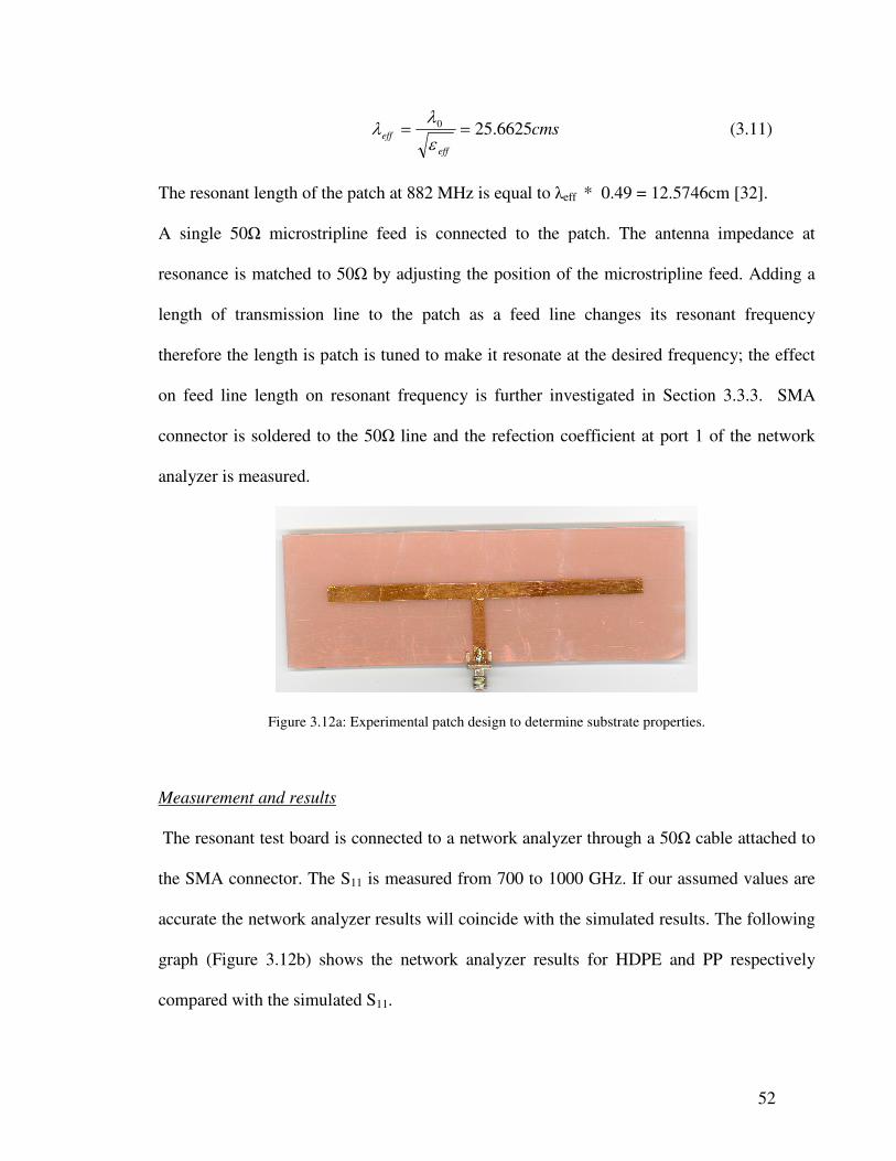
We measured the material thickness using a vernier calipers and found it to be 62 mils for
both HDPE and PP. The experimental design is based on the initial assumed values for εr
and tan δ of the materials. A test resonant patch is designed based on these assumptions. It is
experimentally tested and the measured resonant frequency is then used to estimate the
actual value of εr and tanδ.
Assumptions and Initial design
The test resonant patch is designed assuming, both materials have an εr of 2.25 and tan δ of
0.001. A microstrip patch antenna that resonates at 882 MHz is designed with the following
parameters using Ansoft Designer© simulation software. The effective dielectric constant is
given by equation 3.10 [32].
2/1
1212
1
2
1−
+
−+
+=
W
hrreff
εεε (3.10)
Where h = height of substrate and W = width of the patch. The height of dielectric is
measured to be 62mils = 1.57mm, if the patch width is 10mm and assuming εr = 2.25. Then
εeff is = 1.7334. The effective wavelength is given by equation 3.11 where λ0 is free space
wavelength for the given frequency.
52
cmseff
eff 6625.250 ==ελ
λ (3.11)
The resonant length of the patch at 882 MHz is equal to λeff * 0.49 = 12.5746cm [32].
A single 50Ω microstripline feed is connected to the patch. The antenna impedance at
resonance is matched to 50Ω by adjusting the position of the microstripline feed. Adding a
length of transmission line to the patch as a feed line changes its resonant frequency
therefore the length is patch is tuned to make it resonate at the desired frequency; the effect
on feed line length on resonant frequency is further investigated in Section 3.3.3. SMA
connector is soldered to the 50Ω line and the refection coefficient at port 1 of the network
analyzer is measured.
Figure 3.12a: Experimental patch design to determine substrate properties.
Measurement and results
The resonant test board is connected to a network analyzer through a 50Ω cable attached to
the SMA connector. The S11 is measured from 700 to 1000 GHz. If our assumed values are
accurate the network analyzer results will coincide with the simulated results. The following
graph (Figure 3.12b) shows the network analyzer results for HDPE and PP respectively
compared with the simulated S11.
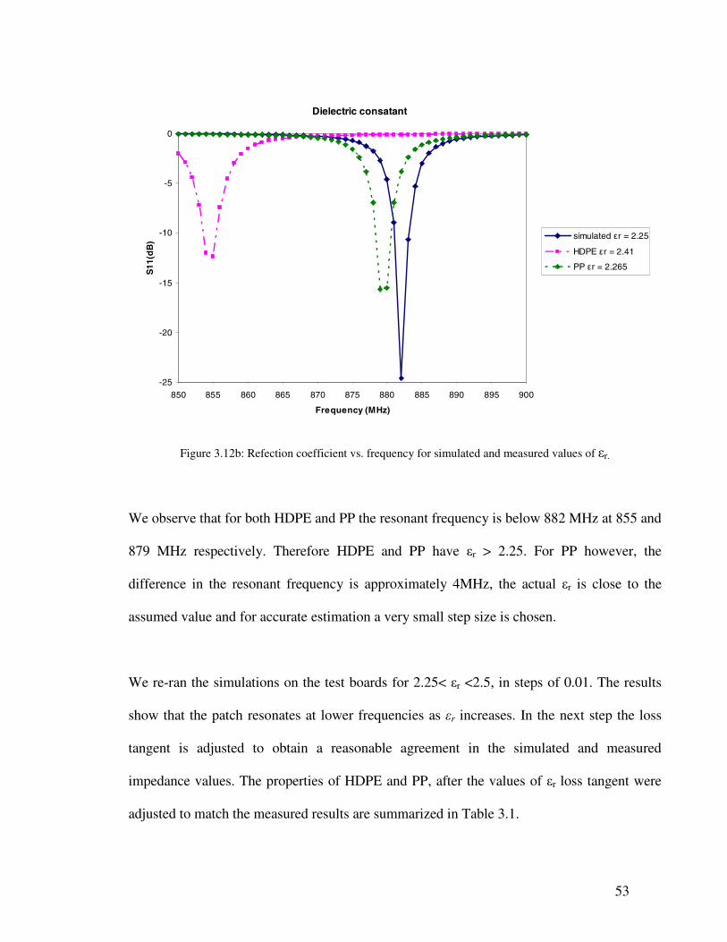
53
Dielectric consatant
-25
-20
-15
-10
-5
0
850 855 860 865 870 875 880 885 890 895 900
Frequency (MHz)
S11
(dB
)
simulated εr = 2.25
HDPE εr = 2.41
PP εr = 2.265
Figure 3.12b: Refection coefficient vs. frequency for simulated and measured values of εr.
We observe that for both HDPE and PP the resonant frequency is below 882 MHz at 855 and
879 MHz respectively. Therefore HDPE and PP have εr > 2.25. For PP however, the
difference in the resonant frequency is approximately 4MHz, the actual εr is close to the
assumed value and for accurate estimation a very small step size is chosen.
We re-ran the simulations on the test boards for 2.25< εr <2.5, in steps of 0.01. The results
show that the patch resonates at lower frequencies as εr increases. In the next step the loss
tangent is adjusted to obtain a reasonable agreement in the simulated and measured
impedance values. The properties of HDPE and PP, after the values of εr loss tangent were
adjusted to match the measured results are summarized in Table 3.1.

54
MaterialSimulated
resonance
Measured
resonanceMeasured εr Measured tanδ
HDPE 882 MHz 855 MHz 2.41 0.0035
PP 882 MHz 879 MHz 2.265 0.0012
Table 3.1: Measured substrate properties.
3.2.2. RFID IC impedance
For maximum power transfer between the tag antenna and the RFID IC, the tag antenna
impedance must be the complex conjugate of the RFID IC impedance. The RFID IC
impedance can be modeled as shown in Figure 3.13a. It is a large resistor of in parallel with
a small valued capacitor. If we assume the resistor is 2 KΩ and the capacitor is 1.2 pF then,
at the deign frequency of 915 MHz the total IC impedance is given by ZIC.
Figure 3.13a: Circuit model of the RFID IC impedance.
cIC XRZ ΙΙ= (3.12)
Where 17310*2.1*10*915*22 126
jj
Cf
jX
rc −=
−=
−= −ππ
(3.13)
1718.14
1732
j
jKZIC
−=−Ω= ΙΙ∴
(3.14)
Depending on the type of IC technology used the RFID IC impedance varies, some of the
standard chip impedances according to [39, 40] are given below.
R= 2 KΩ C = 1.2 pF
55
EPC Class 1 Gen 1 at 915 MHz: 6.7 – j197.4Ω.
EPC Class 1 Gen 1 at 868 MHz: 7.4 – j218 Ω.
EPC Class 1 Gen 2 at 915 MHz: 33 – j112 Ω.
EPC Class 1 Gen 2 at 866 MHz: 36 – j117 Ω.
The method used to attach the RFID IC can however change its impedance considerably.
There are two types IC of attachment to the tag. Chip attach, allows the RFID IC to be
directly connected to the antenna; the antenna impedance is then designed to be a complex
conjugate of ZIC. On the other hand, the RFID IC is connected to two mounting pads with a
thin superstrate, this is called a strap; see Figure 3.13b. The strap is then attached to the
antenna by conductive epoxy. In this process the RFID IC impedance changes due to the
epoxy and the strap dimensions. Direct chip attach requires high degree of precision and
cannot be done manually. Instead we use strap attach that can be done manually but requires
estimation of the strap impedance when attached with conductive epoxy.
Figure 3.13b: RFID IC in strap form, with reference scale.
Experimental setup
The RFID IC impedance is measured using a network analyzer, by mounting it on a test
board designed and calibrated to take into account the effects of conductive epoxy. The test
board is designed on a FR4 substrate with εr = 4.3. The signal trace (i.e. the microstrip line
56
that is connected to the signal pin of the SMA connector) length is kept electrically very
short at less than 8mm i.e. less than λeff /10 and has a characteristic impedance of 50Ω. The
ground pour (i.e. the copper around the signal line) is connected to the actual ground plane
by vias. A separation of 2mm is given between the signal trace and the ground pour. Two
mounting pads for the RFID IC, one form the signal line and the other from a transmission
line connected to ground (using a via) are used to mount the device under test i.e. the RFID
IC.
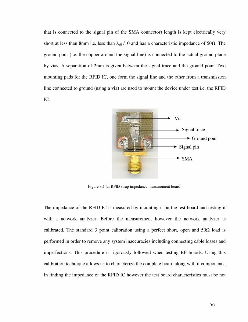
Figure 3.14a: RFID strap impedance measurement board.
The impedance of the RFID IC is measured by mounting it on the test board and testing it
with a network analyzer. Before the measurement however the network analyzer is
calibrated. The standard 3 point calibration using a perfect short, open and 50Ω load is
performed in order to remove any system inaccuracies including connecting cable losses and
imperfections. This procedure is rigorously followed when testing RF boards. Using this
calibration technique allows us to characterize the complete board along with it components.
In finding the impedance of the RFID IC however the test board characteristics must be not
Signal trace
Ground pour
Signal pin
SMA
Via

57
affect the measured IC impedance. Therefore a calibration method that allows the board
imperfections to be incorporated in the calibration itself is used.
Network analyzer is calibrated using a three point method, however the points are generated
on the test board itself instead of using the perfect open, short, and, load. The open circuit
impedance is give by the test boards without any load across it mounting pads. A copper
strip connected across the mounting pads gives a short circuit. A 50Ω resistor connect with
conductive silver epoxy is used for a standard load. The calibration is verified by placing
resistors of know value across the mounts and comparing the actual value with that measured
on the network analyzer. All resistor values were measured to be within +/- 1% of the actual
value. The RFID IC is now placed on the test board and its impedance between 860 to 960
MHz is measured.
Measurement and results
Two types of RFID straps i.e. EPC Class I Gen 1 and EPC Class I Gen 2 [22] are
characterized using the above method. The IC technology used in the two types of straps is
significantly different and therefore the measured impedances are also dissimilar. Straps of
each type were tested by manually applying a silver epoxy on the test board mount pads and
placing the strap on it. A small amount of epoxy is used inorder to prevent the strap from
being short circuited due to the spreading of the epoxy. The results for each type are
averaged. Shown below are the averaged impedance (real and imaginary) values from 860 to
960 MHz.

58
Frequency (MHz)860 870 880 890 900 910 920 930 940 950 960
-160
-140
-120
-100
-80
-60
-40
-20
0
20
40
Re (Gen2)
Img (Gen2)
Re (Gen1)
Img (Gen1)
Imp
edan
ce(o
hm
s)
Measured RFID IC impedance
Figure 3.14b: Measured RFID IC impedance for EPC class 1 Gen 1 and Gen2.
The ZIC is therefore taken to be 10 - j150 Ω for EPC class I Gen 1 straps and 35 - j110 Ω for
EPC class I Gen 2 straps.
3.3. Design parameters
In the following sections we will examine the design parameters involved in the construction
of a microstrip antenna with balanced feed matching network and how they affect antenna
performance using simulated as well as experimental results. The design parameters are
divided into two categories. Antenna parameters include substrate properties, length and
width of the rectangular patch and the microstrip feed transmission line characteristics;
matching network parameters discuss shorting stub characteristics and its position with
respect to the patch antenna.

59
It is necessary at this point to note that all the design parameters are inter-related, as we will
see in the coming sections and not all their effects on the antenna performance are fully
understood. In the last two sub-sections we present an analysis of the effect of transmission
line length and finite ground plane on resonant frequency using simulated and measured
results.
3.3.1. Antenna parameters
A microstrip patch antenna is constructed by sandwiching a layer of dielectric between two
conducting planes, the ground and the antenna. The antenna itself is made of a patch with
feed. The schematic representation of a rectangular patch antenna with balanced feed
transmission lines is shown below with parameters designated as detailed in Table 3.2
Port1
Figure 3.15: Rectangular patch antenna with balanced feed transmission lines - top view.
L
W
wF
lFoffset
x
y
z

60
Table 3.2: Notations used for antenna parameters.
The first step in designing a microstrip antenna is the selection of a substrate with suitable εr
and height. The value εr has both real and imaginary parts.
ImRe εεε jr += (3.15)
The real part accounts for charge retention, while the imaginary part accounts for the loss in
the medium. The substrate dielectric constant determines the resonant frequency of the
patch. Resonant length is inversely proportional to the square root of εr; see equation 3.11.
Thus higher dielectric constants are preferred as they result in smaller resonant lengths. But
substrates with high dielectric constants have larger losses [32]. The εr determines the
fringing fields at the patch periphery, low values of εr increases the fringing fields and thus
the radiated power [32].
If we consider that the patch and the ground plane act as two conducting plates with a
dielectric medium between them we can view the microstrip antenna as a capacitor. The
capacitance due to dielectric is given by equation 3.16.
Parameter Description Parameter Description
L Length of rectangular
patch
offset Distance of the feed line
from the radiating edge
W Width of rectangular patch lF Length of balanced feed
transmission line
wF Width of balanced feed
transmission line
tanδ Loss tangent of substrate
εr Dielectric of substrate h Height of substrate

61
(3.16)
Where εr is the relative dielectric constant, ε0 is dielectric constant of free space, ‘d ’ is the
separation between the conducting plates and is equal to the dielectric thickness h. Since the
imaginary part of εr is accounted for in the loss tangent we consider the dielectric constant
for all practical purposes to be as shown.
εRe = εr (3.17)
‘A’ is the area of the conductor plates and ‘d’ is the separation between them. The antenna
and the ground planes act as conducting plates. The Q-factor of the antenna and therefore the
antenna bandwidth depend on εr and h of substrate [32]. At higher εr the capacitance between
the two conducting planes is larger and so is the Q-factor of the antenna.
Dielectric loss (due to the substrate) along with conductor/ohmic loss (due to finite
conductivity, skin effect and roughness of metal conductors) and radiation loss constitute the
losses in a system [32, 42, 43]. The total Q-factor of an antenna is dependent on all the above
losses. Qdielectric loss is defined in equation 3.16 [43, 32]. High value of loss tangent results in
poor radiation efficiency and hence low peak gain, Q-factor is inversely related to loss
tangent [32] and hence decreases. The 3dB bandwidth defined as the difference between the
frequencies within which gain of the antenna power drops by 3dB from its peak value. As
tan δ increases the 3 dB bandwidth also increases as bandwidth is inversely proportional to
Q-factor of the antenna [38].
d
AC r 0εε=

62
δεεδ
tan
1andtan
Re
Im =−= lossdielectricQ (3.16)
After the selection of material based on εr and loss tangent, the only tunable parameter in the
substrate is the substrate thickness h. The ratio of width of patch to the dielectric height W/h
for a given εr determines the antenna Q-factor and the radiation resistance [32]. From
equation 3.16 we know that the capacitance due to dielectric depends on the dielectric
thickness. For a given εr as W/h increases (i.e., height decreases) the radiation resistance
increases and bandwidth decreases. Hence thicker substrates are preferred as they increase
radiated power, reduce conductor loss and improve bandwidth [32]. However using thicker
substrates will also increase weight, dielectric loss and surface wave loss [44]. Most high
dielectric materials also have large loss tangents. Thus for given frequency of operation,
substrates with higher values for εr result in low gain, large 3dB bandwidth and smaller size
antennas whereas, low value dielectric materials give large peak gain narrow 3dB bandwidth
and require a larger form-factor. Therefore a careful selection of substrate is critical in
determining the form-factor and the Q-factor of the antenna. We chose HDPE as the
substrate for our designs in this section as it is low cost, easy to work with, and showed
consistent substrate properties. PP samples were found to have inconsistent properties.
HDPE also has greater tan δ that gives better bandwidth compared to PP, though peak
performance is slightly reduced.
A rectangular patch offers less complexity in terms geometry. On a substrate of known εr
and height h the patch can be simply defined by L x W, where L is the resonant length
defined along the x-axis and W is the width along the y-axis. While operating in TM10 mode

63
the electric and magnetic fields vary along the length while remaining constant along the
width. Thus the length L is critical in determining the frequency of resonance. The fringing
fields the radiating ends of the rectangular patch cause radiation The patch impedance (see
equations 3.4 to 3.6) is determined by the selection of feed point position along the patch.
The microstrip feed transmission line width and length transform the actual patch impedance
as given by equations 3.8 and 3.9 and have to selected appropriately to result in a conjugate
match with the RFID IC.
A rectangular patch is essentially a microstrip a transmission line; hence the width of the
patch determines its characteristic impedance and the fudge factor [32, 36]. It is used to for
calculate the effective patch length [32, 36]. Larger patch width implies small characteristic
impedance, reduced radiation resistance, and, increased aperture. It therefore increases
radiated power, bandwidth and radiation efficiency.
At a given frequency of resonance and εr of dielectric the length L is almost always chosen
to be odd multiples of half the effective wavelength (given in equation 3.11) long to make
the patch radiate efficiently. To operate in the fundamental TM10 mode the length L is taken
to be a little less than ½ the effective wavelength in order to account for a fraction of the
fringing fields that lie outside the physical dimensions L x W [36]. The electrical length of
the antenna which is different from its physical length L is discussed in Section 3.3.3.
The position of the feed transmission line with respect to the patch determines the patch
impedance and hence the total antenna input impedance. The distance from the radiating
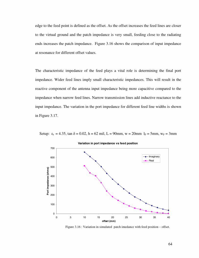
64
edge to the feed point is defined as the offset. As the offset increases the feed lines are closer
to the virtual ground and the patch impedance is very small, feeding close to the radiating
ends increases the patch impedance. Figure 3.16 shows the comparison of input impedance
at resonance for different offset values.
The characteristic impedance of the feed plays a vital role is determining the final port
impedance. Wider feed lines imply small characteristic impedances. This will result in the
reactive component of the antenna input impedance being more capacitive compared to the
impedance when narrow feed lines. Narrow transmission lines add inductive reactance to the
input impedance. The variation in the port impedance for different feed line widths is shown
in Figure 3.17.
Setup: εr = 4.35, tan δ = 0.02, h = 62 mil, L = 90mm, w = 20mm lF = 5mm, wF = 3mm
Variation in port impedance vs feed position
0
100
200
300
400
500
600
700
0 5 10 15 20 25 30 35 40
offset (mm)
Po
rtim
ped
ance
(oh
ms)
Imaginary
Real
Figure 3.16 : Variation in simulated patch imedance with feed position – offset.
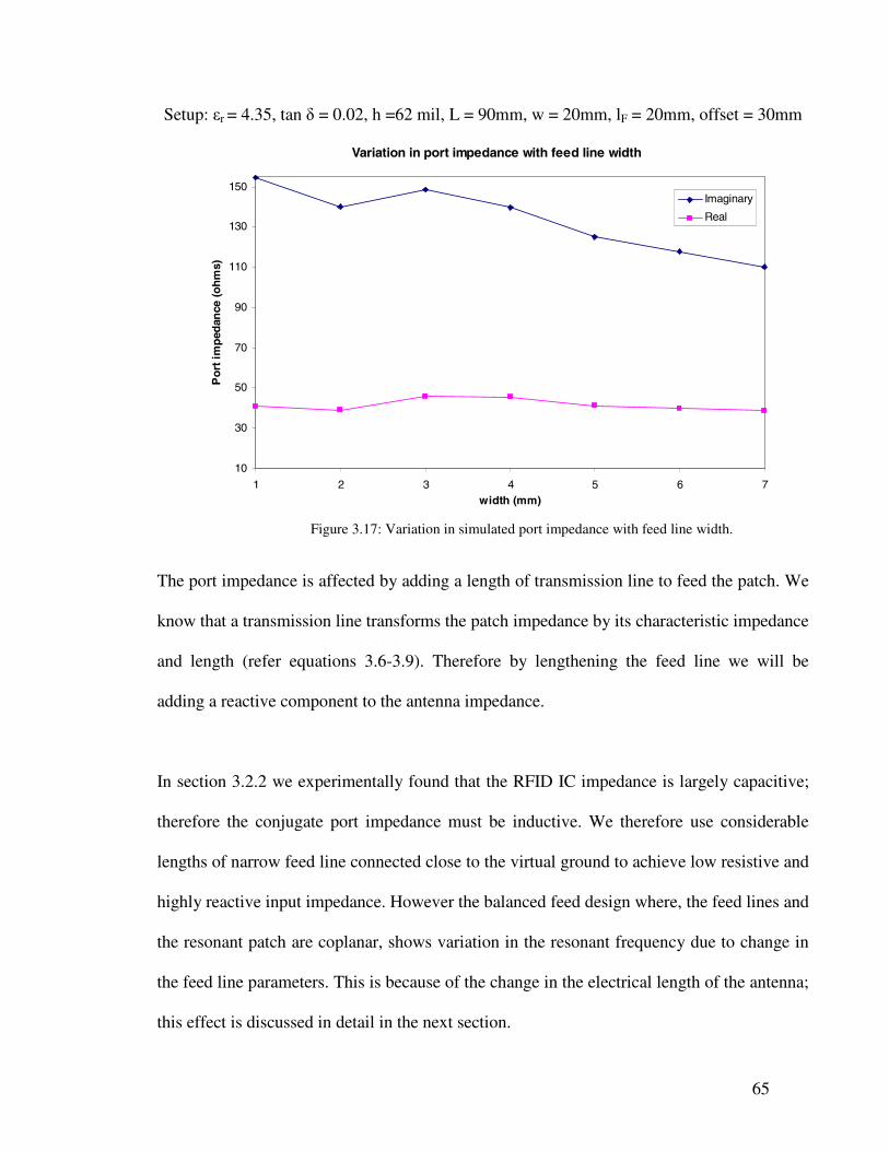
65
Setup: εr = 4.35, tan δ = 0.02, h =62 mil, L = 90mm, w = 20mm, lF = 20mm, offset = 30mm
Variation in port impedance with feed line width
10
30
50
70
90
110
130
150
1 2 3 4 5 6 7width (mm)
Po
rtim
ped
ance
(oh
ms)
Imaginary
Real
Figure 3.17: Variation in simulated port impedance with feed line width.
The port impedance is affected by adding a length of transmission line to feed the patch. We
know that a transmission line transforms the patch impedance by its characteristic impedance
and length (refer equations 3.6-3.9). Therefore by lengthening the feed line we will be
adding a reactive component to the antenna impedance.
In section 3.2.2 we experimentally found that the RFID IC impedance is largely capacitive;
therefore the conjugate port impedance must be inductive. We therefore use considerable
lengths of narrow feed line connected close to the virtual ground to achieve low resistive and
highly reactive input impedance. However the balanced feed design where, the feed lines and
the resonant patch are coplanar, shows variation in the resonant frequency due to change in
the feed line parameters. This is because of the change in the electrical length of the antenna;
this effect is discussed in detail in the next section.

66
3.3.2. Effect of feed line parameters on resonant frequency
Microstrip antennas have a narrow bandwidth and length of the antenna is critical in
determining the resonant frequency. We have seen that to operate in the fundamental TM10
mode the length L the antenna is nearly be 0.49* λeff [36], therefore, at lower frequencies the
effective wavelength is longer and hence the antenna length. In a balanced feed design
however, the total electrical antenna length is different from the physical patch length and
depends on the patch width, geometry, and, dielectric constant of substrate. By adding a feed
transmission line to the patch, we change the width of the patch at some places and
consequently its electrical length. The electrical length determines the resonant frequency.
Figure 3.18: Total electrical length of a balanced feed microstrip antenna.
Therefore, changing any of the following offset, length, or width of the feed line; will change
the effective electrical length of the antenna. Increasing offset in addition to reducing input
port impedance also reduces the electrical length making the antenna resonate at higher
frequency. Similarly lengthening the feed line adds reactive impedance and also increases
the total electrical length of the antenna thus making it resonate at a lower frequency. These
effects are illustrated in the following simulation results.
+
Port 1
_
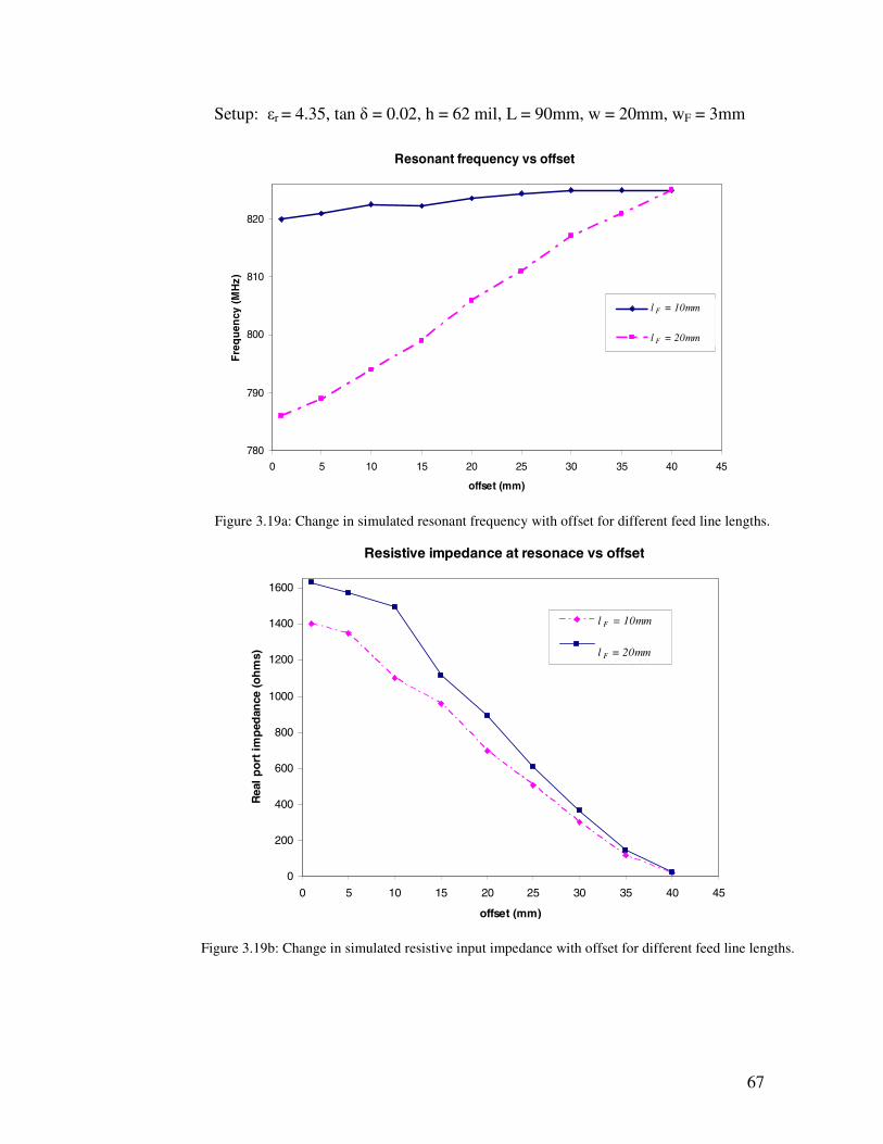
67
Setup: εr = 4.35, tan δ = 0.02, h = 62 mil, L = 90mm, w = 20mm, wF = 3mm
Resonant frequency vs offset
780
790
800
810
820
0 5 10 15 20 25 30 35 40 45
offset (mm)
Fre
qu
ency
(MH
z)
lF = 10mm
lF = 20mm
l F = 10mm
l F = 20mm
Figure 3.19a: Change in simulated resonant frequency with offset for different feed line lengths.
Resistive impedance at resonace vs offset
0
200
400
600
800
1000
1200
1400
1600
0 5 10 15 20 25 30 35 40 45
offset (mm)
Rea
lp
ort
imp
edan
ce(o
hm
s)
Impedance atresonance ΩImpedance atresonance Ω
l F = 10mm
l F = 20mm
Figure 3.19b: Change in simulated resistive input impedance with offset for different feed line lengths.

68
We simulated a microstrip patch with the above parameters and noted the variation in the
resonant frequency for different values of offset and feed line length. It is observed that for
longer lengths of lF (i.e., lF = 20mm,) the variation in the resonant frequency is greater than
when lF is smaller (i.e., lF = 10mm,). Similarly the input impedance varies from 1650
to 24 Ω at lF = 20mm, with the offset, whereas at lF = 10mm, the impedance varies between
1400 to 24Ω. As the balanced feed technique has twofold effect on the antenna
performance, some amount of manual fine tuning is necessary to obtain the impedance
match at the desired frequency. Also the feed transmission line length alone is insufficient to
provide the required reactive port impedance; we therefore use shorting stubs.
3.3.3. Matching network parameters
The purpose of a matching network is to provide impedance matching between the output
port of the source and the input port of the destination [38]. Some of the commonly used
matching network designs like quarterwave sections and multi-section transformers are
effective in matching purely resistive loads; shorting stubs can be used to match reactive
loads [38]. Since the RFID IC impedance is highly capacitive in nature the conjugate match
in predominantly inductive. In this case shorting stubs are used to add reactive impedance
rather than cancel it.
In a microstrip antenna, at resonance, the resistive impedance peaks while the reactive
impedance goes to zero. For thin substrates the resistive impedance at resonance is much
greater than reactive impedance [19]. The feed point is chosen such that the resistive
impedance is close to the value required to match 15 - j150. Placing shunt stub to the feed
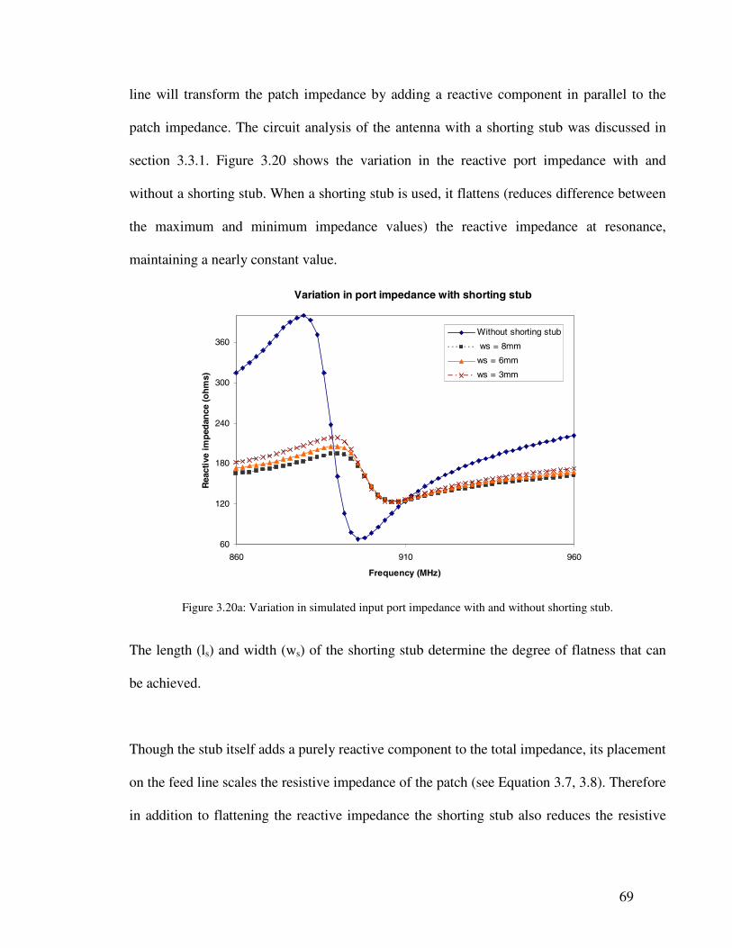
69
line will transform the patch impedance by adding a reactive component in parallel to the
patch impedance. The circuit analysis of the antenna with a shorting stub was discussed in
section 3.3.1. Figure 3.20 shows the variation in the reactive port impedance with and
without a shorting stub. When a shorting stub is used, it flattens (reduces difference between
the maximum and minimum impedance values) the reactive impedance at resonance,
maintaining a nearly constant value.
Variation in port impedance with shorting stub
60
120
180
240
300
360
860 910 960
Frequency (MHz)
Rea
ctiv
eim
ped
ance
(oh
ms)
Without shorting stub
ws = 8mm
ws = 6mm
ws = 3mm
Figure 3.20a: Variation in simulated input port impedance with and without shorting stub.
The length (ls) and width (ws) of the shorting stub determine the degree of flatness that can
be achieved.
Though the stub itself adds a purely reactive component to the total impedance, its placement
on the feed line scales the resistive impedance of the patch (see Equation 3.7, 3.8). Therefore
in addition to flattening the reactive impedance the shorting stub also reduces the resistive

70
impedance considerably allowing us to connect the feed lines farther way from the virtual
ground.
3.3.4. Effect of finite ground plane
We use Ansoft Designer software tool to simulate microstrip antenna designs. Ansoft
Designer assumes that the antenna plane is backed by an infinite substrate and ground plane.
In reality the infinite ground and substrate is replaced by finite ones. A finite ground plane
and substrate affect the radiation pattern and resonant frequency of a patch antenna [32]. In
the transmission line model of microstrip antennas the radiation pattern is calculated based
on the two-slot model [32]. For a patch radiating in the TM10 mode a two slots placed along
the radiating edges are used to model the antenna. The effect of finite ground plane and
substrate are modeled by placing slots at a distance of ‘kh’ from the ground plane, where k is
as defined in equation 3.19 [32] and h is the substrate thickness. Multiplying the resulting
factors with the E-plane pattern [32] will account for the effect of ground and substrate.
rkk ε0= (3.19)
Where k0 is the free space wave number. However the radiation pattern of the antenna is not
taken into consideration and therefore not studied in this thesis.
The speed of propagation of electromagnetic waves through the antenna, and the resulting
fringing fields determine the resonant frequency of the antenna. If the ground plane and
substrate end at the patch boundary the more fringing fields will lie in free space (i.e. a lower
dielectric than the substrate) causing the patch to resonate lower than with infinite substrate
and ground planes. We experimentally analyzed the variation in resonant frequency with the
size of ground plane. A model assuming infinite substrate and ground planes was simulated.
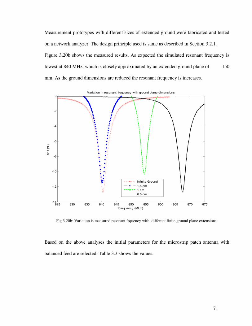
71
Measurement prototypes with different sizes of extended ground were fabricated and tested
on a network analyzer. The design principle used is same as described in Section 3.2.1.
Figure 3.20b shows the measured results. As expected the simulated resonant frequency is
lowest at 840 MHz, which is closely approximated by an extended ground plane of 150
mm. As the ground dimensions are reduced the resonant frequency is increases.
825 830 835 840 845 850 855 860 865 870 875-14
-12
-10
-8
-6
-4
-2
0
Frequency (MHz)
S11
(dB
)
Variation in resonant frequency with ground plane dimensions
Infinite Ground
1.5 cm1 cm
0.5 cm
Fig 3.20b: Variation is measured resonant frquency with different finite ground plane extensions.
Based on the above analyses the initial parameters for the microstrip patch antenna with
balanced feed are selected. Table 3.3 shows the values.

72
Parameter Value (units) Parameter Value (units)
εr 2.41 lF 10 mm
tanδ 0.0035 wF 2 mm
h 62 mils offset L/2.5 mm
L 106.6 mm ws 2 mm
W 35 mm ls 30 mm
Extended
ground plane1.5 cm
Table 3.3: Initial design parameter values for microstrip antenna with balanced feed.
The microstrip patch antenna with balanced feed is implemented with the above parameters.
Extensive simulations are used to refine the parameter values in order to achieve the design
goals, which are also described in the next section. The following section details the
implementation and optimization procedure along simulated results. A discussion of the
issues associated with the final design is also presented.
3.4. Design Evolution
The design goals for the microstrip patch RFID antenna with balanced feed mechanism
implemented in this section are to achieve peak performance at 915 MHz, with a return loss
less than -10db throughout the Federal Communications Commission (FCC) bandwidth for
RFID operations, keeping small form-factor in consideration. A stage wise implementation
procedure is adopted to arrive at the optimum values for the design parameters. The antenna
is optimized from the initial dual stub design with a large form factor to the final single stub
optimized model through a series of refinements in the parameter values.

73
3.4.1. Single patch antenna with dual stub matching network
The design is based on the parameter values specified in Table 3.3. Ansoft Designer EM
simulation tool was used to model the design. Reducing the number of variable parameters
allows us to simplify the optimization procedure, therefore for in this design we kept all
widths (patch as well as feed and matching stub transmission lines) constant. The first step in
implementation was to adjust the patch and feed line lengths to make the antenna resonate at
the desired frequency. The widths of the patch and the feed lines remained unaltered through
this. Since the offset and resonant lengths are inter-dependent, determining the feed point is
non-trivial.
The offset values are varied relative to the length of the patch. Any change in the resonant
frequency is compensated by changing the length of the rectangular patch. Offset values are
parametrically varied to achieve the correct resistive impedance. We use an EPC Class 1 Gen
1 RFID IC, which has a measured average impedance of 10 - j150. The desire port
impedance is hence the conjugate match equal to 10 + j150. Then shorting stubs are used to
tune the reactive impedance. Here the stub length and position along the feed line was
varied. It was seen that a single shorting stub of the chosen width was insufficient to
maintain high reactive input impedance. We therefore used two stubs separated by a distance
of 4mm in this design.
Since the placement of shorting stubs reduces the resistive component of the port impedance,
the offset is varied to compensate for this reduction. This procedure is repeated several times
before we arrive at the final model shown in Figure 3.21. The overall form factor of the tag
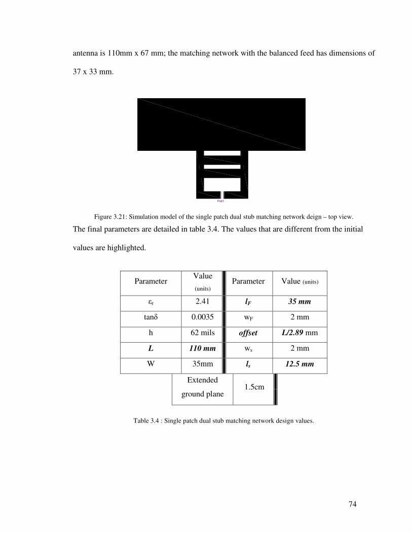
74
antenna is 110mm x 67 mm; the matching network with the balanced feed has dimensions of
37 x 33 mm.
Port1
Figure 3.21: Simulation model of the single patch dual stub matching network deign – top view.
The final parameters are detailed in table 3.4. The values that are different from the initial
values are highlighted.
ParameterValue
(units)Parameter Value (units)
εr 2.41 lF 35 mm
tanδ 0.0035 wF 2 mm
h 62 mils offset L/2.89 mm
L 110 mm ws 2 mm
W 35mm ls 12.5 mm
Extended
ground plane1.5cm
Table 3.4 : Single patch dual stub matching network design values.

75
The antenna has an impedance bandwidth that exceeds the gain bandwidth. The 3 dB
bandwidth measures 8.2 MHz. Peak gain is 0dB and occurs at 917 MHz; see Figures 3.23,
3.24.
3.4.2. Single patch antenna with single stub matching network
The single patch antenna with dual stub matching network is a good performer in terms of
impedance bandwidth; in this case defined as frequencies between which the return loss is
less tan -10dB, and, peak gain. It however, has a large form-factor. Approximately half the
total antenna size is due to the double stub matching network. The design optimization is
also partial in the sense that all line widths are unaltered from their initial assumed values. In
the second stage of design evolution the design parameter values from dual stub design are
used as a starting point for designing a new antenna and the design criteria is to minimize the
matching network area without affecting the performance. Assuming that the minimum
feature size is 1mm, the line widths are also varied, along with other parameters.
The dual stub matching network is replaced by a single shorting stub of 1mm width. The
narrow shunt stub has a characteristic impedance of 112Ω on a substrate of HDPE (εr
= 2.41). A single narrow stub with large characteristic impedance adds as much reactance as
a two lower impedance stubs in parallel. Narrow meandered feed lines also add to the
reactive impedance and also reduce the area. Since narrow feed lines will result in greater
characteristic impedance as consequently greater input impedance, the offset value is
increased and the feed lines are connected closer to the virtual ground. An EPC Class 1 Gen
2 RFID IC with measured average strap impedance 35 - j110 is attached to the antenna,
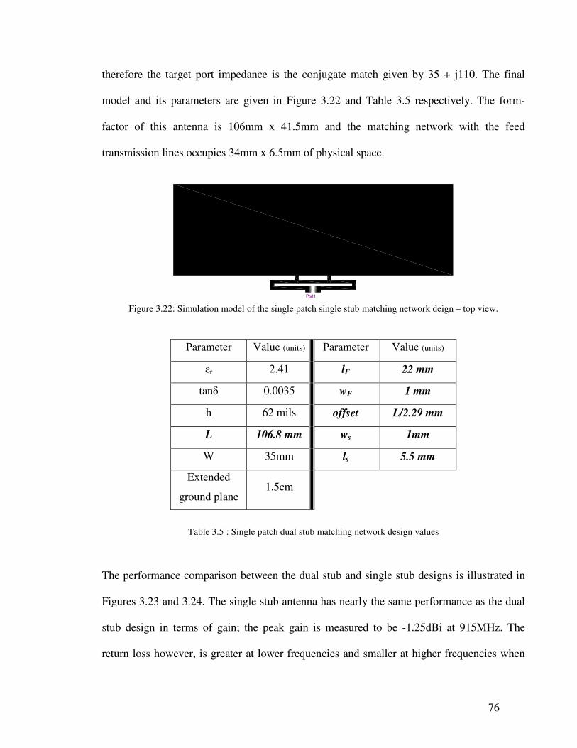
76
therefore the target port impedance is the conjugate match given by 35 + j110. The final
model and its parameters are given in Figure 3.22 and Table 3.5 respectively. The form-
factor of this antenna is 106mm x 41.5mm and the matching network with the feed
transmission lines occupies 34mm x 6.5mm of physical space.
Port1
Figure 3.22: Simulation model of the single patch single stub matching network deign – top view.
Parameter Value (units) Parameter Value (units)
εr 2.41 lF 22 mm
tanδ 0.0035 wF 1 mm
h 62 mils offset L/2.29 mm
L 106.8 mm ws 1mm
W 35mm ls 5.5 mm
Extended
ground plane1.5cm
Table 3.5 : Single patch dual stub matching network design values
The performance comparison between the dual stub and single stub designs is illustrated in
Figures 3.23 and 3.24. The single stub antenna has nearly the same performance as the dual
stub design in terms of gain; the peak gain is measured to be -1.25dBi at 915MHz. The
return loss however, is greater at lower frequencies and smaller at higher frequencies when
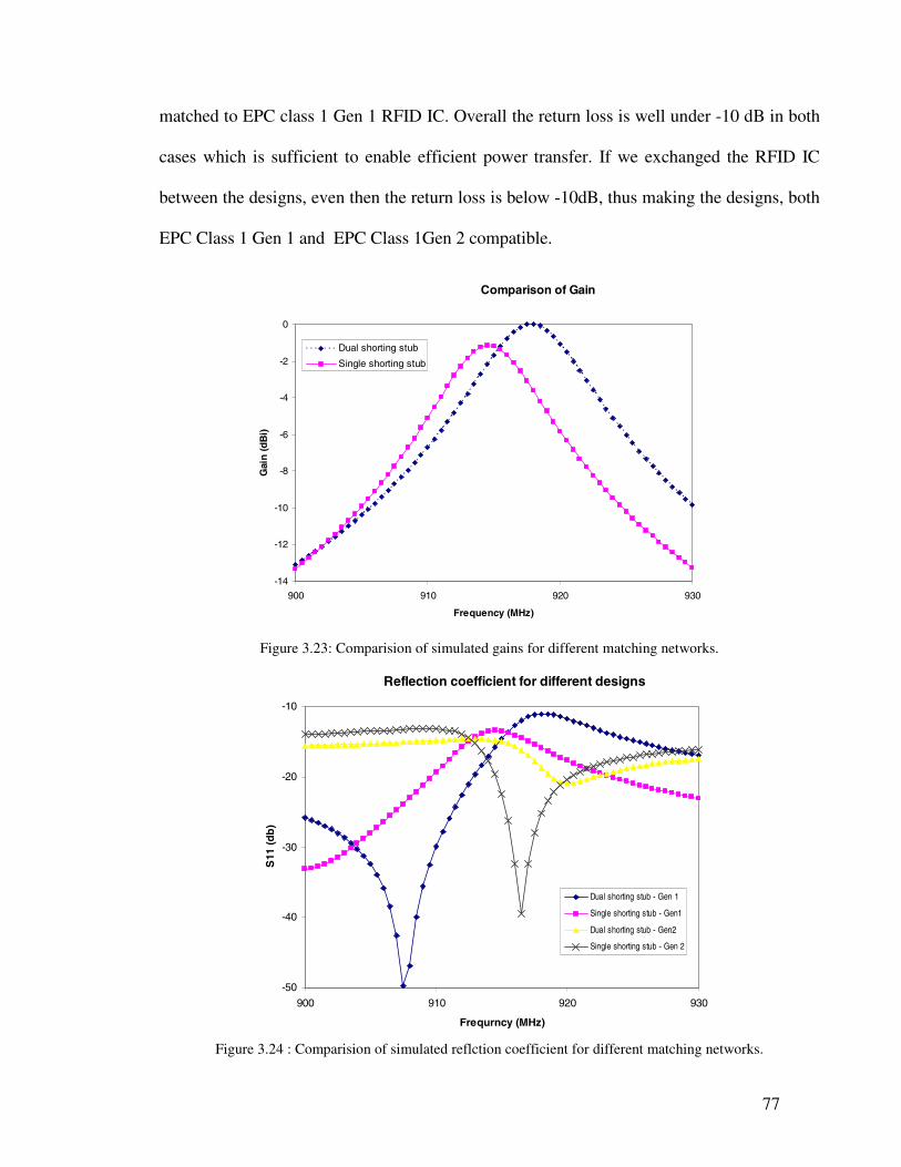
77
matched to EPC class 1 Gen 1 RFID IC. Overall the return loss is well under -10 dB in both
cases which is sufficient to enable efficient power transfer. If we exchanged the RFID IC
between the designs, even then the return loss is below -10dB, thus making the designs, both
EPC Class 1 Gen 1 and EPC Class 1Gen 2 compatible.
Comparison of Gain
-14
-12
-10
-8
-6
-4
-2
0
900 910 920 930
Frequency (MHz)
Gai
n(d
Bi)
Dual shorting stub
Single shorting stub
Figure 3.23: Comparision of simulated gains for different matching networks.
Reflection coefficient for different designs
-50
-40
-30
-20
-10
900 910 920 930
Frequrncy (MHz)
S11
(db
)
Dual shorting stub - Gen 1
Single shorting stub - Gen1
Dual shorting stub - Gen2
Single shorting stub - Gen 2
Figure 3.24 : Comparision of simulated reflction coefficient for different matching networks.

78
3.4.3. Optimization and issues
The criteria for optimization of the microstrip RFID antenna performance are
Maximize power transfer
Maximum peak performance
Minimize substrate thickness
Achieve maximum bandwidth
Minimize form - factor
The design instantiations presented in this section showed that maximum power transfer
occurred in the desired bandwidth irrespective of the RFID IC type chosen. The above
designs show that the microstrip RFID tag is gain limited while the return loss is well under -
10dB. Further investigation shows that trying to achieve minimum return loss at resonance
reduces the peak gain considerably. This is because the antenna gain is related to the
resistive component of input impedance as given in equations 3.20 and 3.21 [19].
P
rEGain
30
2
),(
),(
φθφθ = (3.20)
|rE| is the magnitude of the radiated electric field multiplied by the distance, r and P is the
power, in watts which for a single port device is calculate as
( ) ( )( )211)(
21*Re* SZIP in −= (3.21)
Where Zin is the impedance across ports P1 and P2, and S11 is the return loss and I is the
current at port one taken by default as 1 amp. Therefore matching to very low real
impedance (i.e. 10 – 35Ω as the case may be) causes high current densities resulting in larger

79
Ohmic losses [32] and reduced gain. A tradeoff is therefore established between the port
impedance at resonance and the gain. The port impedance is maximized until the threshold
of -10dB return loss maintained resulting in good power transfer while maximizing gain.
Any further increase in the real value of the port impedance will results in reduced power
transfer. The conductive losses are minimized by use of thick copper for the antenna.
The other three criteria are inter-related more difficult to achieve. The microstrip antennas
were designed on 62 mil substrate keeping the low profile of the antenna in mind. At this
substrate thickness the fractional bandwidth of the antenna is nearly 1%. Minimizing
substrate thickness to less than 62 mils will result in severe loss of bandwidth and therefore
is avoided. Similarly reducing the form–factor will result in reduce peak performance and
bandwidth due to reduced aperture.
The design prototypes presented in this section are sub-optimal realizations in terms of
bandwidth and form-factor. In order to achieve optimum performance, techniques such as
multi-resonant designs [34] with electromagnetically coupled feeds and more complex patch
geometries need to be explored. Preliminary investigation of some of these techniques is
presented in chapter 5.

80
4.Chapter 4
Results
The single stub matching network design discussed in chapter 3 is considered to be the
optimized planar microstrip antenna design with balanced feed. This design was fabricated in
the lab and its performance characteristics were experimentally measured. The prototype
validation procedure and measured results are presented in this chapter.
The original intent of this project was to demonstrate that a planar microstrip antenna for
RFID applications is possible and show that such a RFID tag will have uniform performance
irrespective of the material to which it is attached. The prototype is therefore compared with
other commercially available RFID tags near metals and water with read distance as the
comparison metric, the results are discussed towards the end of this chapter.
4.1. Measured results
The single stub matching network design was simulated using Ansoft Designer, the
simulated results were presented in Section 3.4. To validate these results, a prototype was
built and a testing procedure was developed.
4.1.1. Prototype fabrication
The Ansoft model for the optimize microstrip RFID tag was fabricated in the lab manually.
Prototype fabrication is a simple three stage process is easy to implement. Firstly the

81
substrate is cut to the required size (i.e. antenna dimensions and additional 1.5 cm of
extended ground plane). The substrate is now covered with a self adhering copper layer on
both sides. The Ansoft Designer model is cut out on one side of the substrate while the other
serves as the ground plane. The RFID IC with the strap is then attached to the antenna using
conductive silver epoxy. The epoxy used is the same that was used to test the RFID IC
impedance. A secondary adhesive layer is applied on the strap to provide mechanical
stability to the attachment. Figure 4.1a shows the prototype with a Class 1 Gen 2 RFID IC.
Figure 4.1a: Planar microstrip antenna with balanced feed mechanism – Prototype.
4.1.2. Measurement setup and results
Validation and performance measurement of this prototype involves measuring the antenna
input impedance and gain over the given bandwidth. Since the antenna is a balanced device
it is not possible to directly measure its impedance using a network analyzer. The balanced
feed has to be converted into an unbalanced feed using a device called balun. The port
impedance can now be directly measured from the balun output using a network analyzer.
Alternately, since our design has odd mode symmetry, the input impedance measured at only
one of the two balanced feed lines must be equal to ½ the overall antenna impedance; (see

82
Section 3.1 for details). That is, without using a balun, we can measure the input impedance
at the end of one feed transmission line with reference to ground. But feeding the patch with
a single balanced feed will change the current distribution on the patch and therefore the far
field pattern. The device no longer has only odd mode, an even mode is also present as
shown in Figure 4.1b and 4.1c.
Figure 4.1b: Odd mode current distribution on Figure 4.1c: Even mode current distribution on
patch antenna with balanced feed. patch antenna with unbalanced feed.
Notice that in Figure 4.1b the balanced feed lines have currents flowing in opposite
directions. In Figure 4.1c, only one the feed lines is used to create a port. The current from
this feed line through the shorting stub reaches the non – excited feed line. The current here
splits in two direction one in the same direction as the current flow in the excited feed line,
the other, is in the opposite direction. Thus both even and odd modes exist when unbalanced
feed is used.
The even mode, however, does not contribute substantially to the far field radiation at the
frequencies in which the device is required to operate. This is shown by simulating the
antenna with two ports excited 180 out of phase with each other (i.e., balanced feed) and
with a single port excited with reference to ground (i.e., unbalanced feed). The simulated
+
Port 1
++
Port 1
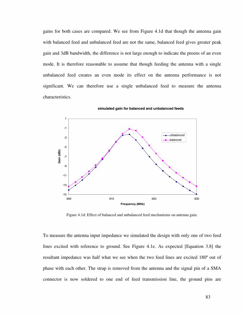
83
gains for both cases are compared. We see from Figure 4.1d that though the antenna gain
with balanced feed and unbalanced feed are not the same, balanced feed gives greater peak
gain and 3dB bandwidth, the difference is not large enough to indicate the preens of an even
mode. It is therefore reasonable to assume that though feeding the antenna with a single
unbalanced feed creates an even mode its effect on the antenna performance is not
significant. We can therefore use a single unbalanced feed to measure the antenna
characteristics.
simulated gain for balanced and unbalanced feeds
-15
-13
-11
-9
-7
-5
-3
-1
1
900 910 920 930
Frequency (MHz)
Gai
n(d
Bi)
unbalanced
balanced
Figure 4.1d: Effect of balanced and unbalanced feed mechanisms on antenna gain.
To measure the antenna input impedance we simulated the design with only one of two feed
lines excited with reference to ground. See Figure 4.1e. As expected [Equation 3.8] the
resultant impedance was half what we see when the two feed lines are excited 180º out of
phase with each other. The strap is removed from the antenna and the signal pin of a SMA
connector is now soldered to one end of feed transmission line, the ground pins are
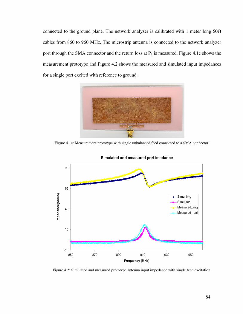
84
connected to the ground plane. The network analyzer is calibrated with 1 meter long 50Ω
cables from 860 to 960 MHz. The microstrip antenna is connected to the network analyzer
port through the SMA connector and the return loss at P1 is measured. Figure 4.1e shows the
measurement prototype and Figure 4.2 shows the measured and simulated input impedances
for a single port excited with reference to ground.
Figure 4.1e: Measurement prototype with single unbalanced feed connected to a SMA connector.
Simulated and measured port imedance
-10
15
40
65
90
850 870 890 910 930 950
Frequency (MHz)
Imp
edan
ce(o
hm
s) Simu_img
Simu_real
Measured_Img
Measured_real
Figure 4.2: Simulated and measured prototype antenna input impedance with single feed excitation.

85
trr GG
r
GS ==
)4( 2
222
21 Θπλ
2/1
2
22
21
)4(
=
λπr
SGr
2
21SP
P
t
r =
The above results show that there is good agreement between simulated and measured
impedance values. The lower resistance values are nearly equal to zero in simulation, but,
measurement shows that they are slightly below zero which in reality is not possible. Since
the actual value itself is very small this error is ignored. Since both simulated and measured
peaks occur at almost the same frequency and are of equal value it validates our estimates of
dielectric constant and loss tangent. The Q-factor of the antenna is as expected. The
experimental method used for characterization of substrate materials is therefore accurate.
The gain of the prototype antenna is measured in two different ways. Firstly two prototype
antennas are fabricated and tested for input impedance and resonant frequency. Having
confirmed that they have similar impedances and resonant frequencies we assume that they
will also have similar gains. One antenna treated as the transmitter. It is connected to one of
network analyzer ports. The other treated as the receiver is connected to second port of the
network analyzer. The ratio of the power transmitted from transmitter antenna to the power
received by the receiver antenna is then proportional to the magnitude squared of S21.
(4.1)
Friis equation can then be re-written as shown.
(4.2)
The antenna gain is then calculated as follows.
(4.3)

86
In an alternate method the prototype is tested in real RFID environment with a
programmable RFID reader. The prototype with the RFID IC attached to it is placed in front
of the reader antenna at a fixed distance. The reader antenna (transmitter) and the prototype
(receiver) have a clear line of sight path. The RFID reader in general is continually hopping
i.e., changing frequencies randomly (see Appendix – A for additional information) to
different frequencies in the given FCC frequency band. The maximum power for FCC
frequency of operation is 36dBm [45]. The reader frequency and its output power can be
controlled by setting the appropriate registers in the RFID reader. In testing the prototype
tag the RFID reader was programmed to frequency sweep starting from 902.3 MHz to 927.3
MHz in steps of 1 MHz. At each frequency step the output power from the reader is reduced
from a maximum allowable of 36 dBm until is reader stops reading the prototype tag. The
least reader power at which the tag is read is taken to be the transmit power of the RFID
reader that is required to power up the RFID IC.
We assume that the received power from the reader to the tag is the minimum that is required
to turn the RFID IC on and is equal to 6.5µm. The RFID transmit antenna is circularly
polarized, therefore 3dBi is subtracted from the actual transmit antenna gain to account for
the polarization mismatch. Since the RFID IC impedance is matched to the antenna input
impedance with less than -10db return loss, we assume that there is no impedance mismatch.
Channel conditions are also assumed to be ideal. Using Friis equations we can calculate the
receiver antenna gain at each frequency step using the following parameters.
Transmitted power = tP = minimum reader power required to turn on the RFID IC.
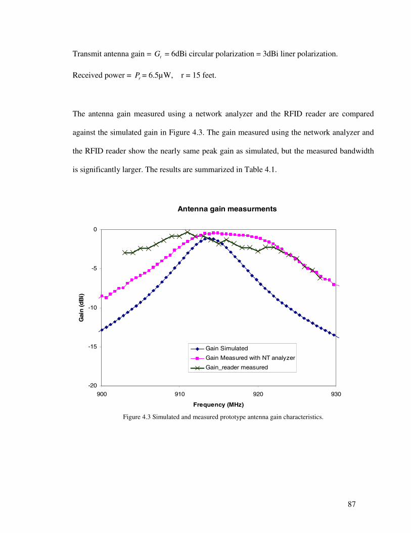
87
Transmit antenna gain = tG = 6dBi circular polarization = 3dBi liner polarization.
Received power = rP = 6.5µW, r = 15 feet.
The antenna gain measured using a network analyzer and the RFID reader are compared
against the simulated gain in Figure 4.3. The gain measured using the network analyzer and
the RFID reader show the nearly same peak gain as simulated, but the measured bandwidth
is significantly larger. The results are summarized in Table 4.1.
Antenna gain measurments
-20
-15
-10
-5
0
900 910 920 930
Frequency (MHz)
Gai
n(d
Bi)
Gain Simulated
Gain Measured with NT analyzer
Gain_reader measured
Figure 4.3 Simulated and measured prototype antenna gain characteristics.

88
Method Peak Gain (dBi) 3dB bandwidth (MHz)
Simulated -1.25 10.3
Measured with
network analyzer-0.48 15.8
Measured with
RFID reader-0.33 20.6
Table 4.1: Performance characteristics of prototype antenna for different measurement techniques.
While the simulated gain and gain measured with network analyzer differ by 5.5 MHz; the
reader measured gain is nearly twice that simulated. The possible reasons for the difference
between the simulated and measured values are discussed below.
The experimental setup to find the dielectric loss tangent of substrate material was
inaccurate. If the actual loss tangent is greater than that measured, the Q of the
antenna is reduced resulting in greater bandwidth. This may not be true due to fact
that the peak gains are still nearly equal. A greater loss tangent must result in reduced
peak gain.
It is quite possible that the antenna has more than one resonance in the desired
frequency band due to ground plane resonance i.e., when the ground plane itself acts
as a patch and resonates or dielectric resonance i.e., the dielectric cavity between the
two conducting planes resonates. This is verified by placing the prototype on a larger
sheet of metal and measuring the gain. The results are similar to those obtained
previously. This eliminates the possibility of dual resonances.

89
Since the RFID IC in strap form is attached to the antenna by conductive epoxy, there
is possibility of capacitive coupling between the strap and the antenna. This
capacitive bonding between the strap and the antenna could result in increased
bandwidth.
The presence of multipath and ground reflection is ignored in the measurement of
prototype antenna gain using both network analyzer and the RFID reader. The
measurement was therefore repeated in different physical locations. The results were
found to largely coincide with those previously measured. Therefore the effect of
channel properties though present, does not account for the increase in the bandwidth
of the antenna.
The reader antenna is assumed to have constant gain over the desired frequency band.
A possible variation in the gain with frequency could account for the difference
between the gain measured using the network analyzer and the reader antenna. Also
any non-linearities in the RFID IC is neglected while measuring with RFID reader.
Ansoft Designer software tool that is used to simulate these models makes some
assumptions in the way it models the antenna design. Anosft Designer assumes an
infinite ground plane and substrate over which the patch is created. The Method of
Moments (MoM) [46, 47] is used to solve for the electromagnetic (EM) fields of the
antenna. This method uses surface waves to model the microstrip patch and
polarization currents to model the substrate. The above mentioned assumptions along
with the method of computing antenna EM fields could account for deviation of
measured gain from simulated gain.

90
The primary objective of this thesis is to demonstrate that the balanced feed microstrip
RFID tag will solve the metal-water problem associated with current passive UHF RFID
tags. The prototype is therefore, further tested for performance near metal and water and
the results are compared against of some commercially available tags
4.2. Comparisons
The prototype tag was compared with other commercial tags in an RFID environment. The
prototype and the commercial tags were placed in free space, on metal with cardboard
separation, directly on metal, on plastic container with water and the maximum read distance
was the metric of interest. We know that when tags are placed on metal radiation resistance
increases and on high dielectric they are detuned. The extent of performance degradation is
reflected in the reduced read distance.
Several manufacturers have come up with tags that work reasonably well near metal and
water, some of these tags were chosen for comparison purposes based on availability at the
time of testing.
Avery metal tag is a dipole design with plexiglass substrate and partial metal ground
plane. The tag dimensions are 177 x 25 x 5mm. See Figure 4.4a.
Symbol RFX3000 is dual dipole design with 5mm foam backing, the overall tag
dimensions are 96 x 96 x 5 mm. See Figure 4.4b
Avery Triflex is also a dual dipole design, with only three poles. One of the poles by
symmetry acts as a common base. Tag dimensions are 97 x 107 x 0.07 mm. See
Figure 4.4c.
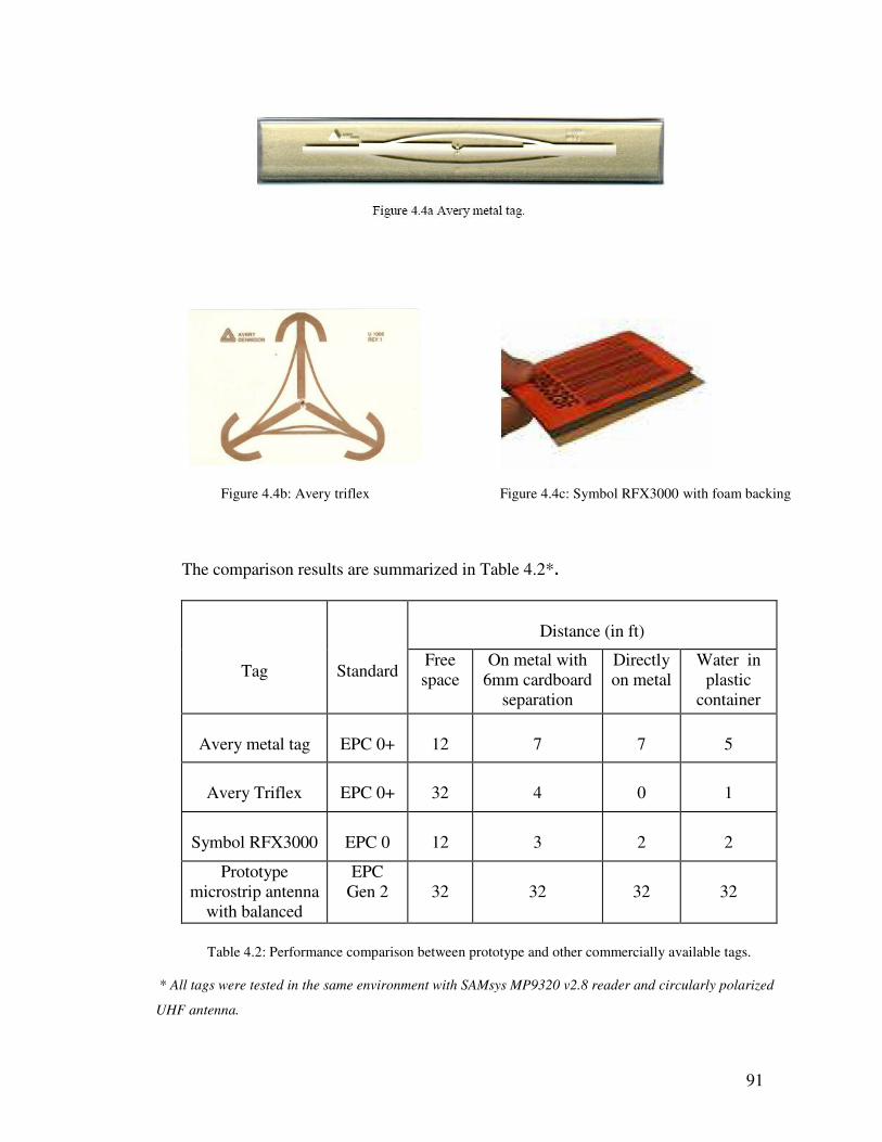
91
Figure 4.4b: Avery triflex Figure 4.4c: Symbol RFX3000 with foam backing
The comparison results are summarized in Table 4.2*.
Distance (in ft)
Tag StandardFreespace
On metal with6mm cardboard
separation
Directlyon metal
Water inplastic
container
Avery metal tag EPC 0+ 12 7 7 5
Avery Triflex EPC 0+ 32 4 0 1
Symbol RFX3000 EPC 0 12 3 2 2
Prototypemicrostrip antenna
with balanced
EPCGen 2 32 32 32 32
Table 4.2: Performance comparison between prototype and other commercially available tags.
* All tags were tested in the same environment with SAMsys MP9320 v2.8 reader and circularly polarized
UHF antenna.

92
The above comparisons show that the prototype tag has superior performance in free space
as well as near metal and water compared to other tags. The Avery metal tag comes second;
this is easily explained by the fact that the Avery metal tag itself is based on microstrip
dipole design. It is seen that attaching tags with cardboard separation to metal gives better
performance than when attached directly to metal. This is because cardboard has dielectric
constant equal to nearly that of free space and placing the tag with cardboard separation
gives reduced radiation resistance than compared to tag directly on metal, resulting in better
impedance match and therefore better read distance. Unlike other tags the prototype does not
lose any performance in the presence of metal or water.

93
5.
Chapter 5
Future work
The balanced feed matching network microstrip antenna is a potential solution to the metal-
water problem of RFID. The results from chapter 4 however show that the single patch
single shorting stub design is limited in its performance by narrow gain bandwidth. The
constraint to keep the microstrip RFID tag low profile and cost effective, eliminates the
possibility of making use of traditional broadband techniques such as proximity coupling,
thick substrates, and, stacked patches. The scope of future work lies in exploring planar
mechanisms that would allow us to increase the gain bandwidth and reduce the form factor.
One of the possible techniques is to use multiple, narrow rectangular patches of different
lengths to create multiple resonances at the desired frequencies. This however necessitates
the increase in the form factor due to the presence of two patches and consequently two
matching networks.
In this chapter we investigate some of novel feed mechanisms and coupling techniques that
will allow us to use a 2 element planar microstrip antenna array that extends the bandwidth
of the antenna without necessitating any increase in substrate thickness or the form factor of
the antenna. Simulation results are also presented. While the 2 element array resolves the
bandwidth issue to an extent, the large form factor issue remains. Towards the end of this
chapter design techniques using meandered patch geometries, capable of multiple modes
[32] for multi-resonance are suggested to reduce the form factor while simultaneously

94
increasing the bandwidth. There is also a need to study the effects of balanced feed
mechanism on a microstrip patch and create mathematical models that could describe the
relation between antenna performance and feed parameters, and allow optimization based on
derived theoretical limits.
5.1. Broadband designs
5.1.1. Dual patch broadband antenna design
The simplest way to create a broadband antenna is to make an array of elements [34] that
will couple and resonate at different intervals in the desired frequency band, providing an
overall 3dB bandwidth that is greater when compared to that of a single resonating element.
The antenna array construction is very similar to that of a single element patch expect for the
feed mechanism. The feed structure is now constructed such that it couples to both elements
and provides an impedance bandwidth that is greater than or equal to the gain bandwidth of
the array. The antenna is excited either by means of dual transmission lines that form a
balanced feed structure or by means of inductive couple feed. The feed mechanisms can be
classified into three categories as follows.
Direct balanced feed
Inductively coupled feed
Combined inductive and direct feed
The dual patch microstrip antenna design is often capable of dual resonance and in some
cases can give rise to multiple (tri or quadruple) resonances. Some of the design
instantiations based on the above feed methods with EPC Class 1 Gen 2 RFID IC with 62

95
mil polypropylene (PP) substrate, εr = 2.265, tan δ = 0.0035 are discussed below. We choose
polypropylene for these designs as we know that it has very low loss tangent and therefore is
a high Q- factor device. The idea is to see by what amount, the 3dB bandwidth of a high-Q
antenna can be increased using the above mentioned techniques.
Dual patch direct balanced feed: The fundamental concept of a balanced microstrip feed to
a rectangular patch is extended to two rectangular patches in this example. The design
consists of two patches, coupling between which plays an important role in determining the
resonant frequencies and the overall bandwidth of the array. Spacing the array elements too
far results in under coupling, narrow gaps could result in over coupling and the antenna
efficiency is reduced in both cases.
While critical coupling between array elements is important, the design of the matching
network also affects the resonant frequency (Refer section 3.3.2). We therefore create two
matching networks allowing greater degree of freedom in design. The design uses two
patches with dissimilar dimensions; each having a pair of differential feed transmission lines
connecting it to the RFID IC through a single shorting stub matching network. Figure 5.1
shows the simulation model of the dual patch direct feed design. The overall dimensions of
the antenna are 112mm x 49mm and it is implemented on PP substrate. The antenna array
has two operating frequencies corresponding to 914 MHz and 926 MHz. The antenna has a
3dB BW of 4.2 MHz from 911.7 to 915.9MHz and 4 MHz from 924.5 to 928.5 MHz. The
overall BW is hence equal to 8.2 MHz i.e. twice the bandwidth of a single resonant patch
with same substrate.
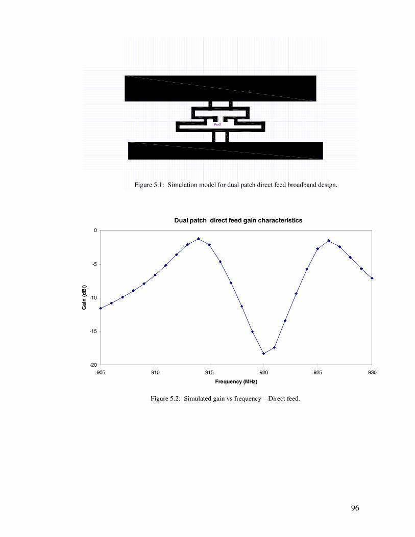
96
Port1
Figure 5.1: Simulation model for dual patch direct feed broadband design.
Dual patch direct feed gain characteristics
-20
-15
-10
-5
0
905 910 915 920 925 930
Frequency (MHz)
Gai
n(d
Bi)
Figure 5.2: Simulated gain vs frequency – Direct feed.
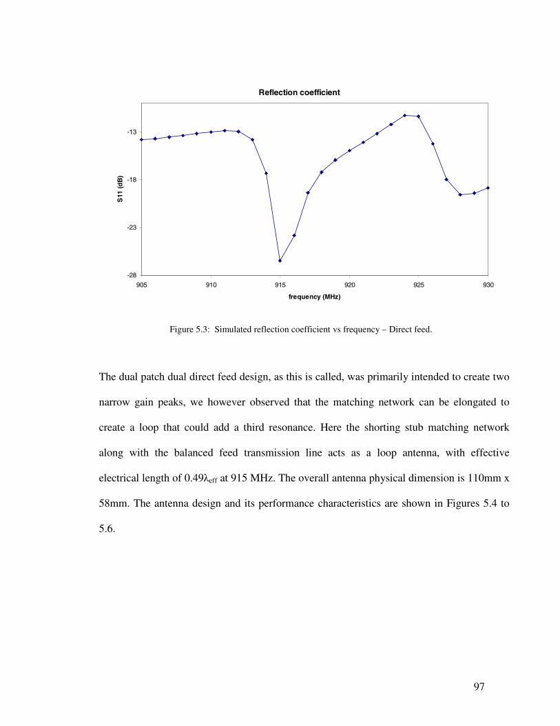
97
Reflection coefficient
-28
-23
-18
-13
905 910 915 920 925 930
frequency (MHz)
S11
(dB
)
Figure 5.3: Simulated reflection coefficient vs frequency – Direct feed.
The dual patch dual direct feed design, as this is called, was primarily intended to create two
narrow gain peaks, we however observed that the matching network can be elongated to
create a loop that could add a third resonance. Here the shorting stub matching network
along with the balanced feed transmission line acts as a loop antenna, with effective
electrical length of 0.49λeff at 915 MHz. The overall antenna physical dimension is 110mm x
58mm. The antenna design and its performance characteristics are shown in Figures 5.4 to
5.6.
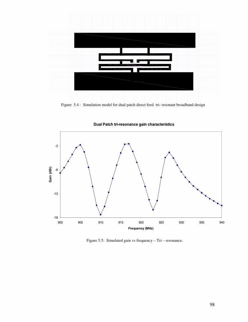
98
Port1
Figure 5.4 : Simulation model for dual patch direct feed tri- resonant broadband design
Dual Patch tri-resonance gain characteristics
-18
-13
-8
-3
900 905 910 915 920 925 930 935 940
Frequency (MHz)
Gai
n(d
Bi)
Figure 5.5: Simulated gain vs frequency – Tri – resonance.
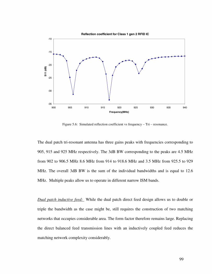
99
Reflection coefficient for Class 1 gen 2 RFID IC
-35
-30
-25
-20
-15
-10
900 905 910 915 920 925 930 935 940
Frequency(MHz)
S11
(dB
)
Figure 5.6: Simulated reflection coefficient vs frequency – Tri – resonance.
The dual patch tri-resonant antenna has three gains peaks with frequencies corresponding to
905, 915 and 925 MHz respectively. The 3dB BW corresponding to the peaks are 4.5 MHz
from 902 to 906.5 MHz 8.6 MHz from 914 to 918.6 MHz and 3.5 MHz from 925.5 to 929
MHz. The overall 3dB BW is the sum of the individual bandwidths and is equal to 12.6
MHz. Multiple peaks allow us to operate in different narrow ISM bands.
Dual patch inductive feed: While the dual patch direct feed design allows us to double or
triple the bandwidth as the case might be, still requires the construction of two matching
networks that occupies considerable area. The form factor therefore remains large. Replacing
the direct balanced feed transmission lines with an inductively coupled feed reduces the
matching network complexity considerably.
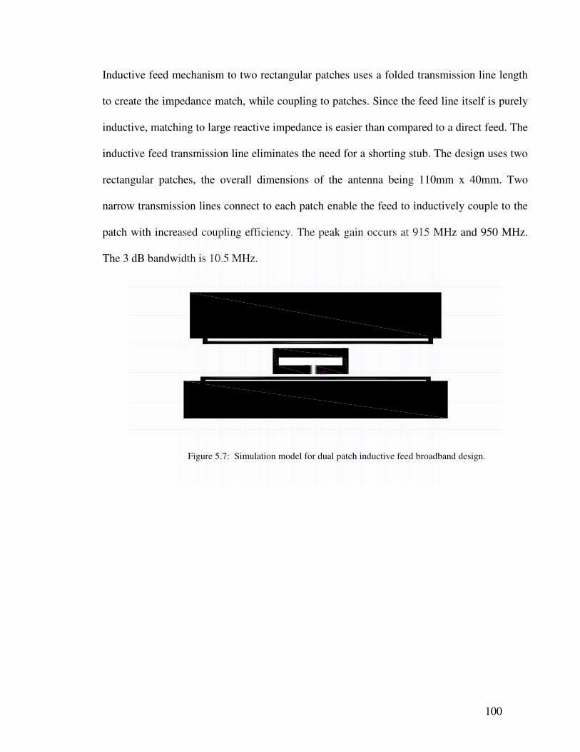
100
Inductive feed mechanism to two rectangular patches uses a folded transmission line length
to create the impedance match, while coupling to patches. Since the feed line itself is purely
inductive, matching to large reactive impedance is easier than compared to a direct feed. The
inductive feed transmission line eliminates the need for a shorting stub. The design uses two
rectangular patches, the overall dimensions of the antenna being 110mm x 40mm. Two
narrow transmission lines connect to each patch enable the feed to inductively couple to the
patch with increased coupling efficiency. The peak gain occurs at 915 MHz and 950 MHz.
The 3 dB bandwidth is 10.5 MHz.
Port1
Figure 5.7: Simulation model for dual patch inductive feed broadband design.
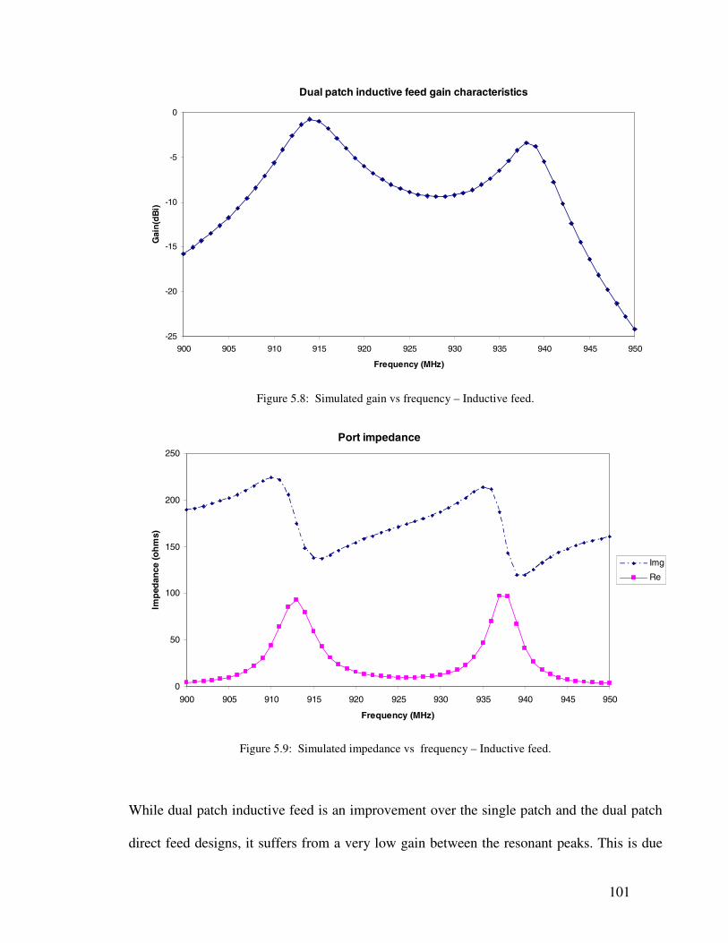
101
Dual patch inductive feed gain characteristics
-25
-20
-15
-10
-5
0
900 905 910 915 920 925 930 935 940 945 950
Frequency (MHz)
Gai
n(d
Bi)
Figure 5.8: Simulated gain vs frequency – Inductive feed.
Port impedance
0
50
100
150
200
250
900 905 910 915 920 925 930 935 940 945 950
Frequency (MHz)
Imp
edan
ce(o
hm
s)
Img
Re
Figure 5.9: Simulated impedance vs frequency – Inductive feed.
While dual patch inductive feed is an improvement over the single patch and the dual patch
direct feed designs, it suffers from a very low gain between the resonant peaks. This is due

102
the induced currents in the coupled patches flowing in opposite directions resulting in loss of
radiated power.
The above implementations are useful in operating over multiple narrow ISM frequencies,
like ETSI (865-868 MHz), Japan (953-956) etc. In operating over FCC, which has a
bandwidth of 28 MHz, from 902 to 930 MHz, these designs cover only one third of the
available bandwidth. With RFID readers frequency hoping over the entire bandwidth, tags
that have selective response regions (i.e. narrow peak gain followed by low gain regions)
such as the above could result in reduced number of reads at a fixed distance. Maintaining
an acceptable minimum gain over the entire bandwidth is necessary to overcome this
problem. The dual patch combined inductive and direct feed achieves this performance.
Dual patch combined feed: Combining the techniques of direct and inductive feed enables
us to critically couple to both the elements of the array without canceling the currents
severely. In this design one patch is connected to a pair of transmission lines that act as a
balanced feed. A short circuit stub is connected across the feed lines. The section of
balanced feed line below the shorting stub and the shorting stub itself form an inductive loop
that couples with the second patch. The effects of coupling and transmission line length on
resonant frequency are not well understood, the design therefore is manually tuned based on
simulations to achieve the right frequencies of resonance and impedance match. Figure 5.10
shows the simulation model and Figures 5.11 and 5.12 show the performance characteristics.
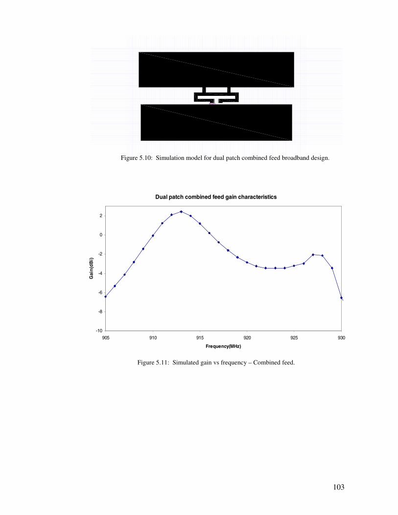
103
Port1
Figure 5.10: Simulation model for dual patch combined feed broadband design.
Dual patch combined feed gain characteristics
-10
-8
-6
-4
-2
0
2
905 910 915 920 925 930
Frequency(MHz)
Gai
n(d
Bi)
Figure 5.11: Simulated gain vs frequency – Combined feed.
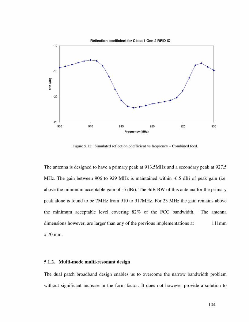
104
Reflection coefficient for Class 1 Gen 2 RFID IC
-25
-20
-15
-10
905 910 915 920 925 930
Frequency (MHz)
S11
(dB
)
Figure 5.12: Simulated reflection coefficient vs frequency – Combined feed.
The antenna is designed to have a primary peak at 913.5MHz and a secondary peak at 927.5
MHz. The gain between 906 to 929 MHz is maintained within -6.5 dBi of peak gain (i.e.
above the minimum acceptable gain of -5 dBi). The 3dB BW of this antenna for the primary
peak alone is found to be 7MHz from 910 to 917MHz. For 23 MHz the gain remains above
the minimum acceptable level covering 82% of the FCC bandwidth. The antenna
dimensions however, are larger than any of the previous implementations at 111mm
x 70 mm.
5.1.2. Multi-mode multi-resonant design
The dual patch broadband design enables us to overcome the narrow bandwidth problem
without significant increase in the form factor. It does not however provide a solution to

105
creating small metal mountable broadband RFID tags. Using meandered transmission lines
can effectively reduce the physical dimension of the antenna, the gain bandwidth of the
antenna will however be severely reduced as aperture is reduced. It is necessary at this point
to recall that we can extend the principle of balanced feed mechanism to all symmetric
microstrip patch geometries discussed in Section 2.4.1.
Microstrip patches geometries such as a square, circle, ring that have bilateral symmetry are
capable of multiple modes of operation as they can have more than one pair of radiating
edges depending on the electrical length and the current flow direction. Using these
geometries with slots to reduce the physical size, while generating multiple modes could
effectively combat both the bandwidth and the form factor problem associated with planar
microstrip RFID tags.
There is immense scope in exploring new designs that will use coupled feed mechanisms
with meandered patch geometries to further reduce matching network size and complexity.
There is a need to also thoroughly investigate the effects of planar balanced feed mechanism
on the microstrip patch, which will enable us to analytically determine the critical parameters
such as the feed line characteristics and matching network design to achieve optimum
performance under the constraints of low profile substrate, small form factor and cost
effective implementation. More rigorous test procedures need to be developed to test and
analyze the performance characteristics of these designs.

106
Chapter 6
Conclusions
The research motivation for this thesis was to show that a microstrip antenna can be
designed with dual feed transmission lines resulting in a balanced feed. The microstrip
antenna thus designed is completely planar in nature and does not have any cross-layered
structures. The theory for the design of a balanced feed microstrip antenna stems from the
traditional odd mode symmetry of the design analysis that allows us to simplify the balanced
feed design to the well understood, single microstripline feed. Odd mode analysis alone is
therefore sufficient to describe the working of the microstrip antenna with balanced feed
mechanism.
The primary application for this type of microstrip antenna is in the field of RFID
implementation where a cost effective solution to identify and track metal and high dielectric
materials was necessary. The planar microstrip antenna with balanced feed eliminates the
need for any cross–layered structures such as vias or shorting walls in the construction of a
microstrip RFID tag and thus reduces the manufacturing complexity and therefore the cost
associated with existing microstrip RFID solutions.
The balanced feed microstrip antenna was implemented using readily available materials that
were characterized in the lab by experimental methods. The design consisted of a an antenna
with shorting stub matching circuit to for impedance matching to the RFID IC on high
density polyethylene substrate and a ground plane. The effects of various design parameters

107
were first analyzed by extensive simulations, an initial set of values were selected based on
these studies as the starting point for the microstrip antenna design.
Initial design was single microstrip patch antenna with dual shorting stub matching network,
further experimentation showed that the similar results could be achieved with a single
shorting stub matching network, thus reducing form-factor and design complexity.
Optimization of the design is seen to involve numerous tradeoffs due to fact that the effects
design parameters are inter related and there is no specific optimization rule. The constraints
of low profile and small form-factor under which the antenna was designed limited the
extent to which antenna efficiency and bandwidth could be increased. The final design of the
microstrip antenna with balanced feed was made to operate in FCC RFID frequencies with
peak performance of -1.25dBi at 915 MHz. In order to validate the simulation results a
prototype was fabricated and its characteristics were experimentally measured using standard
lab equipment as well as with the application oriented RFID setup. Our measurements while
validating the simulation results to a larger extent showed better gain characteristics than
expected. We realize that there are certain inaccuracies and assumptions on which the
simulated and measure results are based that could result in this difference between
simulation and measurement.
A comparison with some of the existing UHF RFID tags has proved that our design is
capable of achieving consistent performance when attached to any material. Our prototype
tag had greater free space performance than any other tag, and maintained the performance
even when placed on metal sheets or containers with high dielectric substances like water.

108
The optimized microstrip antenna with balanced feed mechanism of UHF RFID proposed in
this thesis provides an attractive solution to the metal-water problem associated with passive
UHF RFID tags. The over all performance of the prototype was satisfactory and the design
goals were achieved, the concept of microstrip patch antenna with balanced feed mechanism
is therefore considered to be successfully implemented and tested. It however is not the
complete solution in itself as it suffers from narrow bandwidth, cannot be operated in ISM
bands worldwide, and, is not nearly as small in size as desired for certain applications.
We explored some broadband techniques that could be used to overcome the problems
associated with the current design. Dual patch with direct and coupled fed techniques were
designed and found to have more than twice the bandwidth that could be achieved with a
single patch design. It was also noted that development of mathematical models to predict
the effects of various parameter values on the antenna performance is necessary along with a
thorough procedures to test and validate the designs. The fact that industry needs are yet to
be fully addressed shows that further research initiatives are need in this direction.

109
References
[1] Kwon, H. and Lee B.: ‘Compact slotted planar inverted-F RFID tag mountable on
metallic objects.’ IEEE Electronics Letters, November 2005, Vol. 41, pp1308-1310.
[2] Ukkonen, L., Engels, D., Sydanheimo, L., and Kivikoski, M.: ‘Planar wire-type
inverted-F RFID tag antenna mountable on metallic objects.’ IEEE Int. Symp. on
AP-S, June 2004, Vol. 1, pp. 101–104.
[3] Choi, W., Son, H. W., Ji-Hoon Bae, Choi, Y. G., Cheol Sig Pyo and Jong Suk Chae:
‘An RFID tag using a planar Inverted F antenna capable of being stuck to metallic
objects.’ ETRI Journal, April 2006, Vol. 28, No. 2, pp 216-218.
[4] Carl Mueller, Introduction to RFID, March 2004,
http://www.corefunction.com/resources/wp/introduction_rfid.pdf
[5] FKI logistics, RFID for the Real World, 2005,
[6] Laran RFID, Basic introduction to RFID technology and its use in supply chains,
White paper , April 2004.
[7] Jim Eagleson, RFID: The Early Years, 1980 --- 1990,
http://members.surfbest.net/eaglesnest/rfidhist.htm
[8] Symbol Technology, Understanding the Key Issues in Radio Frequency
Identification (RFID), White paper, 2004.
[9] Logistics and material readiness, home page:
http://www.acq.osd.mil/log/rfid/index.htm, 2005.

110
[10] Wynne, M. W., Radio frequency identification (RFID) policy. Policy statement,
The Under Secretary of Defense, July 30 2004.
[11] Ann Marie Phaneuf, Meeting The EPC RFID Mandates: Where To Begin, Weber
Marketing Systems Inc., White paper
[12] Ahmed ElAmin, RFID advances help food traceability,
http://www.foodnavigator-usa.com/news/ng.asp?id=65062-idtechex-rfid-
traceability, 2006
[13] RFSAW, The Global SAW Tag – A New Technical Approach to RFID, White
paper, 2004
[14] Ramakrishnan K. N. M.: ‘Performance Benchmarks for Passive UHF RFID Tags.’
Masters Thesis report, 2005
[15] Finkenzeller K., RFID Handbook, Wiley & Sons, 2 edition, 2003.
[16] Definition of Inductive coupling,
http://en.wikipedia.org/wiki/Inductive_coupling , 2006.
[17] Sarma, S. and Engels, D. W., On the future of RFID tags and protocols, White
paper, Auto-ID Center, Massachusetts Institute of Technology, 2003.
[18] Powell K., Passive Radio Frequency Identification – A Primer for New RF
Regulations, Matrics, 2003.
[19] Balanis, C.A., Antenna Theory: Analysis and Design, John Wiley & Sons, Inc,
1997.

111
[20] Stutzman, W.L., and Thiele, G.A., Antenna Theory and Design, John Wiley &
Sons, Inc, 1998.
[21] Lo, Y. T., and Lee S. W., Antenna handbook: Antenna theory, Vol.2, International
Thompson Publishing, Inc, 1993.
[22] Glover, B., and Bhatt, H., RFID Essentials, O’Reilly Media, Inc, 2006
[23] Catherine, M.: ‘Symbol Announces Gen 2 Tags, Converter Program.’ RFID
Journal, News article, May 2006.
[24] Alien Technology – RFID tags,
http://www.alientechnology.com/products/rfid_tags.php
[25] Avery Dennison RFID: Products: Portfolio,
http://www.rfid.averydennison.com/us/products_portfolio.php
[26] Deschamps, G. A.: ‘Microstrip Microwave Antennas.’ The 3rd Symp. on The
USFA Antenna Research and Development Program, University of Illinois
Monticello, Illinois, October 1953.
[27] Hirvonen, M., Pursula, P., Jaakkola, K., and Laukkanen, K.: ‘Planar inverted-F
antenna for radio frequency identification.’ IEEE Electronic letters. 2004, Vol. 40,
pp. 848–850.
[28] Bhattacharyya, A. K., and Garg, R.: ‘Generalised transmission line model for
microstrip patches.’ IEE Proceedings, 1985, Vol. 132, pp. 93–98.
[29] Derneryd A.G.: ‘Linearly Polarized Microstrip Antennas.’ IEEE Trans. on AP,
November 1976, Vol. AP-24, pp. 846 – 851.

112
[30] Lo, Y. T., Solomon, D., and Richards W.F.: ‘Theory and Experiment on Microstrip
antennas.’ IEEE Trans. on AP, 1979, Vol. AP-27, pp. 137 – 149.
[31] Richards W.F., Lo, Y. T., and Harrison D. D.: ‘An Improved theory for Microstrip
antennas and Application.’ IEEE Trans. on AP, 1981, Vol. AP-29, pp. 38 – 46.
[32] Garg, R., Bhartia, P., Bahl, I., and Ittipiboon, A., Microstrip Antenna Design
Handbook, Artech House, Inc, 2001.
[33] Nakar, P. S.: ‘Design of a compact Microstrip Patch Antenna for use in
Wireless/Cellular Devices.’ Masters Thesis report, 2004.
[34] Kumar, G., and Ray, K.P., Broadband Microstrip Antennas, Artech House, Inc,
2003.
[35] Waterhouse, B. R., Microstrip Patch Antennas: A Designer’s Guide, Kluwer
Academic Publishers, 2003.
[36] Bancroft, R., Microstrip and Printed Antenna Design, Noble Publishing
Corporation, 2004.
[37] Definition of Inverted-F antenna,
www.qsl.net/kb7qhc/antenna/Inverted%20F/index.htm , 2006.
[38] Pozar, D. M., Microwave Engineering, Second Edition, John Wiley & Sons, Inc,
1988.
[39] ST Micro, XRA00 UHF EPCglobal Class 1b Contactless Memory Chip 96 bit ePC
with Inventory and Kill Function, Technical report, 2005.

113
[40] Imping RFID Technology Series, The RFID Antenna: Maximum Power Transfer,
Technical report, 2005.
[41] Definition of dielectric constant,
http://www.answers.com/topic/dielectric-constant , 2006
[42] Integrated publishing, Electrical Engineering Training series, Dielectric losses,
http://www.tpub.com/content/neets/14182/css/14182_116.htm , 2006
[43] Definition of Loss tangent,
http://www.rfcafe.com/references/electrical/dielectric_constants_strengths.htm ,
2006
[44] Gonzalo, R., P. de Maagt, and Sorolla, M.: ‘Enhanced Patch-Antenna Performance
by Suppressing Surface waves Using Photonic-Bandgap Substrates.’ IEEE Trans.
Microwave theory and techniques, 1999, Vol. MTT- 47, pp. 2131 – 2138.
[45] SAMSys Technologies, Inc, SAMSys MP9320 UHF Reader - Field Installation and
Calibration Guide, 2005.
[46] Newman, E.H. and Tylyathan, P., “Analysis of Microstrip Antennas Using Moment
Methods.” IEEE Trans. on AP., January 1981, Vol. AP-29, No. 1, pp. 47-53.
[47] Harrington. R.F., Field Computation by Moment Methods, Macmillan, New York,
1968.
114
Appendix - A
The frequency bands used in different countries for passive UHF RFID are as detailed in
Table A1.
Table A1: Frequency band of RFID operation in different countries
Country Frequency of operation
Federal Communications commission
(FCC) - USA and Canada902-928MHz
Korean frequency 910-914 MHz
Korean and Singapore frequency 923-925 MHz
Hong Kong frequency 920-925 MHz
European Telecommunications
Standards Institute (ETSI ) - Europe865-868MHz
Table A1: Frequency band of RFID operation in different countries
The SAMsys MP9320 v2.8 reader and circularly polarized UHF antenna was used in this
thesis for all tag – reader measurements. The reader uses a combination of TPC register and
the VFx registers [45] for frequency hopping in a particular frequency band. The FCC and
ETSI frequency hopping tables are given in Table A2 and Table A3 respectively
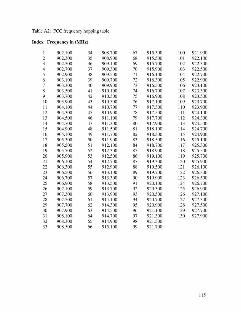
115
Table A2: FCC frequency hopping table
Index Frequency in (MHz)
1 902.1002 902.3003 902.5004 902.7005 902.9006 903.1007 903.3008 903.5009 903.70010 903.90011 904.10012 904.30013 904.50014 904.70015 904.90016 905.10017 905.30018 905.50019 905.70020 905.90021 906.10022 906.30023 906.50024 906.70025 906.90026 907.10027 907.30028 907.50029 907.70030 907.90031 908.10032 908.30033 908.500
34 908.70035 908.90036 909.10037 909.30038 909.50039 909.70040 909.90041 910.10042 910.30043 910.50044 910.70045 910.90046 911.10047 911.30048 911.50049 911.70050 911.90051 912.10052 912.30053 912.50054 912.70055 912.90056 913.10057 913.30058 913.50059 913.70060 913.90061 914.10062 914.30063 914.50064 914.70065 914.90066 915.100
67 915.30068 915.50069 915.70070 915.90071 916.10072 916.30073 916.50074 916.70075 916.90076 917.10077 917.30078 917.50079 917.70080 917.90081 918.10082 918.30083 918.50084 918.70085 918.90086 919.10087 919.30088 919.50089 919.70090 919.90091 920.10092 920.30093 920.50094 920.70095 920.90096 921.10097 921.30098 921.50099 921.700
100 921.900101 922.100102 922.300103 922.500104 922.700105 922.900106 923.100107 923.300108 923.500109 923.700110 923.900111 924.100112 924.300113 924.500114 924.700115 924.900116 925.100117 925.300118 925.500119 925.700120 925.900121 926.100122 926.300123 926.500124 926.700125 926.900126 927.100127 927.300128 927.500129 927.700130 927.900

116
Table A3: ETSI Frequency hopping table
Index Frequency (MHz)1 865.1002 865.3003 865.5004 865.7005 865.9006 866.1007 866.3008 866.5009 866.70010 866.90011 867.10012 867.30013 867.50014 867.70015 867.900