magnetism and molecular materials : investigating magnetic ... · cox, m. (2015). magnetism and...
TRANSCRIPT

Magnetism and molecular materials : investigating magneticfield effects in organic semiconductorsCitation for published version (APA):Cox, M. (2015). Magnetism and molecular materials : investigating magnetic field effects in organicsemiconductors. Eindhoven: Technische Universiteit Eindhoven.
Document status and date:Published: 01/01/2015
Document Version:Publisher’s PDF, also known as Version of Record (includes final page, issue and volume numbers)
Please check the document version of this publication:
• A submitted manuscript is the version of the article upon submission and before peer-review. There can beimportant differences between the submitted version and the official published version of record. Peopleinterested in the research are advised to contact the author for the final version of the publication, or visit theDOI to the publisher's website.• The final author version and the galley proof are versions of the publication after peer review.• The final published version features the final layout of the paper including the volume, issue and pagenumbers.Link to publication
General rightsCopyright and moral rights for the publications made accessible in the public portal are retained by the authors and/or other copyright ownersand it is a condition of accessing publications that users recognise and abide by the legal requirements associated with these rights.
• Users may download and print one copy of any publication from the public portal for the purpose of private study or research. • You may not further distribute the material or use it for any profit-making activity or commercial gain • You may freely distribute the URL identifying the publication in the public portal.
If the publication is distributed under the terms of Article 25fa of the Dutch Copyright Act, indicated by the “Taverne” license above, pleasefollow below link for the End User Agreement:www.tue.nl/taverne
Take down policyIf you believe that this document breaches copyright please contact us at:[email protected] details and we will investigate your claim.
Download date: 13. Jul. 2020

Matthijs Cox
and
Investigating magnetic field effects in organic semiconductors
Magnetism and Molecular MaterialsInvestigating magnetic field effects in organic semiconductors
PROEFSCHRIFT
ter verkrijging van de graad van doctor aan deTechnische Universiteit Eindhoven, op gezag van derector magnificus prof.dr.ir. C.J. van Duijn, vooreen commissie aangewezen door het College voor
Promoties, in het openbaar te verdedigen opdonderdag 11 februari 2015 om 16:00 uur
door
Matthijs Cox
geboren te Valkenswaard
Dit proefschrift is goedgekeurd door de promotoren en de samenstelling vande promotiecommissie is als volgt:
voorzitter: prof.dr.ir. G.M.W. Kroesen1e promotor: prof.dr. B. Koopmans2e promotor: prof.dr.ir. H.J.M. Swagtencopromotor: dr. S.C.J. Meskersleden: prof.dr. N. Greenham (University of Cambridge)
prof.dr. M. Wohlgenannt (University of Iowa)prof.dr.ir. W.G. van der Wiel (Universiteit Twente)dr. P.A. Bobbert

A catalogue is available from the Eindhoven University of Technology Library
Printed by Ipskamp Drukkers B.V., Enschede
Cover design by Matthijs Cox
The work described in this thesis has been carried out at the group Physics ofNanostructures at the Department of Applied Physics of the EindhovenUniversity of Technology
This research is supported by the Dutch Technology Foundation STW, whichis part of the Netherlands Organisation for Scientific Research (NWO) andpartly funded by the Ministry of Economic Affairs (project number 11424)
Contents
1 Introduction to organic spintronics 11.1 Organic electronics . . . . . . . . . . . . . . . . . . . . . . . 21.2 The role of spin . . . . . . . . . . . . . . . . . . . . . . . . . 61.3 Organic magnetoresistance . . . . . . . . . . . . . . . . . . . 101.4 Scope and outline of this thesis . . . . . . . . . . . . . . . . . 13
2 Modelling organic magnetoresistance 152.1 Microscopic mechanisms . . . . . . . . . . . . . . . . . . . . 162.2 Spin mixing calculations . . . . . . . . . . . . . . . . . . . . 202.3 Drift-diffusion model . . . . . . . . . . . . . . . . . . . . . . 232.4 Tuning the mechanisms in experiments . . . . . . . . . . . . 31
3 Traps and trions as origin of organic magnetoresistance 373.1 Introduction . . . . . . . . . . . . . . . . . . . . . . . . . . . 383.2 Experimental results . . . . . . . . . . . . . . . . . . . . . . 403.3 Trion model . . . . . . . . . . . . . . . . . . . . . . . . . . . 423.4 Analytical calculations . . . . . . . . . . . . . . . . . . . . . 453.5 Numerical calculations . . . . . . . . . . . . . . . . . . . . . 483.6 Discussion . . . . . . . . . . . . . . . . . . . . . . . . . . . . 503.7 Conclusion . . . . . . . . . . . . . . . . . . . . . . . . . . . 51
4 Investigating the influence of traps on organic magnetoresis-tance by molecular doping 534.1 Introduction . . . . . . . . . . . . . . . . . . . . . . . . . . . 544.2 Experimental results . . . . . . . . . . . . . . . . . . . . . . 564.3 Analysis . . . . . . . . . . . . . . . . . . . . . . . . . . . . . 604.4 Influence of oxygen . . . . . . . . . . . . . . . . . . . . . . . 644.5 Conclusion . . . . . . . . . . . . . . . . . . . . . . . . . . . 65
i
ii CONTENTS
5 Spectroscopic evidence for trap-dominated magnetic field effectsin organic semiconductors 675.1 Introduction . . . . . . . . . . . . . . . . . . . . . . . . . . . 685.2 Experimental results . . . . . . . . . . . . . . . . . . . . . . 695.3 Numerical calculations . . . . . . . . . . . . . . . . . . . . . 745.4 Implications and conclusion . . . . . . . . . . . . . . . . . . 80
6 Anisotropic magnetoconductance in polymer thin films 816.1 Introduction . . . . . . . . . . . . . . . . . . . . . . . . . . . 826.2 Experimental details . . . . . . . . . . . . . . . . . . . . . . 836.3 Low field anisotropy . . . . . . . . . . . . . . . . . . . . . . 836.4 High field anisotropy . . . . . . . . . . . . . . . . . . . . . . 886.5 Conclusion . . . . . . . . . . . . . . . . . . . . . . . . . . . 93
7 ∆B-mechanism for fringe-field organic magnetoresistance 957.1 Introduction . . . . . . . . . . . . . . . . . . . . . . . . . . . 967.2 ∆B-mechanism . . . . . . . . . . . . . . . . . . . . . . . . . 977.3 Fringe-field magnetoresistance . . . . . . . . . . . . . . . . . 1017.4 Fringe-field magnetoresistance calculations . . . . . . . . . . 1037.5 Conclusion . . . . . . . . . . . . . . . . . . . . . . . . . . . 106
8 Future research and applications of organic spintronics 1078.1 Introduction . . . . . . . . . . . . . . . . . . . . . . . . . . . 1088.2 Magnetic domain wall sensing . . . . . . . . . . . . . . . . . 1098.3 Spin detection with magneto-optical methods . . . . . . . . . 1108.4 Engineering organic magnetoresistance . . . . . . . . . . . . 114
Summary 117
Samenvatting 121
Curriculum vitae 125
List of publications 127
Acknowledgements / Dankwoord 129
Bibliography 131
1Introduction to organicspintronics
In the field of organic spintronics, the spin of the electron is investigated andexploited in organic materials. Interdisciplinary research is at the core of this field.Studying the role of spin in organic semiconductors requires knowledge of physics,chemistry and materials science. Additionally, many of the physical processesare also relevant for biology, where spin plays an important role as well, e.g. inphotosynthesis and avian navigation. Given the broad scope and possible futureapplications, the field of organic spintronics has grown in popularity during the lastyears. In this chapter we will highlight several of the topics in organic spintronicsthat are of interest for this thesis, starting with the field of organic electronics.
1
2 Chapter 1 : Introduction to organic spintronics
b c
6x pz
LUMO (*)
HOMO ()
a
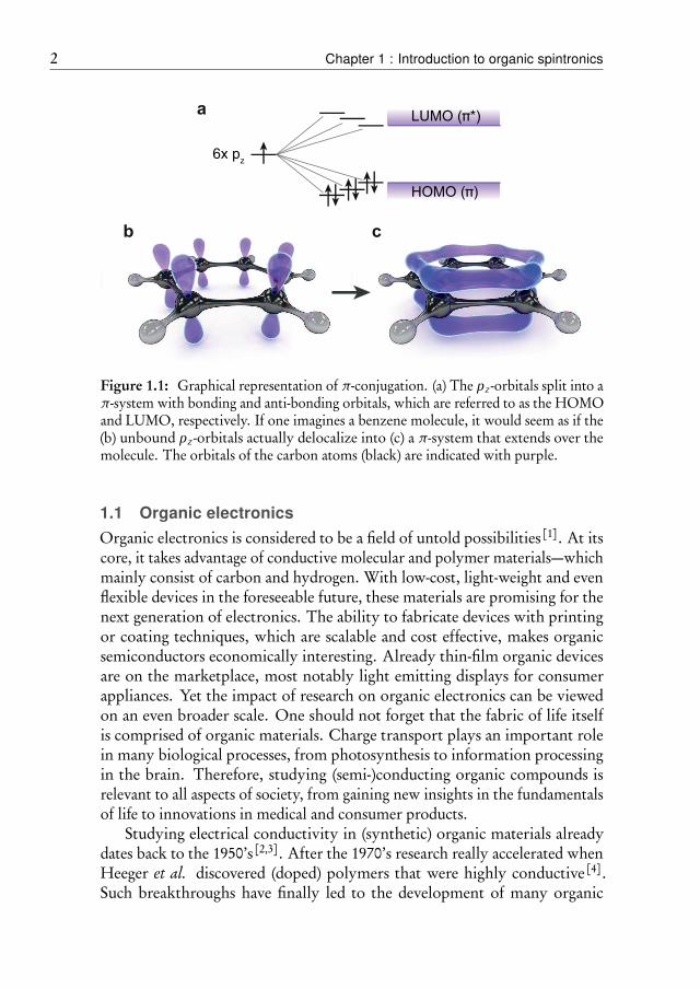
Figure 1.1: Graphical representation of π-conjugation. (a) The pz -orbitals split into aπ-system with bonding and anti-bonding orbitals, which are referred to as the HOMOand LUMO, respectively. If one imagines a benzene molecule, it would seem as if the(b) unbound pz -orbitals actually delocalize into (c) a π-system that extends over themolecule. The orbitals of the carbon atoms (black) are indicated with purple.
1.1 Organic electronics
Organic electronics is considered to be a field of untold possibilities[1]. At itscore, it takes advantage of conductive molecular and polymer materials—whichmainly consist of carbon and hydrogen. With low-cost, light-weight and evenflexible devices in the foreseeable future, these materials are promising for thenext generation of electronics. The ability to fabricate devices with printingor coating techniques, which are scalable and cost effective, makes organicsemiconductors economically interesting. Already thin-film organic devicesare on the marketplace, most notably light emitting displays for consumerappliances. Yet the impact of research on organic electronics can be viewedon an even broader scale. One should not forget that the fabric of life itselfis comprised of organic materials. Charge transport plays an important rolein many biological processes, from photosynthesis to information processingin the brain. Therefore, studying (semi-)conducting organic compounds isrelevant to all aspects of society, from gaining new insights in the fundamentalsof life to innovations in medical and consumer products.
Studying electrical conductivity in (synthetic) organic materials alreadydates back to the 1950’s[2,3]. After the 1970’s research really accelerated whenHeeger et al. discovered (doped) polymers that were highly conductive[4].Such breakthroughs have finally led to the development of many organic
1.1 Organic electronics 3
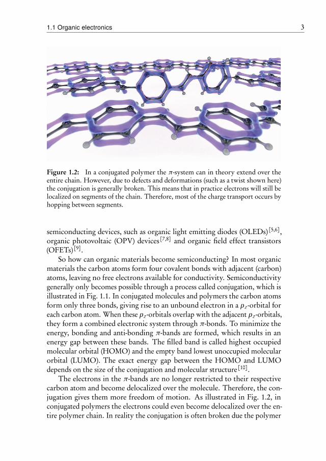
Figure 1.2: In a conjugated polymer the π-system can in theory extend over theentire chain. However, due to defects and deformations (such as a twist shown here)the conjugation is generally broken. This means that in practice electrons will still belocalized on segments of the chain. Therefore, most of the charge transport occurs byhopping between segments.
semiconducting devices, such as organic light emitting diodes (OLEDs)[5,6],organic photovoltaic (OPV) devices[7,8] and organic field effect transistors(OFETs)[9].
So how can organic materials become semiconducting? In most organicmaterials the carbon atoms form four covalent bonds with adjacent (carbon)atoms, leaving no free electrons available for conductivity. Semiconductivitygenerally only becomes possible through a process called conjugation, which isillustrated in Fig. 1.1. In conjugated molecules and polymers the carbon atomsform only three bonds, giving rise to an unbound electron in a pz -orbital foreach carbon atom. When these pz -orbitals overlap with the adjacent pz -orbitals,they form a combined electronic system through π-bonds. To minimize theenergy, bonding and anti-bonding π-bands are formed, which results in anenergy gap between these bands. The filled band is called highest occupiedmolecular orbital (HOMO) and the empty band lowest unoccupied molecularorbital (LUMO). The exact energy gap between the HOMO and LUMOdepends on the size of the conjugation and molecular structure[10].
The electrons in the π-bands are no longer restricted to their respectivecarbon atom and become delocalized over the molecule. Therefore, the con-jugation gives them more freedom of motion. As illustrated in Fig. 1.2, inconjugated polymers the electrons could even become delocalized over the en-tire polymer chain. In reality the conjugation is often broken due the polymer
4 Chapter 1 : Introduction to organic spintronics
a b
LUMO
HOMO
traps
E
DOS
Electric field
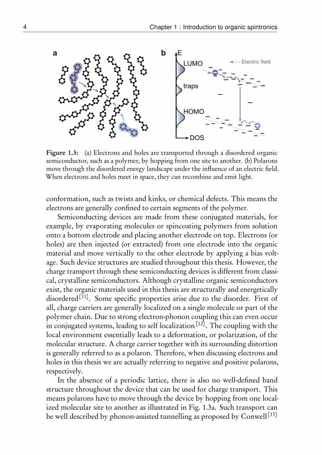
Figure 1.3: (a) Electrons and holes are transported through a disordered organicsemiconductor, such as a polymer, by hopping from one site to another. (b) Polaronsmove through the disordered energy landscape under the influence of an electric field.When electrons and holes meet in space, they can recombine and emit light.
conformation, such as twists and kinks, or chemical defects. This means theelectrons are generally confined to certain segments of the polymer.
Semiconducting devices are made from these conjugated materials, forexample, by evaporating molecules or spincoating polymers from solutiononto a bottom electrode and placing another electrode on top. Electrons (orholes) are then injected (or extracted) from one electrode into the organicmaterial and move vertically to the other electrode by applying a bias volt-age. Such device structures are studied throughout this thesis. However, thecharge transport through these semiconducting devices is different from classi-cal, crystalline semiconductors. Although crystalline organic semiconductorsexist, the organic materials used in this thesis are structurally and energeticallydisordered[11]. Some specific properties arise due to the disorder. First ofall, charge carriers are generally localized on a single molecule or part of thepolymer chain. Due to strong electron-phonon coupling this can even occurin conjugated systems, leading to self localization [12]. The coupling with thelocal environment essentially leads to a deformation, or polarization, of themolecular structure. A charge carrier together with its surrounding distortionis generally referred to as a polaron. Therefore, when discussing electrons andholes in this thesis we are actually referring to negative and positive polarons,respectively.
In the absence of a periodic lattice, there is also no well-defined bandstructure throughout the device that can be used for charge transport. Thismeans polarons have to move through the device by hopping from one local-ized molecular site to another as illustrated in Fig. 1.3a. Such transport canbe well described by phonon-assisted tunnelling as proposed by Conwell[13]
1.1 Organic electronics 5
and Mott[14] for disordered inorganic semiconductors. When a polaron hopsthrough the disordered energy landscape as shown in Fig. 1.3b, generally de-scribed by a Gaussian in organic semiconductors [15], it has to move up anddown in energy. This can be done by absorbing or emitting phonons. Millerand Abrahams[16] described the probability at which each hop occurs, showingit depends on the difference in distance and energy between each hoppingsite. The actual velocity with which the polarons move through a device isgenerally characterized by the mobility, which is the ability to move underthe influence of an electric field. This mobility depends on the electric field,the charge density and the temperature [17]. Finally, we note that due to thehopping transport in organic semiconductors, the mobility tends to be lowerthan in most inorganic semiconductors.
When electrons and holes are injected into an organic semiconductor thesecan find each other in space to form excitons and recombine. The definitionof an exciton in an organic semiconductor is a coupled electron-hole pairwith strong wavefunction overlap, which generally implies the electron andhole are on the same molecular site. Exciton decay can occur radiatively,which means a photon is emitted, or non-radiatively. The wavelength ofthe emitted light depends on the energy gap of the organic semiconductor,i.e. the difference between the HOMO and LUMO, and the exciton bindingenergy. The recombination process is typically described with the Langevinrecombination rate[18]. This is an effective rate that depends on the product ofthe electron and hole density (it is a bimolecular process), but also on the chanceof electrons and holes to find each other. Deviation from the Langevin formuladue to disorder should be small[19] and experiments confirm the manifestationof Langevin recombination[20]. The conversion of electrical power into lightvia polaron recombination is the working principle of the OLED, which is anapplication that has made organic semiconductors immensely popular.
Figure 1.3b also shows energetic states which may exist within the forbiddenenergy gap. These are very localized states, where polarons are trapped dueto their low energy. These states are, therefore, often referred to as traps andcan severely limit the charge transport. Polaron traps have been observed inmany organic semiconductors[21–23] and they can be described with a Gaussianenergy distribution just like the HOMO and LUMO [24]. The origin of thetraps is not entirely clear. It has been attributed to intrinsic defects (suchas polymer kinks)[25], to impurities left over from the synthesis and/or toenvironmental contamination[26]. Additionally, device degradation seems tocreate more traps[27].
Previously, we discussed bimolecular recombination of electrons and holes.Recombination is also possible when either of the polarons is trapped. It turnsout that such trap-assisted recombination can be described with Shockley-Read-
6 Chapter 1 : Introduction to organic spintronics
Hall recombination [28], which resembles a Langevin recombination processwhere one charge is assumed to have no mobility. The recombination on theinitial traps is often non-radiative and in that case traps are detrimental for lightemission. On the other hand, luminescent dyes, which can be inserted into anorganic device, also act as traps, yet allow one to tune the wavelength of theemitted light[29].
To briefly summarize, we have discussed how negative and positive chargesin the form of electron and hole polarons can be transported through organicsemiconductors and recombine to emit light. In the next section, we will moveon to the role spin plays in the charge transport and other properties of organicsemiconductors.
1.2 The role of spin
Where electronics makes full use of the charge of electrons to transport or storeinformation, the field of spintronics also exploits the spin degree of freedomof electrons[30,31]. Spin is an intrinsic property of particles and is stronglyrelated to magnetism, because it creates a magnetic dipole moment. A myriadof applications have been conceived for spintronics, most notably the so-calledmagnetoresistive sensors. Such sensors are used to read out the magneticinformation on hard disks, but they can be found in many other industrial,automotive, avionic and consumer applications. Spintronics is an ongoing andpromising field of research, with innovative technologies just around the corner.Novel approaches such as the magnetic racetrack memory[32] or magneticrandom access memory[33] might easily find their way into future data storageapplications.
Thus the spin degree of freedom of electrons seems to be utilized to itsfullest in inorganic spintronic devices. However, organic materials are stilllagging behind. This limits the use of organic materials in conjunction withmany conventional memory and sensing applications. Nevertheless, longspin lifetimes have been observed in organic materials, which is relevant fordevices that utilize the spin in storing and transporting information [34–38].Therefore, organic semiconductors are a promising candidate for spintronicapplications. The desire to understand and utilize spin-dependent processes inorganic semiconductors has led to the emergence of the research field calledorganic spintronics.
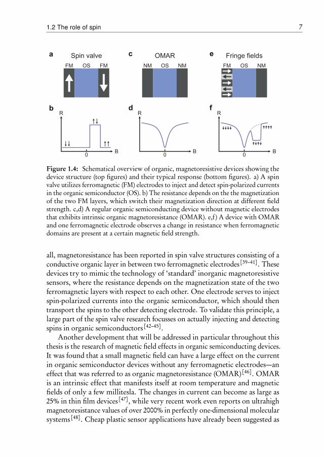
During the past decade, the young field of organic spintronics has beencatching up with its inorganic counterpart. In this field, different routes areinvestigated to study the role of spin in organic semiconductors and eventuallyrealize applications, such as inexpensive magnetic field sensors. An overviewof several possible organic magnetic field sensors is shown in Fig. 1.4. First of
1.2 The role of spin 7
FM OS FM NM OS NM FM OS NM
a c e
b d fR
0
R
0B
R
0
Spin valve OMAR Fringe fields
BB
Figure 1.4: Schematical overview of organic, magnetoresistive devices showing thedevice structure (top figures) and their typical response (bottom figures). a) A spinvalve utilizes ferromagnetic (FM) electrodes to inject and detect spin-polarized currentsin the organic semiconductor (OS). b) The resistance depends on the the magnetizationof the two FM layers, which switch their magnetization direction at different fieldstrength. c,d) A regular organic semiconducting device without magnetic electrodesthat exhibits intrinsic organic magnetoresistance (OMAR). e,f) A device with OMARand one ferromagnetic electrode observes a change in resistance when ferromagneticdomains are present at a certain magnetic field strength.
all, magnetoresistance has been reported in spin valve structures consisting of aconductive organic layer in between two ferromagnetic electrodes [39–41]. Thesedevices try to mimic the technology of ‘standard’ inorganic magnetoresistivesensors, where the resistance depends on the magnetization state of the twoferromagnetic layers with respect to each other. One electrode serves to injectspin-polarized currents into the organic semiconductor, which should thentransport the spins to the other detecting electrode. To validate this principle, alarge part of the spin valve research focusses on actually injecting and detectingspins in organic semiconductors[42–45].
Another development that will be addressed in particular throughout thisthesis is the research of magnetic field effects in organic semiconducting devices.It was found that a small magnetic field can have a large effect on the currentin organic semiconductor devices without any ferromagnetic electrodes—aneffect that was referred to as organic magnetoresistance (OMAR)[46]. OMARis an intrinsic effect that manifests itself at room temperature and magneticfields of only a few millitesla. The changes in current can become as large as25% in thin film devices[47], while very recent work even reports on ultrahighmagnetoresistance values of over 2000% in perfectly one-dimensional molecularsystems[48]. Cheap plastic sensor applications have already been suggested as
8 Chapter 1 : Introduction to organic spintronics
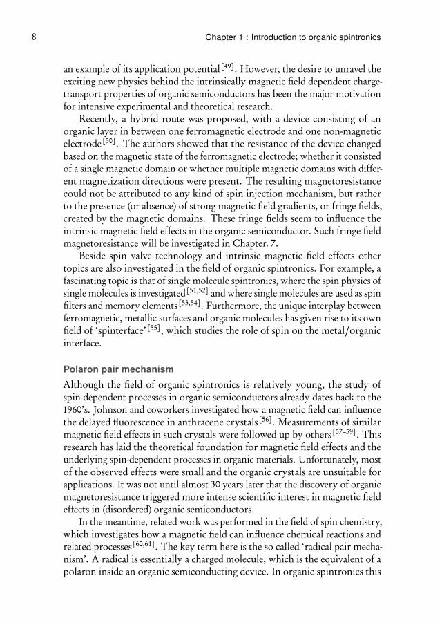
an example of its application potential [49]. However, the desire to unravel theexciting new physics behind the intrinsically magnetic field dependent charge-transport properties of organic semiconductors has been the major motivationfor intensive experimental and theoretical research.
Recently, a hybrid route was proposed, with a device consisting of anorganic layer in between one ferromagnetic electrode and one non-magneticelectrode [50]. The authors showed that the resistance of the device changedbased on the magnetic state of the ferromagnetic electrode; whether it consistedof a single magnetic domain or whether multiple magnetic domains with differ-ent magnetization directions were present. The resulting magnetoresistancecould not be attributed to any kind of spin injection mechanism, but ratherto the presence (or absence) of strong magnetic field gradients, or fringe fields,created by the magnetic domains. These fringe fields seem to influence theintrinsic magnetic field effects in the organic semiconductor. Such fringe fieldmagnetoresistance will be investigated in Chapter. 7.
Beside spin valve technology and intrinsic magnetic field effects othertopics are also investigated in the field of organic spintronics. For example, afascinating topic is that of single molecule spintronics, where the spin physics ofsingle molecules is investigated[51,52] and where single molecules are used as spinfilters and memory elements [53,54]. Furthermore, the unique interplay betweenferromagnetic, metallic surfaces and organic molecules has given rise to its ownfield of ‘spinterface’[55], which studies the role of spin on the metal/organicinterface.
Polaron pair mechanism
Although the field of organic spintronics is relatively young, the study ofspin-dependent processes in organic semiconductors already dates back to the1960’s. Johnson and coworkers investigated how a magnetic field can influencethe delayed fluorescence in anthracene crystals[56]. Measurements of similarmagnetic field effects in such crystals were followed up by others[57–59]. Thisresearch has laid the theoretical foundation for magnetic field effects and theunderlying spin-dependent processes in organic materials. Unfortunately, mostof the observed effects were small and the organic crystals are unsuitable forapplications. It was not until almost 30 years later that the discovery of organicmagnetoresistance triggered more intense scientific interest in magnetic fieldeffects in (disordered) organic semiconductors.
In the meantime, related work was performed in the field of spin chemistry,which investigates how a magnetic field can influence chemical reactions andrelated processes [60,61]. The key term here is the so called ‘radical pair mecha-nism’. A radical is essentially a charged molecule, which is the equivalent of apolaron inside an organic semiconducting device. In organic spintronics this
1.2 The role of spin 9
a b singlet triplet
kS kT
singlet
product
triplet
product
Beff
Bhf
B
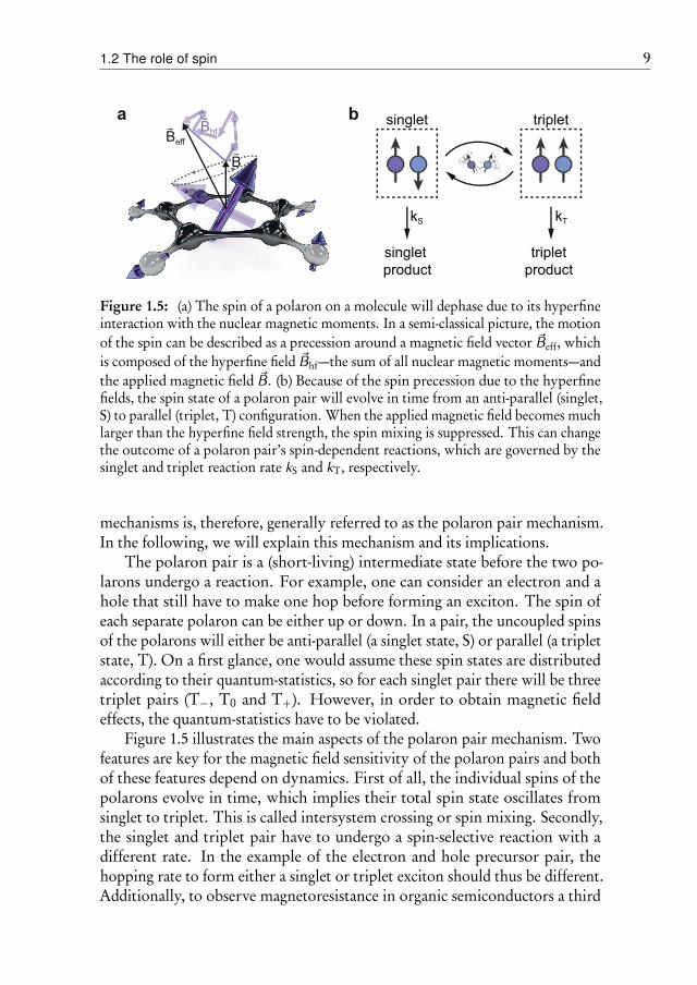
Figure 1.5: (a) The spin of a polaron on a molecule will dephase due to its hyperfineinteraction with the nuclear magnetic moments. In a semi-classical picture, the motionof the spin can be described as a precession around a magnetic field vector ~Beff, whichis composed of the hyperfine field ~Bhf—the sum of all nuclear magnetic moments—andthe applied magnetic field ~B. (b) Because of the spin precession due to the hyperfinefields, the spin state of a polaron pair will evolve in time from an anti-parallel (singlet,S) to parallel (triplet, T) configuration. When the applied magnetic field becomes muchlarger than the hyperfine field strength, the spin mixing is suppressed. This can changethe outcome of a polaron pair’s spin-dependent reactions, which are governed by thesinglet and triplet reaction rate kS and kT, respectively.
mechanisms is, therefore, generally referred to as the polaron pair mechanism.In the following, we will explain this mechanism and its implications.
The polaron pair is a (short-living) intermediate state before the two po-larons undergo a reaction. For example, one can consider an electron and ahole that still have to make one hop before forming an exciton. The spin ofeach separate polaron can be either up or down. In a pair, the uncoupled spinsof the polarons will either be anti-parallel (a singlet state, S) or parallel (a tripletstate, T). On a first glance, one would assume these spin states are distributedaccording to their quantum-statistics, so for each singlet pair there will be threetriplet pairs (T−, T0 and T+). However, in order to obtain magnetic fieldeffects, the quantum-statistics have to be violated.
Figure 1.5 illustrates the main aspects of the polaron pair mechanism. Twofeatures are key for the magnetic field sensitivity of the polaron pairs and bothof these features depend on dynamics. First of all, the individual spins of thepolarons evolve in time, which implies their total spin state oscillates fromsinglet to triplet. This is called intersystem crossing or spin mixing. Secondly,the singlet and triplet pair have to undergo a spin-selective reaction with adifferent rate. In the example of the electron and hole precursor pair, thehopping rate to form either a singlet or triplet exciton should thus be different.Additionally, to observe magnetoresistance in organic semiconductors a third
10 Chapter 1 : Introduction to organic spintronics
feature is required; the spin-selective reactions also need to influence the polarontransport. We will explain this last feature in more detail in the next chapter.
The first feature, spin mixing, arises due to the hyperfine interaction ofa polaron spin with the nuclear magnetic moments present in the organicmaterial, for example from hydrogen or nitrogen. A delocalized polaron willfeel many of these magnetic moments, which are all randomly oriented. Thesum of all these hyperfine interactions is often treated in a semi-classical wayas an effective magnetic field called the hyperfine field [62]. The distribution ofhyperfine fields can be described with a Gaussian function, where the standarddeviation is given by the hyperfine field strength. This hyperfine field strengthis generally on the order of a millitesla in organic semiconductors[37,63,64].
A spin that feels a magnetic field will precess around this magnetic field.Because the two spins in a polaron pair each feel a different hyperfine field,they will precess around a different axis and with a different speed. This meansthe total spin state oscillates from parallel to anti-parallel, so from singlet totriplet. The outcome of polaron reactions becomes dependent on this mixinginstead of on the spin statistics. When an external magnetic field is appliedthat is much larger than the hyperfine fields, all the polaron spins experience(approximately) the same effective field and the spin mixing is suppressed. Wenote that dephasing still occurs, so mixing from S to T0 is not suppressed ina magnetic field. The suppression of the spin mixing influences the polaronreaction outcome. Therefore, a magnetic field can influence polaron reactions.Other type of reactions exist that can be influenced with magnetic fields, suchas exciton-polaron reactions or exciton-exciton reactions. Although these donot classify as polaron pair mechanisms, the basic principles are much the same.
The radical (or polaron) pair mechanism is nowadays used to explain anabundance of different magnetic field effects. For example, the magnetic fielddependence of photosynthetic reactions has been reported and analyzed in theframework of radical pair models[65,66]. Another interesting example is that ofavian magnetoreception, where molecular reactions occurring in specializedproteins in a bird’s eye are suggested to be sensitive to the Earth’s magnetic fieldand it direction[67–69]. In the remainder of this thesis, we will use the polaronpair mechanism to explain magnetic field effects in organic semiconductordevices.
1.3 Organic magnetoresistance
Research of magnetic field effects in organic semiconductor devices began in1992 when Frankevich et al. observed magnetic field sensitive photoconduc-tivity in poly(phenylene vinylenes) (PPV) films[70]. In 2003 Kalinowski andcoworkers investigated intrinsic magnetoresistance in electroluminescent PPV-based films [71]. They showed that the current (or resistance) through such a
1.3 Organic magnetoresistance 11
device could change significantly. In their paper, the authors proposed that spinmixing in polaron pairs due to hyperfine fields is responsible. This research wasfollowed up by researchers from the University of Iowa[46,72], who called theeffect organic magnetoresistance (OMAR). The authors showed that organicmagnetoresistance is a bulk effect and can be observed in many different organiccompounds. With a background in inorganic spintronics, these researchers no-ticed that theories proposed for magnetoresistance in inorganic materials, suchas Lorentz-force deflection, hopping magnetoresistance or weak localizationwere unable to explain this low field, room-temperature effect in disordered,organic semiconductors. Similar to Kalinowski et al. they concluded that apolaron pair mechanism was the most suitable explanation.
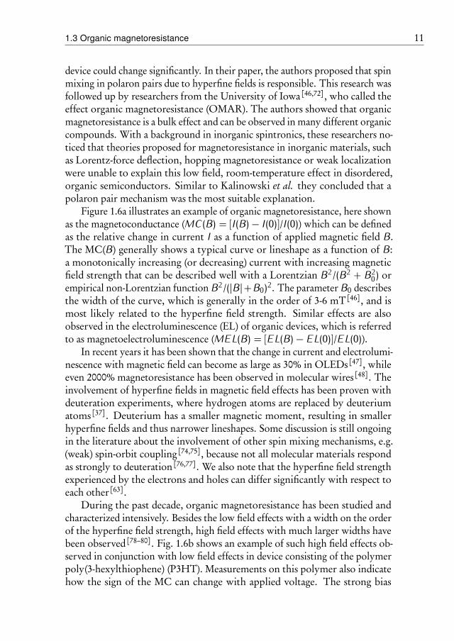
Figure 1.6a illustrates an example of organic magnetoresistance, here shownas the magnetoconductance (MC (B) = [I(B)− I(0)]/I(0)) which can be definedas the relative change in current I as a function of applied magnetic field B.The MC(B) generally shows a typical curve or lineshape as a function of B:a monotonically increasing (or decreasing) current with increasing magneticfield strength that can be described well with a Lorentzian B2/(B2 + B20) orempirical non-Lorentzian function B2/(|B|+B0)2. The parameter B0 describesthe width of the curve, which is generally in the order of 3-6 mT[46], and ismost likely related to the hyperfine field strength. Similar effects are alsoobserved in the electroluminescence (EL) of organic devices, which is referredto as magnetoelectroluminescence (MEL(B) = [EL(B)− EL(0)]/EL(0)).
In recent years it has been shown that the change in current and electrolumi-nescence with magnetic field can become as large as 30% in OLEDs[47], whileeven 2000% magnetoresistance has been observed in molecular wires[48]. Theinvolvement of hyperfine fields in magnetic field effects has been proven withdeuteration experiments, where hydrogen atoms are replaced by deuteriumatoms [37]. Deuterium has a smaller magnetic moment, resulting in smallerhyperfine fields and thus narrower lineshapes. Some discussion is still ongoingin the literature about the involvement of other spin mixing mechanisms, e.g.(weak) spin-orbit coupling[74,75], because not all molecular materials respondas strongly to deuteration[76,77]. We also note that the hyperfine field strengthexperienced by the electrons and holes can differ significantly with respect toeach other[63].
During the past decade, organic magnetoresistance has been studied andcharacterized intensively. Besides the low field effects with a width on the orderof the hyperfine field strength, high field effects with much larger widths havebeen observed [78–80]. Fig. 1.6b shows an example of such high field effects ob-served in conjunction with low field effects in device consisting of the polymerpoly(3-hexylthiophene) (P3HT). Measurements on this polymer also indicatehow the sign of the MC can change with applied voltage. The strong bias
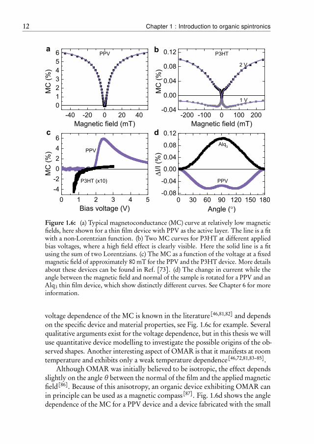
12 Chapter 1 : Introduction to organic spintronics
-40 -20 0 20 400123456
-200 -100 0 100 200-0.04
0.00
0.04
0.08
0.12
0 1 2 3 4 5-4-20246
0 30 60 90 120 150 180-0.08
-0.04
0.00
0.04
0.08
0.12
PPVM
C (%
)
Magnetic field (mT)
a b P3HT
2 V
1 V
MC
(%)
Magnetic field (mT)c
P3HT (x10)
PPV
MC
(%)
Bias voltage (V)
dAlq3
I/I (%
)
Angle ( )
PPV
Figure 1.6: (a) Typical magnetoconductance (MC) curve at relatively low magneticfields, here shown for a thin film device with PPV as the active layer. The line is a fitwith a non-Lorentzian function. (b) Two MC curves for P3HT at different appliedbias voltages, where a high field effect is clearly visible. Here the solid line is a fitusing the sum of two Lorentzians. (c) The MC as a function of the voltage at a fixedmagnetic field of approximately 80 mT for the PPV and the P3HT device. More detailsabout these devices can be found in Ref. [73]. (d) The change in current while theangle between the magnetic field and normal of the sample is rotated for a PPV and anAlq3 thin film device, which show distinctly different curves. See Chapter 6 for moreinformation.
voltage dependence of the MC is known in the literature [46,81,82] and dependson the specific device and material properties, see Fig. 1.6c for example. Severalqualitative arguments exist for the voltage dependence, but in this thesis we willuse quantitative device modelling to investigate the possible origins of the ob-served shapes. Another interesting aspect of OMAR is that it manifests at roomtemperature and exhibits only a weak temperature dependence[46,72,81,83–85].
Although OMAR was initially believed to be isotropic, the effect dependsslightly on the angle θ between the normal of the film and the applied magneticfield[86]. Because of this anisotropy, an organic device exhibiting OMAR canin principle can be used as a magnetic compass[87]. Fig. 1.6d shows the angledependence of the MC for a PPV device and a device fabricated with the small
1.4 Scope and outline of this thesis 13
molecule tris(8-hydroxyquinolinato)aluminium (Alq3). In Chapter 6 we try toshed more light on the origin of this anisotropy.
1.4 Scope and outline of this thesis
So far this chapter described the basic principles of organic semiconductorsand the role spin plays in these materials, with a strong emphasis on magneticfield effects. The research and knowledge of magnetic field effects in organicsemiconductors has grown tremendously in recent years. However, many openquestions still exist. Two major issues especially block a solid fundamentalunderstanding of magnetic field effects. On the microscopic level, the polaronpair mechanism explains how a magnetic field can influence reactions betweenexcitations. However, it is not known which spin-dependent excitations andreactions underlie the large magnetoresistance. On a more macroscopic level,the influence of polaron transport and device architecture on the magnetic fieldeffects remains unknown. It is also not well understood how magnetic fielddependent changes in polaron reactions translate into the observed magnetore-sistance. Especially, the role of traps on the magnetic field effects requires moreattention. Addressing the interplay between microscopic and macroscopicprocesses is essential in order to engineer and systematically improve organicspintronic devices.
In the next chapter, we fundamentally investigate the possible spin-dependentreactions at the origin of organic magnetoresistance (OMAR). We outline theproposed mechanisms and how to model them microscopically. To investigatethe influence of device physics on these mechanisms and OMAR, an elaboratenumerical (finite element) device model is used where the different mechanismsare integrated in the form of material parameters and particle densities. Thechapter ends with a controlled material system where the experimental resultsare explained with our complete modelling framework.
The experimental results of organic light emitting devices exhibit largemagnetoresistance (up to 20%) and remains most elusive to describe with ourframework. Some experiments in the literature indicate that traps play a role.Chapter 3, 4 and 5 deal with the inclusion of traps in the models and withexperimental methods to investigate the exact influence of traps with specializeddopants and chemically engineered polymers.
Chapter 6 describes another interesting property of organic magnetoresis-tance, the dependence on the orientation of the magnetic field. We providecompelling evidence that dipolar coupling between electron spins is at theorigin of this orientation dependence at small magnetic fields. However, newlyfound high field anisotropies remain somewhat of a mystery.
Chapter 7 investigates the influence of magnetic field gradients emanatingfrom magnetic domains on the magnetoresistance. We find that the fringe field

14 Chapter 1 : Introduction to organic spintronics
magnetoresistance is inversely proportional to square over the distance fromthe magnetic layer, which correlates to how the gradient of the magnetic fieldreduces with distance.
Organic semiconductors are an alluring class of materials and provide aunique platform to exploit the spin of the electron. In chapter 8, we discusspossible applications and future research in the field of organic spintronics.
2Modelling organicmagnetoresistance
In order to explain the surprisingly large, low field organic magnetoresistance(OMAR), several microscopic mechanisms have been proposed. These mechanismsdeal with interactions between spin-carrying particles. In this chapter we showhow such two particle interactions are modelled using a numerical density matrixformalism. However, the effect of such interactions on the polaron transportthrough a realistic device is relatively unknown. Therefore, we use finite element,drift-diffusion device models to determine the effect of device physics on thesemechanisms. The local magnetic field dependent reactions can be implemented viaa magnetic field dependent recombination, mobility and triplet formation rate. Anovel approach is used where we keep track of the subsequent particles formed ateach position within the device from these reactions, including excitons and trions.We find that the three mechanisms display clear fingerprints, with distinguishablecharacteristics such as sign, field scale and voltage dependence. We are able to usethis knowledge to identify the different mechanisms in a blend of materials, wherethe spin-based particle reactions are tuned.
Parts of this chapter are published as: M. Cox et al., Synth. Met. 173, 10 (2013)and P. Janssen, M. Cox et al., Nat. Commun. 4, 2286 (2013)
15
16 Chapter 2 : Modelling organic magnetoresistance
2.1 Microscopic mechanisms
Several mechanisms have been proposed for organic magnetoresistance. Theseare all based on the suppression of spin mixing of particle pairs prior to areaction, such as described in the previous chapter. The difference lies in whichparticles are used and how their subsequent reaction influences the current.First of all, interactions between equally charged polarons can be considered,so between two electrons or two holes [88]. Secondly, interactions betweenelectrons and holes can be considered [89]. The magnetic field effect can thenarise either through a change in their effective recombination rate[90] or vialong living triplet excitons that influence the charge transport[91,92].
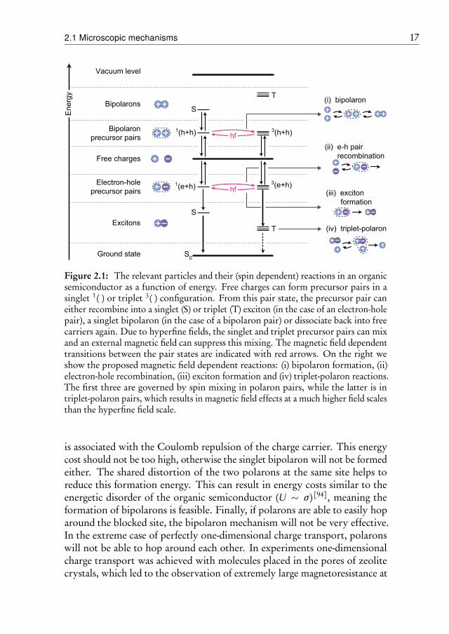
The mechanisms above have been used succesfully to describe low fieldeffects on the scale of the hyperfine field strength. Additionally, magneticfield effects have been observed on scales much larger than the hyperfine fieldstrength. At the end of this section, high field effects will be discussed withinthe framework of spin-selective reactions between triplet excitons and otherparticles, as well as due to differences in polaron g-factor. Fig. 2.1 gives anoverview of the relevant particle reactions for all the mechanisms in the formof an energy diagram.
Bipolaron mechanism
The first mechanism we discuss takes reactions between polarons with thesame charge as the underlying physics of the magnetic field effects [88]. Thisso-called bipolaron mechanism describes two polarons, where one is consideredstationary. The latter generally happens because the polaron occupies a lowenergetic site. The other polaron will have to pass the immobile polaron tocontribute to the current. To do this, both polarons have to temporarily occupythe same site. This doubly occupied site is referred to as a bipolaron. Such abipolaron will only be formed in the singlet state, because the triplet state ismuch higher in energy due to strong on-site exchange interactions[93]. So therate to form a triplet bipolaron is negligible, which means polaron pairs with atriplet spin state cannot pass each other. This concept is generally referred to asspin blocking. However, polaron pairs with a triplet spin state can evolve into asinglet state due to spin mixing, thus bypassing the spin blocking. As describedin the previous chapter, when a magnetic field is applied the spin mixing issuppressed. This means spin blocking becomes more effective in a magneticfield, resulting in less charge transport and thus a negative magnetoconductance.
The bipolaron mechanism depends strongly on several factors. Preferably,the trapped polaron is completely stationary and cannot escape its site. If it ismobile, the influence of bipolarons on the total charge transport diminishes.Secondly, the formation of a singlet bipolaron still has an energy cost U , which
2.1 Microscopic mechanisms 17
1(e+h)
1(h+h) 3(h+h)
3(e+h)
T
T
S
S
S0
hf
En
erg
y
hf
(i) bipolaron
Vacuum level
Ground state
Bipolarons
Free charges
Excitons
Bipolaron
precursor pairs
Electron-hole
precursor pairs
(ii) e-h pair
recombination
(iii) exciton
formation
(iv) triplet-polaron
Figure 2.1: The relevant particles and their (spin dependent) reactions in an organicsemiconductor as a function of energy. Free charges can form precursor pairs in asinglet 1( ) or triplet 3( ) configuration. From this pair state, the precursor pair caneither recombine into a singlet (S) or triplet (T) exciton (in the case of an electron-holepair), a singlet bipolaron (in the case of a bipolaron pair) or dissociate back into freecarriers again. Due to hyperfine fields, the singlet and triplet precursor pairs can mixand an external magnetic field can suppress this mixing. The magnetic field dependenttransitions between the pair states are indicated with red arrows. On the right weshow the proposed magnetic field dependent reactions: (i) bipolaron formation, (ii)electron-hole recombination, (iii) exciton formation and (iv) triplet-polaron reactions.The first three are governed by spin mixing in polaron pairs, while the latter is intriplet-polaron pairs, which results in magnetic field effects at a much higher field scalesthan the hyperfine field scale.
is associated with the Coulomb repulsion of the charge carrier. This energycost should not be too high, otherwise the singlet bipolaron will not be formedeither. The shared distortion of the two polarons at the same site helps toreduce this formation energy. This can result in energy costs similar to theenergetic disorder of the organic semiconductor (U ∼ σ )[94], meaning theformation of bipolarons is feasible. Finally, if polarons are able to easily hoparound the blocked site, the bipolaron mechanism will not be very effective.In the extreme case of perfectly one-dimensional charge transport, polaronswill not be able to hop around each other. In experiments one-dimensionalcharge transport was achieved with molecules placed in the pores of zeolitecrystals, which led to the observation of extremely large magnetoresistance at
18 Chapter 2 : Modelling organic magnetoresistance
room temperature[48].
Electron-hole mechanisms
Most magnetic field effects reported in this thesis are measured in devices whereboth electrons and holes are injected. Electrons and holes that meet in spacehave a certain probability PS to form a singlet exciton or a triplet exciton(PT = 1 − PS). Due to the spin mixing in the electron-hole precursor pairprior to the exciton formation, these probabilities depend on the formationkinetics. A slower singlet exciton formation rate (kS) than for the triplets(kS < kT) leads to a reduced formation of singlet excitons. In this scenario,the probability to form singlet excitons is thus lower than their statisticalprobability (PS < 1/4). Vice versa, kS > kT results in PS > 1/4. A magneticfield suppresses the spin mixing and returns the exciton formation probabilitiestowards their statistical ratios. The change in singlet exciton fraction canexplain the observed magnetoluminescence in organic semiconducting devices.
The current through a device can change in several ways upon application ofa magnetic field. Taking dissociation of the precursor pairs into consideration,the magnetic field influences the effective recombination rate of electronsand holes. For example, if kS < kT then electron-hole pairs with a singletcharacter have less chance of forming an exciton and thus more chance ofdissociating into free carriers again. When spin mixing is suppressed with amagnetic field the singlets have less opportunity to evolve into a triplet anduse the faster recombination. This means that effectively the recombinationof polaron pairs is reduced in a magnetic field. In a space-charge limiteddevice, less recombination results in more current, giving rise to a positivemagnetoconductance[90,95]. Note that the outcome on the current is the samefor kS > kT. One detail is often overlooked for this particular electron-holemechanism: dissociation of the precursor pairs is considered unlikely due tothe strong Coulomb interaction between the proximate electron and hole [96].Without significant dissociation of the precursor pairs, a magnetic field is notable to affect the effective recombination rate. This is an important aspect toconsider when explaining magnetic field effects in terms of an electron-holepair mechanism.
Even without dissociation, the current can be altered by a magnetic fielddependent change in exciton fraction. Triplet excitons cannot decay radia-tively and subsequently have a much longer lifetime than singlet excitons. Itis well known that the long living triplet excitons can affect the charge trans-port[97–99]. Not surprisingly, triplet excitons have been suggested as a cause ofmagnetoresistance by many[58,91,92,100,101]. For example, the triplets can hinderthe polaron transport through scattering[91]. For kS < kT, less triplet excitonswill be formed upon application of a magnetic field, resulting in better polaron
2.1 Microscopic mechanisms 19
transport and thus positive magnetoconductivity. Additionally, triplet excitonscould also be beneficial for the current, for example, by detrapping chargeswhile decaying to the ground state[58,101].
Spin-dependent triplet exciton interactions
The polaron pair mechanisms described above give rise to low field effectsgoverned by the hyperfine field strength. The formation of triplet excitonsis a low field effect, because the spin mixing takes place in the electron-holeprecursor pairs. On the other hand, triplet excitons have a total spin of 1,which means they also undergo spin-dependent reactions themselves. Magneticfield effects that arise due to these spin-dependent reactions are governed bythe zero field splitting (ZFS) of the triplet exciton, which is of the order of50-100 mT in most organic semiconductors[102–104]. This results in magneticfield effects at much higher field scales than the hyperfine field strength.
The triplet excitons can undergo reaction with polarons. Spin mixing thenoccurs between states with total spin 1/2 (doublet, D) and states with total spin3/2 (quartet, Q). In such a reaction, the triplet is quenched to the ground stateand its energy is transferred to the polaron. However, this is only allowed forthe doublet state, because the outcome (a single polaron) has total spin 1/2.Additionally, there could be an intermediate state, which is generally referredto as a charged exciton or a trion[100,105]. This is similar to an exciton, whichis the intermediate state of the electron and hole recombination process. Theeffects of trions on the charge transport will be discussed in more detail in thenext chapter.
Another spin-dependent reaction is the mutual annihilation of triplet exci-tons. The outcome of this reaction is a singlet exciton, thus it can only takeplace if the total spin state of the triplet-triplet pair is zero. Upon applicationof a magnetic field, less annihilation takes place, resulting in an increase oftriplet excitons. Because the triplet excitons are assumed to influence the chargetransport, this will result in magnetoresistance.
∆g-mechanism
Spin mixing can arise due to a difference in polaron g-factors ∆g, leading todephasing of the two spins in a polaron pair. This is possible because theprecession frequency ωB of a spin experiencing a magnetic field B depends onthe g-factor via:
ωB = gµBB/ħh, (2.1)
in which µB is the Bohr magneton and ħh is Planck’s constant. Due to weakspin-orbit coupling in organic semiconductors, the g-factor of a polaron isslightly different from the free electron g-factor (g = 2.0023193). See e.g.
20 Chapter 2 : Modelling organic magnetoresistance
ref [74] for an overview of the g-factor of electron and hole polarons in severalmolecular and polymer materials.
The difference in precession frequency between an electron and a holeat adjacent sites ∆ωB = ∆gµBB/ħh is proportional to the applied magneticfield. The resulting dephasing of the polaron pair’s spin configuration leadsto an increase in spin mixing between the singlet and T0 triplet, partiallycompensating for the loss in spin mixing due to the alignment of the effectivemagnetic fields at the two sites. Because the difference in precession frequencyscales with the applied magnetic field, and because ∆g is only small, the ∆g-mechanism leads to magnetic field effects with a broad linewidth[106].
2.2 Spin mixing calculations
The method we use to evaluate the microscopic details of magnetic field effectsis based on density matrix formalism[107]. In contrast to the Schrödingerequation, which can only be used for a single, known quantum state, thedensity matrix formalism can describe a whole ensemble of systems, whereeach could be in a different state. To describe a quantum system with a basis ofstates |ψn〉 that span the Hilbert space, the density operator can be used:
ρ =∑npn |ψn〉 〈ψn| (2.2)
in which pn defines the probability to be in the state |ψn〉. Evidently, the sum ofall probabilities is unity, which implies that the trace of the trace of the densityoperator is unity as well. For simplicity a density matrix can be constructedfor a chosen basis, where the elements are given by ρi,j = 〈ψn|ρ |ψn〉. Theprobability to find the system in state i is then given by the diagonal elementsρi,i, which thus represent the populations of the different states. The offdiagonal elements represent the coherent evolution from one state to another.
The systems we are interested in, i.e. particle reactions in organic semi-conductors, are complex and difficult to treat entirely quantum mechanically.The number of polarons is also not conserved; they are injected into the or-ganic semiconductor, hop around to form pairs and are removed again throughrecombination. In principle, the theory of open quantum systems shouldthus be used[108]. However, we are only interested in the spin evolution ofpolaron pairs, which is a subsystem of the entire problem. For this purposea more straightforward approach can be used with a master equation, wherethe hopping and recombination of polarons is treated in a stochastic way [109].Such an equation is generally referred to as the stochastic Liouville equation,which describes the evolution of the relevant density matrix:
∂ρ∂t = − i
ħh [H, ρ]− 12 {Λ, ρ}+ Γ, (2.3)
2.2 Spin mixing calculations 21
The first term describes the (coherent) evolution of the spins for a HamiltonianH, as if it were a closed system. The square brackets denote the commutator.The second term removes states from the system, for example, due to excitonformation or another hopping process. The projection operator Λ containsa term Λi,j for every element in the density matrix that can be reduced. Thecurly brackets denote the anti-commutator. Finally, the equation contains asource term Γ, which populates the density matrix elements, resulting in theformation of polaron pairs.
The stochastic Liouville equation can be used to describe polaron pairmodels[88,89,106] as well as triplet-polaron and triplet-triplet interactions [110].The stochastic Liouville equation has also been used with considerable succesfor a much wider range of research, for example for triplet-triplet annihilationin organic crystals [56], magnetic resonance[111], avian magnetoreception[67]
and laser theory[112].As described before, magnetic field effects in organic semiconductors arise
due to suppression of the spin mixing in an applied magnetic field. To illustratethe calculation of such magnetic field effects, we will consider an electron andhole that are about to form an exciton. The Hamiltonian for the spin system isgiven by:
H = gµB
ħh
(~Bext · (~Se + ~Sh) + ~Bhf,e · ~Se + ~Bhf,h · ~Sh
)(2.4)
in which ~Se and ~Sh are the spin operators for electron and hole, respectively.Each polaron experiences a hyperfine field ~Bhf at their respective site and bothwill experience the same externally applied magnetic field ~Bext. Singlet andtriplet exciton formation rates (kS and kT, respectively) have to be chosen andimplemented in the sink term Λ. All states are occupied equally with a rate kγin the source term. A density matrix can be found from Eq. 2.3 by demandingthat it is steady-state, i.e. ∂ρ/∂t = 0. From this density matrix the singletand triplet pair populations are found. These populations have to be averagedover all possible hyperfine fields, which are generally described by a Gaussianfunction with the hyperfine field strength Bhf as standard deviation.
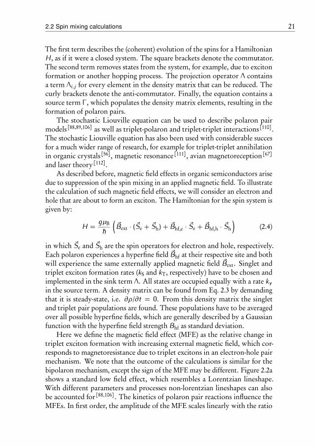
Here we define the magnetic field effect (MFE) as the relative change intriplet exciton formation with increasing external magnetic field, which cor-responds to magnetoresistance due to triplet excitons in an electron-hole pairmechanism. We note that the outcome of the calculations is similar for thebipolaron mechanism, except the sign of the MFE may be different. Figure 2.2ashows a standard low field effect, which resembles a Lorentzian lineshape.With different parameters and processes non-lorentzian lineshapes can alsobe accounted for [88,106]. The kinetics of polaron pair reactions influence theMFEs. In first order, the amplitude of the MFE scales linearly with the ratio
22 Chapter 2 : Modelling organic magnetoresistance
ba
dc
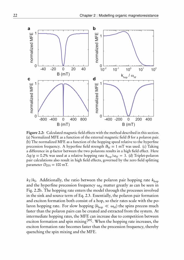
Figure 2.2: Calculated magnetic field effects with the method described in this section.(a) Normalized MFE as a function of the external magnetic field B for a polaron pair.(b) The normalized MFE as a function of the hopping speed relative to the hyperfineprecession frequency. A hyperfine field strength Bhf = 1 mT was used. (c) Takinga difference in g-factor between the two polarons results in a high field effect. Here∆g/g = 0.2% was used at a relative hopping rate khop/ωhf = 3. (d) Triplet-polaronpair calculations also result in high field effects, governed by the zero field splittingparameter DZFS = 100 mT.
kT/kS. Additionally, the ratio between the polaron pair hopping rate khopand the hyperfine precession frequency ωhf matter greatly as can be seen inFig. 2.2b. The hopping rate enters the model through the processes involvedin the sink and source term of Eq. 2.3. Essentially, the polaron pair formationand exciton formation both consist of a hop, so their rates scale with the po-laron hopping rate. For slow hopping (khop � ωhf) the spins precess muchfaster than the polaron pairs can be created and extracted from the system. Atintermediate hopping rates, the MFE can increase due to competition betweenexciton formation and spin mixing[89]. When the hopping rate increases, theexciton formation rate becomes faster than the precession frequency, therebyquenching the spin mixing and the MFE.
2.3 Drift-diffusion model 23
The stochastic Liouville equation is useful to calculate the MFEs of differentmechanisms. For the bipolaron mechanism, the approach is approximately thesame as for electron-hole pairs, althought different parameters may be selected.The ∆g-mechanism can readily be calculated by taking unequal g-factors for theelectron and hole in Eq. 2.4. The ∆g-mechanism leads to additional spin mixingwith increasing magnetic field, resulting in a high field effect as illustrated inFig. 2.2c. However, the ∆g-mechanism only works if the spin mixing is already(slightly) suppressed, for example, because of intermediate hopping or an S-T0energy splitting due to spin-spin interactions. Besides polaron pairs, spin mixingof triplet-polaron or triplet-triplet pairs can be calculated with the stochasticLiouville equation, generally resulting in high field effects governed by thezero field splitting of the triplet exciton. An example of such a calculation isshown in Fig. 2.2d. In chapter 6, we will use such calculations to investigate theanisotropy of high field effects in greater detail.
To summarize, we have shown that a density matrix formalism usingthe stochastic Liouville equation of a two site model is capable of describingmagnetic field effects in organic semiconductors arising from microscopicprocesses, such as polaron pair spin mixing, triplet-polaron spin mixing andthe ∆g-mechanism. However, another question is how the charge transportproperties of the devices, and thus the magnetoresistance, depend on thesemicroscopic changes. In the next section, we use a straightforward numericaldevice model to shed more light on the influence of the device physics oforganic magnetoresistance.
2.3 Drift-diffusion model
Organic semiconductor devices are complex, disordered systems. Finding anaccurate and reliable numerical description of these materials is a complicatedand on-going field of research. In this thesis, we gain insight into the con-ductive properties and current-voltage behavior of such devices by employinga numerical model solving the drift-diffusion, continuity and Poisson equa-tions[113–116]. We use a finite element method where the equations are solvedusing forward integration in time until steady state is obtained. The organicmaterial is described as an effective medium with a dielectric constant εr .
The model describes the transport of the electron and hole polarons, withdensities n and p respectively. Electrons and holes have an effective mobilityµn and µp respectively, which describes how fast they can move through theorganic semiconductor. The actual transport can be divided into two contri-butions: drift and diffusion. Drift of charged particles arises from the forceexerted onto them by an electric field F , which can also be described by theelectrostatic potential φ within the device as F = −∇φ. Diffusion is a result
24 Chapter 2 : Modelling organic magnetoresistance
of particles moving due to a difference in concentration. The electron (hole)current Jn(p) can then be defined as the sum of both drift and current as:
Jn = qµnn∇φ + qDn∇n,Jp = qµpp∇φ − qDp∇p,
(2.5)
in which Dn(p) is the electron (hole) diffusion constant, which is generallygiven by the Einstein equation Dn(p) = kBT /qµn(p). Here q is the elementarycharge, kB is the Boltzmann constant and T is the temperature. The continuityequations then describe how the particle densities actually change in time:
∂n∂t = 1
q∇Jn − rpreγnp,∂p∂t = − 1
q∇Jp − rpreγnp,(2.6)
These contain a contribution due to charge transport and due to electron-hole recombination. For recombination we assume bimolecular Langevinrecombination[18] with a coefficient γ = q(µn + µp)/εrε0 [117], where ε0 is thevacuum permittivity. This means the recombination is considered a diffusiveprocess, where the rate is solely determined by the ability of the electronand hole to find each other. The equations also contain a prefactor which isconsidered rpre = 1 for a pure Langevin process. In the next chapter we willalso investigate trap-assisted recombination processes. Additionally, a devicemodel has to take the Poisson equation into consideration:
εrε0∇2φ = q(n− p), (2.7)
which describes how the electrostatic potential varies with the charge distribu-tion.
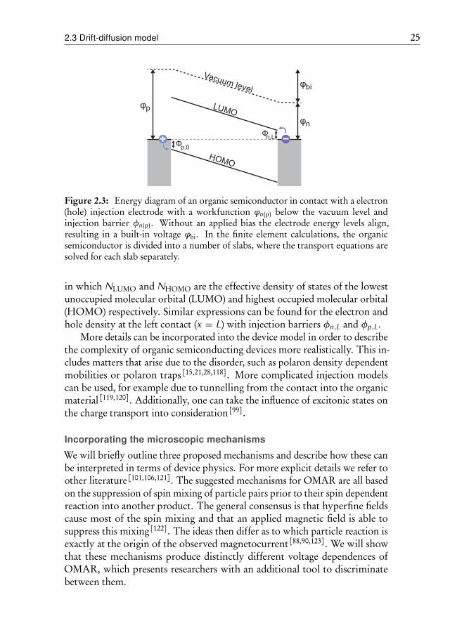
In order to obtain a unique solution to the system of coupled differentialequations given by Eq. (2.5-2.7) one needs to define the boundary conditions,i.e. the carrier densities and potential at the contacts. As illustrated in Fig.2.3the boundary conditions are relatively straightforward for a one-dimensionalmodel. Then the potential φ(x) simply reads:
φ(L)− φ(0) = φbi − Va, (2.8)
in which the built-in potential φbi is given by the difference of the electrodework functions, Va is the applied voltage over the contacts and L is the thichnessof the semiconductor layer. The boundary condition for the charge density ateach contact is generally given by the contact barrier and Boltzmann statistics.For the electron and hole density at the left contact (x = 0) with injectionbarriers φn,0 and φp,0 respectively, this results in:
n(0) = NLUMOe−φn,0kBT ,
p(0) = NHOMOe−φp,0kBT ,
(2.9)
2.3 Drift-diffusion model 25
φ
LUMO
HOMO
Vacuum level
Φ
n
n,L
φp
Φ p,0
φbi
Figure 2.3: Energy diagram of an organic semiconductor in contact with a electron(hole) injection electrode with a workfunction φn(p) below the vacuum level andinjection barrier φn(p). Without an applied bias the electrode energy levels align,resulting in a built-in voltage φbi. In the finite element calculations, the organicsemiconductor is divided into a number of slabs, where the transport equations aresolved for each slab separately.
in which NLUMO and NHOMO are the effective density of states of the lowestunoccupied molecular orbital (LUMO) and highest occupied molecular orbital(HOMO) respectively. Similar expressions can be found for the electron andhole density at the left contact (x = L) with injection barriers φn,L and φp,L.
More details can be incorporated into the device model in order to describethe complexity of organic semiconducting devices more realistically. This in-cludes matters that arise due to the disorder, such as polaron density dependentmobilities or polaron traps[15,21,28,118]. More complicated injection modelscan be used, for example due to tunnelling from the contact into the organicmaterial[119,120]. Additionally, one can take the influence of excitonic states onthe charge transport into consideration[99].
Incorporating the microscopic mechanisms
We will briefly outline three proposed mechanisms and describe how these canbe interpreted in terms of device physics. For more explicit details we refer toother literature [101,106,121]. The suggested mechanisms for OMAR are all basedon the suppression of spin mixing of particle pairs prior to their spin dependentreaction into another product. The general consensus is that hyperfine fieldscause most of the spin mixing and that an applied magnetic field is able tosuppress this mixing[122]. The ideas then differ as to which particle reaction isexactly at the origin of the observed magnetocurrent [88,90,123]. We will showthat these mechanisms produce distinctly different voltage dependences ofOMAR, which presents researchers with an additional tool to discriminatebetween them.
26 Chapter 2 : Modelling organic magnetoresistance
The first mechanism to be included in our device model is the bipolaronmechanism, which has been described elaborately in the literature[88]. Essen-tially, it is based on spin blocking of polarons of the same charge and it statesthat this spin blocking increases when a magnetic field is applied. In principlethis implies the formation of bipolarons, however, these are not necessarily con-sidered to have a significant lifetime. Therefore, we do not need to incorporatean actual bipolaron density in our device model. We incorporate the bipolaronmechanism as a magnetic field dependent mobility of the electrons or holes inthe device. Such a method has already been investigated in previous researchin order to model the MC(V ) for an unbalanced charge injecting device[124].Here we will use this method to simulate the behaviour of a more standarddevice with Ohmic contacts. We then assume that the MC is caused by areduction of the electron (or hole) mobility µn(p) and calculate the normalizedmagnetocurrent (NMC) as:
NMCn(p) = ∆JJ
µn(p)∆µn(p) , (2.10)
where we emphasize that ∆µn(p) is negative in all our studies.Many devices used for magnetoresistance measurements contain both elec-
trons and holes under typical operational conditions. The electron-hole mecha-nism describes how reactions between these carriers can lead to a magnetic fieldeffect[90]. The electrons and holes can recombine together to form excitons oreven recombine directly to the ground state in some cases. This process is spindependent, since the electron-hole pair that is formed in the process can eitherhave a singlet or triplet spin state. When the recombination or dissociationrates are different for the singlet and triplet state, a magnetic field will effectivelyreduce the total recombination rate of the electrons and holes[90,92]. This canbe incorporated in a device model as a reduced recombination mobility µr ofthe charge carriers. Because µr = rpre(µn + µp)[124], a change in recombina-tion can be calculated straightforwardly with a change in the recombinationprefactor rpre. The NMC can then be defined as:
NMCr = ∆JJ
rpre∆rpre, (2.11)
The last mechanism we outline deals with triplet exciton-polaron reactions.Triplet excitons generally have a much longer lifetime than singlet excitons andwill therefore probably be more abundant in a device. Therefore, these tripletexcitons have a larger probability to interact and react with polarons in thedevice. Since the singlet/triplet formation fraction is believed to be magneticfield dependent[89], then so is their influence on the polaron transport. This
2.3 Drift-diffusion model 27
concept is the basis of the triplet-polaron mechanism for OMAR, which wasfirst stated in literature by Desai et al.[123]
Their contemporary triplet-polaron interaction mechanism simply statesthat triplet excitons temporarily captures free polarons, however, no quanti-tative model has so far been presented to describe such an effect. Recently, itwas suggested that the actual formation of charged excitons[125], also knownas trions [105], could be at the origin of OMAR[100,126,127]. Since these trionsare assumed to have a very small or even no mobility, they effectively act astrap states for the polarons. We do note that the actual concept and specificmicroscopic details of the trion relevant for OMAR, such as the exact spincoupling, are still under debate[126]. For the purpose of our simulations, it caneither be seen as a loosely bound triplet-polaron pair or an actual particle. Inour device model we will keep track of the exciton and trion density, where weassume that a magnetic field will reduce the formation probability of tripletexcitons. This will in turn reduce the trion density and thereby enhance thefree polaron density, leading to a magnetocurrent.
For the triplet-polaron mechanism we incorporate the continuity equa-tions of the triplet exciton and trion density into our device model, wherethe excitons are created from electron-hole recombination and the trions fromtriplet exciton-polaron reactions. This also implies the incorporation of addi-tional recombination and generation terms into the electron and hole polaroncontinuity equations. First of all we consider the formation of triplet excitonsfrom the electron and hole recombination rate rpreγnpwith a triplet formationprobability PT, which results in a continuity equation for the triplet excitondensity nT:
∂nT
∂t = PTrpreγnp− γTPnT(n+ p)− kTnT. (2.12)
Triplet excitons can undergo a reaction with polarons which is defined by thetriplet-polaron coefficient γTP or they can recombine directly to the groundstate with a rate kT. Subsequently, negative trions ntrion and positive trionsptrion can be formed from the triplet-polaron reaction according to:
∂ntrion∂t = γTPnTn− ktrionntrion,
∂ptrion∂t = γTPnTp− ktrionptrion,
(2.13)
in which ktrion is their decay rate back into a free polaron. Due to theseprocesses one needs to modify the electron and hole continuity equations into:
∂n∂t = 1
q∇Jn − rpreγnp− γTPnTn+ ktrionntrion,∂p∂t = − 1
q∇Jp − rpreγnp− γTPnTp+ ktrionptrion.(2.14)
28 Chapter 2 : Modelling organic magnetoresistance
In addition, the Poisson equation has to account for the charge of the trions:
εrε0∇2φ = q(n− p+ ntrion − ptrion), (2.15)
A magnetic field will reduce the formation of triplet excitons[89], which can beincorporated into our model as a reduction of PT. Therefore, the NMC forthe triplet polaron mechanism is given by:
NMCTP = ∆JJ
1∆PT. (2.16)
Material parameters for γTP and kT can be taken from experimental workavailable in the literature[98,99,105,119,128,129].
Device model results
Using the device model introduced in the previous section, we will investigatethe simulated effect of a magnetic field on the current through an organicsemiconductor. We take electrode work functions that almost match theHOMO and LUMO for each injecting electrode, respectively, with contactbarriers of 0.1 eV, which should correspond to Ohmic contacts and resultsin balanced bipolar charge injection [113]. For the bulk of the device we willconsider a straightforward low mobility semiconductor, inspired by poly(p-phenylene vinylene) (PPV), with equal electron and hole mobilities µn = µp= 10−6 cm2Vs−1 and with a bandgap of 2.8 eV. Here we note that an electronand hole mobility orders of magnitude different have been reported in manysemiconducting organic materials, such as PPV[130] and Alq3 [131]. However, arecent study by Zhang et al.[24] has shown that the intrinsic mobility of thefree electrons and holes is approximately the same. The apparent differencearises from trapping of free polarons (electrons in the case of PPV), masking theintrinsic transport properties and at first sight leading to an effective reductionof mobility. In the next chapter, the influence of traps on the device andtriplet-polaron reactions will also be investigated.
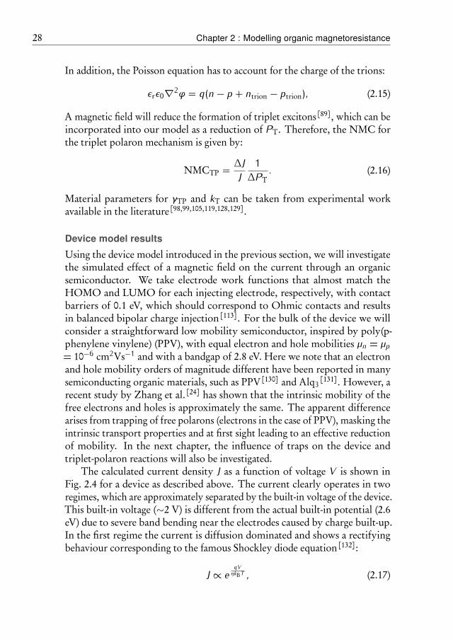
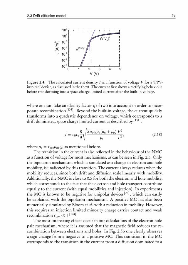
The calculated current density J as a function of voltage V is shown inFig. 2.4 for a device as described above. The current clearly operates in tworegimes, which are approximately separated by the built-in voltage of the device.This built-in voltage (∼2 V) is different from the actual built-in potential (2.6eV) due to severe band bending near the electrodes caused by charge built-up.In the first regime the current is diffusion dominated and shows a rectifyingbehaviour corresponding to the famous Shockley diode equation[132]:
J ∝ eqVηkBT , (2.17)
2.3 Drift-diffusion model 29
0 1 2 3 4 510-9
10-7
10-5
10-3
10-1
101
103
J (A
/m2 )
V (V)
eqV/2kBT
(V-Vbi)2
Figure 2.4: The calculated current density J as a function of voltage V for a ’PPV-inspired’ device, as discussed in the thext. The current first shows a rectifying behaviourbefore transforming into a space charge limited current after the built-in voltage.
where one can take an ideality factor η of two into account in order to incor-porate recombination[133]. Beyond the built-in voltage, the current quicklytransforms into a quadratic dependence on voltage, which corresponds to adrift dominated, space charge limited current as described by[134]:
J = ε0εr89√2πµnµp(µn + µp)
µr
V 2L3 , (2.18)
where µr = rpreµnµp, as mentioned before.The transition in the current is also reflected in the behaviour of the NMC
as a function of voltage for most mechanisms, as can be seen in Fig. 2.5. Onlythe bipolaron mechanism, which is simulated as a change in electron and holemobility, is unaffected by this transition. The current always reduces when themobility reduces, since both drift and diffusion scale linearly with mobility.Additionally, the NMC is close to 0.5 for both the electron and hole mobility,which corresponds to the fact that the electron and hole transport contributeequally to the current (with equal mobilities and injection). In experimentsthe MC is known to be negative for unipolar devices[78], which can easilybe explained with the bipolaron mechanism. A positive MC has also beennumerically simulated by Bloom et al. with a reduction in mobility. However,this requires an injection limited minority charge carrier contact and weakrecombination rpre � 1[124].
The most interesting effects occur in our calculations of the electron-holepair mechanism, where it is assumed that the magnetic field reduces the re-combination between electrons and holes. In Fig. 2.5b one clearly observesa sign change from a negative to a positive MC. This transition in the MCcorresponds to the transition in the current from a diffusion dominated to a
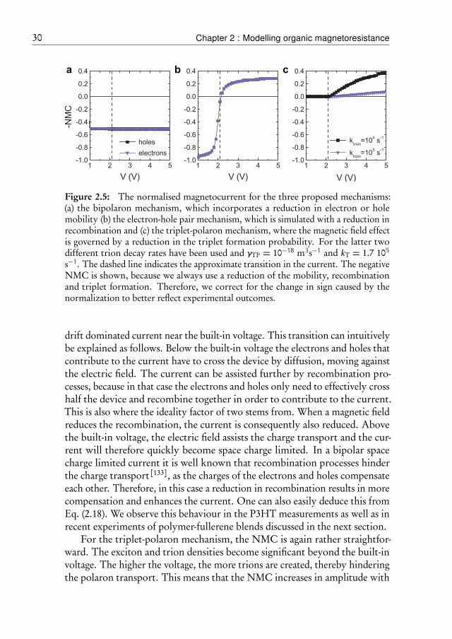
30 Chapter 2 : Modelling organic magnetoresistance
a b c
Figure 2.5: The normalised magnetocurrent for the three proposed mechanisms:(a) the bipolaron mechanism, which incorporates a reduction in electron or holemobility (b) the electron-hole pair mechanism, which is simulated with a reduction inrecombination and (c) the triplet-polaron mechanism, where the magnetic field effectis governed by a reduction in the triplet formation probability. For the latter twodifferent trion decay rates have been used and γTP = 10−18 m3s−1 and kT = 1.7 105s−1. The dashed line indicates the approximate transition in the current. The negativeNMC is shown, because we always use a reduction of the mobility, recombinationand triplet formation. Therefore, we correct for the change in sign caused by thenormalization to better reflect experimental outcomes.
drift dominated current near the built-in voltage. This transition can intuitivelybe explained as follows. Below the built-in voltage the electrons and holes thatcontribute to the current have to cross the device by diffusion, moving againstthe electric field. The current can be assisted further by recombination pro-cesses, because in that case the electrons and holes only need to effectively crosshalf the device and recombine together in order to contribute to the current.This is also where the ideality factor of two stems from. When a magnetic fieldreduces the recombination, the current is consequently also reduced. Abovethe built-in voltage, the electric field assists the charge transport and the cur-rent will therefore quickly become space charge limited. In a bipolar spacecharge limited current it is well known that recombination processes hinderthe charge transport[133], as the charges of the electrons and holes compensateeach other. Therefore, in this case a reduction in recombination results in morecompensation and enhances the current. One can also easily deduce this fromEq. (2.18). We observe this behaviour in the P3HT measurements as well as inrecent experiments of polymer-fullerene blends discussed in the next section.
For the triplet-polaron mechanism, the NMC is again rather straightfor-ward. The exciton and trion densities become significant beyond the built-involtage. The higher the voltage, the more trions are created, thereby hinderingthe polaron transport. This means that the NMC increases in amplitude with
2.4 Tuning the mechanisms in experiments 31
voltage. Because we assume that the triplet formation probability is reducedin a magnetic field, the current is enhanced, resulting in a positive MC. Ad-ditionally, the NMC increases when we reduce the trion decay rate. A rapidincrease of the MC with voltage is often observed in organic light emittingdevices[81,135], however, this is generally accompanied by a slower decrease athigh voltages. In the next chapter, we suggest that this is due to the fact thattrions are created at trap sites. This means that only a limited number of trionscan be formed, and upon filling the traps the MC will thus diminish at highvoltages.
To summarize, we have performed numerical drift-diffusion device simula-tions to study the effect of device physics on different organic magnetoresistancemechanisms. The bipolaron mechanism was simulated with a reduction inpolaron mobility, while for the electron-hole pair mechanism this was obtainedwith a reduction in recombination. The triplet-polaron mechanism requiredthe addition of continuity equations for the triplet and trion densities into thedevice model, which is the first effort to quantitatively analyse this mechanismin numerical device models as far as we know. This approach allowed us tostudy the effect of a reduction of the triplet formation probability on thecurrent as a function of voltage. We found that device physics can have a signif-icant effect on the behaviour of the magnetocurrent with voltage. Especially,the transition from a diffusion dominated to a drift dominated current has atremendous effect on the MC and can even explain sign changes observed inliterature. More complex devices and reactions can be studied by implement-ing them into this simulation method, which will allow us to further unravelthe physics behind organic magnetoresistance. The results suggest that theMC(V ) can be used as a fingerprint to identify the underlying mechanism thatdominates OMAR in a specific device, whereas the MC(B) lineshape is ofteninconclusive.
2.4 Tuning the mechanisms in experiments
As described before, several mechanisms have been suggested to explain organicmagnetoresistance. These mechanisms all rely on spin selective reactions be-tween pairs of particles, where a magnetic field suppresses the spin mixing ofthe particle pairs prior to the reaction, thereby changing the spin fraction andthe outcome. The principal question is now which particle pairs and subse-quent reactions are dominating the magnetic field effect. Most experimentalstudies have focused on trying to isolate a certain mechanism, e.g. by creatinga device where only one type of polaron is present, but a magnetoresistiveresponse was always observed and no mechanism could be excluded. So farthe largest effects have been observed in organic light emitting materials anddevices, where all particle reactions can potentially occur.
32 Chapter 2 : Modelling organic magnetoresistance
LFE
HFE
exciton PCBM
Regime 1: doping Regime 2: percolation Regime 3: two phases
CT state
Δμr
Δμr
Δμp
Δμr & Δμ
p
a b c
d e f
g h i
Figure 2.6: (a-c) Illustrations of the three different morphological regimes withincreasing PCBM concentration x and their relevant influence on the polarons. (a) Atlow x (< 20 wt.%), the PCBM acts as a dopant that quenches excitons, thereby reducingthe exciton density and exciton-polaron interactions. (b) At intermediate x (20 wt.% -60 wt.%), the PCBM forms percolative pathways for efficient electron transport. Allelectrons are thus on the PCBM, and electron-hole reactions result in charge transfer(CT) states and no excitons are present. (c) At high x (> 60 wt.%), two distinct materialphases are formed that result in seperate electron and hole transport. (d-i) Typicalmagnetoconductance (MC) results for the three regimes. (d-f) The MC as a function ofapplied field B, where the low and high field components are indicated with a blue andred line, respectively. (g-i) The MC as a function of applied voltage, where the linesdepict simulation results for the triplet-polaron mechanism in (g), the electron-holerecombination mechanism (∆µr) and the bipolaron mechanism (for holes, ∆µp). Forintermediate x, the results can be explained entirely with the electron-hole mechanism,while in the phase-separated regime a bipolaron mechanisms needs to be incorporatedas well. For the materials parameters in the simulations, we used those known for theblends, which can be found in Ref. [80].
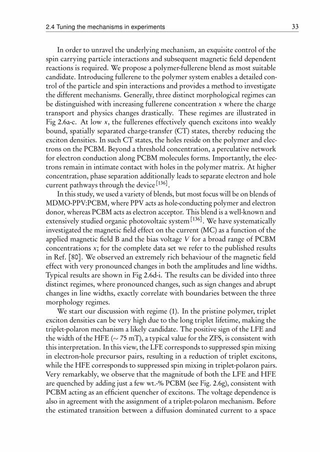
2.4 Tuning the mechanisms in experiments 33
In order to unravel the underlying mechanism, an exquisite control of thespin carrying particle interactions and subsequent magnetic field dependentreactions is required. We propose a polymer-fullerene blend as most suitablecandidate. Introducing fullerene to the polymer system enables a detailed con-trol of the particle and spin interactions and provides a method to investigatethe different mechanisms. Generally, three distinct morphological regimes canbe distinguished with increasing fullerene concentration x where the chargetransport and physics changes drastically. These regimes are illustrated inFig 2.6a-c. At low x, the fullerenes effectively quench excitons into weaklybound, spatially separated charge-transfer (CT) states, thereby reducing theexciton densities. In such CT states, the holes reside on the polymer and elec-trons on the PCBM. Beyond a threshold concentration, a perculative networkfor electron conduction along PCBM molecules forms. Importantly, the elec-trons remain in intimate contact with holes in the polymer matrix. At higherconcentration, phase separation additionally leads to separate electron and holecurrent pathways through the device[136].
In this study, we used a variety of blends, but most focus will be on blends ofMDMO-PPV:PCBM, where PPV acts as hole-conducting polymer and electrondonor, whereas PCBM acts as electron acceptor. This blend is a well-known andextensively studied organic photovoltaic system[136]. We have systematicallyinvestigated the magnetic field effect on the current (MC) as a function of theapplied magnetic field B and the bias voltage V for a broad range of PCBMconcentrations x; for the complete data set we refer to the published resultsin Ref. [80]. We observed an extremely rich behaviour of the magnetic fieldeffect with very pronounced changes in both the amplitudes and line widths.Typical results are shown in Fig 2.6d-i. The results can be divided into threedistinct regimes, where pronounced changes, such as sign changes and abruptchanges in line widths, exactly correlate with boundaries between the threemorphology regimes.
We start our discussion with regime (1). In the pristine polymer, tripletexciton densities can be very high due to the long triplet lifetime, making thetriplet-polaron mechanism a likely candidate. The positive sign of the LFE andthe width of the HFE (∼ 75 mT), a typical value for the ZFS, is consistent withthis interpretation. In this view, the LFE corresponds to suppressed spin mixingin electron-hole precursor pairs, resulting in a reduction of triplet excitons,while the HFE corresponds to suppressed spin mixing in triplet-polaron pairs.Very remarkably, we observe that the magnitude of both the LFE and HFEare quenched by adding just a few wt.-% PCBM (see Fig. 2.6g), consistent withPCBM acting as an efficient quencher of excitons. The voltage dependence isalso in agreement with the assignment of a triplet-polaron mechanism. Beforethe estimated transition between a diffusion dominated current to a space
34 Chapter 2 : Modelling organic magnetoresistance
charge limited current VT, the MC is essentially zero, while after VT it rapidlyincreases similar to our calculations in the previous section. The eventualreduction of the MC at higher voltages in the pure polymer will be addressedin detail in the next chapter.
Next, we will discuss regime (2). In these blends, PCBM is still homoge-neously distributed throughout the PPV, but forms percolative current pathsfor electrons. Excitons are effectively quenched and transferred into CT pairs.This would provide an ideal scenario for an electron (on PCBM) - hole (onPPV) pair mediated recombination mechanism, for which it is necessary thatthere is a finite chance for e-h pair formation as well as dissociation. Indeed, theobservation of an opposite HFE with respect to the LFE (shown in Fig 2.6e),as well as an abrupt change to a large field scale due to a ∆g-mechanism whenentering regime (2) corroborates this assignment. The extracted field scale ofapproximately 1 T agrees with experimental ge=1.9995 and gh=2.0028[137–139].Additionally, we observed a sudden and significant reduction of Bhf , for moredetails see Ref. [80]. This reduction is naturally explained by the very smallhyperfine field coupling that electrons experience on the fullerene cages due tothe vanishing nuclear magnetic moment of 12C. Again, the voltage dependenceshown in Fig 2.6h agrees with the assignment of an electron-hole recombinationmechanism, where a sign change occurs around the transition from a diffusiondominated to a space charge limited current as can be described with a changein recombination mobility µr in a device simulation of the blend.
Finally, in regime (3) the blends are separated into two phases. The electronsare primarily transported through a PCBM phase and the holes through a mixedphase of PPV and PCBM. With separate current paths for electrons and holes,locally the device will perform as a single carrier device. Thus, the bipolaronmechanism, the only mechanism not relying on charge carriers with oppositecharges, is expected to become dominant over the e-h pair mechanism in phase-separated blends. Indeed, we observe that the LFE is negative at all voltagesand we observe a quenching of the HFE caused by the ∆g-mechanism. Toexplain the voltage dependence with device simulations, in contrast to thehomogeneous blends, a bipolaron contribution in the form of a change in(hole) mobility µp needs to be taken into consideration.
Experimental methods
In this work we studied the magnetic field effects on the current for de-vices consisting of a blend of poly[(2-methoxy-5-(3,7-dimethyloctyloxy))-1,4-phenylenevinylene] (MDMO-PPV) and [6,6]-phenyl-C61-butyric acid methylester (PCBM). The MDMO-PPV was purchased from American Dye SourceInc. and the PCBM (>99% pure) from Solenne B.V. The devices were pre-pared on glass substrates with patterned indium tin oxide (ITO) anodes. After
2.4 Tuning the mechanisms in experiments 35
careful cleaning, followed by a UV-ozone treatment, a thin layer of poly(3,4-ethylenedioxythipophene):poly(styrenesulfonate) (PEDOT:PSS) was appliedby spin coating. The MDMO-PPV and PCBM were both dissolved in or-thodichlorobenzene, with a concentration of 10 mg/ml and 20 mg/ml respec-tively, and stirred on a hot plate at 50 ◦C for at least 2 hours after appropriateblending. The blends were spin coated at 1200 rpm for 60 s. Subsequently,the samples were transferred to a nitrogen filled glove box where the cathode,consisting of LiF and Al, was evaporated in a high vacuum system ( 10−7 mbar).From this point on, the samples always remain in a dry nitrogen environment.The total junction stack thus consisted of ITO/PEDOT:PSS(60 nm)/[PPV1−x -PCBMx](∼80 nm)/LiF(1 nm)/Al(100 nm), with x the PCBM concentration inwt.%.
Magnetic field effect measurements were performed in a cryostat that isattached to a glovebox with a nitrogen environment ([O2] <0.3 ppm, [H2O]<0.3 ppm). The cryostat is placed between the poles of an electromagnet. Themeasurements described in this article were performed at room temperature.The devices were driven at a constant voltage V using a Keithley 2400 SeriesSourceMeter. We measured the current I through the device while sweepingthe magnetic field B. From this measurement, the magnetoconductance (MC)was calculated with MC(B) = [I(B)− I(0)]/I(0).Conclusion
In this section we presented a proof of concept study, unravelling the roleof the relevant particle pairs and their reactions for OMAR. We succeededin fully correlating pronounced changes in the magnetic field effects to thecomplementary (spin) physics in the different polymer-fullerene concentrationregimes. Using the microscopic and numerical device simulations togetherwith a detailed experimental analysis, we unravel the dominant underlyingmechanisms of OMAR and can explain linewidths and sign changes herein.The results show the generic strength of the numerical tools described in thischapter. These tools will be an integral part of all further research presented inthis thesis.

3Traps and trions as origin oforganic magnetoresistance
The large effect of a small magnetic field on the current (MC) in organic semiconduc-tors, so called organic magnetoresistance (OMAR), has puzzled the field of organicspintronics during the last decade. Although the microscopic mechanisms regardingspin mixing are well understood by now, it is still unknown which pairs of spincarrying particles are influencing the current in such a drastic manner. Here, amodel for the MC is presented based on the spin selective formation of metastabletrions from triplet exciton-polaron pairs. Additionally, the magnetic field andvoltage dependence of the MC is experimentally investigated in materials showinglarge effects. Using a combination of analytical and numerical calculations, it isshown that the MC is perfectly described by a process where trions are created atpolaron trap sites.
Published as: M. Cox et al., Phys. Rev. B 88, 035202 (2013)
37
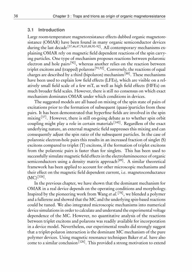
38 Chapter 3 : Traps and trions as origin of organic magnetoresistance
3.1 Introduction
Large room-temperature magnetoresistance effects dubbed organic magnetore-sistance (OMAR) have been found in many organic semiconductor devicesduring the last decade[37,46,47,78,83,88,90–92]. All contemporary mechanisms ex-plaining OMAR rely on magnetic field dependent reactions of the spin carry-ing particles. One type of mechanism proposes reactions between polaronicelectron and hole pairs[90], whereas another relies on the reaction betweentriplet excitons and (trapped) polarons [91,92]. Conversely, the reactions of equalcharges are described by a third (bipolaron) mechanism[88]. These mechanismshave been used to explain low field effects (LFEs), which are visible on a rel-atively small field scale of a few mT, as well as high field effects (HFEs) onmuch broader field scales. However, there is still no consensus on which exactmechanism dominates OMAR under which conditions in devices.
The suggested models are all based on mixing of the spin state of pairs ofexcitations prior to the formation of subsequent (quasi-)particles from thesepairs. It has been demonstrated that hyperfine fields are involved in the spinmixing[37]. However, there is still on-going debate as to whether spin orbitcoupling might play a role in certain materials[140]. Regardless of the exactunderlying nature, an external magnetic field suppresses this mixing and canconsequently adjust the spin ratio of the subsequent particles. In the case ofpolaronic electron-hole pairs this results in an increased fraction of singlet (S)excitons compared to triplet (T) excitons, if the formation of triplet excitonsfrom the polaronic pairs is faster than for singlets. This has been used tosuccessfully simulate magnetic field effects in the electroluminescence of organicsemiconductors using a density matrix approach[89]. A similar theoreticalframework has been applied to account for other microscopic mechanisms andtheir effect on the magnetic field dependent current, i.e. magnetoconductance(MC)[106].
In the previous chapter, we have shown that the dominant mechanism forOMAR in a real device depends on the operating conditions and morphology.Inspired by the pioneering work from Wang et al.[78], we blended a polymerand a fullerene and showed that the MC and the underlying spin-based reactionscould be tuned. We also integrated microscopic mechanisms into numericaldevice simulations in order to calculate and understand the experimental voltagedependence of the MC. However, no quantitative analysis of the reactionsbetween triplet excitons and polarons was readily available for incorporationin a device model. Nevertheless, our experimental results did strongly suggestthat a triplet-polaron interaction is the dominant MC mechanism of the purepolymer devices. Using magnetic resonance techniques Baker et al. have alsocome to a similar conclusion[126]. This provided a strong motivation to extend
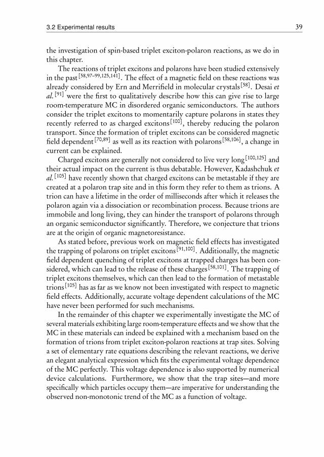
3.2 Experimental results 39
the investigation of spin-based triplet exciton-polaron reactions, as we do inthis chapter.
The reactions of triplet excitons and polarons have been studied extensivelyin the past[58,97–99,125,141]. The effect of a magnetic field on these reactions wasalready considered by Ern and Merrifield in molecular crystals[58]. Desai etal.[91] were the first to qualitatively describe how this can give rise to largeroom-temperature MC in disordered organic semiconductors. The authorsconsider the triplet excitons to momentarily capture polarons in states theyrecently referred to as charged excitons[100], thereby reducing the polarontransport. Since the formation of triplet excitons can be considered magneticfield dependent[70,89] as well as its reaction with polarons[58,106], a change incurrent can be explained.
Charged excitons are generally not considered to live very long[100,125] andtheir actual impact on the current is thus debatable. However, Kadashchuk etal.[105] have recently shown that charged excitons can be metastable if they arecreated at a polaron trap site and in this form they refer to them as trions. Atrion can have a lifetime in the order of milliseconds after which it releases thepolaron again via a dissociation or recombination process. Because trions areimmobile and long living, they can hinder the transport of polarons throughan organic semiconductor significantly. Therefore, we conjecture that trionsare at the origin of organic magnetoresistance.
As stated before, previous work on magnetic field effects has investigatedthe trapping of polarons on triplet excitons[91,100]. Additionally, the magneticfield dependent quenching of triplet excitons at trapped charges has been con-sidered, which can lead to the release of these charges[58,101]. The trapping oftriplet excitons themselves, which can then lead to the formation of metastabletrions[105] has as far as we know not been investigated with respect to magneticfield effects. Additionally, accurate voltage dependent calculations of the MChave never been performed for such mechanisms.
In the remainder of this chapter we experimentally investigate the MC ofseveral materials exhibiting large room-temperature effects and we show that theMC in these materials can indeed be explained with a mechanism based on theformation of trions from triplet exciton-polaron reactions at trap sites. Solvinga set of elementary rate equations describing the relevant reactions, we derivean elegant analytical expression which fits the experimental voltage dependenceof the MC perfectly. This voltage dependence is also supported by numericaldevice calculations. Furthermore, we show that the trap sites—and morespecifically which particles occupy them—are imperative for understanding theobserved non-monotonic trend of the MC as a function of voltage.
40 Chapter 3 : Traps and trions as origin of organic magnetoresistance
0 1 2 3 4 5
0
2
4
6
0 1 2 3 4 5
0
1
2
0 1 2 3 4 5 6 7
0
2
410-6
10-4
10-2
100
102
10-6
10-4
10-2
100
102
10-6
10-4
10-2
100
102M
CB
= 1
4 m
T (%
)
V (V)
d e
MC
B =
14
mT (%
)
V (V)
f
MC
B =
14
mT (%
)
V (V)
aJ
(A/m
2 )Alq3
PFOPPVb
J (A
/m2 )
c
J (A
/m2 )
Figure 3.1: (a-c) The current density J and the magnetic field effect on the current(MC) as a function of bias voltage V for (a) PPV, (b) PFO and (c) Alq3. The MC ismeasured at a fixed magnetic field of B = 14 mT. The solid red line is a fit with theanalytical function derived in the text.
3.2 Experimental results
All our experiments were performed on devices with a typical OLED struc-ture. We have chosen three different materials that are known to exhibite largeMC[47,72]: the co-polymer Super Yellow poly(p-phenylene vinylene) (PPV), thepolymer poly(9,9-dioctylfluorenyl-2,7-diyl) (PFO) and the small molecule tris(8-hydroxyquinoline)aluminium (Alq3). The devices are fabricated on patternedindium tin oxide glass substrates on which poly(3,4-ethylenedioxythiophene):poly(styrenesulfonate) (PEDOT:PSS) was spincoated (40 nm). PPV was dis-persed in chlorobenzene and PFO in toluene, and both were spincoated onsubstrates (90 nm). Alq3 (100 nm) was thermally evaporated onto substratesin a high vacuum system inside a nitrogen filled glovebox. After this a topelectrode consisting of LiF (1 nm)/Al (100 nm) was thermally evaporated ontoall samples in another vacuum system inside the same glovebox. All devices(active area 3 x 3 mm) were then transported inside a nitrogen environment toanother glovebox, where they were electrically and magnetically characterized.A Keithley 2400 sourcemeter is used to set a bias voltage V and measure thecurrent density J.
The J-V characteristics of the three different devices are shown in Fig. 3.1together with MC(V ) curves at a fixed magnetic field of B = 14 mT. TheMC(V ) curves are measured using a method where a fixed magnet is rotatedover the sample while sweeping the bias voltage [142]. At low voltages we alwaysobserve an Ohmic leakage current, which does not exhibit any observable
3.2 Experimental results 41
a b
c d
Figure 3.2: (a) The magnetic field effect on the current (MC) as a function themagnetic field B for Alq3, PFO and PPV. The red lines are the result of the doublenon-Lorentzian fit function and the grey dashed lines show the shape of only the lowfield effect (LFE) non-Lorentzian. (b-d) The fitted magnitude of the low and high fieldeffect as a function the bias voltage for (b) PPV, (c) PFO and (d) Alq3. The solid linesin (b-d) are analytical fits from the model derived in the text.
MC. Due to the built-in voltage caused by the different work function of theelectrodes, the devices act like a diode and suddenly turn on after a certainvoltage. This turn on voltage also seems to correspond with the observation ofa finite MC. Figure 3.1 also show the results of the low field analytical MC(V )fit function that we will derive from in the remainder of this chapter. At highvoltages and correspondingly large current densities, all devices suffer fromsevere degradation and/or significant conditioning of the MC [47], which iswhy this region is not investigated.
We have also investigated the MC as a function of applied magnetic field B.Inside the same glovebox the samples can be placed between the poles of twoelectromagnets. This allows us to measure the current while sweeping the mag-netic field. The magnetic field dependence of the current density J(B) is thencalculated with MC(B) = [J(B)− J(0)]/J(0). In order to separate the LFE andHFE, we fit the resulting MC with the sum of two empirical ‘non-Lorentzian’
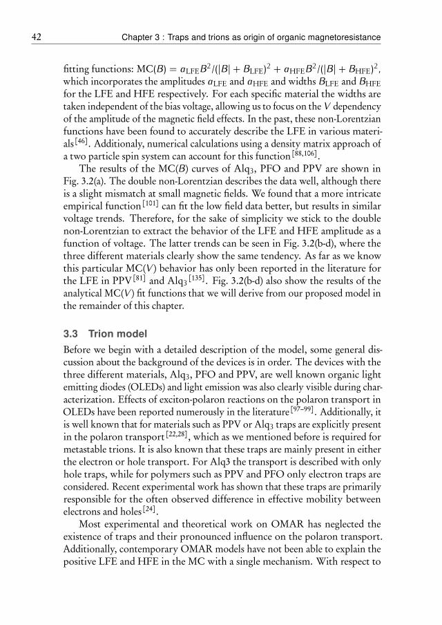
42 Chapter 3 : Traps and trions as origin of organic magnetoresistance
fitting functions: MC(B) = aLFEB2/(|B|+ BLFE)2 + aHFEB2/(|B|+ BHFE)2,which incorporates the amplitudes aLFE and aHFE and widths BLFE and BHFEfor the LFE and HFE respectively. For each specific material the widths aretaken independent of the bias voltage, allowing us to focus on the V dependencyof the amplitude of the magnetic field effects. In the past, these non-Lorentzianfunctions have been found to accurately describe the LFE in various materi-als[46]. Additionaly, numerical calculations using a density matrix approach ofa two particle spin system can account for this function[88,106].
The results of the MC(B) curves of Alq3, PFO and PPV are shown inFig. 3.2(a). The double non-Lorentzian describes the data well, although thereis a slight mismatch at small magnetic fields. We found that a more intricateempirical function[101] can fit the low field data better, but results in similarvoltage trends. Therefore, for the sake of simplicity we stick to the doublenon-Lorentzian to extract the behavior of the LFE and HFE amplitude as afunction of voltage. The latter trends can be seen in Fig. 3.2(b-d), where thethree different materials clearly show the same tendency. As far as we knowthis particular MC(V ) behavior has only been reported in the literature forthe LFE in PPV [81] and Alq3 [135]. Fig. 3.2(b-d) also show the results of theanalytical MC(V ) fit functions that we will derive from our proposed model inthe remainder of this chapter.
3.3 Trion model
Before we begin with a detailed description of the model, some general dis-cussion about the background of the devices is in order. The devices with thethree different materials, Alq3, PFO and PPV, are well known organic lightemitting diodes (OLEDs) and light emission was also clearly visible during char-acterization. Effects of exciton-polaron reactions on the polaron transport inOLEDs have been reported numerously in the literature[97–99]. Additionally, itis well known that for materials such as PPV or Alq3 traps are explicitly presentin the polaron transport[22,28], which as we mentioned before is required formetastable trions. It is also known that these traps are mainly present in eitherthe electron or hole transport. For Alq3 the transport is described with onlyhole traps, while for polymers such as PPV and PFO only electron traps areconsidered. Recent experimental work has shown that these traps are primarilyresponsible for the often observed difference in effective mobility betweenelectrons and holes[24].
Most experimental and theoretical work on OMAR has neglected theexistence of traps and their pronounced influence on the polaron transport.Additionally, contemporary OMAR models have not been able to explain thepositive LFE and HFE in the MC with a single mechanism. With respect to
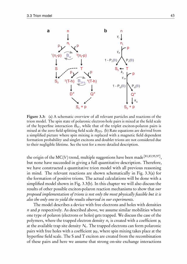
3.3 Trion model 43
1(nt-p) 3(nt-p)
nt
S
S0
T
2(T-h) 4(T-h)
Q+
Bhf
BZFS
D+
S0 + p
nt
T
Q+
S0 + p
p
p
PT(B)
PQ(B)
pp
ppS0
a bn n
1 - PT(B)
1 - PQ(B)
γR
kT
γTP
kQ
γt
Figure 3.3: (a) A schematic overview of all relevant particles and reactions of thetrion model. The spin state of polaronic electron-hole pairs is mixed at the field scaleof the hyperfine interaction Bhf , while that of the triplet exciton-polaron pairs ismixed at the zero field splitting field scale BZFS. (b) Rate equations are derived froma simplified picture where spin mixing is replaced with a magnetic field dependentformation probability and singlet excitons and doublet trions are not considered dueto their negligible lifetime. See the text for a more detailed description.
the origin of the MC(V ) trend, multiple suggestions have been made[81,83,95,97],but none have succeeded in giving a full quantitative description. Therefore,we have constructed a quantitative trion model with all previous reasoningin mind. The relevant reactions are shown schematically in Fig. 3.3(a) forthe formation of positive trions. The actual calculations will be done with asimplified model shown in Fig. 3.3(b). In this chapter we will also discuss theresults of other possible exciton-polaron reaction mechanisms to show that ourproposed implementation of trions is not only the most physically feasible but it isalso the only one to yield the results observed in our experiments.
The model describes a device with free electrons and holes with densitiesn and p respectively. As described above, we assume similar mobilities whereone type of polaron (electrons or holes) gets trapped. We discuss the case of thepolymers, where the trapped electron density nt is created with a coefficient γtat the available trap site density Nt. The trapped electrons can form polaronicpairs with free holes with a coefficient γR , where spin mixing takes place at thehyperfine field scale. The S and T exciton are created from the recombinationof these pairs and here we assume that strong on-site exchange interactions
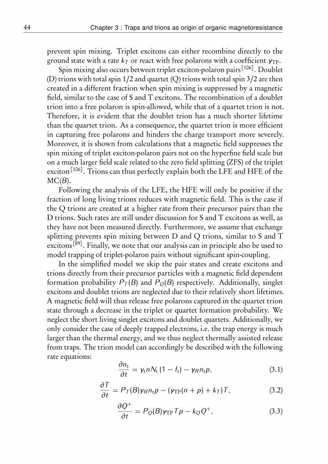
44 Chapter 3 : Traps and trions as origin of organic magnetoresistance
prevent spin mixing. Triplet excitons can either recombine directly to theground state with a rate kT or react with free polarons with a coefficient γTP.
Spin mixing also occurs between triplet exciton-polaron pairs[106]. Doublet(D) trions with total spin 1/2 and quartet (Q) trions with total spin 3/2 are thencreated in a different fraction when spin mixing is suppressed by a magneticfield, similar to the case of S and T excitons. The recombination of a doublettrion into a free polaron is spin-allowed, while that of a quartet trion is not.Therefore, it is evident that the doublet trion has a much shorter lifetimethan the quartet trion. As a consequence, the quartet trion is more efficientin capturing free polarons and hinders the charge transport more severely.Moreover, it is shown from calculations that a magnetic field suppresses thespin mixing of triplet exciton-polaron pairs not on the hyperfine field scale buton a much larger field scale related to the zero field splitting (ZFS) of the tripletexciton[106]. Trions can thus perfectly explain both the LFE and HFE of theMC(B).
Following the analysis of the LFE, the HFE will only be positive if thefraction of long living trions reduces with magnetic field. This is the case ifthe Q trions are created at a higher rate from their precursor pairs than theD trions. Such rates are still under discussion for S and T excitons as well, asthey have not been measured directly. Furthermore, we assume that exchangesplitting prevents spin mixing between D and Q trions, similar to S and Texcitons[89]. Finally, we note that our analysis can in principle also be used tomodel trapping of triplet-polaron pairs without significant spin-coupling.
In the simplified model we skip the pair states and create excitons andtrions directly from their precursor particles with a magnetic field dependentformation probability PT (B) and PQ(B) respectively. Additionally, singletexcitons and doublet trions are neglected due to their relatively short lifetimes.A magnetic field will thus release free polarons captured in the quartet trionstate through a decrease in the triplet or quartet formation probability. Weneglect the short living singlet excitons and doublet quartets. Additionally, weonly consider the case of deeply trapped electrons, i.e. the trap energy is muchlarger than the thermal energy, and we thus neglect thermally assisted releasefrom traps. The trion model can accordingly be described with the followingrate equations:
∂nt
∂t = γtnNt (1− ft)− γRntp, (3.1)
∂T∂t = PT (B)γRntp− (γTP(n+ p) + kT )T , (3.2)
∂Q+∂t = PQ(B)γTPTp− kQQ+, (3.3)
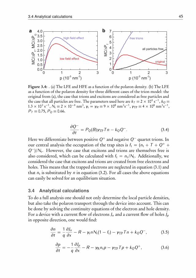
3.4 Analytical calculations 45
a b
Figure 3.4: . (a) The LFE and HFE as a function of the polaron density. (b) The LFEas a function of the polaron density for three different cases of the trion model: theoriginal from (a), the case that trions and excitons are considered as free particles andthe case that all particles are free. The parameters used here are kT = 2 × 10⁴ s−1, kQ =1.3 × 10³ s−1, Nt = 2 × 10⁻⁴ nm3, γt = γR = 9 × 10⁸ nm3s−1, γTP = 4 × 10⁸ nm3s−1,PT = 0.75, PQ = 0.66.
∂Q−∂t = PQ(B)γTPTn− kQQ−. (3.4)
Here we differentiate between positive Q+ and negative Q− quartet trions. Inour central analysis the occupation of the trap sites is ft = (nt + T + Q+ +Q−)/Nt. However, the case that excitons and trions are themselves free isalso considered, which can be calculated with ft = nt/Nt. Additionally, weconsidered the case that excitons and trions are created from free electrons andholes. This means that the trapped electrons are neglected in equation (3.1) andthat nt is substituted by n in equation (3.2). For all cases the above equationscan easily be solved for an equilibrium situation.
3.4 Analytical calculations
To do a full analysis one should not only determine the local particle densities,but also take the polaron transport through the device into account. This canbe done by solving the continuity equations of the electron and hole density.For a device with a current flow of electrons Jn and a current flow of holes Jpin opposite direction, one would find:
∂n∂t = 1
q∂Jn∂x − R − γtnNt(1− ft)− γTPTn+ kQQ−, (3.5)
∂p∂t = −1
q∂Jp∂x − R − γRntp− γTPTp+ kQQ+, (3.6)
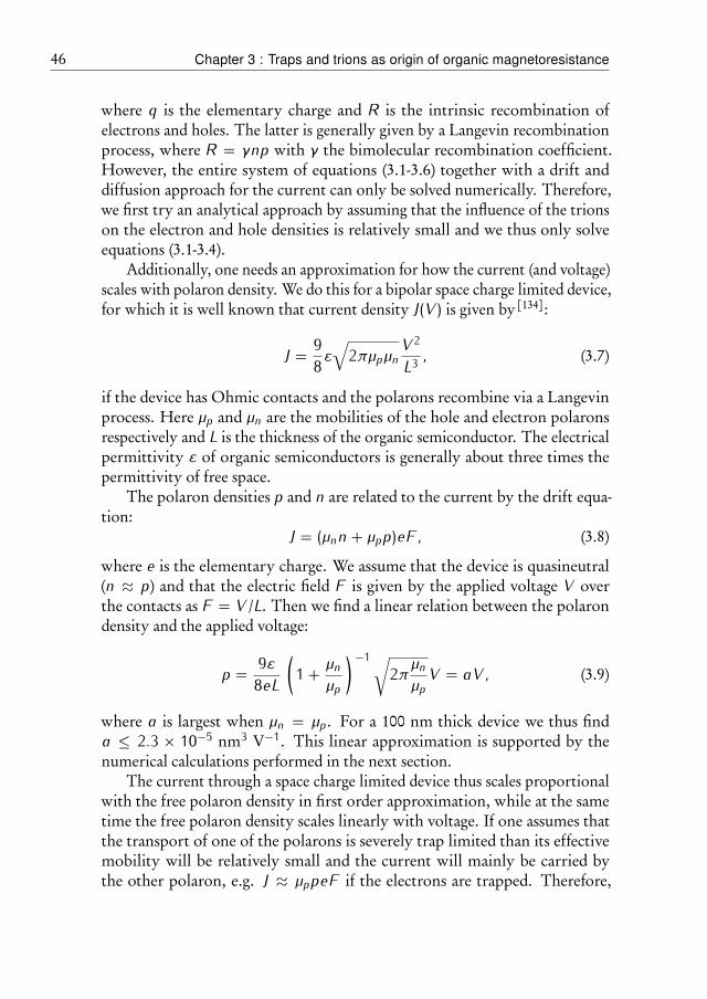
46 Chapter 3 : Traps and trions as origin of organic magnetoresistance
where q is the elementary charge and R is the intrinsic recombination ofelectrons and holes. The latter is generally given by a Langevin recombinationprocess, where R = γnp with γ the bimolecular recombination coefficient.However, the entire system of equations (3.1-3.6) together with a drift anddiffusion approach for the current can only be solved numerically. Therefore,we first try an analytical approach by assuming that the influence of the trionson the electron and hole densities is relatively small and we thus only solveequations (3.1-3.4).
Additionally, one needs an approximation for how the current (and voltage)scales with polaron density. We do this for a bipolar space charge limited device,for which it is well known that current density J(V ) is given by[134]:
J = 98ε√2πµpµnV 2L3 , (3.7)
if the device has Ohmic contacts and the polarons recombine via a Langevinprocess. Here µp and µn are the mobilities of the hole and electron polaronsrespectively and L is the thickness of the organic semiconductor. The electricalpermittivity ε of organic semiconductors is generally about three times thepermittivity of free space.
The polaron densities p and n are related to the current by the drift equa-tion:
J = (µnn+ µpp)eF, (3.8)
where e is the elementary charge. We assume that the device is quasineutral(n ≈ p) and that the electric field F is given by the applied voltage V overthe contacts as F = V /L. Then we find a linear relation between the polarondensity and the applied voltage:
p = 9ε8eL(1 + µn
µp
)−1√2πµnµpV = aV , (3.9)
where a is largest when µn = µp. For a 100 nm thick device we thus finda ≤ 2.3 × 10⁻⁵ nm3 V−1. This linear approximation is supported by thenumerical calculations performed in the next section.
The current through a space charge limited device thus scales proportionalwith the free polaron density in first order approximation, while at the sametime the free polaron density scales linearly with voltage. If one assumes thatthe transport of one of the polarons is severely trap limited than its effectivemobility will be relatively small and the current will mainly be carried bythe other polaron, e.g. J ≈ µppeF if the electrons are trapped. Therefore,
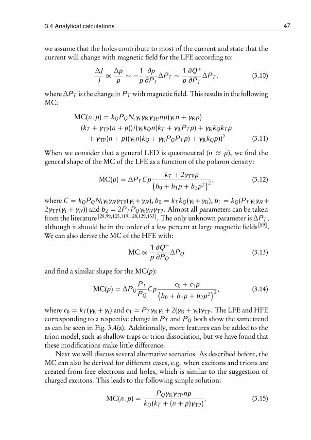
3.4 Analytical calculations 47
we assume that the holes contribute to most of the current and state that thecurrent will change with magnetic field for the LFE according to:∆J
J ∝∆pp ∼ −
1p∂p∂PT
∆PT ∼ 1p∂Q+∂PT
∆PT , (3.10)
where ∆PT is the change inPT with magnetic field. This results in the followingMC:
MC(n, p) = kQPQNtγtγRγTPnp(γtn+ γRp)(kT + γTP(n+ p))/(γtkQn(kT + γRPTp) + γRkQkTp+ γTP(n+ p)(γtn(kQ + γRPQPTp) + γRkQp))2 (3.11)
When we consider that a general LED is quasineutral (n ≈ p), we find thegeneral shape of the MC of the LFE as a function of the polaron density:
MC(p) = ∆PTCp kT + 2γTPp(b0 + b1p+ b2p2)2 , (3.12)
where C = kQPQNtγtγRγTP(γt +γR ), b0 = kT kQ(γt +γR), b1 = kQ(PTγtγR +2γTP(γt + γR )) and b2 = 2PTPQγtγRγTP. Almost all parameters can be takenfrom the literature[28,99,105,119,128,129,133]. The only unknown parameter is ∆PT ,although it should be in the order of a few percent at large magnetic fields[89].We can also derive the MC of the HFE with:
MC ∝ 1p∂Q+∂PQ
∆PQ (3.13)
and find a similar shape for the MC(p):
MC(p) = ∆PQ PTPQCp c0 + c1p(b0 + b1p+ b2p2)2 , (3.14)
where c0 = kT (γR + γt) and c1 = PTγRγt +2(γR + γt)γTP. The LFE and HFEcorresponding to a respective change in PT and PQ both show the same trendas can be seen in Fig. 3.4(a). Additionally, more features can be added to thetrion model, such as shallow traps or trion dissociation, but we have found thatthese modifications make little difference.
Next we will discuss several alternative scenarios. As described before, theMC can also be derived for different cases, e.g. when excitons and trions arecreated from free electrons and holes, which is similar to the suggestion ofcharged excitons. This leads to the following simple solution:
MC(n, p) = PQγRγTPnpkQ(kT + (n+ p)γTP) . (3.15)
48 Chapter 3 : Traps and trions as origin of organic magnetoresistance
Another possibility would be that the excitons and trions created from thetrapped electrons are free themselves and do not occupy the trap sites. In thatcase we find that:
MC(n, p) = PQNtγtγRγTPnpkQ(γRp+ γtn)(kT + (n+ p)γTP) . (3.16)
Both of these consideration lead to a monotonic increase of the MC(p) as canbe seen in Fig. 3.4(b). It is clear that only our original concept of trions resultsin a non-monotonic trend of the MC(p) in agreement with the experimentallyfound MC(V ). Additionally, another process has been considered in the lit-erature, where free triplet excitons are able to release trapped polarons[101].However, the sign of the LFE would be negative for this mechanism, as areduced fraction of triplet excitons results in less free polarons. We concludethat only the original scenario, where trions are created at the trap sites, resultsin a non-monotonic positive MC as seen in the experiment.
To finalize the analysis and find a function for the MC(V ) we now onlyneed to implement the relation between the voltage and polaron density. Asstated before, for the most trivial situation of a space charge limited device witha homogeneous electric field distribution one finds that p = a × (V − Von),where a is a constant in the order of 10−5 nm3/V. For completeness we haveadded an onset voltage Von for bipolar charge transport. We end up with ananalytical function MC(V , Von, a,∆PT ) that fits our experimental data well, ascan be seen in Fig. 3.2(b-d). Some deviations can be observed, most clearly forPFO at low voltages. A possible explanation for this will be discussed in thenext section.
3.5 Numerical calculations
In order to put some of the previous approximations on more solid ground,we have performed finite element drift diffusion calculations. As explained inchapter 1, such a method can also be used to model the voltage dependence ofmagnetic field effects by altering parameters that are presumed to be magneticfield dependent. In addition, the trion rate equations (3.1-3.4) and trion densitiescan readily be implemented in the simulation method. Here we investigatesuch an implementation with the altered continuity equations as described byeq. (3.5) and (3.6). Furthermore, the Poisson equation has to incorporate thecharge of the trapped electron and trion densities:
ε∂2φ∂x2 = q(n− p+ nt +Q− −Q+), (3.17)
where ψ is the electrostatic potential.
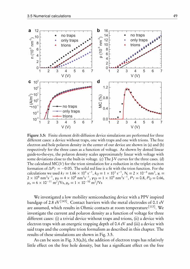
3.5 Numerical calculations 49
a b
c d
Figure 3.5: Finite element drift-diffusion device simulations are performed for threedifferent cases: a device without traps, one with traps and one with trions. The freeelectron and hole polaron density in the center of our device are shown in (a) and (b)respectively for the three cases as a function of voltage. As shown by dotted linearguide-to-the-eye, the polaron density scales approximately linear with voltage withsome deviations close to the built-in voltage. (c) The J-V curves for the three cases. (d)The calculated MC(V ) for the trion simulation for a reduction in the triplet excitonformation of ∆PT = −0.05. The solid red line is a fit with the trion function. For thecalculations we used kT = 1.66 × 10⁴ s−1, kQ = 1 × 10³ s−1, Nt = 2 × 10⁻⁴ nm3, γt =2 × 10⁸ nm3s−1, γR = 4 × 10⁸ nm3s−1, γTP = 1 × 10⁹ nm3s−1, PT = 0.8, PQ = 0.66,µn = 6 × 10⁻¹¹ m2/Vs, µp = 1 × 10⁻¹⁰ m2/Vs
We investigated a low mobility semiconducting device with a PPV inspiredbandgap of 2.8 eV[143]. Contact barriers with the metal electrodes of 0.1 eVare assumed, which results in Ohmic contacts at room temperature [113]. Weinvestigate the current and polaron density as a function of voltage for threedifferent cases: (i) a trivial device without traps and trions, (ii) a device withelectron traps with an energetic trapping depth of 0.4 eV and (iii) a device withsaid traps and the complete trion formalism as described in this chapter. Theresults of these simulations are shown in Fig. 3.5.
As can be seen in Fig. 3.5(a,b), the addition of electron traps has relativelylittle effect on the free hole density, but has a significant effect on the free
50 Chapter 3 : Traps and trions as origin of organic magnetoresistance
electron density as can be expected since traps were added to the electronchannel. The addition of trions actually has an opposite effect, as they trapholes as well, thereby rebalancing some of the charge transport. It is clearthat both the addition of traps and trions lead to a reduction of the currentin the space charge limited region after the built-in voltage, as can be seen inFig. 3.5(c).
The calculations suggest that a linear voltage dependence of the polarondensity as assumed in our analytical approach can be considered fairly reason-able. Some deviations are observed at low voltages around 2-3 V. This also leadsto changes in the shape of the MC(V ) with respect to the analytical function inthis same region as can be seen in Fig. 3.5(d). Although such deviation are alsoobserved in some of the experimental results, primarily for PFO (see Fig. 3.2(c)),they are less dramatic than in our simulations. This suggests that some effectthat is currently not considered in the numerical simulations suppresses thesenon-linearities in the real devices.
An aspect of organic materials that has not been incorporated in the devicesimulations is the energetic (and spatial) disorder. State-of-the-art drift-diffusionOLED simulations consider the Gaussian disorder of HOMO and LUMOof the organic material, by implementing electric field and polaron densitydependent mobilities [15]. Additionally, the energetic distribution of traps isalso known to be Gaussian[144,145]. Electric field dependent mobilities canassist in pushing the polarons faster into the bulk of the device, since thehighest electric fields are present at the edges of the devices. This might help toovercome the small non-linearities at lower voltages.
Finally, we note that numerical calculations involve more parameters thanour analytical derivation of the trion model, which complicates their interpreta-tion. Nevertheless, these results suggest that our analytical approximations arerealistic. This helps to identify the relevant underlying physics of the observedmagnetic field effects. The advantage of numerical calculations is that they canrelatively easily be applied to a diverse range of devices. Additionally, this workcan help to improve predictive OLED models which do not yet incorporatethe combination of triplet-polaron interactions, trions and traps.
3.6 Discussion
With the trion model in mind we are now able to intuitively explain the trend ofthe MC(V ). The initial rise of the MC with voltage is, quite straightforwardly,due to the progressive formation of trions. Because they are created from a trap-assisted recombination mechanism, the incline is relatively steep at low voltagesand scales linear with V − Von. The eventual decline is on account of trapfilling by the triplet excitons and trions. With their increasing presence they
3.7 Conclusion 51
are impeding the trapping of polarons and their own subsequent formation.As a result the number of trions stabilizes with voltage, while the free polarondensity continues to rise. The relative effect of the trions on the total currentwill diminish while the MC drops at higher voltages with (V − Von)−2.
We note that the reported weak temperature dependence of the MC [46]
does not directly interfere with the trion model, because the temperaturedependence of many processes may cancel out. For example, when it comes tothe actual formation of the trion, the (monomolecular) triplet exciton lifetimewill reduce with temperature, leading to less chance of forming a trion. Atthe same time the polaron mobility will increase, leading to a larger triplet-polaron interaction chance and thus more chances of forming a trion. Thepossible temperature dependence of a triplet-based magnetoresistance modelhas also been discussed by Zhang et al.[84], while for an electron-hole pairrecombination mechanism this has been done by Bagnich et al.[81]
In experimental studies it should be possible to enhance the MC by addingmore trap sites and thereby open the way to the engineering of efficient organicmagnetic field sensors. Interestingly, a first step on this road was recently takenin Alq3 devices by exposing them to X-rays, leading to an enhancement ofthe MC[146]. Whether this same process could be applied to other devicesis debatable as the exact nature of traps is still under investigation. Recently,an elaborate study suggested that hydrated oxygen complexes can explainthe electron traps in most semiconducting polymers[23]. In the next twochapters, we investigate how different kind of traps can influence the MC, bothexperimentally and theoretically. As a final comment it should be noted thattrions and their effect on the current have been greatly overlooked in organicdevices so far.
3.7 Conclusion
In conclusion, in this chapter we have investigated the magnetic field depen-dence of the current in several organic light emitting devices. A high fieldcontribution in the MC(B) was observed in all measured devices, which widthcan be attributed to the zero field splitting of triplet excitons. We also foundnon-monotonic trends in the MC with applied voltage in all devices, whichcan be explained with a magnetic field dependent formation of longliving ex-citations at trap sites. We can model all our experimental data well with ourproposed trion mechanism: the spin dependent formation of triplet excitons attrap sites and their subsequent spin selective reaction with free polarons intometastable trions. An analytical function was derived that fits the data welland can be used to analyze and better understand the MC in OLEDs. Thetrion model was also implemented into numerical device simulations, which

52 Chapter 3 : Traps and trions as origin of organic magnetoresistance
not only confirmed our analytical deriviations, but can ultimately be used in abroad range of predictive device simulations.
4Investigating the influence oftraps on organic magneto-resistance by molecular doping
Traps are localised, deep lying energetic states and are generally considered detri-mental for organic semiconducting devices. In this chapter we investigate theirinfluence on the magnetic field sensitive current in organic devices, an effect oftencalled organic magnetoresistance. Polymer thin films were doped with materialswell-known to influence trap characteristics in such devices. We analyzed the ob-served trends in the intrinsic magnetic field effects in terms of the trapped trionmodel from the previous chapter, which incorporates the spin dependent formationof excitations at these trap sites. The results provide strong evidence that the intrin-sic traps in the polymer material are indeed at the origin of these magnetic fieldeffects. This shows that traps have beneficial properties and that their control mayprovide an appealing route for the engineering of efficient organic magnetic fieldsensors.
Most of this chapter was published as: M. Cox et al., Phys. Rev. B 89, 085201 (2014).Section 4.4 includes new, unpublished results.
53
54 Chapter 4 : Investigating the influence of traps on OMAR by molecular doping
4.1 Introduction
Organic electronics is considered to be a field of untold possibilities [1]. How-ever, whereas the spin degree of freedom of electrons is utilized to its fullestin inorganic ’spintronic’ devices[31], organic materials are still lagging behind.This limits the use of organic materials in conjunction with many conventionalmemory and sensing applications. But in the past decade, the young fieldof organic spintronics has been catching up[91,101]. Beside the realisation ofstate-of-the-art spin injecting devices [40,44,45,147], which try to mimic spin valvetechnology, another development piqued tremendous interest. It was foundthat a small magnetic field can have a large effect on the current in organicsemiconductors—an effect that was referred to as organic magnetoresistance(OMAR)[46]. OMAR is an intrinsic effect that manifests itself at room tem-perature and magnetic fields of only a few millitesla. The changes in currentcan become as large as 25% in thin film devices[81], while very recent workeven reports on ultrahigh magnetoresistance values of over 2000% in perfectlyone dimensional molecular systems [48]. Cheap plastic sensor applications havealready been suggested as an example of its application potential[49].
The desire to unravel the underlying physics of this intrinsic magnetoresis-tance effect in organic semiconductors has initiated intense experimental andtheoretical research. Multiple mechanisms have been proposed for OMAR andrecent work shows these can all become dominant under specific conditions[80].Additionally, there is a growing awareness of the role of defects and polarontraps in the explanation of the large reported OMAR values[48,73,81,146,148,149].In this chapter, we investigate the influence of traps on OMAR more closelywith molecular dopants known from previous trap related research. Our resultsfurther strengthen the notion that traps are crucial for the large magnetic fieldeffects observed in organic semiconductors.
Although the exact influence of traps is still under debate, the origin ofOMAR is believed to lie in the spin physics occurring in organic semiconduc-tors. Nowadays, it is well established that a magnetic field can change reactionsand interactions of spin carrying particles, such as polarons and excitons, cre-ated in semiconducting polymers and molecules[60,73,80,88,89,91,95,106,124]. Whena pair of particles meets, the spin of these individual particles evolves in time,leading to mixing of the pair’s total spin state—a process in which hyperfinefields are involved[37], although in certain materials spin orbit coupling mightalso play a role[140]. A large applied magnetic field can then suppress the spinmixing and thereby influence the outcome of spin dependent reactions[89,106].We note that the organic spintronics community has already been preceded byspin chemistry, where magnetic field dependent reactions are well-known[60].For example, such mechanisms have been suggested to play a role in how birdsorient in magnetic fields, using specialized photoreceptors[68].
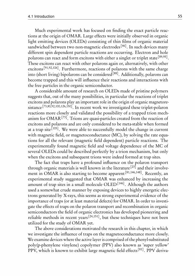
4.1 Introduction 55
Much experimental work has focused on finding the exact particle reac-tions at the origin of OMAR. Large effects were initially observed in organiclight emitting devices (OLEDs) consisting of thin films of organic materialsandwiched between two non-magnetic electrodes[46]. In such devices manydifferent spin dependent particle reactions are occurring. Electron and holepolarons can react and form excitons with either a singlet or triplet state[89,95].These excitons can react with other polarons again or, alternatively, with otherexcitons[91,92,106]. Furthermore, reactions of polarons with the same chargeinto (short living) bipolarons can be considered [88]. Additionally, polarons canbecome trapped and this will influence their reactions and interactions withthe free particles in the organic semiconductor.
A considerable amount of research on OLEDs made of pristine polymerssuggests that, out of the many possibilities, in particular the reactions of tripletexcitons and polarons play an important role in the origin of organic magnetore-sistance[73,80,92,100,126,150]. In recent work we investigated these triplet-polaronreactions more closely and validated the possibility of a trapped trion mech-anism for OMAR[73]. Trions are quasi-particles created from the reaction ofexcitons and polarons and are only considered to be meta-stable when formedat a trap site[105]. We were able to successfully model the change in currentwith magnetic field, or magnetoconductance (MC), by solving the rate equa-tions for all the relevant (magnetic field dependent) particle reactions. Theexperimentally found magnetic field and voltage dependence of the MC ofseveral OLEDs could be described perfectly by a trion mechanism, but onlywhen the excitons and subsequent trions were indeed formed at trap sites.
The fact that traps have a profound influence on the polaron transportthrough organic materials is well known in the literature [23] and their involve-ment in OMAR is also starting to become apparent[81,146,148]. Recently, anexperimental study suggested that OMAR was enhanced by increasing theamount of trap sites in a small molecule OLED [146]. Although the authorsused a somewhat crude manner by exposing devices to highly energetic elec-trons generated by X-rays, this seems as strong experimental evidence of theimportance of traps (or at least material defects) for OMAR. In order to investi-gate the effects of traps on the polaron transport and recombination in organicsemiconductors the field of organic electronics has developed pioneering andreliable methods in recent years [24,151], but these techniques have not beenutilized for the study of OMAR yet.
The above considerations motivated the research in this chapter, in whichwe investigate the influence of traps on the magnetoconductance more closely.We examine devices where the active layer is comprised of the phenyl-substitutedpoly(p-phenylene vinylene) copolymer (PPV) also known as ’super yellow’PPV, which is known to exhibit large magnetic field effects [81]. PPV deriva-
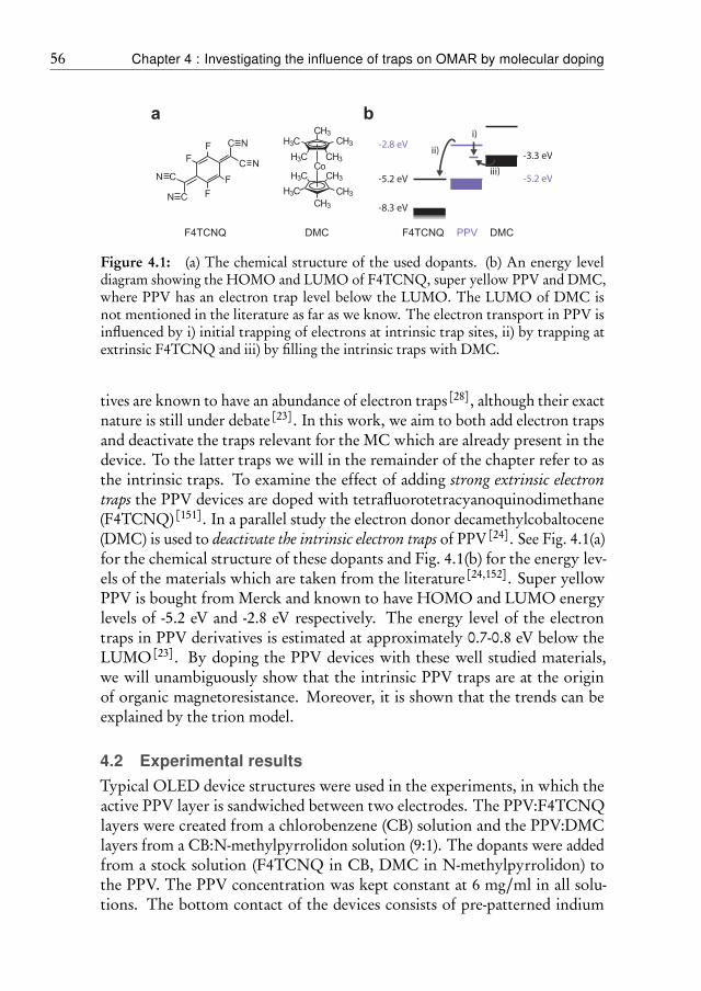
56 Chapter 4 : Investigating the influence of traps on OMAR by molecular doping
DMCF4TCNQ
a b
DMCF4TCNQ PPV
Co
CH3H3C
CH3CH3H3C
H3C
H3C
CH3
CH3
CH3
C N
C N
N C
N C
F
F
F
F
-5.2 eV
-8.3 eV
-2.8 eV
-3.3 eV
-5.2 eV
i)
ii)
iii)
Figure 4.1: (a) The chemical structure of the used dopants. (b) An energy leveldiagram showing the HOMO and LUMO of F4TCNQ, super yellow PPV and DMC,where PPV has an electron trap level below the LUMO. The LUMO of DMC isnot mentioned in the literature as far as we know. The electron transport in PPV isinfluenced by i) initial trapping of electrons at intrinsic trap sites, ii) by trapping atextrinsic F4TCNQ and iii) by filling the intrinsic traps with DMC.
tives are known to have an abundance of electron traps[28], although their exactnature is still under debate[23]. In this work, we aim to both add electron trapsand deactivate the traps relevant for the MC which are already present in thedevice. To the latter traps we will in the remainder of the chapter refer to asthe intrinsic traps. To examine the effect of adding strong extrinsic electrontraps the PPV devices are doped with tetrafluorotetracyanoquinodimethane(F4TCNQ) [151]. In a parallel study the electron donor decamethylcobaltocene(DMC) is used to deactivate the intrinsic electron traps of PPV[24]. See Fig. 4.1(a)for the chemical structure of these dopants and Fig. 4.1(b) for the energy lev-els of the materials which are taken from the literature [24,152]. Super yellowPPV is bought from Merck and known to have HOMO and LUMO energylevels of -5.2 eV and -2.8 eV respectively. The energy level of the electrontraps in PPV derivatives is estimated at approximately 0.7-0.8 eV below theLUMO[23]. By doping the PPV devices with these well studied materials,we will unambiguously show that the intrinsic PPV traps are at the originof organic magnetoresistance. Moreover, it is shown that the trends can beexplained by the trion model.
4.2 Experimental results
Typical OLED device structures were used in the experiments, in which theactive PPV layer is sandwiched between two electrodes. The PPV:F4TCNQlayers were created from a chlorobenzene (CB) solution and the PPV:DMClayers from a CB:N-methylpyrrolidon solution (9:1). The dopants were addedfrom a stock solution (F4TCNQ in CB, DMC in N-methylpyrrolidon) tothe PPV. The PPV concentration was kept constant at 6 mg/ml in all solu-tions. The bottom contact of the devices consists of pre-patterned indium

4.2 Experimental results 57
tin oxide (ITO) on which we spincoated 40 nm of poly(3,4-ethylenedioxythio-phene):poly(styrenesulfonate) (PEDOT:PSS) from aqueous suspension. Theactive layer of was spincoated at 1200 rpm (90 nm) on the samples inside anitrogen filled glovebox. The top contact consisting of LiF (1 nm)/Al (100 nm)was thermally evaporated inside a high vacuum system in another glovebox.Unipolar devices were fabricated with a similar method. For the hole onlydevices a gold top electrode was evaporated instead of LiF/Al, while for theelectron only devices a zinc oxide layer was spincoated instead of PEDOT:PSS.After fabrication the samples were transported to another glovebox, wherethey were electrically characterized with a Keithley 2400 series. All transportbetween gloveboxes took place inside a nitrogen filled container. The magneticfield dependence of the current J is measured by placing a sample between thepoles of an electromagnet and sweeping the magnetic field and is calculated withMC(B) = [J(B) − J(0)]/J(0). The MC as a function of voltage V is measuredusing a method in which a disc with permanent magnets is rotated over thesample while measuring the J-V curve, for more details see Ref. [142].
In the remainder of this chapter we will first investigate the effect of addingthe dopants to the ’super yellow’ PPV devices with a detailed experimentalstudy. This will be followed by a concise overview of the spin dependentreactions occurring in such devices, including those of relevance for the trionmodel. The observed experimental results will then be addressed within theframework of this model.
An overview of the general results in the doped PPV devices can be seen inFig. 4.2. We first describe the results of the F4TCNQ study, where the goal wasto investigate the influence of creating extrinsic traps by adding a strong electronacceptor. The PPV devices were doped with relatively small concentrations ofno more than 0.20 wt.-% F4TCNQ. These concentrations seem to have no dis-tinct effect on the J-V characteristics of the devices (Fig. 4.2(a)), while the MC isfound to greatly diminish with increasing F4TCNQ concentration (Fig. 4.2(b)).Adding only 0.01 wt.-% of F4TCNQ to PPV already leads to an observabledrop of the MC and at a concentration of 0.20 wt.-% the MC is reduced bymore than one order of magnitude. Clearly, adding a strong electron acceptorto a device with electron traps does not benefit the MC. However, there is avery specific way in which the MC(V ) decays with F4TCNQ concentration:while the maximum MC decreases it simultaneously shifts to higher voltages.Assuming electrons trapped on F4TCNQ do not contribute to the MC, theresults can be explained by a shift of electron trapping from the intrinsic trapsites to the extrinsic F4TCNQ trap sites. This means the J-V characteristics donot change significantly, because the total amount of trapping is conserved. Onthe other hand, the MC is affected drastically, because the intrinsic trap sitesno longer contribute to the current and its spin dependent processes.
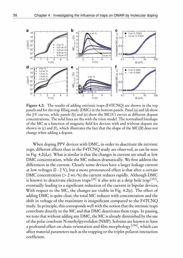
58 Chapter 4 : Investigating the influence of traps on OMAR by molecular doping
a b c
d e f
Figure 4.2: The results of adding extrinsic traps (F4TCNQ) are shown in the toppanels and for the trap filling study (DMC) in the bottom panels. Panel (a) and (d) showthe J-V curves, while panels (b) and (e) show the MC(V ) curves at different dopantconcentrations. The solid lines are fits with the trion model. The normalised lineshapeof the MC as a function of magnetic field for devices with and without dopant areshown in (c) and (f), which illustrates the fact that the shape of the MC(B) does notchange when adding a dopant.
When doping PPV devices with DMC, in order to deactivate the intrinsictraps, different effects than in the F4TCNQ study are observed, as can be seenin Fig. 4.2(d,e). What is similar is that the changes in current are small at lowDMC concentration, while the MC reduces dramatically. We first address thedifferences in the current. Clearly some devices have a larger leakage currentat low voltages (0 - 2 V), but a more pronounced effect is that after a certainDMC concentration (> 2 wt.-%) the current reduces rapidly. Although DMCis known to deactivate electron traps[24] it also acts as a deep hole trap[153],eventually leading to a significant reduction of the current in bipolar devices.With respect to the MC, the changes are visible in Fig. 4.2(e). The effect ofadding DMC is quite clear, the total MC reduces with concentration and theshift in voltage of the maximum is insignificant compared to the F4TCNQstudy. In principle, this corresponds well with the notion that the intrinsic trapscontribute directly to the MC and that DMC deactivates these traps. In passing,we note that without adding any DMC, the MC is already diminished by the useof the polar cosolvent N-methylpyrrolidon (NMP). Solvents are known to havea profound effect on chain orientation and film morphology[154], which canaffect material parameters such as the trapping or the triplet-polaron interactioncoefficient.
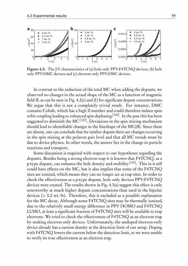
4.2 Experimental results 59
a b c
Figure 4.3: The J-V characteristics of (a) hole only PPV:F4TCNQ devices, (b) holeonly PPV:DMC devices and (c) electron only PPV:DMC devices.
In contrast to the reduction of the total MC when adding the dopants, weobserved no changes in the actual shape of the MC as a function of magneticfield B, as can be seen in Fig. 4.2(c) and (f) for significant dopant concentrations.We argue that this is not a completely trivial result. For instance, DMCcontains Cobalt, which has a high Z-number and could therefore induce spin-orbit coupling leading to enhanced spin dephasing [140]. In the past this has beensuggested to diminish the MC[122]. Deviations in the spin mixing mechanismshould lead to identifiable changes in the lineshape of the MC(B). Since theseare absent, one can conclude that for neither dopant there are changes occurringin the spin mixing at the polaron pair level and that all MC trends must bedue to device physics. In other words, the answer lies in the change in particlereactions and transport.
Some discussion is required with respect to our hypotheses regarding thedopants. Besides being a strong electron trap it is known that F4TCNQ, as ap-type dopant, can enhance the hole density and mobility[155]. This in it selfcould have effects on the MC, but it also implies that some of the F4TCNQsites are ionized, which means they can no longer act as trap sites. In order tocheck the effectiveness as a p-type dopant, hole only devices PPV:F4TCNQdevices were created. The results shown in Fig. 4.3(a) suggest this effect is onlynoteworthy at much higher dopant concentrations than used in the bipolardevices (> 0.2 wt.-%). Therefore, this is excluded as a possible explanationfor the MC decay. Although some F4TCNQ sites may be thermally ionized,due to the relatively small energy difference in PPV HOMO and F4TCNQLUMO, at least a significant fraction of F4TCNQ sites will be available to trapelectrons. We tried to check the effectiveness of F4TCNQ as an electron trapby making electron-only devices. Unfortunately, the undoped electron-onlydevice already has a current density at the detection limit of our setup. Dopingwith F4TCNQ lowers the current below the detection limit, so we were unableto verify its true effectiveness as an electron trap.
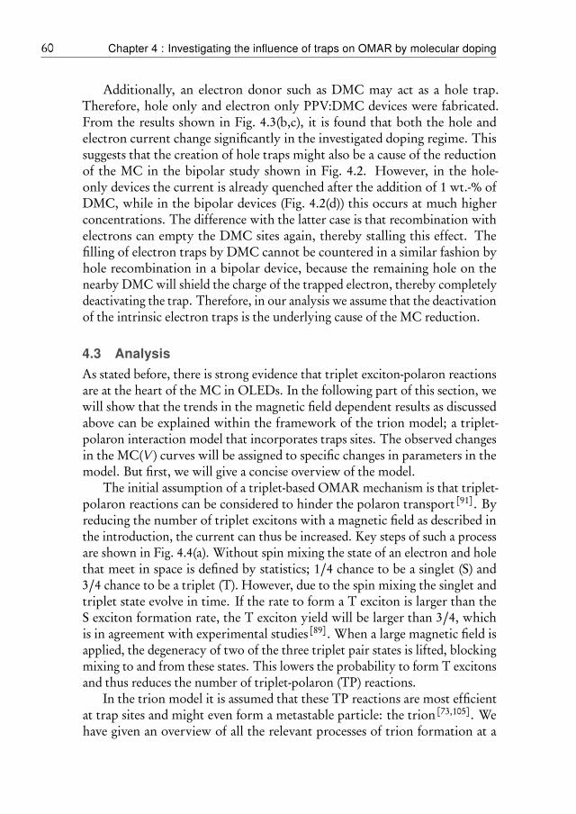
60 Chapter 4 : Investigating the influence of traps on OMAR by molecular doping
Additionally, an electron donor such as DMC may act as a hole trap.Therefore, hole only and electron only PPV:DMC devices were fabricated.From the results shown in Fig. 4.3(b,c), it is found that both the hole andelectron current change significantly in the investigated doping regime. Thissuggests that the creation of hole traps might also be a cause of the reductionof the MC in the bipolar study shown in Fig. 4.2. However, in the hole-only devices the current is already quenched after the addition of 1 wt.-% ofDMC, while in the bipolar devices (Fig. 4.2(d)) this occurs at much higherconcentrations. The difference with the latter case is that recombination withelectrons can empty the DMC sites again, thereby stalling this effect. Thefilling of electron traps by DMC cannot be countered in a similar fashion byhole recombination in a bipolar device, because the remaining hole on thenearby DMC will shield the charge of the trapped electron, thereby completelydeactivating the trap. Therefore, in our analysis we assume that the deactivationof the intrinsic electron traps is the underlying cause of the MC reduction.
4.3 Analysis
As stated before, there is strong evidence that triplet exciton-polaron reactionsare at the heart of the MC in OLEDs. In the following part of this section, wewill show that the trends in the magnetic field dependent results as discussedabove can be explained within the framework of the trion model; a triplet-polaron interaction model that incorporates traps sites. The observed changesin the MC(V ) curves will be assigned to specific changes in parameters in themodel. But first, we will give a concise overview of the model.
The initial assumption of a triplet-based OMAR mechanism is that triplet-polaron reactions can be considered to hinder the polaron transport[91]. Byreducing the number of triplet excitons with a magnetic field as described inthe introduction, the current can thus be increased. Key steps of such a processare shown in Fig. 4.4(a). Without spin mixing the state of an electron and holethat meet in space is defined by statistics; 1/4 chance to be a singlet (S) and3/4 chance to be a triplet (T). However, due to the spin mixing the singlet andtriplet state evolve in time. If the rate to form a T exciton is larger than theS exciton formation rate, the T exciton yield will be larger than 3/4, whichis in agreement with experimental studies[89]. When a large magnetic field isapplied, the degeneracy of two of the three triplet pair states is lifted, blockingmixing to and from these states. This lowers the probability to form T excitonsand thus reduces the number of triplet-polaron (TP) reactions.
In the trion model it is assumed that these TP reactions are most efficientat trap sites and might even form a metastable particle: the trion[73,105]. Wehave given an overview of all the relevant processes of trion formation at a
4.3 Analysis 61
γt
PTγR
(1-PT)γR
γTP
ktrion
kT
a
b
polaron pair
T exciton
S exciton
TP reaction
S0 state
Figure 4.4: (a) The process of spin mixing makes the pair’s spin state evolve intime from singlet to triplet. This means the probability to either form a singlet (S)or triplet (T) exciton is no longer only based on spin statistics, but also on theirseparate formation rates. When a large magnetic field is applied, the degeneracy oftwo of the three triplet pair states is lifted, blocking mixing to and from these states.This can reduce the probability to form T excitons and thus reduce the number oftriplet-polaron (TP) reactions. The TP reactions are the dominant exciton-polaroninteraction as T excitons live much longer than S excitons before recombining to theground state. (b) In our trion model we use this notion by assuming that electronswhich are trapped (with a coefficient γt) and recombine with holes (with a coefficientγR ) have a magnetic field dependent probability to form a triplet exciton (PT). Singletexcitons are neglected due to their short lifetime. The triplets can then recombinedirectly to the ground state with a rate kT or form a trion (with a coefficient γTP) byinteracting with another polaron. This trion can recombine again while releasing afree polaron with a rate ktrion. A magnetic field can thus reduce the number of tripletexcitons, leading to less trions and more free polarons.
trap site in Fig. 4.4, which are explained in more detail in the previous chapter.The model describes a cascade of particle reactions, starting at the trapping ofelectrons. These trapped electrons can react with free holes to form (triplet)excitons at the trap sites, which subsequently react with other free polarons toform trions. Trions can be argued to have a long lifetime, thereby significantlyaffecting the charge transport as polarons are temporarily captured by themuntil they recombine or dissociate. Such a trion model is able to describe theMC(V ) with an analytical fit function (see Fig. 4.1(d)). The initial increase of
62 Chapter 4 : Investigating the influence of traps on OMAR by molecular doping
MC as a function of V is due to the progressive formation of excitations (Texcitons and trions) from trapped electrons, while the subsequent decline iscaused by filling of the traps by these excitations.
We now apply this knowledge to analyse our experimental data. For theF4TCNQ study we observed that creating deep electron traps in PPV by addinga strong electron acceptor reduces and shifts the MC(V ). We conjectured thatthis happens because the intrinsic PPV trap sites have to compete for the freeelectrons with the F4TCNQ molecules. It can be argued that an exciton ortrion can only form on an intrinsic trap and not on F4TCNQ, where only aloosely bound charge transfer state can be formed with a hole in PPV. Thismeans the number of trions reduces through an effective reduction of theintrinsic trapping (because the electron trapping shifts to the F4TCNQ). Thetrion model then allows to assign the change in MC to the reduction of a singleparameter: the trapping coefficient γt of the electrons at the trap sites. All fitsin Fig. 4.2(b) can be attained by only varying this parameter, including theshift of the maximum MC to higher voltages. Due to the competition withF4TCNQ, one can take an effective trapping coefficient γt,eff from γt by takinga weighted average of γt and the dopant trapping coefficient γdop as:
γt,eff = γtγtNt
γtNt + γdopNdop, (4.1)
in which it is naturally assumed that the number of dopant sites Ndop scaleslinearly with the F4TCNQ concentration. As can be seen in Fig. 4.5(a) theeffective trapping coefficient taken from the fits indeed follows this trend.
We now turn to the DMC study. The reduction of the MC(V ) with DMCobserved in Fig. 4.2(e) can in principle be explained with the deactivation ofthe intrinsic electron traps. We find that the MC actually reduces linearly withDMC concentration. This can be expected from the trion model, since theMC scales linearly with the number of traps available for trion formation[73].Therefore, the MC(V ) is fitted with a varying trap site density Nt, although wealso had to allow the voltage dependence of the polaron density parameter a tochange slightly as well. As can be seen in Fig. 4.5(b) the effective trap densitytaken from the fits indeed follows this linear trend. At some concentrationall the electron traps will be filled and the MC reduces to zero. We note thatdifferent batches of devices created on separate days show a slightly differentdecline of the MC with DMC concentration. This could be due to the lowsolubility of DMC, leading to deviations in the concentrations. However, thetrend is always the same among devices created from the same solvent batch.
Not only does this study show that traps do indeed play a major role inthese magnetic field effects, more generally, it shows that molecular doping
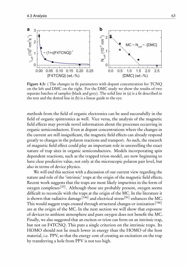
4.3 Analysis 63
a b
Figure 4.5: ( The changes in fit parameters with dopant concentration for TCNQon the left and DMC on the right. For the DMC study we show the results of twoseparate batches of samples (black and grey). The solid line in (a) is a fit described inthe text and the dotted line in (b) is a linear guide to the eye.
methods from the field of organic electronics can be used successfully in thefield of organic spintronics as well. Vice versa, the analysis of the magneticfield effects may provide novel information about the processes occurring inorganic semiconductors. Even at dopant concentrations where the changes inthe current are still insignificant, the magnetic field effects can already respondgreatly to changes in the polaron reactions and transport. As such, the researchof magnetic field effect could play an important role in unravelling the exactnature of trap sites in organic semiconductors. Models incorporating spindependent reactions, such as the trapped trion model, are now beginning tohave clear predictive value, not only at the microscopic polaron pair level, butalso in terms of device physics.
We will end this section with a discussion of our current view regarding thenature and role of the ‘intrinsic’ traps at the origin of the magnetic field effects.Recent work suggests that the traps are most likely impurities in the form ofoxygen complexes[23]. Although these are probably present, oxygen seemsdifficult to reconcile with the traps at the origin of the MC. In the literature itis shown that radiative damage[146] and electrical stress[81] enhances the MC.This would suggest traps created through structural changes or ionization [156]
are at the origin of the MC. In the next section we will show that exposureof devices to ambient atmosphere and pure oxygen does not benefit the MC.Finally, we also suggested that an exciton or trion can form on an intrinsic trap,but not on F4TCNQ. This puts a single criterion on the intrinsic traps. ItsHOMO should not lie much lower in energy than the HOMO of the hostmaterial, i.e. PPV, so that the energy cost of creating an excitation on the trapby transferring a hole from PPV is not too high.
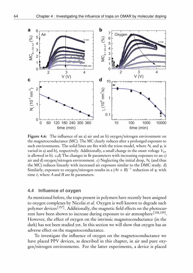
64 Chapter 4 : Investigating the influence of traps on OMAR by molecular doping
a b
c d
Figure 4.6: The influence of an a) air and an b) oxygen/nitrogen environment onthe magnetoconductance (MC). The MC clearly reduces after a prolonged exposure tosuch environments. The solid lines are fits with the trion model, where Nt and γt isvaried in a) and b), respectively. Additionally, a small change in the onset voltage Vonis allowed in b). c,d) The changes in fit parameters with increasing exposure to an c)air and d) oxygen/nitrogen environment. c) Neglecting the initial drop, Nt (and thusthe MC) reduces linearly with increased air exposure similar to the DMC study. d)Similarly, exposure to oxygen/nitrogen results in a (At + B)−1 reduction of γt withtime t, where A and B are fit parameters.
4.4 Influence of oxygen
As mentioned before, the traps present in polymers have recently been assignedto oxygen complexes by Nicolai et al. Oxygen is well known to degrade suchpolymer devices[157]. Additionally, the magnetic field effects on the photocur-rent have been shown to increase during exposure to air atmosphere[158,159].However, the effect of oxygen on the intrinsic magnetoconductance (in thedark) has not been studied yet. In this section we will show that oxygen has anadverse effect on the magnetoconductance.
To investigate the influence of oxygen on the magnetoconductance wehave placed PPV devices, as described in this chapter, in air and pure oxy-gen/nitrogen environments. For the latter experiments, a device is placed
4.5 Conclusion 65
inside a concealed chamber which is connect to a Turbomolecular VacuumPumping System (Varian, model minitask AG81). Air is first pumped out,after which it is filled with nitrogen, then the device is placed inside and thechamber is filled with the oxygen/nitrogen mixture. After each controlledexposure to either environment the devices are placed back into the nitrogenfilled glovebox where they are electrically characterized. This means the devicesare never actually operated in an oxygen environment. The results of this studyare shown in Fig. 4.6.
For both environments the MC reduces significantly with increasing expo-sure times. However, a pronounced difference is observed in both trends, whichresembles the difference in the DMC/F4TCNQ study. In an air atmospherea total reduction of MC is observed without a shift in peak voltage, similarto doping with DMC. In a oxygen/nitrogen environment the MC also shiftsto higher voltages, similar to doping with F4TCNQ. Equivalently, the resultscan be fitted with the trion model in a similar manner as the DMC/F4TCNQstudy. This could indicate that oxygen acts as a strong electron acceptor likeF4TCNQ, while the degradation process in air deactivates the traps responsi-ble for the MC, or adds hole traps, similar to DMC. The difference betweenair and pure oxygen might be attributed to water vapor or other compoundspresent in air that react with the polymer device. In the air environment thedevices are also exposed to relatively more ambient light, which may lead tophoto-oxidation processes. Alternatively, molecular oxygen is known to diffuseinto polymer films and quench triplet excited states [160,161]. This additionaleffect may also reduce the magnetoresistance, most likely in a different mannerthan a photo-oxidation process.
Clearly, more work is required to elucidate the exact cause of the differenttrends. We do conclude that oxygen and air atmosphere have a detrimentaleffect on the MC, which suggests traps induced by these compounds are not atthe origin of the MC.
4.5 Conclusion
In conclusion, using well known dopants we have investigated the influence oftraps on magnetic field effects in the semiconducting polymer ’super yellow’PPV. We used the strong electron acceptor F4TCNQ and found that themagnetoconductance (MC) declines rapidly with F4TCNQ concentration in amanner that can be assigned to a reduction in the effective electron trappingat the intrinsic trap sites. This result shows that while the intrinsic electrontraps of PPV lead to a large MC, the traps induced by the dopant do not, andcompetition of the latter with the intrinsic traps leads to an eventual decline.Additionally, we used the electron donor DMC that is known to fill and
66 Chapter 4 : Investigating the influence of traps on OMAR by molecular doping
deactivate the PPV traps. This latter study showed a linear decline of the MCas the traps become filled, although we cannot entirely exclude that creatinghole traps has no similar effect. Both studies clearly indicate that traps play acrucial role in the large MC observed in thin film PPV devices. Oxygen andair also seem to have an adverse effect on MC, which suggests traps induced bythese compounds are not at the origin of the MC. Not only are these resultshighly relevant for the fundamental understanding of spin physics and magneticfield effects in organic semiconductors, they also suggest that traps—which aregenerally considered detrimental for device performance—can be beneficiallyutilized in organic magnetic field sensors.
5Spectroscopic evidence fortrap-dominated magnetic fieldeffects in organicsemiconductors
Polaron traps are ubiquitous in organic semiconductors and recent evidence sug-gests they might be crucial for the large observed magnetic field effects (MFEs) inorganic semiconductors. Here we measure MFEs in polymer thin film devices withengineered, radiative trap sites in order to spectroscopically investigate the influenceof the traps. Surprisingly, the luminescence at the trap sites and the polymer back-bone is found to have an opposite response to a magnetic field. All our results arecompatible with a novel mechanism, in which spin mixing at the traps can createthe large MFEs observed on the backbone. This scenario is quantitatively confirmedby numerical drift-diffusion modelling with magnetic field dependent excitondensities at the traps. These insights solve an outstanding controversy within theresearch field.
Published as: M. Cox et al., Physical Review B 90, 155205 (2014).
67
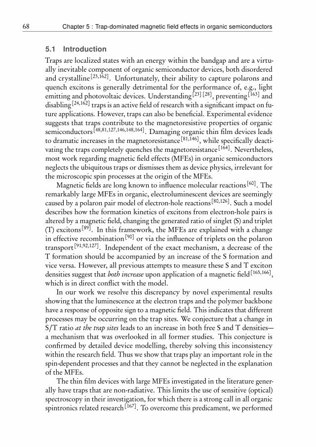
68 Chapter 5 : Trap-dominated magnetic field effects in organic semiconductors
5.1 Introduction
Traps are localized states with an energy within the bandgap and are a virtu-ally inevitable component of organic semiconductor devices, both disorderedand crystalline[23,162]. Unfortunately, their ability to capture polarons andquench excitons is generally detrimental for the performance of, e.g., lightemitting and photovoltaic devices. Understanding [23] [28], preventing[163] anddisabling[24,162] traps is an active field of research with a significant impact on fu-ture applications. However, traps can also be beneficial. Experimental evidencesuggests that traps contribute to the magnetoresistive properties of organicsemiconductors[48,81,127,146,148,164]. Damaging organic thin film devices leadsto dramatic increases in the magnetoresistance[81,146], while specifically deacti-vating the traps completely quenches the magnetoresistance[164]. Nevertheless,most work regarding magnetic field effects (MFEs) in organic semiconductorsneglects the ubiquitous traps or dismisses them as device physics, irrelevant forthe microscopic spin processes at the origin of the MFEs.
Magnetic fields are long known to influence molecular reactions[60]. Theremarkably large MFEs in organic, electroluminescent devices are seeminglycaused by a polaron pair model of electron-hole reactions[80,126]. Such a modeldescribes how the formation kinetics of excitons from electron-hole pairs isaltered by a magnetic field, changing the generated ratio of singlet (S) and triplet(T) excitons[89]. In this framework, the MFEs are explained with a changein effective recombination[90] or via the influence of triplets on the polarontransport[91,92,127]. Independent of the exact mechanism, a decrease of theT formation should be accompanied by an increase of the S formation andvice versa. However, all previous attempts to measure these S and T excitondensities suggest that both increase upon application of a magnetic field[165,166],which is in direct conflict with the model.
In our work we resolve this discrepancy by novel experimental resultsshowing that the luminescence at the electron traps and the polymer backbonehave a response of opposite sign to a magnetic field. This indicates that differentprocesses may be occurring on the trap sites. We conjecture that a change inS/T ratio at the trap sites leads to an increase in both free S and T densities—a mechanism that was overlooked in all former studies. This conjecture isconfirmed by detailed device modelling, thereby solving this inconsistencywithin the research field. Thus we show that traps play an important role in thespin-dependent processes and that they cannot be neglected in the explanationof the MFEs.
The thin film devices with large MFEs investigated in the literature gener-ally have traps that are non-radiative. This limits the use of sensitive (optical)spectroscopy in their investigation, for which there is a strong call in all organicspintronics related research[167]. To overcome this predicament, we performed
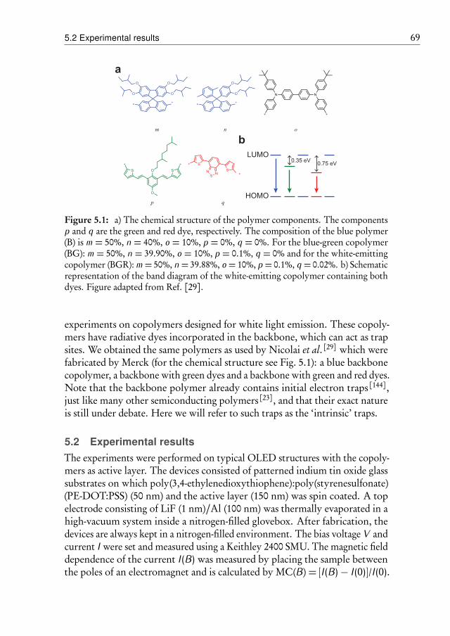
5.2 Experimental results 69
a
LUMO
HOMO
0.35 eV
b
0.75 eV
Figure 5.1: a) The chemical structure of the polymer components. The componentsp and q are the green and red dye, respectively. The composition of the blue polymer(B) is m = 50%, n = 40%, o = 10%, p = 0%, q = 0%. For the blue-green copolymer(BG): m = 50%, n = 39.90%, o = 10%, p = 0.1%, q = 0% and for the white-emittingcopolymer (BGR):m= 50%, n= 39.88%, o= 10%, p= 0.1%, q= 0.02%. b) Schematicrepresentation of the band diagram of the white-emitting copolymer containing bothdyes. Figure adapted from Ref. [29].
experiments on copolymers designed for white light emission. These copoly-mers have radiative dyes incorporated in the backbone, which can act as trapsites. We obtained the same polymers as used by Nicolai et al.[29] which werefabricated by Merck (for the chemical structure see Fig. 5.1): a blue backbonecopolymer, a backbone with green dyes and a backbone with green and red dyes.Note that the backbone polymer already contains initial electron traps[144],just like many other semiconducting polymers[23], and that their exact natureis still under debate. Here we will refer to such traps as the ‘intrinsic’ traps.
5.2 Experimental results
The experiments were performed on typical OLED structures with the copoly-mers as active layer. The devices consisted of patterned indium tin oxide glasssubstrates on which poly(3,4-ethylenedioxythiophene):poly(styrenesulfonate)(PE-DOT:PSS) (50 nm) and the active layer (150 nm) was spin coated. A topelectrode consisting of LiF (1 nm)/Al (100 nm) was thermally evaporated in ahigh-vacuum system inside a nitrogen-filled glovebox. After fabrication, thedevices are always kept in a nitrogen-filled environment. The bias voltage V andcurrent I were set and measured using a Keithley 2400 SMU. The magnetic fielddependence of the current I(B) was measured by placing the sample betweenthe poles of an electromagnet and is calculated by MC(B) = [I(B)− I(0)]/I(0).
70 Chapter 5 : Trap-dominated magnetic field effects in organic semiconductors
400 500 600 700 8000
1
400 500 600 700 800-202468
1012
3 4 50.0
0.1
0.2
2.5 3.0 3.5 4.0 4.5 5.0-202468
1012
5 V
2.8 V stressed
Nor
mal
ized
EL
(nm)
2.8 V
a
~0.8 eV
c
ME
L (%
)
(nm)
5 V
2.8 V stressed
2.8 V
c)
b
EL 64
0 nm
/EL 46
0 nm
stressing
V (V)
ME
L (%
)
d
V (V)
stressing
Figure 5.2: Electroluminescence (EL) and magneto-electroluminescence (MEL)measurements performed on the blue light emitting polymer. a) The normalized ELas a function of wavelength for a pristine device at currents corresponding to 2.8 Vand 5 V and a stressed device at 2.8 V. Two peaks are observed: one for bimolecularrecombination at 460 nm and one for trap-assisted recombination at 640 nm. b) Therelative ratio of the EL at 640 nm with respect to 460 nm as a function of voltageand different amounts of electrical stressing. Results are shown for a pristine device(squares), after stressing at 6.5 V (circles) and after stressing at 7.5 V (triangles). Thedata points along the arrow were measured at the same current to show the increasedratio is not solely due to a voltage shift. Power law fits are used as a guide to the eye(lines). c) The MEL at a fixed magnetic field of 10 mT as a function of wavelengthfor the same conditions as shown in a). d) The MEL at 460 nm (open symbols) and700 nm (closed symbols) as a function of voltage and electrical stress with the sameconditions as shown in b).
The electroluminescence EL was measured with a silicon photodiode or with aspectrometer, which consisted of a spectrograph (Newport MS260i) and back-illuminated CCD (Andor DV420-BV). EL measurements with the spectrometerare performed at constant currents.
5.2 Experimental results 71
Backbone polymer
We first turn the attention to the results of the blue backbone polymer, forwhich the electroluminescence (EL) and magneto-electroluminescence (MEL)results are shown in Fig. 5.2. The EL spectrum shown in Fig. 1a shows aclear peak around 450 nm, consistent with bimolecular recombination at thebackbone. Surprisingly, at low voltages luminescence is also visible at muchlonger wavelengths. This luminescence seems to peak around 640 nm and itdoes not increase as rapidly with voltage as the backbone emission. The relativereduction of this light emission with respect to the backbone emission, shownin Fig. 5.2b, is a clear signature of deep trap-assisted Shockley-Read-Hall (SRH)recombination[28]. Trap-assisted recombination is basically a monomolecularprocess, which scales weaker with increasing charge density (and thus increasingvoltage) than a bimolecular process occurring on the backbone. The relativelylarge energy difference between the bimolecular and trap-assisted emission (∼0.8 eV) indicates the traps are positioned deep within the bandgap.
The new observation that the initial or ‘intrinsic’ traps are radiative makesit possible to investigate the magnetic field effects occurring on and due tothese traps. Results of the spectrally resolved MEL are shown in Fig. 5.2c. Asexpected, the EL around 450 nm increases significantly when a magnetic fieldis applied. More interestingly, we find a sign change of the MEL at wavelengthsthat correspond to the trap-assisted recombination. Additionally, it is observedthat the bimolecular backbone MEL reduces strongly with voltage (shownin Fig. 5.2d), while the reduction of the trap-assisted MEL seems to be lessstrong or absent. Note that at higher voltage the EL around 640 nm is mainlydominated by the shoulder of the bimolecular recombination (see Fig. 5.2a).This may affect the observed weak voltage dependence of the trap-assistedMEL.
To investigate the influence of these traps more closely, electrical stressingexperiments were performed. Electrical stress has been shown to enhancethe MFEs, which was suggested to be due to the formation of trap sites[81].Here, two experiments were performed in sequence, first a voltage of 6.5 Vwas applied for one hour and subsequently a voltage of 7.5 V for one hour.After each run MC, EL and MEL were measured. The MC was found toincrease after each run (not shown here), similar to what was observed inthe literature. Because the traps are radiative, we now have access to therelative contribution of the trap-assisted recombination increases with electricalstressing, as can be seen in the EL of Fig. 5.2a,b. These results further strengthenthe notion that the contribution of traps enhances after device degradation.Furthermore, in Fig. 5.2c,d it is observed that the MEL arising from thebimolecular recombination increases with electrical stressing, however, theMEL from the trap-assisted recombination remains approximately constant.
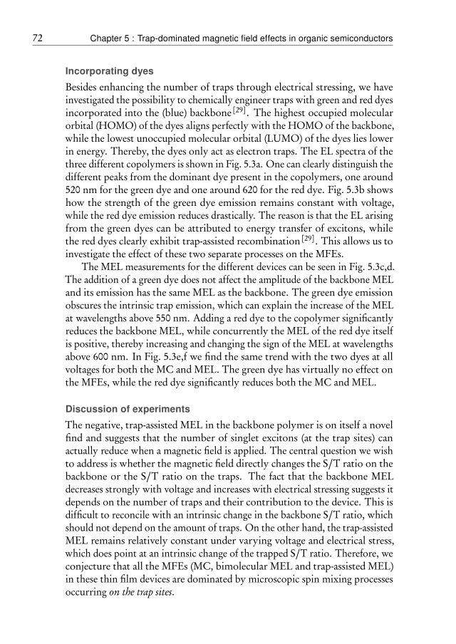
72 Chapter 5 : Trap-dominated magnetic field effects in organic semiconductors
Incorporating dyes
Besides enhancing the number of traps through electrical stressing, we haveinvestigated the possibility to chemically engineer traps with green and red dyesincorporated into the (blue) backbone[29]. The highest occupied molecularorbital (HOMO) of the dyes aligns perfectly with the HOMO of the backbone,while the lowest unoccupied molecular orbital (LUMO) of the dyes lies lowerin energy. Thereby, the dyes only act as electron traps. The EL spectra of thethree different copolymers is shown in Fig. 5.3a. One can clearly distinguish thedifferent peaks from the dominant dye present in the copolymers, one around520 nm for the green dye and one around 620 for the red dye. Fig. 5.3b showshow the strength of the green dye emission remains constant with voltage,while the red dye emission reduces drastically. The reason is that the EL arisingfrom the green dyes can be attributed to energy transfer of excitons, whilethe red dyes clearly exhibit trap-assisted recombination [29]. This allows us toinvestigate the effect of these two separate processes on the MFEs.
The MEL measurements for the different devices can be seen in Fig. 5.3c,d.The addition of a green dye does not affect the amplitude of the backbone MELand its emission has the same MEL as the backbone. The green dye emissionobscures the intrinsic trap emission, which can explain the increase of the MELat wavelengths above 550 nm. Adding a red dye to the copolymer significantlyreduces the backbone MEL, while concurrently the MEL of the red dye itselfis positive, thereby increasing and changing the sign of the MEL at wavelengthsabove 600 nm. In Fig. 5.3e,f we find the same trend with the two dyes at allvoltages for both the MC and MEL. The green dye has virtually no effect onthe MFEs, while the red dye significantly reduces both the MC and MEL.
Discussion of experiments
The negative, trap-assisted MEL in the backbone polymer is on itself a novelfind and suggests that the number of singlet excitons (at the trap sites) canactually reduce when a magnetic field is applied. The central question we wishto address is whether the magnetic field directly changes the S/T ratio on thebackbone or the S/T ratio on the traps. The fact that the backbone MELdecreases strongly with voltage and increases with electrical stressing suggests itdepends on the number of traps and their contribution to the device. This isdifficult to reconcile with an intrinsic change in the backbone S/T ratio, whichshould not depend on the amount of traps. On the other hand, the trap-assistedMEL remains relatively constant under varying voltage and electrical stress,which does point at an intrinsic change of the trapped S/T ratio. Therefore, weconjecture that all the MFEs (MC, bimolecular MEL and trap-assisted MEL)in these thin film devices are dominated by microscopic spin mixing processesoccurring on the trap sites.
5.2 Experimental results 73
a b
c d
e f
Figure 5.3: Electroluminescence (EL), magneto-electroluminescence (MEL) andmagneto-conductance (MC) measurements for the blue backbone copolymer (B), thecopolymer with green dyes (BG) and the copolymer with green and red dyes (BGR).In a) the normalized EL of the three different devices is shown at 2.8 V. b) The red dyeemission (640 nm) in the BGR polymer shows a strong voltage dependence w.r.t. thebackbone emission, while the green dye emission (520 nm) does not. In c) the MELof the devices is shown at 2.8 V. d) EL spectra for the BGR device with varying biasvoltage. In e) and f) the MC and MEL are shown as a function of voltage. Note that theMEL in c) and d) was measured at constant current, while the MEL in e) was measuredat constant voltage as it was measured with a photodiode together with the MC. TheMC and MEL are shown for a fixed magnetic field strength of approximately 10 mT.

74 Chapter 5 : Trap-dominated magnetic field effects in organic semiconductors
HOMO
LUMO
trap
i)
ii)
iii)
Figure 5.4: Schematic overview of the possible spin-selective steps in a trap-assistedrecombination process. i) The electron trapping itself can be spin selective, resultingin a magnetic field dependent trapping rate. ii) Competition between electron-holerecombination and dissociation can be spin selective, resulting in a magnetic fielddependent (effective) recombination rate. iii) Spin-selective recombination of electron-hole precursor pairs can result in a magnetic field dependent singlet/triplet excitonratio.
The experimental results from the BG and BGR polymers suggest thatcapturing excitons generated from bimolecular recombination with the greendyes has no effect on the MFEs, while adding electron traps with the reddyes can significantly alter the MFEs. These results correspond again withthe conjecture that traps are at the origin of the MFEs and not the processesoccurring on the backbone. While electrical stressing enhances the MFEs bycreating additional traps with the same magnetic response, the red dyes have anopposite MEL compared to the intrinsic traps, which results in a reduction ofthe total MC and backbone MEL. These results indicate that the exact physicalorigin of the traps has a drastic influence on both the strength and sign of theMFEs.
5.3 Numerical calculations
Our experimental results suggest that a change in recombination at trap sitescan lead to an opposite response in the bimolecular recombination and current.Previously, it was assumed that the S/T exciton ratio should change in favourof the singlets on application of B to explain a positive MEL [89]. Now wefind the opposite in our experimental results regarding the blue copolymer: anegative trap-assisted MEL indicates a reduction of the S exciton density at thetraps with B, which suggests an increase of T excitons (at the traps). But howcan this cause the observed MFEs at the backbone?
To answer this question we investigated multiple spin-dependent mech-anisms at the traps. As illustrated in Fig. 5.4, trap-assisted recombination
5.3 Numerical calculations 75
consists of multiple steps that could be spin selective. These steps includeelectron trapping, electron-hole recombination and exciton formation. Withinthe framework of a polaron pair model, a magnetic field can influence any ofthese processes. Magnetic field dependent trapping could arise if the groundstate of the trap site is a spin radical, such as an oxygen complex. The trap itselfwould then act as the second particle in a pair. Similar to electron-hole recom-bination in a bimolecular reaction, a magnetic field can influence the effectiverecombination rate[90] or the formed singlet/triplet exciton ratio [89]. We notethat unlike excitons created in a bimolecular process on the backbone, whichare free to move around, the excitons created in a trap-assisted recombinationprocess will most likely occupy the trap on which they were formed.
These mechanisms are investigated quantitatively with a drift-diffusiondevice model, where the magnetic field effect is incorporated as a change ina material parameter[73], such as the trapping coefficient. We recently ex-ploited such an approach to describe magnetic field effects in polymer-fullereneblends[80] and electrochemical cells[149]. This device model can easily incorpo-rate bimolecular Langevin recombination, trap-assisted SRH recombinationand exciton formation.
The model includes free holes and electrons with a density p and n re-spectively and mobility µ. Free electrons are trapped with a coefficient Cnat the available trap sites density Nt, resulting in a trapped electron densitynt. For simplicity we implemented deep electron traps with a single energylevel Et below the LUMO. Electron trapping only occurs if a trap is empty.The trapping rate thus depends not only on the number of traps Nt but alsoon their occupation f = (nt + Tt)/Nt, which includes the trapped electrondensity Nt and the (optional) trapped exciton density Tt. Trapped electronsand free holes undergo trap-assisted recombination with a coefficient Cp. Inthe case of exciton formation, triplet excitons are formed from this processwith a magnetic field dependent probability PT(B). We neglect the singletexciton density because of their short lifetime. The triplets will undergo amonomolecular decay governed by their lifetime τT.
Most material parameters are taken from the device characterisation ofNicolai et al.[29,144]. The LUMO and HOMO energy are 2.2 eV and 5.3 eV,respectively. We used µ = 10−10 m2V−1s−1, Et = 0.8 eV and Cn = Cp =9 × 10⁻¹⁹ m3s−1. Triplet lifetimes can be taken from the literature[168,169].Monomolecular decay rates of more than 0.5 ms have been found for free tripletexcitons [168], while at trap sites triplets have been suggested to live longer than100 ms at ambient temperature[169]. Here we take a triplet lifetime of τT = 5ms, which still results in significant trap-occupation yet manageable calculationtimes.
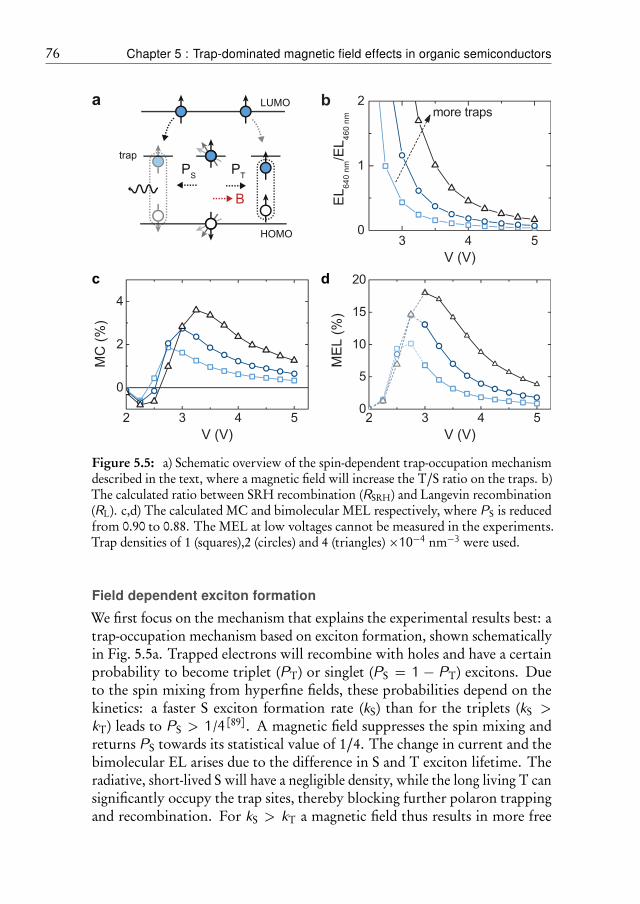
76 Chapter 5 : Trap-dominated magnetic field effects in organic semiconductors
HOMO
LUMO
trap
a
PT
PS
B
Figure 5.5: a) Schematic overview of the spin-dependent trap-occupation mechanismdescribed in the text, where a magnetic field will increase the T/S ratio on the traps. b)The calculated ratio between SRH recombination (RSRH) and Langevin recombination(RL). c,d) The calculated MC and bimolecular MEL respectively, where PS is reducedfrom 0.90 to 0.88. The MEL at low voltages cannot be measured in the experiments.Trap densities of 1 (squares),2 (circles) and 4 (triangles) ×10−4 nm−3 were used.
Field dependent exciton formation
We first focus on the mechanism that explains the experimental results best: atrap-occupation mechanism based on exciton formation, shown schematicallyin Fig. 5.5a. Trapped electrons will recombine with holes and have a certainprobability to become triplet (PT) or singlet (PS = 1 − PT) excitons. Dueto the spin mixing from hyperfine fields, these probabilities depend on thekinetics: a faster S exciton formation rate (kS) than for the triplets (kS >kT) leads to PS > 1/4[89]. A magnetic field suppresses the spin mixing andreturns PS towards its statistical value of 1/4. The change in current and thebimolecular EL arises due to the difference in S and T exciton lifetime. Theradiative, short-lived S will have a negligible density, while the long living T cansignificantly occupy the trap sites, thereby blocking further polaron trappingand recombination. For kS > kT a magnetic field thus results in more free
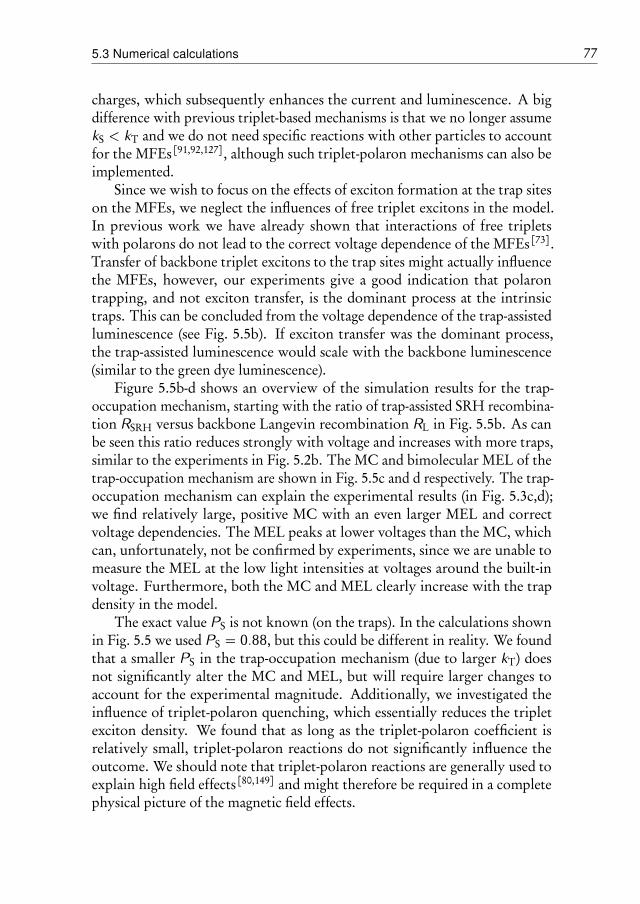
5.3 Numerical calculations 77
charges, which subsequently enhances the current and luminescence. A bigdifference with previous triplet-based mechanisms is that we no longer assumekS < kT and we do not need specific reactions with other particles to accountfor the MFEs[91,92,127], although such triplet-polaron mechanisms can also beimplemented.
Since we wish to focus on the effects of exciton formation at the trap siteson the MFEs, we neglect the influences of free triplet excitons in the model.In previous work we have already shown that interactions of free tripletswith polarons do not lead to the correct voltage dependence of the MFEs[73].Transfer of backbone triplet excitons to the trap sites might actually influencethe MFEs, however, our experiments give a good indication that polarontrapping, and not exciton transfer, is the dominant process at the intrinsictraps. This can be concluded from the voltage dependence of the trap-assistedluminescence (see Fig. 5.5b). If exciton transfer was the dominant process,the trap-assisted luminescence would scale with the backbone luminescence(similar to the green dye luminescence).
Figure 5.5b-d shows an overview of the simulation results for the trap-occupation mechanism, starting with the ratio of trap-assisted SRH recombina-tion RSRH versus backbone Langevin recombination RL in Fig. 5.5b. As canbe seen this ratio reduces strongly with voltage and increases with more traps,similar to the experiments in Fig. 5.2b. The MC and bimolecular MEL of thetrap-occupation mechanism are shown in Fig. 5.5c and d respectively. The trap-occupation mechanism can explain the experimental results (in Fig. 5.3c,d);we find relatively large, positive MC with an even larger MEL and correctvoltage dependencies. The MEL peaks at lower voltages than the MC, whichcan, unfortunately, not be confirmed by experiments, since we are unable tomeasure the MEL at the low light intensities at voltages around the built-involtage. Furthermore, both the MC and MEL clearly increase with the trapdensity in the model.
The exact value PS is not known (on the traps). In the calculations shownin Fig. 5.5 we used PS = 0.88, but this could be different in reality. We foundthat a smaller PS in the trap-occupation mechanism (due to larger kT) doesnot significantly alter the MC and MEL, but will require larger changes toaccount for the experimental magnitude. Additionally, we investigated theinfluence of triplet-polaron quenching, which essentially reduces the tripletexciton density. We found that as long as the triplet-polaron coefficient isrelatively small, triplet-polaron reactions do not significantly influence theoutcome. We should note that triplet-polaron reactions are generally used toexplain high field effects[80,149] and might therefore be required in a completephysical picture of the magnetic field effects.
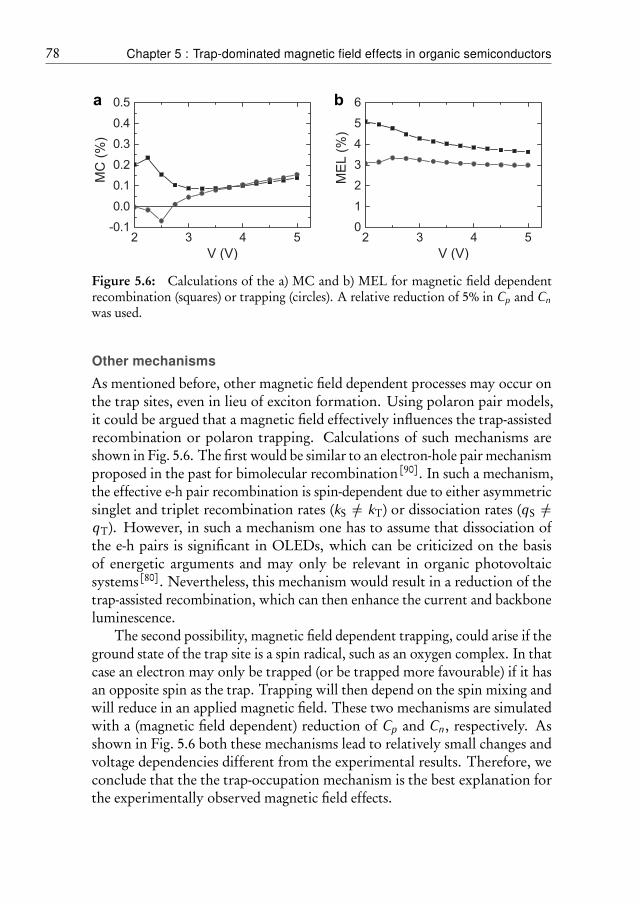
78 Chapter 5 : Trap-dominated magnetic field effects in organic semiconductors
a b
Figure 5.6: Calculations of the a) MC and b) MEL for magnetic field dependentrecombination (squares) or trapping (circles). A relative reduction of 5% in Cp and Cnwas used.
Other mechanisms
As mentioned before, other magnetic field dependent processes may occur onthe trap sites, even in lieu of exciton formation. Using polaron pair models,it could be argued that a magnetic field effectively influences the trap-assistedrecombination or polaron trapping. Calculations of such mechanisms areshown in Fig. 5.6. The first would be similar to an electron-hole pair mechanismproposed in the past for bimolecular recombination[90]. In such a mechanism,the effective e-h pair recombination is spin-dependent due to either asymmetricsinglet and triplet recombination rates (kS 6= kT) or dissociation rates (qS 6=qT). However, in such a mechanism one has to assume that dissociation ofthe e-h pairs is significant in OLEDs, which can be criticized on the basisof energetic arguments and may only be relevant in organic photovoltaicsystems[80]. Nevertheless, this mechanism would result in a reduction of thetrap-assisted recombination, which can then enhance the current and backboneluminescence.
The second possibility, magnetic field dependent trapping, could arise if theground state of the trap site is a spin radical, such as an oxygen complex. In thatcase an electron may only be trapped (or be trapped more favourable) if it hasan opposite spin as the trap. Trapping will then depend on the spin mixing andwill reduce in an applied magnetic field. These two mechanisms are simulatedwith a (magnetic field dependent) reduction of Cp and Cn, respectively. Asshown in Fig. 5.6 both these mechanisms lead to relatively small changes andvoltage dependencies different from the experimental results. Therefore, weconclude that the the trap-occupation mechanism is the best explanation forthe experimentally observed magnetic field effects.
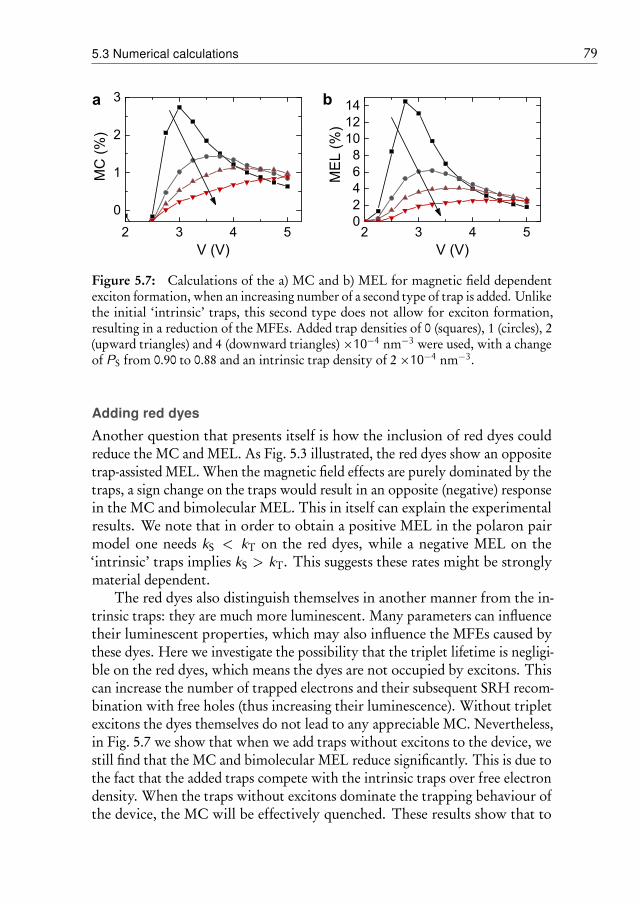
5.3 Numerical calculations 79
2 3 4 50
1
2
3
2 3 4 502468
101214a
MC
(%)
V (V)
ME
L (%
)
b
V (V)
Figure 5.7: Calculations of the a) MC and b) MEL for magnetic field dependentexciton formation, when an increasing number of a second type of trap is added. Unlikethe initial ‘intrinsic’ traps, this second type does not allow for exciton formation,resulting in a reduction of the MFEs. Added trap densities of 0 (squares), 1 (circles), 2(upward triangles) and 4 (downward triangles) ×10−4 nm−3 were used, with a changeof PS from 0.90 to 0.88 and an intrinsic trap density of 2 ×10⁻⁴ nm−3.
Adding red dyes
Another question that presents itself is how the inclusion of red dyes couldreduce the MC and MEL. As Fig. 5.3 illustrated, the red dyes show an oppositetrap-assisted MEL. When the magnetic field effects are purely dominated by thetraps, a sign change on the traps would result in an opposite (negative) responsein the MC and bimolecular MEL. This in itself can explain the experimentalresults. We note that in order to obtain a positive MEL in the polaron pairmodel one needs kS < kT on the red dyes, while a negative MEL on the‘intrinsic’ traps implies kS > kT. This suggests these rates might be stronglymaterial dependent.
The red dyes also distinguish themselves in another manner from the in-trinsic traps: they are much more luminescent. Many parameters can influencetheir luminescent properties, which may also influence the MFEs caused bythese dyes. Here we investigate the possibility that the triplet lifetime is negligi-ble on the red dyes, which means the dyes are not occupied by excitons. Thiscan increase the number of trapped electrons and their subsequent SRH recom-bination with free holes (thus increasing their luminescence). Without tripletexcitons the dyes themselves do not lead to any appreciable MC. Nevertheless,in Fig. 5.7 we show that when we add traps without excitons to the device, westill find that the MC and bimolecular MEL reduce significantly. This is due tothe fact that the added traps compete with the intrinsic traps over free electrondensity. When the traps without excitons dominate the trapping behaviour ofthe device, the MC will be effectively quenched. These results show that to
80 Chapter 5 : Trap-dominated magnetic field effects in organic semiconductors
engineer the magnetic field effects in devices one should thus always add trapswith favourable parameters, such as a long triplet exciton lifetime.
5.4 Implications and conclusion
The experimental and numerical results are crucial for the fundamental un-derstanding of magnetic field effects. A change in S/T ratio at the traps canenhance the current and backbone luminescence. An increase in both singletand triplet exciton densities, as was measured in the literature[165,166], thusoccurs simply because the total electron-hole recombination increases on thebackbone. What should be measured instead are the magnetic field dependentsinglet and triplet densities at the trap sites. Our experimental results providethe first verification that the singlet exciton density at the trap sites can indeeddecrease. Additionally, our results have implications for predictive OLEDmodels. We find that these should include long living excitations at the trapsites.
In conclusion, the magnetic field dependent current and luminescence inpolymer thin films with radiative traps was investigated spectroscopically. Sur-prisingly, we found an opposite response in the magneto-electroluminescence(MEL) of the traps with respect to the backbone. The magnetoconductance(MC) and MEL can be tuned by creating traps through electrical stressing orincorporation of dyes. The experimental results strongly suggest that magneticfield dependent processes at the trap sites affect the MC and MEL in the de-vice. Numerical device calculations further elucidated that a magnetic fielddependent triplet exciton density at the trap sites can explain the magneticfield effects. An increase in triplet excitons with magnetic field will lead to areduction in polaron trapping and recombination, which enhances the currentand backbone luminescence. These results show that trap sites and their in-fluence on devices cannot be neglected—and might in fact dominate—in theexplanation of magnetic field effects and the underlying spin physics in organicsemiconductors.
6Anisotropic magnetoconductancein polymer thin films
The dependence of the magnetic field sensitive current on the orientation of themagnetic field has been investigated in organic semiconductor devices where theactive layer consists of the poly(p-phenylene vinylene) derivative ’Super Yellow’. Pre-vious work on Alq3 suggested that the anisotropy was caused either by anisotropicspin-spin interactions or by anistropic hyperfine fields, but no discrimination couldbe made. In the present work, the anisotropy at the hyperfine field scale is bestexplained by dipolar coupling between the spin of polarons. In addition, a high fieldanisotropy is found with an opposite sign, different angle and voltage dependence.Spin density matrix calculations were performed of polaron pair interactions for thelow field effect, and a ∆g-mechanism, triplet-polaron or triplet-triplet interactionfor the high field effect. The simulations confirm that the low field anisotropy canindeed be explained by dipolar coupling. However, the proposed models can notentirely account for the high field anisotropy. These results show that, althoughcontemporary models can account for (anisotropic) magnetic field effects in organicsemiconductors at low field scales, more experimental and theoretical research ofhigh field effects is highly desirable.
Published as: M. Cox et al., Phys. Rev. B 89, 195204 (2014)
81
82 Chapter 6 : Anisotropic magnetoconductance in polymer thin films
6.1 Introduction
Large changes in the current and luminescence with magnetic field have beenobserved in organic semiconducting devices during the last decade. Such effectshave been investigated in organic light emitting devices (OLEDs) [46,72,81,83],donor acceptor blends[78,80], field effect transistors[170,171], polymer light-emitting electrochemical cells[149,172] and molecular wires[48]. These magneticfield effects (MFEs) manifest themselves at room temperature and small mag-netic fields of only a few millitesla, which has led to the suggestion of cheapplastic sensor applications[49]. It was recently shown that the effects are angledependent[121] and can be exploited as a compass to detect the local earthmagnetic field[87]. The spin dependent processes at the origin of these mag-netic field effects have undergone an extensive experimental and theoreticalinvestigation. Nowadays, this knowledge is used to analyse spin dependentprocesses in greater detail, such as exciton fission in organic solar cells[173],thereby turning the MFEs into a spectroscopic tool themselves. In order tooptimally take advantage of these magnetic field effects, a solid fundamentalunderstanding of the underlying physics is required.
Contemporary models regarding a magnetic field sensitive current, or mag-netoconductance (MC), generally deal with pairs of spin carrying particles.For example, such models can incorporate spin-blocking mechanisms betweenpolarons with the same charge[88,174] or spin dependent recombination of elec-trons and holes[73,90–92]. In the past, it was claimed that the MC was isotropicwith respect to the magnetic field orientation [72,95]. For this reason, the modelsdid not investigate any mechanisms that incorporated anisotropy in the par-ticle interactions. Wagemans et al. showed that the MC does exhibit a finiteangle dependence. In their work, the authors point out that spin-spin interac-tions between polarons need to be included in the models. With simulationsthey showed that in order to obtain an angle dependent MC there must beanisotropy in either the spin-spin interactions—through dipolar coupling—orin the hyperfine fields that are responsible for the mixing. However, they wereunable to discriminate between these two possibilities. Recently, the calcula-tions on anisotropic spin-spin interactions were reconfirmed with a slightlydifferent method by Harmon and Flatté[174], who also pointed out the needfor additional experimental verification.
In this chapter, we report on angle dependent measurements of the MCin OLEDs where the active layer consist of the copolymer poly(p-phenylenevinylene) derivative ’Super Yellow’ (SY-PPV). We find a different angle depen-dence compared to Wagemans et al. who investigated devices consisting ofTris(8-hydroxyquinolinato)aluminium (Alq3)[121]. Additionally, both low andhigh field components are found. The low field component arises at magneticfields on the order of the hyperfine field scale and shows a distinctive feature
6.2 Experimental details 83
that can be explained by anisotropic dipole-dipole coupling in polaron pairs.At higher field scales the angle dependence itself changes sign and shape, whichpoints at a different origin of anisotropy. Using spin density matrix simulationswe investigate the possible anisotropy in the ∆g-mechanism, triplet-polaronquenching and triplet-triplet annihilation, which have been proposed in theliterature as possible high field effects for organic magnetoresistance. We findthat none of these mechanisms can unambiguously explain the observed highfield anisotropy.
6.2 Experimental details
The experiments were performed on typical OLED-devices with SY-PPV asthe active layer (90 nm). The magnetic field effects in this material havebeen studied thorougly in the literature [73,81]. The bottom of the devicesconsisted of patterned indium tin oxide glass substrates on which poly(3,4-ethylenedioxythiophene):poly(styrenesulfonate) (PEDOT:PSS) was spincoated(50 nm). A top electrode consisting of LiF (1 nm)/Al (100 nm) was thermallyevaporated in a high vacuum system inside a nitrogen filled glovebox. Alldevices were then transported under nitrogen atmosphere to another nitrogenglovebox, where they were placed between the poles of an electromagnet. Thecurrent I was measured using a Keithley 2400 series. The magnetic field depen-dence of the current I(B) is calculated with MC(B) = [I(B)− I(0)]/I(0). A smallmotor rotated the sample at a constant speed with respect to the magnetic field,where the angle θ was defined with respect to the sample normal. This can beused to measure the change in current and MC as a function of the angle at afixed magnetic field. Additionally, this motor can also be used to perform twomagnetic field sweeps in quick succession, while rotating the sample 90 degreesin between the sweeps. Thereby, one can look at the difference between theMC as a function of magnetic field in parallel and perpendicular alignmentwith as little time delay as possible. We note that for all results corrections forthe drift in the current were performed.
6.3 Low field anisotropy
A typical MC measurement and the angle dependence at a constant magneticfield can be seen in Fig. 6.1. The angle dependence is periodic over half arotation and shows a distinctive W-shape with two minima around θ = 60◦ andθ = 120◦. These findings are in clear contrast to the previously reported cos2θdependency in the angle dependence of devices created with the small moleculeAlq3. However, the theory for such a W-shape has already been described inthe literature[121,174,175].
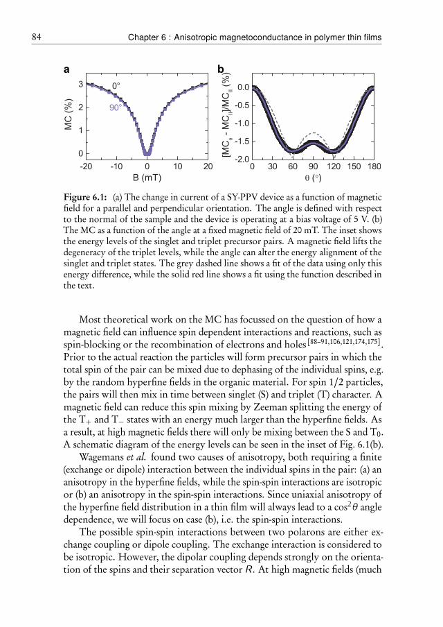
84 Chapter 6 : Anisotropic magnetoconductance in polymer thin films
a b
Figure 6.1: (a) The change in current of a SY-PPV device as a function of magneticfield for a parallel and perpendicular orientation. The angle is defined with respectto the normal of the sample and the device is operating at a bias voltage of 5 V. (b)The MC as a function of the angle at a fixed magnetic field of 20 mT. The inset showsthe energy levels of the singlet and triplet precursor pairs. A magnetic field lifts thedegeneracy of the triplet levels, while the angle can alter the energy alignment of thesinglet and triplet states. The grey dashed line shows a fit of the data using only thisenergy difference, while the solid red line shows a fit using the function described inthe text.
Most theoretical work on the MC has focussed on the question of how amagnetic field can influence spin dependent interactions and reactions, such asspin-blocking or the recombination of electrons and holes[88–91,106,121,174,175].Prior to the actual reaction the particles will form precursor pairs in which thetotal spin of the pair can be mixed due to dephasing of the individual spins, e.g.by the random hyperfine fields in the organic material. For spin 1/2 particles,the pairs will then mix in time between singlet (S) and triplet (T) character. Amagnetic field can reduce this spin mixing by Zeeman splitting the energy ofthe T+ and T− states with an energy much larger than the hyperfine fields. Asa result, at high magnetic fields there will only be mixing between the S and T0.A schematic diagram of the energy levels can be seen in the inset of Fig. 6.1(b).
Wagemans et al. found two causes of anisotropy, both requiring a finite(exchange or dipole) interaction between the individual spins in the pair: (a) ananisotropy in the hyperfine fields, while the spin-spin interactions are isotropicor (b) an anisotropy in the spin-spin interactions. Since uniaxial anisotropy ofthe hyperfine field distribution in a thin film will always lead to a cos2θ angledependence, we will focus on case (b), i.e. the spin-spin interactions.
The possible spin-spin interactions between two polarons are either ex-change coupling or dipole coupling. The exchange interaction is considered tobe isotropic. However, the dipolar coupling depends strongly on the orienta-tion of the spins and their separation vector R . At high magnetic fields (much
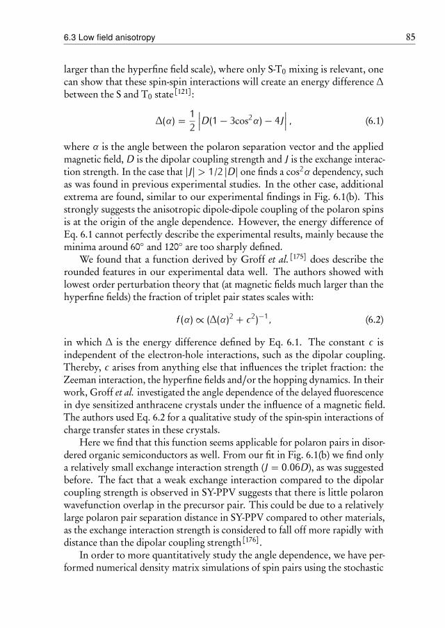
6.3 Low field anisotropy 85
larger than the hyperfine field scale), where only S-T0 mixing is relevant, onecan show that these spin-spin interactions will create an energy difference ∆between the S and T0 state[121]:
∆(α) = 12 ∣∣∣D(1− 3cos2α)− 4J∣∣∣ , (6.1)
where α is the angle between the polaron separation vector and the appliedmagnetic field, D is the dipolar coupling strength and J is the exchange interac-tion strength. In the case that |J| > 1/2 |D| one finds a cos2α dependency, suchas was found in previous experimental studies. In the other case, additionalextrema are found, similar to our experimental findings in Fig. 6.1(b). Thisstrongly suggests the anisotropic dipole-dipole coupling of the polaron spinsis at the origin of the angle dependence. However, the energy difference ofEq. 6.1 cannot perfectly describe the experimental results, mainly because theminima around 60◦ and 120◦ are too sharply defined.
We found that a function derived by Groff et al. [175] does describe therounded features in our experimental data well. The authors showed withlowest order perturbation theory that (at magnetic fields much larger than thehyperfine fields) the fraction of triplet pair states scales with:
f (α) ∝ (∆(α)2 + c2)−1, (6.2)
in which ∆ is the energy difference defined by Eq. 6.1. The constant c isindependent of the electron-hole interactions, such as the dipolar coupling.Thereby, c arises from anything else that influences the triplet fraction: theZeeman interaction, the hyperfine fields and/or the hopping dynamics. In theirwork, Groff et al. investigated the angle dependence of the delayed fluorescencein dye sensitized anthracene crystals under the influence of a magnetic field.The authors used Eq. 6.2 for a qualitative study of the spin-spin interactions ofcharge transfer states in these crystals.
Here we find that this function seems applicable for polaron pairs in disor-dered organic semiconductors as well. From our fit in Fig. 6.1(b) we find onlya relatively small exchange interaction strength (J = 0.06D), as was suggestedbefore. The fact that a weak exchange interaction compared to the dipolarcoupling strength is observed in SY-PPV suggests that there is little polaronwavefunction overlap in the precursor pair. This could be due to a relativelylarge polaron pair separation distance in SY-PPV compared to other materials,as the exchange interaction strength is considered to fall off more rapidly withdistance than the dipolar coupling strength[176].
In order to more quantitatively study the angle dependence, we have per-formed numerical density matrix simulations of spin pairs using the stochastic
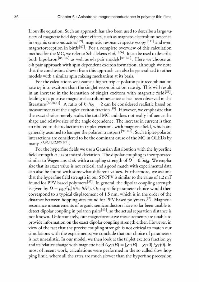
86 Chapter 6 : Anisotropic magnetoconductance in polymer thin films
Liouville equation. Such an approach has also been used to describe a large va-riety of magnetic field dependent effects, such as magneto-electroluminescencein organic semiconductors [89], magnetic resonance spectroscopy[111] and evenmagnetoreception in birds[67]. For a complete overview of this calculationmethod for the MC, we refer to Schellekens et al.[106]. It can be used to describeboth bipolaron[88,106] as well as e-h pair models [89,106]. Here we choose ane-h pair approach with spin dependent exciton formation, although we notethat the conclusions drawn from this approach can also be generalized to othermodels with a similar spin mixing mechanism at its basis.
For the calculations we assume a higher triplet polaron pair recombinationrate kT into excitons than the singlet recombination rate kS. This will resultin an increase in the formation of singlet excitons with magnetic field [89],leading to a positive magneto-electroluminescence as has been observed in theliterature[37,78,81]. A ratio of kT/kS = 2 can be considered realistic based onmeasurements of the singlet exciton fraction[89]. However, we emphasize thatthe exact choice merely scales the total MC and does not really influence theshape and relative size of the angle dependence. The increase in current is thenattributed to the reduction in triplet excitons with magnetic field, which aregenerally assumed to hamper the polaron transport[91,100]. Such triplet-polaroninteractions are considered to be the dominant cause of the MC in OLEDs bymany[73,80,91,92,100,177].
For the hyperfine fields we use a Gaussian distribution with the hyperfinefield strength σhf as standard deviation. The dipolar coupling is incorporatedsimilar to Wagemans et al. with a coupling strength of D = 0.5σhf. We empha-size that its exact value is not critical, and a good match with experimental datacan also be found with somewhat different values. Furthermore, we assumethat the hyperfine field strength in our SY-PPV is similar to the value of 1.2 mTfound for PPV based polymers[37]. In general, the dipolar coupling strengthis given by D = µ0g2µ2
B/(4πħhR3). Our specific parameter choice would thencorrespond to a typical displacement of 1.5 nm, which is in the order of thedistance between hopping sites found for PPV based polymers[17]. Magneticresonance measurements of organic semiconductors have so far been unable todetect dipolar coupling in polaron pairs [63], so the actual separation distance isnot known. Unfortunately, our magnetoresistive measurements are unable toprovide information on the exact dipolar coupling strength either. However, inview of the fact that the precise coupling strength is not critical to match oursimulations with the experiments, we conclude that our choice of parametersis not unrealistic. In our model, we then look at the triplet exciton fraction χTand its relative change with magnetic field ∆χT(B) = [χT(B)−χT(0)]/χT(0). Inmost of recent work, calculations were performed in the so called slow hop-ping limit, where all the rates are much slower than the hyperfine precession
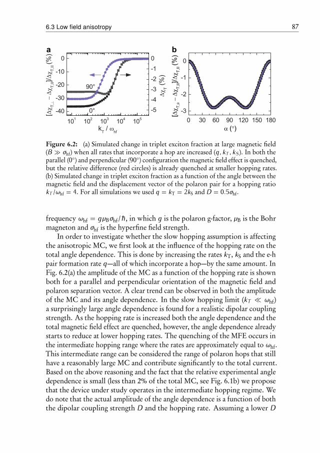
6.3 Low field anisotropy 87
a b
Figure 6.2: (a) Simulated change in triplet exciton fraction at large magnetic field(B � σhf) when all rates that incorporate a hop are increased (q, kT , kS). In both theparallel (0◦) and perpendicular (90◦) configuration the magnetic field effect is quenched,but the relative difference (red circles) is already quenched at smaller hopping rates.(b) Simulated change in triplet exciton fraction as a function of the angle between themagnetic field and the displacement vector of the polaron pair for a hopping ratiokT /ωhf = 4. For all simulations we used q = kT = 2kS and D = 0.5σhf.
frequency ωhf = gµBσhf/ħh, in which g is the polaron g-factor, µB is the Bohrmagneton and σhf is the hyperfine field strength.
In order to investigate whether the slow hopping assumption is affectingthe anisotropic MC, we first look at the influence of the hopping rate on thetotal angle dependence. This is done by increasing the rates kT, kS and the e-hpair formation rate q—all of which incorporate a hop—by the same amount. InFig. 6.2(a) the amplitude of the MC as a function of the hopping rate is shownboth for a parallel and perpendicular orientation of the magnetic field andpolaron separation vector. A clear trend can be observed in both the amplitudeof the MC and its angle dependence. In the slow hopping limit (kT � ωhf)a surprisingly large angle dependence is found for a realistic dipolar couplingstrength. As the hopping rate is increased both the angle dependence and thetotal magnetic field effect are quenched, however, the angle dependence alreadystarts to reduce at lower hopping rates. The quenching of the MFE occurs inthe intermediate hopping range where the rates are approximately equal to ωhf.This intermediate range can be considered the range of polaron hops that stillhave a reasonably large MC and contribute significantly to the total current.Based on the above reasoning and the fact that the relative experimental angledependence is small (less than 2% of the total MC, see Fig. 6.1b) we proposethat the device under study operates in the intermediate hopping regime. Wedo note that the actual amplitude of the angle dependence is a function of boththe dipolar coupling strength D and the hopping rate. Assuming a lower D
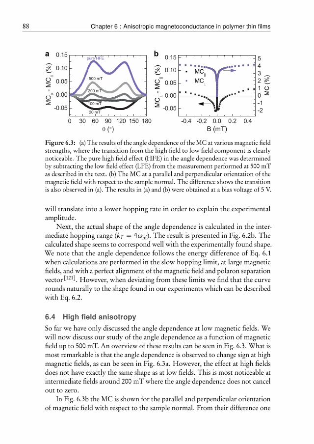
88 Chapter 6 : Anisotropic magnetoconductance in polymer thin films
a b
Figure 6.3: (a) The results of the angle dependence of the MC at various magnetic fieldstrengths, where the transition from the high field to low field component is clearlynoticeable. The pure high field effect (HFE) in the angle dependence was determinedby subtracting the low field effect (LFE) from the measurement performed at 500 mTas described in the text. (b) The MC at a parallel and perpendicular orientation of themagnetic field with respect to the sample normal. The difference shows the transitionis also observed in (a). The results in (a) and (b) were obtained at a bias voltage of 5 V.
will translate into a lower hopping rate in order to explain the experimentalamplitude.
Next, the actual shape of the angle dependence is calculated in the inter-mediate hopping range (kT = 4ωhf). The result is presented in Fig. 6.2b. Thecalculated shape seems to correspond well with the experimentally found shape.We note that the angle dependence follows the energy difference of Eq. 6.1when calculations are performed in the slow hopping limit, at large magneticfields, and with a perfect alignment of the magnetic field and polaron separationvector[121]. However, when deviating from these limits we find that the curverounds naturally to the shape found in our experiments which can be describedwith Eq. 6.2.
6.4 High field anisotropy
So far we have only discussed the angle dependence at low magnetic fields. Wewill now discuss our study of the angle dependence as a function of magneticfield up to 500 mT. An overview of these results can be seen in Fig. 6.3. What ismost remarkable is that the angle dependence is observed to change sign at highmagnetic fields, as can be seen in Fig. 6.3a. However, the effect at high fieldsdoes not have exactly the same shape as at low fields. This is most noticeable atintermediate fields around 200 mT where the angle dependence does not cancelout to zero.
In Fig. 6.3b the MC is shown for the parallel and perpendicular orientationof magnetic field with respect to the sample normal. From their difference one
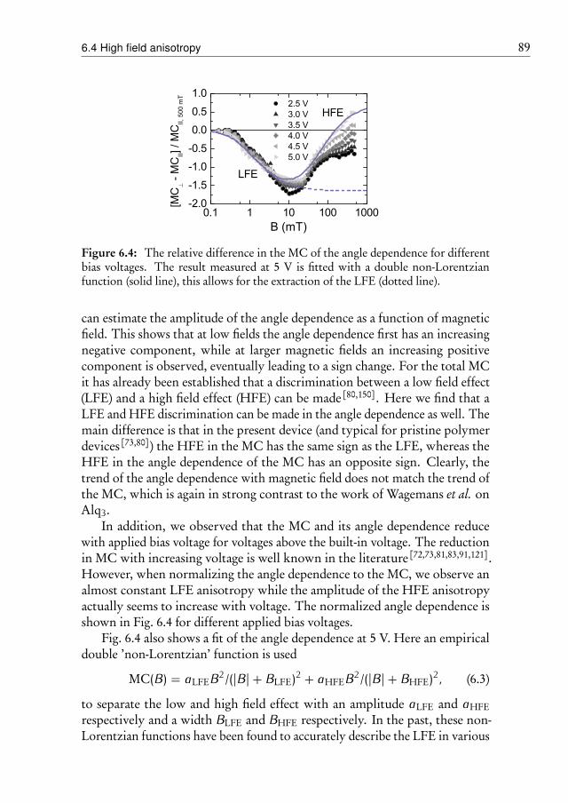
6.4 High field anisotropy 89
0.1 1 10 100 1000-2.0
-1.5
-1.0
-0.5
0.0
0.5
1.0
HFE
[MC
- M
CII]
/ MC
II, 5
00 m
T
B (mT)
2.5 V 3.0 V 3.5 V 4.0 V 4.5 V 5.0 V
LFE
Figure 6.4: The relative difference in the MC of the angle dependence for differentbias voltages. The result measured at 5 V is fitted with a double non-Lorentzianfunction (solid line), this allows for the extraction of the LFE (dotted line).
can estimate the amplitude of the angle dependence as a function of magneticfield. This shows that at low fields the angle dependence first has an increasingnegative component, while at larger magnetic fields an increasing positivecomponent is observed, eventually leading to a sign change. For the total MCit has already been established that a discrimination between a low field effect(LFE) and a high field effect (HFE) can be made [80,150]. Here we find that aLFE and HFE discrimination can be made in the angle dependence as well. Themain difference is that in the present device (and typical for pristine polymerdevices[73,80]) the HFE in the MC has the same sign as the LFE, whereas theHFE in the angle dependence of the MC has an opposite sign. Clearly, thetrend of the angle dependence with magnetic field does not match the trend ofthe MC, which is again in strong contrast to the work of Wagemans et al. onAlq3.
In addition, we observed that the MC and its angle dependence reducewith applied bias voltage for voltages above the built-in voltage. The reductionin MC with increasing voltage is well known in the literature[72,73,81,83,91,121].However, when normalizing the angle dependence to the MC, we observe analmost constant LFE anisotropy while the amplitude of the HFE anisotropyactually seems to increase with voltage. The normalized angle dependence isshown in Fig. 6.4 for different applied bias voltages.
Fig. 6.4 also shows a fit of the angle dependence at 5 V. Here an empiricaldouble ’non-Lorentzian’ function is used
MC(B) = aLFEB2/(|B|+ BLFE)2 + aHFEB2/(|B|+ BHFE)2, (6.3)
to separate the low and high field effect with an amplitude aLFE and aHFErespectively and a width BLFE and BHFE respectively. In the past, these non-Lorentzian functions have been found to accurately describe the LFE in various
90 Chapter 6 : Anisotropic magnetoconductance in polymer thin films
materials[46] and numerical spin density matrix calculations can also accountfor such functions [88,106]. Using two non-Lorentzians to discriminate betweenthe LFE and HFE is an approach that has already been used in the litera-ture [80,150]. With this approach it is possible to extrapolate the size of theLFE at large magnetic fields. Thereby, one can subtract the low field angledependence from the high field results to find the pure HFE component. InFig. 6.3a we have shown the pure HFE MC as a function of the angle.
At high fields the Zeeman interaction is much larger than the hyperfineinteraction. Therefore, changes in spin mixing have to be attributed to anothermechanism. Several suggestions have been proposed for the HFE in the lit-erature, an overview of these is given by Schellekens et al.[106]. One distinctHFE is called the ∆g-mechanism, where a (slight) difference in g-factor of thepolarons is considered to lead to a different spin precession at high fields andthus more spin mixing. Additionally, the reaction of triplet excitons either withpolarons or other triplet excitons is spin dependent and considered to cause ahigh field effect. The linewidth of the high field component is then attributedto the zero field splitting (ZFS) of the triplet exciton, which is generally abouttwo orders of magnitude larger than the hyperfine interaction [178]. In theremainder of this section, we will investigate these possible mechanisms for thehigh field effect and its anisotropy. Similar to the LFE, we performed numeri-cal density matrix calculations of spin pairs. However, we will find that thesemechanisms cannot unambiguously explain the observed HFE anisotropy.
The most unlikely candidate for the HFE and its angle dependence in thepresent system is the ∆g-mechanism. First of all, an unrealistically large g-factor difference is required to obtain a HFE in the correct field range. Secondly,the HFE in the MC will always have a sign opposite to the LFE. Both of thesearguments have already been made in the literature[106]. Additionally, therewill be no change in the shape of the angle dependence as we observe in ourexperiments, because the anisotropy in the HFE has the same origin as theLFE, i.e. the dipolar coupling. All of these arguments are also confirmed byour density matrix calculations, shown in Fig. 6.5a,b. The MC as a function ofmagnetic field shown in Fig. 6.5a clearly shows the opposite sign of the HFE.The angle dependence of this HFE will reduce to zero at large magnetic fields,which can also be seen in Fig. 6.5b. We note that the g-factor itself could alsobe slightly anisotropic. However, Wagemans et al. already excluded this as apossible origin for the angle dependence, because it is generally negligible indisordered organic semiconductors[121].
This leaves us with a triplet based mechanism. Such a mechanism can have acompletely different kind of anisotropy compared to a polaron pair spin mixingmechanism, since it can have anisotropy in the zero field splitting of the tripletexciton. This might explain why the HFE has a different angle dependence than
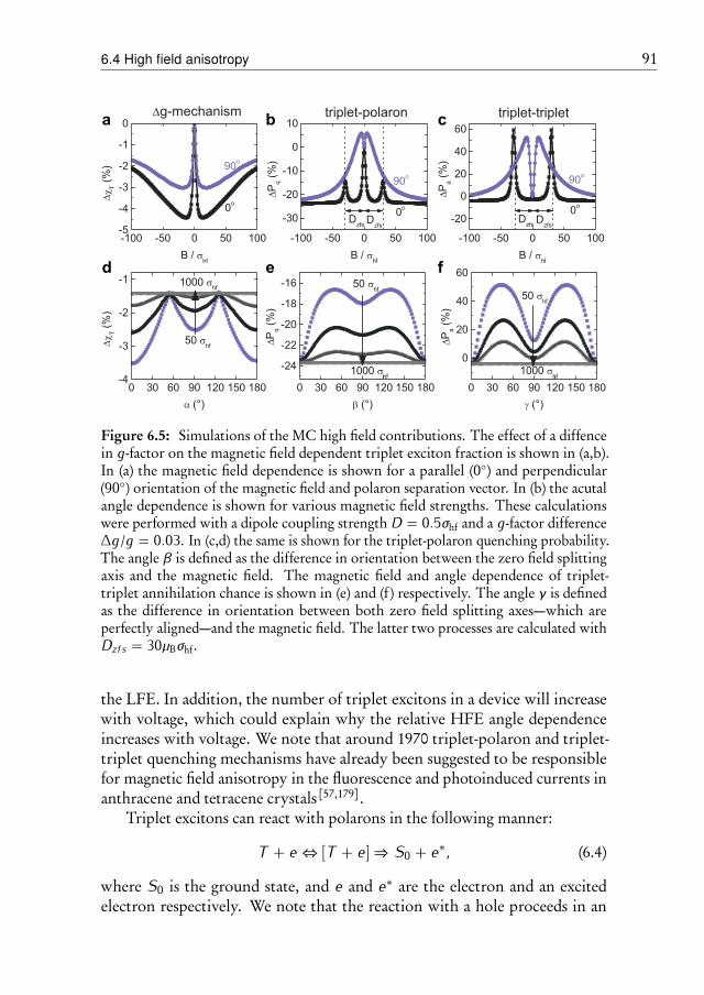
6.4 High field anisotropy 91
a b c
d e f
Figure 6.5: Simulations of the MC high field contributions. The effect of a diffencein g-factor on the magnetic field dependent triplet exciton fraction is shown in (a,b).In (a) the magnetic field dependence is shown for a parallel (0◦) and perpendicular(90◦) orientation of the magnetic field and polaron separation vector. In (b) the acutalangle dependence is shown for various magnetic field strengths. These calculationswere performed with a dipole coupling strength D = 0.5σhf and a g-factor difference∆g/g = 0.03. In (c,d) the same is shown for the triplet-polaron quenching probability.The angle β is defined as the difference in orientation between the zero field splittingaxis and the magnetic field. The magnetic field and angle dependence of triplet-triplet annihilation chance is shown in (e) and (f) respectively. The angle γ is definedas the difference in orientation between both zero field splitting axes—which areperfectly aligned—and the magnetic field. The latter two processes are calculated withDzfs = 30µBσhf.
the LFE. In addition, the number of triplet excitons in a device will increasewith voltage, which could explain why the relative HFE angle dependenceincreases with voltage. We note that around 1970 triplet-polaron and triplet-triplet quenching mechanisms have already been suggested to be responsiblefor magnetic field anisotropy in the fluorescence and photoinduced currents inanthracene and tetracene crystals[57,179].
Triplet excitons can react with polarons in the following manner:
T + e⇔ [T + e]⇒ S0 + e∗, (6.4)
where S0 is the ground state, and e and e∗ are the electron and an excitedelectron respectively. We note that the reaction with a hole proceeds in an
92 Chapter 6 : Anisotropic magnetoconductance in polymer thin films
identical way. The reaction in Eq. 6.4 has been suggested in the literature tosignificantly influence the current[73,91], either by releasing trapped polaronsor by trapping of free polarons. The reaction to the ground state (last step inEq. 6.4) is only possible if the total spin state of the triplet-polaron pair is 1/2,which means it needs to have a doublet character. Therefore, we have, similarto Schellekens et al., calculated the probability Pq that the triplet-polaron pairis quenched. This density matrix implementation also incorporates a triplet-polaron pair formation rate k1 and dissociation rate k−1 into free triplets.Additionally, it has a quenching rate k2 towards the ground state when the pairhas a doublet character.
For the triplet-triplet reaction we take a similar approach. Two tripletexcitons can annihilate and create a ground state and a singlet exciton:
T + T ⇔ [T + T ]⇒ S0 + S1. (6.5)
Spin conservation rules require the triplet-triplet pair to have zero total spinin order to annihilate, i.e. it needs a singlet character. For that reason, wecalculated the effect of a magnetic field on the annihilation chance Pa via asinglet state. This density matrix implementation also incorporates a triplet-triplet pair formation rate k3, dissociation rate k−3 and annihilation rate k4towards the ground state when the pair has a singlet character[106]. A zerofield splitting parameter Dzfs = 30σhf is taken for both the triplet-polaron andtriplet-triplet reaction. The results of our calculations for triplet-polaron andtriplet-triplet interactions are shown in Fig. 6.5c-f.
The downside of taking a single zero field splitting axis, i.e. a single molec-ular orientation, is that our calculations show features that are clearly notobserved in the experiments. When the magnetic field is aligned parallel tothe ZFS axis, there will be strong level crossing resonances at the magneticfield strength equal to Dzfs. At these level crossings, states that were initiallynondegenerate at zero magnetic field due to the zero field splitting becomedegenerate, resulting in additional spin mixing. In the literature it is known thatthese features average out when averaging over all molecular orientations[106].Additionally, so called ‘anti-crossings’ could affect or cause an absence of thesepeaks[180].
The angle dependence at large magnetic fields does look different than theangle dependence caused the ∆g-mechanism. At a first glance, this suggests thatanisotropic triplet quenching mechanisms could be at the origin of the high fieldcomponent. However, what is clear from our calculations is that the amplitudeof the angle dependence of such triplet quenching mechanisms will reduce withincreasing magnetic fields. This is in contrast to the experimental results shownin Fig. 6.3 and Fig. 6.4, where the high field anisotropy is observed to increasewith magnetic field. Therefore, we conclude that triplet quenching mechanismscan also not unambiguously explain the high field anisotropy.
6.5 Conclusion 93
6.5 Conclusion
In conclusion, using experiments and spin density matrix calculations weinvestigated the source of anisotropy in the magnetic field sensitive current ofthe organic semiconducting polymer ‘Super Yellow’ PPV. Both a low and highfield component were identified. The shape of the angle dependence of the lowfield component of the MC can be explained by anisotropic dipolar coupling.The amplitude of this low field component can most readily be explained if thedevice is assumed to operate in the intermediate hopping regime. In addition,the experimental results show an anisotropic high field contribution withopposite sign, slightly different shape as a function of the angle and alternativevoltage dependence compared to the low field contribution. A difference ing-factor is an unlikely candidate for this high field component. Reactions oftriplet excitons with other spin carrying particles are more likely candidates,though they can not fully explain the observed magnetic field dependence ofthe anisotropy either. These results suggests a more solid theoretical model isrequired for the high field effects.

7∆B-mechanism for fringe-fieldorganic magnetoresistance
Fringe fields emanating from magnetic domain structures can give rise to magne-toresistance in organic semiconductors. In this article, we explain these magneticfield effects in terms of a ∆B-mechanism. This mechanism describes how variationsin magnetic field strength between two polaron hopping sites can induce a differ-ence in precessional motion of the polaron spins, leading to mixing of their spinstates. In order to experimentally explore the fringe field effects, polymer thin filmdevices on top of a rough in-plane magnetized cobalt layer are investigated. Thecobalt layer can be described by a distribution of out-of-plane magnetic anisotropies.With a magnetic field perpendicular to the cobalt layer, fringe fields are createdbecause some domains are magnetized out of plane while the magnetization ofother domains remains approximately in plane. By varying the distance betweenthe polymer layer and the cobalt layer, we find that the magnetoresistance arisingfrom these fringe fields reduces with the gradient in the fringe fields, in agreementwith the ∆B-mechanism.
Manuscript submitted to Physical Review B
95
96 Chapter 7 : ∆B-mechanism for fringe-field organic magnetoresistance
7.1 Introduction
Many organic semiconducting devices exhibit intrinsic magnetic field effectsin their conductive or luminescent properties at low magnetic fields[46]. Thismakes organic semiconductors interesting for magnetic field sensing applica-tions[49]. Local hyperfine fields are involved in the origin of these magnetic fieldeffects[37]. These hyperfine fields can cause mixing, or intersystem crossing, ofspin states. The suppression of this spin mixing by an applied magnetic field isbelieved to be responsible for the magnetic field effects[60,89]. Unfortunately,relying on hyperfine fields offers only very little control over the amount ofspin mixing. They are determined by the organic material itself and vary onlylittle between different materials. However, there are also other sources ofspin mixing. In particular, the (inhomogeneous) fringe fields emanating frommagnetic domains or nanoparticles could play a role similar to that of hyperfinefields[181]. Such fringe fields depend on the properties of the magnetic material,which can be controlled, for example, by patterning.
Recently, this idea was applied to organic semiconductors by Wang etal.[50] In their work the magnetoconductance in an organic device on top of aferromagnetic layer was shown to depend on the magnetized state of the layer.In the presence of fringe fields emanating from the magnetic domains in thislayer, the magnetoconductance was found to decrease significantly. Controlexperiments showed that the observed effect was not related to spin injection.An explanation based on mixing of spin states of a spin pair on adjacent sitesprior to their reaction (‘two-site model’) by differently oriented magnetic fieldsat these sites was dismissed by the authors, because of the large correlationlength of the fringe fields, resulting in almost completely aligned fields atadjacent sites. On the other hand, Harmon et al. recently suggested the fringefield gradients might cause additional spin mixing[182]. These gradients are inthe order of a few millitesla per nanometer, which is comparable to the size ofthe hyperfine fields.
In this manuscript, we will show that a straightforward two-site modelcan explain the enhanced spin mixing due to the fringe field gradients, evenat large applied magnetic fields. A small difference in magnetic field ∆B atthe two sites can lead to a difference in precession frequency of the two spinsand hence to mixing between their spin states. Because this mechanism issimilar to the so-called ∆g-mechanism, we coin it the ∆B-mechanism. Weinvestigate devices with a magnetic layer causing fringe fields in the activeorganic layer. By increasing the distance between the magnetic and active layerthe magnetoresistance caused by the fringe fields decreases. The reduction ofthis fringe-field magnetoresistance is found to correlate well with the calculateddistance dependence of the fringe field gradients emanating from the magneticlayer.
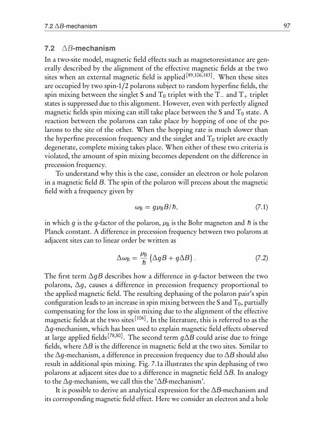
7.2 ∆B-mechanism 97
7.2 ∆B-mechanism
In a two-site model, magnetic field effects such as magnetoresistance are gen-erally described by the alignment of the effective magnetic fields at the twosites when an external magnetic field is applied[89,106,183]. When these sitesare occupied by two spin-1/2 polarons subject to random hyperfine fields, thespin mixing between the singlet S and T0 triplet with the T− and T+ tripletstates is suppressed due to this alignment. However, even with perfectly alignedmagnetic fields spin mixing can still take place between the S and T0 state. Areaction between the polarons can take place by hopping of one of the po-larons to the site of the other. When the hopping rate is much slower thanthe hyperfine precession frequency and the singlet and T0 triplet are exactlydegenerate, complete mixing takes place. When either of these two criteria isviolated, the amount of spin mixing becomes dependent on the difference inprecession frequency.
To understand why this is the case, consider an electron or hole polaronin a magnetic field B. The spin of the polaron will precess about the magneticfield with a frequency given by
ωB = gµBB/ħh, (7.1)
in which g is the g-factor of the polaron, µB is the Bohr magneton and ħh is thePlanck constant. A difference in precession frequency between two polarons atadjacent sites can to linear order be written as
∆ωB = µB
ħh(∆gB + g∆B) . (7.2)
The first term ∆gB describes how a difference in g-factor between the twopolarons, ∆g, causes a difference in precession frequency proportional tothe applied magnetic field. The resulting dephasing of the polaron pair’s spinconfiguration leads to an increase in spin mixing between the S and T0, partiallycompensating for the loss in spin mixing due to the alignment of the effectivemagnetic fields at the two sites [106]. In the literature, this is referred to as the∆g-mechanism, which has been used to explain magnetic field effects observedat large applied fields [78,80]. The second term g∆B could arise due to fringefields, where ∆B is the difference in magnetic field at the two sites. Similar tothe ∆g-mechanism, a difference in precession frequency due to ∆B should alsoresult in additional spin mixing. Fig. 7.1a illustrates the spin dephasing of twopolarons at adjacent sites due to a difference in magnetic field ∆B. In analogyto the ∆g-mechanism, we call this the ‘∆B-mechanism’.
It is possible to derive an analytical expression for the ∆B-mechanism andits corresponding magnetic field effect. Here we consider an electron and a hole
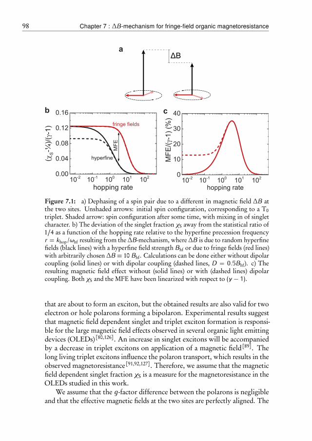
98 Chapter 7 : ∆B-mechanism for fringe-field organic magnetoresistance
ΔBa
b c
Figure 7.1: a) Dephasing of a spin pair due to a different in magnetic field ∆B atthe two sites. Unshaded arrows: initial spin configuration, corresponding to a T0triplet. Shaded arrow: spin configuration after some time, with mixing in of singletcharacter. b) The deviation of the singlet fraction χS away from the statistical ratio of1/4 as a function of the hopping rate relative to the hyperfine precession frequencyr = khop/ωhf resulting from the ∆B-mechanism, where ∆B is due to random hyperfinefields (black lines) with a hyperfine field strength Bhf or due to fringe fields (red lines)with arbitrarily chosen ∆B = 10 Bhf. Calculations can be done either without dipolarcoupling (solid lines) or with dipolar coupling (dashed lines, D = 0.5Bhf). c) Theresulting magnetic field effect without (solid lines) or with (dashed lines) dipolarcoupling. Both χS and the MFE have been linearized with respect to (γ − 1).that are about to form an exciton, but the obtained results are also valid for twoelectron or hole polarons forming a bipolaron. Experimental results suggestthat magnetic field dependent singlet and triplet exciton formation is responsi-ble for the large magnetic field effects observed in several organic light emittingdevices (OLEDs) [80,126]. An increase in singlet excitons will be accompaniedby a decrease in triplet excitons on application of a magnetic field [89]. Thelong living triplet excitons influence the polaron transport, which results in theobserved magnetoresistance [91,92,127]. Therefore, we assume that the magneticfield dependent singlet fraction χS is a measure for the magnetoresistance in theOLEDs studied in this work.
We assume that the g-factor difference between the polarons is negligibleand that the effective magnetic fields at the two sites are perfectly aligned. The
7.2 ∆B-mechanism 99
latter would correspond to the case where a large external magnetic field isapplied (in the z-direction). The spin Hamiltonian of this system is given by
H = gµBBeSz,e/ħh+ gµBBhSz,h/ħh, (7.3)
in which Sz,e(h) is the spin operator in the z-direction for the electron (hole).The steady-state fraction of singlet excitons χS that is formed from polaronpairs can be derived using a stochastic Liouville equation[89,106]. We investigatepolaron pairs that are formed with a rate ku and from which singlet and tripletexcitons are created with rates kS and kT, respectively. Because large alignedmagnetic fields are assumed, mixing with the T− and T+ is suppressed dueto the large Zeeman interaction. Therefore, these states can be neglected inthe deriviation. The steady-state density operator is found by demandingtime-independence of the stochastic Liouville equation:
0 = ∂ρ∂t = − i
ħh [H, ρ]− 12 {Λ, ρ}+ Γ, (7.4)
in which Λ = Σλkλ|λ〉〈λ|, with λ = S, T0 and Γ = kuI/4, where I is the identityoperator. As formation rates, we take kT = khop/γ and kS = khop. Here γ istaken as the ratio between the singlet and triplet exciton formation rates, whichhave to be different to obtain magnetic field dependent exciton fractions [89].From the obtained density matrix one can straightforwardly derive the singletexciton fraction χS, which is given by:
χS = γ1 + γ14(2− γ − 1(gµB∆Bγ/khopħh)2 + γ
). (7.5)
Figure 7.1b shows how χS evolves with the relative hopping rate for ∆B =10Bhf (solid black curve). Because γ is generally considered to be close tounity[89], we have linearized χS with respect to (γ − 1) in order to show themost general result. The relative hopping rate is defined as r = khop/ωhf,with the hyperfine frequency ωhf = gµBBhf/ħh at a hyperfine field Bhf. Thestatistical singlet fraction is 1/4, but spin mixing changes it to γ/2(1 + γ) atslow hopping (r � 1). When the hopping rate increases, the exciton formationrate becomes faster than the precession frequency, thereby quenching the spinmixing. The transition occurs around r = ∆B√γ/Bhf.
In the absence of fringe fields, the hyperfine fields are still capable of causingmixing between the S and T0 states. With a large external magnetic field B~z,∆B is given by the difference in the z-component of the hyperfine fields. ∆Bcan then be described with a Gaussian distribution with standard deviation2Bhf. Averaging Eq. 7.5 over the hyperfine fields is done analytically (not
100 Chapter 7 : ∆B-mechanism for fringe-field organic magnetoresistance
shown here). As can be seen in Fig. 7.1b, the transition from the slow-hoppingto the fast-hopping result is slighty less abrupt than with a fixed ∆B. Note thatin reality the gradient in the fringe fields experienced by all the polarons in adevice may also have a certain distribution.
In the transition from slow to fast hopping, the spin mixing is graduallyquenched. When polarons form excitons with intermediate hopping rates,we find that the amount of spin mixing and thus the singlet exciton fractiondepends on the strength of ∆B. By controlling the fringe fields, e.g. withdomains in a magnetic layer, the singlet and triplet exciton fractions can beinfluenced and hence the magnetoresistance.
The above describes the main aspects of the ∆B-mechanism, but otheringredients can be added. For example, incomplete spin mixing arises at slowhopping rates due spin-spin interactions in the form of dipolar coupling orexchange interaction, because these lead to an energy difference between S andT0. Dipolar coupling generally dominates the exchange interaction at largerdistances [176]. Therefore, we will here consider how dipolar coupling influencesthe ∆B-mechanism. For the case that the two polarons are separated from eachother in the z-direction (assuming polaron transport takes place along themagnetic field), the following term has to be added to the Hamiltonian:
Hdip = −2gµBDSz,eSz,h/ħh, (7.6)
in which the dipolar coupling strength is given by D = µ0gµB/(4πR3). For atypical separation distance R of 1.5 nm [17] and a hyperfine field strength of1 mT[37] the dipolar coupling strength would be equivalent to D = 0.5Bhf,but the exact coupling strength is not critical for the present work. Similarto the derivation above, it is possible to find a density matrix from the steadystate solution of Eq. 7.4. The result for χS with dipolar coupling is also shownin Fig. 7.1b (dashed lines). Essentially, the spin-spin interactions suppress thespin mixing and shift the singlet fraction towards the statistical ratio of 1/4.The amount of suppression depends on the relative strength of D/∆B, whichexplains why the effect is best observed for the calculation with the hyperfinefields. With the addition of a larger ∆B due to the fringe fields, spin mixing canthus also be increased at slow hopping rates.
The singlet and triplet fractions and other quantities that depend on them,such as the current, are magnetic field dependent. The singlet fractions derivedabove are the saturated values at large magnetic fields. As we have shown,these values depend on the size of ∆B, which can be increased by ‘turning on’fringe fields. One can define a relative magnetic field effect caused by the fringefields as (χS,hf − χS,fringe)/χS,fringe. This magnetic field effect (MFE) is shownin Fig. 7.1c as a function of the relative hopping rate. The size of this MFE
7.3 Fringe-field magnetoresistance 101
depends on the hopping rate, spin-spin interactions and the dynamics of thespin-dependent processes (the latter is included in γ for the case of excitonformation).
7.3 Fringe-field magnetoresistance
In order to investigate the influence of fringe fields on the magnetoresistance,we fabricated devices with a layer stack similar to OLEDs, only with a mag-netic cobalt layer inserted close to the organic layer. In contrast to previouswork[50,184,185], we use a single (rough) cobalt layer with an in-plane magne-tization due to shape anisotropy. The cobalt layer can be placed on a seedlayer underneath the functional device or on top of the device, however, theexperiments in this work will focus on devices with a cobalt layer on top.By applying a magnetic field in-plane or out-of-plane the fringe fields can beturned off and on respectively, making this a convenient system to study themagnetoresistance arising from fringe fields. A Superconducting Quantum In-terference Device (SQUID) was used to characterize the magnetic properties ofthe cobalt layers and Atomic Force Microscopy (AFM) was used to investigatetheir roughness.
The results of the magnetization and roughness are shown in Fig. 7.2a,b fora cobalt layer on top of an aluminum seed layer. We note that we found similarresults for cobalt layers on top of an organic layer. As expected, when themagnetic field is applied in plane, we find an abrupt switch with a coercive fieldof 1.2 mT. When the magnetic field is applied out of plane, the magnetizationslowly reaches saturation at more than 1.5 T. For an ideal in-plane magnetizedlayer the magnetization should follow a linear function according to Stoner-Wohlfarth theory [186]. However, we find two regimes; at fields roughly below200 mT the magnetization changes more rapidly than at higher fields. Theexistence of these two regimes can be explained from the roughness of the layer,shown in Fig. 7.2b, leading to different local out-of-plane shape anisotropies.In some regions the layer is thicker than in other regions and in these regionsthe magnetization may be pulled out of plane more easily. The fact that thereare two distinct regimes is indicative of two separate distributions of shapeanisotropies. This means that at a magnetic field around the transition betweenthese two regimes, some parts of the cobalt layer are completely magnetizedout of plane, while the other parts hardly are.
Fringe fields occur when a magnetic layer has domains with different mag-netizations. Based on the magnetic characterization, a rough cobalt layer canthus be used to create fringe fields by applying moderate out-of-plane mag-netic fields. The devices consist of glass substrates with pre-patterned indiumtin oxide (ITO) and 40 nm of spincoated poly(3,4-ethylenedioxythiophene):
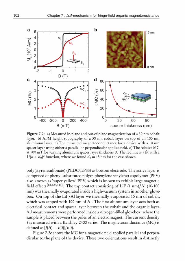
102 Chapter 7 : ∆B-mechanism for fringe-field organic magnetoresistance
B┴
B||
MC┴
MC||
M┴
M||
CoAl
PPV
15 nm
0 nm
a b
c d
Figure 7.2: a) Measured in-plane and out-of-plane magnetization of a 30 nm cobaltlayer. b) AFM height topography of a 30 nm cobalt layer on top of an 100 nmaluminum layer. c) The measured magnetoconductance for a device with a 10 nmspacer layer using either a parallel or perpendicular applied field. d) The relative MCat 500 mT for varying aluminum spacer layer thickness d. The red line is a fit with a1/(d+ d0)2 function, where we found d0 = 15 nm for the case shown.
poly(styrenesulfonate) (PEDOT:PSS) as bottom electrode. The active layer iscomprised of phenyl-substituted poly(p-phenylene vinylene) copolymer (PPV)also known as ’super yellow’ PPV, which is known to exhibit large magneticfield effects[81,127,149]. The top contact consisting of LiF (1 nm)/Al (10-100nm) was thermally evaporated inside a high-vacuum system in another glove-box. On top of the LiF/Al layer we thermally evaporated 15 nm of cobalt,which was capped with 100 nm of Al. The first aluminum layer acts both aselectrical contact and spacer layer between the cobalt and the organic layer.All measurements were performed inside a nitrogen-filled glovebox, where thesample is placed between the poles of an electromagnet. The current densityJ is measured with a Keithley 2400 series. The magnetoconductance (MC) isdefined as [J(B)− J(0)]/J(0).
Figure 7.2c shows the MC for a magnetic field applied parallel and perpen-dicular to the plane of the device. These two orientations result in distinctly
7.4 Fringe-field magnetoresistance calculations 103
different responses. For a parallel orientation we find a monotonously in-creasing MC, which is generally found in the literature for standard OLEDdevices[46,81,91,127]. For a perpendicular magnetic field the MC first followsthis trend, but then deviates from it and eventually even decreases again. Thisdeviation occurs at the transition between the two regimes in the magnetizationmeasurement in Fig. 7.2a, where domains with different magnetization arepresent. Wang et al. also found a reduction of the MC when magnetic domainsin the magnetic layer are created. This reduction is indicative of enhancedspin mixing due to the presence of fringe fields, as can be explained with the∆B-mechanism. At larger field we expect the perpendicular MC to returnto the value of the parallel MC, because then the entire cobalt layer will bemagnetized in the same direction, leading to vanishing fringe fields. However,our measurement setup is unable to reach such fields.
The same measurements were performed with varying aluminum spacerthickness. Fig. 7.2d shows the relative difference in MC at 500 mT (δMC =(MC||−MC⊥)/MC||) as a function of the spacer thickness. The δMC is normal-ized with respect to the regular (hyperfine) MC given by MC|| to account fordevice variations in the MC. As the organic layer is further separated from themagnetic layer, the fringe fields in the organic layer will reduce. Accordingly,the relative MC reduces with increasing spacer thickness, as can be observedin Figure 7.2d. We find that this reduction can be described with a (d+ d0)−2function, where d is the spacer thickness and d0 an offset distance. Note thatthe relative MC will not completely approach zero at large d, because of asmall intrinsic angle dependence[86]. In the next section, we will show that thegradients in the fringe fields are also expected to follow a similar dependence asa function of the distance away from the magnetic layer. The d−2 dependencecan readily be understood intuitively. For a magnetic dipole, the magnetic fieldreduces with 1/R3, where R is de distance from the dipole. After performing asurface integral, the magnetic field depends on distance d to the plane as 1/dand its gradient as 1/d2. The offset distance could arise, because the relevantpolaron pairs are not positioned at d = 0, but some distance away from theplane into the organic layer. Therefore, d0 might be related to the location ofthe recombination region. We will show in the next section that d0 can alsobe related to the magnetic domain structure. Finally, we note that our resultsshow that with a hybrid device the weak intrinsic angle dependence of organicmagnetoresistance can be enhanced by the insertion of magnetic materials withangle dependent fringe fields.
7.4 Fringe-field magnetoresistance calculations
In order to investigate how the fringe-field magnetoresistance depends on thedistance to the magnetic layer, we use the ∆B-mechanism and a straightforward
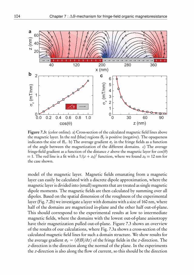
104 Chapter 7 : ∆B-mechanism for fringe-field organic magnetoresistance
x (nm)
z (
nm
)
40 120 200 280 360
20
40
60
θ
a
b c
Figure 7.3: (color online). a) Cross-section of the calculated magnetic field lines abovethe magnetic layer. In the red (blue) regions Bz is positive (negative). The opaquenessindicates the size of Bz . b) The average gradient σz in the fringe fields as a functionof the angle between the magnetization of the different domains. c) The averagefringe-field gradient as a function of the distance z above the magnetic layer for cos(θ)= 1. The red line is a fit with a 1/(z + z0)2 function, where we found z0 = 12 nm forthe case shown.
model of the magnetic layer. Magnetic fields emanating from a magneticlayer can easily be calculated with a discrete dipole approximation, where themagnetic layer is divided into (small) segments that are treated as single magneticdipole moments. The magnetic fields are then calculated by summing over alldipoles. Based on the spatial dimension of the roughness of the experimentallayer (Fig. 7.2b) we investigate a layer with domains with a size of 160 nm, wherehalf of the domains are magnetized in-plane and the other half out-of-plane.This should correspond to the experimental results at low to intermediatemagnetic fields, where the domains with the lowest out-of-plane anisotropyhave their magnetization pulled out-of-plane. Figure 7.3 shows an overviewof the results of our calculations, where Fig. 7.3a shows a cross-section of thecalculated magnetic field lines for such a domain structure. We show results forthe average gradient σz = 〈∂|B|/∂z〉 of the fringe fields in the z-direction. Thez-direction is the direction along the normal of the plane. In the experimentsthe z-direction is also along the flow of current, so this should be the direction
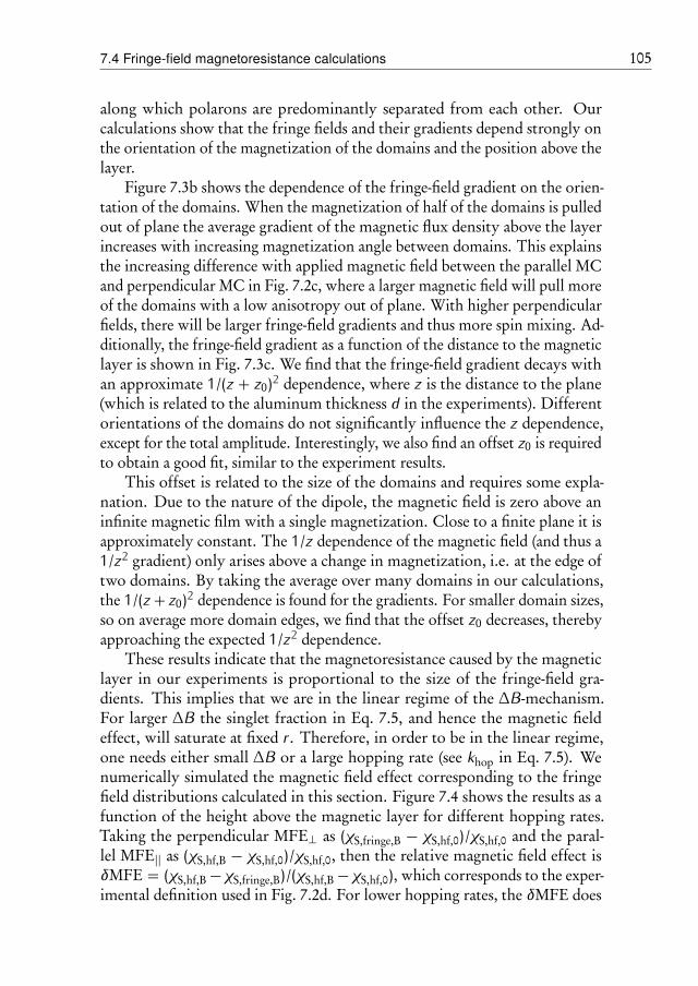
7.4 Fringe-field magnetoresistance calculations 105
along which polarons are predominantly separated from each other. Ourcalculations show that the fringe fields and their gradients depend strongly onthe orientation of the magnetization of the domains and the position above thelayer.
Figure 7.3b shows the dependence of the fringe-field gradient on the orien-tation of the domains. When the magnetization of half of the domains is pulledout of plane the average gradient of the magnetic flux density above the layerincreases with increasing magnetization angle between domains. This explainsthe increasing difference with applied magnetic field between the parallel MCand perpendicular MC in Fig. 7.2c, where a larger magnetic field will pull moreof the domains with a low anisotropy out of plane. With higher perpendicularfields, there will be larger fringe-field gradients and thus more spin mixing. Ad-ditionally, the fringe-field gradient as a function of the distance to the magneticlayer is shown in Fig. 7.3c. We find that the fringe-field gradient decays withan approximate 1/(z + z0)2 dependence, where z is the distance to the plane(which is related to the aluminum thickness d in the experiments). Differentorientations of the domains do not significantly influence the z dependence,except for the total amplitude. Interestingly, we also find an offset z0 is requiredto obtain a good fit, similar to the experiment results.
This offset is related to the size of the domains and requires some expla-nation. Due to the nature of the dipole, the magnetic field is zero above aninfinite magnetic film with a single magnetization. Close to a finite plane it isapproximately constant. The 1/z dependence of the magnetic field (and thus a1/z2 gradient) only arises above a change in magnetization, i.e. at the edge oftwo domains. By taking the average over many domains in our calculations,the 1/(z+ z0)2 dependence is found for the gradients. For smaller domain sizes,so on average more domain edges, we find that the offset z0 decreases, therebyapproaching the expected 1/z2 dependence.
These results indicate that the magnetoresistance caused by the magneticlayer in our experiments is proportional to the size of the fringe-field gra-dients. This implies that we are in the linear regime of the ∆B-mechanism.For larger ∆B the singlet fraction in Eq. 7.5, and hence the magnetic fieldeffect, will saturate at fixed r. Therefore, in order to be in the linear regime,one needs either small ∆B or a large hopping rate (see khop in Eq. 7.5). Wenumerically simulated the magnetic field effect corresponding to the fringefield distributions calculated in this section. Figure 7.4 shows the results as afunction of the height above the magnetic layer for different hopping rates.Taking the perpendicular MFE⊥ as (χS,fringe,B − χS,hf,0)/χS,hf,0 and the paral-lel MFE|| as (χS,hf,B − χS,hf,0)/χS,hf,0, then the relative magnetic field effect isδMFE = (χS,hf,B−χS,fringe,B)/(χS,hf,B−χS,hf,0), which corresponds to the exper-imental definition used in Fig. 7.2d. For lower hopping rates, the δMFE does
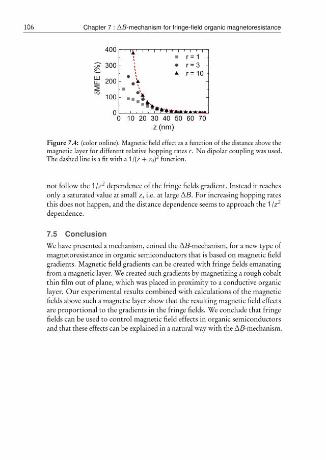
106 Chapter 7 : ∆B-mechanism for fringe-field organic magnetoresistance
0 10 20 30 40 50 60 700
100
200
300
400
r = 1 r = 3 r = 10
MFE
(%)
z (nm)
Figure 7.4: (color online). Magnetic field effect as a function of the distance above themagnetic layer for different relative hopping rates r. No dipolar coupling was used.The dashed line is a fit with a 1/(z + z0)2 function.
not follow the 1/z2 dependence of the fringe fields gradient. Instead it reachesonly a saturated value at small z, i.e. at large ∆B. For increasing hopping ratesthis does not happen, and the distance dependence seems to approach the 1/z2dependence.
7.5 Conclusion
We have presented a mechanism, coined the ∆B-mechanism, for a new type ofmagnetoresistance in organic semiconductors that is based on magnetic fieldgradients. Magnetic field gradients can be created with fringe fields emanatingfrom a magnetic layer. We created such gradients by magnetizing a rough cobaltthin film out of plane, which was placed in proximity to a conductive organiclayer. Our experimental results combined with calculations of the magneticfields above such a magnetic layer show that the resulting magnetic field effectsare proportional to the gradients in the fringe fields. We conclude that fringefields can be used to control magnetic field effects in organic semiconductorsand that these effects can be explained in a natural way with the ∆B-mechanism.
8Future research and applicationsof organic spintronics
In recent years, much advancement has been made in the application of organicmaterials for spintronics. Here we investigate several ongoing and novel avenuesfor future research. First the possibility to sense individual magnetic domain wallsis described, which could result in the application of a nanoscale, molecular sensorto read out magnetic information. Then we discuss research opportunities forspin-polarized transport and detection with organic materials in order to improveour insights into organic spin valve technology. Finally, this chapter ends withseveral proposals to engineer organic magnetoresistance based the insights gainedfrom this thesis, in order to make organic magnetoresistance more appealing forfuture applications.
107
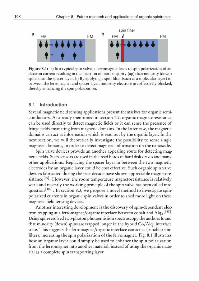
108 Chapter 8 : Future research and applications of organic spintronics
FM FM FM FM
spin filtera b
Figure 8.1: a) In a typical spin valve, a ferromagnet leads to spin polarization of anelectron current resulting in the injection of more majority (up) than minority (down)spins into the spacer layer. b) By applying a spin filter (such as a molecular layer) inbetween the ferromagnet and spacer layer, minority electrons are effectively blocked,thereby enhancing the spin polarization.
8.1 Introduction
Several magnetic field sensing applications present themselves for organic semi-conductors. As already mentioned in section 1.2, organic magnetoresistancecan be used directly to detect magnetic fields or it can sense the presence offringe fields emanating from magnetic domains. In the latter case, the magneticdomains can act as information which is read out by the organic layer. In thenext section, we will theoretically investigate the possibility to sense singlemagnetic domains, in order to detect magnetic information on the nanoscale.
Spin valve devices provide an another appealing route for detecting mag-netic fields. Such sensors are used in the read heads of hard disk drives and manyother applications. Replacing the spacer layer in between the two magneticelectrodes by an organic layer could be cost effective. Such organic spin valvedevices fabricated during the past decade have shown appreciable magnetore-sistance[40]. However, the room temperature magnetoresistance is relativelyweak and recently the working principle of the spin valve has been called intoquestion[187]. In section 8.3, we propose a novel method to investigate spin-polarized currents in organic spin valves in order to shed more light on thesemagnetic field sensing devices.
Another interesting development is the discovery of spin-dependent elec-tron trapping at a ferromagnet/organic interface between cobalt and Alq3 [188].Using spin-resolved two-photon photoemission spectroscopy the authors foundthat minority (down) spins are trapped longer in the hybrid Co/Alq3 interfacestate. This suggests the ferromagnet/organic interface can act as (tunable) spinfilters, increasing the spin polarization of the ferromagnet. Fig. 8.1 illustrateshow an organic layer could simply be used to enhance the spin polarizationfrom the ferromagnet into another material, instead of using the organic mate-rial as a complete spin transporting layer.
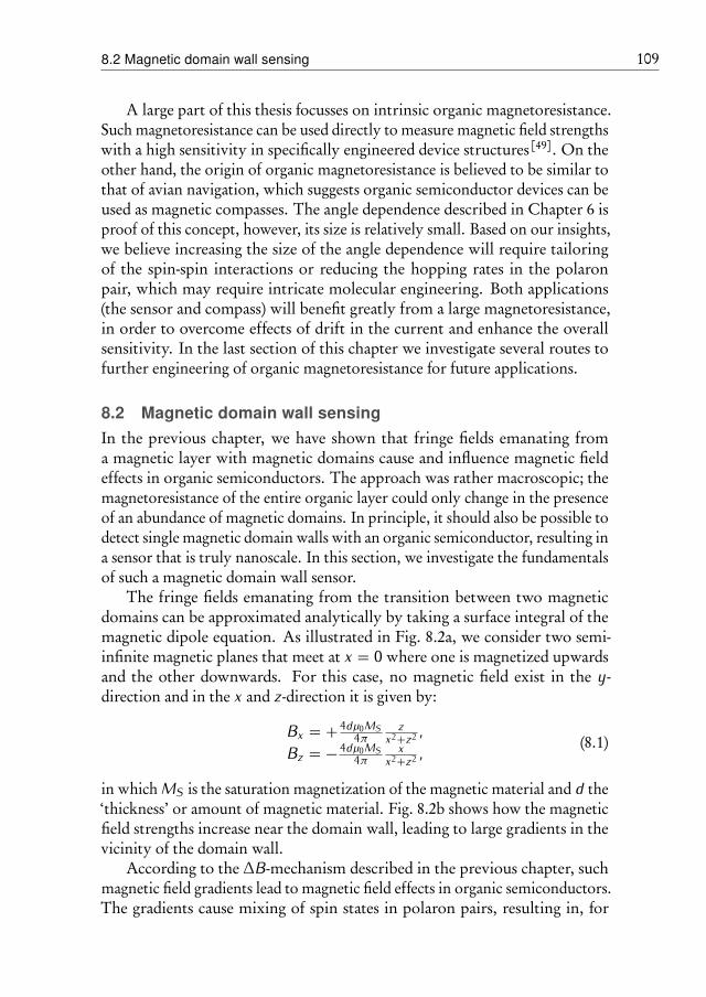
8.2 Magnetic domain wall sensing 109
A large part of this thesis focusses on intrinsic organic magnetoresistance.Such magnetoresistance can be used directly to measure magnetic field strengthswith a high sensitivity in specifically engineered device structures[49]. On theother hand, the origin of organic magnetoresistance is believed to be similar tothat of avian navigation, which suggests organic semiconductor devices can beused as magnetic compasses. The angle dependence described in Chapter 6 isproof of this concept, however, its size is relatively small. Based on our insights,we believe increasing the size of the angle dependence will require tailoringof the spin-spin interactions or reducing the hopping rates in the polaronpair, which may require intricate molecular engineering. Both applications(the sensor and compass) will benefit greatly from a large magnetoresistance,in order to overcome effects of drift in the current and enhance the overallsensitivity. In the last section of this chapter we investigate several routes tofurther engineering of organic magnetoresistance for future applications.
8.2 Magnetic domain wall sensing
In the previous chapter, we have shown that fringe fields emanating froma magnetic layer with magnetic domains cause and influence magnetic fieldeffects in organic semiconductors. The approach was rather macroscopic; themagnetoresistance of the entire organic layer could only change in the presenceof an abundance of magnetic domains. In principle, it should also be possible todetect single magnetic domain walls with an organic semiconductor, resulting ina sensor that is truly nanoscale. In this section, we investigate the fundamentalsof such a magnetic domain wall sensor.
The fringe fields emanating from the transition between two magneticdomains can be approximated analytically by taking a surface integral of themagnetic dipole equation. As illustrated in Fig. 8.2a, we consider two semi-infinite magnetic planes that meet at x = 0 where one is magnetized upwardsand the other downwards. For this case, no magnetic field exist in the y-direction and in the x and z-direction it is given by:
Bx = +4dµ0MS4π zx2+z2 ,
Bz = −4dµ0MS4π xx2+z2 , (8.1)
in whichMS is the saturation magnetization of the magnetic material and d the‘thickness’ or amount of magnetic material. Fig. 8.2b shows how the magneticfield strengths increase near the domain wall, leading to large gradients in thevicinity of the domain wall.
According to the ∆B-mechanism described in the previous chapter, suchmagnetic field gradients lead to magnetic field effects in organic semiconductors.The gradients cause mixing of spin states in polaron pairs, resulting in, for
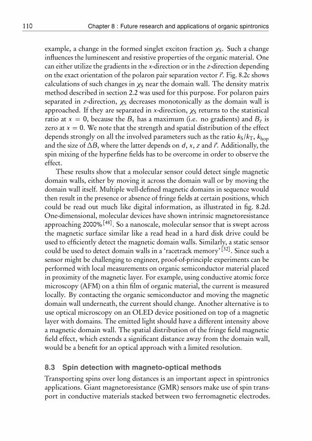
110 Chapter 8 : Future research and applications of organic spintronics
example, a change in the formed singlet exciton fraction χS. Such a changeinfluences the luminescent and resistive properties of the organic material. Onecan either utilize the gradients in the x-direction or in the z-direction dependingon the exact orientation of the polaron pair separation vector ~r. Fig. 8.2c showscalculations of such changes in χS near the domain wall. The density matrixmethod described in section 2.2 was used for this purpose. For polaron pairsseparated in z-direction, χS decreases monotonically as the domain wall isapproached. If they are separated in x-direction, χS returns to the statisticalratio at x = 0, because the Bx has a maximum (i.e. no gradients) and Bz iszero at x = 0. We note that the strength and spatial distribution of the effectdepends strongly on all the involved parameters such as the ratio kS/kT, khopand the size of ∆B, where the latter depends on d, x, z and ~r. Additionally, thespin mixing of the hyperfine fields has to be overcome in order to observe theeffect.
These results show that a molecular sensor could detect single magneticdomain walls, either by moving it across the domain wall or by moving thedomain wall itself. Multiple well-defined magnetic domains in sequence wouldthen result in the presence or absence of fringe fields at certain positions, whichcould be read out much like digital information, as illustrated in fig. 8.2d.One-dimensional, molecular devices have shown intrinsic magnetoresistanceapproaching 2000%[48]. So a nanoscale, molecular sensor that is swept acrossthe magnetic surface similar like a read head in a hard disk drive could beused to efficiently detect the magnetic domain walls. Similarly, a static sensorcould be used to detect domain walls in a ‘racetrack memory’[32]. Since such asensor might be challenging to engineer, proof-of-principle experiments can beperformed with local measurements on organic semiconductor material placedin proximity of the magnetic layer. For example, using conductive atomic forcemicroscopy (AFM) on a thin film of organic material, the current is measuredlocally. By contacting the organic semiconductor and moving the magneticdomain wall underneath, the current should change. Another alternative is touse optical microscopy on an OLED device positioned on top of a magneticlayer with domains. The emitted light should have a different intensity abovea magnetic domain wall. The spatial distribution of the fringe field magneticfield effect, which extends a significant distance away from the domain wall,would be a benefit for an optical approach with a limited resolution.
8.3 Spin detection with magneto-optical methods
Transporting spins over long distances is an important aspect in spintronicsapplications. Giant magnetoresistance (GMR) sensors make use of spin trans-port in conductive materials stacked between two ferromagnetic electrodes.
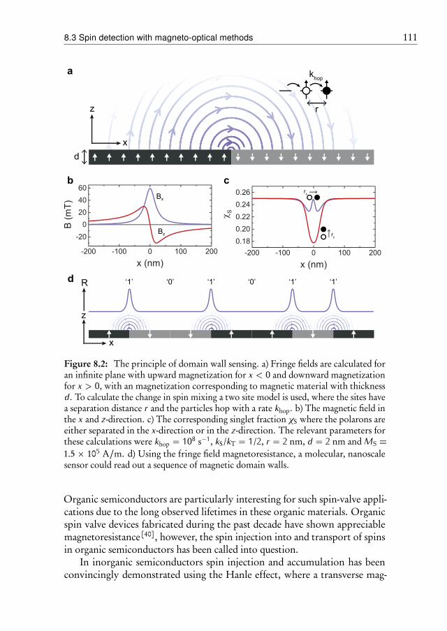
8.3 Spin detection with magneto-optical methods 111
‘1’ ‘0’ ‘1’ ‘0’ ‘1’ ‘1’
d
x
z
khop
r
Bx
Bz rz
rx
a
b c
d
x
z
R
Figure 8.2: The principle of domain wall sensing. a) Fringe fields are calculated foran infinite plane with upward magnetization for x < 0 and downward magnetizationfor x > 0, with an magnetization corresponding to magnetic material with thicknessd. To calculate the change in spin mixing a two site model is used, where the sites havea separation distance r and the particles hop with a rate khop. b) The magnetic field inthe x and z-direction. c) The corresponding singlet fraction χS where the polarons areeither separated in the x-direction or in the z-direction. The relevant parameters forthese calculations were khop = 108 s−1, kS/kT = 1/2, r = 2 nm, d = 2 nm and MS =1.5 × 10⁵ A/m. d) Using the fringe field magnetoresistance, a molecular, nanoscalesensor could read out a sequence of magnetic domain walls.
Organic semiconductors are particularly interesting for such spin-valve appli-cations due to the long observed lifetimes in these organic materials. Organicspin valve devices fabricated during the past decade have shown appreciablemagnetoresistance[40], however, the spin injection into and transport of spinsin organic semiconductors has been called into question.
In inorganic semiconductors spin injection and accumulation has beenconvincingly demonstrated using the Hanle effect, where a transverse mag-
112 Chapter 8 : Future research and applications of organic spintronics
netic field induces spin precession and thereby strongly affects the device resis-tance[189–192]. However, the absence of the Hanle effect in organic spin-valvestructures has cast doubts on the spin injection and transport in organic semi-conductors [187]. On the other hand, muon spin rotation measurements [43],two-photon photoemission experiments [42] and spin polarized tunneling intoa superconductor[193] indicate spin injection is feasible.
Another approach may be called for to effectively detect spin transport inorganic semiconductors. Besides the Hanle effect, one of the most convincingmethods for this purpose it to utilize magneto-optical techniques. With suchtechniques the polarization of the light can be linked to the spin states in amaterial, either through reflection, transmission or emission of such light. Forexample, spin-polarized currents have been detected in light emitting diodes bymeasuring the circular polarization of the emitted light[194].
Spin-polarized currents in organic semiconductors could be detected withmagneto-optical methods in two ways: (1) with the organic material itselfor (2) by inserting suitable materials such as quantum dots into the organicdevice. Unfortunately, these magneto-optical methods requires strong spin-orbit coupling, which is generally weak in organic materials, making thefirst option less viable. A solution to this problem would thus be to insertmaterials with a high spin-orbit coupling in the organic material, therebylocally measuring the spin-polarization. By fabricating devices with such spin-detecting layers at different locations, the spin-polarization can be tracked as afunction of the distance away from the spin-injecting electrode. Spin can beinjected and detected in inorganic quantum dots (QDs) [195–197]. Fabricationmethods already exist for hybrid organic QD devices, where the QDs can evenbe placed as a single layer at a fixed position within the device[198–200].
Several routes to use MO methods with QDs inside the organic device aredepicted schematically in Fig. 8.3. Electrically injected spins from a (single)ferromagnetic electrode will populate the QDs and can be detected in two ways.Either by detecting the circular polarization of spin-polarized electrons (holes)that recombine with unpolarized holes (electrons) inside the quantum dots,or by measuring the magneto-optical Kerr rotation from linearly polarizedlight reflected from the ensemble of QDs. We note that it is also possible toachieve the opposite of the first method: by irradiating the QDs with circularlypolarized light one can spin selectively excite carriers inside them, which arethen injected into the organic semiconductor.
Our own experiments have focussed on Cadmium Selenide (CdSe) quantumdots with a Zinc Sulfide (ZnS) shell. Such QDs can be inserted, for example,into a layer of the wide bandgap polymer polyfluorene to create hybrid LEDswith good light emitting properties[201]. We found that several bottleneckspresent themselves for the utilization of such devices for spin detection methods.
8.3 Spin detection with magneto-optical methods 113
a b c
NM
FM
QD
Figure 8.3: Possible routes to utilize magneto-optical (MO) methods in a non-magnetic (NM)/organic semiconductor/ferromagnet (FM) device structure with in-corporated high spin-orbit coupling materials (such as quantum dots (QDs)). a) Spin-polarized electrons injected from the FM electrode recombine with holes and emitcircularly polarized light. b) Spin-polarized electrons can be detected at the QDs withthe MO Kerr effect, via the rotation of linearly polarized light. c) Circularly polarizedlight can spin-selectively excite charge carriers, which are separated into the organicsemiconductor.
First of all, the QDs have a very strong electron affinity. Their low lying valenceband makes injection of holes from the polymer matrix into the QD virtuallyimpossible. Light emission from the QDs mainly takes place through energytransfer of excitons created in the organic layer. This means detection of circularpolarization of spin-polarized electrons that recombine with unpolarized holesinside the quantum dots, as illustrated in Fig. 8.3a, will not be achieved, becauseno direct recombination of electrons and holes takes place in the quantum dots.
We also investigated the spin lifetimes in the QDs with circularly polarizedphotoluminescence. With this technique one can spin selectively excite excitonsinside the QDs. When these excitons decay again without any spin dephasingthe same amount of circularly polarized light should be detected from the pho-toluminescence of the QDs. However, we observed no circularly polarizationin the photoluminescence at room temperature, which indicates complete spindephasing. This suggests QDs are not suitable for room temperature detectionand injection of spin-polarized currents in organic semiconductors.
As an alternative to quantum dots, one could use metal-organic complexes,which should exhibit higher spin-orbit coupling than general organic materials.On the other hand, Yu has shown with a first principles approach that the spin-orbit coupling in certain molecules, such as Alq3, might be higher than oneexpects from their elemental compound[74,140]. This suggests magneto-opticalmethods could already be applicable to such molecules. Shikoh et al. have takenthe first steps on this road, by demonstrating the emission of circular polarized
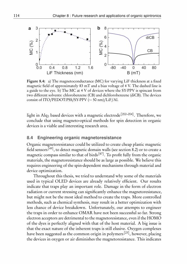
114 Chapter 8 : Future research and applications of organic spintronics
Figure 8.4: a) The magnetoconductance (MC) for varying LiF thickness at a fixedmagnetic field of approximately 83 mT and a bias voltage of 4 V. The dashed line isa guide to the eye. b) The MC at 4 V of devices where the SY-PPV is spincast fromtwo different solvents: chlorobenzene (CB) and dichlorobenzene (diCB). The devicesconsist of ITO/PEDOT:PSS/SY-PPV (∼ 50 nm)/LiF/Al.
light in Alq3 based devices with a magnetic electrode[202–204]. Therefore, weconclude that using magneto-optical methods for spin detection in organicdevices is a viable and interesting research area.
8.4 Engineering organic magnetoresistance
Organic magnetoresistance could be utilized to create cheap plastic magneticfield sensors[49], to detect magnetic domain walls (see section 8.2) or to create amagnetic compass similar to that of birds[87]. To profit fully from the organicmaterials, the magnetoresistance should be as large as possible. We believe thisrequires engineering of the spin-dependent mechanisms through material anddevice optimization.
Throughout this thesis, we tried to understand why some of the materialsused in typical OLED devices are already relatively efficient. Our resultsindicate that traps play an important role. Damage in the form of electronradiation or current stressing can significantly enhance the magnetoresistance,but might not be the most ideal method to create the traps. More controlledmethods, such as chemical synthesis, may result in a better optimization withless chance of device breakdown. Unfortunately, our attempts to engineerthe traps in order to enhance OMAR have not been successful so far. Strongelectron acceptors are detrimental to the magnetoresistance, even if the HOMOof the dyes is perfectly aligned with that of the host material. A big issue isthat the exact nature of the inherent traps is still elusive. Oxygen complexeshave been suggested as the common origin in polymers[23], however, placingthe devices in oxygen or air diminishes the magnetoresistance. This indicates
8.4 Engineering organic magnetoresistance 115
the traps responsible for the magnetoresistance are different in nature. Further(material) research is imperative in order to engineer organic magnetoresistancein cheap thin film structures.
So far little is known about how to engineer organic magnetoresistance byoptimizing the device structure. However, one can assume that the underlyingmechanisms will depend strongly on many parameters and processes (besidesthe traps), such as electron injection and morphology. In Fig. 8.4a we present apreliminary study of the effect of the electron injection on the MC magnitudeby varying the LiF thickness. LiF is a dusting layer in between the aluminumelectrode and the organic semiconductor and helps to overcome the largedifference in work function. In the investigated range, we found that a thickerLiF layer resulted in a higher luminescence efficiency. However, the MC ismaximized at rougly 0.5 nm, which suggests suboptimal electron injectionis beneficial for a large magnetic field sensitivity. As illustrated in Fig. 8.4b,another aspect in the fabrication process can significantly alter the MC. Bychanging the solvent from which the organic layer is spincoated, the MCincreases from 2.5% to more than 7%. Here the organic layer thickness is keptapproximately constant, as changes in thickness are known to influence theMC magnitude [205]. It could be that a different evaporation rate of the solventinduces a change in morphology and disorder, which influences many processesin the organic semiconductor. Clearly, besides material research, OMAR canalready be further enhanced by optimizing the device.
Another approach focussing on the device architecture was proposed byMahato et al., who were able to achieve 2000% magnetoresistance in organicdevices[48]. They focussed on confining the charge transport by insertingmolecules into the nanometer sized channels of a zeolite crystal, which resultsin organic wires of only one molecule thick. By placing the zeolites onto aconductive substrate and contacting it with a conductive AFM tip, the mag-netoresistance was measured. Due to the (probably) unipolar charge injectionand strong lateral confinement, the bipolaron mechanism is most likely at theorigin of this magnetoresistance. We should note that the authors also needtraps inside the channels to explain the magnitude of the magnetoresistance,so trap-related research seems unequivocally relevant for engineering magne-toresistance. The zeolite crystals are difficult to integrate into a functionaldevice, which is a disadvantage of the above approach. Other techniques tofabricate single molecule or nanometer sized channels are thus called for, suchas lithography or self-assembly.
We find that several routes present themselves for the engineering of largemagnetoresistance in organic semiconductors. First of all, the results in thisthesis have clearly shown that the spin-dependent processes can be influencedwith material engineering. We especially found the strong influence of traps on
116 Chapter 8 : Future research and applications of organic spintronics
the magnetoresistance. For example, in Chapter 4 these traps are deactivatedwith dopants and the magnetoresistance is completely quenched. Finding thephysical origin of these traps will result in viable strategies to chemically engi-neer the traps and strongly enhance organic magnetoresistance. Secondly, thedevice architecture can be optimized. We have briefly shown that straightfor-ward strategies targeting the electron injection at the electrodes or processing ofthe organic layer can have pronounced effects. Finally, reducing the dimension-ality of the system has been found to lead to huge magnetoresistance. Findingcheap and reliable methods to create similar 1D organic structures is anotherpromising research route. In conclusion, with many viable research strategiesahead we envision a bright future for engineering of organic magnetoresistance.
Summary
Magnetism and Molecular Materials
Investigating magnetic field effects in organic semiconductors
Organic semiconductors hold the promise to become the next generationof cheap, low-power electronics. By exploiting the role of spin in organicsemiconductors, the field of organic spintronics has added magnetic storageand magnetic field sensing applications to this promising class of materials.With recent reported values of over 2000% magnetoresistance at small field androom temperature, organic semiconductors now rank among the most sensitivematerials for the detection of magnetic fields. This might suggest cheap, plasticmagnetic field sensors are almost available on the market. However, severalobstacles block the route towards applications. The huge magnetoresistanceis only observed in complex devices produced with difficult and expensiveprocesses, while easy-to-process devices are still lacking in magnetoresistance.A fundamental knowledge of the physical processes underlying the magneticfield effects in organic semiconductors is required in order to create largemagnetoresistance in cheap devices.
From the research so far, several insights have already been gained. Mostimportantly, local hyperfine fields in the organic material seem to be involvedin the origin of the magnetic field effects. These hyperfine fields can causemixing, or intersystem crossing, of the spin states of particle pairs prior to aspin-dependent process, such as exciton formation from electron-hole pairs.The suppression of this spin mixing by an applied magnetic field is believed tobe responsible for the magnetic field effects. However, there is no consensusabout exactly which particles are involved, what reaction they undergo and howthe charge transport is influenced so dramatically. In this thesis we investigatethe magnetic field effects to analyse the underlying processes in greater detail inorder to move beyond the microscopic picture.
The experiments are performed on thin film devices, consisting of anorganic semiconductor sandwiched between (metal) electrodes. A wide range
117

118 Chapter 8 : Future research and applications of organic spintronics
of materials and material combinations is investigated, in order to elucidatethe underlying physical processes of the magnetic field effects. Our findingssuggest that traps in the semiconductor bandgap play an important role in themagnetic field effects. Additionally, we investigated novel functionalities forthe magnetoresistance, such as its angle dependence and ability to sense fringefields. The experiments primarily consist of detailed (magneto)resistance and(magneto)luminescence measurements. The experimental results are analysedwithin the framework of spin mixing mechanisms, as developed over the pastdecades for magnetic field dependent molecular reactions. Investigating suchmechanisms in organic semiconductors is relatively new and the influence ofdevice physics on the magnetic field effects has so far not been investigated. Forthis purpose, numerical finite element, drift-diffusion models of the deviceswere developed where the magnetic field effects are incorporated as changes inmaterial parameters or particle densities. We use these models to explain thevoltage dependence of the magnetoresistance and magneto-electroluminescence.
To explain the remarkable large magnetic field effects in organic light emit-ting devices, we developed a model which combines traps, triplet excitonsand the spin physics known to occur in organic semiconductors. The modelinvolves the spin dependent formation of triplet excitons at trap sites and theirsubsequent spin selective reaction with free polarons. We can show, with an-alytical and numerical calculations, that such a model is able to describe theexperimental magnetic field and bias voltage dependence of the magnetocon-ductance in several thin film OLEDs. In follow-up experimental studies, wehave tried to elucidate the exact role of traps with specialized molecular dopantsand chemically engineered polymers. We show that processes on the traps maybe solely responsible for the large magnetic field effects observed in the entiredevice.
The first of these experimental studies involved the doping of polymer thinfilm devices with an electron donor, to deactivate the initial electron traps, andwith an electron acceptor, to add additional electron traps. Deactivating theelectron traps led to a quenching of the magnetoresistance. However, dopingwith the electron acceptor also led to a reduction of the magnetoresistance.These results suggest that while the initial electron traps in the polymer lead toa large magnetoresistance, the traps induced by the electron acceptor do not,and competition of the latter with the initial traps leads to an eventual declineof the magnetoresistance.
In another study we investigated a polymer in which dye monomers can beinserted, which act as electron traps and recombination centres. Surprisingly,we found trap-assisted radiation in the backbone polymer itself. By investi-gating the spectrum of the magnetoelectroluminescence, we found that theluminescence at the trap sites has an opposite response to a magnetic field with
8.4 Engineering organic magnetoresistance 119
respect to the backbone luminescence. Together with numerical modelling,these results indicate that spin mixing at the traps can create the large magneticfield effects observed on the backbone. The added dyes that act as electrontraps reduced the magnetoresistance, but also showed an opposite magnetoelec-troluminescence as the initial traps, which indicates that their spin physics isdifferent from the initial traps. Clearly, more molecular engineering is requiredto find dopants or dyes that enhance the magnetoresistance.
Furthermore, it is known that magnetic field effects depend on the anglebetween the device normal and the applied magnetic field, which means such or-ganic semiconductors could be used as a magnetic compass. However, the exactorigin of this anisotropy was still unknown. We investigated the anisotropy ofthe magnetoconductance in a super yellow PPV polymer device. The shape ofthe found angle dependence at low magnetic fields strongly suggest that dipolarcoupling between polaron spins plays an important role in the anisotropy ofthe magnetic field effects. We also found a high field effect anisotropy, whichcould not be accurately explained with contemporary models.
In another approach, we investigated the influence of gradients in a magneticfield on the magnetic field effects. This was done by placing the organicsemiconductor on a magnetic layer in which magnetic domains can be created.When magnetic domains are present, fringe fields emanating from this layer canlead to strong field gradients. This can significantly change the magnetic fieldeffects. The fringe field effects reduce strongly with distance, which correlateswith the decay of the gradients over distance. We find that such fringe fieldmagnetic field effects can be analysed with a so called ∆B-mechanism, wherespin mixing occurs due to differences in magnetic field amplitude at adjacentmolecular sites.
We proposed several routes for future research and applications of organicspintronics. With the ∆B-mechanism, we have shown that nanoscale organicsensors could detect single magnetic domain walls. Additionally, we proposednew methods to detect spin-polarized currents in organic semiconductors. Fi-nally, based on the knowledge gained from our research into intrinsic magneticfield effects, we provide future researchers with a guide to further engineerorganic magnetoresistance.

Samenvatting
Magnetisme and Moleculaire Materialen
Onderzoek naar magneetveldeffecten in organische halfgeleiders
Organische halfgeleiders zijn veelbelovende materialen voor de nieuwe gen-eratie van goedkope elektronica met een laag energieverbruik. Naast het ge-bruik van lading voor elektronische toepassingen, probeert het onderzoeksveldorganische spintronica ook de spin van elektronen te gebruiken in organis-che halfgeleiders. Dit maakt het mogelijk om applicaties omtrent magnetis-che dataopslag en magneetvelddetectie toe te voegen aan het potentieel vandeze organische materialen. Het lijkt er tegenwoordig zelfs op dat organis-che halfgeleiders tot de meest gevoelige materialen behoren voor het metenvan magnetische velden, want in de literatuur zijn gigantische magnetoweer-standswaardes van meer dan 2000% gerapporteerd bij kamertemperatuur enkleine magnetische velden. Deze ontwikkelingen suggereren wellicht dat goed-kope, plastic magnetometers binnenkort commercieel verkrijgbaar zijn. Erzijn echter verschillende obstakels die deze toepassing nog in de weg staan.De enorme magnetoweerstandswaardes zijn enkel waargenomen in organis-che toepassingen met een complexe structuur en bijbehorende dure fabricage,terwijl eenvoudig te fabriceren organische toepassingen tot nu toe mindergevoelig blijken voor magnetische velden. Om grotere magnetoweerstanden teontwikkelen in goedkope organische toepassingen is een fundamentele kennisvan de onderliggende fysische processen van groot belang.
Wetenschappelijk onderzoek heeft tot nu toe al verschillende inzichtenopgeleverd. Het blijkt bijvoorbeeld dat hyperfijnvelden zeer belangrijk zijnvoor het veroorzaken van de magneetveldeffecten in organische halfgeleiders.Deze hyperfijnvelden zijn een soort lokale, willekeurige magneetvelden diedoor het organische materiaal zelf worden gecreëerd en randomiseren (of mixen)de spintoestanden van deeltjesparen voordat ze een spinafhankelijke reactieondergaan, zoals excitonvorming vanuit een elektron en een gat. Een extern
121
122 Chapter 8 : Future research and applications of organic spintronics
magnetisch veld onderdrukt deze randomisatie en kan daarmee de reactiesbeïnvloeden, wat tot de magneetveldeffecten leidt. Het is echter nog steedsniet duidelijk welke deeltjes precies een rol spelen, welke spinafhankelijkereacties ze ondergaan en hoe deze de stroom en ladingstransport door deorganische halfgeleider zo sterk beïnvloeden. In deze dissertatie hebben we demagneetveldeffecten beter bekeken om de uit te vinden wat de onderliggendeoorzaak nu precies is en hoe we ze kunnen verbeteren.
De experimenten zijn uitgevoerd op organische halfgeleiders die zijn gefab-riceerd met dunne-filmtechnologie, waarbij de organische halfgeleider tussentwee (metalen) elektrodes is geplaatst. Een grote hoeveelheid materialen enmateriaalcombinaties is onderzocht om de onderliggende fysische processenbeter te begrijpen. Onze resultaten wijzen erop dat ladingsvallen (Engels: traps)een grote rol spelen in de oorzaak van de magneetveldeffecten. Verder hebbenwe ook nieuwe functionaliteiten onderzocht, zoals de oriëntatieafhankelijkheidvan de magnetoweerstand en de mogelijkheid om gradiënten in het magneetveldte detecteren. Al deze resultaten zijn geanalyseerd met de spinrandomisatiemechanismen, die de afgelopen decennia zijn ontwikkeld voor magnetisch-veldafhankelijke moleculaire reacties. De toepassing van zulke mechanismen oporganische halfgeleiders is relatief nieuw en vooral de invloed van ladingstrans-port is onbekend. Daarom hebben we numerieke modellen ontwikkeld voorde ladingstransport, waar de magneetveldeffecten worden gesimuleerd metveranderingen in materiaalparameters of deeltjesdichtheden. Deze modellenkunnen we gebruiken om bijvoorbeeld de spanningsafhankelijkheid van demagnetoweerstand en magnetoluminescentie te begrijpen.
Om de relatief grote magneetveldeffecten in organische lichtgevende diodes(OLEDs) te verklaren, hebben we een model ontwikkeld dat de kennis omtrentladingsvallen, excitonen en spinfysica combineert. Het model omschrijft despinafhankelijke formatie van triplet excitonen in ladingsvallen en de spinse-lectieve reactie van deze triplet excitonen met vrije ladingen (polaronen). Metanalytische en numerieke berekeningen kunnen we laten zien dat dit modelde magnetisch-veldafhankelijkheid en spanningsafhankelijkheid van de magne-toweerstand in verschillende OLEDs goed beschrijft. In vervolgstudies hebbenwe de exact rol van de ladingsvallen beter bestudeerd, door middel van ma-teriaalonderzoek met gespecialiseerde moleculaire dotering en ontwikkeldepolymeren. Met deze studies kunnen we laten zien dat de processen op deladingsvallen de relatief grote magneetveldeffecten geheel kunnen verklaren.
In de eerste van deze studies doteerden we dunne-film, polymeren lagenmet enerzijds een elektronenacceptor en anderzijds met een elektronendonor.De elektronendonor deactiveert de ladingsvallen en onze resultaten laten ziendat de magnetoweerstand hiermee wordt uitgeschakeld. De lagen doteren meteen elektronenacceptor leidt tot meer ladingsvallen, maar leidt ook tot een ver-
8.4 Engineering organic magnetoresistance 123
mindering van de magnetoweerstand. Deze studie laat zien dat de ladingsvallendie initieel in de polymeren laag aanwezig zijn tot de magnetoweerstand leiden,maar dat de elektronenacceptoren niet dezelfde spinfysica omvatten, en datcompetitie tussen deze nieuwe ladingsvallen en de initiële ladingsvallen tot eenvermindering van de magnetoweerstand kan leiden.
In een opvolgende studie hebben we een polymeer bestudeerd waar monomerenin geplaatst kunnen worden die als ladingsval en recombinatiecentrum fungeren.Opmerkelijk genoeg vonden we al recombinatie in de ladingsvallen van hetinitiële polymeer. Door het spectrum van de magneto-elektroluminescentie teonderzoeken, vonden we dat de luminescentie van de ladingsvallen tegengesteldreageert op een magnetisch veld als de luminescentie van het polymeer zelf.Samen met de resultaten van numerieke modellen, kunnen we nu aantonendat spinrandomisatie op de ladingsvallen de geobserveerde magneetveldeffectenop het polymeer veroorzaakt. De toevoegde monomeren, die als ladingsvallenfungeren, verminderen de magnetoweerstand, maar laten ook een tegengesteldemagneto-elektroluminescentie zien als de initiële ladingsvallen op het polymeer.Dit suggereert dat hun spinfysica anders is dan die op de initiële ladingsvallenplaats vind. Het is duidelijk dat meer onderzoek nodig is naar moleculen ofmonomeren die zowel als ladingsval fungeren en de magnetoweerstand ver-hogen.
Naast deze studies hebben we onderzoek gedaan naar de afhankelijkheidvan de oriëntatie van het magneetveld ten opzichte van de organische laagop de magnetoweerstand. Het is bekend dat er een oriëntatieafhankelijkheidbestaat, wat nuttig is voor het ontwikkelen van een organisch kompas, maar deexacte oorsprong van deze anisotropie was onbekend. Wij hebben onderzoekgedaan naar de anisotropie van de magnetoweerstand in ’super yellow’ poly(p-phenylene vinylene) polymeren lagen. De vorm van de oriëntatieafhanke-lijkheid suggereert dat bij kleine magnetische velden de dipool-dipool kop-peling tussen de ladingsdragers een grote rol speelt in het veroorzaken vande anisotropie. Verder vonden we ook een anisotropie bij hoge magnetischevelden, die we niet goed konden verklaren met de huidige modellen.
We hebben ook onderzoek gedaan naar de invloed van gradiënten in hetmagneetveld op de magneetveldeffecten. Dit kan door een organische halfgelei-der op een magnetische laag te plaatsen waarin magnetische domeinen wordengecreëerd. Wanneer de magnetische domeinen aanwezig zijn, ontstaan er mag-netische randvelden vanuit de magnetische laag met sterke gradiënten, wat demagneetveldeffecten significant beïnvloed. De ontstane ’randveldmagneetveld-effecten’ verminderen snel als de afstand tussen de magnetische laag en deorganische laag wordt vergroot, wat overeenkomt met een vermindering vande gedetecteerde gradiënten in de organische laag. Zulke randveldmagneetveld-effecten kunnen goed beschreven worden met het zo door ons genoemde
124 Chapter 8 : Future research and applications of organic spintronics
∆B-mechanisme, waarmee spinrandomisatie wordt beschreven onder invloedvan verschillende magneetveldsterktes op verschillende locaties.
In een laatste hoofdstuk beschrijven we verschillende mogelijkheden voortoekomstig onderzoek en toepassingen van organische spintronica. Met be-hulp van het ∆B-mechanisme, kunnen we laten zien dat moleculaire sensorengebruikt kunnen worden om magnetische domeinmuren te detecteren, watinteressant is voor nieuwe geheugenelementen. Daarnaast stellen we nieuwemethoden voor om spin-gepolariseerde stromen te detecteren in organischehalfgeleiders. Als laatste leveren we met de opgedane kennis in deze dissertatieduidelijk advies aan toekomstige onderzoekers om organische magnetoweer-stand verder door te ontwikkelen.
Curriculum vitae
Matthijs Cox was born on October 24, 1986 in Valkenswaard. After finishinghigh school in 2005 at the SG Weredi College in Valkenswaard, he studiedApplied Physics at the Eindhoven University of Technology.
For his studies he did a minorproject in the group Catalysis and Energyof prof.dr. P.H.L Notten on hydrogen storage in metal hydrides, a localintership in the group Elementary Processes in Gas Dicharges of prof.dr.ir.G.M.W. Kroesen on dust formation in plasmas and an external traineeshipat FEI company in Acht on novel CMOS sensors for transmission electronmicroscopy. His graduation project was carried out in the group Physics ofNanostructures (FNA) of prof.dr. B. Koopmans. The research was done inthe field of organic spintronics on magnetic field effects in polymer-fullereneblends. The results were published and he obtained his Master degree cumlaude in 2010.
After his graduation he decided to continue the research on organic spin-tronics at FNA as a PhD candidate. Part of his PhD work is presented inthis dissertation, in several scientific journals and at international conferences.Besides with his colleagues at FNA, he collaborated with researchers from thegroup Molecular Materials and Nanosystems, the group Theory of Polymersand Soft matter as well as with researchers from the Groningen Universityand the University of Antwerp. As part of his work, Matthijs supervised twoBachelor and one Master student, and two external trainees. He was chosenas best practicum supervisor of the physics department in 2011. He also wonthe poster prize at the 11th European Conference on Molecular Engineering in2011 and the oral presentation prize at the NWOnano day in 2014.
During his PhD, Matthijs became a board member of the alumni associa-tion of Applied Physics (VENI), where he was responsible for the quarterlymagazine (N!). Through his editorial work he gained an interest in digitalgraphical design. One of his designs was on the cover of MRS Bulletin.
125

List of publications
Spectroscopic evidence for trap-dominated magnetic field effects in or-ganic semiconductors, M. Cox, M. H. A. Wijnen, G. A. H. Wetzelaer, M.Kemerink, P. W. M. Blom, and B. Koopmans, Physical Review B 90, 155205(2014).
Understanding Triplet Formation Pathways in Bulk Heterojunction Poly-mer:Fullerene Photovoltaic Devices, B. Z. Tedlla, F. Zhu, M. Cox, J. Drij-koningen, J. Manca, B. Koopmans, and E. Goovaerts, Advanced Energy Materi-als, advanced online publication (2014).
Anisotropic magnetoconductance in polymer thin films, M. Cox, J. M.Veerhoek, F. Zhu, and B. Koopmans, Physical Review B 89, 195204 (2014).
Investigating the influence of traps on organic magnetoresistance bymolecular doping, M. Cox, E. H. M. van der Heijden, P. Janssen, and B.Koopmans, Physical Review B 89, 085201 (2014).
The influence of the triplet exciton and charge transfer state energyalignment on organic magnetoresistance, P. Janssen, S. H. W. Wouters,M. Cox, and B. Koopmans, Organic Electronics 15, 743 (2014).
Tuning organic magnetoresistance in polymer-fullerene blends by con-trolling spin reaction pathways, P. Janssen, M. Cox, S. H. W. Wouters, M.Kemerink, M. M. Wienk, and B. Koopmans, Nature communications 4, 2286(2013).
Traps and trions as origin of magnetoresistance in organic semicon-ductors, M. Cox, P. Janssen, F. Zhu, and B. Koopmans, Physical Review B 88,035202 (2013).
127
128 Chapter 8 : Future research and applications of organic spintronics
The influence of device physics on organic magnetoresistance, M. Cox,P. Janssen, S. H. W. Wouters, E. H. M. van der Heijden, M. Kemerink, M. M.Wienk and B. Koopmans, Synthetic Metals 173, 10-15 (2013).
Large magnetic field effects in electrochemically doped organic light-emitting diodes, S. van Reenen, S. P. Kersten, S. H. W. Wouters, M. Cox, P.Janssen, B. Koopmans, P. A. Bobbert, and M. Kemerink, Physical Review B 88,125203 (2013).
Unraveling the temperature and voltage dependence of magnetic fieldeffects in organic semiconductors, P. Janssen, S. H. W. Wouters, M. Cox,and B. Koopmans, Journal of Applied Physics 114, 174909 (2013).
∆B-mechanism for fringe field organic magnetoresistance, M. Cox, S. P.Kersten, J. M. Veerhoek, P. Bobbert, and B. Koopmans, Manuscript submittedto Physical Review B.
Spin Dependent Photophysics in Lightly Fullerene Doped Polymers: In-vestigation by Photoluminescence- and Electrically-Detected MagneticResonance Techniques, B. Z. Tedlla, F. Zhu, M. Cox, B. Koopmans, and E.Goovaerts, Manuscript submitted to Physical Review B.
Acknowledgements / Dankwoord
Het dankwoord. Hier mag ik iedereen bedanken die mij tijdens mijn promotieheeft geholpen en hoef ik mijn gedachten eens niet in een wetenschappelijkkeurslijf te dwingen. In ieder geval bedank ik jou alvast, omdat je mijn proef-schrift hebt bekeken, open hebt geslagen en de moeite neemt om iets ervan telezen.
Ten eerste bedank ik hier mijn promotor en directe begeleider: Bert Koop-mans. Jouw energie en enthousiasme zijn altijd erg aanstekelijk en hebbenbijgedragen aan mijn keuze om toch ‘eventjes’ een promotie te doen. Ik magjou dus ook bedanken voor al die keren dat ik ’s nachts wakker heb gelegen,nog steeds bezig met de fysica van organische spintronica. Hoe je met je bizardrukke werkschema toch tijd kunt vinden voor je promovendi en studenten iseigenlijk onbegrijpelijk, maar jouw begeleiding zal voor mij altijd dienen alsinspiratie.
Daarna is het de beurt aan Henk Swagten, mijn tweede promotor. Eigenlijkweet je niet zo veel van organische halfgeleiders, maar je hebt me veel geholpenmet je commentaar op mijn presentaties, om mijn boodschap beter over tebrengen en mijn (soms) chaotische verhalen te structuren. Dus bij dezen:bedankt voor al je commentaar op mijn gedrag en bevindingen, niet iedereenzou dat kunnen waarderen, maar mij heeft het zeker geholpen.
Derde in het lijstje is mijn copromotor Stefan Meskers. Het project waarmijn promotie om zou moeten draaien is helaas niet zo succesvol geblekenen daardoor is jouw invloed op mijn promotie minder groot geweest dan weoorspronkelijk dachten. Toch bedankt voor je bevlogenheid met natuurkundeen chemie en de uren in het lab waar we knoeiden met circulair gepolariseerdlicht.
I would like to thank all other members of my PhD committee for carefullyanalysing my thesis and discussing points of improvement. Thank you NeilGreenham, Markus Wohlgenannt, Wilfred van der Wiel and Peter Bobbert.Peter ook bedankt voor alle discussies tijdens conferenties.
129
130 Chapter 8 : Future research and applications of organic spintronics
Verder zijn er nog de twee Martijnen van de vakgroep M2N die mij metveel raad en daad hebben bijgestaan. Martijn Wienk, bedankt dat ik je altijdlastig mocht vallen met mijn nieuwe ideeën. Ondanks dat ze soms niet duidelijkwaren, kon je me toch altijd advies geven over materialen en meetmethoden.Martijn Kemerink, bedankt voor je expertise over organische halfgeleiders enje hulp bij het inbouwen van de spinfysica in DriftKicker.
Zelfs met al het advies van alle bovenstaande academici is in je eentje werkenaan organische spintronica maar een saaie bedoeling, dus daarom bedank ikgraag alle leden van de ‘organics crew’ voor de fijne samenwerking. Paul, jewas mijn begeleider tijdens de master en directe collega tijdens de promotie.Bedankt voor je gezelligheid in het lab en tijdens discussies en vergeet vooralonze gezamenlijke avonturen op conferenties niet. Jürgen, bedankt voor alje expertise. Thank you Feng Zhu, for your positive energy and showing mepersonally that Chinese people can be really crazy and extravert. Bij de organicscrew horen ook alle studenten die ik direct of indirect begeleidt heb. Marcel,Ilse, Steinar, Irene, Mark, Melanie en Luuk, bedankt voor al jullie inzet en devele resultaten die hier in mijn proefschrift beschreven staan.
Naast de leden van de ‘organics crew’ heb ik ook schouder aan schouder inhet lab gestaan met de vele leden van de vakgroep Fysica van Nanostructuren.Reinoud, Sjors, Jeroen, Aurelie, Koen en de vele anderen die ik heb mogenontmoeten, bedankt voor de fijne tijd en jullie hulp met experimentele op-stellingen die ik zelf niet helemaal begreep. Thank you Nidhi, for sharing myoffice for so long and introducing me to the Indian culture. De vakgroep zouook allang vastgelopen zijn zonder de technische ondersteuning van Gerrie enJeroen. Karin, bedankt voor je luisterend oor en al je hulp bij administratieveproblemen. Er bestaan ook vele mensen die ik lastig heb gevallen op de univer-siteit, conferenties en vele andere gelegenheden, te veel om bij naam te noemen.Iedereen bedankt voor jullie hulp en gezelligheid.
Buiten werktijd is de steun van vrienden en familie ontzettend belangrijk.Extra veel dank aan mijn ouders en zusje, vele jaren geleden zijn we Bastiaanhelaas verloren, maar we zijn er altijd voor elkaar geweest en ik denk dat we ersterker uit naar voren zijn gekomen. Dat helpt mij om door te zetten als hettegenzit, ook tijdens de promotie.
Sonja, van jou krijg ik altijd een dagelijkse portie liefde en een extra dosisassertiviteit. Bedankt voor alles wat we samen al hebben beleefd, de fijne enmindere fijne momenten. Tijdens de achtbaan die mijn promotie heette, zijnwe ook nog eens getrouwd en ouders geworden van onze prachtige zoon. Endaarmee kom ik ten slotte bij jou; Floris, bedankt voor jouw vreugde en dat jeme motiveert om meer uit mezelf te halen.
Bibliography
[1] S. R. Forrest, The path to ubiquitous and low-cost organic electronic applianceson plastic, Nature 428, 911 (2004).
[2] H. Mette and H. Pick, Elektronenleitfahigkeit von anthracen-einkristallen., Z.Phys. 134, 566 (1953).
[3] H. Akamatu, H. Inokuchi, and Y. Matsunaga, Electrical conductivity of theperylene-bromine complex, Nature 173, 168 (1954).
[4] C. K. Chiang, C. R. Fincher, Y. W. Park, A. J. Heeger, H. Shirakawa, E. J.Louis, S. C. Gau, and A. G. Macdiarmid, Electrical conductivity in dopedpolyacetylene, Phys. Rev. Lett. 39, 1098 (1977).
[5] C. W. Tang and S. A. VanSlyke, Organic electroluminescent diodes, Appl. Phys.Lett. 51, 913 (1987).
[6] J. H. Burroughes, D. D. C. Bradley, R. N. Marks, K. Mackay, R. H. Friend,P. L. Burns, and A. B. Holmes, Light-emitting diodes based on conjugatedpolymers, Nature 347, 539 (1990).
[7] C. W. Tang, Two-layer organic photovoltaic cell, Appl. Phys. Lett. 48, 183(1986).
[8] G. Yu, J. Gao, J. C. Hummelen, F. Wudl, and A. J. Heeger, Polymer Photo-voltaic Cells: Enhanced Efficiencies via a Network of Internal Donor-AcceptorHeterojunctions, Science 270, 1789 (1995).
[9] H. Klauk, Organic thin-film transistors, Chem. Soc. Rev. 39, 2643 (2010).
[10] R. Hoffmann, C. Janiak, and C. Kollmar, A chemical approach to the orbitalsof organic polymers, Macromolecules 24 (1991).
[11] H. Bässler, Charge Transport in Disordered Organic Photoconductors, Phys.Status Solidi B 175, 15 (1993).
[12] S. Stafström, Electron localization and the transition from adiabatic to nona-diabatic charge transport in organic conductors., Chem. Soc. Rev. 39, 2484(2010).
[13] E. M. Conwell, Impurity band conduction in germanium and silicon, Phys.Rev. 103, 51 (1956).
131
132 BIBLIOGRAPHY
[14] N. F. Mott, On the transition to metallic conduction in semiconductors, Can. J.Phys. 34, 1356 (1956).
[15] R. Coehoorn and P. A. Bobbert, Effects of Gaussian disorder on charge carriertransport and recombination in organic semiconductors, Phys. Status Solidi209, 2354 (2012).
[16] A. Miller and E. Abrahams, Impurity conduction at low concentrations, Phys.Rev. 257, 745 (1960).
[17] W. F. Pasveer, J. Cottaar, C. Tanase, R. Coehoorn, P. A. Bobbert, P. W. M.Blom, D. M. de Leeuw, and M. A. J. Michels, Unified Description of Charge-Carrier Mobilities in Disordered Semiconducting Polymers, Phys. Rev. Lett. 94,206601 (2005).
[18] M. P. Langevin, Recombinaison et mobilites des ions dans les gaz, Ann. Chim.Phys. 28, 433 (1903).
[19] J. J. M. van der Holst, F. W. A. van Oost, R. Coehoorn, and P. A. Bobbert,Electron-hole recombination in disordered organic semiconductors: Validity ofthe Langevin formula, Phys. Rev. B 80, 235202 (2009).
[20] P. W. M. Blom, M. J. M. de Jong, and S. Breedijk, Temperature dependentelectron-hole recombination in polymer light-emitting diodes, Appl. Phys. Lett.71, 930 (1997).
[21] P. W. M. Blom, M. J. M. de Jong, and J. J. M. Vleggaar, Electron and holetransport in poly(p-phenylene vinylene) devices, Appl. Phys. Lett. 68, 3308(1996).
[22] P. E. Burrows, Z. Shen, V. Bulovic, D. M. McCarty, S. R. Forrest, J. A.Cronin, and M. E. Thompson, Relationship between electroluminescence andcurrent transport in organic heterojunction light-emitting devices, J. Appl. Phys.79, 7991 (1996).
[23] H. T. Nicolai, M. Kuik, G. A. H. Wetzelaer, B. de Boer, C. Campbell,C. Risko, J. L. Brédas, and P. W. M. Blom, Unification of trap-limited electrontransport in semiconducting polymers., Nat. Mater. 11, 882 (2012).
[24] Y. Zhang, B. de Boer, and P. W. M. Blom, Trap-free electron transport in poly(p-phenylene vinylene) by deactivation of traps with n-type doping, Phys. Rev. B81, 085201 (2010).
[25] W. Graupner, G. Leditzky, G. Leising, and U. Scherf, Shallow and deep trapsin conjugated polymers of high intrachain order., Phys. Rev. B 54, 7610 (1996).
[26] M. Meier, S. Karg, K. Zuleeg, W. Brütting, and M. Schwoerer, Determinationof trapping parameters in poly(p-phenylenevinylene) light-emitting devices usingthermally stimulated currents, J. Appl. Phys. 84, 87 (1998).
[27] D. Y. Kondakov, J. R. Sandifer, C. W. Tang, and R. H. Young, Nonradiativerecombination centers and electrical aging of organic light-emitting diodes:Direct connection between accumulation of trapped charge and luminance loss,J. Appl. Phys. 93, 1108 (2003).
BIBLIOGRAPHY 133
[28] M. Kuik, L. J. A. Koster, G. A. H. Wetzelaer, and P. W. M. Blom, Trap-AssistedRecombination in Disordered Organic Semiconductors, Phys. Rev. Lett. 107,256805 (2011).
[29] H. T. Nicolai, A. Hof, and P. W. M. Blom, Device Physics of White PolymerLight-Emitting Diodes, Adv. Funct. Mater. 22, 2040 (2012).
[30] C. Chappert, A. Fert, and F. N. Van Dau, The emergence of spin electronics indata storage., Nat. Mater. 6, 813 (2007).
[31] D. D. Awschalom and M. E. Flatté, Challenges for semiconductor spintronics,Nat. Phys. 3, 153 (2007).
[32] S. S. P. Parkin, M. Hayashi, and L. Thomas, Magnetic domain-wall racetrackmemory., Science 320, 190 (2008).
[33] S. S. P. Parkin, K. P. Roche, M. G. Samant, P. M. Rice, R. B. Beyers, R. E.Scheuerlein, E. J. O’Sullivan, S. L. Brown, J. Bucchigano, D. W. Abraham,et al., Exchange-biased magnetic tunnel junctions and application to nonvolatilemagnetic random access memory, J. Appl. Phys. 85, 5828 (1999).
[34] P. P. Ruden and D. L. Smith, Theory of spin injection into conjugated organicsemiconductors, J. Appl. Phys. 95, 4898 (2004).
[35] S. Pramanik, C.-G. Stefanita, S. Patibandla, S. Bandyopadhyay, K. Garre,N. Harth, and M. Cahay, Observation of extremely long spin relaxation timesin an organic nanowire spin valve, Nat. Nanotechnol. 2, 216 (2007).
[36] D. R. McCamey, H. A. Seipel, S.-Y. Paik, M. J. Walter, N. J. Borys, J. M.Lupton, and C. Boehme, Spin Rabi flopping in the photocurrent of a polymerlight-emitting diode., Nat. Mater. 7, 723 (2008).
[37] T. D. Nguyen, G. Hukic-Markosian, F. Wang, L. Wojcik, X.-G. Li, E. Ehren-freund, and Z. V. Vardeny, Isotope effect in spin response ofπ-conjugated polymerfilms and devices., Nat. Mater. 9, 345 (2010).
[38] S. Watanabe, K. Ando, K. Kang, S. Mooser, Y. Vaynzof, H. Kurebayashi,E. Saitoh, and H. Sirringhaus, Polaron spin current transport in organic semi-conductors, Nat. Phys. 10, 308 (2014).
[39] V. Dediu, M. Murgia, F. C. Matacotta, C. Taliani, and S. Barbanera, Roomtemperature spin polarized injection in organic semiconductor, Solid State Com-mun. 122, 181 (2002).
[40] Z. H. Xiong, D. Wu, Z. V. Vardeny, and J. Shi, Giant magnetoresistance inorganic spin-valves, Nature 427, 821 (2004).
[41] J. J. H. M. Schoonus, P. G. E. Lumens, W. Wagemans, J. T. Kohlhepp, P. A.Bobbert, H. J. M. Swagten, and B. Koopmans, Magnetoresistance in HybridOrganic Spin Valves at the Onset of Multiple-Step Tunneling, Phys. Rev. Lett.103, 1 (2009).
[42] M. Cinchetti, K. Heimer, J.-P. Wüstenberg, O. Andreyev, M. Bauer, S. Lach,C. Ziegler, Y. Gao, and M. Aeschlimann, Determination of spin injection andtransport in a ferromagnet/organic semiconductor heterojunction by two-photonphotoemission., Nat. Mater. 8, 115 (2009).
134 BIBLIOGRAPHY
[43] A. J. Drew, J. Hoppler, L. Schulz, F. L. Pratt, P. Desai, P. Shakya, T. Kreouzis,W. P. Gillin, A. Suter, N. A. Morley, et al., Direct measurement of the electronicspin diffusion length in a fully functional organic spin valve by low-energy muonspin rotation., Nat. Mater. 8, 109 (2009).
[44] J.-W. Yoo, C.-Y. Chen, H. W. Jang, C. W. Bark, V. N. Prigodin, C. B. Eom,and A. J. Epstein, Spin injection/detection using an organic-based magneticsemiconductor., Nat. Mater. 9, 638 (2010).
[45] T. D. Nguyen, E. Ehrenfreund, and Z. V. Vardeny, Spin-polarized light-emitting diode based on an organic bipolar spin valve., Science 337, 204 (2012).
[46] Ö. Mermer, G. Veeraraghavan, T. L. Francis, Y. Sheng, T. D. Nguyen,M. Wohlgenannt, A. Köhler, M. K. Al-Suti, and M. S. Khan, Large mag-netoresistance in nonmagnetic π-conjugated semiconductor thin film devices,Phys. Rev. B 72, 205202 (2005).
[47] U. Niedermeier, M. Vieth, R. Pätzold, W. Sarfert, and H. von Seggern,Enhancement of organic magnetoresistance by electrical conditioning, Appl.Phys. Lett. 92, 193309 (2008).
[48] R. N. Mahato, H. Lülf, M. H. Siekman, S. P. Kersten, P. A. Bobbert, M. P.de Jong, L. De Cola, and W. G. van der Wiel, Ultrahigh magnetoresistance atroom temperature in molecular wires., Science 341, 257 (2013).
[49] W. J. Baker, K. Ambal, D. P. Waters, R. Baarda, H. Morishita, K. vanSchooten, D. R. McCamey, J. M. Lupton, and C. Boehme, Robust absolutemagnetometry with organic thin-film devices., Nat. Commun. 3, 898 (2012).
[50] F. Wang, F. Macià, M. Wohlgenannt, A. D. Kent, and M. E. Flatté, MagneticFringe-Field Control of Electronic Transport in an Organic Film, Phys. Rev. X2, 021013 (2012).
[51] N. Atodiresei, J. Brede, P. Lazic, V. Caciuc, G. Hoffmann, R. Wiesen-danger, and S. Blügel, Design of the Local Spin Polarization at the Organic-Ferromagnetic Interface, Phys. Rev. Lett. 105, 066601 (2010).
[52] L. Bogani and W. Wernsdorfer, Molecular spintronics using single-moleculemagnets., Nat. Mater. 7, 179 (2008).
[53] M. Urdampilleta, S. Klyatskaya, J.-P. Cleuziou, M. Ruben, and W. Wernsdor-fer, Supramolecular spin valves, Nat. Mater. 10, 502 (2011).
[54] K. V. Raman, A. M. Kamerbeek, A. Mukherjee, N. Atodiresei, T. K. Sen,P. Lazic, V. Caciuc, R. Michel, D. Stalke, S. K. Mandal, et al., Interface-engineered templates for molecular spin memory devices., Nature 493, 509(2013).
[55] S. Sanvito, Molecular spintronics: The rise of spinterface science, Nat. Phys. 6,562 (2010).
[56] R. C. Johnson, R. E. Merrifield, P. Avakian, and R. B. Flippen, Effects ofmagnetic fields on the mutual annihilation of triplet excitons in molecularcrystals, Phys. Rev. Lett. 19, 285 (1967).
BIBLIOGRAPHY 135
[57] N. Geacintov and M. Pope, Effect of magnetic field on the fluorescence oftetracene crystals: exciton fission, Phys. Rev. Lett. 22, 593 (1969).
[58] V. Ern and R. E. Merrifield, Magnetic field effect on triplet exciton quenchingin organic crystals, Phys. Rev. Lett. 21, 609 (1968).
[59] E. L. Frankevich and I. A. Sokolik, On the mechanism of the magnetic fieldeffect on anthracene photoconductivity, Solid State Commun. 8, 251 (1970).
[60] U. E. Steiner and T. Ulrich, Magnetic Field Effects in Chemical Kinetics andRelated Phenomena, Chem. Rev. 89, 51 (1989).
[61] B. Brocklehurst, Magnetic fields and radical reactions: recent developments andtheir role in nature, Chem. Soc. Rev. 31, 301 (2002).
[62] K. Schulten and P. G. Wolynes, Semiclassical description of electron spin motionin radicals including the effect of electron hopping, J. Chem. Phys. 68, 3292(1978).
[63] D. R. McCamey, K. J. van Schooten, W. J. Baker, S.-Y. Lee, S.-Y. Paik, J. M.Lupton, and C. Boehme, Hyperfine-Field-Mediated Spin Beating in Electrostati-cally Bound Charge Carrier Pairs, Phys. Rev. Lett. 104, 017601 (2010).
[64] S.-Y. Lee, S.-Y. Paik, D. R. Mccamey, J. Yu, P. L. Burn, J. M. Lupton, andC. Boehme, Tuning Hyperfine Fields in Conjugated Polymers for Coherent, J.Am. Chem. Soc. 133, 2019 (2011).
[65] A. J. Hoff, Magnetic field effects on photosynthetic reactions, Q. Rev. Biophys.14, 599 (1981).
[66] S. G. Boxer, C. E. D. Chidsey, and M. G. Roelofs, Magnetic Field Effects onReaction Yields in the Solid State: An Example from Photosynthetic ReactionCenters, Annu. Rev. Phys. Chem. 34, 389 (1983).
[67] T. Ritz, S. Adem, and K. Schulten, A model for photoreceptor-based magnetore-ception in birds., Biophys. J. 78, 707 (2000).
[68] K. Maeda, K. B. Henbest, F. Cintolesi, I. Kuprov, C. T. Rodgers, P. a. Liddell,D. Gust, C. R. Timmel, and P. J. Hore, Chemical compass model of avianmagnetoreception., Nature 453, 387 (2008).
[69] C. T. Rodgers and P. J. Hore, Chemical magnetoreception in birds: the radicalpair mechanism., Proc. Natl. Acad. Sci. U. S. A. 106, 353 (2009).
[70] E. L. Frankevich, A. A. Lymarev, I. Sokolik, F. E. Karasz, S. Blumsten-gel, R. H. Baughman, and H. H. Hörhold, Polaron-pair generation inpoly(phenylene vinylenes), Phys. Rev. B 46, 9320 (1992).
[71] J. Kalinowski, M. Cocchi, D. Virgili, P. Di Marco, and V. Fattori, Magneticfield effects on emission and current in Alq3-based electroluminescent diodes,Chem. Phys. Lett. 380, 710 (2003).
[72] T. L. Francis, Ö. Mermer, G. Veeraraghavan, and M. Wohlgenannt, Largemagnetoresistance at room temperature in semiconducting polymer sandwichdevices, New J. Phys. 6, 185 (2004).
[73] M. Cox, P. Janssen, S. H. W. Wouters, E. H. M. van der Heijden, M. Ke-
136 BIBLIOGRAPHY
merink, and B. Koopmans, The influence of device physics on organic magne-toresistance, Synth. Met. 173, 10 (2013).
[74] Z. Yu, Spin-orbit coupling and its effects in organic solids, Phys. Rev. B 85(2012).
[75] Z. G. Yu, F. Ding, and H. Wang, Hyperfine interaction and its effects on spindynamics in organic solids, Phys. Rev. B 87, 205446 (2013).
[76] N. J. Rolfe, M. Heeney, P. B. Wyatt, A. J. Drew, T. Kreouzis, and W. P. Gillin,Elucidating the role of hyperfine interactions on organic magnetoresistance usingdeuterated aluminium tris(8-hydroxyquinoline), Phys. Rev. B 80, 241201 (2009).
[77] N. J. Rolfe, M. Heeney, P. B. Wyatt, A. J. Drew, T. Kreouzis, and W. P. Gillin,The effect of deuteration on organic magnetoresistance, Synth. Met. 161, 608(2011).
[78] F. J. Wang, H. Bässler, and Z. Valy Vardeny, Magnetic Field Effects in π-Conjugated Polymer-Fullerene Blends: Evidence for Multiple Components, Phys.Rev. Lett. 101, 236805 (2008).
[79] B. R. Gautam, T. D. Nguyen, E. Ehrenfreund, and Z. V. Vardeny, Magneticfield effect on excited-state spectroscopies of π-conjugated polymer films, Phys.Rev. B 85, 205207 (2012).
[80] P. Janssen, M. Cox, S. H. W. Wouters, M. Kemerink, M. M. Wienk, andB. Koopmans, Tuning organic magnetoresistance in polymer-fullerene blends bycontrolling spin reaction pathways, Nat. Commun. 4, 2286 (2013).
[81] S. A. Bagnich, U. Niedermeier, C. Melzer, W. Sarfert, and H. von Seggern,Origin of magnetic field effect enhancement by electrical stress in organic lightemitting diodes, J. Appl. Phys. 105, 123706 (2009).
[82] F. L. Bloom, W. Wagemans, M. Kemerink, and B. Koopmans, Correspondenceof the sign change in organic magnetoresistance with the onset of bipolar chargetransport, Appl. Phys. Lett. 93, 263302 (2008).
[83] F. L. Bloom, W. Wagemans, M. Kemerink, and B. Koopmans, Separatingpositive and negative magnetoresistance in organic semiconductor devices, Phys.Rev. Lett. 99, 1 (2007).
[84] S. Zhang, A. J. Drew, T. Kreouzis, and W. P. Gillin, Modelling of organic mag-netoresistance as a function of temperature using the triplet polaron interaction,Synth. Met. 161, 628 (2011).
[85] P. Janssen, S. H. W. Wouters, M. Cox, and B. Koopmans, Unraveling thetemperature and voltage dependence of magnetic field effects in organic semicon-ductors, J. Appl. Phys. 114, 174909 (2013).
[86] W. Wagemans, A. J. Schellekens, M. Kemper, F. L. Bloom, P. A. Bobbert,and B. Koopmans, Spin-Spin Interactions in Organic Magnetoresistance Probedby Angle-Dependent Measurements, Phys. Rev. Lett. 106, 196802 (2011).
[87] T. D. Nguyen, E. Ehrenfreund, and Z. V. Vardeny, Organic magneto-resistanceat small magnetic fields; compass effect, Org. Electron. 14, 1852 (2013).
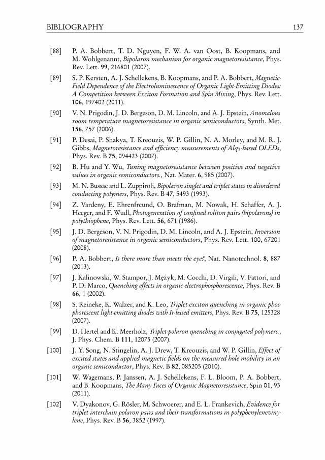
BIBLIOGRAPHY 137
[88] P. A. Bobbert, T. D. Nguyen, F. W. A. van Oost, B. Koopmans, andM. Wohlgenannt, Bipolaron mechanism for organic magnetoresistance, Phys.Rev. Lett. 99, 216801 (2007).
[89] S. P. Kersten, A. J. Schellekens, B. Koopmans, and P. A. Bobbert, Magnetic-Field Dependence of the Electroluminescence of Organic Light-Emitting Diodes:A Competition between Exciton Formation and Spin Mixing, Phys. Rev. Lett.106, 197402 (2011).
[90] V. N. Prigodin, J. D. Bergeson, D. M. Lincoln, and A. J. Epstein, Anomalousroom temperature magnetoresistance in organic semiconductors, Synth. Met.156, 757 (2006).
[91] P. Desai, P. Shakya, T. Kreouzis, W. P. Gillin, N. A. Morley, and M. R. J.Gibbs, Magnetoresistance and efficiency measurements of Alq3-based OLEDs,Phys. Rev. B 75, 094423 (2007).
[92] B. Hu and Y. Wu, Tuning magnetoresistance between positive and negativevalues in organic semiconductors., Nat. Mater. 6, 985 (2007).
[93] M. N. Bussac and L. Zuppiroli, Bipolaron singlet and triplet states in disorderedconducting polymers, Phys. Rev. B 47, 5493 (1993).
[94] Z. Vardeny, E. Ehrenfreund, O. Brafman, M. Nowak, H. Schaffer, A. J.Heeger, and F. Wudl, Photogeneration of confined soliton pairs (bipolarons) inpolythiophene, Phys. Rev. Lett. 56, 671 (1986).
[95] J. D. Bergeson, V. N. Prigodin, D. M. Lincoln, and A. J. Epstein, Inversionof magnetoresistance in organic semiconductors, Phys. Rev. Lett. 100, 67201(2008).
[96] P. A. Bobbert, Is there more than meets the eye?, Nat. Nanotechnol. 8, 887(2013).
[97] J. Kalinowski, W. Stampor, J. Mezyk, M. Cocchi, D. Virgili, V. Fattori, andP. Di Marco, Quenching effects in organic electrophosphorescence, Phys. Rev. B66, 1 (2002).
[98] S. Reineke, K. Walzer, and K. Leo, Triplet-exciton quenching in organic phos-phorescent light-emitting diodes with Ir-based emitters, Phys. Rev. B 75, 125328(2007).
[99] D. Hertel and K. Meerholz, Triplet-polaron quenching in conjugated polymers.,J. Phys. Chem. B 111, 12075 (2007).
[100] J. Y. Song, N. Stingelin, A. J. Drew, T. Kreouzis, and W. P. Gillin, Effect ofexcited states and applied magnetic fields on the measured hole mobility in anorganic semiconductor, Phys. Rev. B 82, 085205 (2010).
[101] W. Wagemans, P. Janssen, A. J. Schellekens, F. L. Bloom, P. A. Bobbert,and B. Koopmans, The Many Faces of Organic Magnetoresistance, Spin 01, 93(2011).
[102] V. Dyakonov, G. Rösler, M. Schwoerer, and E. L. Frankevich, Evidence fortriplet interchain polaron pairs and their transformations in polyphenyleneviny-lene, Phys. Rev. B 56, 3852 (1997).
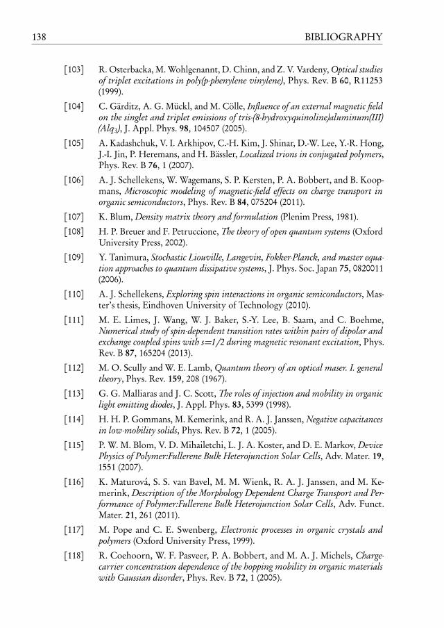
138 BIBLIOGRAPHY
[103] R. Osterbacka, M. Wohlgenannt, D. Chinn, and Z. V. Vardeny, Optical studiesof triplet excitations in poly(p-phenylene vinylene), Phys. Rev. B 60, R11253(1999).
[104] C. Gärditz, A. G. Mückl, and M. Cölle, Influence of an external magnetic fieldon the singlet and triplet emissions of tris-(8-hydroxyquinoline)aluminum(III)(Alq3), J. Appl. Phys. 98, 104507 (2005).
[105] A. Kadashchuk, V. I. Arkhipov, C.-H. Kim, J. Shinar, D.-W. Lee, Y.-R. Hong,J.-I. Jin, P. Heremans, and H. Bässler, Localized trions in conjugated polymers,Phys. Rev. B 76, 1 (2007).
[106] A. J. Schellekens, W. Wagemans, S. P. Kersten, P. A. Bobbert, and B. Koop-mans, Microscopic modeling of magnetic-field effects on charge transport inorganic semiconductors, Phys. Rev. B 84, 075204 (2011).
[107] K. Blum, Density matrix theory and formulation (Plenim Press, 1981).
[108] H. P. Breuer and F. Petruccione, The theory of open quantum systems (OxfordUniversity Press, 2002).
[109] Y. Tanimura, Stochastic Liouville, Langevin, Fokker-Planck, and master equa-tion approaches to quantum dissipative systems, J. Phys. Soc. Japan 75, 0820011(2006).
[110] A. J. Schellekens, Exploring spin interactions in organic semiconductors, Mas-ter’s thesis, Eindhoven University of Technology (2010).
[111] M. E. Limes, J. Wang, W. J. Baker, S.-Y. Lee, B. Saam, and C. Boehme,Numerical study of spin-dependent transition rates within pairs of dipolar andexchange coupled spins with s=1/2 during magnetic resonant excitation, Phys.Rev. B 87, 165204 (2013).
[112] M. O. Scully and W. E. Lamb, Quantum theory of an optical maser. I. generaltheory, Phys. Rev. 159, 208 (1967).
[113] G. G. Malliaras and J. C. Scott, The roles of injection and mobility in organiclight emitting diodes, J. Appl. Phys. 83, 5399 (1998).
[114] H. H. P. Gommans, M. Kemerink, and R. A. J. Janssen, Negative capacitancesin low-mobility solids, Phys. Rev. B 72, 1 (2005).
[115] P. W. M. Blom, V. D. Mihailetchi, L. J. A. Koster, and D. E. Markov, DevicePhysics of Polymer:Fullerene Bulk Heterojunction Solar Cells, Adv. Mater. 19,1551 (2007).
[116] K. Maturová, S. S. van Bavel, M. M. Wienk, R. A. J. Janssen, and M. Ke-merink, Description of the Morphology Dependent Charge Transport and Per-formance of Polymer:Fullerene Bulk Heterojunction Solar Cells, Adv. Funct.Mater. 21, 261 (2011).
[117] M. Pope and C. E. Swenberg, Electronic processes in organic crystals andpolymers (Oxford University Press, 1999).
[118] R. Coehoorn, W. F. Pasveer, P. A. Bobbert, and M. A. J. Michels, Charge-carrier concentration dependence of the hopping mobility in organic materialswith Gaussian disorder, Phys. Rev. B 72, 1 (2005).
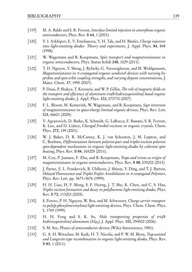
BIBLIOGRAPHY 139
[119] M. A. Baldo and S. R. Forrest, Interface-limited injection in amorphous organicsemiconductors, Phys. Rev. B 64, 1 (2001).
[120] V. I. Arkhipov, E. V. Emelianova, Y. H. Tak, and H. Bässler, Charge injectioninto light-emitting diodes: Theory and experiment, J. Appl. Phys. 84, 848(1998).
[121] W. Wagemans and B. Koopmans, Spin transport and magnetoresistance inorganic semiconductors, Phys. Status Solidi 248, 1029 (2011).
[122] T. D. Nguyen, Y. Sheng, J. Rybicki, G. Veeraraghavan, and M. Wohlgenannt,Magnetoresistance in π-conjugated organic sandwich devices with varying hy-perfine and spin-orbit coupling strengths, and varying dopant concentrations, J.Mater. Chem. 17, 1995 (2007).
[123] P. Desai, P. Shakya, T. Kreouzis, and W. P. Gillin, The role of magnetic fields onthe transport and efficiency of aluminum tris(8-hydroxyquinoline) based organiclight emitting diodes, J. Appl. Phys. 102, 073710 (2007).
[124] F. L. Bloom, M. Kemerink, W. Wagemans, and B. Koopmans, Sign inversionof magnetoresistance in space-charge limited organic devices, Phys. Rev. Lett.103, 66601 (2009).
[125] V. Agranovich, D. Basko, K. Schmidt, G. LaRocca, F. Bassani, S. R. Forrest,K. Leo, and D. Lidzey, Charged Frenkel excitons in organic crystals, Chem.Phys. 272, 159 (2001).
[126] W. J. Baker, D. R. McCamey, K. J. van Schooten, J. M. Lupton, andC. Boehme, Differentiation between polaron-pair and triplet-exciton polaronspin-dependent mechanisms in organic light-emitting diodes by coherent spinbeating, Phys. Rev. B 84, 165205 (2011).
[127] M. Cox, P. Janssen, F. Zhu, and B. Koopmans, Traps and trions as origin ofmagnetoresistance in organic semiconductors, Phys. Rev. B 88, 035202 (2013).
[128] J. Partee, E. L. Frankevich, B. Uhlhorn, J. Shinar, Y. Ding, and T. J. Barton,Delayed Fluorescence and Triplet-Triplet Annihilation in π-conjugated Polymers,Phys. Rev. Lett. pp. 3673–3676 (1999).
[129] H. H. Liao, H. F. Meng, S. F. Horng, J. T. Shy, K. Chen, and C. S. Hsu,Triplet exciton formation and decay in polyfluorene light-emitting diodes, Phys.Rev. B 72, 113203 (2005).
[130] S. Forero, P. H. Nguyen, W. Bru, and M. Schwoerer, Charge carrier transportin poly(p-phenylenevinylene) light-emitting devices, Phys. Chem. Chem. Phys.1, 1769 (1999).
[131] H. H. Fong and S. K. So, Hole transporting properties of tris(8-hydroxyquinoline) aluminum (Alq3), J. Appl. Phys. 100, 094502 (2006).
[132] S. M. Sze, Physics of semiconductor devices (Wiley-Interscience, 1981).
[133] G. A. H. Wetzelaer, M. Kuik, H. T. Nicolai, and P. W. M. Blom, Trap-assistedand Langevin-type recombination in organic light-emitting diodes, Phys. Rev.B 83, 1 (2011).
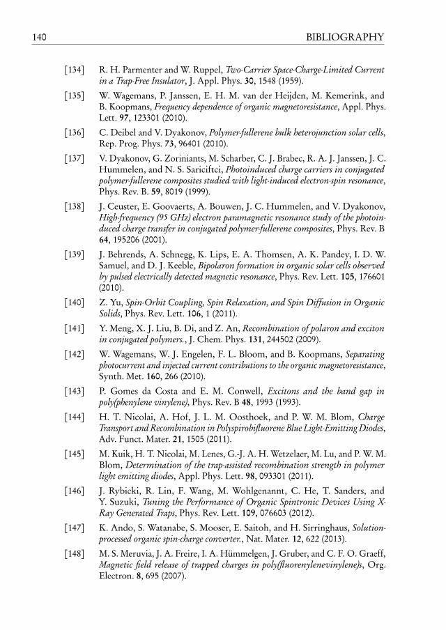
140 BIBLIOGRAPHY
[134] R. H. Parmenter and W. Ruppel, Two-Carrier Space-Charge-Limited Currentin a Trap-Free Insulator, J. Appl. Phys. 30, 1548 (1959).
[135] W. Wagemans, P. Janssen, E. H. M. van der Heijden, M. Kemerink, andB. Koopmans, Frequency dependence of organic magnetoresistance, Appl. Phys.Lett. 97, 123301 (2010).
[136] C. Deibel and V. Dyakonov, Polymer-fullerene bulk heterojunction solar cells,Rep. Prog. Phys. 73, 96401 (2010).
[137] V. Dyakonov, G. Zoriniants, M. Scharber, C. J. Brabec, R. A. J. Janssen, J. C.Hummelen, and N. S. Sariciftci, Photoinduced charge carriers in conjugatedpolymer-fullerene composites studied with light-induced electron-spin resonance,Phys. Rev. B. 59, 8019 (1999).
[138] J. Ceuster, E. Goovaerts, A. Bouwen, J. C. Hummelen, and V. Dyakonov,High-frequency (95 GHz) electron paramagnetic resonance study of the photoin-duced charge transfer in conjugated polymer-fullerene composites, Phys. Rev. B64, 195206 (2001).
[139] J. Behrends, A. Schnegg, K. Lips, E. A. Thomsen, A. K. Pandey, I. D. W.Samuel, and D. J. Keeble, Bipolaron formation in organic solar cells observedby pulsed electrically detected magnetic resonance, Phys. Rev. Lett. 105, 176601(2010).
[140] Z. Yu, Spin-Orbit Coupling, Spin Relaxation, and Spin Diffusion in OrganicSolids, Phys. Rev. Lett. 106, 1 (2011).
[141] Y. Meng, X. J. Liu, B. Di, and Z. An, Recombination of polaron and excitonin conjugated polymers., J. Chem. Phys. 131, 244502 (2009).
[142] W. Wagemans, W. J. Engelen, F. L. Bloom, and B. Koopmans, Separatingphotocurrent and injected current contributions to the organic magnetoresistance,Synth. Met. 160, 266 (2010).
[143] P. Gomes da Costa and E. M. Conwell, Excitons and the band gap inpoly(phenylene vinylene), Phys. Rev. B 48, 1993 (1993).
[144] H. T. Nicolai, A. Hof, J. L. M. Oosthoek, and P. W. M. Blom, ChargeTransport and Recombination in Polyspirobifluorene Blue Light-Emitting Diodes,Adv. Funct. Mater. 21, 1505 (2011).
[145] M. Kuik, H. T. Nicolai, M. Lenes, G.-J. A. H. Wetzelaer, M. Lu, and P. W. M.Blom, Determination of the trap-assisted recombination strength in polymerlight emitting diodes, Appl. Phys. Lett. 98, 093301 (2011).
[146] J. Rybicki, R. Lin, F. Wang, M. Wohlgenannt, C. He, T. Sanders, andY. Suzuki, Tuning the Performance of Organic Spintronic Devices Using X-Ray Generated Traps, Phys. Rev. Lett. 109, 076603 (2012).
[147] K. Ando, S. Watanabe, S. Mooser, E. Saitoh, and H. Sirringhaus, Solution-processed organic spin-charge converter., Nat. Mater. 12, 622 (2013).
[148] M. S. Meruvia, J. A. Freire, I. A. Hümmelgen, J. Gruber, and C. F. O. Graeff,Magnetic field release of trapped charges in poly(fluorenylenevinylene)s, Org.Electron. 8, 695 (2007).
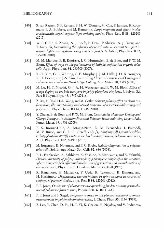
BIBLIOGRAPHY 141
[149] S. van Reenen, S. P. Kersten, S. H. W. Wouters, M. Cox, P. Janssen, B. Koop-mans, P. A. Bobbert, and M. Kemerink, Large magnetic field effects in elec-trochemically doped organic light-emitting diodes, Phys. Rev. B 88, 125203(2013).
[150] W. P. Gillin, S. Zhang, N. J. Rolfe, P. Desai, P. Shakya, A. J. Drew, andT. Kreouzis, Determining the influence of excited states on current transport inorganic light emitting diodes using magnetic field perturbation, Phys. Rev. B 82,195208 (2010).
[151] M. M. Mandoc, F. B. Kooistra, J. C. Hummelen, B. de Boer, and P. W. M.Blom, Effect of traps on the performance of bulk heterojunction organic solarcells, Appl. Phys. Lett. 91, 263505 (2007).
[152] K.-H. Yim, G. L. Whiting, C. E. Murphy, J. J. M. Halls, J. H. Burroughes,R. H. Friend, and J.-S. Kim, Controlling Electrical Properties of ConjugatedPolymers via a Solution-Based p-Type Doping, Adv. Mater. 20, 3319 (2008).
[153] M. Lu, H. T. Nicolai, G.-J. A. H. Wetzelaer, and P. W. M. Blom, Effect ofn-type doping on the hole transport in poly(p-phenylene vinylene), J. Polym. Sci.Part B Polym. Phys. 49, 1745 (2011).
[154] Z. Xu, H. Tsai, H.-L. Wang, and M. Cotlet, Solvent polarity effect on chain con-formation, film morphology, and optical properties of a water-soluble conjugatedpolymer., J. Phys. Chem. B 114, 11746 (2010).
[155] Y. Zhang, B. de Boer, and P. W. M. Blom, Controllable Molecular Doping andCharge Transport in Solution-Processed Polymer Semiconducting Layers, Adv.Funct. Mater. 19, 1901 (2009).
[156] E. S. Bronze-Uhle, A. Batagin-Neto, D. M. Fernandes, I. Fratoddi,M. V. Russo, and C. F. O. Graeff, Poly [1,1’-bis(ethynyl)-4,4’-biphenyl(bis-tributylphosphine)Pt(II)] solutions used as low dose ionizing radiation dosimeter,Appl. Phys. Lett. 102, 241917 (2013).
[157] M. Jørgensen, K. Norrman, and F. C. Krebs, Stability/degradation of polymersolar cells, Sol. Energy Mater. Sol. Cells 92, 686 (2008).
[158] E. L. Frankevich, A. Zakhidov, K. Yoshino, Y. Maruyama, and K. Yakushi,Photoconductivity of poly(2,5-diheptyloxy-p-phenylene vinylene) in the air atmo-sphere: Magnetic-field effect and mechanism of generation and recombination ofcharge carriers., Phys. Rev. B. Condens. Matter 53, 4498 (1996).
[159] K. Kanemoto, H. Matsuoka, Y. Ueda, K. Takemoto, K. Kimura, andH. Hashimoto, Displacement current induced by spin resonance in air-treatedconjugated polymer diodes, Phys. Rev. B 86, 125201 (2012).
[160] P. F. Jones, On the use of phosphorescence quenching for determining permeabil-ities of polymeric films to gases, Polym. Lett. 6, 487 (1968).
[161] P. F. Jones and S. Siegel, Temperature effects on the phosphorescence of aromatichydrocarbons in poly(methylmethacrylate), J. Chem. Phys. 50, 1134 (1969).
[162] B. Lee, Y. Chen, D. Fu, H. T. Yi, K. Czelen, H. Najafov, and V. Podzorov,
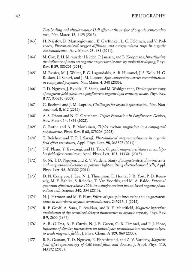
142 BIBLIOGRAPHY
Trap healing and ultralow-noise Hall effect at the surface of organic semiconduc-tors., Nat. Mater. 12, 1125 (2013).
[163] H. Najafov, D. Mastrogiovanni, E. Garfunkel, L. C. Feldman, and V. Pod-zorov, Photon-assisted oxygen diffusion and oxygen-related traps in organicsemiconductors., Adv. Mater. 23, 981 (2011).
[164] M. Cox, E. H. M. van der Heijden, P. Janssen, and B. Koopmans, Investigatingthe influence of traps on organic magnetoresistance by molecular doping, Phys.Rev. B 89, 085201 (2014).
[165] M. Reufer, M. J. Walter, P. G. Lagoudakis, A. B. Hummel, J. S. Kolb, H. G.Roskos, U. Scherf, and J. M. Lupton, Spin-conserving carrier recombinationin conjugated polymers, Nat. Mater. 4, 340 (2005).
[166] T. D. Nguyen, J. Rybicki, Y. Sheng, and M. Wohlgenannt, Device spectroscopyof magnetic field effects in a polyfluorene organic light-emitting diode, Phys. Rev.B 77, 035210 (2008).
[167] C. Boehme and J. M. Lupton, Challenges for organic spintronics., Nat. Nan-otechnol. 8, 612 (2013).
[168] A. S. Dhoot and N. C. Greenham, Triplet Formation In Polyfluorene Devices,Adv. Mater. 14, 1834 (2002).
[169] C. Rothe and A. P. Monkman, Triplet exciton migration in a conjugatedpolyfluorene, Phys. Rev. B 68, 075208 (2003).
[170] T. Reichert and T. P. I. Saragi, Photoinduced magnetoresistance in organicfield-effect transistors, Appl. Phys. Lett. 98, 063307 (2011).
[171] S.-T. Pham, Y. Kawasugi, and H. Tada, Organic magnetoresistance in ambipo-lar field-effect transistors, Appl. Phys. Lett. 103, 143301 (2013).
[172] G. Ni, T. D. Nguyen, and Z. V. Vardeny, Study of magneto-electroluminescenceand magneto-conductance in polymer light-emitting electrochemical cells, Appl.Phys. Lett. 98, 263302 (2011).
[173] D. N. Congreve, J. Lee, N. J. Thompson, E. Hontz, S. R. Yost, P. D. Reuss-wig, M. E. Bahlke, S. Reineke, T. Van Voorhis, and M. A. Baldo, Externalquantum efficiency above 100% in a singlet-exciton-fission-based organic photo-voltaic cell., Science 340, 334 (2013).
[174] N. J. Harmon and M. E. Flatt, Effects of spin-spin interactions on magnetoresis-tance in disordered organic semiconductors, 245213, 1 (2012).
[175] R. P. Groff, A. Suna, P. Avakian, and R. E. Merrifield, Magnetic hyperfinemodulation of dye-sensitized delayed fluorescence in organic crystals, Phys. Rev.B 9, 2655 (1974).
[176] A. R. O’Dea, A. F. Curtis, N. J. B. Green, C. R. Timmel, and P. J. Hore,Influence of dipolar interactions on radical pair recombination reactions subjectto weak magnetic fields., J. Phys. Chem. A 109, 869 (2005).
[177] B. R. Gautam, T. D. Nguyen, E. Ehrenfreund, and Z. V. Vardeny, Magneticfield effect spectroscopy of C60-based films and devices, J. Appl. Phys. 113,143102 (2013).
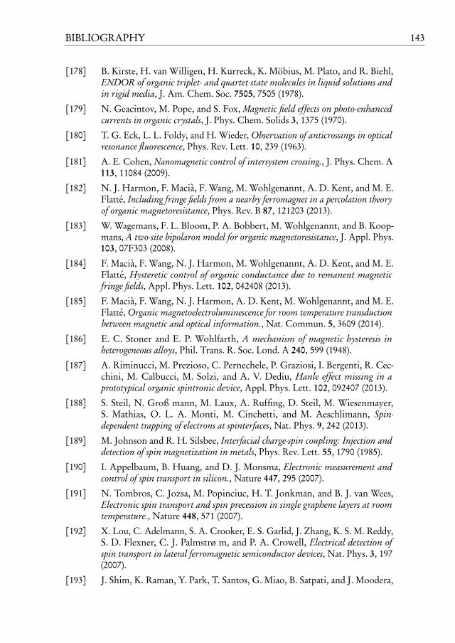
BIBLIOGRAPHY 143
[178] B. Kirste, H. van Willigen, H. Kurreck, K. Möbius, M. Plato, and R. Biehl,ENDOR of organic triplet- and quartet-state molecules in liquid solutions andin rigid media, J. Am. Chem. Soc. 7505, 7505 (1978).
[179] N. Geacintov, M. Pope, and S. Fox, Magnetic field effects on photo-enhancedcurrents in organic crystals, J. Phys. Chem. Solids 3, 1375 (1970).
[180] T. G. Eck, L. L. Foldy, and H. Wieder, Observation of anticrossings in opticalresonance fluorescence, Phys. Rev. Lett. 10, 239 (1963).
[181] A. E. Cohen, Nanomagnetic control of intersystem crossing., J. Phys. Chem. A113, 11084 (2009).
[182] N. J. Harmon, F. Macià, F. Wang, M. Wohlgenannt, A. D. Kent, and M. E.Flatté, Including fringe fields from a nearby ferromagnet in a percolation theoryof organic magnetoresistance, Phys. Rev. B 87, 121203 (2013).
[183] W. Wagemans, F. L. Bloom, P. A. Bobbert, M. Wohlgenannt, and B. Koop-mans, A two-site bipolaron model for organic magnetoresistance, J. Appl. Phys.103, 07F303 (2008).
[184] F. Macià, F. Wang, N. J. Harmon, M. Wohlgenannt, A. D. Kent, and M. E.Flatté, Hysteretic control of organic conductance due to remanent magneticfringe fields, Appl. Phys. Lett. 102, 042408 (2013).
[185] F. Macià, F. Wang, N. J. Harmon, A. D. Kent, M. Wohlgenannt, and M. E.Flatté, Organic magnetoelectroluminescence for room temperature transductionbetween magnetic and optical information., Nat. Commun. 5, 3609 (2014).
[186] E. C. Stoner and E. P. Wohlfarth, A mechanism of magnetic hysteresis inheterogeneous alloys, Phil. Trans. R. Soc. Lond. A 240, 599 (1948).
[187] A. Riminucci, M. Prezioso, C. Pernechele, P. Graziosi, I. Bergenti, R. Cec-chini, M. Calbucci, M. Solzi, and A. V. Dediu, Hanle effect missing in aprototypical organic spintronic device, Appl. Phys. Lett. 102, 092407 (2013).
[188] S. Steil, N. Groß mann, M. Laux, A. Ruffing, D. Steil, M. Wiesenmayer,S. Mathias, O. L. A. Monti, M. Cinchetti, and M. Aeschlimann, Spin-dependent trapping of electrons at spinterfaces, Nat. Phys. 9, 242 (2013).
[189] M. Johnson and R. H. Silsbee, Interfacial charge-spin coupling: Injection anddetection of spin magnetization in metals, Phys. Rev. Lett. 55, 1790 (1985).
[190] I. Appelbaum, B. Huang, and D. J. Monsma, Electronic measurement andcontrol of spin transport in silicon., Nature 447, 295 (2007).
[191] N. Tombros, C. Jozsa, M. Popinciuc, H. T. Jonkman, and B. J. van Wees,Electronic spin transport and spin precession in single graphene layers at roomtemperature., Nature 448, 571 (2007).
[192] X. Lou, C. Adelmann, S. A. Crooker, E. S. Garlid, J. Zhang, K. S. M. Reddy,S. D. Flexner, C. J. Palmstrø m, and P. A. Crowell, Electrical detection ofspin transport in lateral ferromagnetic semiconductor devices, Nat. Phys. 3, 197(2007).
[193] J. Shim, K. Raman, Y. Park, T. Santos, G. Miao, B. Satpati, and J. Moodera,
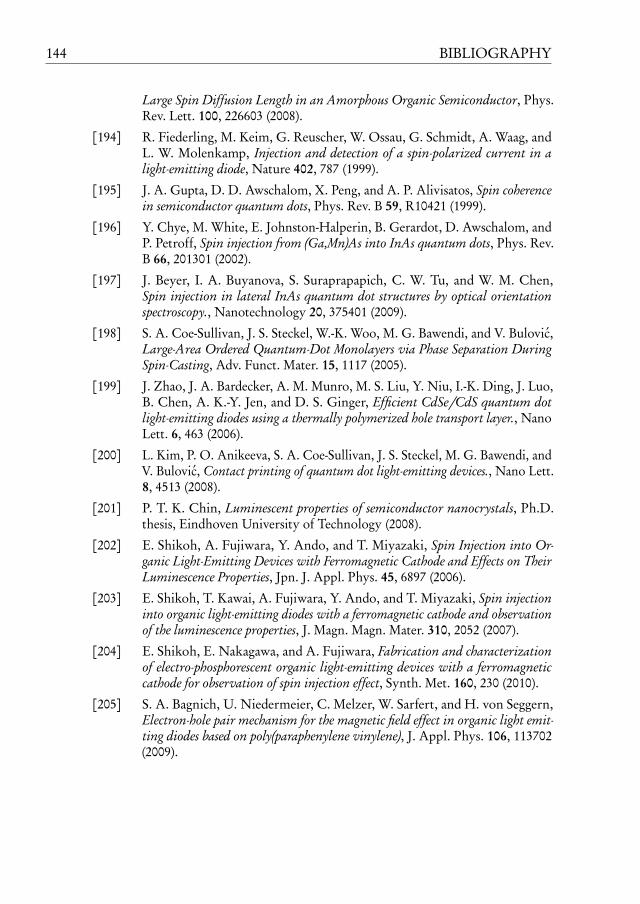
144 BIBLIOGRAPHY
Large Spin Diffusion Length in an Amorphous Organic Semiconductor, Phys.Rev. Lett. 100, 226603 (2008).
[194] R. Fiederling, M. Keim, G. Reuscher, W. Ossau, G. Schmidt, A. Waag, andL. W. Molenkamp, Injection and detection of a spin-polarized current in alight-emitting diode, Nature 402, 787 (1999).
[195] J. A. Gupta, D. D. Awschalom, X. Peng, and A. P. Alivisatos, Spin coherencein semiconductor quantum dots, Phys. Rev. B 59, R10421 (1999).
[196] Y. Chye, M. White, E. Johnston-Halperin, B. Gerardot, D. Awschalom, andP. Petroff, Spin injection from (Ga,Mn)As into InAs quantum dots, Phys. Rev.B 66, 201301 (2002).
[197] J. Beyer, I. A. Buyanova, S. Suraprapapich, C. W. Tu, and W. M. Chen,Spin injection in lateral InAs quantum dot structures by optical orientationspectroscopy., Nanotechnology 20, 375401 (2009).
[198] S. A. Coe-Sullivan, J. S. Steckel, W.-K. Woo, M. G. Bawendi, and V. Bulovic,Large-Area Ordered Quantum-Dot Monolayers via Phase Separation DuringSpin-Casting, Adv. Funct. Mater. 15, 1117 (2005).
[199] J. Zhao, J. A. Bardecker, A. M. Munro, M. S. Liu, Y. Niu, I.-K. Ding, J. Luo,B. Chen, A. K.-Y. Jen, and D. S. Ginger, Efficient CdSe/CdS quantum dotlight-emitting diodes using a thermally polymerized hole transport layer., NanoLett. 6, 463 (2006).
[200] L. Kim, P. O. Anikeeva, S. A. Coe-Sullivan, J. S. Steckel, M. G. Bawendi, andV. Bulovic, Contact printing of quantum dot light-emitting devices., Nano Lett.8, 4513 (2008).
[201] P. T. K. Chin, Luminescent properties of semiconductor nanocrystals, Ph.D.thesis, Eindhoven University of Technology (2008).
[202] E. Shikoh, A. Fujiwara, Y. Ando, and T. Miyazaki, Spin Injection into Or-ganic Light-Emitting Devices with Ferromagnetic Cathode and Effects on TheirLuminescence Properties, Jpn. J. Appl. Phys. 45, 6897 (2006).
[203] E. Shikoh, T. Kawai, A. Fujiwara, Y. Ando, and T. Miyazaki, Spin injectioninto organic light-emitting diodes with a ferromagnetic cathode and observationof the luminescence properties, J. Magn. Magn. Mater. 310, 2052 (2007).
[204] E. Shikoh, E. Nakagawa, and A. Fujiwara, Fabrication and characterizationof electro-phosphorescent organic light-emitting devices with a ferromagneticcathode for observation of spin injection effect, Synth. Met. 160, 230 (2010).
[205] S. A. Bagnich, U. Niedermeier, C. Melzer, W. Sarfert, and H. von Seggern,Electron-hole pair mechanism for the magnetic field effect in organic light emit-ting diodes based on poly(paraphenylene vinylene), J. Appl. Phys. 106, 113702(2009).


