managed 10/100base-tx / fx media converter · managed 10/100base-tx / fx media converter features a...
TRANSCRIPT

IP113F LFPreliminary Data Sheet
Confidential. 1/58 February 21, 2005Copyright © 2004, IC Plus Corp. IP113F LF-DS-R08
Managed 10/100Base-TX / FX Media Converter
Features
A 10/100BASE-TX/ 100BASE-FX converter with a SMI port for management
Built in a 10/100BASE-TX transceiver Built in a PHY for 100BASE-FX Built in a 2-port switch
– Pass all packets without address and CRC check (optional)
– Supports modified cut-through frame forwarding for low latency
– Supports pure converter mode data forwarding for extreme low latency
– Supports flow control for full and half duplex operation
– Bandwidth control – Max packet length 1600 bytes – Optional forward fragments
Built in 128Kb RAM for data buffer Supports 3.3v I/O tolerance SMI (MDC, MDIO)
and MII registers for management – Configure local and remote IP113F LF
through local SMI – Monitor local and remote IP113F LF
through local SMI – Configure/ monitor TP port support
(auto-negotiation or force 10M/100M, full/half)
– Configure/ monitor flow control, bandwidth – Supports loop back test (In-band or
out-band, auto or program) – The maintenance frame is compliant to
TS-1000 standard (the Telecommunication Technology Committee, TTC)
Supports Statistic Counters Supports auto MDI-MDIX function Supports link fault pass through function Supports far end fault function LED display for link/activity, full/half, 10/100 Built in a watchdog timer to monitor internal
switch error Supports EEPROM Configuration 0.25u CMOS technology Single 2.5V power supply 48-pin LQFP package Support Lead Free package (Please refer to the
Order Information)
General Description
IP113F LF can be a 10/100BASE-TX to 100BASE-FX converter or a 100BASE-FX to 100BASE-FX repeater with an SMI port for management. It consists of a 2-port switch controller, a fast Ethernet transceiver and a PHY for 100BASE-FX. The transceivers in IP113F LF are designed in DSP approach with advance 0.25um technology; this results in high noise immunity and robust performance. IP113F LF not only supports store and forward mode, it also supports modified cut through mode and pure converter mode for low latency data forwarding. IP113F LF can transmit packet(s) up to 1600 bytes to meet requirement of extra long packets. IP113F LF supports remote management function. IP113F LF supports remote access functions and it also supports remote monitor and loop back test function defined in TS-1000 spec (*). Local IP113F LF can access the MII registers of remote IP113F LF by programming local IP113F LF’s MII registers via SMI connection. IP113F LF implements the management function using the maintenance frame defined in TS-1000 spec. IP113F LF supports IEEE802.3x, collision base backpressure, and various LED functions, etc. These functions can be configured to fit the different requirements by feeding operation parameters via EEPROM interface or pull up/down resistors on specified pins. * The Telecommunication Technology Committee owns the copyright of TS-1000.

IP113F LFPreliminary Data Sheet
Confidential. 2/58 February 21, 2005Copyright © 2004, IC Plus Corp. IP113F LF-DS-R08
Contents
Features....................................................................................................................................................... 1 General Description..................................................................................................................................... 1 Contents ...................................................................................................................................................... 2 Revision History........................................................................................................................................... 4 Block Diagram ............................................................................................................................................. 5 Application Diagram .................................................................................................................................... 5 Applications ................................................................................................................................................. 6
Managed converter (up to 31 pieces of IP113F LF in a chassis) ............................................. 6 Un-managed converter.............................................................................................................. 6 Fiber Repeater........................................................................................................................... 6
PIN Diagram ................................................................................................................................................ 7 1. PIN Description ................................................................................................................................... 8
PIN Description (continued) ...................................................................................................... 9 PIN Description (continued) .................................................................................................... 10 PIN Description (continued) .....................................................................................................11 PIN Description (continued) .................................................................................................... 12 PIN Description (continued) .................................................................................................... 13
2. Functional Description ...................................................................................................................... 14 2.1 Data forwarding............................................................................................................... 14
2.1.1 Modified cut-through mode ........................................................................... 14 2.1.2 Pure converter mode..................................................................................... 14 2.1.3 Fragment forwarding ..................................................................................... 14
2.2 TP port force mode ......................................................................................................... 15 2.3 Remote management ..................................................................................................... 16
2.3.1 Maintenance frame format at MII .................................................................. 16 2.3.2 Bit definition of maintenance frame............................................................... 16 2.3.3 Bit definition of maintenance frame (continued)............................................ 17 2.3.4 Remote monitor............................................................................................. 18 2.3.5 Remote control read...................................................................................... 18 2.3.6 Remote control write ..................................................................................... 18
2.4 Loop back test ................................................................................................................ 19 2.4.1 Out-band loop back test ................................................................................ 19 2.4.2 In-band loop back test ................................................................................... 21 2.4.3 Programming procedure for In-band loop back test...................................... 22 2.4.4 Auto in-band loop back test........................................................................... 22
2.5 Remote monitor without SMI programming.................................................................... 23 2.5.1 Auto sends (Status change notice) ............................................................... 23
2.6 Link fault pass through.................................................................................................... 24 2.6.1 Normal case .................................................................................................. 24 2.6.2 Remote TP port disconnected....................................................................... 24 2.6.3 FX port disconnected....................................................................................... 25 2.6.4 LED diagnostic functions for fault indication ................................................. 25
2.7 EEPROM – store the initial value ................................................................................... 26 2.8 Auto MDI_MDIX.............................................................................................................. 27 2.9 Serial management interface.......................................................................................... 28
3. MII registers ...................................................................................................................................... 29 3.1 The basic MII registers ................................................................................................... 30
The basic MII registers 0........................................................................................... 30 The basic MII registers 1........................................................................................... 32 The basic MII registers 1(continued) ........................................................................ 33 The basic MII registers 2 , 3...................................................................................... 34 The basic MII registers 4........................................................................................... 35

IP113F LFPreliminary Data Sheet
Confidential. 3/58 February 21, 2005Copyright © 2004, IC Plus Corp. IP113F LF-DS-R08
The basic MII registers 5......................................................................................... 36 The basic MII registers 6......................................................................................... 37
3.2 Extended MII registers and EEPROM registers ........................................................... 38 Extended MII registers and EEPROM registers 16 ................................................ 39 Extended MII registers and EEPROM registers 17 ................................................ 40 Extended MII registers and EEPROM registers 17(continued) .............................. 41 Extended MII registers and EEPROM registers 18 ................................................ 42 Extended MII registers and EEPROM registers 19 ................................................ 43 Extended MII registers and EEPROM registers 20 ................................................ 44 Extended MII registers and EEPROM registers 20(continued) .............................. 45 Extended MII registers and EEPROM registers 21 ................................................ 46 Extended MII registers and EEPROM registers 22 ................................................ 47 Extended MII registers and EEPROM registers 22(continued) .............................. 48 Extended MII registers and EEPROM registers 23 ................................................ 49 Extended MII registers and EEPROM registers 23(continued) .............................. 50 Extended MII registers and EEPROM registers 24 ................................................ 51 Extended MII registers and EEPROM registers 25 ................................................ 52 Extended MII registers and EEPROM registers 26 ................................................ 53 Extended MII registers and EEPROM registers 27,28,29,30 ................................. 54 Extended MII registers and EEPROM registers 31 ................................................ 55
4. Electrical Characteristics .................................................................................................................. 57 4.1 Absolute Maximum Rating.............................................................................................. 57 4.2. DC Characteristic........................................................................................................... 57
5. Order Information.............................................................................................................................. 57 6. Package Detail.................................................................................................................................. 58
IP113F LFPreliminary Data Sheet
Confidential. 4/58 February 21, 2005Copyright © 2004, IC Plus Corp. IP113F LF-DS-R08
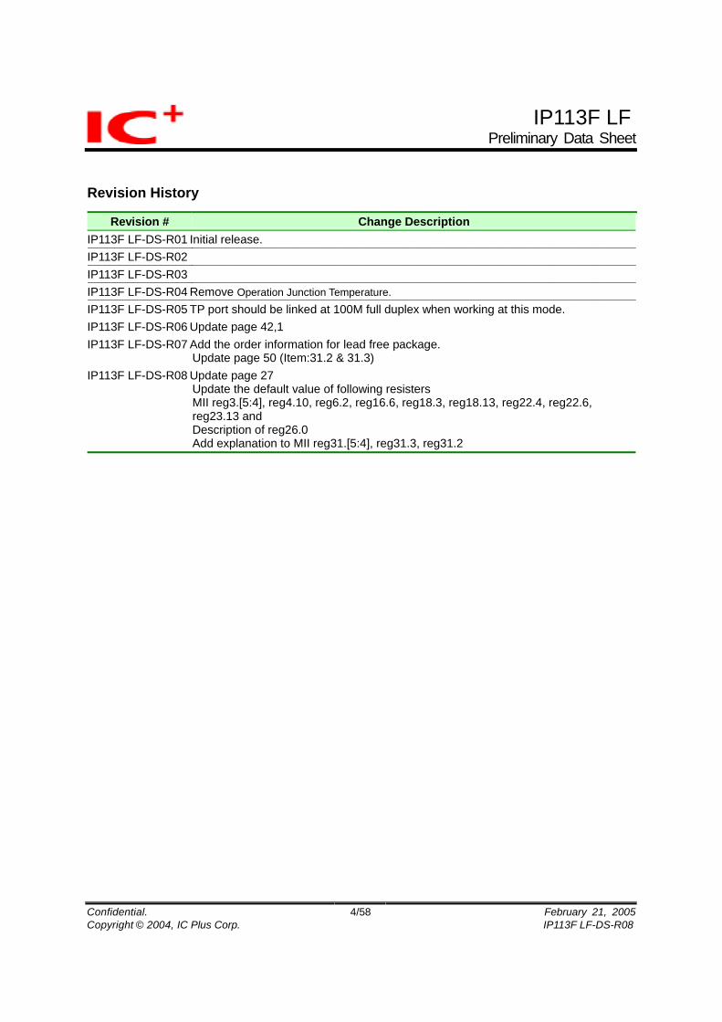
Revision History
Revision # Change Description IP113F LF-DS-R01 Initial release. IP113F LF-DS-R02 IP113F LF-DS-R03 IP113F LF-DS-R04 Remove Operation Junction Temperature. IP113F LF-DS-R05 TP port should be linked at 100M full duplex when working at this mode. IP113F LF-DS-R06 Update page 42,1 IP113F LF-DS-R07 Add the order information for lead free package.
Update page 50 (Item:31.2 & 31.3) IP113F LF-DS-R08 Update page 27
Update the default value of following resisters MII reg3.[5:4], reg4.10, reg6.2, reg16.6, reg18.3, reg18.13, reg22.4, reg22.6, reg23.13 and Description of reg26.0 Add explanation to MII reg31.[5:4], reg31.3, reg31.2

IP113F LFPreliminary Data Sheet
Confidential. 5/58 February 21, 2005Copyright © 2004, IC Plus Corp. IP113F LF-DS-R08
Block Diagram
10/100M TXPHY Two port switch
SSRAMMII registers
EEPROMI/F
RemoteControl
100M FX
PLL/ ClockGenerator
LEDI/F
Forward ModeControl
MDCMDIO
RXIPRXIM
SCLSDA
MII MII
LED
TXOPTXOM
FXSDFXRDPFXRDMFXTDPFXTDM
Application Diagram
IP113F LF
Fiber Module
TX
FX

IP113F LFPreliminary Data Sheet
Confidential. 6/58 February 21, 2005Copyright © 2004, IC Plus Corp. IP113F LF-DS-R08
Applications
Managed converter (up to 31 pieces of IP113F LF in a chassis)
IP113F LFMDC, MDIO uC
(for management)
FAST_FWD
X 31X 1
VCC
Un-managed converter
IP113F LF
PHY1
PHY2
SWITCH10BASE_T/100BASE-TX
100BASE-FX RAM
Fiber Repeater
TWO_FIBER
IP113F LF
VCC
PHY1
PHY2
SWITCH100BASE-FX
100BASE-FX RAM
IP113F LFPreliminary Data Sheet
Confidential. 7/58 February 21, 2005Copyright © 2004, IC Plus Corp. IP113F LF-DS-R08
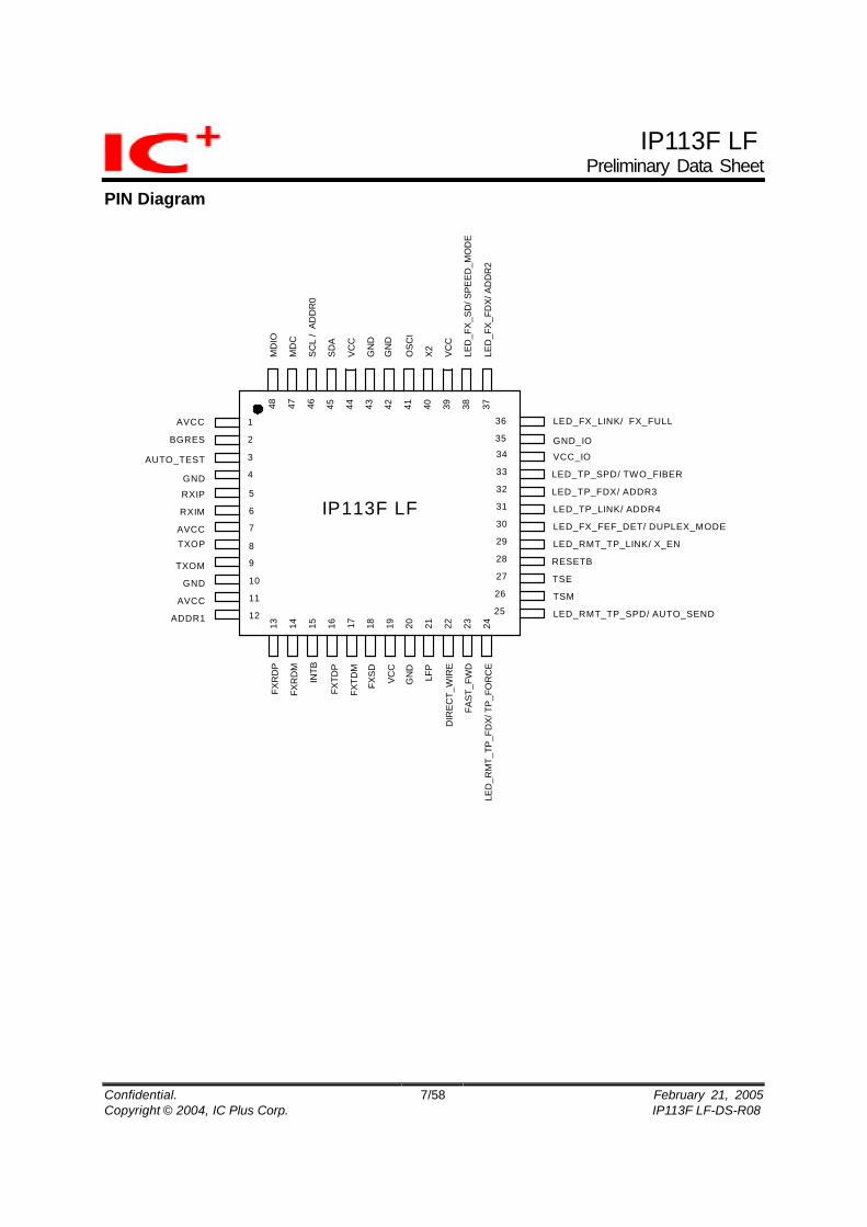
PIN Diagram
AUTO_TEST
1
2
3
4
12
5
6
7
8
9
10
11
36
26
25
35
32
31
30
28
29
27
34
332422 23212019181716151413
3839404142434445464748
FAS
T_FW
DGND
RXIP
LFP
GN
D
ADDR1
AVCC
GND
TXOM
AVCC
RXIM
FXR
DM
DIR
ECT_
WIR
E
VCC
FXS
D
FXTD
P
FXTD
M
LED_RMT_TP_SPD/ AUTO_SEND
TSM
RESETB
TSE
LED_RMT_TP_LINK/ X_EN
LED_FX_FEF_DET/ DUPLEX_MODE
LED_TP_FDX/ ADDR3
LED_TP_LINK/ ADDR4
LED_FX_LINK/ FX_FULL
LED
_FX
_SD
/ SPE
ED_M
OD
E
VC
C
X2
GN
D
VC
C
OSC
I
SD
A
SC
L /
ADD
R0
MD
C
MD
IO
BGRES
VCC_IO
GND_IO
GN
D
37LE
D_F
X_F
DX/
AD
DR
2
IP113F LF
TXOP
FXR
DP
AVCC
INTB
LED
_RM
T_TP
_FD
X/ T
P_FO
RC
ELED_TP_SPD/ TWO_FIBER

IP113F LFPreliminary Data Sheet
Confidential. 8/58 February 21, 2005Copyright © 2004, IC Plus Corp. IP113F LF-DS-R08
1. PIN Description
Type Description I Input pin O Output pin
IPH Input pin with pull-high resistor IPL Input pin with pull-low resistor
Pin no. Label Type Description Transceiver 5, 6 RXIP, RXIM I TP receive 8, 9 TXOP, TXOM O TP transmit 2 BGRES O Band gap resistor
It is connected to GND through a 6.19k (1%) resistor in application circuit.
18 FXSD I 100Base-FX signal detect Fiber signal detect. It is an input signal from fiber MAU. Fiber signal detect is active if the voltage on FXSD is higher than the threshold voltage, which is 1.35v ±5% when VCC is equal to 2.5v.
13, 14 FXRDP, FXRDM I Fiber receiver data pair 16, 17 FXTDP, FXTDM O Fiber transmit data pair

IP113F LFPreliminary Data Sheet
Confidential. 9/58 February 21, 2005Copyright © 2004, IC Plus Corp. IP113F LF-DS-R08
PIN Description (continued)
Pin no. Label Type Description LED pins 31 LED_TP_LINK O TP port link LED
On: link ok, Off: link fail, Flash: link ok & activity (Flash: on for 20ms and off for 80ms)
33 LED_TP_SPD O TP port speed LED On: 100M, Off: 10M
32 LED_TP_FDX O TP port full duplex LED On: full, Off: half, Flash: half & collision happens (Flash: on for 20ms and off for 80ms)
36 LED_FX_LINK O Fiber port link LED On: link ok, Off: link fail, Flash: link ok & activity (Flash: on for 20ms and off for 80ms)
37 LED_FX_FDX O Fiber port full duplex LED On: full, Off: half, Flash: half & collision happens (Flash: on for 20ms and off for 80ms)
38 LED_FX_SD O Fiber port signal detect On: FXSD is active, Off: FXSD is inactive
30 LED_FX_FEF_DET O Far end fault pattern received Far End Fault Pattern received: LED On: 80ms, LED Off: 20ms Far End Fault Pattern not Receive: LED is always off LED for link status of TP port of remote IP113F LF Pin 3 AUTO_TEST = 0 Pin 3 AUTO_TEST = 1
29 LED_RMT_TP_LINK O
On: link ok, Off: link fail
Flash (On: 80ms, Off: 20ms)
LED for speed of TP port of remote IP113F LF Pin 3 AUTO_TEST = 0 Pin 3 AUTO_TEST = 1
25 LED_RMP_TP_SPD O
On: 100M, Off: 10M
On: loop back test complete, Off: under loop back test
LED for full duplex of TP port of remote IP113F LF Pin 3 AUTO_TEST = 0 Pin 3 AUTO_TEST = 1
24 LED_RMT_TP_FDX O
On: full duplex, Off: half duplex
On: loop back test result is ok, Off: loop back test result fails
Note: The output of LED pin is logic low when the LED is on.

IP113F LFPreliminary Data Sheet
Confidential. 10/58 February 21, 2005Copyright © 2004, IC Plus Corp. IP113F LF-DS-R08
PIN Description (continued)
Pin no. Label Type Description LED pins used as initial setting mode during reset 29 X_EN IPH Flow control enable on TP port and fiber port
1: enable (default), 0: disable
24 TP_FORCE IPL Local TP port auto negotiation enable 1: TP port supports auto-negotiation with limited capability
defined by pin 38 SPEED_MODE and pin 30 DUPLEX_MODE.
0: TP port supports auto-negotiation with 10M/100M, full/ half capability (default)
The setting may be updated by programming EEPROM register 3.5 or MII register 20.13.
38 SPEED_MODE IPH Local TP port speed selection 1: TP port has the 100Mb speed ability 0: TP port has the 10Mb speed ability only
It is valid only if pin 24 TP_FORCE is enabled. 30 DUPLEX_MODE IPH Local TP port duplex selection
1: TP port has the full duplex ability 0: TP port has the half duplex ability only
It is valid only if pin 24 TP_FORCE is enabled. 25 AUTO_SEND IPL Auto send the status to the remote IP113F LF
1: enable 0: disable (default)
36 FX_FULL IPH Set the duplex of fiber port 1: full duplex (default) 0: half duplex
3 AUTO_TEST IPL Auto loop back test 1: enable When IP113F LF detects a low-to-high transition on this pin, it will perform loop back test for once. It supports an easy way to instruct IP113F LF performing fiber loop back test without programming MII registers. 0: disable (default)

IP113F LFPreliminary Data Sheet
Confidential. 11/58 February 21, 2005Copyright © 2004, IC Plus Corp. IP113F LF-DS-R08
PIN Description (continued)
Pin no. Label Type Description LED pins used as initial setting mode during reset 33 TWO_FIBER
IPL Two fiber ports
1: IP113F LF supports two-fiber ports mode. Both port 1 and port 2 are fiber ports. RXIP and RXIM are used as FXRDP and FXRDM for the second fiber port. TXOP and TXOM are used as FXTDP and FXTDM for the second fiber port.
A special requirement for the fiber MAU of port1 in this application is that the output of FXRDP and FXRDM should have no incoming signals when fiber is unplugged.
For some fiber MAUs, there are amplified noisy signals on FXRDP and FXRDM when fiber is unplugged. These amplified noisy signals, which include coupled idle patterns from FXTDP and FXTDM will cause the LEDs of port1 malfunction
Generally, a 3.3-V small form factor type fiber MAUs (e.g. Agilent HFBR-5903) can meet this special requirement, but 5-V duplex-SC and -ST type fiber MAUs cannot. Port2 is not limited by this special requirement.
0: IP113F LF supports one fiber port and one TP port. Port 1 is a TP port and port 2 is a fiber port.

IP113F LFPreliminary Data Sheet
Confidential. 12/58 February 21, 2005Copyright © 2004, IC Plus Corp. IP113F LF-DS-R08
PIN Description (continued)
Pin no. Label Type Description MC operation mode 21 LFP IPL Link fault pass through (LFP)
1: enable Link status of one port is forwarded to the other port. 0: disable (default)
22 23
DIRECT_WIRE FAST_FWD
IPL
DIRECT_WIRE
FAST_FWD Function
0 0 Store and forward switch mode (default)
0 1 Modified cut-through switch mode1 0 Converter mode 1 1 Converter mode with
auto-change-forward function Store and forward switch mode: IP113F LF begins to forward a frame at the end of receiving a frame completely. Modified cut-through switch mode: IP113F LF begins to forward a frame after the first 64 bytes data received. TP port should be forced at 100M at this mode. Converter mode: Incoming frames are not buffered in IP113F LF to achieve the min latency. Both TP port and fiber port of IP113F LF should work at 100M full duplex in this mode. If TP port is linked at half duplex, the total length of UTP cable and fiber should be less than 60 meters to meet the requirement of CSMACD in IEEE802.3. Converter mode with auto-change-forward function: IP113F LF will change forward mode itself if it detects the speed is different in TP port and FX port. In converter mode, IP113F LF forwards IEEE802.3x pause frame directly. In the other modes, IP113F LF doesn’t forward IEEE802.3x pause frame directly, it sends out pause frame when its internal buffer is full.

IP113F LFPreliminary Data Sheet
Confidential. 13/58 February 21, 2005Copyright © 2004, IC Plus Corp. IP113F LF-DS-R08
PIN Description (continued)
Pin no. Label Type Description SMI interface 47, 48 MDC, MDIO I, IO SMI interface
The external MAC device uses the interface to program IP113F LF. MDIO is an open drain.
31, 32, 37, 12, 46
ADDR[4:0] IPL PHY address The external MAC device uses the address to identify each IP113F LF in a chassis. IP113F LF also uses ADDR[2:0] as EEPROM address A[2:0] to read EEPROM.
Pin no. Label Type Description EEPROM interface 45, 46 SDA, SCL IPH, O EEPROM interface
Pin no. Label Type Description Misc. 28 RESETB I Reset
It is low active. 41, 40 OSCI, X2 I, O Crystal pins
OSCI and X2 are connected to a 25Mhz crystal. If a 25MHz oscillator is used, OSCI is connected to the oscillator’s output and X2 should be left open.
26, 27 TSM, TSE IPL Scan pins These two pins should be left open or connected to ground for normal operation.
15 INTB O Interrupt 0: an interrupt happens. Its output is low. 1: no interrupt. Its output is high impedance and it needs an external pull up resistor.

IP113F LFPreliminary Data Sheet
Confidential. 14/58 February 21, 2005Copyright © 2004, IC Plus Corp. IP113F LF-DS-R08
2. Functional Description
2.1 Data forwarding IP113F LF supports three types of data forwarding mode, store & forward mode, modified cut-through mode and pure converter mode. It can forward a frame despite of its address and CRC error. IP113F LF begins to forward the received data when it receives the frame completely. The latency depends on the packet length. 2.1.1 Modified cut-through mode IP113F LF begins to forward the received data when it receives the first 64 bytes of the frame. The latency is about 512 bits time width. The maximum packet length is up to1600 bytes in this mode. Please refer to pin description of FAST_FWD for configuration information. 2.1.2 Pure converter mode IP113F LF operates with the minimum latency in this mode. The transmission flow does not wait until entire frame is ready, but instead it forwards the received data immediately after the data being received. Both transceivers are interconnected via internal MIIs and the internal switch engine and data buffer are not used. Both TP port and fiber port of IP113F LF should work at 100M full duplex in this mode. If TP port is linked at half duplex, the total length of UTP cable and fiber should be less than 60 meters to meet the requirement of CSMACD in IEEE802.3. The packet length is not limited at this mode. Please refer to pin description of DIRECT_WIRE for configuration information. In converter mode, it is strongly recommended that both TP port and fiber port of IP113F LF should work at 100M full duplex. If TP port is linked at half duplex, the UTP cable length should be less than 30 meters to meet the requirement of CSMACD in IEEE802.3. 2.1.3 Fragment forwarding IP113F LF forwards CRC error packets but it will filter fragments when it works in modified cut-through mode. IP113F LF forwards fragments if user turns on bit 3 of MII register 20.

IP113F LFPreliminary Data Sheet
Confidential. 15/58 February 21, 2005Copyright © 2004, IC Plus Corp. IP113F LF-DS-R08
2.2 TP port force mode The TP port of IP113F LF can work at auto mode or force mode. The following table shows all of the combination of its TP port.
Link partner’s capability AN on AN off
IP113F LF’s link result TP_FORCE, SPEED_MODE, DUPLEX_MODE IP113F LF’s capability
100F 100H 10F 10H 100F 100H 10F 10H
011 100/10M, Full/Half, AN on 100F 100H 10F 10H 100H 100H 10H 10H010 100/10M, Half, AN on X 100H X 10H 100H 100H 10H 10H001 10M, Full/Half, AN on X X 10F 10H 100H 100H 10H 10H000 10M, Half, AN on X X X 10H 100H 100H 10H 10H111 100M, Full, AN on 100F X X X 100F 100F X X 110 100M, Half, AN on X 100H X X 100H 100H X X 101 10M, Full, AN on X X 10F X X X 10F 10F100 10M, Half, AN on X X X 10H X X 10H 10H Note: AN on: with auto-negotiation capability AN off: without auto-negotiation capability 100F: 100M full duplex 100H: 100M half duplex 10F: 10M full duplex 10H: 10M half duplex

IP113F LFPreliminary Data Sheet
Confidential. 16/58 February 21, 2005Copyright © 2004, IC Plus Corp. IP113F LF-DS-R08
2.3 Remote management IP113F LF supports remote monitor and configuration function. IP113F LF implement the function by exchanging maintenance frames on fiber ports between two IP113F LF’s. The maintenance frames are not forwarded to TP ports. The frame format follows the TS-1000 standard. 2.3.1 Maintenance frame format at MII TXD0 F0 F4 C0 C4 C8 C12 S0 S4 S8 S12 M0 M4 M8 M12M16M20M24M28M32 M36 M40 M44 E0 E4TXD1 F1 F5 C1 C5 C9 C13 S1 S5 S9 S13 M1 M5 M9 M13M17M21M25M29M33 M37 M41 M45 E1 E5TXD2 F2 F6 C2 C6 C10 C14 S2 S6 S10 S14 M2 M6 M10M14M18M22M26M30M34 M38 M42 M46 E2 E6TXD3 F3 F7 C3 C7 C11 C15 S3 S7 S11 S15 M3 M7 M11M15M19M23M27M31M35 M39 M43 M47 E3 E7
TXEN
2.3.2 Bit definition of maintenance frame
Bit Item Description NoteF7 – F0 Preamble 01010101 Fixed C0 Discriminator for the
maintenance signal 0 Fixed
C1 Direction 0: terminal MC central MC 1: central MC terminal MC (MC: media converter)
C3 – C2 Command 00: Reserved 10: Indication 01: Request 11: Acknowledge
C7 – C4 Version 0000 Fixed C15 C8 Function 0 0 0 0 0 0 01 Loop test start 0 0 0 0 0 0 00 Loop test finished 0 0 0 0 0 0 10 Status indication
C15 – C8 Control signal
Address [4:0] R/W 11 R/W link partner’s registers
S0 Condition of power 0: normal, 1: power off S1 Situation of receiving optical
power 0: normal, 1: abnormal
S2 Terminal/ network side link 0: link up, 1: link down If S11=“1”, S2=”X”
S3 MC (media converter) fails 0: normal, 1: abnormal S4 Informing way for optical
receiving power off 0: maintenance frame 1: Far end fault indication
S5 Status indication for loop test 0: normal mode, 1: under loop test

IP113F LFPreliminary Data Sheet
Confidential. 17/58 February 21, 2005Copyright © 2004, IC Plus Corp. IP113F LF-DS-R08
2.3.3 Bit definition of maintenance frame (continued)
Bit Item Description NoteS6 Information for notice of
terminal link status (Available for option B or not)
0: terminal IP113F LF does not support option B.
1: terminal IP113F LF supports option B, which can inform speed, duplex, and auto-negotiation in terminal IP113F LF.
If S11 = “1”, S6=”X’
S8 – S7 Terminal link speed 00: 10 Mbps 01: 100 Mbps 10: 1000 Mbps 11: others It is valid, if S6 = ”1”. If S2 or S11 = “1”, S7, S8 = X, X
S9 Duplex for the terminal side 1: full duplex, 0: half duplex It is valid, if S6 = ”1”. If S6 =“0”, S9=“0”. If S7, S8 = 1,1, S9=”X” If S2 or S11 = “1”, S9=”X”
S10 Auto-negotiation capability for the terminal side
1: available, 0: un-available It is valid, if S6 = ”1”. If S6 =“0”, S10=“0”. If S7, S8 = 1,1, S10=”X” If S11 = “1”, S10=”X”
S11 Number of interface in Terminal/ network side
0: one UTP 1: more than one UTP
S15 – S12 Reserved M23 – M0 Vender code Vender code for TTC standard
It is C30900h.
M47 – M24 Model number Specified by vender It is 000000h.
E7 – E0 FCS CRC – 8 FCS calculation area: C0 - M47

IP113F LFPreliminary Data Sheet
Confidential. 18/58 February 21, 2005Copyright © 2004, IC Plus Corp. IP113F LF-DS-R08
2.3.4 Remote monitor Refer to the diagram below, users can instruct central IP113F LF, on the right, to issue a status request frame to get status defined in TS-1000 by programming MII register 24. The terminal IP113F LF, on the left, receives the status request frame and sends out its current status as a response frame onto the fiber port when it is available. The central IP113F LF receives the status frame and stores the status of terminal IP113F LF to its MII register 23. An acknowledge maintenance frame is store to MII register 26~30. The status of terminal IP113F LF is shown on the LEDs of central IP113F LF.
IP113F LF(terminal)
IP113F LF(central)TP TP
Maintenance frame(C1=1, C2-3=10, C8-15=01000000)
Maintenance frame(C1=0, C2-3=11, C8-15=01000000)
(1)
(2)
MDC, MDIO
(MII reg 24, 23)FX
2.3.5 Remote control read Users can instruct central IP113F LF to issue a remote control read frame to read the MII register of terminal IP113F LF by programming MII register 24. The bits [11:7] of the register 24 are filled with the address of register and bits [6:4] of the register 24 are filled with “011”. The terminal IP113F LF receives the frame and sends out the content of the MII register to central IP113F LF when it is available. The central IP113F LF receives the frame and stores the data to MII register 27. An acknowledge maintenance frame is stored to MII register 26~30. The status of terminal IP113F LF is shown on LED of central IP113F LF.
IP113F LF(terminal)
IP113F LF(central)TP TP
Maintenance frame(C1=1, C2-3=10, C8-15=110xxxxx)
MDC, MDIO
(MII reg 24,27)
Maintenance frame(C1=0, C2-3=11, C8-15=01000000)
FX
2.3.6 Remote control write Users can instruct central IP113F LF to issue a configure frame to write the MII register of terminal IP113F LF by programming MII register 24 and 25. The bits [11:7] of the register 24 are filled with the address of register and bits [6:4] of the register 24 are filled with “111”. MII register 25 defines the data. The terminal IP113F LF receives the configure frame, configures itself according to the content of the frame and sends out its current status as a response frame onto the fiber port when it is available. The status of terminal IP113F LF is shown on LED of central IP113F LF.
IP113F LF(terminal)
IP113F LF(central)TP TP
Maintenance frame(C1=1, C2-3=10, C8-15=111xxxxx)
MDC, MDIO
(MII reg 24,25)
Maintenance frame(C1=0, C2-3=11, C8-15=01000000)
FX

IP113F LFPreliminary Data Sheet
Confidential. 19/58 February 21, 2005Copyright © 2004, IC Plus Corp. IP113F LF-DS-R08
2.4 Loop back test IP113F LF supports two kind of loop back test function, in-band loop back test and out-band loop back test. 2.4.1 Out-band loop back test Users can instruct central IP113F LF to issue a maintenance frame onto the fiber port by programming MII register 24 to request a loop back test. Central IP113F LF does not generate test frames and users need an external packet source from PC. 1. Disconnect switch port and instruct the terminal IP113F LF to perform loop back and disable terminal T2 timer by programming central IP113F LF through SMI
IP113F LF(terminal)
IP113F LF(central)
TP
Maintenance frame(C1=1, C2-3=10, C8-15=10000000)
Maintenance frame(C1=0, C2-3=11, C8-15=10000000)
(1)
(2)
MDC, MDIO
(MII reg 24)
TPSwitchFX
IP 1 1 3 F L F( te rm in a l)
IP 1 1 3 F L F(c e n tra l)
T P
T P
(M II re g 0 .1 4 = 1 )
S w itc h
2 . T e rm in a l IP 1 1 3 F L F ru n s a t lo o p b a c k m o d e
F X
IP113F LF(terminal)
IP113F LF(central)
TP
TP
(MII reg 0.14=1)
3. PC forces test frames to central IP113F LF and terminal IP113F LF loops back the frames.
FX
test frame
test frame PC
IP113F LF(terminal)
IP113F LF(central)
TP
TP
(MII reg 0.14=1)FX
PC
4. PC reports the loop back test result after sending all test frames.

IP113F LFPreliminary Data Sheet
Confidential. 20/58 February 21, 2005Copyright © 2004, IC Plus Corp. IP113F LF-DS-R08
IP113F LF(terminal)
IP113F LF(central)
TP
Maintenance frame(C1=1, C2-3=10, C8-15=00000000)
Maintenance frame(C1=0, C2-3=11, C8-15=00000000)
(1)
(2)
MDC, MDIO
(MII reg 24)
5. Reconnect switch and instruct the central IP113F LF to end loop back test and enable T2 timer.
TPSwitch
FX

IP113F LFPreliminary Data Sheet
Confidential. 21/58 February 21, 2005Copyright © 2004, IC Plus Corp. IP113F LF-DS-R08
Loop back test (continued) 2.4.2 In-band loop back test Besides performing the loop back test with an external packet source, IP113F LF supports an easy alternative. IP113F LF sends out private maintenance frame to do loop back test. All users have to do is to program MII registers through SMI. 1. Disabe receive function of central TP port and instruct the terminal IP113F LF to perform loop back and disable T2 timer by programming central IP113F LF through SMI
IP113F LF(terminal)
IP113F LF(central)
TP
Maintenance frame(C1=1, C2-3=10, C8-15=10000000)
MDC, MDIO
(MII reg 24)
TPSwitch
FX
IP113F LF(terminal)
IP113F LF(central)
TP
TP
(MII reg 0.14=1)FX
Switch
2. Terminal IP113F LF runs at loop back mode and acknowledges with maintenance frame
Maintenance frame(C1=0, C2-3=11, C8-15=10000000)
IP113F LF(terminal)
IP113F LF(central)
TP (MII reg 0.14=1)
3. Central IP113F LF forces test frames to terminal IP113F LF and terminal IP113F LF loops back the test frames. Central IP113F LF checks the received test frame.
FX
test frame
test frame
TPSwitch
MDC, MDIO
(MII reg 24,25)
IP113F LF(terminal)
IP113F LF(central)
TP
Maintenance frame(C1=1, C2-3=10, C8-15=00000000)
Maintenance frame(C1=0, C2-3=11, C8-15=00000000)
(1)
(2)
MDC, MDIO
(MII reg 24)
4. Central IP113F LF ends loop back test enables receive function of TP port and enable LP T2 timer
TPSwitch
FX

IP113F LFPreliminary Data Sheet
Confidential. 22/58 February 21, 2005Copyright © 2004, IC Plus Corp. IP113F LF-DS-R08
Loop back test (continued) 2.4.3 Programming procedure for In-band loop back test Step Description C1 C3~C2 C15~C8 Note 1 Set local IP113F LF TP receive disabled Set Reg. 20.14 off2a Set remote T2 timer disabled by
maintenance frame 1 01 11 11 11 11 Reg24 and Reg 25
2 Set remote IP113F LF to be loop back mode enabled by maintenance frame
1 01 00 00 00 01
TS-1000: loop back set
3 Remote IP113F LF sends back loop back acknowledge
-- -- -- --
4 Send loop back test maintenance frame
1 01 11 01 10 11 Reg24 and Reg 25
5 Remote IP113F LF send back acknowledge
-- -- -- --
6 Local IP113F LF stores the loop back maintenance to Reg. 26~30 and checks CRC bit is in Reg. 26.12
--
7 Repeat step 4~6 continuously -- 8 Set remote IP113F LF to be loop back
mode disable by maintenance frame 1 01 00 00 00 00 TC-1000: loop
back end 9 Remote IP113F LF sends back loop back
acknowledge -- -- -- --
10 Set local IP113F LF TP receive enable Set Reg. 20.14 on 2.4.4 Auto in-band loop back test
Step Description 1 Set pin AUTO_TEST to “1” (The following step is executed automatically by IP113F LF) 1.1 Central IP113F LF sends loop back start request to remote IP113F LF and goes to CST2
state. 1.2 Remote IP113F LF sends loop back start acknowledge to Central IP113F LF and enters loop
back test mode. 1.3 Central IP113F LF goes to CST1 state and begins sending 15 frames in 64 bytes. 1.4 Remote IP113F LF loops back the received frames at the TP port’s PMD sub-layer. 1.5 Central IP113F LF checks the loop back frames and reports the result. 2 The LED pin LED_RMT_TP_LINK is Flash (on 80ms / off 20ms) during the auto loop back test
period (AUTO_TEST is “1”). 3 The LED pin LED_RMT_TP_SPD indicates the loop back test complete (on) (when
AUTO_TEST is “1”). The LED pin LED_RMT_TP_FDX indicates the loop back test ok (on) (when AUTO_TEST is “1”)
4 If another auto loop back test is needed, set AUTO_TEST to “0” and then “1”. That is, AUTO_TEST is triggered whenever there is a low-to-high transition on this pin.

IP113F LFPreliminary Data Sheet
Confidential. 23/58 February 21, 2005Copyright © 2004, IC Plus Corp. IP113F LF-DS-R08
2.5 Remote monitor without SMI programming 2.5.1 Auto sends (Status change notice) IP113F LF sends out status frame without receiving status request frame if pin AUTO_SEND is pulled high. It sends out the first status frame onto the fiber port when the link status of fiber port has established. It sends out status frames when the status on TP port has changed. IP113F LF supports two types of frame. For a TS-1000 maintenance frame, C[9:8] is 2’b10 and S[15:0] is defined as that in TS-1000 standard. For an ICplus maintenance frame, C[9:8] is 2’b11 and S[15:0] is the content of MII register 22. It carries ICplus private defined information. User can select the frame type by programming MII register 20.10. Central IP113F LF uses the mechanism to get the status of the remote IP113F LF even if there is no SMI programming. Option A Central IP113F LF sends indication frames to terminal IP113F LF if its status is changed.
IP113F LF(terminal)
IP113F LF(central)
FXTP TP
Maintenance frame(C1=1, C2-3=01, C8-9= 01)
status changed !! Option B Terminal IP113F LF sends indication frames to central IP113F LF if its status is changed.
IP113F LF(terminal)
IP113F LF(central)
FXTP TP
Maintenance frame(C1=0, C2-3=01, C8-9= 01)
status changed !! CRC polynomial for maintenance frame: X8 + X2 + X + 1
X0 X1 X2 X3 X4 X5 X6 X7
data in
CRC + data
CRC calculation
IP113F LFPreliminary Data Sheet
Confidential. 24/58 February 21, 2005Copyright © 2004, IC Plus Corp. IP113F LF-DS-R08
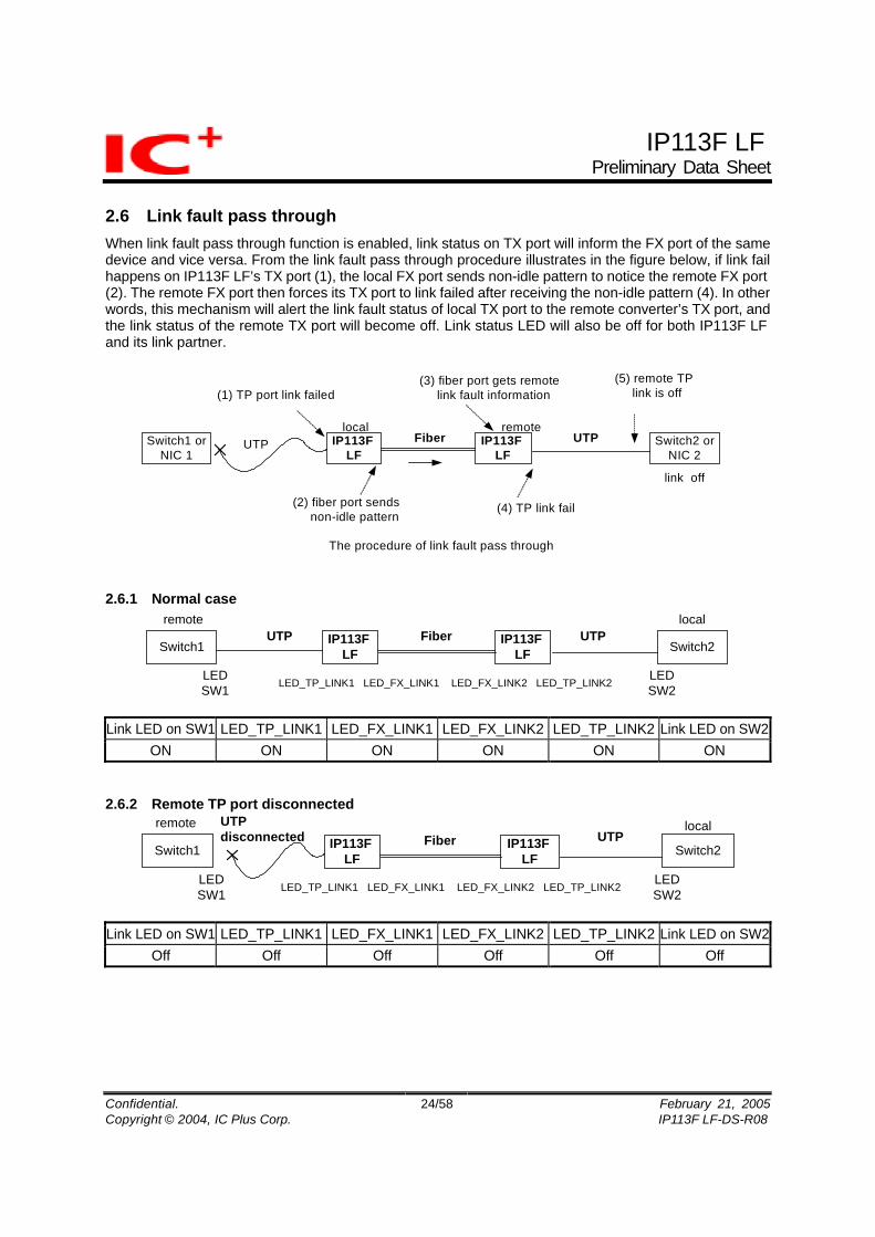
2.6 Link fault pass through When link fault pass through function is enabled, link status on TX port will inform the FX port of the same device and vice versa. From the link fault pass through procedure illustrates in the figure below, if link fail happens on IP113F LF’s TX port (1), the local FX port sends non-idle pattern to notice the remote FX port (2). The remote FX port then forces its TX port to link failed after receiving the non-idle pattern (4). In other words, this mechanism will alert the link fault status of local TX port to the remote converter’s TX port, and the link status of the remote TX port will become off. Link status LED will also be off for both IP113F LF and its link partner.
IP113F LF
IP113F LF
UTP FiberSwitch1 orNIC 1
Switch2 orNIC 2
(1) TP port link failed
link off
The procedure of link fault pass through
(3) fiber port gets remote link fault information
(4) TP link fail
(5) remote TP link is off
(2) fiber port sends non-idle pattern
UTPlocal remote
2.6.1 Normal case
IP113F LF
IP113F LF
UTP UTP FiberSwitch1 Switch2
LED SW1 LED_TP_LINK1 LED_FX_LINK1 LED
SW2
localremote
LED_FX_LINK2 LED_TP_LINK2
Link LED on SW1 LED_TP_LINK1 LED_FX_LINK1 LED_FX_LINK2 LED_TP_LINK2 Link LED on SW2
ON ON ON ON ON ON 2.6.2 Remote TP port disconnected
IP113F LF
IP113F LF
FiberSwitch1 Switch2
LED SW1
LED SW2
localremote
LED_TP_LINK1 LED_FX_LINK1 LED_FX_LINK2 LED_TP_LINK2
UTP UTP disconnected
Link LED on SW1 LED_TP_LINK1 LED_FX_LINK1 LED_FX_LINK2 LED_TP_LINK2 Link LED on SW2
Off Off Off Off Off Off

IP113F LFPreliminary Data Sheet
Confidential. 25/58 February 21, 2005Copyright © 2004, IC Plus Corp. IP113F LF-DS-R08
2.6.3 FX port disconnected
IP113F IP113FUTP UTPFiber
Switch1 Switch2
LEDSW1 LED_TP_LINK1 LED_FX_LINK1 LED
SW2
localremote
LED_FX_LINK2 LED_TP_LINK2
Link LED on SW1 LED_TP_LINK1 LED_FX_LINK1 LED_FX_LINK2 LED_TP_LINK2 Link LED on SW2
Off Off Off Off Off Off 2.6.4 LED diagnostic functions for fault indication LED_TP_LINK LED_FX_LINK LED_FX_SD LED_FX_FEF_DET Status
On On On Off Link ok Flash Flash On Off Link ok & activity
Off Off On Off Remote TP link off Off Off Off Off Fiber RX off, Fiber TX/ RX offOff Off On Flash Fiber TX off
Note Flash: flash, period 100 ms Link fault pass through is enabled. Link fault pass through in FX to FX application
IP113F LF
IP113F LF
UTP 1 UTP 2Fiber 2Switch1 Switch2
LED SW1
LED SW2
localremote
Fiber 1 IP113F LF
LED SW1 and LED SW2 are both off, if either UTP1, Fiber1, Fiber2 or UTP2 is broken and link fault pass through is enabled. That is, if link status is ok on switch port then all segments are guaranteed link good.
IP113F LFPreliminary Data Sheet
Confidential. 26/58 February 21, 2005Copyright © 2004, IC Plus Corp. IP113F LF-DS-R08
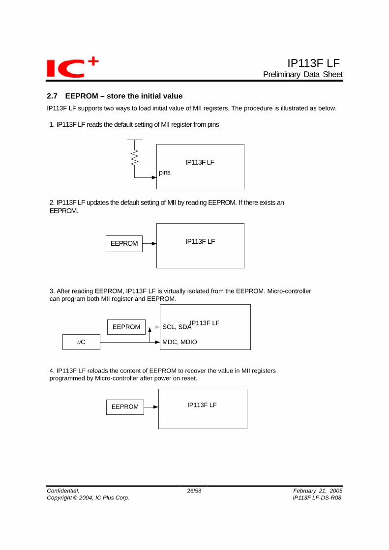
2.7 EEPROM – store the initial value IP113F LF supports two ways to load initial value of MII registers. The procedure is illustrated as below.
IP113F LF
1. IP113F LF reads the default setting of MII register from pins
pins
IP113F LF
2. IP113F LF updates the default setting of MII by reading EEPROM. If there exists an EEPROM.
EEPROM
IP113F LF
3. After reading EEPROM, IP113F LF is virtually isolated from the EEPROM. Micro-controller can program both MII register and EEPROM.
EEPROM
uC MDC, MDIO
SCL, SDA
IP113F LF
4. IP113F LF reloads the content of EEPROM to recover the value in MII registers programmed by Micro-controller after power on reset.
EEPROM

IP113F LFPreliminary Data Sheet
Confidential. 27/58 February 21, 2005Copyright © 2004, IC Plus Corp. IP113F LF-DS-R08
2.8 Auto MDI_MDIX IP113F LF supports auto MDI-MDIX. It is always enabled. The following is its application circuit for auto MDI-MDIX.
IP113F LF
0.1u
RXIP
RXIM
RD +
RD -
transformer
GND
MDI-MDIX
CT
AVCC IP113F LF
0.1u
TXOP
TXOM
TD +
TD -
transformer
GND
MDI-MDIX
CT
AVCC
IP113F LF's application circuit (auto MDI-MDIX on)
50Ω50Ω50Ω50Ω
IP113F LFPreliminary Data Sheet
Confidential. 28/58 February 21, 2005Copyright © 2004, IC Plus Corp. IP113F LF-DS-R08
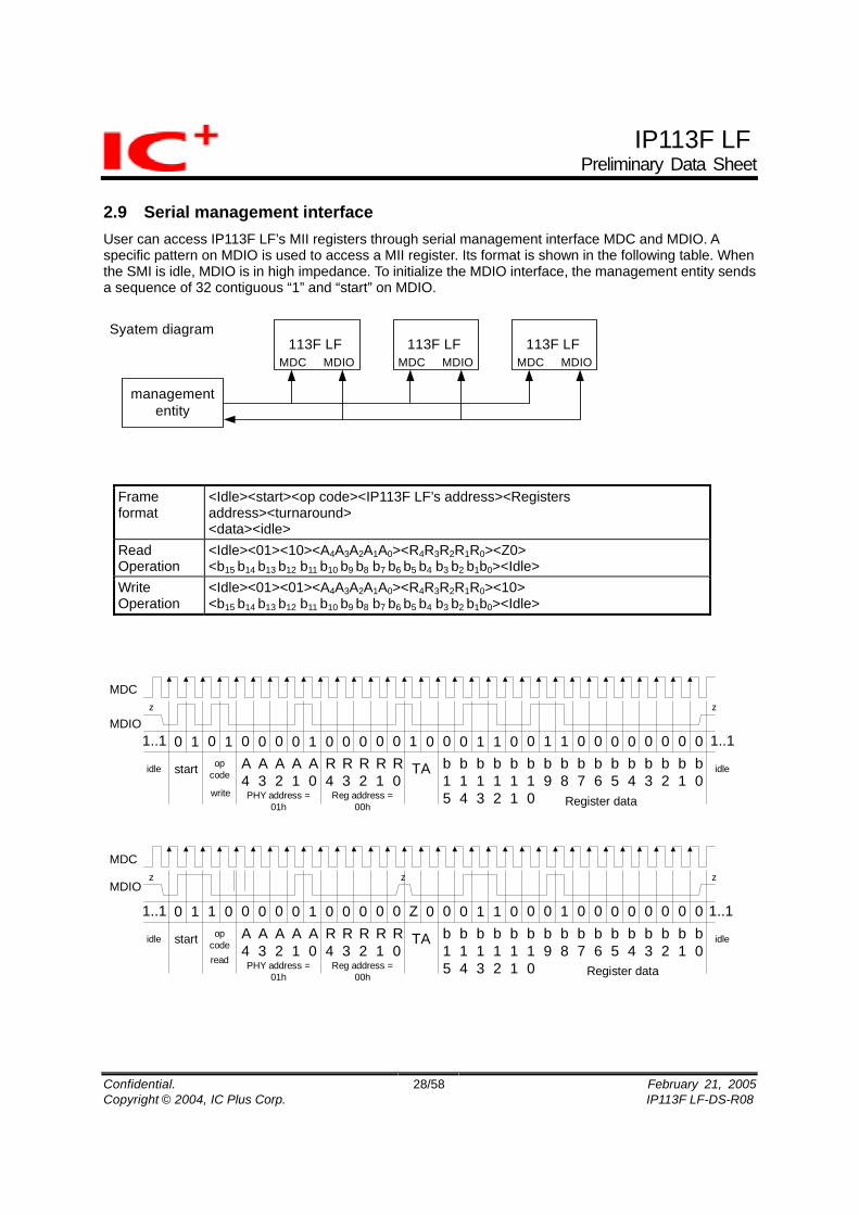
2.9 Serial management interface User can access IP113F LF’s MII registers through serial management interface MDC and MDIO. A specific pattern on MDIO is used to access a MII register. Its format is shown in the following table. When the SMI is idle, MDIO is in high impedance. To initialize the MDIO interface, the management entity sends a sequence of 32 contiguous “1” and “start” on MDIO.
MDIO113F LF
MDC
managemententity
MDIO113F LF
MDCMDIO113F LF
MDC
Syatem diagram
Frame format
<Idle><start><op code><IP113F LF’s address><Registers address><turnaround> <data><idle>
Read Operation
<Idle><01><10><A4A3A2A1A0><R4R3R2R1R0><Z0> <b15 b14 b13 b12 b11 b10 b9 b8 b7 b6 b5 b4 b3 b2 b1b0><Idle>
Write Operation
<Idle><01><01><A4A3A2A1A0><R4R3R2R1R0><10> <b15 b14 b13 b12 b11 b10 b9 b8 b7 b6 b5 b4 b3 b2 b1b0><Idle>
000000001100110001000001000010101..1
idle start opcode
PHY address =01h
Reg address =00h
TA
Register data
b15
b14
b13
b12
b11
b10
b9
b8
b7
b6
b5
b4
b3
b2
b1
b0
idleA4
A3
A2
A1
A0
R4
R3
R2
R1
R0
write
zz
00000000100011000Z00000100000110
idle start opcode
PHY address =01h
Reg address =00h
TA
Register data
b15
b14
b13
b12
b11
b10
b9
b8
b7
b6
b5
b4
b3
b2
b1
b0
idleA4
A3
A2
A1
A0
R4
R3
R2
R1
R0
read
zz z
MDC
MDIO
MDC
MDIO
1..1
1..1
1..1

IP113F LFPreliminary Data Sheet
Confidential. 29/58 February 21, 2005Copyright © 2004, IC Plus Corp. IP113F LF-DS-R08
3. MII registers
Address Register Name Control 0 Control Register NWAY 1 Status Register NWAY 2 PHY identifier Register 1 NWAY 3 PHY identifier Register 2 NWAY 4 AN Advertisement Register NWAY 5 AN Link Partner Base Page Ability Register NWAY 6 AN Expansion Register NWAY 7 (Reserved) 8 (Reserved) 9 (Reserved) 10 (Reserved) 11 (Reserved) 12 (Reserved) 13 (Reserved) 14 (Reserved) 15 (Reserved) 16 Special Control Register NWAY 17 Interrupt Register NWAY 18 Extended Status Register NWAY 19 Statistic Counter Register SWITCH 20 Switch Configuration Register 1 SWITCH 21 Switch Configuration Register 2 SWITCH 22 Local Switch Extended Register SWITCH 23 Link Partner Switch Extended Status Register SWITCH 24 Remote Control Transmit Register 1 RMC 25 Remote Control Transmit Register 2 RMC 26 Remote Control Receive Register 1 RMC 27 Remote Control Receive Register 2 RMC 28 Remote Control Receive Register 3 RMC 29 Remote Control Receive Register 4 RMC 30 Remote Control Receive Register 5 RMC 31 Switch Configuration Register 3 SWITCH
IP113F LFPreliminary Data Sheet
Confidential. 30/58 February 21, 2005Copyright © 2004, IC Plus Corp. IP113F LF-DS-R08
3.1 The basic MII registers
Type Description Type Description R/W Read/Write RC Read and Clear SC Self-Clearing LL Latching Low RO Read Only LH Latching High
Pin(1) The default value is “1” and it depends on the setting of its corresponding pin.
Pin(0) The default value is “0” and it depends on the setting of its corresponding pin.
The basic MII registers 0
MII NAME R/W DESCRIPTION DEFAULTMII control register (address 00h)
0.15 Reset R/W SC
1 = PHY reset 0 = normal operation This bit is self-clearing, IP113F LF will return a value of 1 before reset process is completed, and will not accept any write transaction of MII Management within reset process. Make any change to Auto-Negotiation or speed mode will cause IP113F LF reset again.
0
0.14 Loop back R/W 1 = Loop back mode 0 = normal operation When this bit is set, IP113F LF will be isolated from the network media, and the assertion of TXEN at the MII will not transmit data on the network. All MII transmit data path will return to MII receive data path in response to the assertion of TXEN. MII COL signal will remain de-asserted at all times, unless bit 0.7 (Collision Test) is set. Use has to wait about 100ms for loop back path ready.
0
0.13 Speed Selection RW
1 = 100Mbps 0 = 10Mbps It is valid only if bit 0.12 is set to be 0.
Pin(1)
0.12 Auto-Negotiation Enable
RW
1 = Auto-Negotiation Enable 0 = Auto-Negotiation Disable MII register 16.11 auto-MDI/MDIX should be disabled if auto-negotiation is disabled.
1
0.11 Reserved R/W This bit should be “0” for normal operation. 0 0.10 Isolate R/W 1 = electrically isolate PHY from MII
0 = normal operation When this bit is setting to 1, IP113F LF will be isolated from MII, and not respond to the TXD[3:0] and TXEN and keep CRS, RXDV and RXD[3:0] in high impedance, but will respond to management transactions.
0

IP113F LFPreliminary Data Sheet
Confidential. 31/58 February 21, 2005Copyright © 2004, IC Plus Corp. IP113F LF-DS-R08
MII NAME R/W DESCRIPTION DEFAULT
MII control register (address 00h) 0.9 Restart Auto-
Negotiation RW
1 = re-starting Auto-Negotiation 0 = Auto-Negotiation re-start complete Setting this bit to logic high will cause IP113F LF to restart an Auto-Negotiation cycle, but depend on the value of bit 0.12 (Auto-Negotiation Enable). If bit 0.12 is cleared then this bit has no effect, and change to Read Only. When an Auto-Negotiation cycle is being processed, write 0 into this bit has no effect. This bit is self-clearing after Auto-Negotiation process is completed.
0
0.8 Duplex mode R/W
1 = full duplex 0 = half duplex It is valid only if bit 0.12 is set to be 0.
Pin(1)
0.7 Collision test enable R/W 1 = enable the collision test 0 = disable the collision test If setting this bit to logic 1, when MII TXEN signal is asserted, IP113F LF will assert the MII COL signal within 512BT (Bit Time, depend on 10Mbps or 100Mbps). When MII TXEN is de-asserted, then TP110 will assert MII COL signal within 4BT. Clearing this bit to logic 0 for normal operation
0
0[6:0] Reserved R/W Write as 0, ignore on read -

IP113F LFPreliminary Data Sheet
Confidential. 32/58 February 21, 2005Copyright © 2004, IC Plus Corp. IP113F LF-DS-R08
The basic MII registers 1
MII NAME R/W DESCRIPTION DEFAULTMII status register (address 01h)
1.15 100Base-T4 capable
RO 1 = 100Base-T4 capable 0 = not 100Base-T4 capable IP113F LF does not support 100Base-T4. This bit is fixed to be 0.
0
1.14 100Base-X full duplex Capable
RO 1 = 100Base-X full duplex capable 0 = not 100Base-X full duplex capable The default of this bit will change depend on the external setting of IP113F LF. If external pin setting without 100Base-X full duplex support, then this bit will change default to logic 0.
1
1.13 100Base-X half duplex Capable
RO 1 = 100Base-X half duplex capable 0 = not 100Base-X half duplex capable The default of this bit will change depend on the external setting of IP113F LF. If external pin setting without 100Base-X half duplex support, then this bit will change default to logic 0
1
1.12 10Base-T full duplex Capable
RO 1 = 10Base-T full duplex capable 0 = not 10Base-T full duplex capable The default of this bit will change depend on the external setting of IP113F LF. If external pin setting without 100Base-T full duplex support, then this bit will change default to logic 0
1
1.11 10Base-T half duplex Capable
RO 1 = 10Base-T half duplex capable 0 = not 10Base-T half duplex capable The default of this bit will change depend on the external setting of IP113F LF. If external pin setting without 100Base-X full duplex support, then this bit will change default to logic 0
1
1[10:7] Reserved RO Ignore on read - 1.6 MF preamble
Suppression RO 1 = preamble may be suppressed
0 = preamble always required 1
1.5 Auto-Negotiation Complete
RO 1 = Auto-Negotiation complete 0 = Auto-Negotiation in progress When read as logic 1, indicates that the Auto-Negotiation process has been completed, and the contents of register 4, 5, 6 and 7 are valid. When read as logic 0, indicates that the Auto-Negotiation process has not been completed, and the contents of register 4, 5, 6 and 7 are meaningless. If Auto-Negotiation is disabled (bit 0.12 set to logic 0), then this bit will always read as logic 0.
0

IP113F LFPreliminary Data Sheet
Confidential. 33/58 February 21, 2005Copyright © 2004, IC Plus Corp. IP113F LF-DS-R08
The basic MII registers 1(continued)
MII NAME R/W DESCRIPTION DEFAULTMII status register (address 01h)
1.4 Remote fault RO LH
1 = remote fault detected 0 = not remote fault detected When read as logic 1, indicates that IP113F LF has detected a remote fault condition. This bit is set until remote fault condition gone and before reading the contents of the register. This bit is cleared after IP113F LF reset.
0
1.3 Auto-Negotiation Ability
RO 1 = Auto-Negotiation capable 0 = not Auto-Negotiation capable When read as logic 1, indicates that IP113F LF has the ability to perform Auto-Negotiation. The value of this bit will depend on the external mode setting of IP113F LF operation mode.
1
1.2 Link Status RO LL
1 = Link Pass 0 = Link Fail When read as logic 1, indicates that IP113F LF has determined a valid link has been established. When read as logic 0, indicates the link is not valid. This bit is cleared until a valid link has been established and before reading the contents of this registers.
0
1.1 Jabber Detect RO LH
1 = jabber condition detected 0 = no jabber condition detected When read as logic 1, indicates that IP113F LF has detected a jabber condition. This bit is always 0 for 100Mbps operation and is cleared after IP113F LF reset. This bit is set until jabber condition is cleared and reading the contents of the register.
0
1.0 Extended capability RO 1 = Extended register capabilities 0 = No extended register capabilities IP113F LF has extended register capabilities.
1

IP113F LFPreliminary Data Sheet
Confidential. 34/58 February 21, 2005Copyright © 2004, IC Plus Corp. IP113F LF-DS-R08
The basic MII registers 2 , 3
MII NAME R/W DESCRIPTION DEFAULTPHY Identifier (address 02h) 2[15:0] PHY identifier RO IP113F LF OUI (Organizationally Unique Identifier)
ID, the msb is 3rd bit of IP113F LF OUI ID, and the lsb is 18th bit of IP113F LF OUI ID. IP113F LF OUI is 0090C3.
0243h
MII NAME R/W DESCRIPTION DEFAULTPHY Identifier (address 03h) 3[15:10] PHY identifier RO IP113F LF OUI ID, the msb is 19th bit of IP113F
LF OUI ID, and lsb is 24th bit of IP113F LF OUI ID. 3h
3[9:4] Manufacture’s Model Number
RO TP110 model number 5h
3[3:0] Revision Number RO IP113F LF revision number 0
IP113F LFPreliminary Data Sheet
Confidential. 35/58 February 21, 2005Copyright © 2004, IC Plus Corp. IP113F LF-DS-R08
The basic MII registers 4
MII NAME R/W DESCRIPTION DEFAULTAuto-Negotiation Advertisement register (address 04h)
4.15 Next Page RO 1 = Next Page ability is supported 0 = Next Page ability is not supported IP113F LF does not support next page, this bit is fixed to be 0.
0
4.14 Reserved RW Reserved by IEEE, write as 0, ignore on read 0 4.13 Remote Fault R/W 1 = Advertises that this device has detected a
remote fault 0 = No remote fault detected
0
4[12:11] Reserved RO Reserved for future IEEE use, write as 0, ignore on read
0
4.10 Pause RW 1 = Advertises that this device has implemented pause function
0 = No pause function supported
Pin(1)
4.9 100BASE-T4 RW 1 = 100BASE-T4 is supported 0 = 100BASE-T4 is not supported
0
4.8 100BASE-TX full duplex
R/W 1 = 100BASE-TX full duplex is supported 0 = 100BASE-TX full duplex is not supported
Pin(1)
4.7 100BASE-TX R/W 1 = 100BASE-TX is supported 0 = 100BASE-TX is not supported
Pin(1)
4.6 10BASE-T full duplex
R/W 1 = 10BASE-T full duplex is supported 0 = 10BASE-T full duplex is not supported
Pin(1)
4.5 10BASE-T R/W 1 = 10BASE-T is supported 0 = 10BASE-T is not supported
Pin(1)
4[4:0] Selector Field RO Use to identify the type of message being sent by Auto-Negotiation.
00001

IP113F LFPreliminary Data Sheet
Confidential. 36/58 February 21, 2005Copyright © 2004, IC Plus Corp. IP113F LF-DS-R08
The basic MII registers 5
MII NAME R/W DESCRIPTION DEFAULTLink partner ability register (address 05h) Base Page
5.15 Next Page RO 1 = Next Page ability is supported by link partner 0 = Next Page ability is not supported by link partner
0
5.14 Acknowledge RO 1 = Link partner has received the ability data word 0 = Not acknowledge
0
5.13 Remote Fault RO 1 = Link partner indicates a remote fault 0 = No remote fault indicate by link partner If this bit is set to logic 1, then bit 1.4 (Remote fault) will set to logic 1.
0
5[12:10] Reserved RO Reserved by IEEE for future use, write as 0, read as 0.
0
5.9 100BASE-T4 RO 1 = Link partner support 100BASE-T4 0 = Link partner is not support 100BASE-T4
0
5.8 100BASE-TX full duplex
RO 1 = Link partner support 100BASE-TX full duplex 0 = Link partner is not support 100BASE-TX full
duplex
0
5.7 100BASE-TX RO 1 = Link partner support 100BASE-TX 0 = Link partner is not support 100BASE-TX
0
5.6 10BASE-T full duplex
RO 1 = Link partner support 10BASE-T full duplex 0 = Link partner is not support 10BASE-T full duplex
0
5.5 10BASE-T RO 1 = Link partner support 10BASE-T 0 = Link partner is not support 10BASE-T
0
5[4:0] Selector Field RO Protocol selector of the link partner 00000

IP113F LFPreliminary Data Sheet
Confidential. 37/58 February 21, 2005Copyright © 2004, IC Plus Corp. IP113F LF-DS-R08
The basic MII registers 6
MII NAME R/W DESCRIPTION DEFAULTAuto-Negotiation Expansion register (address 06h) 6[15:5] Reserved RO Reserved by IEEE, writes as 0, ignore on read. 0
6.4 Parallel Detection Fault
RO LH
1 = A fault has been detected via Parallel Detection function
0 = A fault has not detected via Parallel Detection function
0
6.3 Link Partner Next Page Able
RO 1 = Link Partner is Next Page able 0 = Link Partner is not Next Page able
0
6.2 Next Page Able RO 1 = Local Device is Next Page able 0 = Local Device is not Next Page able
1
6.1 Page Received RO LH
1 = A New Page has been received 0 = A New Page has not been received
0
6.0 Link Partner Auto-Negotiation Able
RO 1 = Link Partner is Auto-Negotiation able 0 = Link Partner is not Auto-Negotiation able
0

IP113F LFPreliminary Data Sheet
Confidential. 38/58 February 21, 2005Copyright © 2004, IC Plus Corp. IP113F LF-DS-R08
3.2 Extended MII registers and EEPROM registers
MII ROM NAME R/W DESCRIPTION DEFAULTEEPROM enable register 0 (EEPROM register 00D)
-- 0[7:0] RO EEPROM enable register 0 This register should be filled with 55. IP113F LF will examine the specified pattern to confirm if there is a valid EEPROM.
55
MII ROM NAME R/W DESCRIPTION DEFAULTEEPROM enable register 1 (EEPROM register 01D)
-- 1[7:0] RO EEPROM enable register 1 This register should be filled with AA. IP113F LF will examine the specified pattern to confirm if there is a valid EEPROM. The initial setting is updated with the content of EEPROM only if the specified pattern 55AA is found.
AA

IP113F LFPreliminary Data Sheet
Confidential. 39/58 February 21, 2005Copyright © 2004, IC Plus Corp. IP113F LF-DS-R08
Extended MII registers and EEPROM registers 16
MII ROM NAME R/W DESCRIPTION DEFAULTSpecial control register (16D)
16.0 -- Reserved This bit should be “0” for normal operation. 0 16.1 -- Reserved This bit should be “0” for normal operation. 0 16.2 -- Reserved This bit should be “0” for normal operation. 0 16.3 -- mr_bypass_scramble R/W Bypass PCS scrambler (It is valid only if
16.15=1.) 1: bypass scrambler, 0: not bypass (default) This bit should be “0” for normal operation.
0
16.4 -- mr_bypass_100x _coder
R/W Bypass PCS 4B/5B coder (It is valid only if 16.15=1.) 1: bypass 4B/5B, 0: not bypass (default) This bit should be “0” for normal operation.
0
16.5 -- mr_bypass_dsp_rst R/W Bypass DSP re-start function in PCS 1: bypass DSP re-start, 0: not bypass (default) This bit should be “0” for normal operation.
0
16.6 -- mr_tx_nlp_disable R/W 10Mb transmit NLP enable 1: enable (default), 0:disable This bit should be “1” for normal operation.
0
16.7 -- mr_analog_pwsv _disable
R/W Analog power save mode disable 1: disable, 0: enable (default) The default value is recommended to adopt.
0
16.8 -- mr_fef_disable R/W Far-End-Fault function disable 1: disable, 0: enable (default) The default value is recommended to adopt.
0
16.9 -- mr_jabber_enable R/W Jabber function enable 1: enable, 0:disable (default) The default value is recommended to adopt.
0
16.10 -- mr_heart_beat _enable
R/W Heart Beat function enable 1: enable, 0:disable (default) The default value is recommended to adopt.
0
16.11 -- mr_auto_cross _disable
R/W Auto Crossover function disable 1: disable, 0: enable (default) It should be disabled if MII register 0.12 auto-negotiation is disabled.
0
16.12 -- Reserved This bit should be “0” for normal operation. 0 16.13 -- Reserved This bit should be “0” for normal operation. 0 16.14 -- Reserved R/W 0 16.15 -- Reserved This bit should be “0” for normal operation. 0
IP113F LFPreliminary Data Sheet
Confidential. 40/58 February 21, 2005Copyright © 2004, IC Plus Corp. IP113F LF-DS-R08
Extended MII registers and EEPROM registers 17
MII ROM NAME R/W DESCRIPTION DEFAULTInterrupt register (17D)
17.0 -- intr_link RO RC
Link status change It is logic “1” when link status changes on TP port and it will active interrupt pin. It is self-clear after reading the register. 1: link status change Interrupt occur, 0: no interrupt
0
17.1 -- intr_duplex RO RC
Duplex mode change It is logic “1” when duplex status changes on TP port and it will active interrupt pin. It is self-clear after reading the register. 1: duplex status change Interrupt occur, 0: no interrupt
0
17.2 -- intr_speed RO RC
Speed mode change It is logic “1” when speed changes on TP port and it will active interrupt pin. It is self-clear after reading the register. 1: speed change interrupt occur, 0: no interrupt
0
17.3 -- intr_mf_rx_indicate RO RC
Undefined maintenance frame receive indication It is logic “1” when an undefined maintenance frame is received and it will active interrupt pin. An undefined maintenance frame is a frame, which can’t be recognized by IP113F LF. It is self-clear after reading the register. 1: Rx maintenance frame interrupt occur, 0: no interrupt
0
17.4 -- intr_cnt_overflow RO RC
Statistic counter overflow It is logic “1” when statistic counter is overflow and it will active interrupt pin. It is self-clear after reading the register. 1: counter overflow interrupt occur, 0: no interrupt
0
17.5 -- intr_status RO RC
Interrupt status It is logic “OR” of bit 17.0~17.4. 1: any interrupt occur, 0: no interrupt
0
17.6 -- Intr_pwabn RO RC
Power abnormal It is logic “1” when 113F receives a maintenance frame with link partner’s power abnormal message and it will active interrupt pin. It is self-clear after reading the register. 1: remote link partner power abnormal 0: nothing happen
0

IP113F LFPreliminary Data Sheet
Confidential. 41/58 February 21, 2005Copyright © 2004, IC Plus Corp. IP113F LF-DS-R08
Extended MII registers and EEPROM registers 17(continued)
MII ROM NAME R/W DESCRIPTION DEFAULTInterrupt register (17D)
17.7 -- Intr_pwabn_en RW Remote LP power abnormal interrupt enable A mask for bit 17.6. 1: not mask interrupt 0: mask interrupt
0
17.8 -- intr_link_mask RW Mask TP port link change Interrupt A mask for bit 17.0. 1: mask, 0: not mask (default)
1
17.9 -- intr_duplex_mask RW Mask TP port duplex mode change Interrupt A mask for bit 17.1. 1: mask interrupt (default), 0: not mask
1
17.10 -- intr_speed_mask RW Mask TP port speed mode change Interrupt A mask for bit 17.2. 1: mask interrupt (default), 0: not mask
1
17.11 -- intr_mf_rx_indc _mask
RW Mask maintenance frame receive indication Interrupt A mask for bit 17.3. 1: mask interrupt (default), 0: not mask
1
17.12 -- intr_cnt_ov_mask RW Mask Statistic counter overflow Interrupt A mask for bit 17.4. 1: mask interrupt (default), 0: not mask
1
17.13 -- intr_all_mask RW Mask all Interrupt It enables the all mask bits 17.7~17.12. 1: mask interrupt (default), 0: not mask
1
17[15:14] -- Reserved RW 0
IP113F LFPreliminary Data Sheet
Confidential. 42/58 February 21, 2005Copyright © 2004, IC Plus Corp. IP113F LF-DS-R08
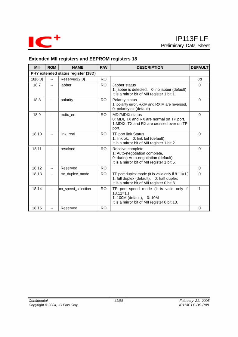
Extended MII registers and EEPROM registers 18
MII ROM NAME R/W DESCRIPTION DEFAULTPHY extended status register (18D) 18[6:0] -- Reserved[2:0] RO 8d 18.7 -- jabber RO Jabber status
1: jabber is detected, 0: no jabber (default) It is a mirror bit of MII register 1 bit 1.
0
18.8 -- polarity RO Polarity status 1: polarity error, RXIP and RXIM are reversed, 0: polarity ok (default)
0
18.9 -- mdix_en RO MDI/MDIX status 0: MDI, TX and RX are normal on TP port. 1:MDIX, TX and RX are crossed over on TP port.
0
18.10 -- link_real RO TP port link Status 1: link ok, 0: link fail (default) It is a mirror bit of MII register 1 bit 2.
0
18.11 -- resolved RO Resolve complete 1: Auto-negotiation complete, 0: during Auto-negotiation (default) It is a mirror bit of MII register 1 bit 5.
0
18.12 -- Reserved RO 0 18.13 -- mr_duplex_mode RO TP port duplex mode (It is valid only if 8.11=1.)
1: full duplex (default), 0: half duplex It is a mirror bit of MII register 0 bit 8.
0
18.14 -- mr_speed_selection RO TP port speed mode (It is valid only if 18.11=1.) 1: 100M (default), 0: 10M It is a mirror bit of MII register 0 bit 13.
1
18.15 -- Reserved RO 0

IP113F LFPreliminary Data Sheet
Confidential. 43/58 February 21, 2005Copyright © 2004, IC Plus Corp. IP113F LF-DS-R08
Extended MII registers and EEPROM registers 19
MII ROM NAME R/W DESCRIPTION DEFAULTStatistic counter registers (MII register 19D)
Statistic Counter [11:0] The statistic counter maintains some kinds of statistic information. Before reading the statistic counter, user has to select one counter by writing MII register 19[14:12] cnt_index[2:0]. The relationship between cnt_index and its corresponding counter is shown in the following table. Cnt_index Content of statistic counter[11:0] 3'b000 Received packet count on TP port 3'b001 Received CRC error count on TP
port 3'b010 Drop packet count on TP port 3'b011 Collision event count on TP port 3'b100 Received packet count on fiber port 3'b101 Received CRC error count on fiber
port 3'b110 Drop packet count on fibe port
19[11:0] -- mg_statistic_cnt[11:0] RO
3'b111 Collision event count on fiber port
0
19[14:12] -- cnt_index[2:0] RW The current counter index A counter index to select one counter before reading MII register 19[11:0]
0
19.15 -- cnt_loop_en RW The counter index loop enable 1: MII register 19[14:12] cnt_index[2:0] is increased by one automatically whenever the MII register 19 is read. Cnt_index[2:0] is turned arounf to “000” when it reaches to “111” and is read. 0: cnt_index[2:0] is not increased when MII register 19 is read.
1

IP113F LFPreliminary Data Sheet
Confidential. 44/58 February 21, 2005Copyright © 2004, IC Plus Corp. IP113F LF-DS-R08
Extended MII registers and EEPROM registers 20
MII ROM NAME R/W DESCRIPTION DEFAULTSwitch configuration register 1 (MII register 20D, EEPROM register 02~03D)
20.0 2.0 Reserved 0 20.1 2.1 direct_wire R/W Please see pin description of DIRECT_WIRE
for more detail information. This bit overwrites the setting on pin 22 DIRECT_WIRE.
Pin (0)
20.2 2.2 fast_fwd R/W Please see pin description of FAST_FWD for more detail information. This bit overwrites the setting on pin 23 FAST_FWD.
Pin (0)
20.3 2.3 mg_pass_fragment _en
R/W Pass fragment packet, which is longer than 7 bytes and shorter than 64bytes1: pass fragment 0: not pass fragment
0
20.4 2.4 mg_col16_drop_en R/W Collision 16 times drop enable A port drops a transmission packet if it experiences 16 consecutive collisions. 1: enable 0: disable
0
20.5 2.5 mg_col_backoff_en R/W Collision back-off enable 1: back off after collision 0: not back off after collision This bit should be “1” for normal operation.
1
20.6 2.6 Reserved R/W It must be 0. 0 20.7 2.7 p01_mg_backpress
_en R/W TP port backpressure enable
Backpressure is flow control for half duplex operation 1: backpressure enable 0: backpressure disable
1
20.8 3.0 mg_rem_ctrl_en R/W Remote control enable 1: ability enable. IP113F LF is capable of
transmission and receiving maintenance frame to perform remote control.
0: ability disable. IP113F LF is not capable of transmission and receiving maintenance frame to perform remote control.
1
20.9 3.1 mg_auto_tx_mf_en R/W Auto send status frame to link partner through fiber port (AUTO_SEND) 1: auto send indication maintenance frame 0: disable auto send function This bit overwrites the setting on pin 25 AUTO_SEND. Please see pin description of AUTO_SEND for more detail information.
Pin (0)

IP113F LFPreliminary Data Sheet
Confidential. 45/58 February 21, 2005Copyright © 2004, IC Plus Corp. IP113F LF-DS-R08
Extended MII registers and EEPROM registers 20(continued)
MII ROM NAME R/W DESCRIPTION DEFAULTSwitch configuration register 1 (MII register 20D, EEPROM register 02~03D) 20.10 3.2 mg_auto_tx_ttc
_content R/W The format of auto send status frame
1: TTC (TS-1000) IP113F LF performs auto send functions with the frame format defined in TS-1000. 0: ICPLUS IP113F LF performs auto send functions with the ICPLUS proprietary frame format. The frame format is similar to the one defined in TS-1000 except the bit definition of S[15:0]. S[15:0] carries the content of MII register 22[15:0] local MC extended register. IP113F LF uses the frame to indicate its status to its link partner. The link partner, another IP113F LF, stores the information in the S[15:0] field of the frame to its MII register 23 after receiving the frame.
1
20.11 3.3 mg_sd_off_way R/W Informing way for optical receiving SD off 1: IP113F LF uses far end fault pattern to
notify the link partner SD off information through fiber port.
0: IP113F LF uses maintenance frame to notify the link partner SD off information through fiber port.
1
20.12 3.4 Reserved R/W This bit should be “0” for normal operation. 1 20.13 3.5 tp_force R/W This pin overwrites the setting on pin 26
TP_FORCE. Please see pin description of TP_FORCE for more detail information.
Pin (0)
20.14 3.6 mg_receive_en R/W TP receive enable 1: TP port can receive packet 0: TP port drop all received packet This bit should be “1” for normal operation.
1
20.15 3.7 p02_receive_on RO LL RC
Fiber port receive path ready 1: Fiber port receive path is ready (SD is on and normal IDLE pattern received) 0: Fiber port receive path is not ready
0

IP113F LFPreliminary Data Sheet
Confidential. 46/58 February 21, 2005Copyright © 2004, IC Plus Corp. IP113F LF-DS-R08
Extended MII registers and EEPROM registers 21
MII ROM NAME R/W DESCRIPTION DEFAULTSwitch configuration register 2 (MII register 21D, EEPROM register 04~05D) The register is for testing only. Access to this register may cause malfunction. 21[7:0] 4[7:0] Reserved R/W The default value must be adopted if uses
use an EEPORM. 120d
21[15:8] 5[7:0] Reserved R/W The default value must be adopted if uses use an EEPORM.
120d

IP113F LFPreliminary Data Sheet
Confidential. 47/58 February 21, 2005Copyright © 2004, IC Plus Corp. IP113F LF-DS-R08
Extended MII registers and EEPROM registers 22
MII ROM NAME R/W DESCRIPTION DEFAULTLocal MC extended register (MII register 22D, EEPROM register 06~07D)
22.0 6.0 mg_loopback_en R/W TP port loop-back test enable 1: loop back mode 0: normal mode It is a mirror bit of MII register 0 bit 14.
0
22.1 6.1 mg_status_rpt_en RO TP port status (link, speed, duplex) available 1: TP status is valid 0: TP status is not ready
0
22.2 6.2 p01_mg_auto_neg _en
R/W TP port auto-negotiation enable 1: TP auto-negotiation enable 0: TP auto-negotiation disable It is a mirror bit of MII register 0 bit 12.
1
22.3 6.3 p01_mg_speed _mode
R/W TP port speed selection 1: 100M, 0:10M It is a mirror bit of MII register 0 bit 13.
Pin (1)
22.4 6.4 p01_mg_duplex _mode
R/W TP port duplex mode selection 1: full duplex, 0:half duplex It is a mirror bit of MII register 0 bit 8. This bit overwrites the setting on pin 30 DUPLEX_MODE.
Pin (0)
22.5 6.5 p01_mg_flow_ctrl_ en
R/W TP port flow control selection 1: on, 0:off It is a mirror bit of MII register 4 bit 10. This bit overwrites the setting on pin 29 X_EN for TP port.
Pin (1)
22.6 6.6 p01_mg_link_status RO TP port link status off 1: link off, 0: link on
1
22.7 6.7 p02_mg_flow_ctrl_ en
R/W Fiber port flow control/backpressure enable 1: enable, 0: disable This bit overwrites the setting on pin 29 X_EN for fiber port.
Pin (1)
22.8 7.0 p02_mg_duplex _mode
R/W Fiber port duplex mode 1: full duplex, 0:half duplex This bit overwrites the setting on pin 36 FX_FULL.
Pin(1)
22.9 7.1 p02_mg_link_status RO LL RC
Fiber port signal detect (power) 1: Fiber SD has been low since last read 0: Fiber SD is O.K. It is self-set after reading.
1
22.10 7.2 p02_mg_fef_detect RO LH RC
Fiber port Far-End-Fault detect 1: FEF has been detected since last read 0: no FEF pattern detected It is self-clear after reading.
0

IP113F LFPreliminary Data Sheet
Confidential. 48/58 February 21, 2005Copyright © 2004, IC Plus Corp. IP113F LF-DS-R08
Extended MII registers and EEPROM registers 22(continued)
MII ROM NAME R/W DESCRIPTION DEFAULTLocal MC extended register (MII register 22D, EEPROM register 06~07D)
TP port input Rate Control IP113F LF limits the input traffic of TP port. Traffic 10M mode 100M mode 00 10Mbps 100Mbps 01 2.5Mbps 25Mbps 10 5Mbps 50Mbps
22[12:11] 7[4:3] p01_mg_throttle _confg
R/W
11 7.5Mbps 75Mbps
00
TP port output Rate Control IP113F LF limits the output traffic of TP port. Traffic 10M mode 100M mode 00 10Mbps 100Mbps 01 2.5Mbps 25Mbps 10 5Mbps 50Mbps
22[14:13] 7[6:5] p01_mg_throttle _confg
R/W
11 7.5Mbps 75Mbps
00
22.15 7.7 mg_link_pass_en R/W Link Fault Pass through enable (LFP) 1: enable, 0: disable This bit overwrites the setting on pin 21 LFP.
Pin (0)

IP113F LFPreliminary Data Sheet
Confidential. 49/58 February 21, 2005Copyright © 2004, IC Plus Corp. IP113F LF-DS-R08
Extended MII registers and EEPROM registers 23
MII ROM NAME R/W DESCRIPTION DEFAULTLink partner MC extended status register (MII register 23D)
23.0 -- lp_loopback_en RO Loop-back enable of remote LP 1: Link partner’s fiber port is in loop back
mode. Its fiber port will forward all receiving frames from FXRDP/M to FXTDP/M..
0: Link partner’s fiber port is in normal mode
0
23.1 -- lp_status_rpt_en RO Option B support 1: Link partner supports TS-1000 option B 0: not support
0
23.2 -- lp_tp_autoneg_en RO TP port auto-negotiation enable 1: Link supports aut0-negotuation, 0: Link partner doesn’t support auto-negotiation.
0
23.3 -- lp_tp_speed_mode RO TP port speed of link partner 1: 100M, 0:10M
0
23.4 -- lp_tp_duplex_mode RO TP port duplex mode of link partner 1: full duplex, 0: half duplex
0
23.5 -- lp_tp_flow_ctrl_en RO TP port flow control of link partner. 1: flow control enable 0: flow control disable This bit is valid only if MII register 20 bit10 is set to be 0.
0
23.6 -- lp_tp_link_off RO TP port link status of link partner 1: link off, 0:link on
1
23.7 -- lp_fb_flow_ctrl_en RO Fiber port flow control/backpressure of link partner This bit is valid only if MII register 20 bit10 is set to be 0. 1: flow control enable 0: flow control disable
0
23.8 -- lp_fb_duplex_mode RO Fiber port duplex mode of link partner 1: full duplex, 0: half duplex This bit is valid only if MII register 20 bit10 is set to be 0.
0
23.9 -- lp_fb_link_status RO Fiber port signal detect status of link partner 1: off, 0: on This bit is valid only if MII register 20 bit10 is set to be 0.
0

IP113F LFPreliminary Data Sheet
Confidential. 50/58 February 21, 2005Copyright © 2004, IC Plus Corp. IP113F LF-DS-R08
Extended MII registers and EEPROM registers 23(continued)
MII ROM NAME R/W DESCRIPTION DEFAULTLink partner MC extended status register (MII register 23D) 23.10 -- reserved RO 0 23.11 -- lp_power_abnormal RO Power status of link partner
1: power abnormal 0: power O.K.
0
23.12 -- lp_mc_failed RO MC failed 1: link partner malfunctions 0: link partner is normal
0
23.13 -- lp_sd_off_way RO Link Partner informing way of SD off 1: Link partner sends far end fault pattern
when its SD is off. 0: Link partner sends maintenance frame
when its SD is off.
1
23.14 -- lp_multi_tp_port RO MC support multi-port UTP 1: Link partner supports more than one TP
port 0: Link partner supports one TP port
0
23.15 -- mg_link_pass_en RO Link Fault Pass through enable 1: Link partner supports Link Fault Pass
Through function 0: Link partner doesn’t support Link Fault
Pass Through function This bit is valid only if MII register 20 bit10 is set to be 0.
0

IP113F LFPreliminary Data Sheet
Confidential. 51/58 February 21, 2005Copyright © 2004, IC Plus Corp. IP113F LF-DS-R08
Extended MII registers and EEPROM registers 24
MII ROM NAME R/W DESCRIPTION DEFAULTRemote control Transmit register 1 (MII register 24D)
24.0 -- mg_rem_tx_code R/W Remote control frame send trigger 1: command IP113F LF to send a
maintenance frame 0: does not command IP113F LF to send a
maintenance frame If user wants to send another maintenance frame, he has to write “1” to this bit again.
0
24.1 -- mg_rem_tx_code R/W Transmitted maintenance direction discriminator C1
It is C1 field of a maintenance frame. 0: upstream 1: downstream
0
24[3:2] -- mg_rem_tx_code R/W Transmitted maintenance frame command discriminator C3~C2
It is C[3:2] field of a maintenance frame. 01: request 11: acknowledge 10: Indication 00: reserved
00
Transmitted maintenance frame control signals C15~C8
It is C[15:8] field of a maintenance frame. Bit11(C15) ……..bit4(C8) Function 0 0 0 0 0 0 01 Loop test start 0 0 0 0 0 0 00 Loop test finished 0 0 0 0 0 0 10 Status indication Address [4:0] R/W 11 R/W link partner’s
registers
24[11:4] -- mg_rem_tx_code R/W
Note: R/W: 0: read, 1: write A[4:0]: register address
8’b0
24[15:12] -- Reserved

IP113F LFPreliminary Data Sheet
Confidential. 52/58 February 21, 2005Copyright © 2004, IC Plus Corp. IP113F LF-DS-R08
Extended MII registers and EEPROM registers 25
MII ROM NAME R/W DESCRIPTION DEFAULTRemote control Transmit register 2 (MII register 25D) 25[15:0] -- mg_rem_wt_data R/W Remote control write data
If a remote write command is issued, that is, MII register 24[6:4] is programmed as 111. The content in this register will be embedded into S[15:0] of a maintenance and is sent to the link partner. The link partner, an IP113F LF, will update the addressed MII register with the value defined in this register after receiving the remote write command.
16’b0

IP113F LFPreliminary Data Sheet
Confidential. 53/58 February 21, 2005Copyright © 2004, IC Plus Corp. IP113F LF-DS-R08
Extended MII registers and EEPROM registers 26
MII ROM NAME R/W DESCRIPTION DEFAULTRemote control Receive register 1 (MII register 26D)
26.0 -- mg_rem_rx_code RO RC
Receive an acknowledge maintenance, that is field C[2:3]=11, or undefined maintenance frame. 1: IP113F LF receives a response
(acknowledge) maintenance frame or undefined maintenance frame.
0: no response (acknowledge) maintenance frame or undefined maintenance frame received. User can poll this bit to make sure if there is an acknowledge maintenance frame or an undefined maintenance frame is received. It is a read and auto-clear bit. Note: register 26~30 will be updated only when this bit is 1.
0
26.1 -- mg_rem_rx_code RO Direction discriminator C1 of a received maintenance frame.
0
26[3:2] -- mg_rem_rx_code RO Command discriminator C3~C2 of a received maintenance frame.
00
26[11:4] -- mg_rem_rx_code RO control signals C15~C8 of a received maintenance frame.
8’b0
26[12] -- mg_rem_rx_code RO RC
Received maintenance frame CRC error 1: received a maintenance frame with CRC
error. 0: received a maintenance frame with
correct CRC . It is a read and auto-clear bit.
26[15:13] -- Reserved

IP113F LFPreliminary Data Sheet
Confidential. 54/58 February 21, 2005Copyright © 2004, IC Plus Corp. IP113F LF-DS-R08
Extended MII registers and EEPROM registers 27,28,29,30
MII ROM NAME R/W DESCRIPTION DEFAULTRemote control Receive register 2 (MII register 27D) 27[15:0] -- mg_rem_rd_data RO Remote read data
The link partner will send out a maintenance frame carrying remote-read data if IP113F LF issues a remote-read command by sending a maintenance frame. It is derived from the S[15:0] field of a received maintenance frame sent by the link partner.
16’b0
MII ROM NAME R/W DESCRIPTION DEFAULTRemote control Receive register 3 (MII register 28D) 28[15:0] -- mg_rem_rd_data RO Vender message M0~M15
The M[15:0] field of a received maintenance frame sent by the link partner.
16’b0
MII ROM NAME R/W DESCRIPTION DEFAULTRemote control Receive register 4 (MII register 29D) 29[15:0] -- mg_rem_rd_data RO Vender message M16~M31
The M[31:16] field of a received maintenance frame sent by the link partner.
16’b0
MII ROM NAME R/W DESCRIPTION DEFAULTRemote control Receive register 5 (MII register 30D) 30[15:0] -- mg_rem_rd_data RO Vender message M32~M47
The M[47:32] field of a received maintenance frame sent by the link partner.
16’b0

IP113F LFPreliminary Data Sheet
Confidential. 55/58 February 21, 2005Copyright © 2004, IC Plus Corp. IP113F LF-DS-R08
Extended MII registers and EEPROM registers 31
MII ROM NAME R/W DESCRIPTION DEFAULTSwitch configuration register 3 (MII register 31D)
31.0 -- software_reset R/WSC
Chip software reset Reset IP113F LF without updating the content of registers. It is a self-clear bit. 1: reset, 0: not reset
0
31.1 -- mg_power_indicate _disable
R/W IP113F LF power abnormal indication disable 1: IP113F LF does not send out
maintenance frame with power abnormal message when its power is abnormal
0: IP113F LF sends out maintenance frame with power abnormal message when its power is abnormal
0
31.2 -- TP_link_list_fail RO TP port link list failure indication
1: TP port memory link list fails 0: TP port memory link list is ok This bit is always 0, if IP113F LF is in normal operation.
0
31.3 -- Fiber_link_list_fail RO Fiber port link list failure indication
1: Fiber port memory link list fails 0: Fiber port memory link list is ok This bit is always 0, if IP113F LF is in normal operation.
0
31[5:4] -- BIST_status RO BIST Status of embedded SSRAM bit[4] : memory is under testing 1: under testing, 0: testing over bit[5] : memory test result is good when testing over 1: good, 0: fail Bit[5:4] is “01” at the end of reset. After BIST, If the test result is ok, it becomes “10”, otherwise it shows “00”.
01
31.6 -- mg_auto_loopback _test
R/W Auto loopback test enable 1: start an auto loopback test procedure, 0:does not perform auto loop back test
0
31.7 -- mg_t2_timer_disable R/W Loopback test T2 timer disabled Disable the function of T2 timer defined in TS-1000. 1: IP113F LF does not send loopback end
indication maintenance frame when T2 timer expires
0: IP113F LF sends loopback end maintenance frame when T2 timer expires
0
31.8 -- mg_auto_loopback _complete
RO Auto loopback test complete 1: loopback test is completed, 0: under testing
0
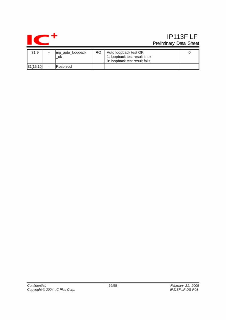
IP113F LFPreliminary Data Sheet
Confidential. 56/58 February 21, 2005Copyright © 2004, IC Plus Corp. IP113F LF-DS-R08
31.9 -- mg_auto_loopback _ok
RO Auto loopback test OK 1: loopback test result is ok 0: loopback test result fails
0
31[15:10] -- Reserved

IP113F LFPreliminary Data Sheet
Confidential. 57/58 February 21, 2005Copyright © 2004, IC Plus Corp. IP113F LF-DS-R08
4. Electrical Characteristics
4.1 Absolute Maximum Rating Stresses above those listed under Absolute Maximum Ratings may cause permanent damage to the device. Functional performance and device reliability are not guaranteed under these conditions. All voltages are specified with respect to GND. Supply Voltage –0.3V to Vcc+0.3V Input Voltage –0.3V to Vcc+0.3V Output Voltage –0.3V to Vcc+0.3V Storage Temperature -55°C to 125°C Ambient Operating Temperature (Ta) 0°C to 70°C 4.2. DC Characteristic Operating Conditions
Parameter Sym. Min. Typ. Max. Unit Conditions Supply Voltage VCC 2.375 2.5 2.645 V Power Consumption 0.475 W VCC=2.5v
Input Clock
Parameter Sym. Min. Typ. Max. Unit Conditions Frequency 25 MHz Frequency Tolerance -100 +100 PPM
I/O Electrical Characteristics
Parameter Sym. Min. Typ. Max. Unit Conditions Input Low Voltage VIL 0.8 V Input High Voltage VIH 2.0 V Output Low Voltage VOL 0.4 V IOH=4mA Output High Voltage VOH VCC_I
O-0.4 V IOL=4mA
5. Order Information
Part No. Package Notice IP113F 48-PIN LQFP -
IP113F LF 48-PIN LQFP Lead free

IP113F LFPreliminary Data Sheet
Confidential. 58/58 February 21, 2005Copyright © 2004, IC Plus Corp. IP113F LF-DS-R08
6. Package Detail
FSEATINGPLANE
1
12
13 24
25
36
3748
HE
PH
E
12"
12" cbeD F y
1
12
13 24
25
36
3748
2
2
AA2A
1
LL1
0.25
4
GAUGE PLANE
DETAIL "E"
D
"E"
θ
mm inch
AA1
1.600MAX.
A20.050~0.150
0.0630MAX.
b1.400 0.05
0.0020~0.0059
c0.200TYP
0.0551 0.0020
D0.127TYP
0.0078TYP
Ee
Hd0.500TYP
0.0050TYP
unitSymbol
yL1L
He
0"~7"0.100MAX.1.000REF
0.600 0.150
0"~7"0.0039MAX.0.0393REF
0.0236 0.006
0.0196TYP
+- +-
0.2756 0.0039+-7.000 0.100+-7.000 0.100+- 0.2756 0.0039+-
+- +-
9.000 0.250 0.3543 0.0098+- +-9.000 0.250 0.3543 0.0098+- +-
Notes:1. DIMENSION D & E DO NOT INCLUDE MOLD FLASH OR PROTRUSION.2. DIMENSION b DOES NOT INCLUDE DAMBAR PROTRUSION / INTRUSION.3. MAX. END FLASH IS 0.15MM.4. MAX. DAMBAR PROTRUSION IS 0.13MM.GENERAL APPEARANCE SPEC SHOULD BE BASED ON FINAL VISUAL INSPECTION SPEC.
ACTION DYNAMIC TECH(HK) TRADING COMPANYadd:Room1139-1142,Guoli Building,ZhenzhongRoad,Futian District,Shenzhen,ChinaTel:86-755-82539044 82539193Faxÿ86-755-82539160E-mail:[email protected]