manual de service bt2909sm (29m63) - bgh direct · 2011-10-11 · manual de service bt2909sm...
TRANSCRIPT
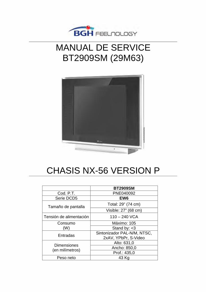
MANUAL DE SERVICEBT2909SM (29M63)
CHASIS NX-56 VERSION P
BT2909SMCod. P.T. PNE040092
Serie DCD5 EW6
Total: 29” (74 cm)Tamaño de pantalla
Visible: 27” (68 cm)
Tensión de alimentación 110 – 240 VCA
Máximo: 105Consumo(W) Stand by: <3
EntradasSintonizador PAL-N/M, NTSC,
2xAV, YPbPr, S-VideoAlto: 631,0
Ancho: 850,0Dimensiones
(en milímetros)Prof.: 435,0
Peso neto 43 Kg
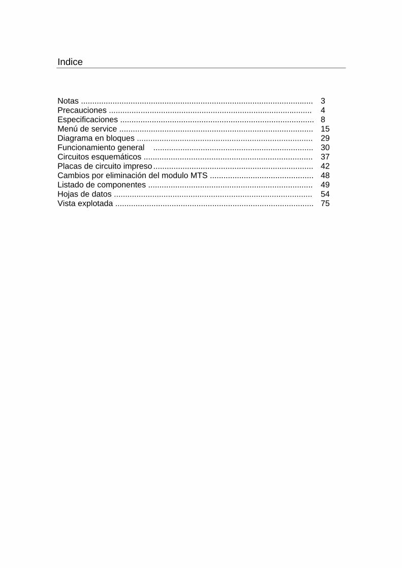
Indice
Notas ....................................................................................................... 3Precauciones .......................................................................................... 4Especificaciones ...................................................................................... 8Menú de service ...................................................................................... 15Diagrama en bloques .............................................................................. 29Funcionamiento general ....................................................................... 30Circuitos esquemáticos ........................................................................... 37Placas de circuito impreso ....................................................................... 42Cambios por eliminación del modulo MTS .............................................. 48Listado de componentes ......................................................................... 49Hojas de datos ........................................................................................ 54Vista explotada ........................................................................................ 75

Notas
Antes de salir del menu de service, se debe llevar el valor FACTORY HOTKEY, del menu 4, a 0. Despues de esto se debe apagar el televisor, volver a encenderlo y presionar el boton Menu para verificar que se accede al menu de usuario.
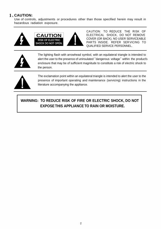
WARNING: TO REDUCE RISK OF FIRE OR ELECTRIC SHOCK, DO NOT
EXPOSE THIS APPLIANCE TO RAIN OR MOISTURE.
CAUTION: TO REDUCE THE RISK OFELECTRICAL SHOCK, DO NOT REMOVECOVER (OR BACK). NO USER SERVICEABLEPARTS INSIDE. REFER SER VICING TOQUALIFIED SERVICE PERSONNEL.
The lighting flash with arrowhead symbol, with an equilateral triangle is intended to
alert the user to the presence of uninsulated voltage within the products
enclosure that may be of sufficient magnitude to constitute a risk of electric shock to
the person.
The exclamation point within an equilateral triangle is intended to alert the user to the
presence of important operating and maintenance (servicing) instructions in the
literature accompanying the appliance.
CAUTION:Use of controls, adjustments or procedures other than those specified herein may result inhazardous radiation exposure.
CAUTIONRISK RISK OF OF ELECTRIELECTRICC
SHOCK SHOCK DO DO NOT NOT OPEN.OPEN.
2
dangerous
1、

3
FOR YOUR PERSONAL SAFETY1. When the power cord or plug is damaged or frayed, unplug this television set from the wall outlet and refer servicing to
qualified service personnel.
2. Do not overload wall outlets and extension cords as this can result in fire or electric shock.
3. Do not allow anything to rest on or roll over the power cord, and do not place the TV where power cord is subject totraffic or abuse. This may result in a shock or fire hazard.
4. Do not attempt to service this television set yourself as opening or removing covers may expose you to dangerousvoltage or other hazards. Refer all servicing to qualified service personnel.
5. Never push objects of any kind into this television set through cabinet slots as they may touch dangerous voltagepoints or short out parts that could result in a fire or electric shock. Never spill liquid of any kind on the television set.
6. If the television set has been dropped or the cabinet has been damaged, unplug this television set from the wall outletand refer servicing to qualified service personnel.
7. If liquid has been spilled into the television set, unplug this television set from the wall outlet and refer servicing toqualified service personnel.
8. Do not subject your television set to impact of any kind. Be particularly careful not to damage the picture tube surface.
9. Unplug this television set from the wall outlet before cleaning. Do not use liquid cleaners or aerosol cleaners. Use adamp cloth for cleaning.
10.1. Do not place this television set on an unstable cart, stand, or table. The television set may fall, causing serious injuryto a child or an adult, and serious damage to the appliance. Use only with a cart or stand recommended by themanufacturer, or sold with the television set. Wall or shelf mounting should follow the manufacturer s instructions, andshould use a mounting kit approved by the manufacturer.
10.2. An appliance and cart combination should be moved with care. Quick stops, excessive force, and uneven surfacesmay cause the appliance and cart combination to overturn.
CAUTION:
Read all of these instructions. Save these instructions for later use. Follow all Warnings andInstructions marked on the audio equipment.
1. Read Instructions- All the safety and operating instructions should be read before the product is operated.
2. Retain Instructions- The safety and operating instructions should be retained for future reference.
3. Heed Warnings- All warnings on the product and in the operating instructions should be adhered to.
4. Follow Instructions- All operating and use instructions should be followed.
IMPORTANT SAFETY INSTRUCTIONS

4
PROTECTION AND LOCATION OF YOUR SET11. Do not use this television set near water ... for example, near a bathtub, washbowl, kitchen sink, or laundry tub, in a
wet basement, or near a swimming pool, etc.Never expose the set to rain or water. If the set has been exposed to rain or water, unplug the set from the walloutlet and refer servicing to qualified service personnel.
12. Choose a place where light (artificial or sunlight) does not shine directly on the screen.
13. Avoid dusty places, since piling up of dust inside TV chassis may cause failure of the set when high humidity persists.
14. The set has slots, or openings in the cabinet for ventilation purposes, to provide reliable operation of the receiver, toprotect it from overheating. These openings must not be blocked or covered.
Never cover the slots or openings with cloth or other material.Never block the bottom ventilation slots of the set by placing it on a bed, sofa, rug, etc.Never place the set near or over a radiator or heat register.Never place the set in enclosure, unless proper ventilation is provided.
PROTECTION AND LOCATION OF YOUR SET15.1. If an outside antenna is connected to the television set, be sure the antenna system is grounded so as to provide some
protection against voltage surges and built up static charges, Section 810 of the National Electrical Code, NFPA No.70-1975, provides information with respect to proper grounding of the mast and supporting structure, grounding of thelead-in wire to an antenna discharge unit, size of grounding conductors, location of antenna discharge unit, connectionto grounding electrode, and requirements for the grounding electrode.
15.2. Note to CATV system installer : (Only for the television set with CATV reception)
This reminder is provided to call the CATV system attention to Article 820-40 of the NEC that providesguidelines for proper grounding and, in particular, specifies that the cable ground shall be connected to the groundingsystem of the building, as close to the point of cable entry as practical.
16. An outside antenna system should not be located in the vicinity of overhead power lines or other electric lights or powercircuits, or where it can fall into such power lines or circuits. When installing an outside antenna system, extreme careshould be taken to keep from touching such power lines or circuits as contact with them might be fatal.
17. For added protection for this television set during a lightning storm, or when it is left unattended and unused for longperiods of time, unplug it from the wall outlet and disconnect the antenna. This will prevent damage due to lightningand power-line surges.
ANTENNALEAD- IN WIRE
ANTENNA DISCHARGEUNIT (NEC SECTION810-20)
GROUNDINGCONDUCTORS(NEC SECTION810-21)
GROUND CLAMPS
POWER SERVICE GROUNDINGELECTRODE SYSTEM(NEC ART 250. PART H)
ELECTRIC SERVICEEQUIPMENT
GROUND CLAMP
NEC-NATIONAL ELECTRICAL CODE
EXAMPLE OF ANTENNA GROUNDING AS PER
NATIONAL ELECTRICAL CODE
EXAMPLE OF ANTENNA GROUNDING AS PER NATIONAL ELECTRICAL CODE INSTRUCTIONS
a built-in
installer s
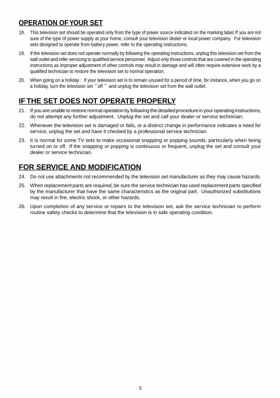
OPERATION OF YOUR SET18. This television set should be operated only from the type of power source indicated on the marking label. If you are not
sure of the type of power supply at your home, consult your television dealer or local power company. For televisionsets designed to operate from battery power, refer to the operating instructions.
19. If the television set does not operate normally by following the operating instructions, unplug this television set from thewall outlet and refer servicing to qualified service personnel. Adjust only those controls that are covered in the operatinginstructions as improper adjustment of other controls may result in damage and will often require extensive work by aqualified technician to restore the television set to normal operation.
20. When going on a holiday : If your television set is to remain unused for a period of time, for instance, when you go ona holiday, turn the television set and unplug the television set from the wall outlet.
IF THE SET DOES NOT OPERATE PROPERLY21. If you are unable to restore normal operation by following the detailed procedure in your operating instructions,
do not attempt any further adjustment. Unplug the set and call your dealer or service technician.
22. Whenever the television set is damaged or fails, or a distinct change in performance indicates a need forservice, unplug the set and have it checked by a professional service technician.
23. It is normal for some TV sets to make occasional snapping or popping sounds, particularly when beingturned on or off. If the snapping or popping is continuous or frequent, unplug the set and consult yourdealer or service technician.
FOR SERVICE AND MODIFICATION24. Do not use attachments not recommended by the television set manufacturer as they may cause hazards.
25. When replacement parts are required, be sure the service technician has used replacement parts specifiedby the manufacturer that have the same characteristics as the original part. Unauthorized substitutionsmay result in fire, electric shock, or other hazards.
26. Upon completion of any service or repairs to the television set, ask the service technician to performroutine safety checks to determine that the television is in safe operating condition.
5
off

Model
Item
Master Data
-Version 1 1-Customer ID EM EM-Destination EM EM-Brand
-BOM NO. 03-B185SAE-SC31 03-DM63SAE-SC31S-Chassis
Reception
-Tuning [Channels Amt.] 181 181-Tuning [Technology] PLL PLL-Tuning [Indication] Channel Channel-Frequency Bands Antenna AND Cable Antenna AND Cable-IF Frequency 45.7MHz 45.7MHz-TV Systems (Color+ Sound) PAL M/N NTSC M PAL M/N NTSC M-AV Systems NTSC PAL NTSC PALPicture-Processing
-SCAN Standard Standard-Wide Screen Switching
-Comb filter
-Picture Enhancement
LTI / CTI
Black Stretch
Dynamic Skin
Others
-Picture Control [General]
Brightness X X Sharpness X X Contrast X X Tint X X Color X X-Picture Control [Special]
Smart Pictures * modes 4 modes 4 modes VM
Color Temperature 3 modes 3 modes Others
-Picture Noise Reduction X XPicture – Display
-CRT Type
Normal Flat
Pure Flat X X Super Flat
-Deflection system
1Fh X X 2Fh
-Tube Technology
Iron
AK X X Black Matrix
Others
-CRT Deflection ( * Deg.) 110 120-CRT Magnetic Field
-Screen Type 4:3 4:3-Screen Size / Vis. Size 29' 21' Super SlimSound
-Audio Power Consumption 5W+5W 4W+4W-Surround Sound
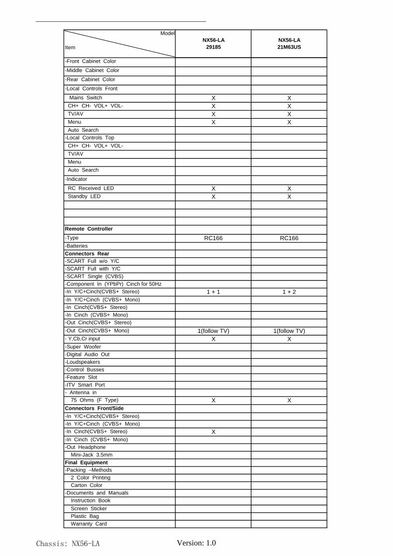
NX56-LA29185
NX56-LA21M63US
Chassis: NX56-LA Version: 1.0

Model
ItemNX56-LA
29185NX56-LA21M63US
-Nicam
-America Stereo (MTS,BTSC,MPS) X X-America SAP
-Korea Stereo
-Thai Bilingual
-Super Woofer
-AVL
-Sound Control [General]
Volume X X Mute X X -Sound Control [Special]
Treble
Bass
Balance X X Equalizer
Smart Sound * modes
Others
-Speakers Quantity 2X1 2X1User Interface
-Menu Language English/Portugal/Espanol English/Portugal/Espanol -Features [General]
AT
Biological Clock
Calendar
Clock
Channel Swap X X Channel Naming
Child Lock X X Favorite Channel X X Game
Hotel Mode X X High Sensitive
Notebook
On/Off Timer
Preset X X Recall X X Rotation
Sleep X X AVC
-Features [Special]
V-chip / CCD X X Teletext *Pages
Others
New Features
Smart signal
Voltage display
环境光检测
Easy search
Tuning Features
-Auto Channel Program X X-Auto/Manual Tuning X X-Auto/Manual Store X X-Fine Tuning X X-Factory Mode X X-Service Mode
Cabinet
-Cabinet Name
Chassis: NX56-LA Version: 1.0
Model
ItemNX56-LA
29185NX56-LA21M63US
-Front Cabinet Color
-Middle Cabinet Color
-Rear Cabinet Color
-Local Controls Front
Mains Switch X X CH+ CH- VOL+ VOL- X X TV/AV X X Menu X X Auto Search
-Local Controls Top
CH+ CH- VOL+ VOL-
TV/AV
Menu
Auto Search
-Indicator
RC Received LED X X Standby LED X X
Remote Controller
-Type RC166 RC166-Batteries
Connectors Rear
-SCART Full w/o Y/C
-SCART Full with Y/C
-SCART Single (CVBS)
-Component In (YPbPr) Cinch for 50Hz
-In Y/C+Cinch(CVBS+ Stereo) 1 + 1 1 + 2-In Y/C+Cinch (CVBS+ Mono)
-In Cinch(CVBS+ Stereo)
-In Cinch (CVBS+ Mono)
-Out Cinch(CVBS+ Stereo)
-Out Cinch(CVBS+ Mono) 1(follow TV) 1(follow TV)- Y,Cb,Cr input X X-Super Woofer
-Digital Audio Out
-Loudspeakers
-Control Busses
-Feature Slot
-ITV Smart Port
- Antenna in
75 Ohms (F Type) X XConnectors Front/Side
-In Y/C+Cinch(CVBS+ Stereo)
-In Y/C+Cinch (CVBS+ Mono)
-In Cinch(CVBS+ Stereo) X-In Cinch (CVBS+ Mono)
-Out Headphone
Mini-Jack 3.5mm
Final Equipment
-Packing –Methods
2 Color Printing
Carton Color
-Documents and Manuals
Instruction Book
Screen Sticker
Plastic Bag
Warranty Card
Chassis: NX56-LA Version: 1.0
Model
ItemNX56-LA
29185NX56-LA21M63US
Guarantee Doc.
Warning Label
Approbation Label
Others
-Languages DFU
-Indication on BACKOVER
Made-in in family sheet
FCC/Elect Shock Caution Label
CE/Elect Shock Caution Label
Warning Label
Others
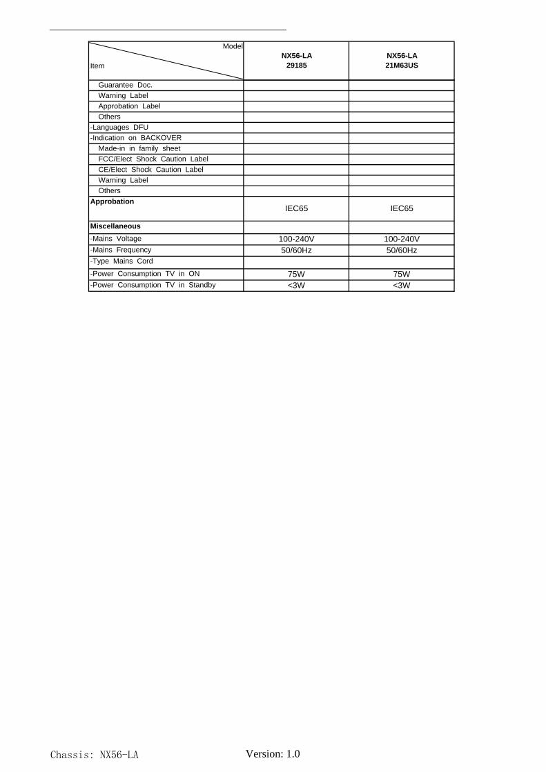
Miscellaneous
-Mains Voltage 100-240V 100-240V-Mains Frequency 50/60Hz 50/60Hz-Type Mains Cord
-Power Consumption TV in ON 75W 75W-Power Consumption TV in Standby <3W <3W
ApprobationIEC65 IEC65
Chassis: NX56-LA Version: 1.0

Chassis Name NX56-AP&NX56B-AP Serial No.
Issued on 2008-01-18 Page Page 1 of 17
Updated on 2009-04-24 Version 4.0
NX56-AP&NX56B-AP Chassis Alignment Procedure
Disclosure Proprietary Information: These drawings and specifications are the

Chassis Name NX56-AP&NX56B-AP Serial No.
Issued on 2008-01-18 Page Page 2 of 17
Updated on 2009-04-24 Version 4.0
copied or used as the basis for the manufacture or sale of apparatus or
Version Information: Version states by two Arabic Numbers, which is
separated by one dot, e.g. 1.2. The first number “1” means the version of approved file, the second one ”2” means the version of draft.

Chassis Name NX56-AP&NX56B-AP Serial No.
Issued on 2008-01-18 Page Page 3 of 17
Updated on 2009-04-24 Version 4.0
Revision History Model No. Status Date Comment
Prepared by Luo MJ 2008-01-18
Checked by 29A41/NX56
Released by
Ver0.1
03-BA41UAE-TH32(29A41/NX56)
Prepared by Luo MJ 2008-01-18
Checked by Guo Guangyuan 2008-01-23 All NX56-AP
chassis
Released by Zhou Songming 2008-01-23
Ver1.0
1. Updated the B+ specs accord
with 21” tube.
2. Updated the description accord
with the software changing.
Prepared by Luo MJ 2008-07-04
Checked by Guo Guangyuan 2008-07-04 All NX56-AP
chassis
Released by Zhou Songming 2008-07-04
Ver2.0
1. Updated the B+ specs accord
with 25” tube.
2. Updated the description accord
with the software changing.
Prepared by GUO HQ 2009-02-09
Checked by
14F1
21NCM86
29E64S Released by Zhou Songming 2009-02-09
Ver3.0
Prepared by Luo MJ 2009-04-24
Checked by All NX56-AP&
NX56B-AP chassis Released by
Ver4.0
1. Updated the description accord
with the software changing.
2. Updated the chassis name.
Prepared by
Checked by
Released by
Prepared by
Checked by
Released by
Chassis Name NX56-AP&NX56B-AP Serial No.
Issued on 2008-01-18 Page Page 4 of 17
Updated on 2009-04-24 Version 4.0
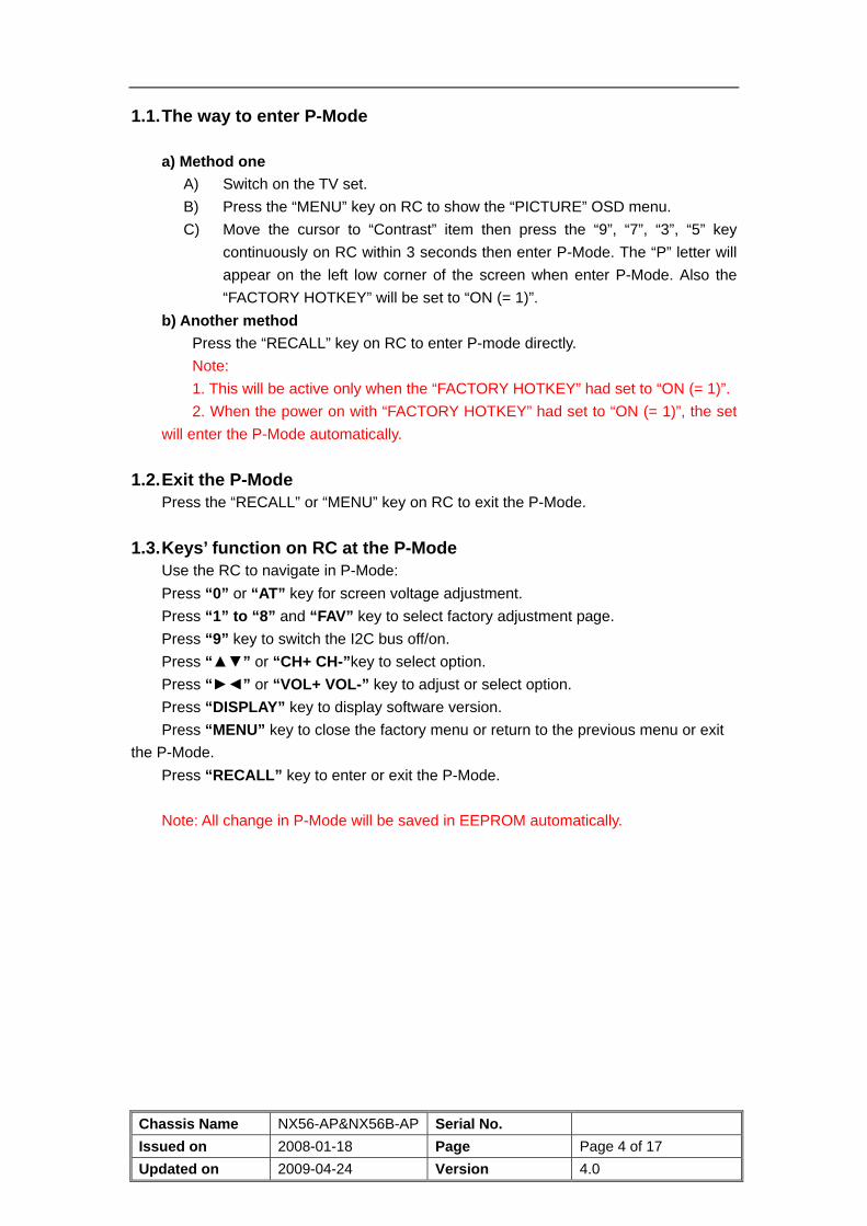
1.1. The way to enter P-Mode a) Method one
A) Switch on the TV set.
B) Press the “MENU” key on RC to show the “PICTURE” OSD menu.
C) Move the cursor to “Contrast” item then press the “9”, “7”, “3”, “5” key
continuously on RC within 3 seconds then enter P-Mode. The “P” letter will
appear on the left low corner of the screen when enter P-Mode. Also the
“FACTORY HOTKEY” will be set to “ON (= 1)”.
b) Another method
Press the “RECALL” key on RC to enter P-mode directly.
Note:
1. This will be active only when the “FACTORY HOTKEY” had set to “ON (= 1)”.
2. When the power on with “FACTORY HOTKEY” had set to “ON (= 1)”, the set
will enter the P-Mode automatically.
1.2. Exit the P-Mode Press the “RECALL” or “MENU” key on RC to exit the P-Mode.
1.3. Keys’ function on RC at the P-Mode Use the RC to navigate in P-Mode:
Press “0” or “AT” key for screen voltage adjustment.
Press “1” to “8” and “FAV” key to select factory adjustment page.
Press “9” key to switch the I2C bus off/on.
Press “▲▼” or “CH+ CH-”key to select option.
Press “►◄” or “VOL+ VOL-” key to adjust or select option.
Press “DISPLAY” key to display software version.
Press “MENU” key to close the factory menu or return to the previous menu or exit
the P-Mode.
Press “RECALL” key to enter or exit the P-Mode.
Note: All change in P-Mode will be saved in EEPROM automatically.

Chassis Name NX56-AP&NX56B-AP Serial No.
Issued on 2008-01-18 Page Page 5 of 17
Updated on 2009-04-24 Version 4.0
1.4. The adjustment page list an RC key function on P-Mode: RC key Item Description
0 Screen voltage adjustment Adjust the VG2 voltage
1 Vertical geometry Vertical geometry page
2 Horizontal geometry Horizontal geometry page
3 White Balance Adjustment White Balance page
4 Setup and option page 4
5 Setup and option page 5
6 Setup and option page 6
7 Setup and option page 7
8 Setup and option page 8
FAV
Setup and option page select
Setup and option page 9
9 I2C Bus OFF/ON Press this key to enter or exit BUS OFF mode
DISPLAY Software version Display software version
MENU Close menu or exit the P-Mode Close the factory menu or return to the previous
menu or exit the P-Mode
RECALL P-Mode hotkey Enter or exit the P-Mode
AT Screen voltage adjustment with AKB Adjust the VG2 voltage
Chassis Name NX56-AP&NX56B-AP Serial No.
Issued on 2008-01-18 Page Page 6 of 17
Updated on 2009-04-24 Version 4.0
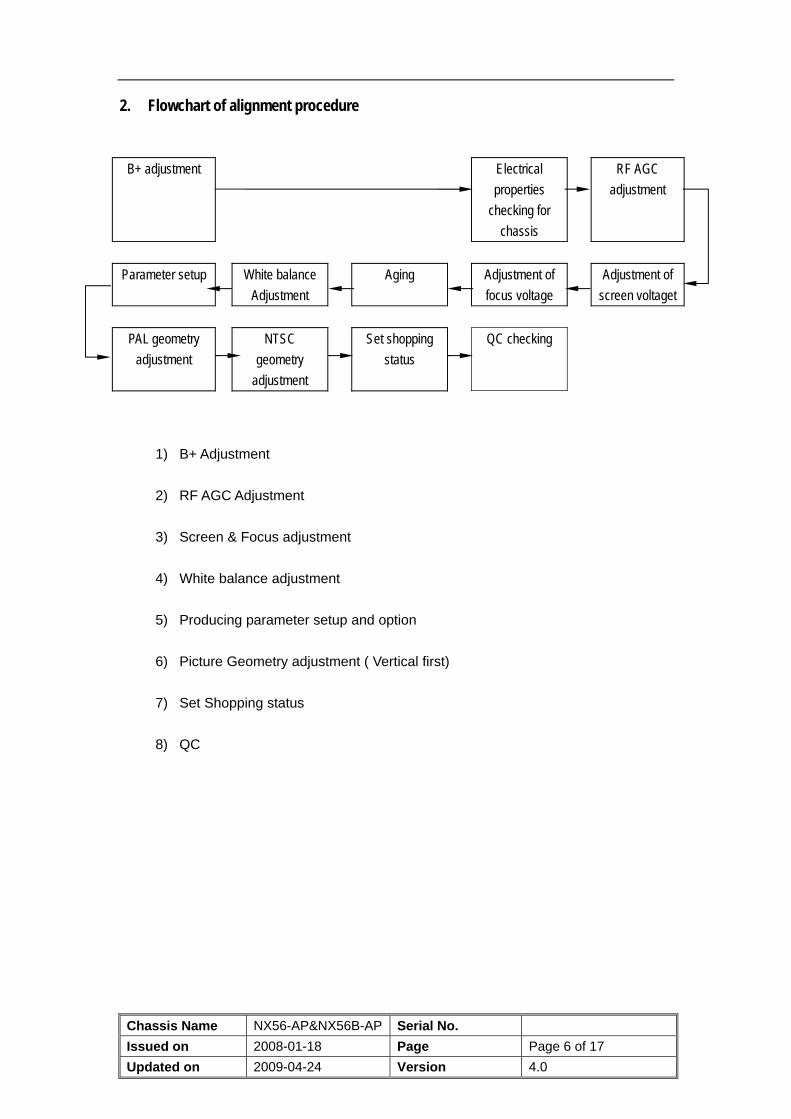
2. Flowchart of alignment procedure
B+ adjustment Electrical
properties checking for
chassis
RF AGC adjustment
Parameter setup White balance
Adjustment Aging Adjustment of
focus voltage Adjustment of
screen voltaget
PAL geometry
adjustment NTSC
geometry adjustment
Set shopping status
QC checking
1) B+ Adjustment
2) RF AGC Adjustment
3) Screen & Focus adjustment
4) White balance adjustment
5) Producing parameter setup and option
6) Picture Geometry adjustment ( Vertical first)
7) Set Shopping status
8) QC
Chassis Name NX56-AP&NX56B-AP Serial No.
Issued on 2008-01-18 Page Page 7 of 17
Updated on 2009-04-24 Version 4.0
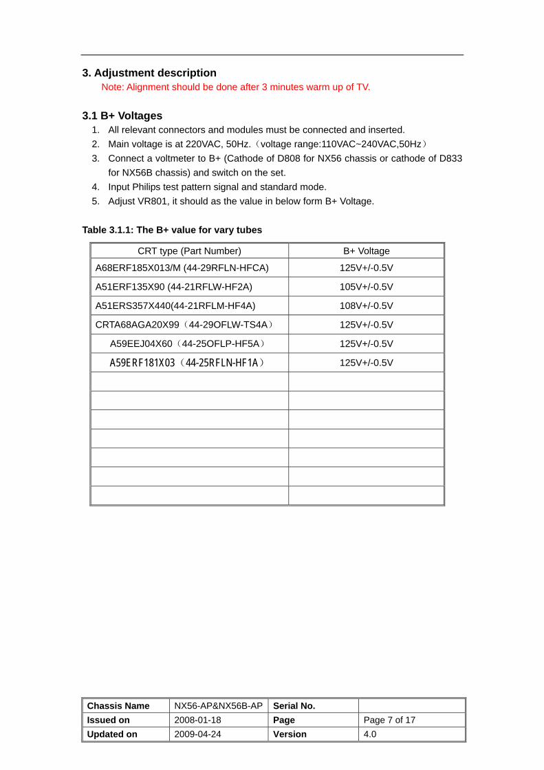
3. Adjustment description Note: Alignment should be done after 3 minutes warm up of TV.
3.1 B+ Voltages 1. All relevant connectors and modules must be connected and inserted.
2. Main voltage is at 220VAC, 50Hz.(voltage range:110VAC~240VAC,50Hz)
3. Connect a voltmeter to B+ (Cathode of D808 for NX56 chassis or cathode of D833
for NX56B chassis) and switch on the set.
4. Input Philips test pattern signal and standard mode.
5. Adjust VR801, it should as the value in below form B+ Voltage.
Table 3.1.1: The B+ value for vary tubes
CRT type (Part Number) B+ Voltage
A68ERF185X013/M (44-29RFLN-HFCA) 125V+/-0.5V
A51ERF135X90 (44-21RFLW-HF2A) 105V+/-0.5V
A51ERS357X440(44-21RFLM-HF4A) 108V+/-0.5V
CRTA68AGA20X99(44-29OFLW-TS4A) 125V+/-0.5V
A59EEJ04X60(44-25OFLP-HF5A) 125V+/-0.5V
A59ERF181X03(44-25RFLN-HF1A) 125V+/-0.5V
Chassis Name NX56-AP&NX56B-AP Serial No.
Issued on 2008-01-18 Page Page 8 of 17
Updated on 2009-04-24 Version 4.0
3.2 RF AGC alignment 3.2.1 Method 1
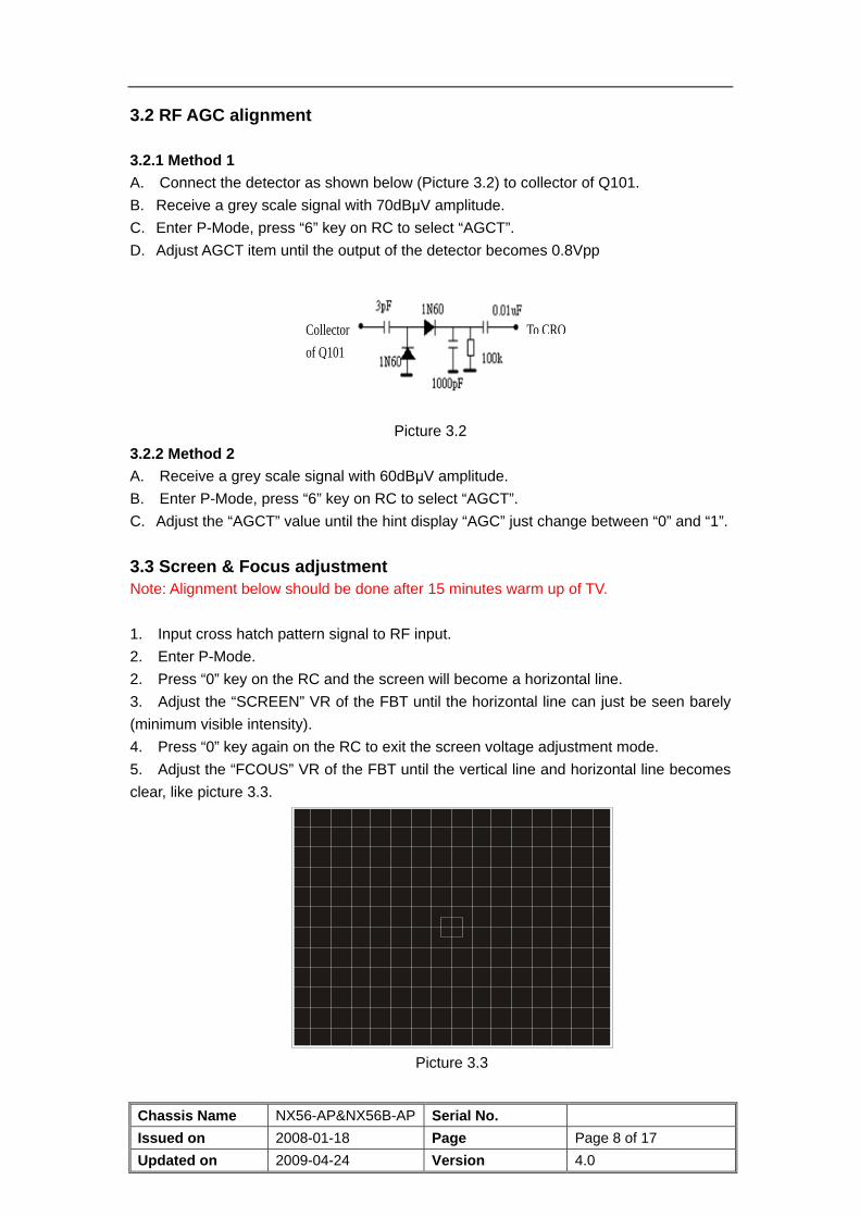
A. Connect the detector as shown below (Picture 3.2) to collector of Q101.
B. Receive a grey scale signal with 70dBμV amplitude.
C. Enter P-Mode, press “6” key on RC to select “AGCT”.
D. Adjust AGCT item until the output of the detector becomes 0.8Vpp
Picture 3.2
3.2.2 Method 2
A. Receive a grey scale signal with 60dBμV amplitude.
B. Enter P-Mode, press “6” key on RC to select “AGCT”.
C. Adjust the “AGCT” value until the hint display “AGC” just change between “0” and “1”.
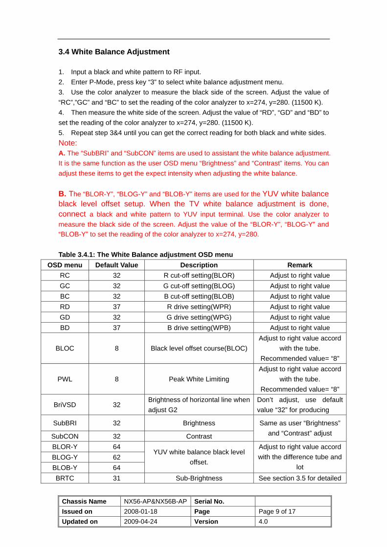
3.3 Screen & Focus adjustment Note: Alignment below should be done after 15 minutes warm up of TV.
1. Input cross hatch pattern signal to RF input.
2. Enter P-Mode.
2. Press “0” key on the RC and the screen will become a horizontal line.
3. Adjust the “SCREEN” VR of the FBT until the horizontal line can just be seen barely
(minimum visible intensity).
4. Press “0” key again on the RC to exit the screen voltage adjustment mode.
5. Adjust the “FCOUS” VR of the FBT until the vertical line and horizontal line becomes
clear, like picture 3.3.
Picture 3.3
Collector of Q101
To CRO
Chassis Name NX56-AP&NX56B-AP Serial No.
Issued on 2008-01-18 Page Page 9 of 17
Updated on 2009-04-24 Version 4.0
3.4 White Balance Adjustment 1. Input a black and white pattern to RF input.
2. Enter P-Mode, press key “3” to select white balance adjustment menu.
3. Use the color analyzer to measure the black side of the screen. Adjust the value of
“RC”,”GC” and “BC” to set the reading of the color analyzer to x=274, y=280. (11500 K).
4. Then measure the white side of the screen. Adjust the value of “RD”, “GD” and “BD” to
set the reading of the color analyzer to x=274, y=280. (11500 K).
5. Repeat step 3&4 until you can get the correct reading for both black and white sides.
Note: A. The “SubBRI” and “SubCON” items are used to assistant the white balance adjustment.
It is the same function as the user OSD menu “Brightness” and “Contrast” items. You can
adjust these items to get the expect intensity when adjusting the white balance.
B. The “BLOR-Y”, “BLOG-Y” and “BLOB-Y” items are used for the YUV white balance black level offset setup. When the TV white balance adjustment is done, connect a black and white pattern to YUV input terminal. Use the color analyzer to
measure the black side of the screen. Adjust the value of the “BLOR-Y”, “BLOG-Y” and
“BLOB-Y” to set the reading of the color analyzer to x=274, y=280.
Table 3.4.1: The White Balance adjustment OSD menu
OSD menu Default Value Description Remark
RC 32 R cut-off setting(BLOR) Adjust to right value
GC 32 G cut-off setting(BLOG) Adjust to right value
BC 32 B cut-off setting(BLOB) Adjust to right value
RD 37 R drive setting(WPR) Adjust to right value
GD 32 G drive setting(WPG) Adjust to right value
BD 37 B drive setting(WPB) Adjust to right value
BLOC 8 Black level offset course(BLOC)
Adjust to right value accord
with the tube.
Recommended value= “8”
PWL 8 Peak White Limiting
Adjust to right value accord
with the tube.
Recommended value= “8”
BriVSD 32 Brightness of horizontal line when
adjust G2
Don’t adjust, use default
value “32” for producing
SubBRI 32 Brightness
SubCON 32 Contrast
Same as user “Brightness”
and “Contrast” adjust
BLOR-Y 64
BLOG-Y 62
BLOB-Y 64
YUV white balance black level
offset.
Adjust to right value accord
with the difference tube and
lot
BRTC 31 Sub-Brightness See section 3.5 for detailed

Chassis Name NX56-AP&NX56B-AP Serial No.
Issued on 2008-01-18 Page Page 10 of 17
Updated on 2009-04-24 Version 4.0
3.5 Sub brightness adjustment 1. Input eight steps gray signal.
2. Press key “3” to enter sub-brightness adjustment.
3. At dynamic state, adjust “BRTC” until the secondary gray bar just to be seen. (like
picture 3.5.)
The 2nd gray scale
Picture 3.5
3.6 Picture Geometry adjustment
3.6.1 Vertical geometry adjustment
1. Input a PAL crosshatch pattern signal to RF input.
2. Enter P-Mode, press key “1” to select vertical geometry adjustment. (The OSD menu
for this adjustment as below table 3.6.1. For NTSC signal, the “-50” will be replaced with
“-60”.)
3. Adjust the value of the corresponding item to make the vertical geometry of the
pattern look good.
4. Apply NTSC signal to adjust these value for NTSC vertical geometry.
Table 3.6.1: The vertical geometry adjustment OSD menu
OSD menu Default Value Description Remark
VSLOPE-50 32 Vertical slope(VS) Adjust to right value
VCEN-50 32 Vertical shift (VSH) Adjust to right value
VSIZE-50 32 Vertical amplitude(VA) Adjust to right value
VZOOM-50 25 Vertical zoom(VX) Adjust to right value
VSC-50 32 S-correction(SC) Adjust to right value
VSCROLL-50 32 Vertical Scroll(VCS) Adjust to right value
Note:
1. For NTSC signal, the “-50” will be replaced with “-60”.
2. For NTSC signal, only the “VCEN-60” and “VSIZE-60” items need the adjustment,
the other items use the same data as PAL signal.

Chassis Name NX56-AP&NX56B-AP Serial No.
Issued on 2008-01-18 Page Page 11 of 17
Updated on 2009-04-24 Version 4.0
3. On producing, please use the “AUTO OFFSET” (On page “2”) function to easy the
geometry adjustment of NTSC signal. When finished the PAL signal geometry adjustment,
press “2” key to enter page “2” to select “AUTO OFFSET” item, press “►” key to active the
automatic offset function. Then the geometry adjustment of NTSC signal will finish
automated. If the geometry of NTSC signal is look good, you don’t need to adjust the
geometry of NTSC signal any more.
3.6.2 Horizontal geometry adjustment
1. Input a PAL crosshatch pattern signal to RF input.
2. Enter P-Mode, press key “2” to select horizontal geometry adjustment. (The OSD
menu for this adjustment as below table 3.6.2. For NTSC signal, the “-50” will be replaced
with “-60”.)
3. Adjust the value of the corresponding item to make the horizontal geometry of the
pattern look good.
4. Apply NTSC signal to adjust these value for NTSC horizontal geometry.
Table 3.6.2: The horizontal geometry adjustment OSD menu
OSD menu Default Value Description Remark
HCEN-50 32 Horizontal shift(HSH) Adjust to right value
HSIZE-50 32 EW width(EWW) Adjust to right value
HPARA-50 32 EW parabola width(PW) Adjust to right value
HTRAP-50 32 EW trapezium(TC) Adjust to right value
HCNRT-50 32 EW upper corner parabola(UCP) Adjust to right value
HCNRB-50 32 EW lower corner parabola(LCP) Adjust to right value
HBOW-50 32 Horizontal bow(HB) Adjust to right value
HPARALLEL 32 Horizontal parallelogram(HP) Adjust to right value
AUTO OFFSET 0 Automatic offset NTSC geometry See below description
for detailed
Note:
1. For NTSC signal, the “-50” will be replaced with “-60”.
2. For NTSC signal, only the “HCEN-60” and “HSIZE-60” items need the adjustment,
the other items use the same data as PAL signal.
3. On producing, please use the “AUTO OFFSET” (On page “2”) function to easy the
geometry adjustment of NTSC signal. When finished the PAL signal geometry adjustment,
press “2” key to enter page “2” to select “AUTO OFFSET” item, press “►” key to active the
automatic offset function. Then the geometry adjustment of NTSC signal will finish
automated. If now the geometry of NTSC signal is look good, it not needed to adjust the
geometry of NTSC signal any more.
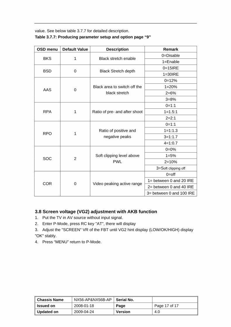
3.7 Producing parameter setup and option

Chassis Name NX56-AP&NX56B-AP Serial No.
Issued on 2008-01-18 Page Page 12 of 17
Updated on 2009-04-24 Version 4.0
1. Enter P-Mode, press key “4” to select page “4”.Set the corresponding item to require
value. See below table 3.7.1 for detailed description.
Table 3.7.1: Producing parameter setup and option page “4”
OSD menu Default Value Description Remark
0=Aging mode off WARM UP STATUS 0 Set aging mode
1=Aging mode on
SHOP INIT 0 Set the shopping status 0=>1= Set the shopping status
DCXO 2 Crystal oscillator
frequency adjustment
Adjust this value to get the max
color synchronization range.
Don’t adjust, use default value for
producing
0=”FACTORY HOTKEY” off FACTORY HOTKEY 1 Set factory hotkey
1=”FACTORY HOTKEY” on
ON=On when power on
STB=Standby when power on POWER ON MODE LAST Set the power on mode
LAST=Last power off status
EEPROM INIT 0 EEPROM initial 0=>1=Active EEPROM initial
POWER LOW 101 Recommended value= “16”
POWER HIGH 176
Set the “Voltage display”
“LOW” and “HIGH”
threshold Recommended value= “168”
DEFAULT SND. SYS DK Set the default sound
system when auto store
Set the right value according to the
sales area
0= Blue background for TV and AV
while no signal
1=Black background for TV and AV
while no signal BLUE BACK OPT 2 Set the Background
option while no signal 2=Snowy background for TV and
black background for AV while no
signal
BLACK BRI 40
Set the black
background brightness
while no signal
Recommended value= “20”
BRI CURVE >> Set the brightness curve
CON CURVE >> Set the contrast curve
COL CURVE >> Set the colour curve
VOL CURVE >> Set the volume curve
Press “►◄” or “VOL+ VOL-” key
to enter a sub-menu to do the
setup, and press “MENU” key the
previous menu
Description:
1). Set the shopping status
When trigger the “SHOP INIT” item form “0” to “1”, the TV will be put on selling status.
The TV status after shopping status:
A. “FACTORY HOTKEY” had set to “OFF”.

Chassis Name NX56-AP&NX56B-AP Serial No.
Issued on 2008-01-18 Page Page 13 of 17
Updated on 2009-04-24 Version 4.0
B. Picture set to “Standard” status. (Brightness=50, Contrast=50, Colour=50, White
tone=Normal.)
C. Sound set normal.(Volume=30,Balance=50.)
D.
2). Set the user picture and sound curve value
A. Brightness curve:
OSD menu Default Value Description Remark
BRI0 0 Set the minimal brightness when user Brightness=0 Set to 3
BRI50 32 Set the brightness when user Brightness=50
BRI100 63 Set the maximal brightness when user Brightness=0
Use default value
B. Contrast curve:
OSD menu Default Value Description Remark
CON0 0 Set the minimal contrast when user Contrast=0 Set to 3
CON50 32 Set the contrast when user Contrast=50
CON100 63 Set the maximal contrast when user Contrast=0
Use default value
C. Colour curve:
OSD menu Default Value Description Remark
COL0 0 Set the minimal colour when user Colour=0 Set to 3
COL50 32 Set the colour when user Color=50
COL100 63 Set the maximal colour when user Colour=0
Use default value
D. Volume curve:
OSD menu Default Value Description Remark
VOL0 0 Set the volume when user Volume=0
VOL10 38 Set the volume when user Volume=10
Use default value
VOL30 65 Set the volume when user Volume=30 Set to 63
VOL50 71 Set the volume when user Volume=50 Set to 69
VOL80 77 Set the volume when user Volume=80 Set to 75
VOL100 83 Set the volume when user Volume=100 Set to 81
3). Set the value for “POWER LOW” and “POWER HIGH”
A. Connect the main voltage at low threshold 95VAC/50Hz.
B. Select item “POWER LOW”.
C. Adjust the value until the hint display just change between “AC: NORMAL” and “AC:
LOW”.
D. Connect the main voltage at high threshold 255VAC/50Hz.
E. Select item “POWER HIGH.
F. Adjust the value until the hint display just change between “AC: NORMAL” and “AC:
HIGH”.

Chassis Name NX56-AP&NX56B-AP Serial No.
Issued on 2008-01-18 Page Page 14 of 17
Updated on 2009-04-24 Version 4.0
2. Enter P-Mode, press key “5” to select page “5”. Set the corresponding item to require
value. See below table 3.7.2 for detailed description.
Table 3.7.2: Producing parameter setup and option page “5”
OSD menu Default Value Description Remark
0=EHT tracking only on vertical Track. Mode 1 EHT tracking mode
1=EHT tracking on vertical and EW
VX Normal 25 4:3 mode vertical zoom Don’t adjust, use default
VX Compr. 0 16:9 mode vertical zoom Don’t adjust, use default
WBF 5 Wide blanking start Don’t adjust, use default
WBR 8 Wide blanking end Don’t adjust, use default
GET OFFSET 0 Get offset See below description for detailed
ColdRC 61 Recommended value= “61”
ColdGC 56
Cold color temperature R
and G cut-off offset Recommended value= “56”
ColdRD 61 Recommended value= “61”
ColdGD 66
Cold color temperature R
and G drive offset Recommended value= “66”
WarmRC 72 Recommended value= “72”
WarmGC 71
Warm temperature R and G
cut-off offset Recommended value= “71”
WarmRD 65 Recommended value= “65”
WarmGD 64
Warm color temperature R
and G drive offset Recommended value= “64”
Description for AUTO OFFSET and GET OFFSET:
The “GET OFFSET” can use to make the EEPROM copy by PE engineer. When the
PAL and NTSC geometry adjustment had finished, trigger the “GET OFFSET” from “0” to
“1” to store the geometry offset datum between PAL and NTSC in EEPROM.
On producing, these geometry offset datum can use to easy the NTSC geometry
adjustment. When finished the PAL geometry adjustment, trigger the “AUTO OFFSET”
from “0” to “1”, then the geometry adjustment of NTSC signal will finish automated. If now
the geometry of NTSC signal is look good, it not needed to adjust the geometry of NTSC
signal any more.
3. Enter P-Mode, press key “6” to select page “6”. Set the corresponding item to require
value. See below table 3.7.3 for detailed description.
Table 3.7.3: Producing parameter setup and option page “6”
OSD menu Default Value Description Remark
AGCT 32 AGC take over point
AGC 0 AGC take over point indicate
See section “3.2 RF AGC alignment”
for detailed.
OIF 32 IF demodulator offset Don’t adjust, use default
Chassis Name NX56-AP&NX56B-AP Serial No.
Issued on 2008-01-18 Page Page 15 of 17
Updated on 2009-04-24 Version 4.0
IF 38.90 IF frequency Select the IF frequency
AGCS 1 AGC speed Don’t adjust, use default
AGNE 3 Audio gain Don’t adjust, use default
4. Enter P-Mode, press key “7” to select page “7”. Set the corresponding item to require
value. See below table 3.7.4 for detailed description.
Table 3.7.4: Producing parameter setup and option page “7”
OSD menu Default Value Description Remark
EVG 0 Enable vertical guard(RGB blanking) 1= RGB blanking
DFL 0 Disable flash protection from deflection timer Don’t adjust, use default
XDT 0 X-ray detection Don’t adjust, use default
AKB 1 Black current stabilization Don’t adjust, use default
NBL 1 Black current loop application Don’t adjust, use default
OSVE 0 Black current measuring lines in over
scan(for vertical zoom setting <1) Don’t adjust, use default
CL 8 Set the cathode drive level
Adjust to right value accord
with the tube.
Recommended value= “12”
NTSCM 0 RF NTSC M enable
NTSC443 0 AV NTSC443 enable
0=Disable
1= Enable
0=Stereo speaker ONE SPEAK 0
Mono speaker output setup (Note: this item is
available on AP3 version) 1=Mono speaker
5. Enter P-Mode, press key “8” to select page “8”. Set the corresponding item to require
value. See below table 3.7.5 and table 3.7.6 for detailed description.
Table 3.7.5: Producing parameter setup and option page “8”(For AP2 version)
OSD menu Default Value Description Remark
HOTEL 0 Hotel mode enable
A2 THAI 1 Thailand dual language enable
PIC PRESET 1 Picture preset enable
0=Disable
1= Enable
0=3 x 3 AV ALIGMENT 1 Rear AV terminal align
1=4 x 3
SHVS ENABLE 1 S-Video terminal enable
YUV ENABLE 1 YUV terminal enable
NOCOMMAND ENABLE 0 No operation within 2 hours
automatic standby enable
ARABIC* 1 Arabic enable
0=Disable
1=Enable
Chassis Name NX56-AP&NX56B-AP Serial No.
Issued on 2008-01-18 Page Page 16 of 17
Updated on 2009-04-24 Version 4.0
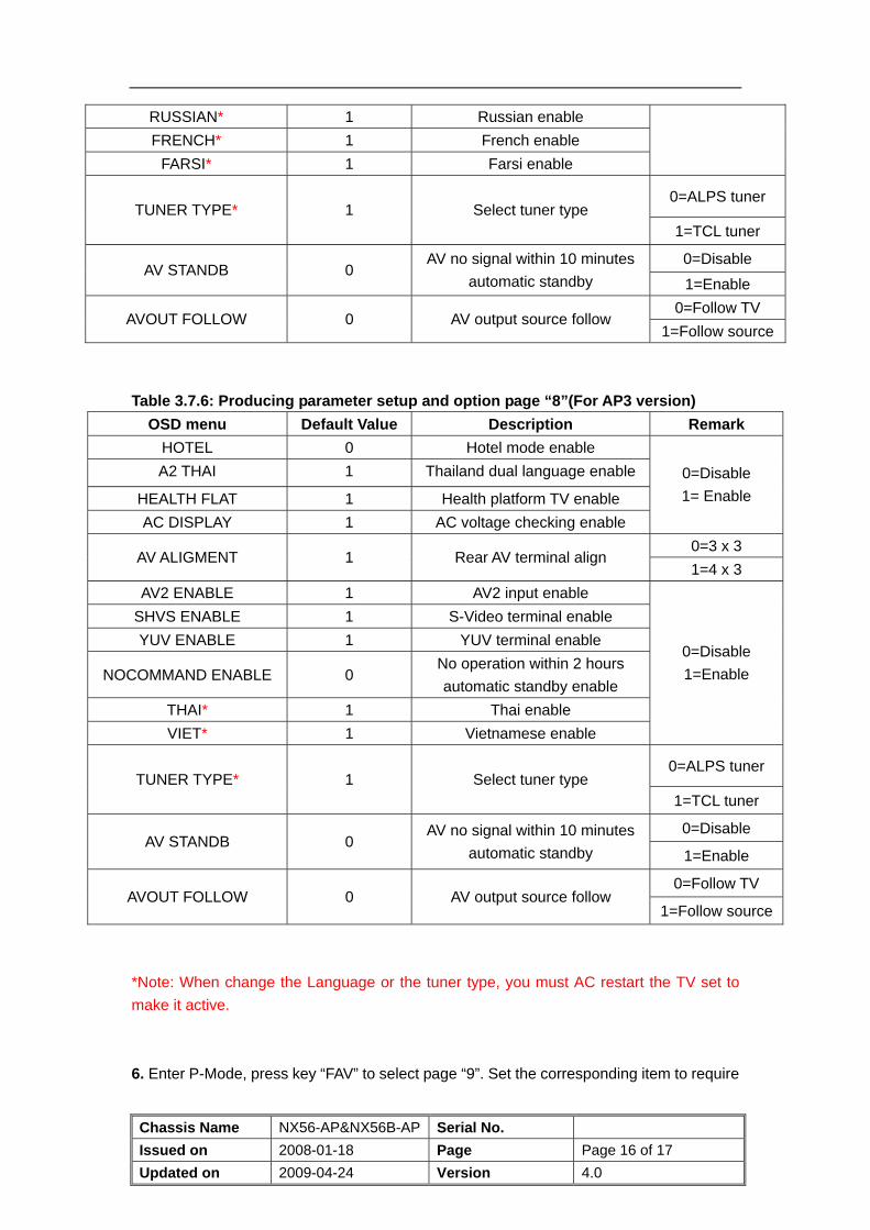
RUSSIAN* 1 Russian enable
FRENCH* 1 French enable
FARSI* 1 Farsi enable
0=ALPS tuner TUNER TYPE* 1 Select tuner type
1=TCL tuner
0=Disable AV STANDB 0
AV no signal within 10 minutes
automatic standby 1=Enable
0=Follow TV AVOUT FOLLOW 0 AV output source follow
1=Follow source
Table 3.7.6: Producing parameter setup and option page “8”(For AP3 version)
OSD menu Default Value Description Remark
HOTEL 0 Hotel mode enable
A2 THAI 1 Thailand dual language enable
HEALTH FLAT 1 Health platform TV enable
AC DISPLAY 1 AC voltage checking enable
0=Disable
1= Enable
0=3 x 3 AV ALIGMENT 1 Rear AV terminal align
1=4 x 3
AV2 ENABLE 1 AV2 input enable
SHVS ENABLE 1 S-Video terminal enable
YUV ENABLE 1 YUV terminal enable
NOCOMMAND ENABLE 0 No operation within 2 hours
automatic standby enable
THAI* 1 Thai enable
VIET* 1 Vietnamese enable
0=Disable
1=Enable
0=ALPS tuner TUNER TYPE* 1 Select tuner type
1=TCL tuner
0=Disable AV STANDB 0
AV no signal within 10 minutes
automatic standby 1=Enable
0=Follow TV AVOUT FOLLOW 0 AV output source follow
1=Follow source
*Note: When change the Language or the tuner type, you must AC restart the TV set to
make it active.
6. Enter P-Mode, press key “FAV” to select page “9”. Set the corresponding item to require
Chassis Name NX56-AP&NX56B-AP Serial No.
Issued on 2008-01-18 Page Page 17 of 17
Updated on 2009-04-24 Version 4.0
value. See below table 3.7.7 for detailed description.
Table 3.7.7: Producing parameter setup and option page “9”
OSD menu Default Value Description Remark
0=Disable BKS 1 Black stretch enable
1=Enable
0=15IRE BSD 0 Black Stretch depth
1=30IRE
0=12%
1=20%
2=6% AAS 0
Black area to switch off the
black stretch
3=8%
0=1:1
1=1.5:1 RPA 1 Ratio of pre- and after shoot
2=2:1
0=1:1
1=1:1.3
3=1:1.7 RPO 1
Ratio of positive and
negative peaks
4=1:0.7
0=0%
1=5%
2=10% SOC 2
Soft clipping level above
PWL
3=Soft clipping off
0=off
1= between 0 and 20 IRE
2= between 0 and 40 IRECOR 0 Video peaking active range
3= between 0 and 100 IRE
3.8 Screen voltage (VG2) adjustment with AKB function 1. Put the TV in AV source without input signal.
2. Enter P-Mode, press RC key "AT", there will display
3. Adjust the "SCREEN" VR of the FBT until VG2 hint display (LOW/OK/HIGH) display
"OK" stably.
4. Press “MENU” return to P-Mode.
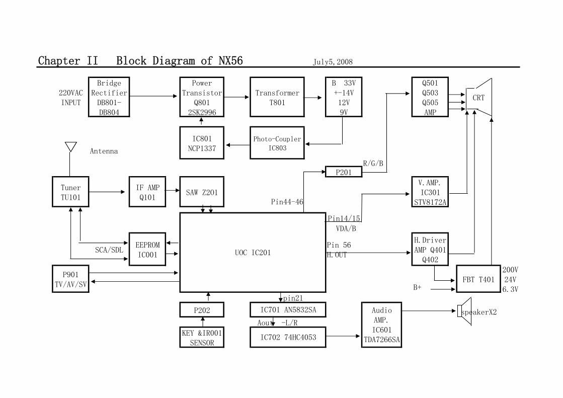
220VACINPUT
BridgeRectifierDB801-DB804
PowerTransistor
Q8012SK2996
TransformerT801
B 33V+-14V12V9V
Q501Q503Q505AMP
CRT
▽ Antenna
IC801NCP1337
Photo-CouplerIC803
R/G/BP201
TunerTU101
IF AMPQ101
SAW Z2O1Pin44-46
V.AMP.IC301
STV8172A
Pin14/15
VDA/B
SCA/SDLEEPROMIC001
Pin 56H.OUT
H.DriverAMP Q401Q402
P901TV/AV/SV B+
FBT T401200V24V6.3V
pin21
P202 speakerX2
Aout -L/R
KEY &IR001SENSOR
UOC IC201
Chapter II Block Diagram of NX56 July5,2008
AudioAMP.IC601
TDA7266SA
IC701 AN5832SA
IC702 74HC4053

NX56 Chassis Signal Processing Introduction
Brief introduction
For different market requirements, our design it in two versions, one is
for Latin America, we call the chassis as NX56-LA, the another one is for
Asia Pacific Area, we call the chassis as NX56-AP. NX56-LA and
NX56-AP adopt different UOC, The UOC for Latin America have
CCD-Chip and BTSC function, so added AN5832SA to realize BTSC,
but the UOC for Asia Pacific region does not have the two functions but
SECAM system is necessary. NX56 Chassis not only match 21inches
CRT, but also match 25 and 29inches CRT. Due to different screen sizes,
maybe adopt different audio power amplifiers. The others should be the
same. No matter NX56-AP what NX56-LA, they are use same main PCB
board, just different peripheral components.
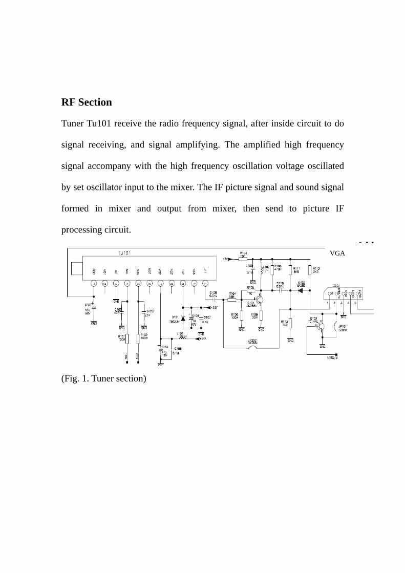
RF Section
Tuner Tu101 receive the radio frequency signal, after inside circuit to do
signal receiving, and signal amplifying. The amplified high frequency
signal accompany with the high frequency oscillation voltage oscillated
by set oscillator input to the mixer. The IF picture signal and sound signal
formed in mixer and output from mixer, then send to picture IF
processing circuit.
VGA
(Fig. 1. Tuner section)
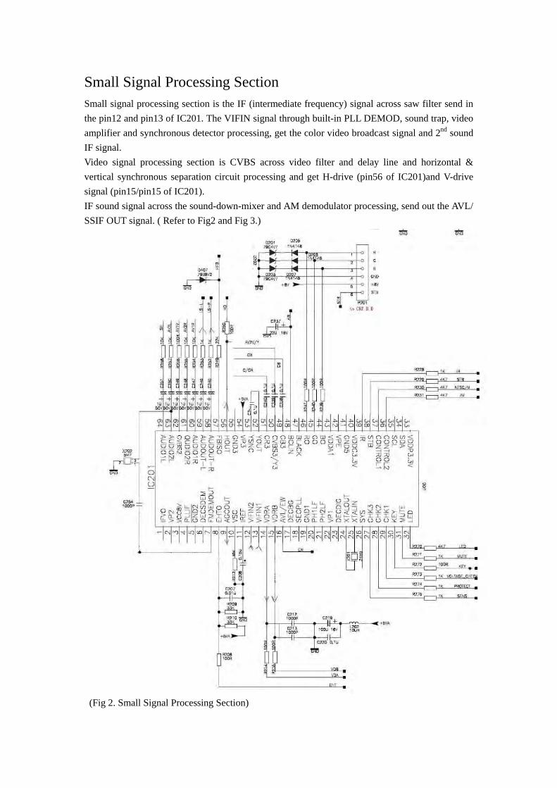
Small Signal Processing Section Small signal processing section is the IF (intermediate frequency) signal across saw filter send in the pin12 and pin13 of IC201. The VIFIN signal through built-in PLL DEMOD, sound trap, video amplifier and synchronous detector processing, get the color video broadcast signal and 2nd sound IF signal. Video signal processing section is CVBS across video filter and delay line and horizontal & vertical synchronous separation circuit processing and get H-drive (pin56 of IC201)and V-drive signal (pin15/pin15 of IC201). IF sound signal across the sound-down-mixer and AM demodulator processing, send out the AVL/ SSIF OUT signal. ( Refer to Fig2 and Fig 3.)
(Fig 2. Small Signal Processing Section)
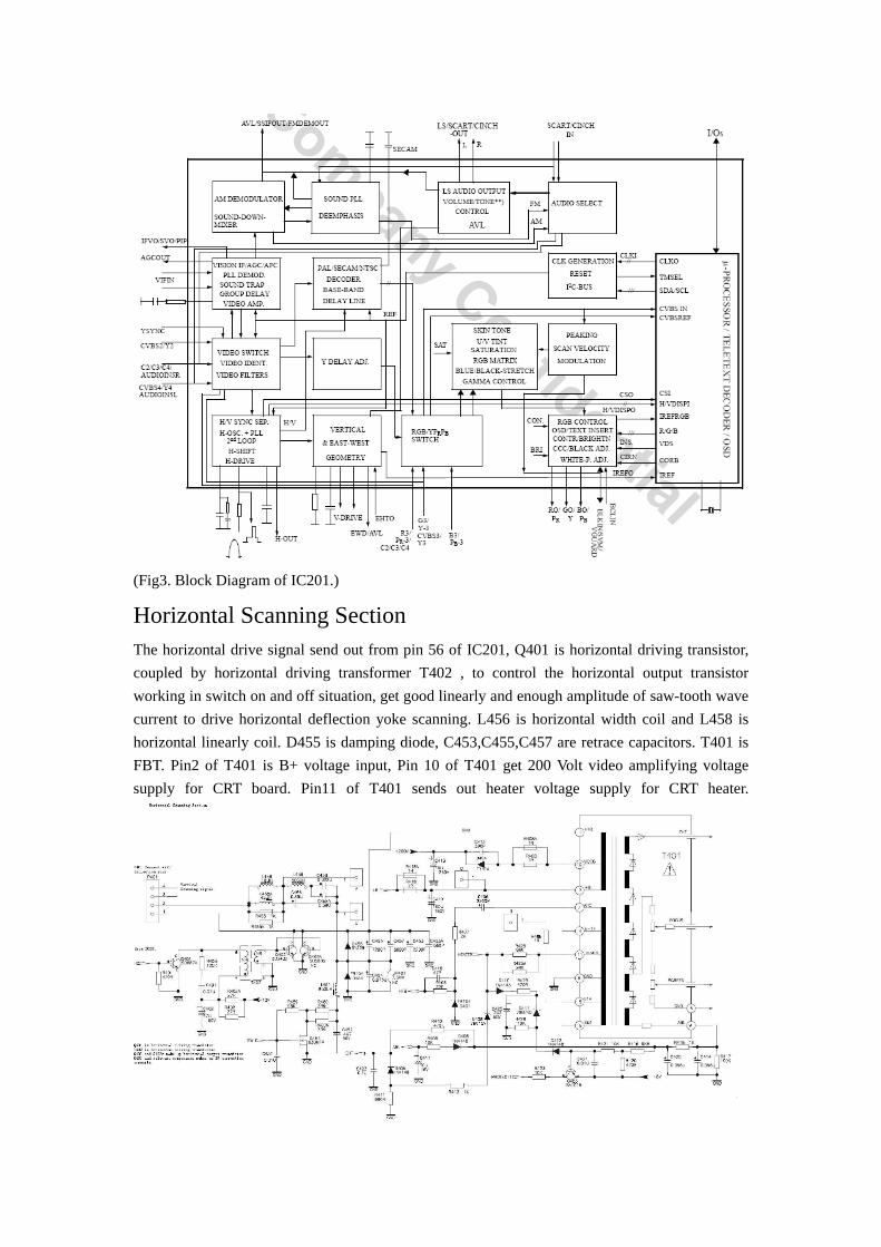
(Fig3. Block Diagram of IC201.)
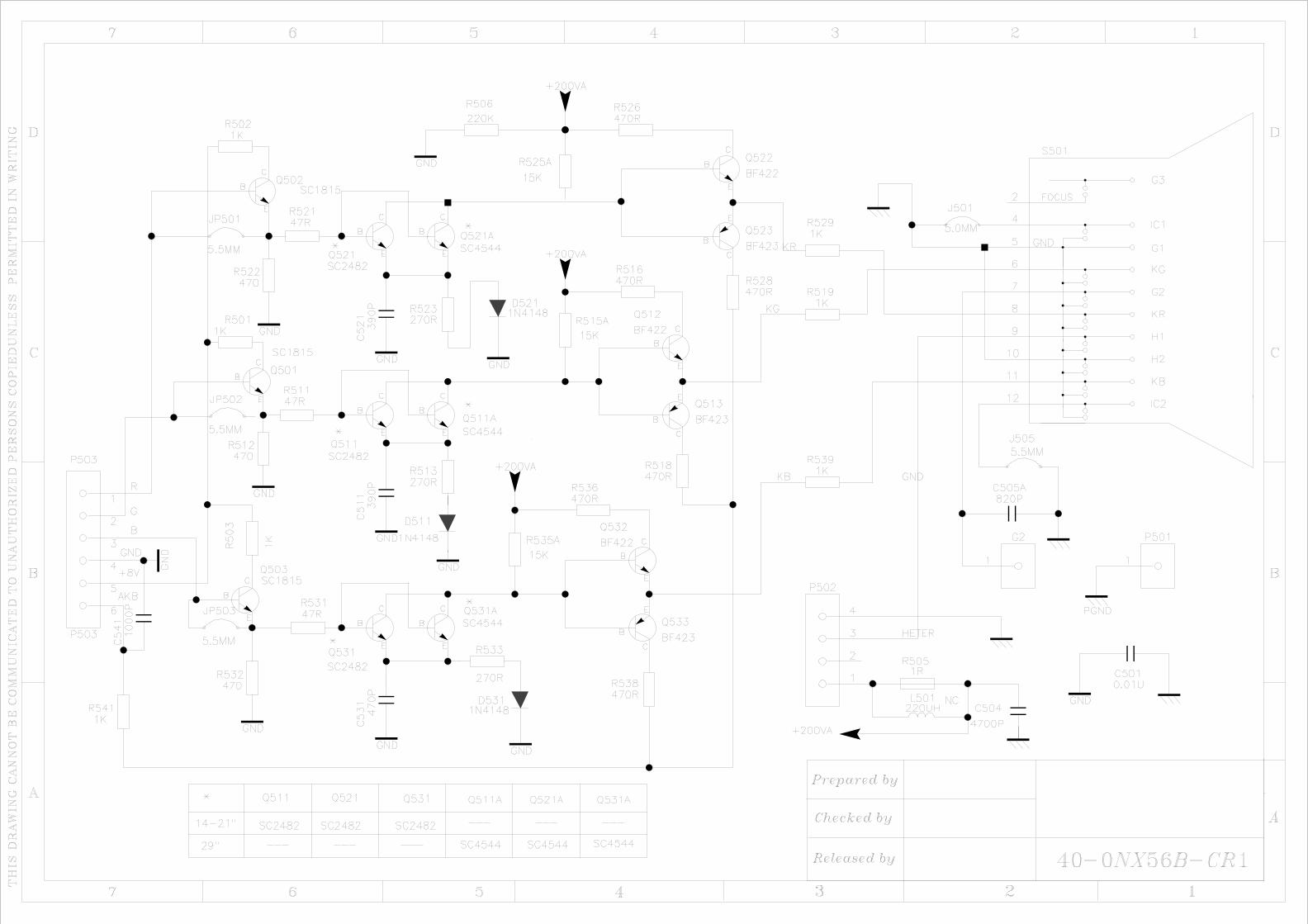
Horizontal Scanning Section The horizontal drive signal send out from pin 56 of IC201, Q401 is horizontal driving transistor, coupled by horizontal driving transformer T402 , to control the horizontal output transistor working in switch on and off situation, get good linearly and enough amplitude of saw-tooth wave current to drive horizontal deflection yoke scanning. L456 is horizontal width coil and L458 is horizontal linearly coil. D455 is damping diode, C453,C455,C457 are retrace capacitors. T401 is FBT. Pin2 of T401 is B+ voltage input, Pin 10 of T401 get 200 Volt video amplifying voltage supply for CRT board. Pin11 of T401 sends out heater voltage supply for CRT heater.
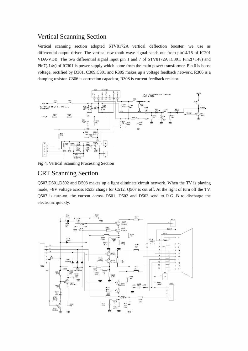
Vertical Scanning Section Vertical scanning section adopted STV8172A vertical deflection booster, we use as differential-output driver. The vertical raw-tooth wave signal sends out from pin14/15 of IC201 VDA/VDB. The two differential signal input pin 1 and 7 of STV8172A IC301. Pin2(+14v) and Pin7(-14v) of IC301 is power supply which come from the main power transformer. Pin 6 is boost voltage, rectified by D301. C309,C301 and R305 makes up a voltage feedback network, R306 is a damping resistor. C306 is correction capacitor, R308 is current feedback resistor.
Fig 4. Vertical Scanning Processing Section
CRT Scanning Section Q507,D501,D502 and D503 makes up a light eliminate circuit network. When the TV is playing mode, +8V voltage across R533 charge for C512, Q507 is cut off. At the right of turn off the TV, Q507 is turn-on, the current across D501, D502 and D503 send to R.G. B to discharge the electronic quickly.
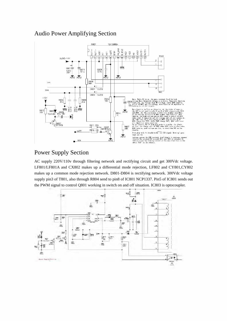
Audio Power Amplifying Section
Power Supply Section AC supply 220V/110v through filtering network and rectifying circuit and get 300Vdc voltage. LF801/LF801A and CX802 makes up a differential mode rejection, LF802 and CY801,CY802 makes up a common mode rejection network. D801-D804 is rectifying network. 300Vdc voltage supply pin3 of T801, also through R804 send to pin8 of IC801 NCP1337. Pin5 of IC801 sends out the PWM signal to control Q801 working in switch on and off situation. IC803 is optocoupler.


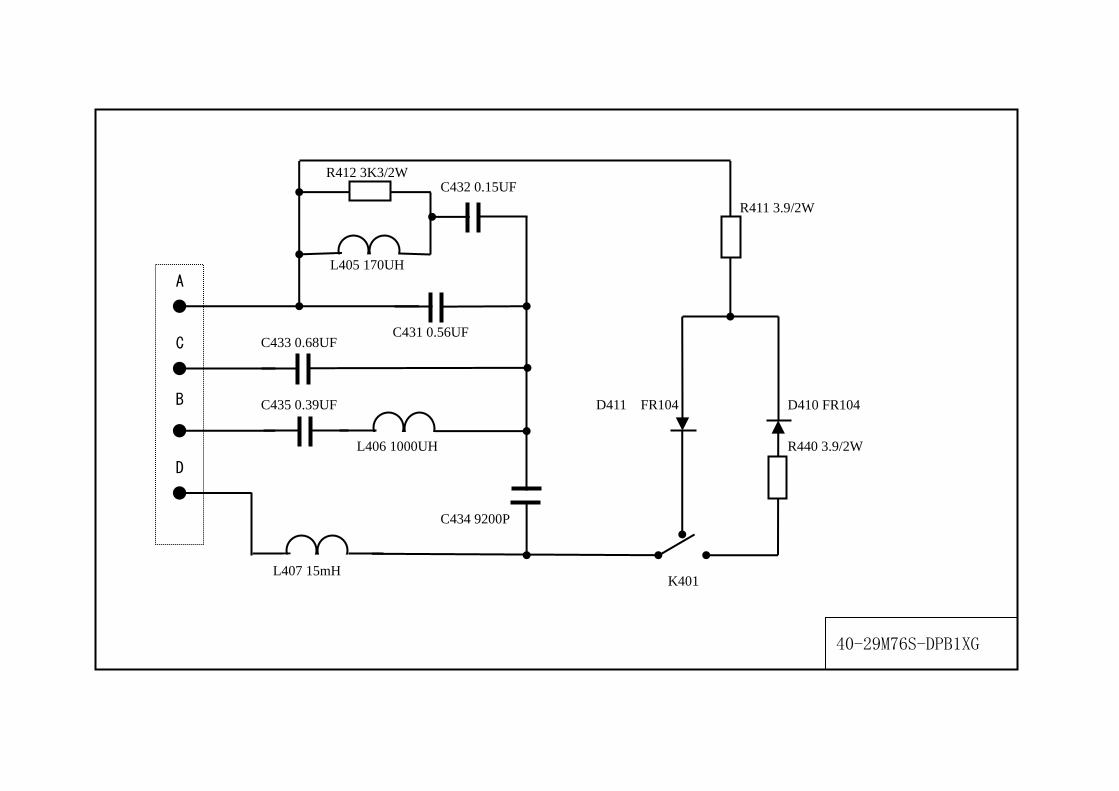
K401
40-29M76S-DPB1XG
A
C
B
D
R411 3.9/2W
R412 3K3/2W
L405 170UH
C432 0.15UF
C431 0.56UF C433 0.68UF
C435 0.39UF
L406 1000UH
L407 15mH
C434 9200P
D411 FR104 D410 FR104
R440 3.9/2W
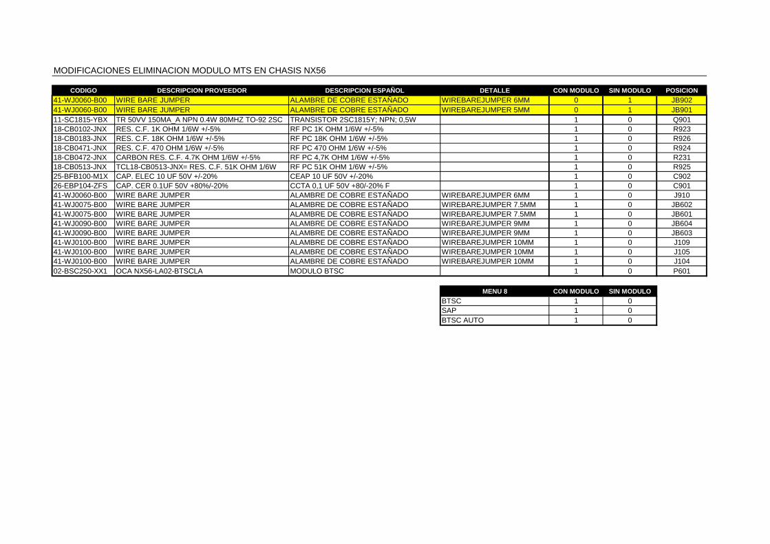
MODIFICACIONES ELIMINACION MODULO MTS EN CHASIS NX56
CODIGO DESCRIPCION PROVEEDOR DESCRIPCION ESPAÑOL DETALLE CON MODULO SIN MODULO POSICION
41-WJ0060-B00 WIRE BARE JUMPER ALAMBRE DE COBRE ESTAÑADO WIREBAREJUMPER 6MM 0 1 JB90241-WJ0060-B00 WIRE BARE JUMPER ALAMBRE DE COBRE ESTAÑADO WIREBAREJUMPER 5MM 0 1 JB90111-SC1815-YBX TR 50VV 150MA_A NPN 0.4W 80MHZ TO-92 2SC TRANSISTOR 2SC1815Y; NPN; 0,5W 1 0 Q90118-CB0102-JNX RES. C.F. 1K OHM 1/6W +/-5% RF PC 1K OHM 1/6W +/-5% 1 0 R92318-CB0183-JNX RES. C.F. 18K OHM 1/6W +/-5% RF PC 18K OHM 1/6W +/-5% 1 0 R92618-CB0471-JNX RES. C.F. 470 OHM 1/6W +/-5% RF PC 470 OHM 1/6W +/-5% 1 0 R92418-CB0472-JNX CARBON RES. C.F. 4.7K OHM 1/6W +/-5% RF PC 4,7K OHM 1/6W +/-5% 1 0 R23118-CB0513-JNX TCL18-CB0513-JNX= RES. C.F. 51K OHM 1/6W RF PC 51K OHM 1/6W +/-5% 1 0 R92525-BFB100-M1X CAP. ELEC 10 UF 50V +/-20% CEAP 10 UF 50V +/-20% 1 0 C90226-EBP104-ZFS CAP. CER 0.1UF 50V +80%/-20% CCTA 0,1 UF 50V +80/-20% F 1 0 C90141-WJ0060-B00 WIRE BARE JUMPER ALAMBRE DE COBRE ESTAÑADO WIREBAREJUMPER 6MM 1 0 J91041-WJ0075-B00 WIRE BARE JUMPER ALAMBRE DE COBRE ESTAÑADO WIREBAREJUMPER 7.5MM 1 0 JB60241-WJ0075-B00 WIRE BARE JUMPER ALAMBRE DE COBRE ESTAÑADO WIREBAREJUMPER 7.5MM 1 0 JB60141-WJ0090-B00 WIRE BARE JUMPER ALAMBRE DE COBRE ESTAÑADO WIREBAREJUMPER 9MM 1 0 JB60441-WJ0090-B00 WIRE BARE JUMPER ALAMBRE DE COBRE ESTAÑADO WIREBAREJUMPER 9MM 1 0 JB60341-WJ0100-B00 WIRE BARE JUMPER ALAMBRE DE COBRE ESTAÑADO WIREBAREJUMPER 10MM 1 0 J10941-WJ0100-B00 WIRE BARE JUMPER ALAMBRE DE COBRE ESTAÑADO WIREBAREJUMPER 10MM 1 0 J10541-WJ0100-B00 WIRE BARE JUMPER ALAMBRE DE COBRE ESTAÑADO WIREBAREJUMPER 10MM 1 0 J10402-BSC250-XX1 OCA NX56-LA02-BTSCLA MODULO BTSC 1 0 P601
MENU 8 CON MODULO SIN MODULO
BTSC 1 0SAP 1 0BTSC AUTO 1 0

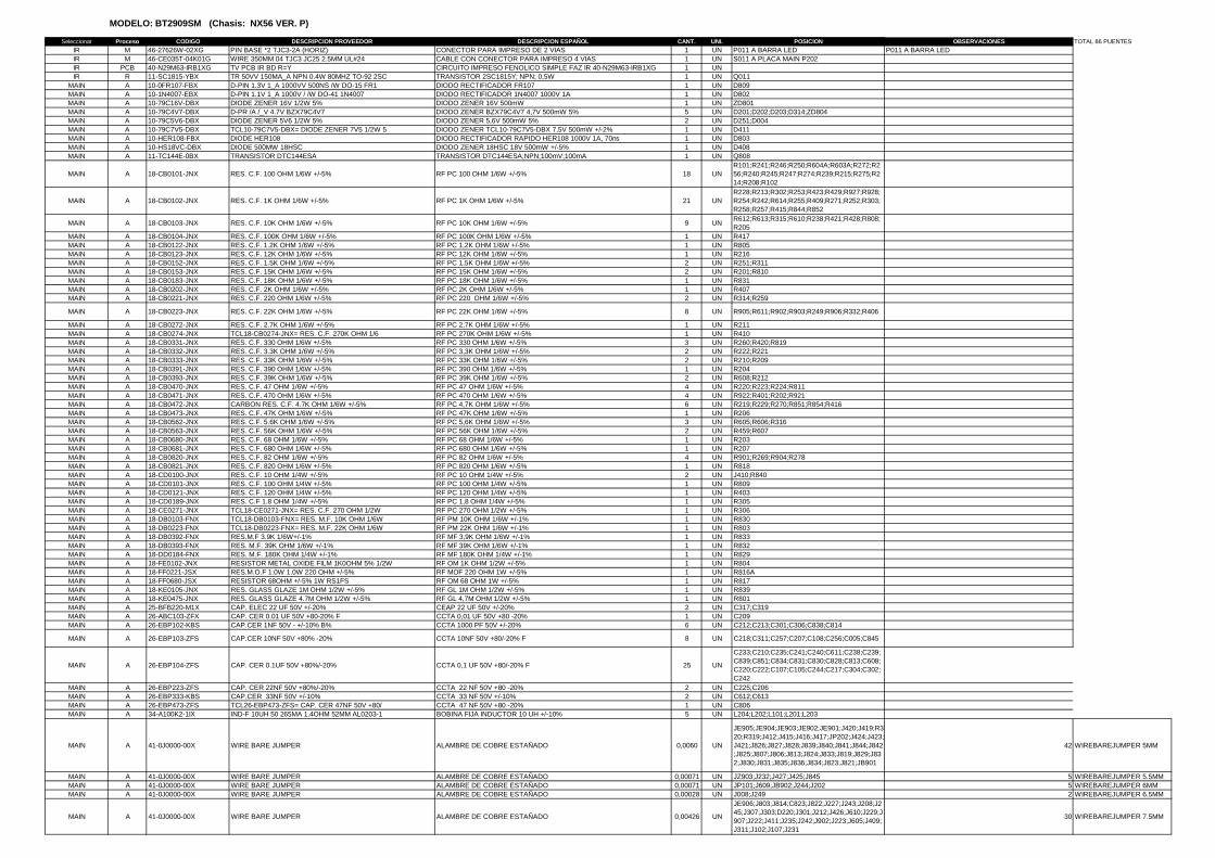
MODELO: BT2909SM (Chasis: NX56 VER. P)
Seleccionar Proceso CODIGO DESCRIPCION PROVEEDOR DESCRIPCION ESPAÑOL CANT. UNI. POSICION OBSERVACIONES TOTAL 86 PUENTES
A/V M 46-CD055T-05K01G WIRE 550MM 05 TJC3 SCN 2.5MM UL#246 CABLE CON CONECTOR PARA IMPRESO 5 VIAS 1 UN P1903 A P902A/V M 47-RCA020-XX1G RCA SOCKET Y/W/R CONECTOR PARA IMPRESO 90º 3 VIAS RCA (1XCVBS+AUDIO) 1 UN P1901A/V PCB 40-029M71-SIA1XG TV PCB SI BD R=Y CIRCUITO IMPRESO FENOLICO SIMPLE FAZ A/V LATERAL 40-029M71-SIA1XG1 UN
CONTROLES A 18-CB0102-JNX RES. C.F. 1K OHM 1/6W +/-5% RF PC 1K OHM 1/6W +/-5% 1 UN R1005CONTROLES A 18-CB0271-JNX RES. C.F. 270 OHM 1/6W +/-5% RF PC 270 OHM 1/6W +/-5% 1 UN R1003CONTROLES A 18-CB0331-JNX RES. C.F. 330 OHM 1/6W +/-5% RF PC 330 OHM 1/6W +/-5% 1 UN R1002CONTROLES A 18-CB0471-JNX RES. C.F. 470 OHM 1/6W +/-5% RF PC 470 OHM 1/6W +/-5% 1 UN R1001CONTROLES A 18-CB0561-JNX RES. C.F. 560 OHM 1/6W +/-5% RF PC 560 OHM 1/6W +/-5% 1 UN R006CONTROLES A 41-0J0000-00X WIRE BARE JUMPER ALAMBRE DE COBRE ESTAÑADO 0,00014 UN J1001 1 WIREBAREJUMPER 7.5MMCONTROLES M 46-CE060T-02K01G WIRE UL2468#26 600MM 2 2.5MM CABLE CON CONECTOR PARA IMPRESO 2 VIAS 1 UN P1003 A PLACA MAIN P204CONTROLES M 48-TAC002-XX0 TACT SWITCH LLAVE PULSADOR AL TACTO 6 UN K004;K005;K006;K001;K002;K003CONTROLES PCB 40-N29M71-KEG1XG TV PCB KEY BD R=Y CIRCUITO IMPRESO FENOLICO SIMPLE FAZ CONTROLES 40-N29M71-KEG1XG1 UN
DP A 10-0FR104-FBX DIODE FR104 (FAST RECTIFIER) DIODO RECTIFICADOR FR104 600V 1A 2 UN D411;D410
DP A 66-343730-0B0 HOLLOW RIVET 1.6MMX3.0MMX3.2MM OJALILLO DE LATON ESTAÑADO 1.6X3.0XL3.2 14 UNC433X2;C432X2;C431X2;L407X2;L406X2;L405X2;C434X2
DP A 66-343740-0B0 HOLLOW RIVET (2.3MMX4.0MMX3.5MM) OJALILLO DE LATON ESTAÑADO 2.3mmx4.0mmx3.5mm 4 UN P401X4DP M 18-FG0332-JHX RESISTOR METAL OXIDE FILM 3K3OHM 5% 2WW RF OM 3,3K OHM 2W +/-5% 1 UN R412DP M 18-FG0399-JHX RESISTOR METAL OXIDE FILM 3R9OHM 5% 2WW RF OM 3,9 OHM 2W +/-5% 2 UN R440;R411DP M 27-AGQ394-JSX TCL27-AGQ394-JSX= CAP. M.PP 0.39UF 250VA CCTA 0,39UF 250V +/-5% 1 UN C435DP M 27-AHQ154-JSX CAP. M.PP 0.15UF 400V +/-5% CCTA 0,15UF 400V +/-5% 1 UN C432DP M 27-AHR564-JSX CAP.M.PP 400V 560NF +/-5% CPP MYLAR 560 nF 400V +/-5% 1 UN C431DP M 27-AHR684-JSX CAP.PP 680NF 400V +/-5% CPP MYLAR 680NF 400V +/-5% 1 UN C433DP M 27-ALR912-J0X CAP. M.PP 9100 PF 1.6KV +/-5% CPP MYLAR 9100PF 400V +/-5% 1 UN C434DP M 36-WID102-XX1 COIL WIDTH 1 MH BOBINA FIJA DE ANCHO 1 MH 1 UN L406DP M 36-WID153-XX1 COIL CHOKE 15 MH BOBINA FIJA CHOQUE 15 MH 1 UN L407DP M 36-WID171-XX3 COIL WIDTH L171AHA BOBINA FIJA DE ANCHO L171AHA 1 UN L405DP M 46-39402W-04XG BASE CONECTOR PARA IMPRESO DE 4 VIAS 1 UN P401DP M 48-SLI001-XX0 SW. CHANNEL BAND SELECTOR KFC-G02 LLAVE SELECTORA 2 VIAS KFC-G02 60VDC 1 UN K401DP PCB 40-29M76S-DPB1XG TV PCB DP BD R=Y CIRCUITO IMPRESO FENOLICO SIMPLE FAZ COMP. HTAL 40-29M76S-DPB1XG1 UN
EMBALAJE E 74-022032-6WEEM PRI BAG -- RED 186C 01 00 00 R=N BOLSA PARA ACCESORIOS 1 UNEMBALAJE E 74-130130-80HEM DEC BAG 130X130CM RED 186C 00 EM 00 R=Y BOLSA PARA TELEVISOR CON ADV. DE SEGURIDAD 1 UNEMBALAJE E T6-016W31-AAR1X ASY - REMOTE LOGO:BGH FEELNOLOGY CONTROL REMOTO BGH FEELNOLOGY 1 UNENSAMBLE A 18-EE0109-JSX FR 1OHM 1/2W N RF10S RF 10 OHM 1/2W +/-5% 1 UN R465ENSAMBLE E 36-DEG290-XX2L DEGAUSSING COIL XC-29" BOBINA FIJA DESMAGNETIZADORA 1 UNENSAMBLE E 41-GND029-LX0 B121 MALLA DE ALAMBRE DE MASA TRC 29" 1 UNENSAMBLE E 42-61608F-XX1G SPEAKER YDP616-5A PARLANTE YDP616-5A 2 UN SP602;SP601ENSAMBLE E 46-26514H-04XG HS 4P A/B 500/13 RBGW TJC1-4Y CABLE CON CONECTOR 4P A/B 500/13 RBGW TJC1-4Y 1 UNENSAMBLE E 46-35197H-02XG HS 2P22 700/7 TJC3-2Y CABLE CON CONECTOR HEMBRA 2 VIAS TJC3-2Y 1 UN S601A A R_SPKENSAMBLE E 46-CT048T-03K01G WIRE CONNECT 480MM 3 TJC3 PH 2.5MM UL246 CABLE CON CONECTOR HEMBRA 3 VIAS 1 UN S602 A L_SPKENSAMBLE E 46-KN035T-03I01G WIRE ת½ÓÏß 350MM 3 VH 187×ÔËø 3.96MM UL CABLE CON CONECTOR PARA IMPRESO 2 VIAS 1 UN LLAVE ENCENDIDO A PLACA MAINENSAMBLE E 48-POW016-FX3G SWITH-POWER 128V 8A HF-606(TV)-¢ó LLAVE MECANICA DE RED 128 VCA 8A HF-606 1 UNENSAMBLE E 51-DC0220-0QT0HG POWER CORD 2200MM 187 Y DTI-2P-08 CABLE DE ALIMENTACION CON FICHA 220V DTI-2P-08 1 UNENSAMBLE E 54-113970-0U0 TV RAW INSULATOR SLEEVE AWG#5 -- 00 00 R TUBO SPAGHETTI DE PVC 0,32 M CABLE PARLANTESENSAMBLE E 54-114000-00X TV RAW FELT PAPER 150MMX19MMX0.3MM BK 01 FIELTRO AUTOADHESIVO (150mmX19mmX0,3mm) 9 UN MTJE. TRC A FRENTEENSAMBLE E 54-114000-00X TV RAW FELT PAPER 150MMX19MMX0.3MM BK 01 FIELTRO AUTOADHESIVO (150mmX19mmX0,3mm) 4 UN TAPA TRASERAENSAMBLE E 54-205140-000 SPACER CRT MOUNTING T=2MM ESPACIADOR DE GOMA E=2mm 4 UN MTJE. TRC A FRENTEENSAMBLE E 54-314740-0X0 CRT FIBRE SHEET (22MMX22MMX0.8MM) AMORTIGUADOR DE FIBRA (22mmX22mmX0.8mm) 12 UN MTJE. TRC A FRENTEENSAMBLE E 55-BM62RC-5CL6R DEC BACKCOVER -- A8252 01 00 00 R=N TAPA TRASERA BT2909S 1 UN INCLUYE FIELTRO AUTOADHESIVO X6ENSAMBLE E 56-445230-4HN6R TV PRI FASTENER CABLE-STRAP -- 00 00 R=N SOPORTE PLASTICO LATERAL PARA PLACA A/V 1 UNENSAMBLE E 56-LM62FB-1HA5C TV DEC KEY CLUSTER 29M71 -- 01 5C 00 R=N CONJUNTO DE TECLAS PLASTICAS 1 UNENSAMBLE E 57-10654X-00F TWIST TIE NY66 LAZO PLASTICO 5 UNENSAMBLE E 57-445670-0HC02 TV DEC DECOR LUMINOUS BAR -- 00 02 00 R= BARRA LUMINOSA CON LEDS 1 UNENSAMBLE E 58-456790-1UI1A TV DEC OVERLAY 29A41 REAR AV OVERLAY TO ETIQUETA CONECTORES TRASEROS BT2909S 1 UNENSAMBLE E 58-BM63MP-0UI9J DEC OVERLAY -- WHITE & BLACK 00 00 R=Y ETIQUETA IDENTIFICACION BT2909SM 1 UNENSAMBLE E 59-377680-000 RUBBER PAD (22X22X5MM) PATA DE GOMA 22X22X5MM 2 UN MTJE TRCENSAMBLE E 62-216340-0UN TCL62-216340-0UN= BLOCK R=N TRABA PLASTICA SUJETA CABLE 1 UNENSAMBLE E 62-321780-0HG TV RAW FASTENER CRT DEGAUSSING COIL 25"" SUJETADOR PLASTICO PARA BOBINA DESMAGNETIZANTE 4 UNENSAMBLE E 63-B40150-AB4G SCREW-ST 4MM 15MM ISO 62 R=Y TORNILLO PARA PLASTICO ZINCADO W 4 X 15 1 UN MTJE. FLY BACK A TAPA TRASERAENSAMBLE E 63-B40200-AB3G SCREW-ST 4MM 20MM JIS B 1122 12 R=Y TORNILLO PARA PLASTICO ZINCADO B 4 X 20 AB 10 UN CERRADO DEL TVENSAMBLE E 63-F30100-BT3G SCREW-ST 3MM 10MM ISO 65 0 0 R=Y TORNILLO PARA PLASTICO ZINCADO NEGRO W 3 X 10 AB 2 UN MTJE. CONECTORES TRASEROS A TAPA TRASERAENSAMBLE E 63-S40120-BT4G MACHINE SCREW TORNILLO PARA PLASTICO C/ALA ZINCADO 4 X 12 4 UN MTJE. PARLANTES A FRENTEENSAMBLE E 63-W30100-AB4G S/T SCREW W 3 X 10 AB TORNILLO PARA PLASTICO ZINCADO W 3 X 10 AB 2 UN MTJE. PLACA CONTROLES A FRENTE
ENSAMBLE E 63-W30120-AB4G S/T SCREW W 3 X 12 AB TORNILLO PARA PLASTICO ZINCADO W 3 X 12 AB 4 UNMTJE. A/V LATERAL A FRENTEX2; MTJE. PLACA CONTROLES A FRENTE
ENSAMBLE E 63-Z60300-AB4G S/T SCREW HA 6X30 TORNILLO PARA PLASTICO ZINCADO 6 X 30 4 UN MTJE. TRCENSAMBLE E 67-X21679-0E0 SPRING CRT 6MMX50MMX0.6MM RESORTE DE ACERO TRC 2 UNENSAMBLE E 71-TELEFU-LAB9A TV PRI LABEL 14E10 WHIT & BLACK R=N ETIQUETA ADVERTENCIA PARA EL USUARIO 1 UN PARA CABLE DE ALIMENTACIONENSAMBLE E 90-0DLSG1-JY1U SILICON GREASE DLSG-1 GRASA SILICONADA DLSG-1 0,373 GENSAMBLE M 13-TDA121-65P IC-CHIPSET MCU(WRITE) CI MICROPROCESADOR TDA12165 1 UN IC201(CP)ENSAMBLE M 46-33079W-05XG PIN BASE *5 TJC3-5A CONECTOR PARA IMPRESO DE 5 VIAS 1 UN P902
FRENTE E 55-BV18FC-1CL6L DEC BACKCOVER -- Q0003 01 6L 00 R=N FRENTE BT2909S 1 UNFRENTE E 55-BV18MC-0CL9K DEC BACKCOVER -- Q0001 01 9K 00 R=N FRENTE DECORATIVO BT2909S 1 UNFRENTE E 56-B266LE-0HC5Z TV EQU KEY S29M63 SILVER R=N LENTE ACRILICA IR 1 UNFRENTE E 58-LM62FI-3UI9G TV DEC OVERLAY BM62 -- 00 00 00 R=Y ETIQUETA CONTROLES LATERALES 1 UNFRENTE E 59-130460-00X RUBBER PAD (25MMX7MM) PATA DE GOMA 25MMX7MM 2 UN PEGADO EN FRENTEFRENTE E 62-407210-0UN POWER SUPPLY BRACKET SOPORTE PLASTICO PLACA DP 1 UNFRENTE E 62-444980-0CN CRT SUPPORT SOPORTE PLASTICO PARA TRC 2 UNFRENTE E 62-455090-0UN TV RAW BRACKET -- -- 00 00 R=N GUIA PLASTICA LATERAL PARA PLACA 2 UNFRENTE E 62-455100-0UN TV RAW BRACKET -- -- 00 00 R=N GUIA PLASTICA FRONTAL PARA PLACA 1 UNFRENTE E 63-B40150-AB4G SCREW-ST 4MM 15MM ISO 62 R=Y TORNILLO PARA PLASTICO ZINCADO W 4 X 15 2 UN MTJE. SOPORTES TRCFRENTE E 63-W30100-AB4G S/T SCREW W 3 X 10 AB TORNILLO PARA PLASTICO ZINCADO W 3 X 10 AB 1 UN MTJE. LENTE A FRENTEFRENTE E 63-W30100-AB4G S/T SCREW W 3 X 10 AB TORNILLO PARA PLASTICO ZINCADO W 3 X 10 AB 2 UN MTJE. BARRA LED A FRENTEFRENTE E 63-W30120-AB4G S/T SCREW W 3 X 12 AB TORNILLO PARA PLASTICO ZINCADO W 3 X 12 AB 12 UN MTJE. FRENTE DECORATIVO A FRENTEFRENTE E 67-L46201-0A09A DEC LOGO BGH FEELNOLOGY -- 00 9A 00 R=Y PLACA DE MARCA BGH FEELNOLOGY 29" 1 UN
IR A 18-CB0100-JNX RES. C.F. 10 OHM 1/6W +/-5% RF PC 10 OHM 1/6W +/-5% 1 UN R011IR A 18-CB0103-JNX RES. C.F. 10K OHM 1/6W +/-5% RF PC 10K OHM 1/6W +/-5% 1 UN R013IR A 18-CB0221-JNX RES. C.F. 220 OHM 1/6W +/-5% RF PC 220 OHM 1/6W +/-5% 1 UN R012IR A 25-BDB470-M1X CAP.ELE 5MM 47UF 25VV 5X11 85 / CEAP 47 UF 25V +/-20% 1 UN C012IR A 26-EBP104-ZFS CAP. CER 0.1UF 50V +80%/-20% CCTA 0,1 UF 50V +80/-20% F 1 UN C011IR M 02-IRR001-XX1T IR RECEIVER 37.9KHZ 5V N HM338A RECEPTOR INFRARROJO HM338A 1 UN IR011
MODELO: BT2909SM (Chasis: NX56 VER. P)
Seleccionar Proceso CODIGO DESCRIPCION PROVEEDOR DESCRIPCION ESPAÑOL CANT. UNI. POSICION OBSERVACIONES TOTAL 86 PUENTES
IR M 46-27626W-02XG PIN BASE *2 TJC3-2A (HORIZ) CONECTOR PARA IMPRESO DE 2 VIAS 1 UN P011 A BARRA LED P011 A BARRA LEDIR M 46-CE035T-04K01G WIRE 350MM 04 TJC3 JC25 2.5MM UL#24 CABLE CON CONECTOR PARA IMPRESO 4 VIAS 1 UN S011 A PLACA MAIN P202IR PCB 40-N29M63-IRB1XG TV PCB IR BD R=Y CIRCUITO IMPRESO FENOLICO SIMPLE FAZ IR 40-N29M63-IRB1XG 1 UNIR R 11-SC1815-YBX TR 50VV 150MA_A NPN 0.4W 80MHZ TO-92 2SC TRANSISTOR 2SC1815Y; NPN; 0,5W 1 UN Q011
MAIN A 10-0FR107-FBX D-PIN 1.3V 1_A 1000VV 500NS /W DO-15 FR1 DIODO RECTIFICADOR FR107 1 UN D809MAIN A 10-1N4007-EBX D-PIN 1.1V 1_A 1000V / /W DO-41 1N4007 DIODO RECTIFICADOR 1N4007 1000V 1A 1 UN D802MAIN A 10-79C16V-DBX DIODE ZENER 16V 1/2W 5% DIODO ZENER 16V 500mW 1 UN ZD801MAIN A 10-79C4V7-DBX D-PR /A /_V 4.7V BZX79C4V7 DIODO ZENER BZX79C4V7 4,7V 500mW 5% 5 UN D201;D202;D203;D314;ZD804MAIN A 10-79C5V6-DBX DIODE ZENER 5V6 1/2W 5% DIODO ZENER 5,6V 500mW 5% 2 UN D251;D004MAIN A 10-79C7V5-DBX TCL10-79C7V5-DBX= DIODE ZENER 7V5 1/2W 5 DIODO ZENER TCL10-79C7V5-DBX 7,5V 500mW +/-2% 1 UN D411MAIN A 10-HER108-FBX DIODE HER108 DIODO RECTIFICADOR RAPIDO HER108 1000V 1A, 70ns 1 UN D803MAIN A 10-HS18VC-DBX DIODE 500MW 18HSC DIODO ZENER 18HSC 18V 500mW +/-5% 1 UN D408MAIN A 11-TC144E-0BX TRANSISTOR DTC144ESA TRANSISTOR DTC144ESA;NPN;100mV;100mA 1 UN Q808
MAIN A 18-CB0101-JNX RES. C.F. 100 OHM 1/6W +/-5% RF PC 100 OHM 1/6W +/-5% 18 UNR101;R241;R246;R250;R604A;R603A;R272;R256;R240;R245;R247;R274;R239;R215;R275;R214;R208;R102
MAIN A 18-CB0102-JNX RES. C.F. 1K OHM 1/6W +/-5% RF PC 1K OHM 1/6W +/-5% 21 UNR228;R213;R302;R253;R423;R429;R927;R928;R254;R242;R614;R255;R409;R271;R252;R303;R258;R257;R415;R844;R852
MAIN A 18-CB0103-JNX RES. C.F. 10K OHM 1/6W +/-5% RF PC 10K OHM 1/6W +/-5% 9 UNR612;R613;R315;R610;R238;R421;R428;R808;R205
MAIN A 18-CB0104-JNX RES. C.F. 100K OHM 1/6W +/-5% RF PC 100K OHM 1/6W +/-5% 1 UN R417MAIN A 18-CB0122-JNX RES. C.F. 1.2K OHM 1/6W +/-5% RF PC 1,2K OHM 1/6W +/-5% 1 UN R805MAIN A 18-CB0123-JNX RES. C.F. 12K OHM 1/6W +/-5% RF PC 12K OHM 1/6W +/-5% 1 UN R216MAIN A 18-CB0152-JNX RES. C.F. 1.5K OHM 1/6W +/-5% RF PC 1,5K OHM 1/6W +/-5% 2 UN R251;R311MAIN A 18-CB0153-JNX RES. C.F. 15K OHM 1/6W +/-5% RF PC 15K OHM 1/6W +/-5% 2 UN R201;R810MAIN A 18-CB0183-JNX RES. C.F. 18K OHM 1/6W +/-5% RF PC 18K OHM 1/6W +/-5% 1 UN R831MAIN A 18-CB0202-JNX RES. C.F. 2K OHM 1/6W +/-5% RF PC 2K OHM 1/6W +/-5% 1 UN R407MAIN A 18-CB0221-JNX RES. C.F. 220 OHM 1/6W +/-5% RF PC 220 OHM 1/6W +/-5% 2 UN R314;R259
MAIN A 18-CB0223-JNX RES. C.F. 22K OHM 1/6W +/-5% RF PC 22K OHM 1/6W +/-5% 8 UN R905;R611;R902;R903;R249;R906;R332;R406
MAIN A 18-CB0272-JNX RES. C.F. 2.7K OHM 1/6W +/-5% RF PC 2,7K OHM 1/6W +/-5% 1 UN R211MAIN A 18-CB0274-JNX TCL18-CB0274-JNX= RES. C.F. 270K OHM 1/6 RF PC 270K OHM 1/6W +/-5% 1 UN R410MAIN A 18-CB0331-JNX RES. C.F. 330 OHM 1/6W +/-5% RF PC 330 OHM 1/6W +/-5% 3 UN R260;R420;R819MAIN A 18-CB0332-JNX RES. C.F. 3.3K OHM 1/6W +/-5% RF PC 3,3K OHM 1/6W +/-5% 2 UN R222;R221MAIN A 18-CB0333-JNX RES. C.F. 33K OHM 1/6W +/-5% RF PC 33K OHM 1/6W +/-5% 2 UN R210;R209MAIN A 18-CB0391-JNX RES. C.F. 390 OHM 1/6W +/-5% RF PC 390 OHM 1/6W +/-5% 1 UN R204MAIN A 18-CB0393-JNX RES. C.F. 39K OHM 1/6W +/-5% RF PC 39K OHM 1/6W +/-5% 2 UN R608;R212MAIN A 18-CB0470-JNX RES. C.F. 47 OHM 1/6W +/-5% RF PC 47 OHM 1/6W +/-5% 4 UN R220;R223;R224;R811MAIN A 18-CB0471-JNX RES. C.F. 470 OHM 1/6W +/-5% RF PC 470 OHM 1/6W +/-5% 4 UN R922;R401;R202;R921MAIN A 18-CB0472-JNX CARBON RES. C.F. 4.7K OHM 1/6W +/-5% RF PC 4,7K OHM 1/6W +/-5% 6 UN R219;R229;R270;R851;R854;R416MAIN A 18-CB0473-JNX RES. C.F. 47K OHM 1/6W +/-5% RF PC 47K OHM 1/6W +/-5% 1 UN R206MAIN A 18-CB0562-JNX RES. C.F. 5.6K OHM 1/6W +/-5% RF PC 5,6K OHM 1/6W +/-5% 3 UN R605;R606;R316MAIN A 18-CB0563-JNX RES. C.F. 56K OHM 1/6W +/-5% RF PC 56K OHM 1/6W +/-5% 2 UN R459;R607MAIN A 18-CB0680-JNX RES. C.F. 68 OHM 1/6W +/-5% RF PC 68 OHM 1/6W +/-5% 1 UN R203MAIN A 18-CB0681-JNX RES. C.F. 680 OHM 1/6W +/-5% RF PC 680 OHM 1/6W +/-5% 1 UN R207MAIN A 18-CB0820-JNX RES. C.F. 82 OHM 1/6W +/-5% RF PC 82 OHM 1/6W +/-5% 4 UN R901;R269;R904;R278MAIN A 18-CB0821-JNX RES. C.F. 820 OHM 1/6W +/-5% RF PC 820 OHM 1/6W +/-5% 1 UN R818MAIN A 18-CD0100-JNX RES. C.F. 10 OHM 1/4W +/-5% RF PC 10 OHM 1/4W +/-5% 2 UN J410;R840MAIN A 18-CD0101-JNX RES. C.F. 100 OHM 1/4W +/-5% RF PC 100 OHM 1/4W +/-5% 1 UN R809MAIN A 18-CD0121-JNX RES. C.F. 120 OHM 1/4W +/-5% RF PC 120 OHM 1/4W +/-5% 1 UN R403MAIN A 18-CD0189-JNX RES. C.F 1.8 OHM 1/4W +/-5% RF PC 1,8 OHM 1/4W +/-5% 1 UN R305MAIN A 18-CE0271-JNX TCL18-CE0271-JNX= RES. C.F. 270 OHM 1/2W RF PC 270 OHM 1/2W +/-5% 1 UN R306MAIN A 18-DB0103-FNX TCL18-DB0103-FNX= RES. M.F. 10K OHM 1/6W RF PM 10K OHM 1/6W +/-1% 1 UN R830MAIN A 18-DB0223-FNX TCL18-DB0223-FNX= RES. M.F. 22K OHM 1/6W RF PM 22K OHM 1/6W +/-1% 1 UN R803MAIN A 18-DB0392-FNX RES.M.F 3.9K 1/6W+/-1% RF MF 3,9K OHM 1/6W +/-1% 1 UN R833MAIN A 18-DB0393-FNX RES. M.F. 39K OHM 1/6W +/-1% RF MF 39K OHM 1/6W +/-1% 1 UN R832MAIN A 18-DD0184-FNX RES. M.F. 180K OHM 1/4W +/-1% RF MF 180K OHM 1/4W +/-1% 1 UN R829MAIN A 18-FE0102-JNX RESISTOR METAL OXIDE FILM 1K0OHM 5% 1/2W RF OM 1K OHM 1/2W +/-5% 1 UN R804MAIN A 18-FF0221-JSX RES.M.O.F 1.0W 1.0W 220 OHM +/-5% RF MOF 220 OHM 1W +/-5% 1 UN R816AMAIN A 18-FF0680-JSX RESISTOR 68OHM +/-5% 1W RS1FS RF OM 68 OHM 1W +/-5% 1 UN R817MAIN A 18-KE0105-JNX RES. GLASS GLAZE 1M OHM 1/2W +/-5% RF GL 1M OHM 1/2W +/-5% 1 UN R839MAIN A 18-KE0475-JNX RES. GLASS GLAZE 4.7M OHM 1/2W +/-5% RF GL 4,7M OHM 1/2W +/-5% 1 UN R801MAIN A 25-BFB220-M1X CAP. ELEC 22 UF 50V +/-20% CEAP 22 UF 50V +/-20% 2 UN C317;C319MAIN A 26-ABC103-ZFX CAP. CER 0.01 UF 50V +80-20% F CCTA 0,01 UF 50V +80 -20% 1 UN C209MAIN A 26-EBP102-KBS CAP.CER 1NF 50V - +/-10% B% CCTA 1000 PF 50V +/-20% 6 UN C212;C213;C301;C306;C838;C814
MAIN A 26-EBP103-ZFS CAP.CER 10NF 50V +80% -20% CCTA 10NF 50V +80/-20% F 8 UN C218;C311;C257;C207;C108;C256;C005;C845
MAIN A 26-EBP104-ZFS CAP. CER 0.1UF 50V +80%/-20% CCTA 0,1 UF 50V +80/-20% F 25 UN
C233;C210;C235;C241;C240;C611;C238;C239;C839;C851;C834;C831;C830;C828;C813;C608;C220;C222;C107;C105;C244;C217;C304;C302;C242
MAIN A 26-EBP223-ZFS CAP. CER 22NF 50V +80%/-20% CCTA 22 NF 50V +80 -20% 2 UN C225;C206MAIN A 26-EBP333-KBS CAP.CER 33NF 50V +/-10% CCTA 33 NF 50V +/-10% 2 UN C612;C613MAIN A 26-EBP473-ZFS TCL26-EBP473-ZFS= CAP. CER 47NF 50V +80/ CCTA 47 NF 50V +80 -20% 1 UN C806MAIN A 34-A100K2-1IX IND-F 10UH 50 265MA 1.4OHM 52MM AL0203-1 BOBINA FIJA INDUCTOR 10 UH +/-10% 5 UN L204;L202;L101;L201;L203
MAIN A 41-0J0000-00X WIRE BARE JUMPER ALAMBRE DE COBRE ESTAÑADO 0,0060 UN
JE905;JE904;JE903;JE902;JE901;J420;J419;R320;R319;J412;J415;J416;J417;JP202;J424;J423;J421;J826;J827;J828;J839;J840;J841;J844;J842;J825;J807;J806;J813;J824;J833;J819;J829;J832;J830;J831;J835;J836;J834;J823;J821;JB901
42 WIREBAREJUMPER 5MM
MAIN A 41-0J0000-00X WIRE BARE JUMPER ALAMBRE DE COBRE ESTAÑADO 0,00071 UN JZ903;J232;J427;J425;J845 5 WIREBAREJUMPER 5.5MMMAIN A 41-0J0000-00X WIRE BARE JUMPER ALAMBRE DE COBRE ESTAÑADO 0,00071 UN JP101;J609;JB902;J244;J202 5 WIREBAREJUMPER 6MMMAIN A 41-0J0000-00X WIRE BARE JUMPER ALAMBRE DE COBRE ESTAÑADO 0,00028 UN J008;J249 2 WIREBAREJUMPER 6.5MM
MAIN A 41-0J0000-00X WIRE BARE JUMPER ALAMBRE DE COBRE ESTAÑADO 0,00426 UN
JE906;J803;J814;C823;J822;J227;J243;J208;J245;J307;J303;D220;J301;J212;J426;J610;J229;J907;J222;J411;J235;J242;J902;J223;J605;J409;J311;J102;J107;J231
30 WIREBAREJUMPER 7.5MM

MODELO: BT2909SM (Chasis: NX56 VER. P)
Seleccionar Proceso CODIGO DESCRIPCION PROVEEDOR DESCRIPCION ESPAÑOL CANT. UNI. POSICION OBSERVACIONES TOTAL 86 PUENTES
MAIN A 41-0J0000-00X WIRE BARE JUMPER ALAMBRE DE COBRE ESTAÑADO 0,00014 UN J007 1 WIREBAREJUMPER 8MM
MAIN A 41-0J0000-00X WIRE BARE JUMPER ALAMBRE DE COBRE ESTAÑADO 0,00156 UNJ913;J309;J915;J305;J914;J310;J228;J602;J214;J904;J837
11 WIREBAREJUMPER 8,5MM
MAIN A 41-0J0000-00X WIRE BARE JUMPER ALAMBRE DE COBRE ESTAÑADO 0,00028 UN J234;J221 2 WIREBAREJUMPER 9MMMAIN A 41-0J0000-00X WIRE BARE JUMPER ALAMBRE DE COBRE ESTAÑADO 0,00043 UN J403;J809;J810 3 WIREBAREJUMPER 9.5MM
MAIN A 41-0J0000-00X WIRE BARE JUMPER ALAMBRE DE COBRE ESTAÑADO 0,00426 UN
J001;J248;J246;J002;J108;J226;J207;J225;J230;J205;J206;J308;J414;J110;J607;J606;J237;J238;J601;J101;J201;J220;J247;J911;R004;JP809;JP808;JP807;J801;J802
30 WIREBAREJUMPER 10MM
MAIN A 41-0J0000-00X WIRE BARE JUMPER ALAMBRE DE COBRE ESTAÑADO 0,00014 UN J413 1 WIREBAREJUMPER 10.5MMMAIN A 41-0J0000-00X WIRE BARE JUMPER ALAMBRE DE COBRE ESTAÑADO 0,00028 UN J407; J908 2 WIREBAREJUMPER 11MMMAIN A 41-0J0000-00X WIRE BARE JUMPER ALAMBRE DE COBRE ESTAÑADO 0,00085 UN J916;J219;J215;J216;J217;J218 6 WIREBAREJUMPER 11.5MMMAIN A 41-0J0000-00X WIRE BARE JUMPER ALAMBRE DE COBRE ESTAÑADO 0,00014 UN J917 1 WIREBAREJUMPER 12MM
MAIN A 41-0J0000-00X WIRE BARE JUMPER ALAMBRE DE COBRE ESTAÑADO 0,00156 UNJ906;J203;J240;J404;J241;J304;J608;J210;J204;J811;J820
11 WIREBAREJUMPER 12.5MM
MAIN A 41-0J0000-00X WIRE BARE JUMPER ALAMBRE DE COBRE ESTAÑADO 0,00057 UN J211;J006;J224;J918 4 WIREBAREJUMPER 15MMMAIN A 41-0J0000-00X WIRE BARE JUMPER ALAMBRE DE COBRE ESTAÑADO 0,00014 UN J905 1 WIREBAREJUMPER 17MMMAIN A 41-0J0000-00X WIRE BARE JUMPER ALAMBRE DE COBRE ESTAÑADO 0,00043 UN J406;J408;J402 3 WIREBAREJUMPER 17.5MMMAIN A 41-0J0000-00X WIRE BARE JUMPER ALAMBRE DE COBRE ESTAÑADO 0,00014 UN J213 1 WIREBAREJUMPER 18.5MMMAIN A 41-0J0000-00X WIRE BARE JUMPER ALAMBRE DE COBRE ESTAÑADO 0,00014 UN J405 1 WIREBAREJUMPER 20MM
MAIN A 66-343730-0B0 HOLLOW RIVET 1.6MMX3.0MMX3.2MM OJALILLO DE LATON ESTAÑADO 1.6X3.0XL3.2 18 UNT401X5;L458X2;Q402X2;L451X2;C824X2;T801X5
MAIN A 66-343740-0B0 HOLLOW RIVET (2.3MMX4.0MMX3.5MM) OJALILLO DE LATON ESTAÑADO 2.3mmx4.0mmx3.5mm 8 UN P401X4;C803X2;CN803X2MAIN I 10-HS18VC-DBX DIODE 500MW 18HSC DIODO ZENER 18HSC 18V 500mW +/-5% 1 UN '-' EN C847'+','+' EN C847 '-'MAIN I 26-EBP681-JCS CAP. CER 680 PF 50V +/-5% CCTA 680PF 50V +/-5% 1 UN IC801 PIN5 A PIN4MAIN M 07-457FF5-NF9T TUNER NTSC 45.75MHZ F CONNECTOR SINTONIZADOR TCL F07GP-4ND-E 1 UN TU101
MAIN M 10-0FR104-FBX DIODE FR104 (FAST RECTIFIER) DIODO RECTIFICADOR FR104 600V 1A 9 UND410;D301;D401;D404;D454;D813;D811;D810;D804
MAIN M 13-00M24C-16P IC-EEPROM M24C16-WBN6 R=N CI MEMORIA EEPROM M24C16-WBN6 1 UN IC202(CP)MAIN M 13-NCP133-7PP OPTICOUP NCP1337P CI CONTROLADOR PWM NCP1337P 1 UN IC801MAIN M 13-PC123X-9YP TCL13-PC123X-9YP= PHOTOCOUPLER PC123X9YF CI OPTOACOPLADOR PC123X9YF 1 UN IC803MAIN M 18-CB0100-JNX RES. C.F. 10 OHM 1/6W +/-5% RF PC 10 OHM 1/6W +/-5% 1 UN R217MAIN M 18-EE0478-JNX RES. FUS 0.47 OHM 1/2W +/-5% RF FU 0,47 OHM 1/2W +/-5% 2 UN R418;R408MAIN M 18-FF0399-JSX RMOF 3.9OHM +/-5% 1W R=Y RF OM 3,9 OHM 1W +/-5% 1 UN R460MAIN M 18-FG0159-JSX RMOF 1.5OHM +/-5% 2W R=Y RF OM 1,5 OHM 2W +/-5% 2 UN R317;R318MAIN M 18-FG0183-JSX RMOF 18KOHM +/-5% 2W R=Y RF OM 18K OHM 2W +/-5% 1 UN R814MAIN M 18-FG0569-JSX RMOF 5.6OHM +/-5% 2W R=Y RF OM 5,6 OHM 2W +/-5% 1 UN R846MAIN M 18-FH0473-JLX RESISTOR METAL OXIDE FILM 47K0OHM 5% 3WW RF OM 47K OHM 3W +/-5% 1 UN R812MAIN M 18-KF0825-JH3 RES. H.VOLT.CC 8.2M OHM 1W +/-5% RF CC HV 8,2M OHM 1W +/-5% 1 UN R838MAIN M 18-MJ0108-JDX RESISTOR CEMENTED 0R1OHM 5% 5WW - RF CERAMICA 0,1 OHM 5W +/-5% 1 UN R806MAIN M 18-RG0478-JSX RESISTOR 0.47OHM +/-5% 2W KN2W/ RF ALAMBRE 0,47 OHM 2W +/-5% 1 UN R845MAIN M 20-TR102H-5CX TCL20-TR102H-5CX= TRIMMER B1K HORIZ TYPE RV 1K OHM 180º 1 UN VR801MAIN M 22-NTC479-XX0 NTC 4.7D2-14 RV NTC 4,7 OHM +/-18% 1 UN RT802MAIN M 22-PTC909-3A5 PTC MZ73BHL-9¦¸¡À20% RV PTC 9 OHM 1 UN RT801MAIN M 25-BDA222-M1S CAP.ELE 5MM 2200UF 25VV 12.5X25 85 / CEAP 2200 UF 25V +/-20% 1 UN C832MAIN M 25-BDB102-M1X CAP.ELE 5MM 1000UF 25V 10*20 85 CD110 CEAP 1000 UF 25V +/-20% 4 UN C305;C303;C827;C829MAIN M 25-BJG101-M1X CAP. ELEC 100 UF 160V +/-20% CEAP 100 UF 160V +/-20% 1 UN C419MAIN M 25-BJG331-M1X CAP. ELEC 330 UF 160V +/-20% (18X40) CEAP 330 UF 160V +/-20% 1 UN C824MAIN M 25-BMJ221-M1S CAP.ELE 10MM 220UF 450VV 30*40 85 \ CEAP 220 UF 450V +/-20% 1 UN C803MAIN M 25-DFA479-M1XR CAP.ELEC 4.7UF 50V +/-20% CEAP 4,7 UF 50V +/-20% 1 UN C452MAIN M 26-AKC152-KRX CAP. CER 1500 pF 1KV +/-10% CCD 1500 PF 1000V +/-10% 1 UN C811MAIN M 26-AKL103-MFX CAP. CER 10 NF 1KVDC +/-20% CCD 10 NF 1000V +/-20% 1 UN C809MAIN M 27-AHQ333-JSX CAP.PP 33NF 400V +/-5% CPP MYLAR 33 nF 400V +/-5% 1 UN C454MAIN M 27-ALQ332-J0X CAP. M.PP 3300PF 1.6KV +/-5% CPPM 3300 PF 1.6KV 5% 1 UN C453MAIN M 27-ALR822-J0X CAP. M.PP 0.0082UF 1.6KV +/-5% CPP MYLAR 0,0082UF 1600V +/-5% 2 UN C455;C457MAIN M 27-AQT474-MV3 CAP.M.PP0.47UF275VAC+/-20% CPP MYLAR 0,47 UF 275V +/-20% 1 UN CX802MAIN M 27-PBC103-J0X CAP. P.E. 0.01UF 63V +/-5% CPE POLIESTER 0,01 UF 63V +/-5% 1 UN C401MAIN M 36-HDR020-XX0 TRANSFORMER HORIZ DRIVE BCT-1621 TRANSFORMADOR DRIVER HORIZONTAL BCT-1621 1 UN T402MAIN M 36-LIF005-XX1 LINE FILTER LCL-2826A FILTRO CHOQUE DE LINEA LCL-2826A 1 UN LF802MAIN M 36-LIF087-BX1 COILS AND INDUCTORS 0.00004H 2000V LINE FILTRO CHOQUE DE LINEA 2000V 1 UN LF801MAIN M 36-LIN210-XX1 COIL LINEARITY 21 UH BOBINA FIJA DE LINEALIDAD 21 uH 1 UN L458MAIN M 36-TRF325-AX1 TRANSFORMER BCK-4216 TRANSFORMADOR DE INDUCCION 90~260V ALTERNA BCK-4216 1 UN T801MAIN M 36-WID801-XX1 TCL36-WID801-XX1= COIL WIDTH 800 UH R=N BOBINA FIJA DE ANCHO 800 UH 1 UN L451MAIN M 37-FCAT01-EAA9A FBT SANHUA NX56 BSC27-0109X TRANSFORMADOR DE INDUCCION FLY-BACK BSC27-0109X 1 UN T401MAIN M 45-OSC24M-5N6BC CRYSTAL 24576000HZ 30PPM FUNDAMENTAL 20_ CRISTAL DE CUARZO 24,576 MHz 1 UN X201MAIN M 45-SAWD15-39C0D SAW FILTER 45.75MHZ D1539C FILTRO SAW D1539C (45.75MHZ ) 1 UN Z201MAIN M 46-10962W-02XG PIN BASE *2 TJC2-2A CONECTOR PARA IMPRESO DE 2 VIAS 1 UN CN802MAIN M 46-33079W-02XG PIN BASE *2 TJC3-2A CONECTOR PARA IMPRESO DE 2 VIAS 1 UN P204MAIN M 46-33079W-02XG PIN BASE *2 TJC3-2A CONECTOR PARA IMPRESO DE 2 VIAS 1 UN P602MAIN M 46-33079W-03XG PIN BASE *3 TJC3-3A CONECTOR PARA IMPRESO DE 3 VIAS 1 UN P603MAIN M 46-33079W-04XG PIN BASE *4 TJC3-4A CONECTOR PARA IMPRESO DE 4 VIAS 1 UN P202(PIN1-PIN4)MAIN M 46-33079W-04XG PIN BASE *4 TJC3-4A CONECTOR PARA IMPRESO DE 4 VIAS 1 UN P203MAIN M 46-35063W-03XG PIN BASE *3 VH-3A CONECTOR PARA IMPRESO DE 3 VIAS 1 UN CN803MAIN M 46-39402W-04XG BASE CONECTOR PARA IMPRESO DE 4 VIAS 1 UN P401MAIN M 46-40331H-04XG WIRE UL1007 300MM 4 CABLE CON CONECTOR 4P 1 UN ROJO-A/AZUL-C/VERDE-B/AMARILLO-DMAIN M 46-CD040T-04K01G WIRE UL2468#26 400MM 4 2.5MM CABLE CON CONECTOR PARA IMPRESO 3 VIAS 1 UN S402MAIN M 46-CD045T-06K01G WIRE CRT板 RGB 6排线 450MM 6 TJC3 SCN 2. CABLE CON CONECTOR PARA IMPRESO 6 VIAS 1 UN P201MAIN M 47-RCA243-XX1G SOCKET-RCA 9 RD-BU-GN-RD-WH-YW R CONECTOR PARA IMPRESO 90º 9 VIAS RCA (YUV, 2XCVBS+AUDIO) 1 UN P901MAIN M 47-SVI002-XX0 Y/C SOCKET VERTICAL TYPE ZOCALO HEMBRA DIN S-VIDEO TIPO VERTICAL 1 UN P903MAIN M 50-04000D-1GS1G FUSE T4AL/250V FUSIBLE VIDRIO 250V 4A 1 UN F801MAIN M 62-227680-0UA TV RAW SUPPORT CABLE CHASSIS -- 00 00 00 ANILLO SUJETACABLE DE PLASTICO 1 UNMAIN M 62-227680-1UA TV RAW SUPPORT CABLE FBT -- 01 00 00 R=N LAZO PLASTICO FBT 1 UNMAIN M 66-20517X-0B7 FUSE HOLDER SOPORTE FUSIBLE DE LATON ESTAÑO 2 UN PARA F801MAIN M 71-270870-0A9 LABEL ETIQUETA 1 UNMAIN M 90-322130-JS1 RED ADHESIVE LIQUID BP-884 ADHESIVO ROJO BP-883 0,001 GMAIN R 11-2N5551-CBX TR 160V 0.6_A NPN 0.625W 100MHZ TO-92 2N TRANSISTOR NPN 2N5551 0,6A 0,625W 1 UN Q802MAIN R 11-SC1815-YBX TR 50VV 150MA_A NPN 0.4W 80MHZ TO-92 2SC TRANSISTOR 2SC1815Y; NPN; 0,5W 6 UN Q301;Q903;Q904;Q602;Q210;Q806MAIN R 11-SD667A-CBX TRANSISTOR 2SD667A-C TRANSISTOR 2SD667A-C; NPN; 120V;1A 1 UN Q401MAIN R 13-AZ431A-ZAT IC AZ431AZ-ATRE1 CI REFERENCIADOR AZ431AZ-ATRE1 1 UN IC802MAIN R 18-EE0102-JS2 RES.FUSE 1K OHM 1/2W +/-5% RF FU 1K OHM 1/2W +/-1% 1 UN R455A
MODELO: BT2909SM (Chasis: NX56 VER. P)
Seleccionar Proceso CODIGO DESCRIPCION PROVEEDOR DESCRIPCION ESPAÑOL CANT. UNI. POSICION OBSERVACIONES TOTAL 86 PUENTES
MAIN R 18-FE0100-JNX RESISTOR METAL OXIDE FILM 10R0OHM 5% 1/2 RF OM 10 OHM 1/2W +/-5% 1 UN R842MAIN R 18-FF0270-JSX RES.MOF 27 OHM 1W +-/5% RF MOF 27 OHM 1W +/-5% 1 UN R402MAIN R 18-FG0223-JSX RMOF 2W +-5%22K RF OM 22K OHM 2W +/-5% 1 UN R837MAIN R 18-FG0479-JSX RMOF 4.7OHM +/-5% 2W R=Y RF OM 4,7 OHM 2W +/-5% 1 UN R425AMAIN R 18-RG0828-JSX RESISTOR WIRE WOUND 0.82OHM +/-5% 2W KN2 RF AL 0,82 OHM 2W +/-5% 1 UN R308AMAIN R 25-BCB101-M1X CAP.ELE 5MM 100UF 16VV 5X11 85 / CEAP 100 UF 16V +/-20% 6 UN C219;C252;C253;C243;C842;C844
MAIN R 25-BDB470-M1X CAP.ELE 5MM 47UF 25VV 5X11 85 / CEAP 47 UF 25V +/-20% 10 UNC605;C104;C402;C425;C850;C812;C847;C843A;C835,C826
MAIN R 25-BDB471-M1X CAP. ELEC 470 UF 25V +/-20% CEAP 470 UF 25V +/-20% 1 UN C601MAIN R 25-BEB101-M1X CAP. ELEC 100 UF 35V +/-20% CEAP 100 UF 35V +/-20% 1 UN C307
MAIN R 25-BFB109-M1X CAP. ELEC 1 UF 50V +/-20% CEAP 1 UF 50V +/-20% 11 UNC248;C247;C246;C245;C226;C216;C249;C251;C609;C250;C106
MAIN R 25-BFB479-M1X CAP. ELEC 4.7 UF 50V +/-20% CEAP 4,7 UF 50V +/-20% 2 UN C205;C318MAIN R 25-BLB100-M1X CAP. ELEC 10 UF 250V +/-20% CEAP 10 UF 250V +/-20% 1 UN C413MAIN R 25-GCB102-M1X CAP.ELE 5MM 1000UF 16V 10*20 105 ZT CEAP 1000 UF 16V +/-20% 1 UN C833MAIN R 26-AIC103-MEX CC 10NF +20% 500V E CCTA 10 NF 500V +/-20% E 2 UN C804;C825MAIN R 26-AIC221-KBX CAP.CER 220P0F 500VV - CCD 220 PF 500V +/-10% B 3 UN C819;C822;C820MAIN R 26-AIC391-KBX CAP. CER 390 PF 500V +/-10% B CCD 390 PF 500V +/-10% B 1 UN C412MAIN R 26-AIC681-KBX CAP. CER 680 PF 500V +/-10% B CCD 680 PF 500V +/-10% B 1 UN C821MAIN R 26-AKC331-KBX CAP.CER 330P0F 1K0V - CCD 330 PF 1000V +/-10% 1 UN C817MAIN R 26-AKC471-KRX CAP.CER 470P0F 1KVV - CCD 470 PF 1000V +/-10% 1 UN C805MAIN R 26-AKC472-MEX CAP. CER 4700 pF 1KV +/-20% CCD 4700 PF 1000V +/-20% 2 UN C801;C802MAIN R 26-EBP470-JCS CAP. CER 47 PF 50V +/-5% CCD 47 PF 50VCA +/-5 2 UN C102;C103MAIN R 26-EBP561-JCS CAP. CEP 560PF 50V +/-5% CCTA 560 PF 50V +/-5% 1 UN C807MAIN R 27-MBC104-J0X CAP. M.P.E 0.1 UF 63V +/-5% CPE MYLAR 0,1 UF 63V +/-5% 3 UN C204;C214;C309MAIN R 27-MBC154-J0X CAP. M.P.E. 0.15UF 63V +/-5% CPE MYLAR 0,15 UF 63V +/-5% 1 UN C208MAIN R 27-MBC224-J0X CAP. M.P.E 0.22UF 63V +/-5% CPE MYLAR 0,22 UF 63V +/-5% 3 UN C602;C603;C310MAIN R 27-MHW104-K0X CAP. M.P.E 0.1 UF 400V +/-10% CPP MYLAR 0,1 UF 400V +/-10% 1 UN C810MAIN R 27-PBC222-J0X CAP. P.E 0.0022UF 63V +/-5% CPE MYLAR 0,0022 UF 63V +/-5% 1 UN C406MAIN R 27-PBC563-J0X CAP. P.E 0.056 UF 63V +/-5% CPE POLIESTER 0,056 UF 63V +/-5% 2 UN C414;C420MAIN R 27-PBC682-J0X CAP. P.E 0.0068UF 63V +/-5% CPE POLIESTER 0,0068 UF 63V +/-5% 1 UN C215MAIN R 34-R100J2-0EX COIL PL - 10 UH +/-5% BOBINA FIJA INDUCTOR 10 UH +/-5% 2 UN L206;L205MAIN R 35-392170-0IX FERR BEAD BF-I35050R-730 ANILLO DE FERRITE BF-I35050R-730 2 UN L804;L802MAIN A 10-1N4001-EBX DIODE 1N4001 (RECTIFIER) DIODO RECTIFICADOR 1N4001 1A 1 UN D815
MAIN A 10-1N4148-ABX DIODE 1N4148 (SWITCHING) DIODO DE CONMUTACION 1N4148,100V,200mA,DO-35, 13 UND313;D315;D207;D316;D406;D210;D412;D601;D807;D814;D205;D206;D204
MAIN A 10-79C33V-DBX DIODE ZENER 33V 1/2W 5% DIODO ZENER 33V 500mW +/-5% 1 UN D101MAIN A 10-79C3V9-DBX D-PR /A /_V 3.9V BZX79C3V9 DIODO ZENER BZX79C3V9 3,9V 500mW 5% 2 UN ZD802;ZD803MAIN A 10-79C8V2-DBX D-ZENER BZX55C8V2 8.2V 500MI0W R=N DIODO ZENER BZX55C8V2 8,2V 500mW +/-2% 2 UN ZD805;D407MAIN A 10-79C9V1-DBX D-PR /A /_V 9.1V BZX79C9V1 DIODO ZENER BZX79C9V1 9,1V 500mW +/-2% 1 UN D250MAIN A 18-CB0222-JNX RES. C.F. 2.2K OHM 1/6W +/-5% RF PC 2,2K OHM 1/6W +/-5% 3 UN R301;R304;R820MAIN A 18-CB0273-JNX RES. C.F. 27K OHM 1/6W +/-5% RF PC 27K OHM 1/6W +/-5% 1 UN R853MAIN A 18-CE0109-JNX RES. C.F. 1 OHM 1/2W +/-5% RF PC 1 OHM 1/2W +/-5% 1 UN J233MAIN A 25-BHB470-M1X CAP.ELE 5MM 47UF 100VV 10*16 85 \ CEAP 47 UF 100V +/-20% 1 UN C846MAIN A 26-EBP221-JCS CAP. CER 220 PF 50V +/-5% CCTA 220 PF 50V +/-5% 2 UN C308;C002MAIN M 11-KTD863-0BX TRANSISTOR KTD863 TRANSISTOR NPN KTD863 1A 1W 3 UN Q202;Q201;Q804MAIN M 18-FG0180-JSX RMOF 18OHM +/-5% 2W R=Y RF OM 18 OHM 2W +/-5% 2 UN R262;R261MAIN M 26-APL222-ME7 CAP.CER 2200PF 250V CT7-Y1-250V-10C-E-22 CCD 2200 PF 250V +/-20% E 1 UN CY803MAIN M 26-APL471-KB7 CAP.CER 470PF 250V CT7-Y1-250V-08C-B-471 CCD 470 PF 250VCA +/-10% B 2 UN CY801;CY802
MAIN PCB 40-00NX56-MAP1XG TV PCB MA BD R=Y CIRCUITO IMPRESO FENOLICO SIMPLE FAZ MAIN 40-00NX56-MAP1XG 1 UN
MAIN R 11-SA1015-YBX TR 50VV 150MA_A PNP 0.4W 80MHZ TO-92 ST2 TRANSISTOR 2SA1015Y; PNP; 0,5A; 0,5W 3 UN Q403;Q601;Q805MAIN DISIPADOR M 11-CS630F-0CX N-MOSFET CS630F TRANSISTOR MOSFET CANAL-N CS630F 200V 9A 1 UN Q451MAIN DISIPADOR M 13-DA7266-SAS TCL13-DA7266-SAS= IC TDA7266SA R=N CI AMPLIFICADOR ANALOGICO TDA7266SA 1 UN IC601MAIN DISIPADOR M 13-STV817-2AS IC-DEFLECT STV8172A VERTICAL DEFLECTION CI VERTICIAL STV8172A 1 UN IC301MAIN DISIPADOR M 63-B30080-BT4G S/T SCREW B 3 X 8 BT TORNILLO PARA PLASTICO ZINCADO BT 3 X 8 1 UN Q402X1MAIN DISIPADOR M 63-B30100-AB4G SCREW-ST 3MM 10MM JIS B 1122 53 0 0 R=Y TORNILLO PARA PLASTICO ZINCADO B 3 X 10 AB 1 UN IC301X1MAIN DISIPADOR M 64-P30080-104G M/C SCREW P 3 X 8 TORNILLO METRICO ZINCADO P 3 X 8 4 UN PARA Q451X1;IC601X2;Q801X1MAIN DISIPADOR M 67-H27292-1A0 HEAT SINK DISIPADOR DE ALUMINIO EXTRUIDO 23,5X17X60 1 UN Y451 PARA Q451MAIN DISIPADOR M 67-H30752-GA0 RAW HEATSINK -- GA0 00 R=N DISIPADOR DE ALUMINIO EXTRUIDO 55X23X52 1 UN Y402 PARA Q402MAIN DISIPADOR M 67-H38012-VA0 RAW HEATSINK -- 01 00 R=Y DISIPADOR DE ALUMINIO EXTRUIDO 1 UN Y801 PARA Q801MAIN DISIPADOR M 67-H46157-0A0 RAW HEATSINK HEAT SINK 00 00 R=Y DISIPADOR DE ALUMINIO EXTRUIDO 1 UN Y1;Y2 PARA IC301MAIN DISIPADOR M 67-H82981-7A0 RAW HEATSINK -- 05 00 R=N DISIPADOR DE ALUMINIO EXTRUIDO 80X37X45 1 UN Y601 PARA IC601MAIN DISIPADOR M 67-M40068-2E4 TV RAW SUPPORT -- -- 00 00 00 R=N SOPORTE PARA DISIPADOR DE ALUMINIO EXTRUIDO 1 UN Y301 PARA IC301MAIN DISIPADOR M 90-0DSTG1-SR1U HEAT SINK DSTG-1 GRASA SILICONADA DSTG-1 0,4 GMAIN DISIPADOR
PRFORMADOM 11-DD1556-0AX TRANSISTOR 3DD1556 TRANSISTOR NPN 3DD1556 1 UN Q402
MAIN DISIPADOR PRFORMADO
M 11-S7N60F-0CX MOSFET N 600V 7A 48W TO-220F JCS7N60F TRANSISTOR MOS-FET CANAL N JCS7N60F, 600V, 10A, 45W, 0.7 ohm 1 UN Q801
MAIN PREFORMADO
A 25-BFB100-M1X CAP. ELEC 10 UF 50V +/-20% CEAP 10 UF 50V +/-20% 10 UNC101;C230;C202;C421;C203;C211;C221;C237;C816;C861
MAIN PREFORMADO
M 10-00RU4C-FPX D-FSR RU4C 1000V 2.5A R=Y DIODO RECUPERACION RAPIDO RU4C 1 UN D808
MAIN PREFORMADO
M 10-0RU4YX-FPX DIODE GRU4YX (FAST RECOVERY) DIODO RECUPERACION RAPIDO GRU4YX 100V 4A 1 UN D812
MAIN PREFORMADO
M 10-1N5407-FPX D-FSR 1N5407 800V 3A R=Y DIODO RECTIFICADOR 1N5407 4 UN DB801;DB804;DB803;DB802
MAIN PREFORMADO
M 10-GBY228-FPX D-FSR GBY228 1500V 2.5A R=Y DIODO RECUPERACION RAPIDO GBY228 1500V 2.5A 1 UN D455
MAIN PREFORMADO
M 18-CE0332-JNX RES. C.F. 3.3K OHM 1/2W +/-5% RF PC 3,3K OHM 1/2W +/-5% 1 UN R841
TRC A 18-CB0221-JNX RES. C.F. 220 OHM 1/6W +/-5% RF PC 220 OHM 1/6W +/-5% 3 UN R513;R523;R533TRC A 18-CB0470-JNX RES. C.F. 47 OHM 1/6W +/-5% RF PC 47 OHM 1/6W +/-5% 3 UN R531;R521;R511TRC A 18-CB0471-JNX RES. C.F. 470 OHM 1/6W +/-5% RF PC 470 OHM 1/6W +/-5% 3 UN R512;R522;R532TRC A 18-CB0751-JNX RES. C.F. 750 OHM 1/6W +/-5% RF PC 750 OHM 1/6W +/-5% 3 UN R501;R502;R503TRC A 18-CD0102-JNX RES. C.F. 1K OHM 1/4W +/-5% RF PC 1K OHM 1/4W +/-5% 1 UN R541TRC A 18-CD0471-JNX RES. C.F. 470 OHM 1/4W +/-5% RF PC 470 OHM 1/4W +/-5% 6 UN R538;R536;R528;R526;R518;R516TRC A 18-CE0224-JNX RES. C.F. 220K OHM 1/2W +/-5% RF PC 220K OHM 1/2W +/-5% 1 UN R506TRC A 18-FE0272-JNX RESISTOR METAL OXIDE FILM 2K7OHM 5% 1/2W RF OM 2,7K OHM 1/2W +/-5% 3 UN R519;R529;R539TRC A 26-EBP391-JCS CAP. CER 390PF 50V +/-5% CCTA 390PF 50V +/-5% CH 2 UN C511;C521
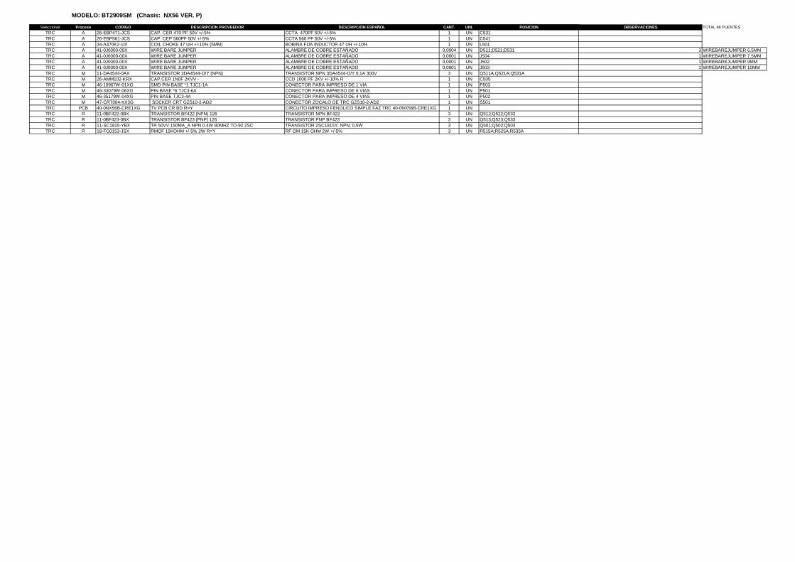
MODELO: BT2909SM (Chasis: NX56 VER. P)
Seleccionar Proceso CODIGO DESCRIPCION PROVEEDOR DESCRIPCION ESPAÑOL CANT. UNI. POSICION OBSERVACIONES TOTAL 86 PUENTES
TRC A 26-EBP471-JCS CAP. CER 470 PF 50V +/-5% CCTA 470PF 50V +/-5% 1 UN C531TRC A 26-EBP561-JCS CAP. CEP 560PF 50V +/-5% CCTA 560 PF 50V +/-5% 1 UN C541TRC A 34-A470K2-1IX COIL CHOKE 47 UH +/-10% (5MM) BOBINA FIJA INDUCTOR 47 UH +/-10% 1 UN L501TRC A 41-0J0000-00X WIRE BARE JUMPER ALAMBRE DE COBRE ESTAÑADO 0,0004 UN D511;D521;D531 3 WIREBAREJUMPER 6.5MMTRC A 41-0J0000-00X WIRE BARE JUMPER ALAMBRE DE COBRE ESTAÑADO 0,0001 UN J504 1 WIREBAREJUMPER 7.5MMTRC A 41-0J0000-00X WIRE BARE JUMPER ALAMBRE DE COBRE ESTAÑADO 0,0001 UN J502 1 WIREBAREJUMPER 9MMTRC A 41-0J0000-00X WIRE BARE JUMPER ALAMBRE DE COBRE ESTAÑADO 0,0001 UN J503 1 WIREBAREJUMPER 10MMTRC M 11-DA4544-0AX TRANSISTOR 3DA4544-O/Y (NPN) TRANSISTOR NPN 3DA4544-O/Y 0,1A 300V 3 UN Q511A;Q521A;Q531ATRC M 26-AMM102-KRX CAP.CER 1N0F 2KVV - CCD 1000 PF 2KV +/-10% R 1 UN C505TRC M 46-10967W-01XG SMD PIN BASE *1 TJC1-1A CONECTOR PARA IMPRESO DE 1 VIA 1 UN P503TRC M 46-33079W-06XG PIN BASE *6 TJC3-6A CONECTOR PARA IMPRESO DE 6 VIAS 1 UN P501TRC M 46-35179W-04XG PIN BASE TJC3-4A CONECTOR PARA IMPRESO DE 4 VIAS 1 UN P502TRC M 47-CRT004-XX3G SOCKER CRT GZS10-2-AD2 CONECTOR ZOCALO DE TRC GZS10-2-AD2 1 UN S501TRC PCB 40-0NX56B-CRE1XG TV PCB CR BD R=Y CIRCUITO IMPRESO FENOLICO SIMPLE FAZ TRC 40-0NX56B-CRE1XG 1 UNTRC R 11-0BF422-0BX TRANSISTOR BF422 (NPN) 126 TRANSISTOR NPN BF422 3 UN Q512;Q522;Q532TRC R 11-0BF423-0BX TRANSISTOR BF423 (PNP) 126 TRANSISTOR PNP BF423 3 UN Q513;Q523;Q533TRC R 11-SC1815-YBX TR 50VV 150MA_A NPN 0.4W 80MHZ TO-92 2SC TRANSISTOR 2SC1815Y; NPN; 0,5W 3 UN Q501;Q502;Q503TRC R 18-FG0153-JSX RMOF 15KOHM +/-5% 2W R=Y RF OM 15K OHM 2W +/-5% 3 UN R515A;R525A;R535A

1. General description
The UOC-TOP-64 series is a very flexible concept which offers attractive solutions for 1fH TV receivers with CRTs. This new concept offers a complete range of products with the right price level to cover TV receivers from basic mono 14 inch sets up to the best featured large and/or wide screen AV-stereo TV sets. The UOC-TOP-64 concept can also be used as front-end for 2fH and LCD TV receivers.
The UOC-TOP-64 concept is mounted in a SDIP64 package and is split up in the following ranges:
• AV-110 (AV-stereo) concept. It contains a video processor with many features and it has an analog audio control circuit with balance, treble, bass and loudness control. Two different micro processor are available for this concept, one with OSD and Closed Captioning or Teletext and Closed Captioning features (UOCTOP_1PTXT version), the other with (extended) OSD features (UOCTOP_OSD version). The block diagram is given in Figure 1.
• AV-90 concept. This concept is nearly identical to the AV-110 concept. The only difference that it does not contain an East-West and Scan Velocity Modulation (SVM) output. This concept is intended for 90× picture tubes.
• Mono-110 concept. The functional content of this concept is comparable with that of the AV 110 concept, however, it has just stereo input switch and no audio control circuit. The block diagram is given in Figure 1.
• Mono-90 concept. This concept is intended for 90× picture tubes. The circuit has an audio switch for mono signals but the mono inputs can also be used as a stereo input. In this range most of the video and audio processing features have been omitted. Also this concept can be supplied with one of the two micro processors (UOCTOP_1PTXT or UOCTOP_OSD version). The block diagram is given in Figure 2.
The most important features of the complete IC series are given in the following feature lists.
All packages are according to the ROHS legislation, which also means that these packages are lead-free. The ICs have supply voltages of 8V, 5V and 3.3V.
UOC-TOP-64 is supported by a comprehensive Global TV Software Development kit to enable easy programming and fast time-to-market (see also Section 20.4 “Licenses”).
UOC-TOP-64 N1 seriesVersatile signal processor for CRT TV applicationsRev. 0.11 — 25 January 2007 Product data sheet

<Document ID> © NXP B.V. 2007. All rights reserved.
Product data sheet Rev. 0.11 — 25 January 2007 2 of 230
NXP Semiconductors UOC-TOP-64 N1 seriesSignal processor for CRT TV
2. Features
2.1 Analog Video Processing
2.1.1 Overview of available features (AV-110/90 and Mono-110 concept)Multi-standard vision IF circuit with alignment-free PLL demodulatorInternal (switchable) time-constant for the IF-AGC circuitSwitchable group delay correction and sound trap (with switchable centre frequency) for the demodulated CVBS signalSeparate Second Sound IF output or FM demodulator output without de-emphasis available, which can be used as input for an external BTSC decoder or as input for external sound band-pass filter for second language processing.Separate SSIF input available as input for the FM-PLL demodulator to demodulate FM-radio with an IF frequency of 10.7 MHz, or as input from an external sound band-pass filter for second language processing.AM demodulator without extra reference circuitThe mono intercarrier sound circuit has a selective FM-PLL demodulator which can be switched to the different FM sound frequencies (4.5/5.5/6.0/6.5 MHz). The quality of this system is such that the external band-pass filters can be omitted. The FM-PLL demodulator can be set to centre frequencies of 4.72/5.74 MHz so that a second sound channel can be demodulated. In such an application it is necessary that an external bandpass filter is inserted. Audio switch circuit with 2 stereo inputs (1 stereo input can also be switched into two mono sound inputs) and a stereo output which can be used for the drive of for audio power amplifiers (with volume and tone-control) or as SCART/CINCH output. The second stereo input is only available via the combined C2/C3/C4/AUDIOIN5R pin for the right channel and via the combined CVBS4/Y4/AUDIOIN5L pin for the left channel.Video switch with 3 external CVBS inputs. All CVBS inputs can be used as Y-input for Y/C signals. However, only 1 Y/C source can be selected because the circuit has 1 chroma input. CVBS3/Y3 input available in combination with the G/Y-3 input pin.1 CVBS output, this output can be used as monitor video output or as front-end video output or as independent selectable video output. Automatic Y/C signal detector.Integrated luminance delay line with adjustable delay timeOnly one reference (24.576 MHz) crystal required for the m-Controller, Teletext- and the color decoder Multi-standard color decoder with automatic search system and various “forced mode” possibilitiesInternal base-band delay lineIndication of the Signal-to-Noise ratio of the incoming CVBS signalLinear RGB/YPBPR input. Scan Velocity Modulation output. The SVM circuit is active for all the incoming CVBS, Y/C and RGB/YPBPR signals. The SVM output is combined with the black current input of the black current stabilisation circuit. By means of a small application adaptation both functions can be operational in parallel.
<Document ID> © NXP B.V. 2007. All rights reserved.
Product data sheet Rev. 0.11 — 25 January 2007 3 of 230
NXP Semiconductors UOC-TOP-64 N1 seriesSignal processor for CRT TV
Picture improvement features with peaking (with switchable centre frequency, depeaking, variable positive/negative peak ratio, variable pre-/overshoot ratio and video dependent coring), dynamic skin tone control, gamma control and blue- and black stretching. All features are available for CVBS, Y/C and RGB/YPBPR signalsThe effect of the various features can de demonstrated by means of a ‘split screen’ mode in which the features are activated in one half of the picture and switched off in the other halfSwitchable DC transfer ratio for the luminance signalTint control for external RGB/YPBPR signalsContrast reduction possibility during mixed-mode of OSD and Text signals. Option to make a colored and in contrast reduced window.RGB control circuit with ‘Continuous Cathode Calibration’, white point and black level off-set adjustment so that the color temperature of the dark and the light parts of the screen can be chosen independently. When this ‘Continuous Cathode Calibration’ is not used, simple alignment of the cutoff level is possible.Adjustable ‘wide blanking’ of the RGB outputsHorizontal synchronization with two control loops and alignment-free horizontal oscillatorVertical count-down circuitVertical driver optimized for DC-coupled vertical output stagesHorizontal and vertical geometry processing with horizontal parallelogram and bow correction and horizontal and vertical zoomThe IC can be used as front-end for Progressive Scan or LCD TV receiversLow-power start-up of the horizontal drive circuit
2.1.2 Features of the AV-110/90 concept which are not available in the Mono-110 concept
Analog audio tone control circuit with treble, bass and loudness controls
2.1.3 Features of the AV-110 and Mono-110 concept which are not available in the AV-90 concept
Horizontal geometry processing and Scan Velocity Modulation output
2.1.4 Differences in feature list for the MONO-90 concept compared with AV-110/90 and Mono-110 concept
Audio switch circuit with 1 stereo input, which can also be switched into two mono sound inputs, a mono output for SCART/CINCH with the possibility to serve as front/monitor audio output.Stereo output (with volume and AVL) for audio power amplifiers. This stereo output can also be switched to one mono loudspeaker output and one fixed mono sound output.CVBS output, this output can only be used as monitor video output or as front-end video output.Only basic video processing. The remaining video features are peaking with coring, black stretching and gamma control.No horizontal geometry processing and Scan Velocity Modulation output.

<Document ID> © NXP B.V. 2007. All rights reserved.
Product data sheet Rev. 0.11 — 25 January 2007 4 of 230
NXP Semiconductors UOC-TOP-64 N1 seriesSignal processor for CRT TV
2.2 Micro-Controller80C51 m-controller core standard instruction set and timing0.9766 ms machine cyclemaximum of 80 k x 8-bit late programmed ROMmaximum of 3 k x 8-bit Auxiliary RAMI2C byte level bus interface.Interrupt controller for individual enable/disable with two level priorityTwo 16-bit Timer/Counter registersOne 24-bit Timer (16-bit timer with 8-bit Pre-scaler)16-bit Data pointerWatchDog timerAuxiliary RAM page pointerStand-by, Idle and Power Down modesUp to 13 general-purpose I/O pins14 bits PWM for Voltage Synthesis Tuning8-bit A/D converter with 4 multiplexed inputs4 PWM (6-bits) outputs for analogue control functions
2.3 Data Capture (Teletext and Closed Caption devices)Text memory for 1 pageInventory of transmitted Teletext pages stored in the Transmitted Page Table (TPT) and Subtitle Page Table (SPT)Data Capture for US Closed CaptionData Capture for 525/625 line WST, VPS (PDC system A) and 625 line Wide Screen Signalling (WSS) bit decodingAutomatic selection between 525 WST/625 WSTAutomatic selection between 625 WST/VPS on line 16 of VBIReal-time capture and decoding for WST Teletext in Hardware, to enable optimized m-processor throughputAutomatic detection of FASTEXT transmissionReal-time packet 26 engine in Hardware for processing accented, G2 and G3 charactersSignal quality detector for video and WST/VPS data typesComprehensive teletext language coverageVertical Blanking Interval (VBI) data capture of WST data
<Document ID> © NXP B.V. 2007. All rights reserved.
Product data sheet Rev. 0.11 — 25 January 2007 5 of 230
NXP Semiconductors UOC-TOP-64 N1 seriesSignal processor for CRT TV
2.4 Display
2.4.1 Features of the OSD-only devicesUp to 4 character sets with 256 characters each (size 16 pixels x 18 lines)Enhanced OSD modes 50Hz/60Hz display timing modesSerial and Parallel Display AttributesSingle/Double Width and Height for charactersScrolling of display regionVariable flash rate controlled by softwareEnhanced display features including overlining, underlining and italicsSoft colors using CLUT with 4096 color paletteGlobal selectable matrix: (12/16) By attribute selectable: 1.5x characters (18/24)Globally selectable character spacingFringing (Shadow) selectable from N-S-E-W directionFringe color selectableContrast reduction of defined area with option of colorationProgrammable CursorSpecial Graphics Characters with two planes, allowing four colors per character
2.4.2 Features of the Teletext and Closed Caption devicesFour character setsUp to 576 characters with a size of 12 pixels x 16 lines are supportedTeletext and Enhanced OSD modes50Hz/60Hz display timing modesSerial and Parallel Display AttributesScrolling of display regionVariable flash rate controlled by softwareSoft colors using CLUT with 4096 color paletteGlobal selectable matrix: (12) Features of level 1.5 WST and US Close CaptionSingle/Double/Quadruple Width and Height for characters64 software redefinable On-Screen display charactersG1 Mosaic graphics, Limited G3 Line drawing charactersWST Character sets and Closed Caption Character set in single deviceCurtaining effect via softwareFringing (Shadow) selectable from N-S-E-W directionFringe color selectableContrast reduction of defined area with option of colorationProgrammable CursorSpecial Graphics Characters with two planes, allowing four colors per character
<Document ID> © NXP B.V. 2007. All rights reserved.
Product data sheet Rev. 0.11 — 25 January 2007 6 of 230
NXP Semiconductors UOC-TOP-64 N1 seriesSignal processor for CRT TV
3. Quick reference data
[1] The supply voltage for the analogue audio part of the mono-90 version can be 5V or 8V. For a supply voltage of 5V the maximum signal amplitudes at in and outputs are 1Vrms. For a supply voltage of 8V the maximum output signal amplitude is 2 Vrms. The AV-110/90 and Mono-110 versions need a supply voltage of 8 V.
[2] The YPBPR input signal amplitudes are based on a color bar signal with 100% saturation.
Table 1: Quick reference data
SYMBOL PARAMETER MIN. TYP. MAX. UNITSupplyVP analogue supply voltage VSP 4.7 5.0 5.3 V
IP supply current (5.0 V) − 160 − mA
VDDA digital supply VSP / analogue supply periphery 3.0 3.3 3.6 V
IDDA supply current (3.3 V); Mono90 version − 50 − mA
IDDA supply current (3.3 V); AV110/90 and Mono110 versions − 70 − mA
VPAudio[1] audio supply voltage 4.7 8.0 8.4 V
IPAudio[1] supply current (5.0/8.0 V); mono-90 version − 0.5 − mA
IPAudio supply current (8.0 V); AV-110/90 and mono-110 version − 10 − mA
Ptot total power dissipation − − 1.1 W
Input voltagesViVIFrms) video IF amplifier sensitivity (RMS value) − 75 150 µV
ViSSIF(rms) sound IF amplifier sensitivity (RMS value) − 1.0 − mV
ViAUDIO(rms) external audio input (RMS value) − 1.0 1.3 V
ViCVBS(p-p) external CVBS/Y input (peak-to-peak value) − 1.0 1.4 V
ViCHROMA(p-p) external chroma input voltage (burst amplitude) (peak-to-peak value)
− 0.3 1.0 V
ViRGB(p-p) RGB inputs (peak-to-peak value) − 0.7 0.8 V
ViY(p-p) luminance input signal (peak-to-peak value) − 1.0 − V
ViPB(p-p) PB input signal (peak-to-peak value)[2] − 0.7 − V
ViPR(p-p) PR input signal (peak-to-peak value)[2] − 0.7 − V
Output signalsVo(IFVO)(p-p) demodulated CVBS output (peak-to-peak value) − 2.0 − V
Vo(QSSO)(rms) sound IF intercarrier output (RMS value) − 100 − mV
Vo(AMOUT)(rms) demodulated AM sound output (RMS value) − 250 − mV
Vo(AUDIO)(rms)[1] non-controlled audio output signals (RMS value) 1.0 − − V
Vo(CVBSO)(p-p) selected CVBS output (peak-to-peak value) − 2.0 − V
Io(AGCOUT) tuner AGC output current range 0 − 1 mA
VoRGB(p-p) RGB output signal amplitudes (peak-to-peak value) − 1.2 − V
IoHOUT horizontal output current 10 − − mA
IoVERT vertical output current (peak-to-peak value) − 1 − mA
IoEWD EW drive output current − − 1.2 mA
<Document ID> © NXP B.V. 2007. All rights reserved.
Product data sheet Rev. 0.11 — 25 January 2007 9 of 230
NXP Semiconductors UOC-TOP-64 N1 seriesSignal processor for CRT TV
5. Block diagram
**) The mono-110 version has only volume control and no tone control functions
Fig 1. Block diagram of the “AV-110/90” and “MONO-110” TV processor
V-D
RIV
E
EWD
/AV
LEHTO
AM
DEM
OD
ULA
TOR
VIS
ION
IF/A
GC/
AFC
PLL
DEM
OD
.
VID
EO A
MP.
SOU
ND
TRA
PG
ROU
P D
ELA
Y
VID
EO S
WIT
CH
VID
EO ID
ENT.
VID
EO F
ILTE
RS
DEC
OD
ERPA
L/SE
CAM
/NTS
C
BASE
-BA
ND
DEL
AY
LIN
E
H/V
SY
NC
SEP.
H-O
SC. +
PLL
2nd L
OO
PH
-SH
IFT
H-D
RIV
E
VER
TICA
L
GEO
MET
RY
& E
AST
-WES
T
AG
COU
T
VIF
IN
C2/C
3/C4
/
CVB
S4/Y
4
H-O
UT
PEA
KIN
G
SCA
N V
ELO
CITY
RG
B/Y
P RP B
CON
.
BRI
RO/G
O/B
O/
BLKIN/
RGB
CON
TRO
LO
SD/T
EXT
INSE
RT
WH
ITE-
P. A
DJ.
CON
TR/B
RIG
HTN
RGB
MAT
RIX
H/V
REF
Y D
ELA
Y A
DJ.
SKIN
TO
NE
U/V
TIN
TSA
TURA
TIO
NM
OD
ULA
TIO
N
CVB
S2/Y
2
YSY
NC
IFV
O/S
VO
/PIP
AVL/
SSIF
OU
T/FM
DEM
OU
T SOU
ND
PLL
DEE
MPH
ASI
S
R3/
G3/
B3/
YP B
P R
BLU
E/BL
AC
K-S
TRET
CH
GA
MM
A C
ON
TRO
L
BCLIN
CLK
GEN
ERA
TIO
N
I2 C-B
US
////////
//
//CSO
CSI
H/V
DIS
POH
/VD
ISPI
CLK
ICL
KO
IREF
RG
B
R/G
/B
VD
SIN
S.
CIRN
CORB
SDA
/SCL
IREF
IREF
O
CVBS
REF
CV
BS
IN
RES
ETTM
SEL
µ-PROCESSOR / TELETEXT DECODER / OSD
AM
AU
DIO
SEL
ECT
SCA
RT/
CIN
CH
LR
LS A
UD
IO O
UTP
UT
VO
LUM
E/TO
NE*
*)
SAT
CO
NTR
OL
IN
P R-3
/Y
-3
P B-3
FM
SOU
ND
-DO
WN
-M
IXER
SWIT
CH
AU
DIO
IN5R
AU
DIO
IN5L
SVM/
C2/C
3/C4
CVB
S3/
Y3
I/Os
CCC/
BLA
CK
AD
J.
LS/S
CART
/CIN
CH-O
UT
VGUARD
SEC
AM
AVL
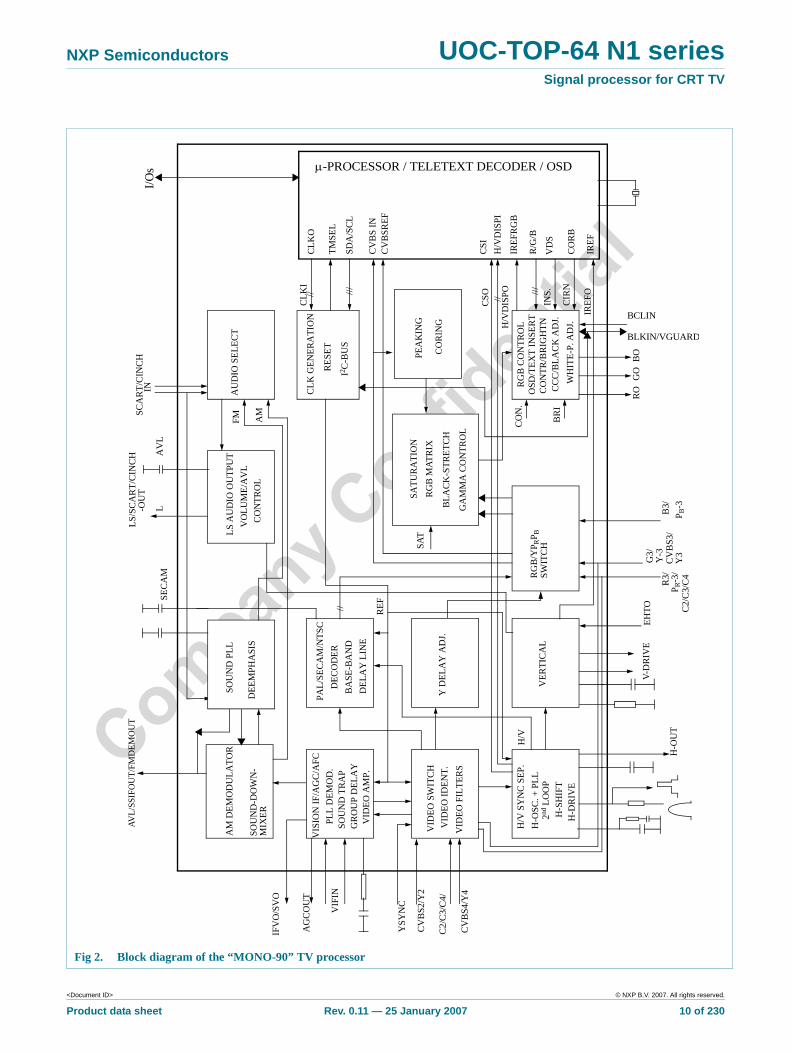
<Document ID> © NXP B.V. 2007. All rights reserved.
Product data sheet Rev. 0.11 — 25 January 2007 10 of 230
NXP Semiconductors UOC-TOP-64 N1 seriesSignal processor for CRT TV
Fig 2. Block diagram of the “MONO-90” TV processor
V-D
RIV
EEH
TO
AM
DEM
OD
ULA
TOR
VIS
ION
IF/A
GC/
AFC
PLL
DEM
OD
.
VID
EO A
MP.
SOU
ND
TRA
PG
RO
UP
DEL
AY
VID
EO S
WIT
CHV
IDEO
IDEN
T.V
IDEO
FIL
TERS
DEC
OD
ERPA
L/SE
CAM
/NTS
C
BASE
-BA
ND
DEL
AY
LIN
E
H/V
SY
NC
SEP
.H
-OSC
. + P
LL2nd
LO
OP
H-S
HIF
TH
-DRI
VE
VER
TIC
AL
AG
CO
UT
VIF
IN
H-O
UT
RGB/
YP R
P B
CON
.
BRI
ROG
OBO
BLKIN/VGUARD
RGB
CON
TRO
LO
SD/T
EXT
INSE
RT
CCC/
BLA
CK A
DJ.
WH
ITE-
P. A
DJ.
CO
NTR
/BR
IGH
TN
RGB
MAT
RIX
H/V
REF
Y D
ELA
Y A
DJ.
SATU
RATI
ON
CVBS
2/Y
2
YSY
NC
IFV
O/S
VO
SOU
ND
PLL
DEE
MPH
ASI
S
B3/BL
ACK
-STR
ETCH
BCLINC
LK G
ENER
ATI
ON
I2 C-B
US
////////
//
//CSO
CSI
H/V
DIS
POH
/VD
ISPI
CLK
IC
LKO
IREF
RGB
R/G
/B
VD
SIN
S.
CIRN
CORB
SDA
/SCL
IREF
IREF
O
CVBS
REF
CVBS
IN
RESE
TTM
SEL
µ-PROCESSOR / TELETEXT DECODER / OSD
AM
AU
DIO
SEL
ECT
SCA
RT/C
INCH
LS/S
CART
/CIN
CH
L
LS A
UD
IO O
UTP
UT
VO
LUM
E/A
VL
SAT
CO
NTR
OL
IN
P B-3
FM
SOU
ND
-DO
WN
-M
IXER
SWIT
CH
-OU
T
SECA
M
PEA
KIN
G
R3/
G3/
P R-3
/Y
-3
C2/C
3/C4
CVBS
3/Y
3
C2/
C3/
C4/
CVBS
4/Y
4
I/Os
AVL/
SSIF
OU
T/FM
DEM
OU
T
AV
L
CO
RIN
G
GA
MM
A C
ON
TRO
L

<Document ID> © NXP B.V. 2007. All rights reserved.
Product data sheet Rev. 0.11 — 25 January 2007 11 of 230
NXP Semiconductors UOC-TOP-64 N1 seriesSignal processor for CRT TV
6. Pinning information
Table 6: Pinning informationSYMBOL SDIP64 DESCRIPTION
AV-110 Mono-110
AV-90 Mono-90
IFVO/SVO/PIP [3] 1 1 − IF video output / selected CVBS output / PIP outputIFVO/SVO [3] − − 1 IF video output / selected CVBS outputVP2 2 2 2 2nd supply voltage TV processor (+5 V)VCC8V 3 3 3 8 Volt supply for audio switchesPLLIF 4 4 4 IF-PLL loop filterGND2 5 5 5 ground 2 for TV processorDECSDEM 6 6 6 decoupling sound demodulatorAVL/SSIFOUT/SNDDEMOUT[2] 7 7 7 AVL / Second sound IF output / sound demodulator outputEHTO 8 8 8 EHT/overvoltage protection inputAGCOUT 9 9 9 tuner AGC output IREF 10 10 10 reference current inputVSC 11 11 11 vertical sawtooth capacitorVIFIN2 12 12 12 IF input 2VIFIN1 13 13 13 IF input 1VDRA 14 14 14 vertical drive A outputVDRB 15 15 15 vertical drive B outputEWD/AVL 16 − − East-West drive output / AVL capacitor AVL − 16 16 AVL capacitor DECBG 17 17 17 bandgap decouplingSECPLL 18 18 18 SECAM PLL decouplingGND1 19 19 19 ground 1 for TV-processorPH1LF 20 20 20 phase-1 filterPH2LF 21 21 21 phase-2 filterVP1 22 22 22 1st supply voltage TV-processor (+5 V)DECDIG 23 23 23 decoupling digital supplyXTALOUT 24 24 24 crystal oscillator outputXTALIN 25 25 25 crystal oscillator inputP1.5 26 26 26 port 1.5P3.3/ADC3/PWM3 27 27 27 port 3.3 or ADC3 input or PWM3 outputP3.2/ADC2/PWM2 28 28 28 port 3.2 or ADC2 input or PWM2 outputP3.1/ADC1/PWM1 29 29 29 port 3.1 or ADC1 input or PWM1 output P3.0/ADC0/PWM0 30 30 30 port 3.0 or ADC0 input or PWM0 outputP2.1/PWM0 31 31 31 port 2.1 or PWM0 outputP2.0/TPWM 32 32 32 port 2.0 or Tuning PWM outputVDDP(3.3V) 33 33 33 supply to periphery (3.3V)P1.7/SDA 34 34 34 port 1.7 or I2C-bus data lineP1.6/SCL 35 35 35 port 1.6 or I2C-bus clock lineP1.3/T1 36 36 36 port 1.3 or Counter/Timer 1 inputP1.1/T0 37 37 37 port 1.1 or Counter/Timer 0 inputP1.0/INT1 38 38 38 port 1.0 or external interrupt 1INT0/P0.5 39 39 39 external interrupt 0 or port 0.5 (4 mA current sinking capability for
direct drive of LEDs)VDDC(3.3V) 40 40 40 supply
<Document ID> © NXP B.V. 2007. All rights reserved.
Product data sheet Rev. 0.11 — 25 January 2007 12 of 230
NXP Semiconductors UOC-TOP-64 N1 seriesSignal processor for CRT TV
[1] The function of these pins is dependent on some I2C-bus control bits. More details are given in Table 7.
[2] The function of this pin is selected by means of the CMB2-0 bits
[3] The function of this pin is selected by means of the SVO1-0 bits
[4] The SSIF input is selected by means of the SSIFM bit
[5] The choice between two mono inputs or one stereo input is realized by means of the bits SAS3-0
[6] The black current input, vertical guard input and SVM output (AV-110/90 and Mono-110 versions) have been combined on this pin. For a reliable operation of the protection system and the black current stabilization system or SVM system, the end of the vertical guard protection pulse during normal operation should not overlap the measuring pulses. Therefore this pulse must end before line 14.
GND5 41 41 41 groundVPE 42 42 42 OTP Programming VoltageVDDA1(3.3V) 43 43 43 supply voltageBO/PBOUT 44 44 − Blue output / PB outputBO − − 44 Blue outputGO/YOUT 45 45 − Green output / Y outputGO − − 45 Green outputRO/PROUT 46 46 − Red output / PR outputRO − − 46 Red outputBLKIN/VGUARD/SVM [1][6] 47 − − black current input / vertical guard / scan velocity modulation
outputBLKIN/VGUARD [1][6] − 47 47 black current input / vertical guardBCLIN 48 48 48 beam current limiter inputB3/PB3 49 49 49 3rd B input / PB inputG3/Y3/CVBS3/Y3 [1] 50 50 50 3rd G input / Y input / CVBS input / Y inputR3/PR3/C2/C3/C4 [1] 51 51 51 3rd R input / PR input / C2/3/4 inputYOUT 52 52 52 Y-output (for YUV interface)YSYNC 53 53 53 Y-input for sync separatorVP3 54 54 54 supply voltage (5 V)GND3 55 55 55 ground connectionHOUT 56 56 56 horizontal outputFBISO/SANDCA 57 57 57 flyback input/sandcastle outputAUDOUTSM2/LSR 58 58 58 audio output for audio power amplifier (right signal) or fixed audio
output for mono applicationsAUDOUTLSM1/LSL 59 59 59 audio output for audio power amplifier (left signal) or speaker
output for mono applicationsC2/C3/C4/AUDIOIN5R [1] 60 60 - chroma-2/3/4 input / audio 5 right inputC2/C3/C4 − − 60 chroma-2/3/4 inputAUDIOIN3/IN1R [5] 61 61 61 audio 3 input / right stereo inputCVBS2/Y2 62 62 62 CVBS2/Y2 inputAUDIOIN2/IN1L/SSIF [4][5] 63 63 63 audio 2 input / left stereo input / sound IF inputCVBS4/Y4/AUDIOIN5L [1] 64 64 − CVBS4/Y4 input / audio 5 left inputCVBS4/Y4 − − 64 CVBS4/Y4 input
Table 6: Pinning informationSYMBOL SDIP64 DESCRIPTION
AV-110 Mono-110
AV-90 Mono-90

PRODUCT PREVIEW
® STV8172AVertical Deflection Booster
for 3-APPTV/Monitor Applications with 75-V Flyback Generator
Main Features
■ Power Amplifier
■ Flyback Generator
■ Stand-by Control
■ Output Current up to 3 App
■ Thermal Protection
Description
The STV8172A is a vertical deflection booster designed for TV and monitor applications.
This device, supplied with up to 35 V, provides up to 2.5 App output current to drive the vertical deflection yoke.
The internal flyback generator delivers flyback voltages up to 75 V.
In double-supply applications, a stand-by state will be reached by stopping the (+) supply alone.
HEPTAWATT(Plastic Package)
ORDER CODE: STV8172A
7654321
Tab connected
Input (Non Inverting)Output Stage SupplyOutputGround Or Negative SupplyFlyback GeneratorSupply VoltageInput (Inverting)
to pin 4
1Thermal
Protection
6
4
3
5
STV8172A
+
-Power
Amplifier
7
2
FlybackGenerator
Inverting
Non-Inverting
Input
Input
Ground or Negative Supply
Output
FlybackGenerator
Output Stage SupplyVoltageSupply
This is preliminary information on a new product now in development. Details are subject to change without notice.
August 2003 Revision 1.0 ADCS No. 7564264 STMicroelectronics Confidential 1/14
Absolute Maximum Ratings STV8172A
1 Absolute Maximum Ratings
Note:1. Usually the flyback voltage is slightly more than 2 x VS. This must be taken into consideration when setting VS.
2. Versus pin 4
3. V3 is higher than VS during the first half of the flyback pulse.
4. Such repetitive output peak currents are usually observed just before and after the flyback pulse.
5. This non-repetitive output peak current can be observed, for example, during the Switch-On/Switch-Off phases. This peak current is acceptable providing the SOA is respected (Figure 8 and Figure 9).
6. All pins have a reverse diode towards pin 4, these diodes should never be forward-biased.
7. Input voltages must not exceed the lower value of either VS + 2 or 40 volts.
2 Thermal Data
Symbol Parameter Value Unit
Voltage
VS Supply Voltage (pin 2) - Note 1 and Note 2 40 V
V5, V6 Flyback Peak Voltage - Note 2 70 V
V3 Voltage at Pin 3 - Note 2, Note 3 and Note 6 -0.4 to (VS + 3) V
V1, V7 Amplifier Input Voltage - Note 2, Note 6 and Note 7 - 0.4 to (VS + 2) or +40 V
Current
I0 (1) Output Peak Current at f = 50 to 200 Hz, t � 10µs - Note 4 ±5 A
I0 (2) Output Peak Current non-repetitive - Note 5 ±2 A
I3 Sink Sink Current, t<1ms - Note 3 2 A
I3 Source Source Current, t � 1ms 2 A
I3 Flyback pulse current at f=50 to 200 Hz, t�10�s - Note 4 ±5 A
ESD Susceptibility
ESD1 Human body model (100 pF discharged through 1.5 k�) 2 kV
ESD2 EIAJ Standard (200 pF discharged through 0 �) 300 V
Temperature
Ts Storage Temperature -40 to 150 °C
Tj Junction Temperature +150 °C
Symbol Parameter Value Unit
RthJC Junction-to-Case Thermal Resistance 3 °C/W
TT Temperature for Thermal Shutdown 150 °C
TJ Recommended Max. Junction Temperature 120 °C
2/14 STMicroelectronics Confidential
STV8172A Electrical Characteristics
3 Electrical Characteristics
(VS = 34 V, TAMB = 25°C, unless otherwise specified)
8. In normal applications, the peak flyback voltage is slightly greater than 2 x (VS - V4). Therefore, (VS - V4) = 35 V is not allowed without special circuitry.
9. Refer to Figure 4, Stand-by condition.
Symbol Parameter Test Conditions Min. Typ. Max. Unit Fig.
Supply
VS Operating Supply Voltage Range (V2-V4) Note 8 10 35 V
I2 Pin 2 Quiescent Current I3 = 0, I5 = 0 5 20 mA 1
I6 Pin 6 Quiescent Current I3 = 0, I5 = 0, V6 =35v 8 19 50 mA 1
Input
I1 Input Bias Current V1 = 1 V, V7 = 2.2 V - 0.6 -1.5 µA 1
I7 Input Bias Current V1 = 2.2 V, V7 = 1 V - 0.6 -1.5 µA
VIR Operating Input Voltage Range 0 VS - 2 V
VI0 Offset Voltage 2 mV
�VI0/dt Offset Drift versus Temperature 10 µV/°C
Output
I0 Operating Peak Output Current 0o<Tcase<125oC �1.5 A
V5L Output Saturation Voltage to pin 4 I5 = 1.5 A 1 1.7 V 3
V5H Output Saturation Voltage to pin 6 I5 = -1.5 A 1.8 2.3 V 2
Stand-by
V5STBY Output Voltage in Stand-byV1 = V7 = VS = 0 See Note 9
VS - 2 V
Miscellaneous
G Voltage Gain 80 dB
VD5-6 Diode Forward Voltage Between pins 5-6 I5 = 1.5 A 1.8 2.3 V
VD3-2 Diode Forward Voltage between pins 3-2 I3 = 1.5 A 1.6 2.2 V
V3SL Saturation Voltage on pin 3 I3 = 20 mA 0.4 1 V 3
V3SH Saturation Voltage to pin 2 (2nd part of flyback) I3 = -1.5 A 2.1 2.8 V
STMicroelectronics Confidential 3/14
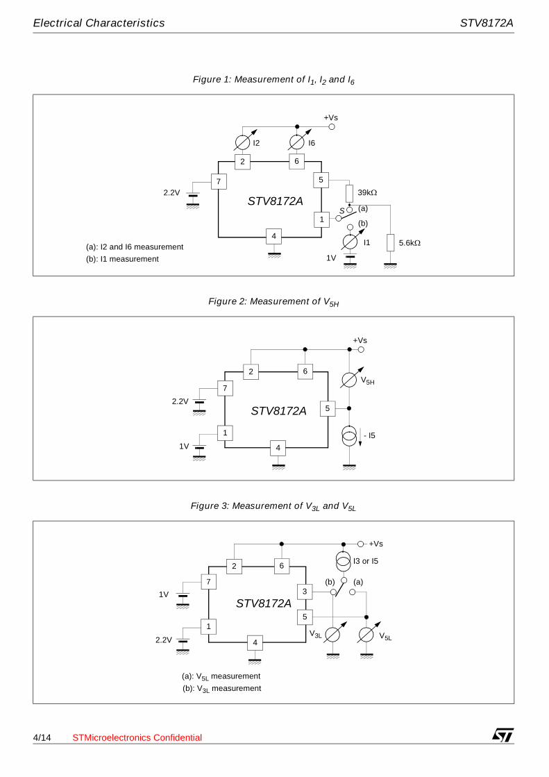
Electrical Characteristics STV8172A
Figure 1: Measurement of I1, I2 and I6
Figure 2: Measurement of V5H
Figure 3: Measurement of V3L and V5L
1V
(a)
39k�
5
1 (b)
I1(a): I2 and I6 measurement
(b): I1 measurement
S
+Vs
2 6
I2 I6
4
72.2V
STV8172A
5.6k�
- I5
5
1V
7
2.2V
1
4
+Vs
2 6V5H
STV8172A
+Vs
I3 or I5
3
5
V5LV3L
(a)(b)
(a): V5L measurement
(b): V3L measurement
STV8172A1V
7
4
2 6
2.2V
1
4/14 STMicroelectronics Confidential
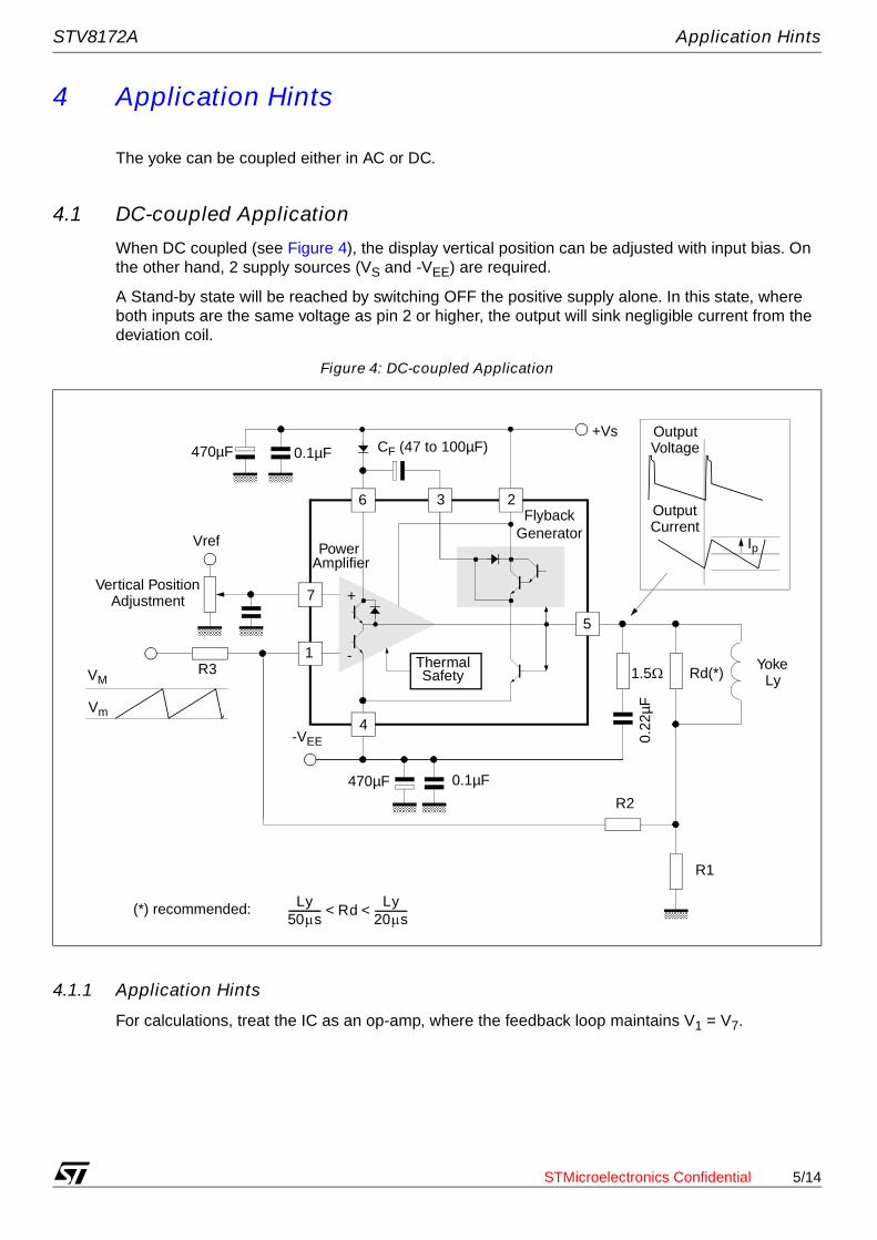
STV8172A Application Hints
4 Application Hints
The yoke can be coupled either in AC or DC.
4.1 DC-coupled Application
When DC coupled (see Figure 4), the display vertical position can be adjusted with input bias. On the other hand, 2 supply sources (VS and -VEE) are required.
A Stand-by state will be reached by switching OFF the positive supply alone. In this state, where both inputs are the same voltage as pin 2 or higher, the output will sink negligible current from the deviation coil.
4.1.1 Application Hints
For calculations, treat the IC as an op-amp, where the feedback loop maintains V1 = V7.
Figure 4: DC-coupled Application
R3
+Vs
R2
R1
Rd(*)Yoke
Ly
Vertical PositionAdjustment
-VEE
Vref
(*) recommended: Ly50�s------------- Rd
Ly20�s-------------<<
0.1µF
0.1µF
CF (47 to 100µF)
PowerAmplifier
FlybackGenerator
ThermalSafety
470µF
470µF
OutputCurrent
OutputVoltage
Ip
7
3 2
5
6
1
4
VM
Vm
+
-0.
22µF
1.5�
STMicroelectronics Confidential 5/14

Application Hints STV8172A
4.1.1.1 Centering
Display will be centered (null mean current in yoke) when voltage on pin 7 is (R1 is negligible):
4.1.1.2 Peak Current
Example: for Vm = 2 V, VM = 5 V and IP = 1 A
Choose R1 in the1 � range, for instance R1=1 �
From equation of peak current:
Then choose R2 or R3. For instance, if R2 = 10 k�, then R3 = 15 k�
Finally, the bias voltage on pin 7 should be:
4.1.2 Ripple Rejection
When both ramp signal and bias are provided by the same driver IC, you can gain natural rejection of any ripple caused by a voltage drop in the ground (see Figure 5), if you manage to apply the same fraction of ripple voltage to both booster inputs. For that purpose, arrange an intermediate point in the bias resistor bridge, such that (R8 / R7) = (R3 / R2), and connect the bias filtering capacitor between the intermediate point and the local driver ground. Of course, R7 should be connected to the booster reference point, which is the ground side of R1.
Figure 5: Ripple Rejection
V7
VM Vm+
2------------------------
R2R2 R3+----------------------� �� �� �
=
IP
VM Vm– �
2-----------------------------
R2R1xR3-------------------=
R2R3-------
2 IP R1
VM Vm–-----------------------------
23---==
V7
VM Vm+
2------------------------
1
1R3R2-------+
-----------------72----
12.5-------- 1.4V===
R3
R2 R1
Rd YokeLy
PowerAmplifier
FlybackGenerator
ThermalSafety
7
3 2
5
6
1
4
+
-
R7R8R9
ReferenceVoltage
RampSignal
DriverGround Source of Ripple
6/14 STMicroelectronics Confidential
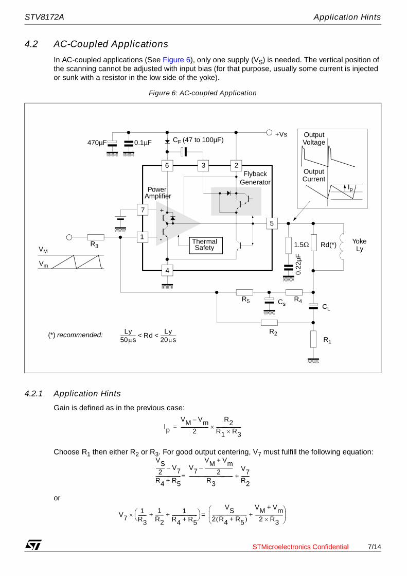
STV8172A Application Hints
4.2 AC-Coupled Applications
In AC-coupled applications (See Figure 6), only one supply (VS) is needed. The vertical position of the scanning cannot be adjusted with input bias (for that purpose, usually some current is injected or sunk with a resistor in the low side of the yoke).
4.2.1 Application Hints
Gain is defined as in the previous case:
Choose R1 then either R2 or R3. For good output centering, V7 must fulfill the following equation:
or
Figure 6: AC-coupled Application
R3
+Vs
R2R1
Rd(*) YokeLy
(*) recommended: Ly50�s------------- Rd
Ly20�s-------------<<
0.1µF CF (47 to 100µF)
PowerAmplifier
FlybackGenerator
ThermalSafety
470µF
OutputCurrent
OutputVoltage
Ip
7
3 2
5
6
1
4
VM
Vm
+
-
CsR4
CL
R50.
22µF
1.5�
IpVM Vm–
2------------------------
R2R1 R3----------------------=
VS2
-------- V7–
R4 R5+----------------------
V7
VM Vm+
2------------------------–
R3--------------------------------------
V7R2-------+=
V71
R3-------�� 1
R2-------+ 1
R4 R5+----------------------�
�VS
2 R4 R5+ �------------------------------
VM Vm+
2 R3------------------------+
� �� �� �
=+
STMicroelectronics Confidential 7/14
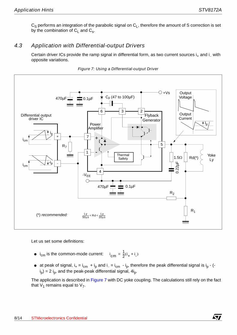
Application Hints STV8172A
CS performs an integration of the parabolic signal on CL, therefore the amount of S correction is set by the combination of CL and Cs.
4.3 Application with Differential-output Drivers
Certain driver ICs provide the ramp signal in differential form, as two current sources i+ and i� with
opposite variations.
Let us set some definitions:
● icm is the common-mode current:
● at peak of signal, i+ = icm + ip and i�
= icm - ip, therefore the peak differential signal is ip - (-ip) = 2 ip, and the peak-peak differential signal, 4ip.
The application is described in Figure 7 with DC yoke coupling. The calculations still rely on the fact that V1 remains equal to V7.
Figure 7: Using a Differential-output Driver
+Vs
R2
R1
Rd(*)Yoke
Ly
-VEE0.
22µF
(*) recommended: Ly50�s-------------- Rd
Ly20�s--------------<<
0.1µF
0.1µF
CF (47 to 100µF)
PowerAmplifier
FlybackGenerator
ThermalSafety
+
-
470µF
470µF
OutputCurrent
OutputVoltage
Ip
7
3 2
5
6
1
4
R7
+
-
Differential outputdriver IC
ip
icm
-ipicm
1.5�
icm12--- i+ i-+ �=
8/14 STMicroelectronics Confidential