manual de service fcp-7101 - fx-7102
TRANSCRIPT

8/13/2019 Manual de Service Fcp-7101 - Fx-7102
http://slidepdf.com/reader/full/manual-de-service-fcp-7101-fx-7102 1/170
F F C C P P --7 7 110011 / / F F X X --7 7 110022
Service Manual
F C P - 7 1 0 1
M a i n
P o w e r
C h a r g e
M O D E
P O W E R
O F F : H O L D 2 s e c .
L E A D
1 m V
R E S E T
S E N S E
S T A R T / S T O
P
I D
E N T E R
C A N C E L
O N / O
F F
( s t b y )
CONTRAST
・ Before setting up/maintenance, please read this service manual carefully.
・ Keep this manual where it can be always referred to.
8/13/2019 Manual de Service Fcp-7101 - Fx-7102
http://slidepdf.com/reader/full/manual-de-service-fcp-7101-fx-7102 2/170
Copyright © 2004 by Fukuda Denshi Co. Ltd.
No part of this document may be copied or transmitted in any form without the prior written
permission of Fukuda Denshi Co. Ltd.
Printed in Japan
8/13/2019 Manual de Service Fcp-7101 - Fx-7102
http://slidepdf.com/reader/full/manual-de-service-fcp-7101-fx-7102 3/170
i
Notice
This manual contains technical information on the FCP-7101/FX-7102 aimed
at Fukuda Denshi service representatives and professional engineers.Before performing maintenance the unit, read the manual carefully and use it
to help you work correctly and safely.
When you have finished using the manual, store it carefully in a designated
location.
Strictly follow the instructions of this manual whenever you perform
maintenance or make adjustments to the unit. Failure to do so may lead to a
serious accident.
Safety
This manual utilizes the graphic symbols shown below. Make sure that you
understand the meaning represented by these symbols, carefully read the
instructions given in the text, and work safely.
DANGER Failure to follow this message may result in death or serious injury to thepatient or operator, damage to the equipment, or create a fire hazard.
WARNING Failure to follow this message may result in death or serious injury to thepatient or operator.
CAUTION Failure to follow this message may cause injury to the patient, or maycause damage to the equipment.
Symbol Description
NOTE A note is not related to product safety. A note provides
information about the proper use and operating method
to prevent incorrect operation and trouble with the
unit.
Indicates an action that must not be performed.
Indicates an action that must be performed.
REFERENCE Indicates the reference page for the operation method.
8/13/2019 Manual de Service Fcp-7101 - Fx-7102
http://slidepdf.com/reader/full/manual-de-service-fcp-7101-fx-7102 4/170
ii
Servicing Precautions
In servicing the FCP-7101/FX-7102, observe the following.
DANGER Never remodel the medical electronic equipment.If remodelled, the equipment may not ensure safe operation,thereby causing accidental hazards to the patient andoperator.
CAUTION The service manual is intended for the service engineers
of Fukuda representatives and the technical staffconcerned with medical electronic equipment. Servicing,
reassembling, and adjustment shall be performed byautorized service engineers. Prepare proper facilities and tools when servicing. Be sure to follow the instructions of operation manual
when operating the instrument. For operating precautions,refer to the operation manual.
8/13/2019 Manual de Service Fcp-7101 - Fx-7102
http://slidepdf.com/reader/full/manual-de-service-fcp-7101-fx-7102 5/170
iii
CAUTION Disassembling/Reassembling Precautions
Be sure to turn the power off and disconnect the power supply cordfrom the wall outlet. Then start disassembling the instrument.
When removing the main PC board, remove the battery in advance. Take care not to disconnect and connect the key panel and sensor
board from/to the connector too frequently. Too frequent disconnectionand connection of these units may cause poor contact.
Use proper screwdrivers to loosen screws. When reassembling, make sure all screws are tightened to original
positions and all disconnected connectors are reconnected properly.
PC Board Handling Precautions PC boards are equipped with extremely sensitive devices to static
electricity. PC boards are sensitive electronic assemblies. Take proper measures
for removed PC boards, e.g. put them in a conductive bag. Handle PC boards carefully. Giving an impact to them may damage
devices mounted onto them. Never remove a PC board or connect the connector to it when it is
supplied with power.
CAUTION If you find a value which exceeds the allowable level, be sure to let theuser avoid using the instrument. If the user operates the instrument as itis, he/she may receive an hazardous accident.
Equipment Classification
The FCP-7101/FX-7102 is classified into the following equipment:
1. Protection against electrical shock
Class Ⅱ, Internally powered
2. Type against electrical shock
Applied part: Type CF
3. Degree of protection against harmful water invasion
Ordinary equipment
4. Degree of safety in using under air-inflammable anesthetic gases or
oxygen/nitrous
oxide-anesthetic gasesEquipment used under an environment containing no inflammable
anesthetic gases or no inflammable cleaning agent.
5. Running mode
Continuous running mode
8/13/2019 Manual de Service Fcp-7101 - Fx-7102
http://slidepdf.com/reader/full/manual-de-service-fcp-7101-fx-7102 6/170
iv
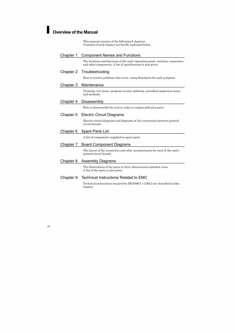
Overview of the Manual
This manual consists of the following 9 chapters.Contents of each chapter are briefly explained below.
Chapter 1 Component Names and Functions
The locations and functions of the unit's operation panel, switches, connectors,
and other components. A list of specifications is also given.
Chapter 2 Troubleshooting
How to resolve problems that occur, using flowcharts for each symptom.
Chapter 3 Maintenance
Cleaning, test menu, program version updating, periodical inspection items,
and methods.
Chapter 4 Disassembly
How to disassemble the unit in order to replace defective parts.
Chapter 5 Electric Circuit Diagrams
Electric circuit diagrams and diagrams of the connections between printed
circuit boards.
Chapter 6 Spare Parts List
A list of components supplied as spare parts.
Chapter 7 Board Component Diagrams
The layout of the connectors and other mounted parts for each of the unit's
printed circuit boards.
Chapter 8 Assembly Diagrams
The illustrations of the parts in three dimensional exploded views.
A list of the parts is also given.
Chapter 9 Technical Instructions Related to EMC
Technical instructions required by IEC60601-1-2 Ed.2 are described in this
chapter.
8/13/2019 Manual de Service Fcp-7101 - Fx-7102
http://slidepdf.com/reader/full/manual-de-service-fcp-7101-fx-7102 7/170
v
Contents
Notice ···································································································································· Safety······················································································································ ⅰ Servicing Precautions ······················································· ······································ⅱ
Equipment Classification·························································································ⅲ
Overview of the Manual ····································································································
Chapter 1 Component Names and Functions ······························································· 1-1
Unit (top face) ··················································································································· 1-1
Unit (side, rear, and bottom faces) ················································································· 1-2
Operation panel ················································································································ 1-3
Specifications list············································································································· 1-5
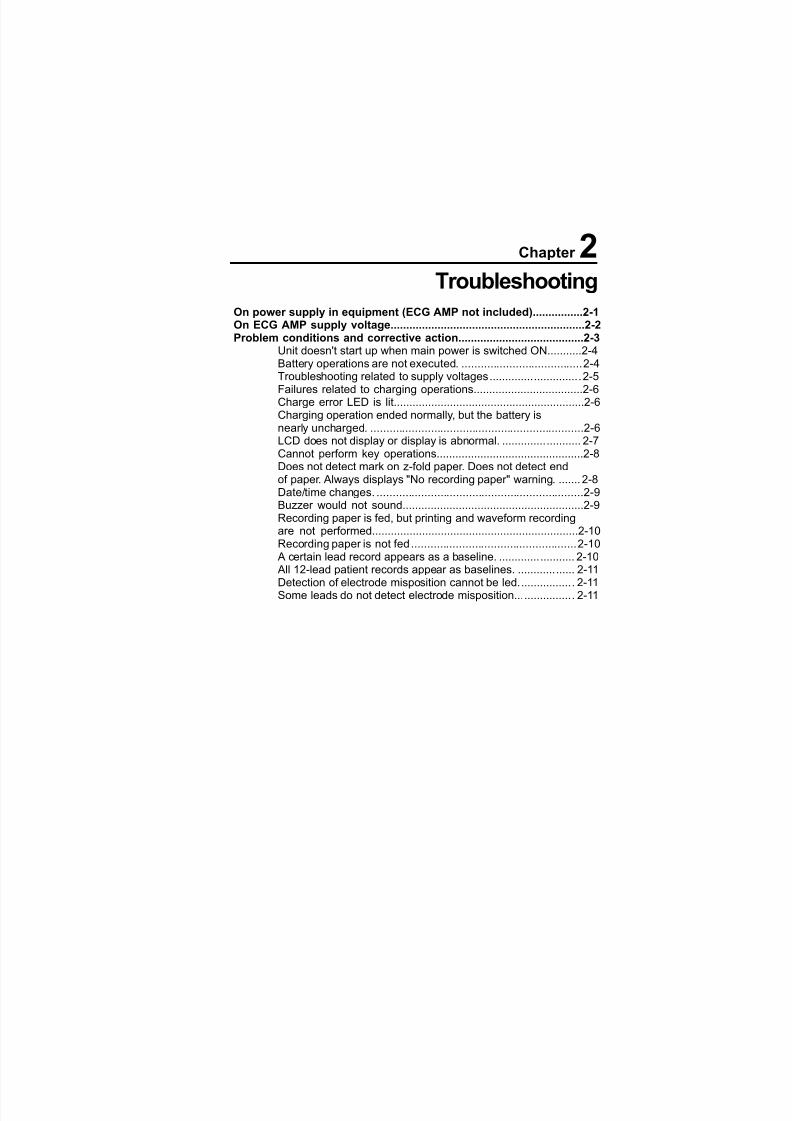
Chapter 2 Troubleshooting ····························································································· 2-1
On power supply in equipment (ECG AMP not included)········································ 2‐1
On ECG AMP supply voltage ························································ ·························· 2‐2
Problem conditions and corrective action·················· ·············································· 2‐3
Unit doesn't start up when main power is switched ON.·········································· 2‐4
Battery operations are not executed. ·············································· ························ 2‐4
Troubleshooting related to supply voltages··············································· ·············· 2‐5
Failures related to charging operations ···················································· ··············· 2‐6
Charge error LED is lit··················· ························································ ·················· 2‐6
Charging operation ended normally, but the battery is
nearly uncharged. ···················································· ··············································· 2‐6
LCD does not display or display is abnormal. ····················································· ···· 2‐7
Cannot perform key operations. ··························································· ··················· 2‐8
Does not detect mark on z-fold paper. Does not detect end
of paper. Always displays "No recording paper" warning. ······································· 2‐8
Date/time changes. ··················································· ·············································· 2‐9
Buzzer would not sound···················································· ······································ 2‐9
Recording paper is fed, but printing and waveform recording
are not performed.············································ ······················································· 2‐10
Recording paper is not fed ······················································· ······························· 2‐10
A certain lead record appears as a baseline. ························································· · 2‐10
All 12-lead patient records appear as baselines.·················································· ··· 2‐11
Detection of electrode misposition cannot be led. ··················································· 2‐11
Some leads do not detect electrode misposition. ···················································· 2‐11
Chapter 3 Maintenance···································································································· 3-1
Cleaning ···························································································································· 3‐1Cleaning the unit ··············································· ····················································· · 3
‐1Replacing the battery······································································································· 3‐2
Update of the software····································································································· 3‐4Self-diagnostics test ········································································································ 3‐5
User self-diagnostics test ··························································· ····························· 3‐6
ECG Test Pattern ··················································· ··········································· 3‐7
Recording Test ···················································· ·············································· 3‐8
Key Test ··················································· ····················································· ···· 3‐9
LCD Test ··················································· ···················································· ···· 3‐10
Buzzer Test ················································ ···················································· ··· 3‐11
Manufacturer self-diagnostics test········································ ··································· 3‐12
Status Test ················································ ····················································· ··· 3‐14
ECG A/D DATA ·························································· ······································· 3‐15
LAN Test ··················································· ···················································· ···· 3‐16Memory Test······················································ ················································ 3‐17
ROM WRITE Test························································· ····································· 3‐18
Recorder Test··················· ···················································· ····························· 3‐19
8/13/2019 Manual de Service Fcp-7101 - Fx-7102
http://slidepdf.com/reader/full/manual-de-service-fcp-7101-fx-7102 8/170
vi
Memory initialize ························································ ········································ 3‐21
UPDATE········································································· ···································· 3‐22
Periodical inspections······································································································ 3-23Periodical inspection intervals and precautions ···················································· ···3-23List of periodical inspection items ······················································· ·····················3-23Safety inspections (4 items)·····················································································3-24
Before checking the leakage current··································································3-24Checking the enclosure leakage current(current that flows from the enclosure tothe earth terminal of the power outlet)······························································3-25
Checking the patient leakage current I·······························································3-25Checking the patient leakage current III·····························································3-25Checking the patient measurement current························································3-25
Inspection of electrical performance/characteristics ················································ 3-26Hardware inspections (10 items) ·················································· ···························3-28
Periodical inspection (2) record ······················································································3-30
Chapter 4 Disassembly ···································································································· 4-1
Removing the LCD············································································································4‐1Removing the enclosure cover························································································4‐2Removing the recorder unit ····························································································· 4‐3Removing the main board ································································································ 4‐4
Chapter 5 Electric Circuit Diagrams··············································································· 5-1
Overall block diagram of unit (AC adapter not included) ·············································· 5‐1MAIN BOARD block diagram ····················································· ·····························5‐3
MAIN BOARD (PCB-6950) circuit ····················································· ······················5‐5
1.Digital logic block ······················································ ············································ 5‐5
CPU section·········································································································5‐5
FPGA section·······································································································5‐5
Memory section ······················································ ············································· 5‐6
KEY I/F section······················································ ·············································· 5‐8
Thermal head control section···············································································5‐9
Real time clock ·················································· ·················································· 5‐10
Reset circuit section·····························································································5‐11
Sensor control section ·················································· ······································· 5‐12
Motor control section····························································································5‐13
LCD voltage generating section···········································································5‐14
2.ECG AMP block····································································································5‐15
3.Power supply block·······························································································5‐16
Power voltage generating section········································································5‐17
Battery charging section ···················································· ··································5‐20
Power control section···························································································5‐21
KEY BOARD (PCB-6949) circuit··············································································5‐22
SENSOR BOARD (PCB-6948) circuit······································································5‐23
MAG UP BOARD (PCB-6951) circuit·······································································5‐23AC adaptor block diagram ·······························································································5‐24
MAIN BOARD Circuit Diagrams (PCB-6950)···································································5‐25
Power connection table No.1············································· ······································ 5‐25
Power connection table No.2············································· ······································ 5‐26
POWER /CAPACITOR/RESET IC/CLOCK
LCD POWER block··································································································5‐27
CPU block················································································································5‐28
FPGA block··············································································································5‐29
MEMORY block ············································· ···················································· ······5‐30
LAN CONTROL block······························································································5‐31
LCD I/F / RTC / LED block·······················································································5‐32
THERMAL I/F block ······················································ ··········································· 5‐33
SENSOR I/F /MAGAZIN UP SENSOR I/FMOTOR I/F /JTAG I/F block·····················································································5‐34
ECG AMP block
(Differential amplification, multiplexer section)·························································5‐35
ECG AMP block (ADC,CPLD and POWER section)················································ 5‐36
8/13/2019 Manual de Service Fcp-7101 - Fx-7102
http://slidepdf.com/reader/full/manual-de-service-fcp-7101-fx-7102 9/170
vii
MAIN POWER SUPPLY +24V block································································ ······· 5‐37
CHARGE block ················································· ···················································· ·· 5‐38
+5V /+3.3V /+1.8V Power generation block ························································ ···· 5‐39
POWER STATUS block ···················································· ······································ 5‐40
POWER / CHARGE ERROR block ················································· ························ 5‐41
+3.3VSTB / POWER ON RESET block··································································· 5‐42
BATTERY ON CONTROL / THERMAL POWER
GENERATION BLOCK ···················································· ······································· 5‐43
POWER-MAIN I / F block·················································· ······································ 5‐44
POWER ON / OFF CONTROL block ······················································ ················ 5‐45
KEY BOARD (PCB-6949)·································································································· 5‐46
SENSOR BOARD (PCB-6948) ·························································································· 5‐47
MAG UP BOARD (PCB-6951)··························································································· 5‐48
Chapter 6 Spare Parts List ······························································································ 6-1
MAIN BOARD (PCB-6950)································································································ 6‐1KEY BOARD (PCB-6949)·································································································· 6‐8SENSOR BOARD (PCB-6948) ·························································································· 6‐9MAG UP BOARD (PCB-6951)··························································································· 6‐10
Other spare parts list ······································································································ 6‐11
Chapter 7 Board Component Diagram··········································································· 7-1
MAIN BOARD (PCB-6950 component side)···································································· 7‐1MAIN BOARD (PCB-6950 soldering side)······································································· 7‐2KEY BOARD (PCB-6949 component side) ····································································· 7‐3KEY BOARD (PCB-6949 soldering side)········································································· 7‐4SENSOR BOARD (PCB-6948 component side)······························································ 7‐5MAG UP BOARD (PCB-6951 component side) ······························································ 7‐6
Chapter 8 Assembly Diagrams ······················································································· 8-1
Magazine ··························································································································· 8‐1Paper shaft························································································································ 8‐2Recorder···························································································································· 8‐3Upper case (FCP-7101) ···································································································· 8‐4Upper case (FX-7102)······································································································· 8‐5Lower case ······················································································································ 8‐6General assembly diagram (FCP-7101) ·········································································· 8‐7General assembly diagram (FX-7102)············································································· 8‐8Outline view (FCP-7101)··································································································· 8‐9Outline view (FX-7102) ····································································································· 8‐10
Paper guide······················································································································· 8‐11
50mm Magazine adapter (option)···················································································· 8‐12
50mm Paper adapter (option)·························································································· 8‐13
Chapter 9 Technical Instructions Related to EMC························································ 9-1Emission information CISPR11······················································································· 9‐2Immunity information (to other than radiation/conduction) ········································· 9‐3Immunity information (to radiation/conduction)···························································· 9‐4Recommended distance of separation from
portable telephone, etc ···································································································· 9‐5

8/13/2019 Manual de Service Fcp-7101 - Fx-7102
http://slidepdf.com/reader/full/manual-de-service-fcp-7101-fx-7102 10/170
viii
8/13/2019 Manual de Service Fcp-7101 - Fx-7102
http://slidepdf.com/reader/full/manual-de-service-fcp-7101-fx-7102 11/170

8/13/2019 Manual de Service Fcp-7101 - Fx-7102
http://slidepdf.com/reader/full/manual-de-service-fcp-7101-fx-7102 12/170
8/13/2019 Manual de Service Fcp-7101 - Fx-7102
http://slidepdf.com/reader/full/manual-de-service-fcp-7101-fx-7102 13/170
Chapter 1 Component Names and Functions
1 - 1
Unit (top face)
Liquid crystal display, operation panel, and paper magazine are provided on
the top face of the unit.
F C P - 7 1
0 1 M a
i n
P o w e
r C h a
r g e
M O D
E
P O W E R
O F F : H
O L D 2
s e c .
L E A D
1 m V
R E S E T
S E N S E
S T A
R T / S T O P
I D
E N T E R
C A N C E L
O N / O
F F
( s t b y
)
(2) Operation panel
(4) Paper magazine
(3) Magazine open button(5) Thermal print head
(1) Liquid crystal display(LCD)
(1) Liquid crystal display (LCD)Displays electrocardiogram (ECG) waveforms, patient data, unit status, etc.
(2) Operation panel
Push the key switches on the panel to operate the electrocardiograph.
Provided with the LED that indicates the operation status.
(3) Magazine open button
Push to open the magazine cover.
(4) Paper magazine
Load the recording paper here.
(5) Thermal print head
Records (prints) ECG waveforms and measured values.

8/13/2019 Manual de Service Fcp-7101 - Fx-7102
http://slidepdf.com/reader/full/manual-de-service-fcp-7101-fx-7102 14/170
Chapter 1
1 - 2
Unit (side, rear, and bottom faces)
PATIENT connector and CONTRAST volume are provided on the side of
the unit.AC adapter jack, LAN port, and potential equalization terminal are
provided on the rear face of the unit.
BATTERY PACK compartment is located on the underside of the unit.
(6) PATIENT connector
Plug in the patient cable here.
(7) CONTRAST volume
Use the volume to adjust the contrast of the LCD.
(8) AC adapter jack
Plug in the DC plug here.
(9) LAN port
Plug in the LAN cable here to communicate with a PC.
(10) Potential equalization terminal
Plug in the ground cable here.
(11) BATTERY PACK compartment
Install the optional battery pack (8PH-4/3A3700-H-J18) in this
compartment.
(11) BATTERY PACK compartment
(9) LAN port
(6) PATIENT connector
(7) CONTRAST volume
(8) AC adapter jack
(10) Potential equalization
terminal
C O N T R A S T
L A M D C I N 1 8 V
N i - M H
B A T T E R Y P A C K

8/13/2019 Manual de Service Fcp-7101 - Fx-7102
http://slidepdf.com/reader/full/manual-de-service-fcp-7101-fx-7102 15/170
Component Names and Functions
1 - 3
Operation panel
The electrocardiograph can be operated on the operation panel. The LED
that indicates the operation status is at the upper right-hand corner of theoperation panel.
MODE
FCP-7101 Main
Power
ON/OFF(stby)
Charge
POWER
OFF:HOLD 2Sec.
LEAD
1mV
RESET
SENSE
START/STOP
ID
ENTERCANCEL
(2) [MODE] key
(6) [ID] key
(8) [START/STOP] key
(7) [SENSE] key
(4) LEAD [ ] and [ ] keys
(5) [RESET] key
(3) [1mV] key
(1) [POWER ON/OFF] key
(9) LED
(1) [POWER ON/OFF] key
Turns ON/OFF the power.
If AC power is set to OFF, charging of the battery, if provided, is started.
(2) [MODE] key
Press this key to select diagnosis mode and setting.
(3) [1mV] key
Press this key to display and record waves calibrated in 1mV.
The key moves the cursor upward on the setting screen.
(4) LEAD [ ] and [ ] keys
Press these keys to change the leads to be monitored.
The key moves the cursor horizontally on the setting screen.
(5) [RESET] key
Press this key to reset the ECG waveform to baseline state.
The key moves the cursor downward on the setting screen.
8/13/2019 Manual de Service Fcp-7101 - Fx-7102
http://slidepdf.com/reader/full/manual-de-service-fcp-7101-fx-7102 16/170
Chapter 1
1 - 4
(6) [ID] key
Press this key to enter ID. The key serves as the CANCEL key on the
setting screen.
(7) [SENSE] key
Press this key to change the sensitivity of the ECG. The key serves as the
ENTER key on the setting screen.
(8) [START/STOP] key
Press this key to start/stop the recording, etc. of various data.
(9) LED
Displays the following operation status.
Status of LED Operation of ECGMain Power LED lit in blue. Stays on while DC plug is
connected to the equipment.
Charge LED lit in blue. Battery charging underway.
Charge LED lit in yellow. Charging abnormally terminated.
8/13/2019 Manual de Service Fcp-7101 - Fx-7102
http://slidepdf.com/reader/full/manual-de-service-fcp-7101-fx-7102 17/170
Component Names and Functions
1 - 5
Specifications list
Lead Standard 12 leads
Standard sensitivity 10mm/mVSensitivity selection 1/4, 1/2, 1, 2, Auto
Polarization voltage ±550mV or higher
Frequency response 0.05 to 150Hz
Transient characteristics(Time constant)
3.2 sec.
Common mode rejection 103dB or more (Standard sensitivity 22mmp-p or lower)
Input impedance 50MΩ or greater
Input circuit current 5×10⁻⁸ A or lower
Internal noise 20µVp-p or lower
Calibrated voltage 1mV±2% or lower
Amplifier composition 8ch (II, III, V1 to V6) Amplifier system
A/D conversion 13 bitsSampling rate 1000/sec/ch
Filter
HUM filter: 50 or 60Hz (−20dB or less)
Muscle filter: 25 or 35Hz (−6dB/Oct)
Drift filter: 0.25 or 0.5Hz (−6dB/Oct)
High cut filter: 75Hz, 100Hz or 150Hz (−6dB/Oct)
Recording system Thermal array head
Recording speed 5, 10, 12.5, 25, 50mm/sec.
Recording resolutionDeflection axis: 8 dots/mmTime axis: 1msec.
Recording channels 1ch, 3ch
Recording paper
Rolled paper: OP-119TE (63mm×30M)
Rolled paper: OP-18TE (50mm×30M)Z-fold paper: OP-122TE (63mm×20M)
Z-fold paper: OP-123TE (50mm×20M)
Display FSTN LCD (320×240 dots)
Display contentsCardiograms, patient data, analysis and observation,error message
Patient data ID number, age, sex.
Electro-cardiography
Key panel 9 keys
Signal I/O LAN port 10BASE-T compliantMeasurementoperation Basic measurement value Heart rate, R-R time, etc.
SafetyClass Ⅱ type CF and internally powered equipment,
type CF
Power supply AC power supply: AC adaptor, 100 to 240V AC (±10%),
50/60HzDC power supply: 9.6V DC (Battery pack)
Power consumption(Max.)
At AC operation: 70 VA At DC operation: 40 W
Dimensions (W×D×H) 180×225×50mm (Projection not included)
General
Weight 1.2kg±0.5kg (Battery included)
Temperature 10 to 40°C
Humidity 25 to 95% (Condensation not allowed)Operatingenvironment
Atmospheric pressure 70 to 106kPa (700 to 1060mbar)
Temperature −10 to +50°C
Humidity 10 to 95% (Condensation not allowed)Storage
environment Atmospheric pressure 70 to 106kPa (700 to 1060mbar)

8/13/2019 Manual de Service Fcp-7101 - Fx-7102
http://slidepdf.com/reader/full/manual-de-service-fcp-7101-fx-7102 18/170
Chapter 1
1 - 6
8/13/2019 Manual de Service Fcp-7101 - Fx-7102
http://slidepdf.com/reader/full/manual-de-service-fcp-7101-fx-7102 19/170
Chapter 2
TroubleshootingOn power supply in equipment (ECG AMP not included)................2-1On ECG AMP supply voltage..............................................................2-2Problem conditions and corrective action........................................2-3
Unit doesn't start up when main power is switched ON...........2-4Battery operations are not executed. ......................................2-4Troubleshooting related to supply voltages.............................2-5Failures related to charging operations...................................2-6Charge error LED is lit.............................................................2-6
Charging operation ended normally, but the battery isnearly uncharged. ...................................................................2-6LCD does not display or display is abnormal. ......................... 2-7Cannot perform key operations...............................................2-8Does not detect mark on z-fold paper. Does not detect endof paper. Always displays "No recording paper" warning. ....... 2-8Date/time changes. .................................................................2-9Buzzer would not sound..........................................................2-9Recording paper is fed, but printing and waveform recordingare not performed..................................................................2-10Recording paper is not fed....................................................2-10
A certain lead record appears as a baseline. ........................ 2-10 All 12-lead patient records appear as baselines. .................. 2-11Detection of electrode misposition cannot be led.................. 2-11Some leads do not detect electrode misposition................... 2-11

8/13/2019 Manual de Service Fcp-7101 - Fx-7102
http://slidepdf.com/reader/full/manual-de-service-fcp-7101-fx-7102 20/170

8/13/2019 Manual de Service Fcp-7101 - Fx-7102
http://slidepdf.com/reader/full/manual-de-service-fcp-7101-fx-7102 21/170
Chapter 2 Troubleshooting
2 - 1
On power supply in equipment (ECG AMP not included)
The following concerns the supply voltages in the equipment.
This equipment generates various DC power supply voltages (+24, +5,
+5VSTB, +3.3V, +3.3VSTB, +1.8V and −24V) inside using the DC power
supply, +18V, output by the attached AC adaptor or the DC power supply
of the battery.
If the following power is not supplied, the intended functions by that power
do not work.
If +3.3V, is not supplied, the CPU and FPGA do not operate, whereby all
functions are inoperable.
DC power 18V from AC adaptor or battery pack voltage
24V: Supplied to the thermal head and the motor driver.
Generates +3.3VSTB.
+3.3VSTB: Standby power used when DC plug is
inserted or the Battery is set.
5V: Used as LCD logic drive voltage or mark sensor drive
voltage. Generates +1.8V.
1.8V: Used as the core power for CPU and FPGA.
5VSTB: Standby power used when DC plug is inserted.
3.3V: Supplied to the CPU, FPGA, memory, control/logic IC,
crystal oscillator, sensor, etc. Generates −24V.
24V: Used as LC voltage VEE of LCD.

8/13/2019 Manual de Service Fcp-7101 - Fx-7102
http://slidepdf.com/reader/full/manual-de-service-fcp-7101-fx-7102 22/170
Chapter 2
2 - 2
On ECG AMP supply voltage
Since the ECG AMP is insulated, power is supplied through the push-pull
circuit with a pulse transformer (FT-2155).
5V
VTRF: Main power supply of the ECG AMP. Generated
through the pulse transformer (FT-2155). Generates
+5VDF (+2.5VF) and +3.3VDF.
5VDF ( 2.5VF): Used mainly as the power supply for
the differential amplifier or photocoupler.
3.3VDF: Used as the power supply to drive the CPLD
for the ECG AMP.
8/13/2019 Manual de Service Fcp-7101 - Fx-7102
http://slidepdf.com/reader/full/manual-de-service-fcp-7101-fx-7102 23/170
Maintenance
2 - 3
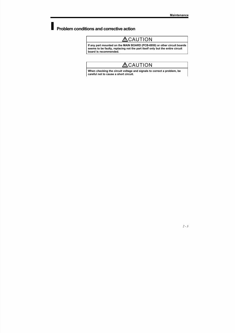
Problem conditions and corrective action
CAUTIONIf any part mounted on the MAIN BOARD (PCB-6950) or other circuit boardsseems to be faulty, replacing not the part itself only but the entire circuitboard is recommended.
CAUTIONWhen checking the circuit voltage and signals to correct a problem, becareful not to cause a short circuit.

8/13/2019 Manual de Service Fcp-7101 - Fx-7102
http://slidepdf.com/reader/full/manual-de-service-fcp-7101-fx-7102 24/170
Chapter 2
2 - 4
Unit doesn't start up when main power is switched ON.
Item to Check Method of Checking and Corrective Action Place to Check
Power cable Check that the power cable is plugged into the power
outlet and the AC adaptor. Check that the DC plug
is connected to the equipment.
Power cable
DC plug
LED on the operation panel
Cable
Connect the DC plug and check that the [MainPower] LED on the operation panel is kept ON. If
not, check the KEY cables connecting the operation panel and the MAIN BOARD for a break, etc.
[Main Power] LED on theoperation panel
KEY cable
Fuse Using a voltmeter, check that F6 fuse is not blown. F6 REFERENCE P5-37
Checking the voltageon MAIN BOARD
Using a voltmeter, check that +18V, +5V, +3.3V,+1.8V, +3.3VSTB, and +5VSTB are present atC100, C311, C312, C317, C314, and C310 terminals
of the MAIN BOARD. When +5V or +3.3V is present, LED4 or LED5 is lit.
C100, C310, C311, C312,C314, C317LED4, LED5REFERENCE P5-37,39
AC adaptor Check that the LED of the AC adaptor is lit.
Using a voltmeter, check that +18V is present at DC plug terminal.
LED of AC adaptor
DC plug
Battery operations are not executed.
Item to Check Method of Checking and Corrective Action Place to Check
Battery connection Open the battery compartment cover, and verify thatthe battery pack is securely connected
Battery compartmentREFERENCE P3-2
Checking the charge After the end of charging the battery, start theoperation using the battery.If the operation is impossible or soon fails, the
battery is deteriorated. Replace the battery with anew one.
Starting after charging.
Fuse Using a voltmeter, check that F3 fuse is not blown. F3 REFERENCE P5-37
Checking the voltage
on MAIN BOARD
Using a voltmeter, check that the battery pack
voltage, +5V, +3.3V, +1.8V, and +3.3VSTB are present at C100, C311, C312, C317, and C314
terminals of the MAIN BOARD. When +5V or+3.3V is present, LED4 or LED5 is lit.
C100, C311, C312, C314,
C317LED4, LED5REFERENCE P5-37,39
8/13/2019 Manual de Service Fcp-7101 - Fx-7102
http://slidepdf.com/reader/full/manual-de-service-fcp-7101-fx-7102 25/170
Maintenance
2 - 5
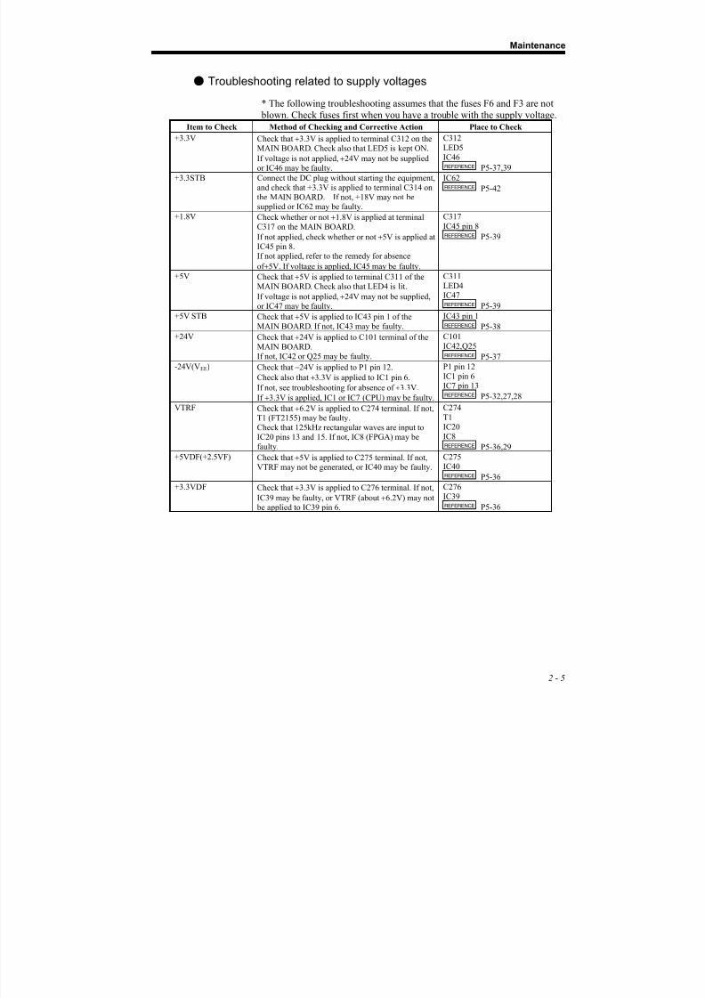
Troubleshooting related to supply voltages
* The following troubleshooting assumes that the fuses F6 and F3 are not
blown. Check fuses first when you have a trouble with the supply voltage.
Item to Check Method of Checking and Corrective Action Place to Check
+3.3V Check that +3.3V is applied to terminal C312 on theMAIN BOARD. Check also that LED5 is kept ON.
If voltage is not applied, +24V may not be suppliedor IC46 may be faulty.
C312
LED5IC46REFERENCE P5-37,39
+3.3STB Connect the DC plug without starting the equipment,and check that +3.3V is applied to terminal C314 onthe MAIN BOARD. If not, +18V may not besupplied or IC62 may be faulty.
IC62REFERENCE P5-42
+1.8V Check whether or not +1.8V is applied at terminalC317 on the MAIN BOARD.
If not applied, check whether or not +5V is applied at
IC45 pin 8.If not applied, refer to the remedy for absence
of +5V. If voltage is applied, IC45 may be faulty.
C317
IC45 pin 8REFERENCE P5-39
+5V Check that +5V is applied to terminal C311 of theMAIN BOARD. Check also that LED4 is lit.
If voltage is not applied, +24V may not be supplied,or IC47 may be faulty.
C311
LED4IC47REFERENCE P5-39
+5V STB Check that +5V is applied to IC43 pin 1 of theMAIN BOARD. If not, IC43 may be faulty.
IC43 pin 1REFERENCE P5-38
+24V Check that +24V is applied to C101 terminal of theMAIN BOARD.If not, IC42 or Q25 may be faulty.
C101IC42,Q25REFERENCE P5-37
-24V(VEE) Check that−
24V is applied to P1 pin 12.Check also that +3.3V is applied to IC1 pin 6.
If not, see troubleshooting for absence of +3.3V.
If +3.3V is applied, IC1 or IC7 (CPU) may be faulty.
P1 pin 12IC1 pin 6IC7 pin 13REFERENCE P5-32,27,28
VTRF Check that +6.2V is applied to C274 terminal. If not,T1 (FT2155) may be faulty.Check that 125kHz rectangular waves are input toIC20 pins 13 and 15. If not, IC8 (FPGA) may be
faulty.
C274
T1IC20IC8REFERENCE P5-36,29
+5VDF(+2.5VF) Check that +5V is applied to C275 terminal. If not,VTRF may not be generated, or IC40 may be faulty.
C275IC40REFERENCE P5-36
+3.3VDF Check that +3.3V is applied to C276 terminal. If not,
IC39 may be faulty, or VTRF (about +6.2V) may not be applied to IC39 pin 6.
C276
IC39REFERENCE P5-36

8/13/2019 Manual de Service Fcp-7101 - Fx-7102
http://slidepdf.com/reader/full/manual-de-service-fcp-7101-fx-7102 26/170
Chapter 2
2 - 6
Failures related to charging operations
Item to Check Method of Checking and Corrective Action Place to Check
Power cable Check that the power cable is plugged into the power
outlet and the AC adaptor. Check that the DC plug isconnected to the equipment.
Power cable
DC plug
Battery Open the battery compartment cover on the botton ofthe unit. Verify that the battery is present and that the
battery and unit are securely connected.Verify also that the connecting cable is notdisconnected/broken.
Connection between the battery and unit
CableREFERENCE P3-2
Battery voltage Check whether or not the battery voltage is +8.0 V orhigher.
Battery voltage
Charge error LED is lit
Item to Check Method of Checking and Corrective Action Place to Check
Battery voltage Check whether or not the battery voltage is +14.4 Vor higher
Battery voltage
Battery temperature Detach the battery from the equipment, and checkwhether the battery is excessively hot or not. The
charge error LED comes on if the batterytemperature exceeds 70°C.
Battery temperatureREFERENCE P3-2
Charging operation ended normally, but the battery is nearly
uncharged.
Item to Check Method of Checking and Corrective Action Place to Check
Battery The number of charge and discharge cycles of battery is about 300 although it depends on the particular operating environment. The duration inhours after charging shortens as the number ofdischarges increases. If the battery cannot hardly be
charged, replace it.
Battery
8/13/2019 Manual de Service Fcp-7101 - Fx-7102
http://slidepdf.com/reader/full/manual-de-service-fcp-7101-fx-7102 27/170
Maintenance
2 - 7
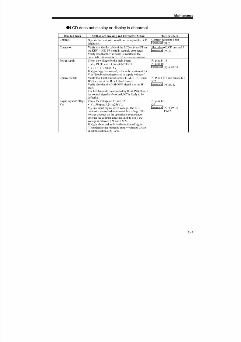
LCD does not display or display is abnormal.
Item to Check Method of Checking and Corrective Action Place to Check
Contrast Operate the contrast control knob to adjust the LCD
brightness.
Contrast adjusting knobREFERENCE P1-2
Connector Verify that the flat cable of the LCD unit and P1 onthe KEY • LCD I/F board is securely connected.
Verify also that the flat cable is inserted in thecorrect direction and is free of cuts and separation.
Flat cable of LCD unit and P1REFERENCE P5-32
Power supply Check the voltage for the main board.
・ VSS: P1 (11 and 14 pins) GND level
・ VDD: P1 (10 pins) +5V
If VSS or VDD is abnormal, refer to the section of +5V in "Troubleshooting related to supply voltages".
P1 pins 11,14P1 pins 10REFERENCE P2-4, P5-32
Control signals Verify that LCD control signals FLM,CL1,CL2 and
D0-3 are not at the H or L fixed levels.
Verify also that the DISPOFF* signal is at the Hlevel.The LCD module is controlled by IC7(CPU); thus, if
the control signal is abnormal, IC7 is likely to bedefective.
P1 Pins 1 to 4 and pins 6, 8, 9
IC7
REFERENCE P5-28, 32
Liquid crystal voltage
VEE
Check the voltage on P1 pins 12.
・ VEE P9 (pins A24, A25) VEE.
VEE is a liquid crystal drive voltage. The LCDcontrast is controlled in terms of this voltage. Thevoltage depends on the operation circumstances.Operate the contrast adjusting knob to see if the
voltage is between +21 and +24 V.If VEE is abnormal, refer to the section of VEE in
"Troubleshooting related to supply voltages". Alsocheck the action of Q1 area.
P1 pins 12
Q1REFERENCE P2-4, P5-32
P5-27
8/13/2019 Manual de Service Fcp-7101 - Fx-7102
http://slidepdf.com/reader/full/manual-de-service-fcp-7101-fx-7102 28/170
Chapter 2
2 - 8
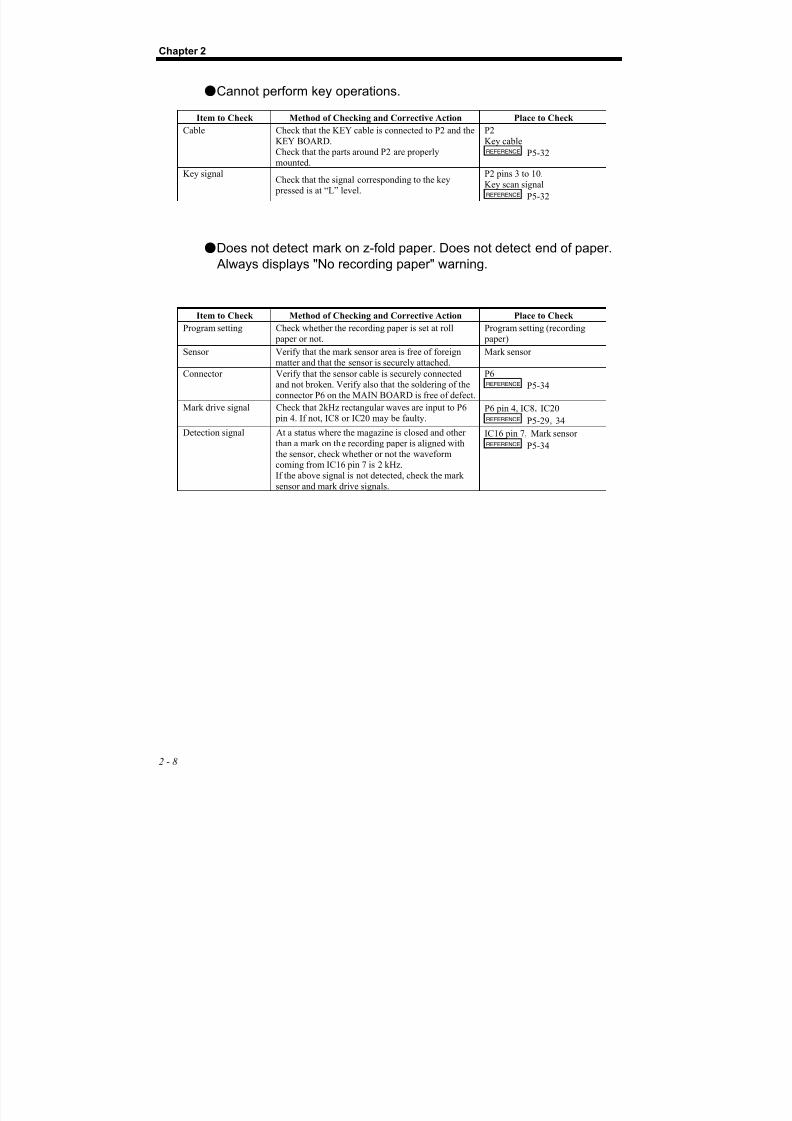
Cannot perform key operations.
Item to Check Method of Checking and Corrective Action Place to Check
Cable Check that the KEY cable is connected to P2 and the
KEY BOARD.Check that the parts around P2 are properlymounted.
P2
Key cableREFERENCE P5-32
Key signalCheck that the signal corresponding to the key pressed is at “L” level.
P2 pins 3 to 10.
Key scan signalREFERENCE P5-32
Does not detect mark on z-fold paper. Does not detect end of paper.
Always displays "No recording paper" warning.
Item to Check Method of Checking and Corrective Action Place to Check
Program setting Check whether the recording paper is set at roll paper or not.
Program setting (recording paper)
Sensor Verify that the mark sensor area is free of foreignmatter and that the sensor is securely attached.
Mark sensor
Connector Verify that the sensor cable is securely connectedand not broken. Verify also that the soldering of theconnector P6 on the MAIN BOARD is free of defect.
P6REFERENCE P5-34
Mark drive signal Check that 2kHz rectangular waves are input to P6
pin 4. If not, IC8 or IC20 may be faulty.
P6 pin 4, IC8,IC20REFERENCE P5-29,34
Detection signal At a status where the magazine is closed and otherthan a mark on the recording paper is aligned withthe sensor, check whether or not the waveformcoming from IC16 pin 7 is 2 kHz.If the above signal is not detected, check the mark
sensor and mark drive signals.
IC16 pin 7,Mark sensorREFERENCE P5-34
8/13/2019 Manual de Service Fcp-7101 - Fx-7102
http://slidepdf.com/reader/full/manual-de-service-fcp-7101-fx-7102 29/170
Maintenance
2 - 9
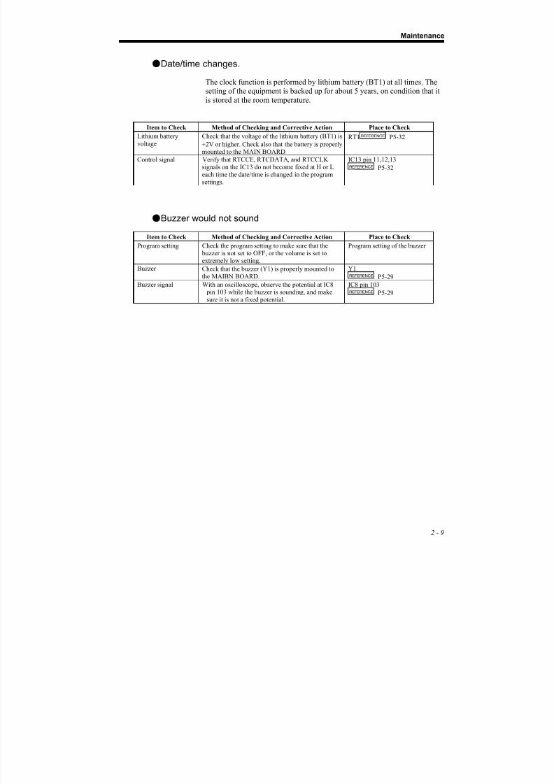
Date/time changes.
The clock function is performed by lithium battery (BT1) at all times. The
setting of the equipment is backed up for about 5 years, on condition that it
is stored at the room temperature.
Item to Check Method of Checking and Corrective Action Place to Check
Lithium battery
voltage
Check that the voltage of the lithium battery (BT1) is
+2V or higher. Check also that the battery is properlymounted to the MAIN BOARD.
RT1REFERENCE P5-32
Control signal Verify that RTCCE, RTCDATA, and RTCCLKsignals on the IC13 do not become fixed at H or Leach time the date/time is changed in the program
settings.
IC13 pin 11,12,13REFERENCE P5-32
Buzzer would not sound
Item to Check Method of Checking and Corrective Action Place to Check
Program setting Check the program setting to make sure that the buzzer is not set to OFF, or the volume is set toextremely low setting.
Program setting of the buzzer
Buzzer Check that the buzzer (Y1) is properly mounted tothe MAIBN BOARD.
Y1REFERENCE P5-29
Buzzer signal With an oscilloscope, observe the potential at IC8
pin 103 while the buzzer is sounding, and makesure it is not a fixed potential.
IC8 pin 103REFERENCE P5-29
8/13/2019 Manual de Service Fcp-7101 - Fx-7102
http://slidepdf.com/reader/full/manual-de-service-fcp-7101-fx-7102 30/170
Chapter 2
2 - 10
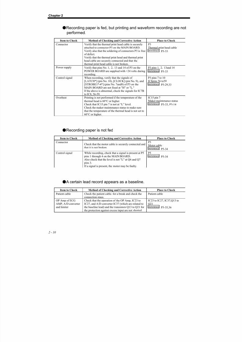
Recording paper is fed, but printing and waveform recording are not
performed.
Item to Check Method of Checking and Corrective Action Place to Check
Connector Verify that the thermal print head cable is securely
attached to connector P3 on the MAIN BOARD.Verify also that the soldering of connectors P3 is freeof defect.Verify that the thermal print head and thermal printhead cable are securely connected and that thethermal print head cable is not broken.
P3
Thermal print head cableREFERENCE P5-33
Power supply Verify that pins No. 1,2,13 and 14 of P3 on the
POWER BOARD are supplied with +24 volts duringrecording.
P3 pins 1,2,13and 14REFERENCE P5-33
Control signal When recording, verify that the signals of
[LATCH*] (pin No. 10), [CLOCK] (pin No. 9), and
[STROBE1*-4*] (pins No. 7and8) of P3 on theMAIN BOARD are not fixed at "H" or "L."If the above is abnormal, check the signals for IC7Bto IC8, 56-59.
P3 pins 7 to 10
IC8pins 56 to59
REFERENCE P5-29,33
Overheat Printing is not performed if the temperature of the
thermal head is 60°C or higher.Check that IC15 pin 7 is not at “L” level.Check the maker maintenance status to make sure
that the temperature of the thermal head is not set to
60°C or higher.
IC15 pin 7Maker maintenance statusREFERENCE P5-33, P3-14
Recording paper is not fed
Item to Check Method of Checking and Corrective Action Place to Check
ConnectorCheck that the motor cable is securely connected andthat it is not broken.
P5Motor cableREFERENCE P5-34
Control signal While recording, check that a signal is present at P5
pins 1 through 4 on the MAIN BOARD.Also check that the level is not "L" at Q6 and Q7 pins 3.If a signal is present, the motor may be faulty.
P5REFERENCE P5-34
A certain lead record appears as a baseline.
Item to Check Method of Checking and Corrective Action Place to Check
Patient cable Check the patient cable. for a break and check theconnection staus.
Patient cable
OP Amp of ECGAMP, A/D converterand limiter
Check that the operation of the OP Amp, IC23 toIC27, and A/D converter IC37 (which are related tothe baseline lead) and the transistors Q13 to Q21 for
the protection against excess input are not shorted.
IC23 to IC27, IC37,Q13 toQ21REFERENCE P5-35,36

8/13/2019 Manual de Service Fcp-7101 - Fx-7102
http://slidepdf.com/reader/full/manual-de-service-fcp-7101-fx-7102 31/170
Maintenance
2 - 11
All 12-lead patient records appear as baselines.
Item to Check Method of Checking and Corrective Action Place to Check
Control signal Check that 125kHz rectangular waves are input to
IC20 pin 13.Check also that reversed rectangular waves are inputto IC20 pin 15.
IC20 pins 13,15REFERENCE P5-36
Supply voltage of
ECG AMP
Power may not be supplied.
See troubleshooting on supply voltage (2-4 and 2-5).
REFERENCE P2-5
ECG AMP clock Check that 8MHz rectangular waves are output from
X2 pin 3. If not, X2 may be faulty.
X2 pins 3REFERENCE P5-36
ECG AMP signal Check that IC38 pins 5 and 7, [RXD] and [TXD], are
not set to “H” or fixed to “L.”
IC38 pins 5 and 7REFERENCE P5-36“CPLD(IC38) peripheralcircuit”
Detection of electrode misposition cannot be led.
Item to Check Method of Checking and Corrective Action Place to Check
Patient signal of ECGAMP
Check the signal line (around IC23 and IC24) whereelectrode misposition occurred.
Signal lines of ECG AMP(around IC23 and IC24)REFERENCE P5-35
Some leads do not detect electrode misposition.
Because of the high impedance circuit structure, the portion of ECG inputthat precedes the buffer IC is difficult to measure with an instrument. Thus,
from a time standpoint, it is effective to determine faulty locations by
replacing devices.
Item to Check Method of Checking and Corrective Action Place to Check
OP Amp Under the condition where the electrode mispositionoccurs (patient cable disconnected, etc.), check that
the output voltage of buffer OP Amp related to thelead not detecting the electrode misposition (IC23and IC24) is approximately –2.5V.
IC23, IC24REFERENCE P5-35
Multiplexer Check if the electrode misposition signal is properlyinput to IC29. IC29.REFERENCE P5-35
ECG AMP limiter Under the condition where the electrode mispositionoccurs (patient cable disconnected, etc.), remove thetransistors Q13 to Q21 for the protection againstexcess input related to the lead not detecting theelectrode misposition, and check the operation.
Q13 to Q21REFERENCE P5-35

8/13/2019 Manual de Service Fcp-7101 - Fx-7102
http://slidepdf.com/reader/full/manual-de-service-fcp-7101-fx-7102 32/170
Chapter 2
2 - 12
8/13/2019 Manual de Service Fcp-7101 - Fx-7102
http://slidepdf.com/reader/full/manual-de-service-fcp-7101-fx-7102 33/170
Chapter 3
MaintenanceCleaning...............................................................................................3-1
Cleaning the unit ..................................................................... 3-1 Replacing the battery..........................................................................3-2Update of the software........................................................................3-4Self-diagnostics test...........................................................................3-5
User self-diagnostics test........................................................3-6ECG Test Pattern................................................................ 3-7Recording Test.................................................................... 3-8
Key Test ..............................................................................3-9LCD Test ...........................................................................3-10Buzzer Test ....................................................................... 3-11
Manufacturer self-diagnostics test......................................... 3-12Status Test ........................................................................3-14ECG A/D DATA .................................................................3-15LAN Test ...........................................................................3-16Memory Test ..................................................................... 3-17ROM WRITE Test .............................................................3-18Recorder Test ...................................................................3-19Memory initialize ...............................................................3-21
Update...............................................................................3-22Periodical inspections ......................................................................3-23
Periodical inspection intervals and precautions ....................3-23List of periodical inspection items .........................................3-23Safety inspections (4 items)..................................................3-24
Before checking the leakage current ................................ 3-24
Checking the enclosure leakage current
(current that flows from the enclosure to
the earth terminal of the power outlet)............................. 3-25
Checking the patient leakage current I..............................3-25Checking the patient leakage current III............................3-25
Checking the patient measurement current ...................... 3-25

8/13/2019 Manual de Service Fcp-7101 - Fx-7102
http://slidepdf.com/reader/full/manual-de-service-fcp-7101-fx-7102 34/170
Inspection of electrical performance/characteristics..............3-26
Hardware inspections (10 items)...........................................3-28
Periodical inspection(2) record........................................................3-30
8/13/2019 Manual de Service Fcp-7101 - Fx-7102
http://slidepdf.com/reader/full/manual-de-service-fcp-7101-fx-7102 35/170
Chapter 3 Maintenance
3 - 1
Cleaning
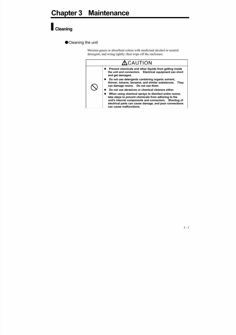
Cleaning the unit
Moisten gauze or absorbent cotton with medicinal alcohol or neutral
detergent, and wring tightly; then wipe off the enclosure.
CAUTION Prevent chemicals and other liquids from getting inside
the unit and connectors. Electrical equipment can shortand get damaged.
Do not use detergents containing organic solvent,
thinner, toluene, benzene, and similar substances. Theycan damage resins. Do not use them.
Do not use abrasives or chemical cleaners either.
When using chemical sprays to disinfect entire rooms,take steps to prevent chemicals from adhering to theunit's internal components and connectors. Shorting ofelectrical parts can cause damage, and poor connectionscan cause malfunctions.
8/13/2019 Manual de Service Fcp-7101 - Fx-7102
http://slidepdf.com/reader/full/manual-de-service-fcp-7101-fx-7102 36/170
Chapter 3
3 - 2
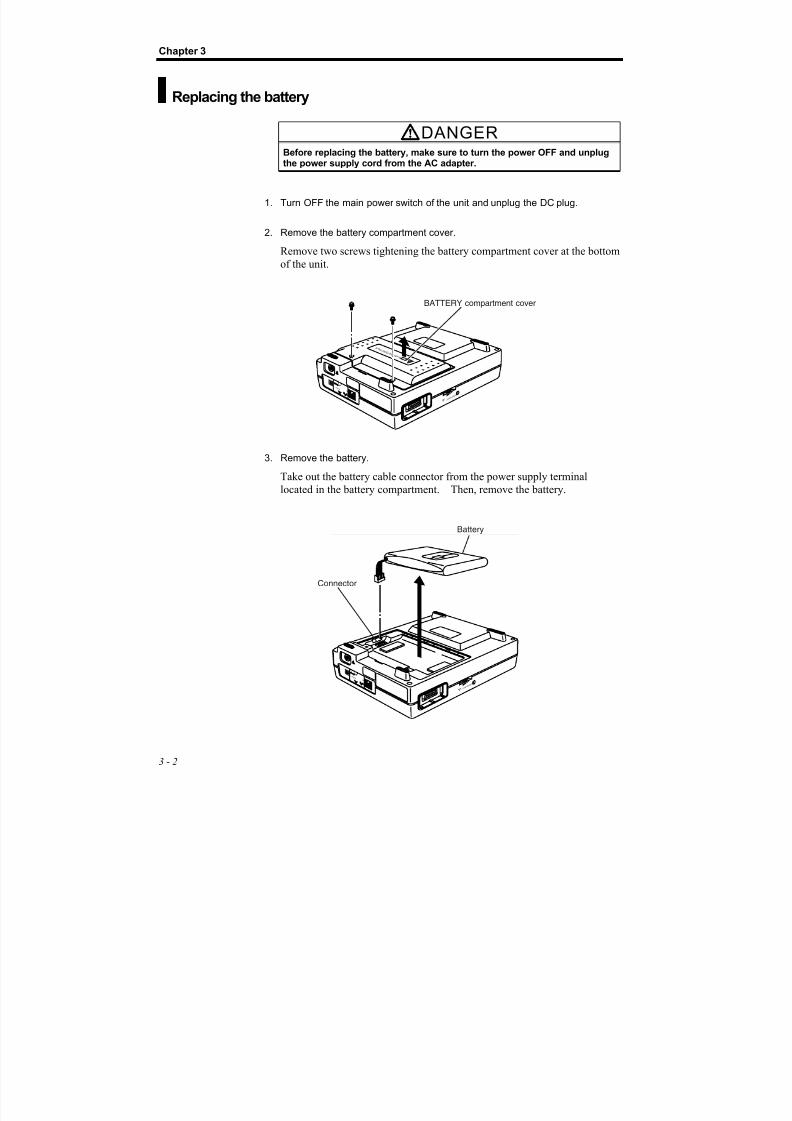
Replacing the battery
DANGERBefore replacing the battery, make sure to turn the power OFF and unplugthe power supply cord from the AC adapter.
1. Turn OFF the main power switch of the unit and unplug the DC plug.
2. Remove the battery compartment cover.
Remove two screws tightening the battery compartment cover at the bottom
of the unit.
C O N T R A S T
BATTERY compartment cover
L A M D C I N 1 8 V
N i - M H B A T T E R Y P A C K
3. Remove the battery.
Take out the battery cable connector from the power supply terminal
located in the battery compartment. Then, remove the battery.
Connector
Battery
C O N T R A S T
L A M D C I N 1
8 V
8/13/2019 Manual de Service Fcp-7101 - Fx-7102
http://slidepdf.com/reader/full/manual-de-service-fcp-7101-fx-7102 37/170
Maintenance
3 - 3
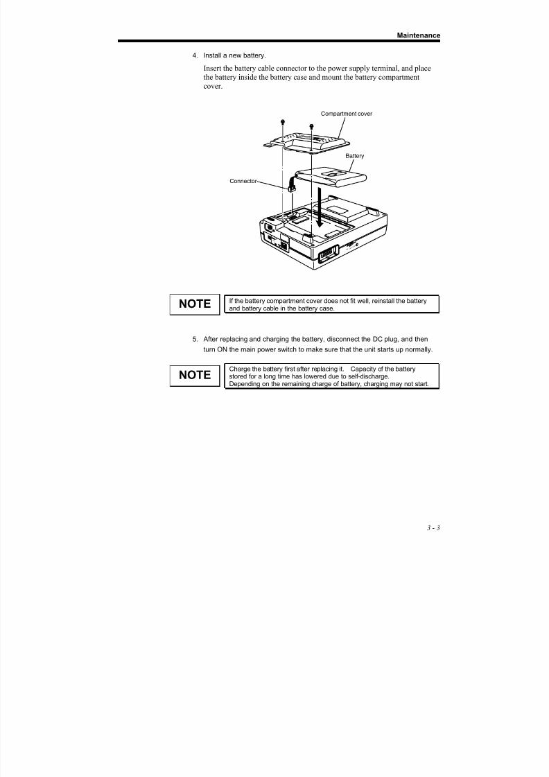
4. Install a new battery.
Insert the battery cable connector to the power supply terminal, and place
the battery inside the battery case and mount the battery compartment
cover.
C O N T R A S T
Connector
Battery
Compartment cover
L A M D C I N 1
8 V
N i - M H B A T T E R Y P A C K
If the battery compartment cover does not fit well, reinstall the batteryand battery cable in the battery case.
5. After replacing and charging the battery, disconnect the DC plug, and then
turn ON the main power switch to make sure that the unit starts up normally.
Charge the battery first after replacing it. Capacity of the batterystored for a long time has lowered due to self-discharge.
Depending on the remaining charge of battery, charging may not start.
NOTE
NOTE
8/13/2019 Manual de Service Fcp-7101 - Fx-7102
http://slidepdf.com/reader/full/manual-de-service-fcp-7101-fx-7102 38/170
Chapter 3
3 - 4
Update of the software
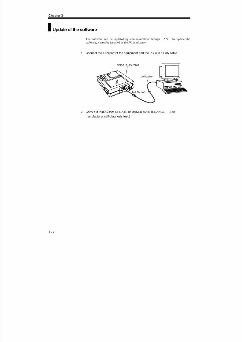
The software can be updated by communication through LAN. To update the
software, it must be installed in the PC in advance.
1. Connect the LAN port of the equipment and the PC with a LAN cable.
M O D E
F C P - 7 1 0 1
M a i n P o w e r
O N / O F F
( s t b y )
C h a n g e
P O W E R
O F F : H O L D 2 S e c .
L E A D 1 m V
R E S E T
S E N S E
S T A R T / S T O P I D
E N T E R
C A N S E L
To LAN port
LAN cable
FCP-7101/FX-7102
LAM
DCIN18V
2. Carry out PROGRAM UPDATE of MAKER MAINTENANCE. (See
manufacturer self-diagnosis test.)
8/13/2019 Manual de Service Fcp-7101 - Fx-7102
http://slidepdf.com/reader/full/manual-de-service-fcp-7101-fx-7102 39/170
Maintenance
3 - 5
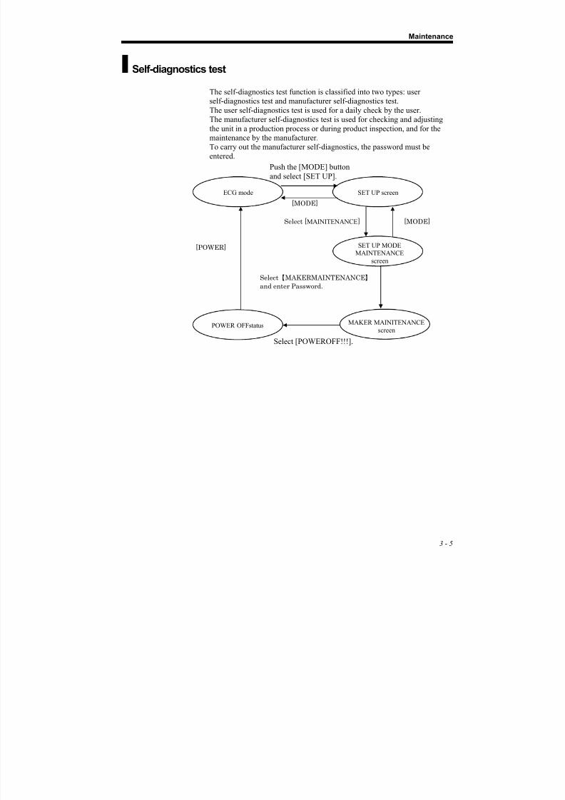
Self-diagnostics test
The self-diagnostics test function is classified into two types: user
self-diagnostics test and manufacturer self-diagnostics test.The user self-diagnostics test is used for a daily check by the user.
The manufacturer self-diagnostics test is used for checking and adjusting
the unit in a production process or during product inspection, and for the
maintenance by the manufacturer.
To carry out the manufacturer self-diagnostics, the password must be
entered.
ECG mode SET UP screen
SET UP MODEMAINTENANCE
screen
MAKER MAINITENANCE
screen
Select [POWEROFF!!!].
Select [MAINITENANCE] [MODE]
Push the [MODE] button
and select [SET UP].
[MODE]
Select 【MAKERMAINTENANCE】 and enter Password.
[POWER]
POWER OFFstatus

8/13/2019 Manual de Service Fcp-7101 - Fx-7102
http://slidepdf.com/reader/full/manual-de-service-fcp-7101-fx-7102 40/170
Chapter 3
3 - 6
User self-diagnostics test
Push the [MODE] key and select [SET UP] using the [→] key. Push the
[↓] key to display the pull-down menu. Select [MAINTENANCE] from
the menu using the [ ↑ ] [ ↓ ] key. Then push the [ENTER] key, and the[SETUP MODE (MAINTENANCE)] screen is displayed. Select a
desired user self-diagnostic menu using the [ ↑ ] [ ↓ ] key, and a
corresponding diagnosis screen is displayed.
The following user self-diagnostic test menus are available.
• ECG TEST PATTERN• RECORDING TEST
• KEY TEST
• LCD TEST
• BUZZER TEST
Push the [MODE] key to return to the SETUP pull-down menu selection
screen.
8/13/2019 Manual de Service Fcp-7101 - Fx-7102
http://slidepdf.com/reader/full/manual-de-service-fcp-7101-fx-7102 41/170
Maintenance
3 - 7
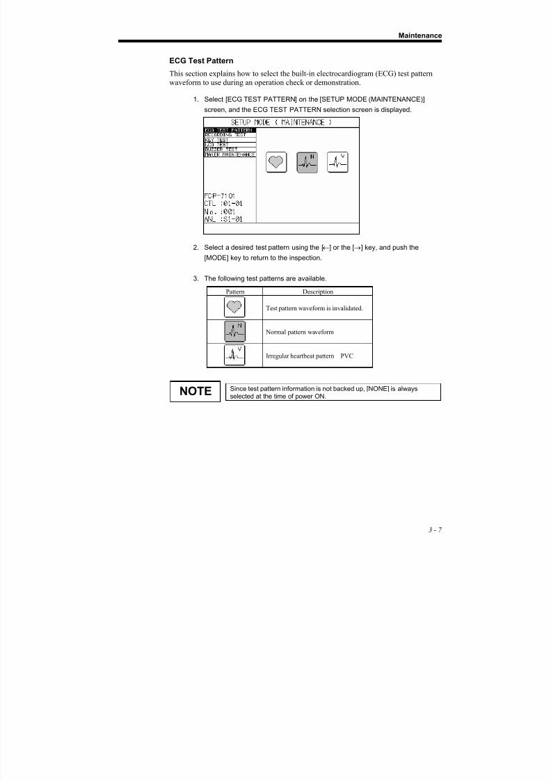
ECG Test Pattern
This section explains how to select the built-in electrocardiogram (ECG) test pattern
waveform to use during an operation check or demonstration.
1. Select [ECG TEST PATTERN] on the [SETUP MODE (MAINTENANCE)]
screen, and the ECG TEST PATTERN selection screen is displayed.
2. Select a desired test pattern using the [←] or the [→] key, and push the
[MODE] key to return to the inspection.
3. The following test patterns are available.
Pattern Description
Test pattern waveform is invalidated.
Normal pattern waveform
Irregular heartbeat pattern PVC
Since test pattern information is not backed up, [NONE] is alwaysselected at the time of power ON.
NOTE
8/13/2019 Manual de Service Fcp-7101 - Fx-7102
http://slidepdf.com/reader/full/manual-de-service-fcp-7101-fx-7102 42/170
Chapter 3
3 - 8
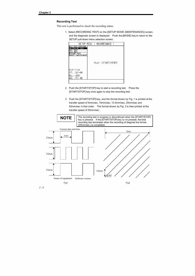
Recording Test
This test is performed to check the recording status.
1. Select [RECORDING TEST] on the [SETUP MODE (MAINTENANCE)] screen,
and the diagnosis screen is displayed. Push the [MODE] key to return to the
SETUP pull-down menu selection screen.
2. Push the [START/STOP] key to start a recording test. Press the
[START/STOP] key once again to stop the recording test.
3. Push the [START/STOP] key, and the format shown by Fig. 1 is printed at the
transfer speed of 5mm/sec, 10mm/sec, 12.5mm/sec, 25mm/sec and
50mm/sec in that order. The format shown by Fig. 2 is then printed at the
transfer speed of 50mm/sec.
The recording test in progress is discontinued when the [START/STOP]key is pressed. If the [START/STOP] key is not pressed, the totalrecording test terminates when the recording of diagonal line format(25mm/sec.) is completed.
15mm 1sec
5sec
15mm
15mm
Current date and time
Name of equipment Software version
60°
10mm
Fig1 Fig2
NOTE
8/13/2019 Manual de Service Fcp-7101 - Fx-7102
http://slidepdf.com/reader/full/manual-de-service-fcp-7101-fx-7102 43/170
Maintenance
3 - 9
Key Test
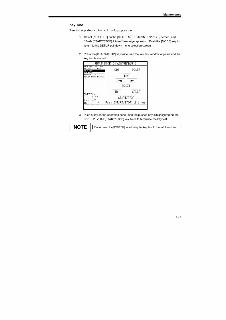
This test is performed to check the key operation.
1. Select [KEY TEST] on the [SETUP MODE (MAINTENANCE)] screen, and
“Push [START/STOP] 2 times” message appears. Push the [MODE] key to
return to the SETUP pull-down menu selection screen.
2. Press the [START/STOP] key twice, and the key test window appears and the
key test is started.
3. Push a key on the operation panel, and the pushed key is highlighted on the
LCD. Push the [START/STOP] key twice to terminate the key test.
Press down the [POWER] key during the key test to turn off the power.NOTE

8/13/2019 Manual de Service Fcp-7101 - Fx-7102
http://slidepdf.com/reader/full/manual-de-service-fcp-7101-fx-7102 44/170
8/13/2019 Manual de Service Fcp-7101 - Fx-7102
http://slidepdf.com/reader/full/manual-de-service-fcp-7101-fx-7102 45/170
Maintenance
3 - 11
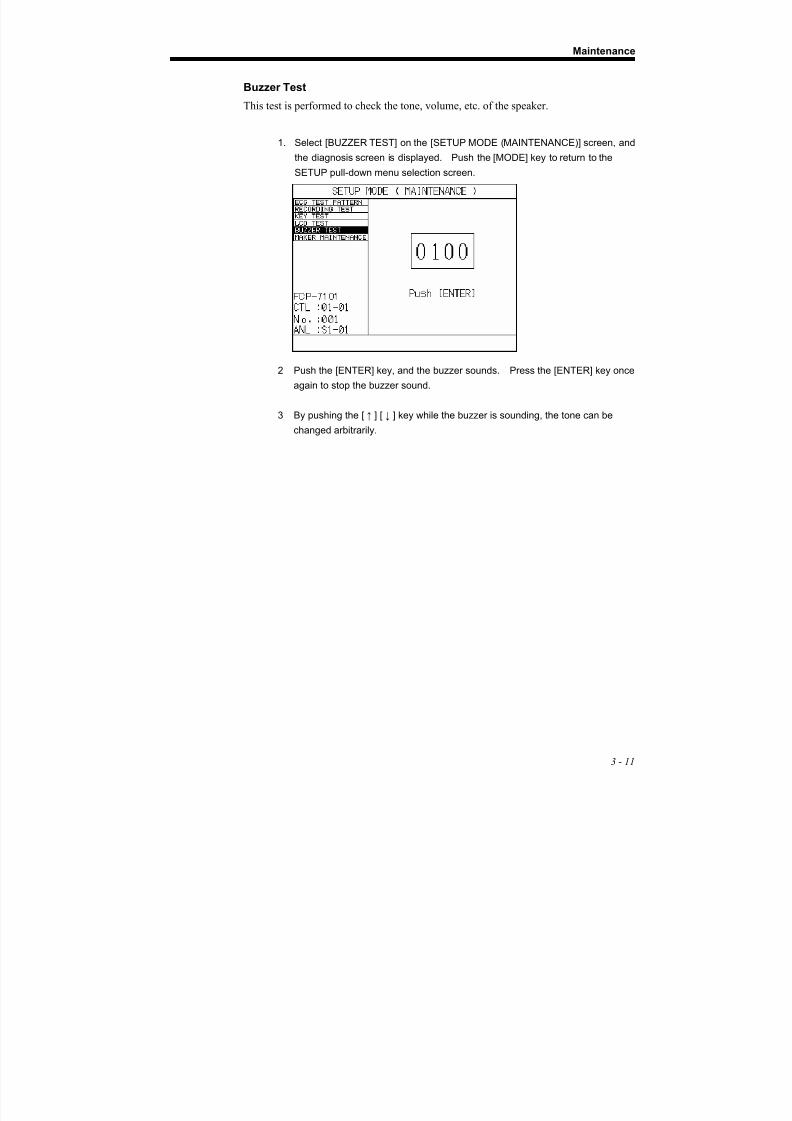
Buzzer Test
This test is performed to check the tone, volume, etc. of the speaker.
1. Select [BUZZER TEST] on the [SETUP MODE (MAINTENANCE)] screen, and
the diagnosis screen is displayed. Push the [MODE] key to return to the
SETUP pull-down menu selection screen.
2 Push the [ENTER] key, and the buzzer sounds. Press the [ENTER] key once
again to stop the buzzer sound.
3 By pushing the [ ↑ ] [ ↓ ] key while the buzzer is sounding, the tone can bechanged arbitrarily.
8/13/2019 Manual de Service Fcp-7101 - Fx-7102
http://slidepdf.com/reader/full/manual-de-service-fcp-7101-fx-7102 46/170
Chapter 3
3 - 12
Manufacturer self-diagnostics test
Select [MAKER MAINTENANCE] on the [SETUP MODE
(MAINTENANCE)] screen and enter the password, and the [MAKER
MAINTENANCE] screen is displayed. Manufacturer self-diagnostic test
can be performed on this screen. Manufacturer self-diagnostic test is
usually performed by the personnel of the manufacturer in charge of
maintenance. The following tests can be performed as manufacturer
self-diagnostic tests.
• STATUS TEST
• ECG A/D DATA
• LAN TEST
• MEMORY TEST
• ROM WRITE TEST
• RECORDER TEST• ROM INITIALIZE
• PROGRAM UPDATE
Enter the password as follows.
1. Select [MAKER MAINTENANCE] on the [SETUP MODE (MAINTENANCE)]
screen, and the following screen is displayed. Push the [MODE] key to return
to the SETUP pull-down menu selection screen.

8/13/2019 Manual de Service Fcp-7101 - Fx-7102
http://slidepdf.com/reader/full/manual-de-service-fcp-7101-fx-7102 47/170
Maintenance
3 - 13
2. Enter the password (9001) using the up/down/right/left key and push the
[ENTER] key, and the [MAKER MAINTENANCE] screen appears, allowing
you to perform manufacturer self-diagnostic test. Select a desired diagnostic
item to go to the corresponding diagnosis screen.
3. Push [POWER OFF!!!], and the ECG is turned off and the manufacturer
self-diagnostic test is terminated.
You cannot return to the ECG mode screen in MAKER MAINTENANCEmode. To go to the ECG mode screen, turn off the power by selecting[POWER OFF!!!] and start the equipment once again..
NOTE

8/13/2019 Manual de Service Fcp-7101 - Fx-7102
http://slidepdf.com/reader/full/manual-de-service-fcp-7101-fx-7102 48/170
Chapter 3
3 - 14
Status Test
This test is performed to check the function of displaying each status of the hardware.
1. Select [STATUS TEST] on the [MAKER MAINTENANCE] screen, and the
following screen is displayed.
2. The following status information is displayed in [STATUS TEST].
• Thermal head temperature
• Lithium battery voltage
• Battery voltage
• Battery temperature
• Mark sensor voltage• Sensor voltage for detection of paper out
• Recorder status (magazine up)
8/13/2019 Manual de Service Fcp-7101 - Fx-7102
http://slidepdf.com/reader/full/manual-de-service-fcp-7101-fx-7102 49/170
Maintenance
3 - 15
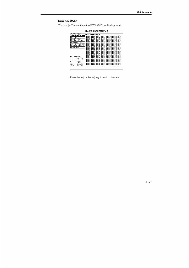
ECG A/D DATA
The data (A/D value) input to ECG AMP can be displayed.
1. Press the [←] or the [→] key to switch channels.
8/13/2019 Manual de Service Fcp-7101 - Fx-7102
http://slidepdf.com/reader/full/manual-de-service-fcp-7101-fx-7102 50/170
Chapter 3
3 - 16
LAN Test
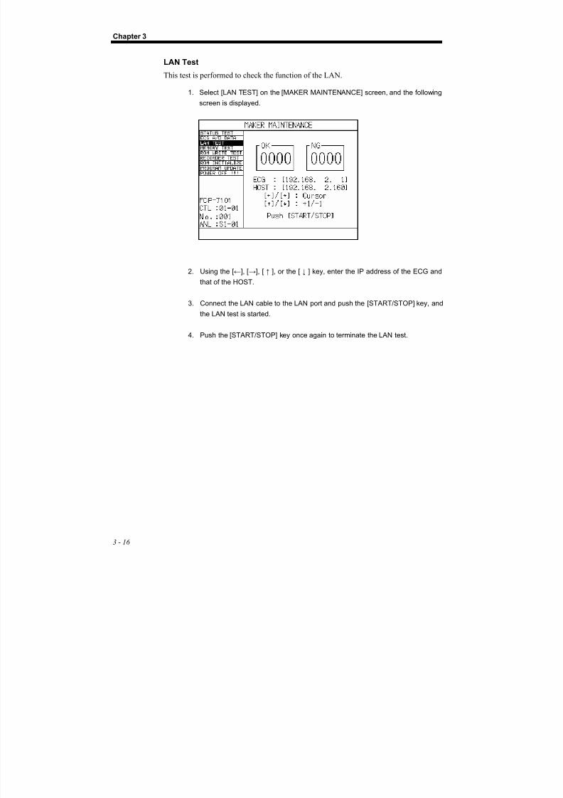
This test is performed to check the function of the LAN.
1. Select [LAN TEST] on the [MAKER MAINTENANCE] screen, and the following
screen is displayed.
2. Using the [←], [→], [ ↑ ], or the [ ↓ ] key, enter the IP address of the ECG and
that of the HOST.
3. Connect the LAN cable to the LAN port and push the [START/STOP] key, and
the LAN test is started.
4. Push the [START/STOP] key once again to terminate the LAN test.

8/13/2019 Manual de Service Fcp-7101 - Fx-7102
http://slidepdf.com/reader/full/manual-de-service-fcp-7101-fx-7102 51/170
Maintenance
3 - 17
Memory Test
This test is performed to check the read/write status of the SDRAM.
1. Select [MEMORY TEST] on the [MAKER MAINTENANCE] screen, and the
following screen is displayed.
2. Push the [START/STOP] key to start the memory test.
3. Push the [START/STOP] key once again to terminate the memory test.
8/13/2019 Manual de Service Fcp-7101 - Fx-7102
http://slidepdf.com/reader/full/manual-de-service-fcp-7101-fx-7102 52/170
Chapter 3
3 - 18
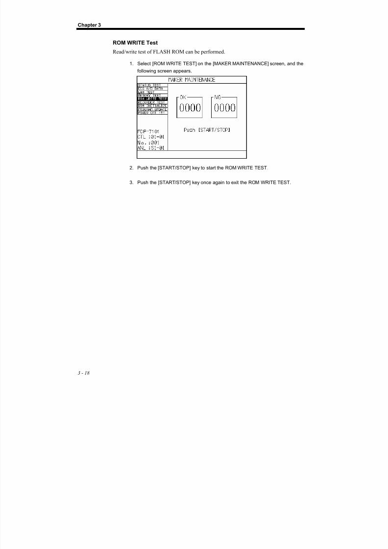
ROM WRITE Test
Read/write test of FLASH ROM can be performed.
1. Select [ROM WRITE TEST] on the [MAKER MAINTENANCE] screen, and the
following screen appears.
2. Push the [START/STOP] key to start the ROM WRITE TEST.
3. Push the [START/STOP] key once again to exit the ROM WRITE TEST.

8/13/2019 Manual de Service Fcp-7101 - Fx-7102
http://slidepdf.com/reader/full/manual-de-service-fcp-7101-fx-7102 53/170
Maintenance
3 - 19
Recorder Test
The recorder test is a function of checking the thermal head for missing dots and
verifying the printing condition.
1. Select [RECORDER TEST] on the [MAKER MAINTENANCE] screen, and the
following screen is displayed.
2. Select the pattern to be printed using the right/left key.
Pattern Process
Prints dot pattern.
Prints rectangular waveforms in the format shown by Fig.3.
Prints diagonal lines in the format shown by Fig. 4.
Fig. 3 Fig. 4
1ch 15mm
3ch 15mm
60°10mm

8/13/2019 Manual de Service Fcp-7101 - Fx-7102
http://slidepdf.com/reader/full/manual-de-service-fcp-7101-fx-7102 54/170
Chapter 3
3 - 20
3. Push the [START/STOP] key to start a recorder test. Select transfer speed
using the right/left key while printing is underway.
4. Push the [START/STOP] key once again to terminate the recorder test.
50mm/S5mm/S 10mm/S 12.5mm/S 25mm/S
8/13/2019 Manual de Service Fcp-7101 - Fx-7102
http://slidepdf.com/reader/full/manual-de-service-fcp-7101-fx-7102 55/170
Maintenance
3 - 21
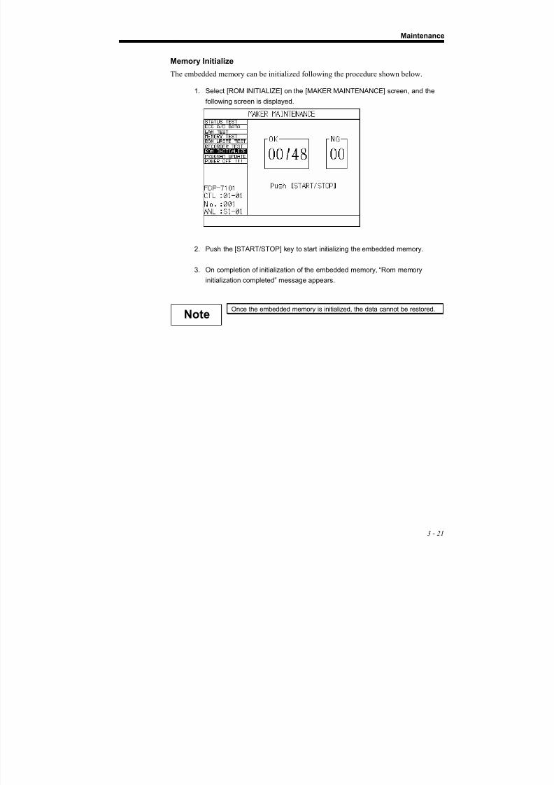
Memory Initialize
The embedded memory can be initialized following the procedure shown below.
1. Select [ROM INITIALIZE] on the [MAKER MAINTENANCE] screen, and the
following screen is displayed.
2. Push the [START/STOP] key to start initializing the embedded memory.
3. On completion of initialization of the embedded memory, “Rom memory
initialization completed” message appears.
Once the embedded memory is initialized, the data cannot be restored.Note
8/13/2019 Manual de Service Fcp-7101 - Fx-7102
http://slidepdf.com/reader/full/manual-de-service-fcp-7101-fx-7102 56/170
Chapter 3
3 - 22
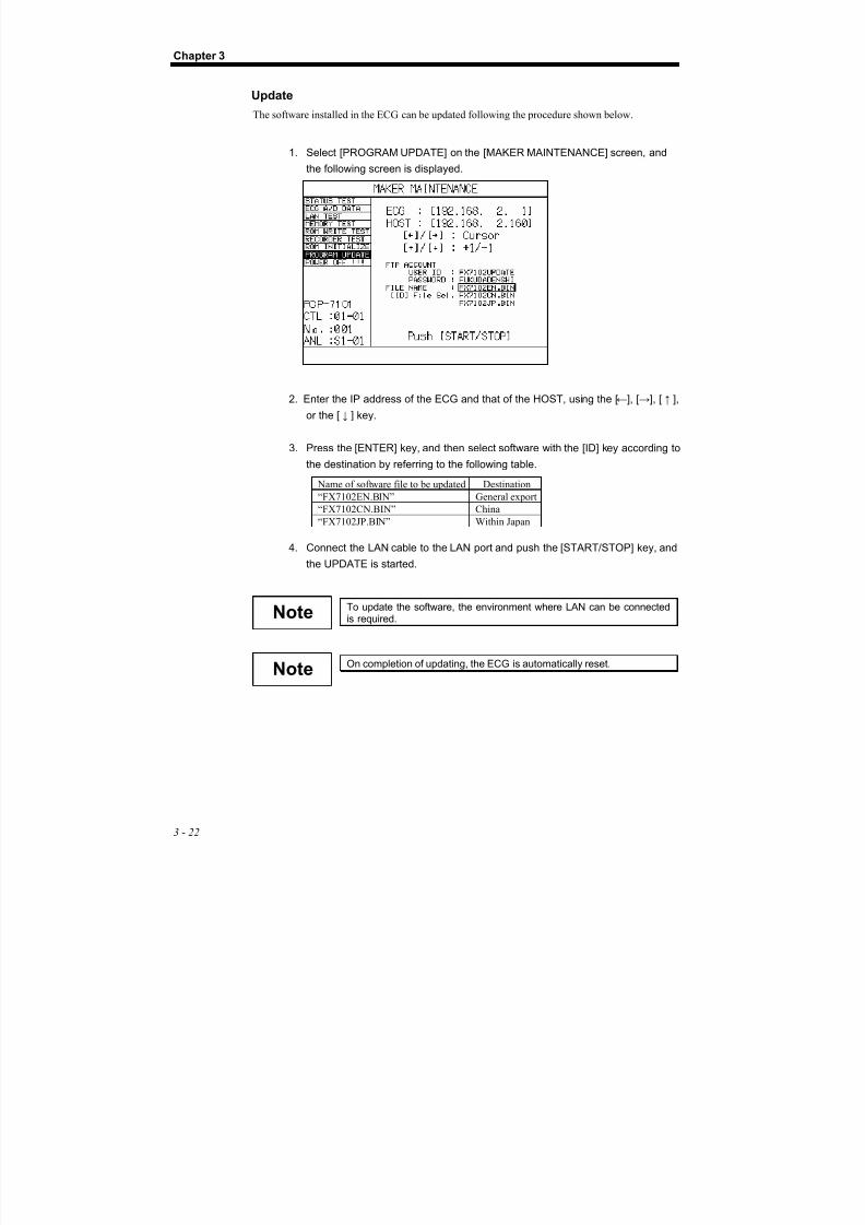
Update
The software installed in the ECG can be updated following the procedure shown below.
1. Select [PROGRAM UPDATE] on the [MAKER MAINTENANCE] screen, and
the following screen is displayed.
2. Enter the IP address of the ECG and that of the HOST, using the [←], [→], [ ↑ ],
or the [ ↓ ] key.
3. Press the [ENTER] key, and then select software with the [ID] key according to
the destination by referring to the following table.
Name of software file to be updated Destination
“FX7102EN.BIN” General export
“FX7102CN.BIN” China
“FX7102JP.BIN” Within Japan
4. Connect the LAN cable to the LAN port and push the [START/STOP] key, and
the UPDATE is started.
To update the software, the environment where LAN can be connectedis required.
On completion of updating, the ECG is automatically reset.
Note
Note
8/13/2019 Manual de Service Fcp-7101 - Fx-7102
http://slidepdf.com/reader/full/manual-de-service-fcp-7101-fx-7102 57/170
Maintenance
3 - 23
Periodical inspections
To maintain the unit's functions and performance, periodical inspections are
required.The inspections explained in this section should be performed by service
representatives who have sufficient technical knowledge.
Periodical inspection intervals and precautions
Inspection item Description
Periodical inspection interval Periodical inspection should be performed at least
once a year.
Precautions before inspection Simplified circuits that are used to measure protectiveearth resistance are illustrated; however, fire, electric
shock, and other hazards accompany the manufactureand use of such circuits. Handle with care.
Precautions after inspection After the inspection is completed, clean each part.
Measuring device used forinspection
Electronic voltmeter or digital voltmeter
List of periodical inspection items
Inspection item Description
Safety inspection Enclosure leakage current inspectionPatient leakage current I inspection
Patient leakage current III inspectionPatient measurement current inspection
Inspection ofelectrical performance/characteristics
SensitivityTime constant (AMP)Frequency characteristicControl of in-phase signalCounter electrode voltageInternal noise
Recording sensitivity
Hardware inspection Patient cable/connecting cable inspectionLimb electrode/chest electrode inspection
Recording paper/Keratin cream inspectionOperation Manual inspection
Trolley/cord hanger inspection (if any)Enclosure inspectionRating label inspectionSwitch inspectionPower supply fuse inspectionRecorder inspectionElectrode inspection

8/13/2019 Manual de Service Fcp-7101 - Fx-7102
http://slidepdf.com/reader/full/manual-de-service-fcp-7101-fx-7102 58/170
Chapter 3
3 - 24
Safety inspections (4 items)
To assure safety of medical equipment, testing methods and measurement
equipment are prescribed in the safety test standards with respect to leakage
current that affects human body. To perform inspections, make the settingand pass/fail evaluation using a leakage current gauge that meets the
requirements for measurement of medical equipment.
WARNINGIf, during a safety inspection, a value that exceeds the allowable limit isdetected, immediately stop using the unit and replace the defective part ormake proper repairs. Otherwise a serious accident may result.
Before checking the leakage current
There are a number of conditions for measuring leakage current. Adopt
the maximum value obtained as measurement value.
It is also very important to compare the obtained value with past
measurement values to confirm that no significant difference is observed.
To measure the leakage current, use a leakage current gauge provided with
human body simulation impedance (network) as shown below.
Measure the voltage at both ends of the human body simulation impedance,
and substitute the obtained value into the following formula to obtain
current value.
Measured voltage (V)
1000= Measured current (mA)
About leakage current gaugeSince leakage current has significant effect on human body, testing methods,
performance of measuring instrument, value limit of leakage current, etc.
are specified by various laws and standards. Use a measuring instrument
conforming to “IEC 60601-1,” which is standard specification of electrical
appliances for medical application, to measure the leakage current of this
instrument.
8/13/2019 Manual de Service Fcp-7101 - Fx-7102
http://slidepdf.com/reader/full/manual-de-service-fcp-7101-fx-7102 59/170
Maintenance
3 - 25
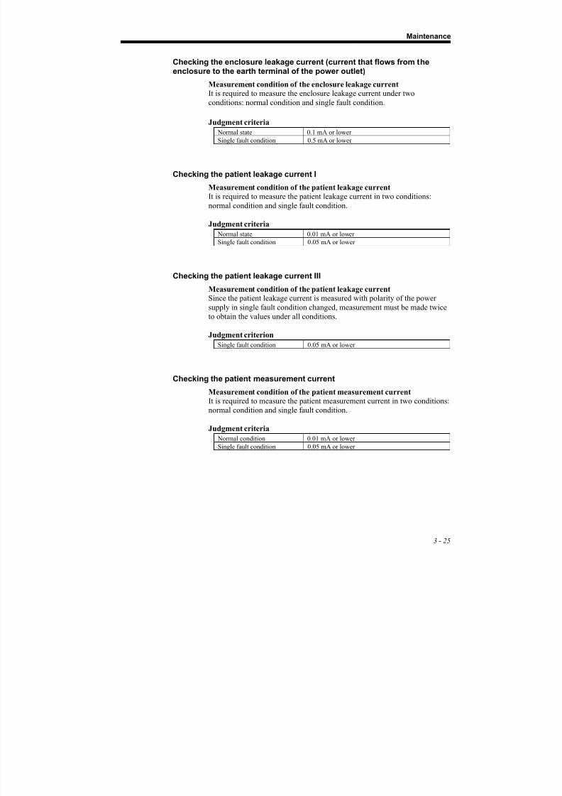
Checking the enclosure leakage current (current that flows from theenclosure to the earth terminal of the power outlet)
Measurement condition of the enclosure leakage current
It is required to measure the enclosure leakage current under two
conditions: normal condition and single fault condition.
Judgment criteria
Normal state 0.1 mA or lower
Single fault condition 0.5 mA or lower
Checking the patient leakage current I
Measurement condition of the patient leakage current
It is required to measure the patient leakage current in two conditions:normal condition and single fault condition.
Judgment criteria
Normal state 0.01 mA or lower
Single fault condition 0.05 mA or lower
Checking the patient leakage current III
Measurement condition of the patient leakage current
Since the patient leakage current is measured with polarity of the power
supply in single fault condition changed, measurement must be made twice
to obtain the values under all conditions.
Judgment criterion
Single fault condition 0.05 mA or lower
Checking the patient measurement current
Measurement condition of the patient measurement currentIt is required to measure the patient measurement current in two conditions:
normal condition and single fault condition.
Judgment criteria
Normal condition 0.01 mA or lower
Single fault condition 0.05 mA or lower
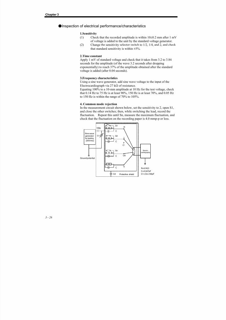
8/13/2019 Manual de Service Fcp-7101 - Fx-7102
http://slidepdf.com/reader/full/manual-de-service-fcp-7101-fx-7102 60/170
Chapter 3
3 - 26
Inspection of electrical performance/characteristics
1.Sensitivity
(1) Check that the recorded amplitude is within 10±0.2 mm after 1 mV
of voltage is added to the unit by the standard voltage generator.
(2) Change the sensitivity selector switch to 1/2, 1/4, and 2, and check
that standard sensitivity is within ±5%.
2.Time constant
Apply 1 mV of standard voltage and check that it takes from 3.2 to 3.84
seconds for the amplitude (of the wave 3.2 seconds after dropping
exponentially) to reach 37% of the amplitude obtained after the standard
voltage is added (after 0.04 seconds).
3.Frequency characteristicsUsing a sine wave generator, add sine wave voltage to the input of the
Electrocardiograph via 27 k Ω of resistance.
Equating 100% to a 10-mm amplitude at 10 Hz for the test voltage, check
that 0.14 Hz to 75 Hz is at least 90%, 150 Hz is at least 70%, and 0.05 Hz
to 150 Hz is within the range of 70% to 105%.
4. Common mode rejection
In the measurement circuit shown below, set the sensitivity to 2, open S1,
and close the other switches; then, while switching the lead, record the
fluctuation. Repeat this until Sn, measure the maximum fluctuation, and
check that the fluctuation on the recording paper is 4.0 mmp-p or less.
R
R
R
R
Sine wavegeneratorfor testing(20Vrms)
100p
Ground potential
C1
C2
Electro-cardiography
C
C
C
C
S1
S2
Sn
R
L
N
C6
FC1
Protective shield
R=51KΩ
C=0.047pF
C1+C2=100pF
8/13/2019 Manual de Service Fcp-7101 - Fx-7102
http://slidepdf.com/reader/full/manual-de-service-fcp-7101-fx-7102 61/170
Maintenance
3 - 27
5.Counter electrode voltage
(1) Check that the change in the recorded sensitivity is within ±5%
when ±550 mV of DC voltage is imposed to the input of the
Electrocardiograph.
(2) Check that the change in the recorded sensitivity is within ±5%
when ±550 mV of DC voltage is imposed between the two input
terminals of the Electrocardiograph and the RF(N) electrode fitting.
6.Internal noise
Make shortcircuited the each terminal of all input terminals with the
parallel impedance with 51k Ω and 47nF. Place the baseline at the center
at each lead selection position, set the sensitivity to 2, and record the noise.
Check that the size of the noise on the recorded line is 0.4 mmp-p or
smaller at random 0.2-second intervals.
7.Recording speedConnect a clock that provides the unit with signal voltage at 1-second
intervals, and record the pulse waveform. Check that the error in transfer
speed at speeds of 5mm/sec, 10 mm/sec, 12.5mm/sec, 25 mm/sec, and 50
mm/sec is within ±3%.
8/13/2019 Manual de Service Fcp-7101 - Fx-7102
http://slidepdf.com/reader/full/manual-de-service-fcp-7101-fx-7102 62/170
Chapter 3
3 - 28
Hardware inspections (10 items)
WARNINGIf, during a hardware inspection, you notice damage or other abnormality,immediately stop using the given unit; then replace the defective part,replenish, or make proper repairs.Failure to repair the unit can lead to a serious accident.Do not replace the part nor carry out refilling or the like but change thehardware (MAIN BOARD, for ex.) found faulty. If the trouble cannot beremedied by replacing any part, for example, the guarantee clause of thesupplier will nopushply to the relevant hardware.
Checking the patient cable/connecting cable
DescriptionCheck the patient cable/connecting cable for open circuit, the covered area
for damage, and the connector pins for interference/rust/contamination.
Checking the limb electrode/chest electrode
Description
Check for adherence of dust and rust.
Checking the recording paper/Keratin cream
Description
Check that they are set correctly.Checking the operation manual
Description
Check that it is stored in the correct place without any damage.
Checking the trolley/cord hanger (if any)
Description
Check that trolley body's installation status, trolley's exterior, casters' status,
and cord hanger's exterior, and also check the mounting screws for
looseness.
Checking the enclosure
Description
Check the enclosure of the unit for flaws, cracks, deformation, rust, and
other exterior defects.
Checking the rating label
Description
Check the rating label for separation, cleanliness, legibility, and other
exterior defects.

8/13/2019 Manual de Service Fcp-7101 - Fx-7102
http://slidepdf.com/reader/full/manual-de-service-fcp-7101-fx-7102 63/170
Maintenance
3 - 29
Checking the switches
Description
Check for unsmooth operation, damage, and rattling.
Checking the recorder
Description
Check that recording operation is smoothly performed and no abnormal
noise exists.
Checking the electrodes
Description
Check the electrodes for corrosion, and their chip-mounting area for wear,
safety defects, malfunctional operation, and damage.

8/13/2019 Manual de Service Fcp-7101 - Fx-7102
http://slidepdf.com/reader/full/manual-de-service-fcp-7101-fx-7102 64/170
Chapter 3
3 - 30
Periodical inspection(2) record
Item Description
Procedure/measurement value
Acceptance standard
Judge-
ment
Remarks
(Repairrequired
1. Power supply cord, patient cable, etc. Any flaws or damages? OK ・ NG
2. Limb electrode, chest electrode, etc. Any contamination or rust adhered? OK ・ NG
3. Recording paper/Keratin cream Correctly set? OK ・ NG
4. Operation Manual Stored in a correct place? OK ・ NG
Cables
Electrodes
Consumables
Accessories5. Trolley/cord hanger, etc. Any damages? OK ・ NG
1. Flaws/cracks/deformation/rust onenclosure
Any damages? OK ・ NG
2. Peel-off or dirt on rating label or panel Display visible? OK ・ NG V i s u a l i n s p e c t i o n
Appearance
3. Key Any damages? OK ・ NG
1. Key Smoothly move? OK ・ NGMain unit
2. Recorder Smoothly move? Any abnormal noise? OK ・ NG
1. Power supply cord, patient cable Any rattling? OK ・ NG M e c h a n i c a l
Accessories2. Electrodes Any problem in connection? OK ・ NG
1. Status Are thermal head temperature, lithium battery voltage, mark sensor status, andrecording paper detection operation
normal in the status test?
OK ・ NG
2. LAN Is LAN communication normal? OK ・ NG
3. Memory Any abnormality on pass and errorcounts?
OK ・ NG
4. ROM Is write to ROM normal? OK ・ NG
5. Recorder adjustmentIs the location of thermal print head
correct when recorder is moved?
OK ・ NG
M a n u
f a c t u r e r s e l f - d i a g n o s t i c s
Performance
6. Power OFF Does pressing of the ENTER keynormally turn off the power?
OK ・ NG
Cleaning and
disinfection
1. Cleaning, disinfection, pasteurization,
and sterilizationOK ・ NG
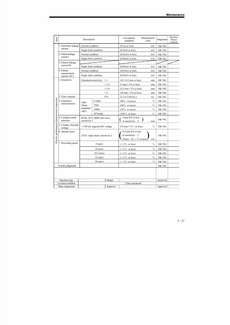
8/13/2019 Manual de Service Fcp-7101 - Fx-7102
http://slidepdf.com/reader/full/manual-de-service-fcp-7101-fx-7102 65/170
Maintenance
3 - 31
I t e m
Description
(Acceptance
standard)
Measurement
value Judgement
Remarks
(Repairrequired
Normal condition (0.1m or less) mA OK ・ NG1. Enclosure leakagecurrent
Single fault condition (0.5mA or less) mA OK ・ NG
Normal condition (0.01mA or less) mA OK ・ NG2. Patient leakage
current ISingle fault condition (0.05mA or less) mA OK ・ NG
3. Patient leakagecurrent III
Single fault condition (0.05mA or less) mA OK ・ NG
Normal condition (0.01mA or less) mA OK ・ NG4. Patient
measurementcurrent (AC) Single fault condition (0.05mA or less) mA OK ・ NG
(Standard sensitivity) ×1 (10±0.2 mm or less) mm OK ・ NG
×1/2 (5 mm±5% or less) mm OK ・ NG
×1/4 (2.5 mm±5% or less) mm OK ・ NG
1. Sensitivity
×2 (20 mm±5% or less) mm OK ・ NG
2. Time constant 37% (3.2 to 3.84 sec.) sec OK ・ NG
0.14Hz (90% or more) % OK ・ NG
75Hz (90% or more) % OK ・ NG
150Hz (70% or more) % OK ・ NG
3. Frequencycharacteristics 10Hz・
10mm
amplitude
100% All bonds (105% or less) % OK ・ NG
4. Common mode
rejection
60 Hz, 20 V, RMS sine wave,
sensitivity 2
4 mm P-P or less
at sensitivity 2 mm OK ・ NG
5. Counter electrodevoltage
±550 mV imposed DC voltage (10 mm±5% or less) % OK ・ NG
6. Internal noise
27k Ω input short, sensitivity 2
0.4 mm P-P or less
at sensitivity 2
(Noise : 20 μV or less) mm
OK ・ NG
5 mm/s (±3% or less) % OK ・ NG
10 mm/s (±3% or less) % OK ・ NG
12.5 mm/s (±3% or less) % OK ・ NG
25 mm/s (±3% or less) % OK ・ NG
E l e c t r i c p e r f o r m a n c e / c h a r a c t e r i s t i c s i n s p e c t i o n
7. Recording speed
50 mm/s (±3% or less) % OK ・ NG
Overall judgement OK ・ NG
Machine type Model Serial No.
Location installed Date purchased
Date inspected Inspector Approval
( )
( )

8/13/2019 Manual de Service Fcp-7101 - Fx-7102
http://slidepdf.com/reader/full/manual-de-service-fcp-7101-fx-7102 66/170
Chapter 3
3 - 32
8/13/2019 Manual de Service Fcp-7101 - Fx-7102
http://slidepdf.com/reader/full/manual-de-service-fcp-7101-fx-7102 67/170
Chapter 4
DisassemblyRemoving the LCD .....................................................................4-1Removing the enclosure cover.................................................4-2Removing the recorder unit ......................................................4-3Removing the main board ......................................................... 4-4

8/13/2019 Manual de Service Fcp-7101 - Fx-7102
http://slidepdf.com/reader/full/manual-de-service-fcp-7101-fx-7102 68/170

8/13/2019 Manual de Service Fcp-7101 - Fx-7102
http://slidepdf.com/reader/full/manual-de-service-fcp-7101-fx-7102 69/170
Disassembly
4 -1
Removing the LCD
1. Press the magazine open button and remove the paper magazine.
F C P - 7 1
0 1 M a
i n
P o w e
r C h a
r g e
M O D E
P O W E R
O F F : H
O L D 2 s
e c .
L E A D
1 m V
R E S E T
S E N S E
S T A
R T / S T O
P
I D
E N T E R
C A N C E L
O N / O F F
( s t b y )
Paper magazine
Magazine open button 2. Remove the mounting screws (four).
C O N T R A S T
L A M D C I N 1 8 V
N i - M H B A T T E R Y
P A C K
Mounting screw
3. Open the top cover.
4. Remove the nuts (three) fastening the LCD.
5. Lift the LCD and remove the shield plate placed under the LCD.

8/13/2019 Manual de Service Fcp-7101 - Fx-7102
http://slidepdf.com/reader/full/manual-de-service-fcp-7101-fx-7102 70/170
Chapter 4
4 -2
6. Remove the LCD cable connected to connector P1.
LA M D CI N1 8 V
Nut
LCD module
LCD cable
Shield plate
P1 Removing the enclosure cover
1. Remove the LCD
For details on removing procedures, see page4-1, “Removing the LCD”.
2. Remove the KEY cable connected to connector P2.
LA M D CI N1 8 V
P2
Key cable
Enclosure cover
REFERENCE
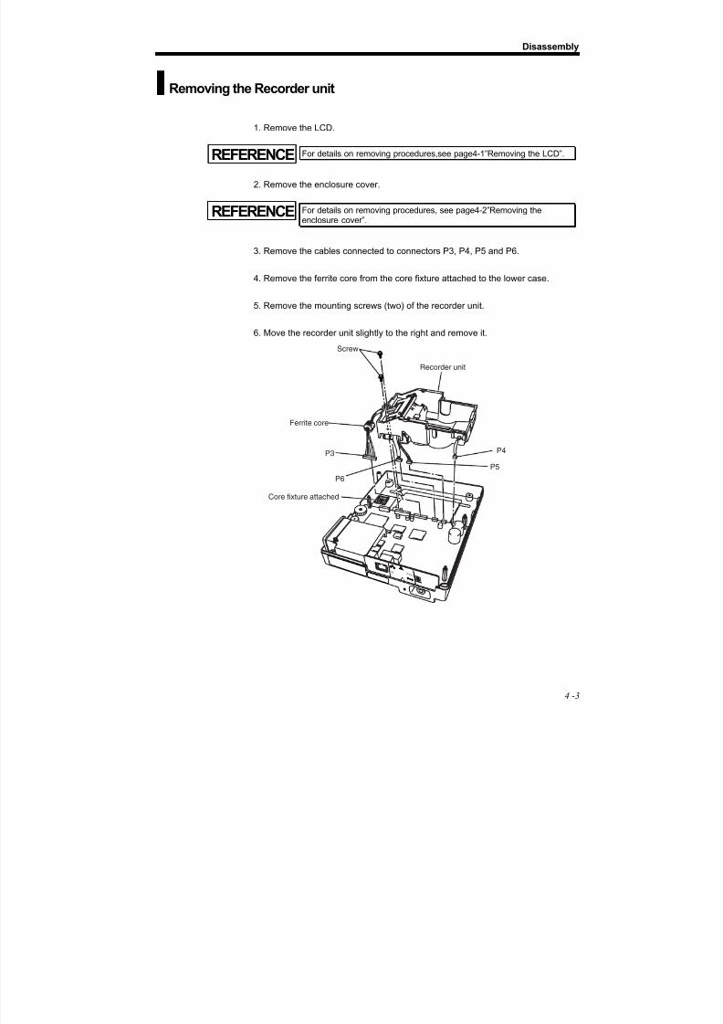
8/13/2019 Manual de Service Fcp-7101 - Fx-7102
http://slidepdf.com/reader/full/manual-de-service-fcp-7101-fx-7102 71/170
Disassembly
4 -3
Removing the Recorder unit
1. Remove the LCD.
For details on removing procedures,see page4-1”Removing the LCD”.
2. Remove the enclosure cover.
For details on removing procedures, see page4-2”Removing theenclosure cover”.
3. Remove the cables connected to connectors P3, P4, P5 and P6.
4. Remove the ferrite core from the core fixture attached to the lower case.
5. Remove the mounting screws (two) of the recorder unit.
6. Move the recorder unit slightly to the right and remove it.
P5
P6
P3
Screw
P4
Recorder unit
LA M D CI N1 8 V
Ferrite core
Core fixture attached
REFERENCE
REFERENCE
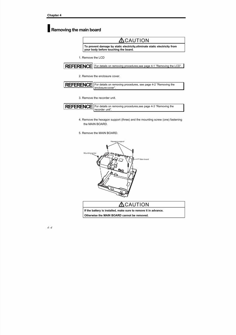
8/13/2019 Manual de Service Fcp-7101 - Fx-7102
http://slidepdf.com/reader/full/manual-de-service-fcp-7101-fx-7102 72/170
Chapter 4
4 -4
Removing the main board
CAUTIONTo prevent damage by static electricity,eliminate static electricity fromyour body before touching the board.
1. Remove the LCD
For details on removing procedures,see page 4-1 ”Removing the LCD”.
2. Remove the enclosure cover.
For details on removing procedures, see page 4-2 ”Removing theenclosure cover”.
3. Remove the recorder unit.
For details on removing procedures,see page 4-3 “Removing therecorder unit”.
4. Remove the hexagon support (three) and the mounting screw (one) fastening
the MAIN BOARD.
5. Remove the MAIN BOARD.
Main board
Mounting screw
Hexagon support
CAUTIONIf the battery is installed, make sure to remove it in advance.
Otherwise the MAIN BOARD cannot be removed.
REFERENCE
REFERENCE
REFERENCE

8/13/2019 Manual de Service Fcp-7101 - Fx-7102
http://slidepdf.com/reader/full/manual-de-service-fcp-7101-fx-7102 73/170
Chapter 5
Electric Circuit DiagramsOverall block diagram of unit (AC adaptor not included)................5-1
MAIN BOARD block diagram .....................................................5-3
MAIN BOARD (PCB-6950) circuit ..............................................5-51.Digital logic block .................................................................5-5
CPU section........................................................................5-5FPGA section......................................................................5-5Memory section ..................................................................5-6KEY I/F section ...................................................................5-8Thermal head control section..............................................5-9Real time clock .................................................................5-10Reset circuit section.......................................................... 5-11Sensor control section ......................................................5-12Motor control section.........................................................5-13LCD voltage generating section........................................5-14
2.ECG AMP block .................................................................5-153.Power supply block ............................................................5-16
Power voltage generating section.....................................5-17Battery charging section ...................................................5-20
Power control section........................................................5-21KEY BOARD (PCB-6949) circuit ..............................................5-22SENSOR BOARD (PCB-6948) circuit ......................................5-23MAG UP BOARD (PCB-6951) circuit .......................................5-23
AC adaptor block diagram................................................................5-24MAIN BOARD Circuit Diagrams (PCB-6950) ................................... 5-25
Power connection table No.1....................................................5-25Power connection table No.2....................................................5-26POWER /CAPACITOR/REST IC/CLOCKLCD POWER block ..................................................................5-27CPU block ................................................................................5-28
FPGA block ..............................................................................5-29MEMORY block........................................................................5-30LAN CONTROL block...............................................................5-31LCD I/F / RTC / LED block .......................................................5-32THERMAL I/F block..................................................................5-33

8/13/2019 Manual de Service Fcp-7101 - Fx-7102
http://slidepdf.com/reader/full/manual-de-service-fcp-7101-fx-7102 74/170
SENSOR I/F /MAGAZIN UP SENSOR I/FMOTOR I/F /JTAG I/F block ..................................................5-34ECG AMP block(Differential amplification, multiplexer section) ......................5-35ECG AMP block (ADC,CPLD and POWER section) .............5-36
MAIN POWER SUPPLY +24V block .....................................5-37CHARGE block .....................................................................5-38+5V /+3.3V /+1.8V Power generation block ..........................5-39POWER STATUS block.........................................................5-40POWER / CHARGE ERROR block.......................................5-41+3.3VSTB / +1.8V POWER ON RESET block ......................5-42BATTERY ON CONTROL / THERMAL POWERGENERATION BLOCK .........................................................5-43POWER-MAIN I / F block......................................................5-44POWER ON / OFF CONTROL block ....................................5-45
KEY BOARD (PCB-6949)...................................................................5-46SENSOR BOARD (PCB-6948)...........................................................5-47MAG UP BOARD (PCB-6951)............................................................5-48
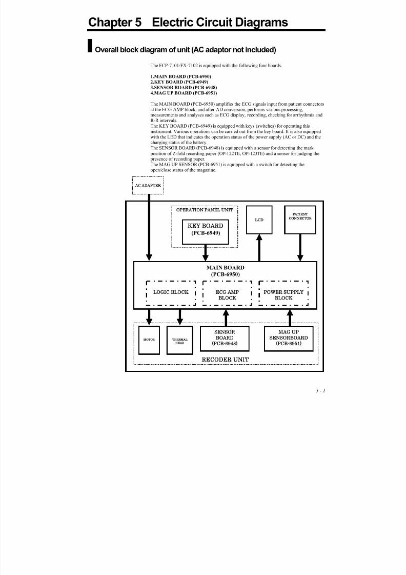
8/13/2019 Manual de Service Fcp-7101 - Fx-7102
http://slidepdf.com/reader/full/manual-de-service-fcp-7101-fx-7102 75/170
Chapter 5 Electric Circuit Diagrams
5 - 1
Overall block diagram of unit (AC adaptor not included)
The FCP-7101/FX-7102 is equipped with the following four boards.
1.MAIN BOARD (PCB-6950)
2.KEY BOARD (PCB-6949)
3.SENSOR BOARD (PCB-6948)
4.MAG UP BOARD (PCB-6951)
The MAIN BOARD (PCB-6950) amplifies the ECG signals input from patient connectorsat the ECG AMP block, and after AD conversion, performs various processing,measurements and analyses such as ECG display, recording, checking for arrhythmia andR-R intervals.The KEY BOARD (PCB-6949) is equipped with keys (switches) for operating thisinstrument. Various operations can be carried out from the key board. It is also equippedwith the LED that indicates the operation status of the power supply (AC or DC) and the
charging status of the battery.The SENSOR BOARD (PCB-6948) is equipped with a sensor for detecting the mark
position of Z-fold recording paper (OP-122TE, OP-123TE) and a sensor for judging the presence of recording paper.
The MAG UP SENSOR (PCB-6951) is equipped with a switch for detecting theopen/close status of the magazine.
MAIN BOARD
(PCB-6950)
SENSOR
BOARD
PCB-6948)
MAG UP
SENSORBOARD
PCB-6951)MOTOR THERMAL
HEAD
LCD
PATIENTCONNECTOR
KEY BOARD
(PCB-6949)
OPERATION PANEL UNIT
RECODER UNIT
LOGIC BLOCK ECG AMP
BLOCK
POWER SUPPLY
BLOCK
AC ADAPTER

8/13/2019 Manual de Service Fcp-7101 - Fx-7102
http://slidepdf.com/reader/full/manual-de-service-fcp-7101-fx-7102 76/170
5 - 2

8/13/2019 Manual de Service Fcp-7101 - Fx-7102
http://slidepdf.com/reader/full/manual-de-service-fcp-7101-fx-7102 77/170

8/13/2019 Manual de Service Fcp-7101 - Fx-7102
http://slidepdf.com/reader/full/manual-de-service-fcp-7101-fx-7102 78/170
5 - 4

8/13/2019 Manual de Service Fcp-7101 - Fx-7102
http://slidepdf.com/reader/full/manual-de-service-fcp-7101-fx-7102 79/170
Electric Circuit Diagrams
5 - 5
MAIN BOARD (PCB-6950) circuit
The main board consists of the following major circuit blocks.
1. Digital logic block2. ECG AMP block
3. Power supply block
1. Digital logic block
CPU section
The CPU adopting SH7727 carries out processing for basic operations of
ECG such as display of ECG waveforms and recording. It also monitors
the voltage of the backup battery and the temperature of the thermal head,
and performs processing related to the mark sensor. The CPU carries out
various other operations such as address bus control, data bus control, and peripheral device control in accordance with the settings of the software.
FPGA section
The FPGA performs the following control operations.
・ ECG control
・ Various types of timing control
・ Thermal control
・ Motor control
・ Buzzer control
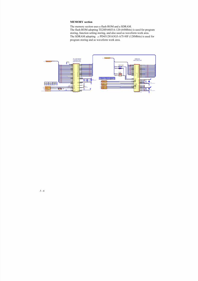
8/13/2019 Manual de Service Fcp-7101 - Fx-7102
http://slidepdf.com/reader/full/manual-de-service-fcp-7101-fx-7102 80/170
5 - 6
MEMORY section
The memory section uses a flash ROM and a SDRAM.
The flash ROM adopting TE28F640J3A-120 (64Mbits) is used for program
storing, function setting storing, and also used as waveform work area.
The SDRAM adopting μPD45128163G5-A75-9JF (128Mbits) is used for
program storing and as waveform work area.
FLASH ROM
RD_LFROMCS_L
WR0_L
RESET_L
+3.3VDG
DG+3.3V
32M/64M/128MIntel Strate Frash
FROMWR_L
JP25
SHORT NORMAL
JP28
OPEN
FROM WR
SHORTOPEN
JTAG
MODE
DG
2
1
+ C1941.0UF/16V(T)3C143
0.01UFFZC144
0.01UFFZ
C1450.01UFFZ
JP28
JP25 0F
CE014
A1213
A1312
A1411
A1510
A221
CE12
CE229
A032
A128
A227
A326
A425
A524
A623
A722
A820
A919
A1018
A1117
A168
A177
A186
A195
A204
A213
DQ033
DQ135
DQ238
DQ340
DQ444
DQ546
DQ649
DQ751
DQ834
DQ936
DQ1039
DQ1141
DQ1245
DQ1347
DQ1450
DQ1552
Vcc9
Vcc37
Vpen15
Vccq43
GND21
GND48
GND42
STS53
OE#54
WE#55
RP#16
BYTE#31
NC56
NC30
IC11
E28F640J3A-120
AB13AB14AB15
AB17
WR1_L
RDWR_LSDRAMCS_L
CKIOCKE
AB15
AB14
AB14
64M/128M
256M
WR0_L
JP26OPENSHORT
JP29 SDRAM TYPE
OPEN 256M64M/128M
JP27 JP30
SHORT+3.3V
DG
DG
+3.3V
SDRAM
2
1
+
C1724.7UF/6.3V(T)3
2
1
+
C1734.7UF/6.3V(T)3
C1460.01UFFZ
C1470.01UFFZ
JP26
0F
JP27 0FAB13
RAS3_LCAS_L
64M/128M/256M
WE16
Vss54
Vssq52
Vccq49
Vssq46
RAS18
CAS17
A023
A124
A225
A326
A429
A530
A631
A732
A833
A934
A10/AP22
A1135
Vccq43
Vss41
NC40
UDQM39
CKE37
DQ02
DQ14
DQ25
DQ37
DQ48
DQ510
DQ611
DQ713
DQ842
DQ944
DQ1045
DQ1147
DQ1248
DQ1350
DQ1451
DQ1553
Vcc1
Vccq9
Vcc14
Vccq3
Vssq6
Vss28
Vssq12
NC36
CS19
BS121
CLK 38
LDQM15
Vcc27
BS020
IC12
UPD45128163G5-A75-9JF
AB16
+3.3V
(4)(4)(4,5)
(4)
(10)
(4)
(4,5)
(4,5)
(3,4,5,8,21)
(4)
(4)
(4)(4,7)
JP29
JP30AB13
AB2AB3AB4AB5AB6AB7AB8
AB1AB2AB3AB4AB5AB6AB7AB8
AB1
AB[1..23]AB[1..23]
AB[1..23]AB[1..15]
AB9AB10AB11AB12
AB9AB10AB11AB12
AB18AB19AB20AB21AB22AB23
(5,7)
(5,7)
DA0DA1DA2DA3DA4DA5DA6DA7DA8DA9DA10DA11DA12DA13DA14DA15
DA0DA1DA2DA3DA4DA5DA6DA7DA8DA9DA10DA11DA12DA13DA14DA15
+3.3V
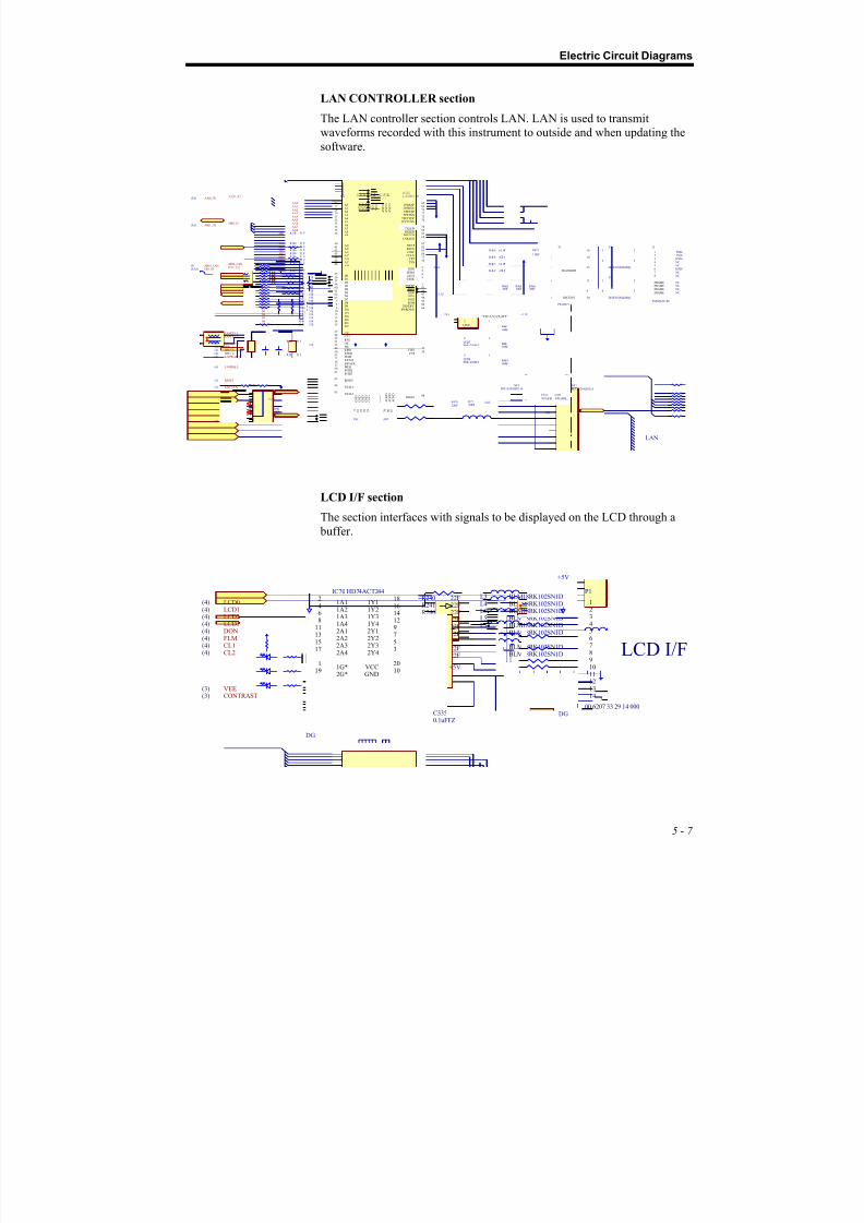
8/13/2019 Manual de Service Fcp-7101 - Fx-7102
http://slidepdf.com/reader/full/manual-de-service-fcp-7101-fx-7102 81/170
Electric Circuit Diagrams
5 - 7
LAN CONTROLLER section
The LAN controller section controls LAN. LAN is used to transmit
waveforms recorded with this instrument to outside and when updating the
software.
LAN
D[0..15]
LANWAIT_LWR3_LWR2_LWR1_L
LANCE1_LLANCE2_L
AA[0..8]
D[0..15]
DG AGL
AGL
DG
LANPWDOWN_L
+3.3V
LANIRQ_L
DG
+3.3V
TRANSMIT
RECEIVE
LINK
A026
A127
A1543
A228
A330
A431
A532
A633
A734
A835
A936
FWE37
FCS39
A1240
A1341
A1442
A1644
A1745
A1846
CE147
D055
D156
D257
D358
D460
D561
D662
D763
D87D9
8
D109
D1110
D1212
D1313
D1414
D1515
XTAL194
XTAL295
V D D
1 9
V D D
3 8
V D D
4 8
V D D
5 9
V D D
9 8
V D D
1 1
A V D D
7 1
A V D D
7 9
A V D D
8 9
G N D
1 0 0
G N D
6
G N D
1 6
G N D
2 2
G N D
2 9
G N D
5 4
G N D
6 4
G N D
9 2
A G N D
7 8
A G N D
8 6
A G N D
8 7
RBIAS88
TPERXP85
TPERXN84
TPETXP75
TPETXN73
TPETXDP72
TPETXDN74
EEDI3
EEDO2
EECS4
EESK 5
PWRDWN66
XENDEC90
EN1691
ROM 93
ENEEP1
IOS096
IOS197
IOS299
REG52
RESET65
WE25
CE224
OE51
IORD49
IOWR 50
WAIT53
IOCS1623
IREQ17
INPACK 18
INTR220
INTR321
TXLED70
RXLED69
BSELED67
LNKLED68
RECP83
COLP81
COLN80
TXP77
TXN76
RECN82
IC55LAN91C96
RESET
R443680F
R444680F
R445680F
R463300F
R464300F
R465300F
R46 6 6 1. 9F
R46 7 6 1. 9F
R46 8 4 22 F
R46 9 4 22 F
C3310.01uFBJ
C3320.01uFBJ
R2210KF
R47012KF
AGL
R471
1.2KF
R47 2 5 1F
R 44 7 5 1FR 44 8 5 1FR 44 9 5 1FR 45 0 5 1FR 45 1 5 1FR 45 2 5 1FR 45 3 5 1FR 45 4 5 1F
R 45 5 5 1FR 45 6 5 1FR 45 7 5 1FR 45 8 5 1FR 45 9 5 1FR 46 0 5 1FR 46 1 5 1FR 46 2 5 1F
DG
12
LED6SML-210MT
12
LED7SML-210MT
12
LED8SML-210MT
D0D1D2D3D4D5D6D7
D8D9D10D11D12D13D14D15
LAN_CLK 20MHz
R44210KF
+3.3V
AA0
1
2
NF1RCCA-201Q31UA
1
2
NF3RCCA-201Q31UA
(5,6)
(4,5,6)
(3)
(4)(4)
(4)
(4)
(4)
(3)
(4,6)(4)(4)
12345678
FRAMEFRAMEFRAMEFRAME
J2
TM11R-5C-88
AB13AB14AB15
AB23
1
2
3
6
7
8
16
14
15
11
9
10
TRANSMIT
RECEIVE
T2
PE-65421
TXD+TXD-RXD+
NC NCRXD-
NC NC
AA[0..23]
AA2AA3AA4AA5AA6AA7AA8
AA1
AB[1..23]AB[9..23]
AB9
AB10AB11AB12
R 1 82 51 F
R 184 51 FR 185 51 FR 186 51 FR 199 51 FR 206 51 FR 214 51 F
AB16_LANAB16_LAN R 215 51 F
R 218 51 F
RD_LAN_LR 220 51 F
(5,6)
(5)
(5)
R 237 51 F
NC NC NC NC
1
4
2
3
T3
DLW31SN222SQ2
1
4
2
3
T4
DLW31SN222SQ2
LCD I/F section
The section interfaces with signals to be displayed on the LCD through a
buffer.
L3 BLM18RK102SN1D
L4 BLM18RK102SN1D
L5 BLM18RK102SN1D
L6 BLM18RK102SN1D
L7 BLM18RK102SN1DL8 BLM18RK102SN1D
R240 22F
R241 22F
R242 22F
R243 22F
R244 22FR245 22F
L9 BLM18RK102SN1DR246 22F
CL1CL2
DONFLM
LCD0LCD1LCD2LCD3
LCD I/F
DG
CONTRAST
L17 BLM18RK102SN1DR247 22F
1234567891011121314
P1
00 6207 33 29 14 000
VEE
+5V
DG
1G*1
1A1
2
2Y43
1A24
2Y35
1A36
2Y27
1A48
VCC20
2G*19
1Y1
18
2A417
1Y2 16
2A315
1Y314
2A213
1Y412
2A111
2Y19
GND10
IC70 HD74ACT244
+5V
C3350.1uFFZ
(4)(4)
(3)
(4)(4)
(3)
(4)(4)
(4)(4)
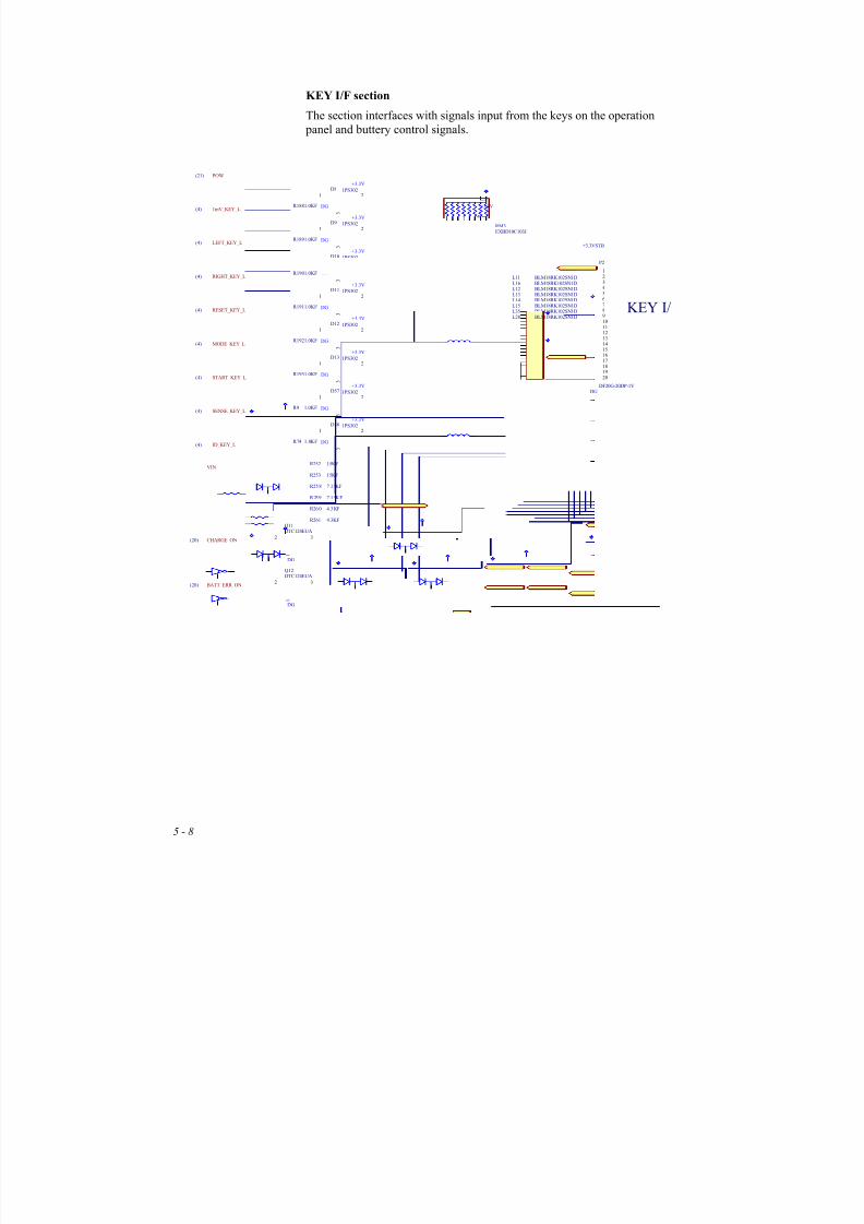
8/13/2019 Manual de Service Fcp-7101 - Fx-7102
http://slidepdf.com/reader/full/manual-de-service-fcp-7101-fx-7102 82/170
5 - 8
KEY I/F section
The section interfaces with signals input from the keys on the operation
panel and buttery control signals.
DG
1
2 1 0 3 9
6
8 4 7 5
RM3EXBD10C103J
+3.3V
POW
1mV_KEY_L
LEFT_KEY_L
RIGHT_KEY_L
RESET_KEY_L
MODE_KEY_L
START_KEY_L
KEY I/
L10 BLM18RK102SN1DL11 BLM18RK102SN1D
L12 BLM18RK102SN1DL13 BLM18RK102SN1D
L14 BLM18RK102SN1DL15 BLM18RK102SN1D
L16 BLM18RK102SN1D
CHARGE_ON
VIN
BATT_ERR_ON
DG
DG
R1881.0KF
R1891.0KF
R1901.0KF
R1911.0KF
R1921.0KF
R1931.0KF
3
21
D8 1PS302
+3.3V
DG
3
21
D9 1PS302
+3.3V
DG
3
21
D10 1PS302
+3.3V
DG
3
21
D11 1PS302
+3.3V
DG
3
21
D12 1PS302
+3.3V
DG
3
21
D13 1PS302
+3.3V
DG
R252 15KF
R253 15KF
R 258 7 .15KF
R259 7.15KF
R260 4 .3KF
R 261 4.3KF
2 3
1
Q11DTC124EUA
2 3
1
Q12DTC124EUA
+3.3VSTB
L35 BLM18RK102SN1D
R9 1.0KF
3
21
D57 1PS302
+3.3V
DGSENSE_KEY_L
(4)
(20)
(20)
(21)
R74 1.0KF
3
21
D58 1PS302
+3.3V
DGID_KEY_L(4)
L28 BLM18RK102SN1D
(4)
(4)
(4)
(4)
(4)
(4)
1234567891011121314151617181920
P2
DF20G-20DP-1V

8/13/2019 Manual de Service Fcp-7101 - Fx-7102
http://slidepdf.com/reader/full/manual-de-service-fcp-7101-fx-7102 83/170
Electric Circuit Diagrams
5 - 9
Thermal head control section
The thermal head control section outputs thermal head signals from the
FPGA to the thermal head. A buffer for level conversion and R and L are
connected as filters to each signal line. The section is also provided with acircuit that generates overheat detection signals to prevent overheating of
the thermal head.
THERMAL I/F
DG
+5V
TDOTCLK
LATCH_L
THM_DATA
STRB
GND
GNDGND
COMCOM
COM
SI
GND
TMSTROBE1*STROBE2*
VDD
COM
CLOCK LATCH*
DG
(+5V)
(+5V)
(+5V)
THERMAL_TEMP
OVH_L
3
21
8
4
IC15A
LM2904PWR
5
67
8
4
IC15B
LM2904PWR
DG
DG
DG
DGDG
+3.3V
+5V+5V
3
21
D141PS302
R2351.0MF
R8220KF
R2627.5KF
C590.1uFFZ
C600.1uFFZ
L18BLM18RK102SN1D
L19BLM18RK102SN1D
L20BLM18RK102SN1D
L21BLM18RK102SN1D
+5V
R2 48 2 2F
R2 49 2 2F
R2 50 2 2F
R2 51 2 2F
2 18
1
2 0
1 0
IC20A
HD74ACT244
4 16
1
2 0
1 0
IC20B
HD74ACT244
6 14
1
2 0
1 0
IC20C
HD74ACT244
8 12
1
2
0
1 0
IC20D
HD74ACT244
R2310KF
R2410KF
R8320KF
+5V
DG
+2.5V
+1.25V
123456789101112131415
P3
DF13B-15P-1.25V(21)
R2510KF
R2610KF
R2710KF
R2810KF
+3.3V
+3.3V
+3.3V
+3.3V
+24V_THERMAL
(5)
(5)
(5)
(5)
(4)
(5)
C2960.1U 50V(1608)
3
2
1
D22
1PS302
+5V
DG

8/13/2019 Manual de Service Fcp-7101 - Fx-7102
http://slidepdf.com/reader/full/manual-de-service-fcp-7101-fx-7102 84/170
5 - 10
Real time clock
The RTC-4574SAA equipped with a 32.768-kHz crystal oscillator is used
as a device for the real time clock. The real time clock operates with a
lithium battery (BT1). If a lithium battery is not mounted, the clock does
not operate.
RESET_LCE1
13
CLK 11
DATA12
FOUT2
FCON14
AIRQ9
VDD7
GND11
TIRQ10
NC3
NC4
NC5
NC6
CE08
IC13
RTC-4574SAA
RTCCE
RTCCLK
RTCDAT
C580.1uFFZ
DG
DG
220mAh
+3.3V
LITIUM_V
3
21
D71PS302
DG
+3.3VA+5V
DG
R223100F
R2341.0MF
3
21
8
4
IC14A
LM2904PWR
12
BT1
CR-2032(VERTICAL)
R2072.0KF
5
67
8
4
IC14B
LM2904PWR
+5V
DG
(4)
(3,4,5,6,21)(4)
(4)
(4)
1 2
D2
SL03
1
2
D16
SL03
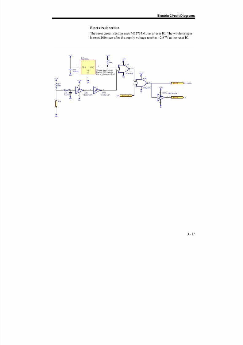
8/13/2019 Manual de Service Fcp-7101 - Fx-7102
http://slidepdf.com/reader/full/manual-de-service-fcp-7101-fx-7102 85/170
Electric Circuit Diagrams
5 - 11
Reset circuit section
The reset circuit section uses M62733ML as a reset IC. The whole system
is reset 100msec after the supply voltage reaches +2.87V at the reset IC.
DG
R410KF
+3.3V
C440.1uFFZ
+3.3V
DG
RESET_L
RESETSW_L
DG
電源が+2.87VになっLレベルで100msecの
VOUT3
G N D
2
VDD1
IC4M62733ML
1 7
8
4
IC5A
74HC3G14DP
+3.3V
R7 10KF
R187
1.0KF
C450.1uFFZ
DG
3 5
IC5B
74HC3G14DP
+3.3V
DG
+3.3V
DG
+3.3V
DG
+3.3V
DG
RESET
13
2
1 4
7
IC6A
74HC08PW
46
5
1 4
7
IC6B
74HC08PW
1 7
8
4
IC18A 74HC3G14DP
(7)
(4,5,6,8,21)
(10)
JP36
When the supply voltageReaches +2.8V, cause the
delay of 100msec at L level.
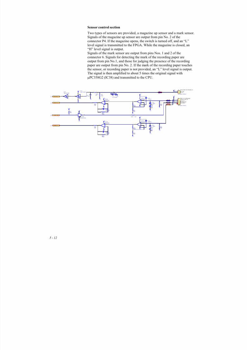
8/13/2019 Manual de Service Fcp-7101 - Fx-7102
http://slidepdf.com/reader/full/manual-de-service-fcp-7101-fx-7102 86/170
5 - 12
Sensor control section
Two types of sensors are provided, a magazine up sensor and a mark sensor.
Signals of the magazine up sensor are output from pin No. 2 of the
connector P4. If the magazine opens, the switch is turned off, and an “L”
level signal is transmitted to the FPGA. While the magazine is closed, an
“H” level signal is output.
Signals of the mark sensor are output from pins Nos. 1 and 2 of the
connector 6. Signals for detecting the mark of the recording paper are
output from pin No.1, and those for judging the presence of the recording
paper are output from pin No. 2. If the mark of the recording paper touches
the sensor, or recording paper is not provided, an “L” level signal is output.
The signal is then amplified to about 5 times the original signal with
µPC358G2 (IC38) and transmitted to the CPU.
マガジンアップセンサCN
SW-ONSW-COM
SENSOR-COM
MARK-E
LED_DRIVE
MARK_DRV_L
HEADUP_L
MARK_V
DG DG
+5V
+3.3V
DG
DGDG
R2 38 51 0F
R239510FC61
0.1uFFZ
R29
10KF
+3.3V
DETECT-E
DETECT_V
+3.3V
DG
12
P4
DF13B-2P-1.25V(21)
マーク/記録紙検出センサCN
11 9
1 9
2 0
1 0
IC20E
HD74ACT244
+5V
DG
12345
P6
DF13B-5P-1.25V(21)
R22410KF
DG
3
2
1
D151PS302
3
21
8
4
IC16A
LM2904PWR
R274100KF
R29124KF
5
67
8
4
IC16B
LM2904PWR
R275100KF
R225100F
C184470pFCHJ
C630.1uFFZ
+3.3V
DG
DGDG
+3.3V
DG
R22610KF
DG
3
2
1
D171PS302
3
21
8
4
IC17A
LM2904PWR
R276100KF
R29224KF
5
67
8
4
IC17B
LM2904PWR
R277100KF
R227100F
C185470pFCHJ
C640.1uFFZ
R3410KF
+3.3V
62
IC5C
74HC3G14DP
JP5
0F
JP6 0F
JP7 0F
JP8 0F(4)
(5)
(4,5)
(4)
17
8
4
IC2A
74HC3G14DP
+3.3V
DG
3
2 1
D18 1PS302
DG
+3.3V
MAGAZINE UP SENSOR CN
Mark on recording paperdetection senor CN
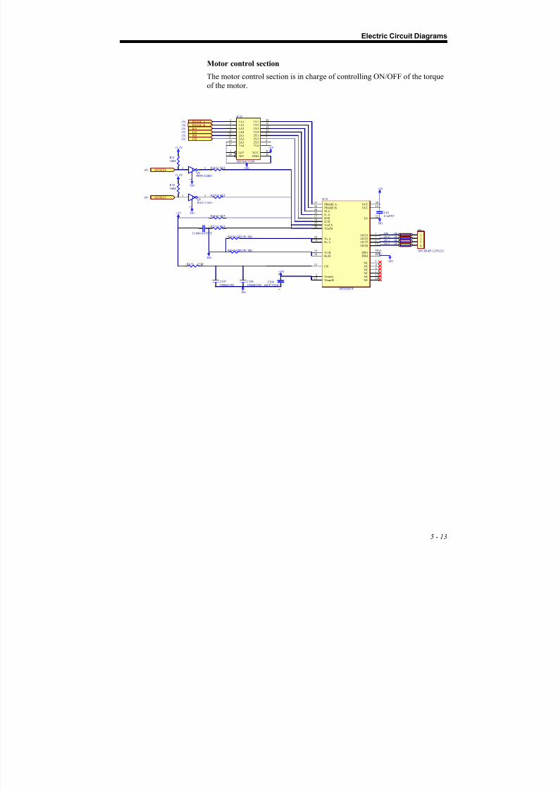
8/13/2019 Manual de Service Fcp-7101 - Fx-7102
http://slidepdf.com/reader/full/manual-de-service-fcp-7101-fx-7102 87/170
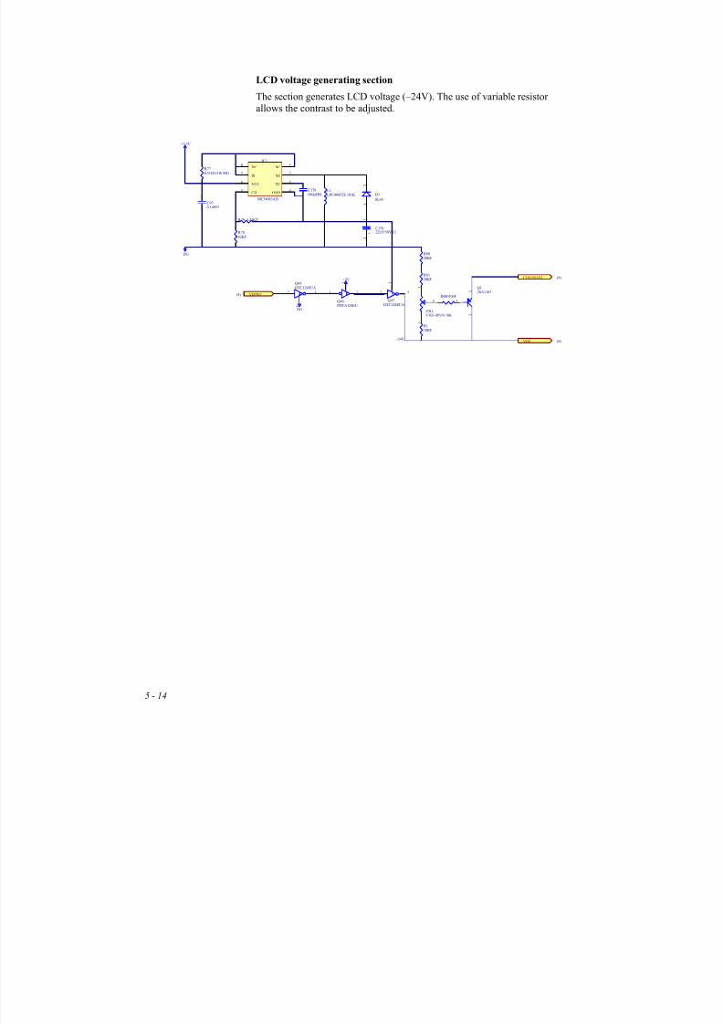
8/13/2019 Manual de Service Fcp-7101 - Fx-7102
http://slidepdf.com/reader/full/manual-de-service-fcp-7101-fx-7102 88/170
5 - 14
LCD voltage generating section
The section generates LCD voltage (–24V). The use of variable resistor
allows the contrast to be adjusted.
1
2
D1
SL03
CONTRAST
3
1
2
VR1V105-4PVN 10K
VEE
R110KF
SC1
SE2
TC3
VCC6
CII5
IS7
GND4
DC8
IC1
MC34063AD
R770.51F(0.5W SR)
R7862KF
R79 3.24KF
C178680pFBJ
L1LPC4045TE 101K
-24V
R8020KF
R8120KF
2
1
+C17922UF/50V(C)
1
2
3
Q12SA1163
+3.3V
DG
VEPWC R480100F
(8)
(8)
(4)2 3
1
Q45DTC124EUA
DG
1 3
2
Q46PDTA124EU
+5V
2 3
1
Q47DTC124EUA
C930.1uFFZ

8/13/2019 Manual de Service Fcp-7101 - Fx-7102
http://slidepdf.com/reader/full/manual-de-service-fcp-7101-fx-7102 89/170
Electric Circuit Diagrams
5 - 15
2. ECG AMP block
The following is a block diagram of ECG AMP.
ECG signals input from patient connectors go through the input protection
section and enter the first-stage amplifier (differential amplifier), where
each signal for right arm, left arm, and chest 1 to chest 6 undergoes
differential amplification with a signal for left leg.Each of the output of the first-stage amplifier is input to the second-stage
amplifier, signals are then switched sequentially with the multiplexer, and
converted to digital signals with the A/D converter.
The digitized ECG signals are then transferred to the CPU with the FPGA.
The ECG AMP block is electrically isolated by a photocoupler and an
isolation power supply.
DC
CPLD
Photo-
coupler
Pulse
trans-
former
Power
voltage
Generating
section
Patient
connectorMulti-
plexer
First-stage amplifier Second-stage amplifier
R
L
C1
C2
C3
C4
C5
C6
F
RF

8/13/2019 Manual de Service Fcp-7101 - Fx-7102
http://slidepdf.com/reader/full/manual-de-service-fcp-7101-fx-7102 90/170
5 - 16
3. Power supply block
The following is a block diagram of the power supply block.
Charger(CV/CC)
Ni-MHBATTERY
(9.6V)(3700mAh)
AC90~264V
47~63Hz
POWERCONTROL
Power controlsignal
DC-DCconverter
+24VDC-DCconverter
+3.3V
+5V
DC-DCconverter
+5.0V
+3.3V
DC-DCconverter
+1.8V
+1.8V
INLET
AC
Adapter
+18V
+3.3V
+5V
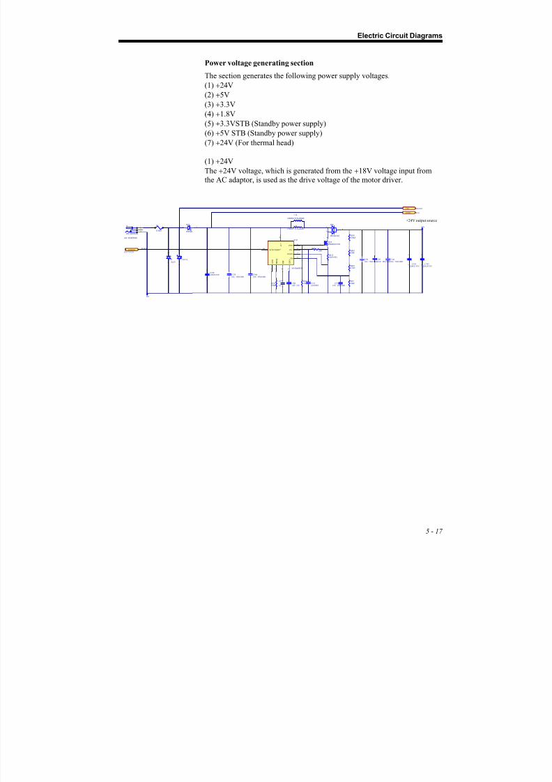
8/13/2019 Manual de Service Fcp-7101 - Fx-7102
http://slidepdf.com/reader/full/manual-de-service-fcp-7101-fx-7102 91/170
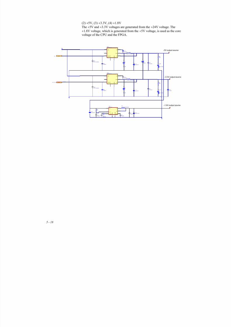
8/13/2019 Manual de Service Fcp-7101 - Fx-7102
http://slidepdf.com/reader/full/manual-de-service-fcp-7101-fx-7102 92/170
5 - 18
(2) +5V, (3) +3.3V, (4) +1.8V
The +5V and +3.3V voltages are generated from the +24V voltage. The
+1.8V voltage, which is generated from the +5V voltage, is used as the core
voltage of the CPU and the FPGA.
C680.1uFFZ
C1530.01UFFZ
1
2
D29
D3FS4A
5VON
C690.1uFFZ
C1540.01UFFZ
1
2
D30
D3FS4A
POWON
1
2
D31
D3FS4A 1
2
LED4
SML-210MT
1
2
LED5
SML-210MT
G N D
3
LX7
IN8
VCC1
FB4
COMP5
P G N D
6
REF2
IC45MAX1952
R6210F
2
1
+ C31333uF/10V(C)
C700.1uFFZ
R414
68KF
C316220pFCHJ
C710.1uFFZ
2
1
+ C317220uF/6.3V(C)C72
0.1uFFZ
C2810.1U 50V(1608)
C2820.1U 50V(1608)
L32
CDRH2D18/HP-2R2NC
L27
CDRH127/LD-680MC
L33
CDRH127/LD-820MC
R4063.3KF
R4181.5KF
VSW8
*
2
G N D
6
CB1
FB4
VIN7
ON/OFF*5
*3
IC46LM2674M-3.3
VSW8
*
2
G N D
6
CB1
FB4
VIN7
ON/OFF*5
*3
IC47LM2674M-5.0
3.3VON
+5V
+3.3V
+1.8V
+5Vの出力元
+3.3Vの出力元
+1.8Vの出力元
+24V
(19)
(13,17,19,21)
2
1
+ C311220UF/35V
2
1
+ C312220UF/35V
C2950.1uFFZ
DG
DG
C390.01UFFZ
C400.01UFFZ
+5V output source
+3.3V output source
+1.8V output source

8/13/2019 Manual de Service Fcp-7101 - Fx-7102
http://slidepdf.com/reader/full/manual-de-service-fcp-7101-fx-7102 93/170
Electric Circuit Diagrams
5 - 19
(5) +3.3VSTB (Standby power supply)
The +3.3V standby power supply used when the DC plug or battery is
connected is generated from the +24V voltage or the battery pack voltage.
The +3.3VSTB is supplied for the IC of the power supply block.
(6) +5V STB (Standby power supply)
The +5V standby power supply used when the DC plug is connected is
generated from the +18V voltage. The +5VSTB is supplied for the IC of the
power supply block.
IN3
OUT1
G N D
2
IC43 NJM78L05UA
C1520.01UFFZ
2
1
+ C31033uF/10V(C)
R5710KF
CHGENA
C650.1uFFZ
R20 8 2 .0 KF
C660.1uFFZ
R5812KF
R5912KF
R384 47KF
C2001000pFCHJ
R1951.0KF
C670.1uFFZ
C2011000pFCHJ
R41351KF
JP340F
R2124.7KF
R2134.7KF
R6010KF
R6110KF
R228100F
R396150KF
JP350F
VTEMP
CHGSTS
VBAT(M)
R4202.7KF
R4213.3KF
R423
330KF
R424
330KF
R425
0.12F(1WNPR)
C2861.0U 25V
3 1
2D341PS184
C3054.7UF(50V)
I N H *
1 6
L E D 2
1 1
TS7
BAT8
MOD14
TCO6
TM14
VCC13
VSS12
DSEL2
DCMD*1
SNS9
L E D 1
1 0
TM25
DIS15
VSEL3
IC44
BQ2004ESN
1 3
2
Q42PDTA124EU
1 3
2
Q29PDTC124EU
1
3
D27
BZX84-B5V6
3
2
1
Q412SK2112
(17)
(20)
(13)
(13,16)
DG
+5VSTB
CHARGE
(7) +24V (For thermal head)
The +24V power supply voltage exclusive for the thermal head is generated.
A circuit for prevention of overcurrent is provided.
1
32
Q92SC2873
1
23
Q44 2PC4081
14D43A
BAS28
23D43B
BAS28
14D44A
BAS28
23D44B
BAS28
14D45A
BAS28
23D45B
BAS28
1 4D46A
BAS28
23D46B
BAS28
R283
100KF
R229 100F
V S S
2
C D
3
VOUT1
VOR 4
VIN5
IC62S-873325BUP-ALA
C1560.01UFFZ
C1570.01UFFZ
VBAT(P) 2
1
+ C31433uF/10V(C)
C3074.7UF(50V)
1 3
2
Q43PDTA124EU
1 3
2
Q34PDTC124EU
DG
+3.3VSTB
+3.3VSTBの出力元
+24V
1 2
D47
SL03(13,14,16)
C2970.1U 50V(1608)
C2980.1U 50V(1608)
+3.3VSTB output source
R4372.2KF
R38747KF
R38810KF
R38915KF
R407 220KF
R39015KF
R4382.2KF
R6810KF
THRMON
R440
1.0F(1W)
C2830.1U 50V(1608)
2
1
+
C3201500UF/35V(C)
2
1
+
C3211500UF/35V(C)
R4414.7KF
1
43
Q402SJ529
C309
4.7UF(50V)
+24V +24V_THERMAL
(20) 1 3
2
Q3PDTC124EU
1 3
2
Q7PDTC124EU
1 3
2
Q26PDTC124EU
1
2
3
Q22SA1163
R662.2KF
R6747KF
5
6
7
8
4
IC51B
LM2904PWR
+24V
R391220KF
DG
DG
R4462KF(1WNPR)
JP1980F
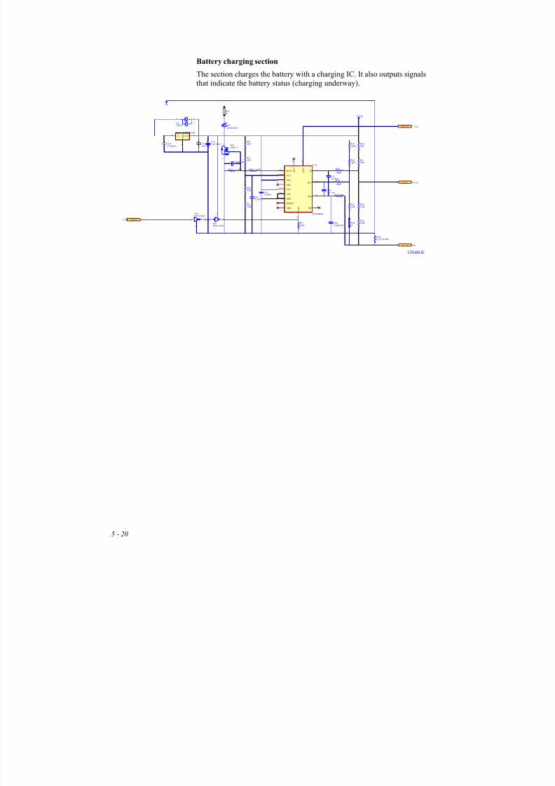
8/13/2019 Manual de Service Fcp-7101 - Fx-7102
http://slidepdf.com/reader/full/manual-de-service-fcp-7101-fx-7102 94/170
5 - 20
Battery charging section
The section charges the battery with a charging IC. It also outputs signals
that indicate the battery status (charging underway).
IN3
OUT1
G N D
2
IC43 NJM78L05UA
C1520.01UFFZ
2
1
+ C31033uF/10V(C)
R5710KF
CHGENA
C65
0.1uFFZ
R20 8 2 .0 KF
C660.1uFFZ
R5812KF
R5912KF
R384 47KF
C2001000pFCHJ
R1951.0KF
C670.1uFFZ
C2011000pFCHJ
R41351KF
JP340F
R2124.7KF
R2134.7KF
R6010KF
R6110KF
R228100F
R396150KF
JP350F
VTEMP
CHGSTS
VBAT(M)
R4202.7KF
R4213.3KF
R423
330KF
R424
330KF
R4250.12F(1WNPR)
C2861.0U 25V
3 1
2D341PS184
C3054.7UF(50V)
I N H *
1 6
L E D 2
1 1
TS7
BAT8
MOD14
TCO6
TM14
VCC13
VSS12
DSEL2
DCMD*1
SNS9
L E D 1
1 0
TM25
DIS15
VSEL3
IC44
BQ2004ESN
1 3
2
Q42PDTA124EU
1 3
2
Q29PDTC124EU
1
3
D27
BZX84-B5V6
3
2
1
Q412SK2112
(17)
(20)
(13)
(13,16)
DG
+5VSTB
CHARGE

8/13/2019 Manual de Service Fcp-7101 - Fx-7102
http://slidepdf.com/reader/full/manual-de-service-fcp-7101-fx-7102 95/170
Electric Circuit Diagrams
5 - 21
Power control section
The section monitors the temperature and the voltage of the battery, and
transmits the status with various signals.
R415150KF
R397150KF
25
4
IC48A
LM339PWR
R398150KFC73
0.1uFFZ
R25415KF
R280100KF
R6310KF
[1.017V]
VTEMPBAT>=70_L
17
6
IC48B
LM339PWR
R428470KF
R429470KF
R26822KF
VBAT(P)
R399150KF
R281100KF C74
0.1uFFZ
R400150KF
R41668KF
R2164.7KF
R6410KF
VIN
BAT>=14.4V_L
VBATOP
R430470KF
R25515KF
R393220KF
R38547KF
R282100KF C75
0.1uFFZ
C1550.01UFFZ
ACDET
2
3
1
IC50UPC1093T
R433620F
C2031000pFCHJ
149
8
IC48C
LM339PWR
R6510KF
3
1 2
D371PS184
C3064.7UF(50V)
BATT_VOL
BATT_TMP
DG
+5VSTB
(17,20)
(17)
(17)
(4)
(4)
(13,14,18)
(19)
(8,13,18)
(13,14)
3
21
8
4
IC49A
LM2904PWR
5
67
8
4
IC49B
LM2904PWR
+5VSTB
+5VSTB
C770.1uFFZ
13
11
10
IC48D
LM339PWR
R7010KFR127
150KF
R71150KFC97
0.1uFFZ
R1283.9KF
R12939KF
BAT<=8V_L (17)
DG
DG
R336 4.7KF
AC/DC STATUS
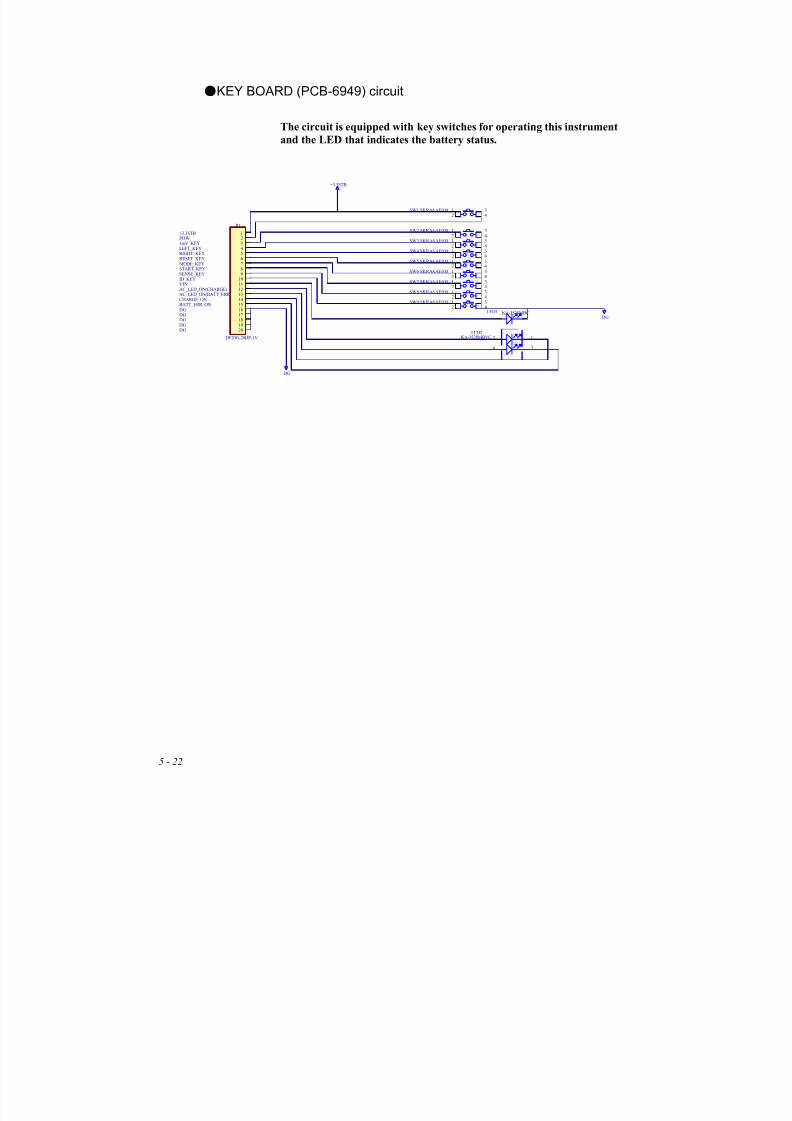
8/13/2019 Manual de Service Fcp-7101 - Fx-7102
http://slidepdf.com/reader/full/manual-de-service-fcp-7101-fx-7102 96/170
5 - 22
KEY BOARD (PCB-6949) circuit
The circuit is equipped with key switches for operating this instrument
and the LED that indicates the battery status.
12
34
SW1 SKRAAAE010
POW1mV_KEYLEFT_KEYRIGHT_KEYRESET_KEYMODE_KEYSTART_KEY
VIN
CHARGE_ONBATT_ERR_ON
AC_LED_ON(CHARGE)AC_LED_ON(BATT_ERR)
+3.3STB
DG
+3.3STB
DG
12
34
SW2 SKRAAAE010
12
34
SW3 SKRAAAE010
12
34
SW4 SKRAAAE010
12
34
SW5 SKRAAAE010
1
2
3
4
SW6 SKRAAAE010
12
34
SW7 SKRAAAE010
DG
SENSE_KEY
12
34
SW8 SKRAAAE010
LED1 KA-3528MBC
2 1
4 3
LED2KA-3528MBYC
ID_KEY
12
34
SW9 SKRAAAE010
DGDGDGDG
123456789
1011121314151617181920
P1
DF20G-20DP-1V
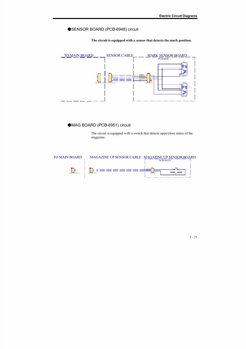
8/13/2019 Manual de Service Fcp-7101 - Fx-7102
http://slidepdf.com/reader/full/manual-de-service-fcp-7101-fx-7102 97/170

8/13/2019 Manual de Service Fcp-7101 - Fx-7102
http://slidepdf.com/reader/full/manual-de-service-fcp-7101-fx-7102 98/170
5 - 24
AC adaptor block diagram
The following is a block diagram of the AC adaptor.
The input of the AC adaptor is worldwide capable, allowing 90V to 264VAC to be input. The +18V voltage generated with the AC adaptor is
supplied to this instrument with a power jack.
INLET
FUSE
FUSE
Line Filter
Rush currentprotect circuit
+18V
Main circuit
Main SWcontrol circuit
Power jack
+
Feedbackcircuit
AC90~264V
47~63Hz
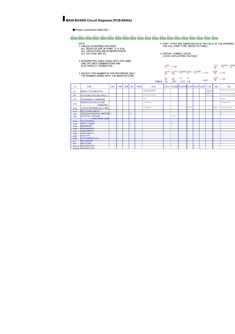
8/13/2019 Manual de Service Fcp-7101 - Fx-7102
http://slidepdf.com/reader/full/manual-de-service-fcp-7101-fx-7102 99/170
MAIN BOARD Circuit Diagrams (PCB-6950A)
Power connection table No.1
MAIN02MAIN02.SCH
MAIN03MAIN03.SCH
MAIN04MAIN04.SCH
MAIN05MAIN05.SCH
MAIN06MAIN06.SCH
MAIN07MAIN07.SCH
MAIN08MAIN08.SCH
MAIN09MAIN09.SCH
MAIN10MAIN10.SCH
ECG11ECG11.SCH
ECG12ECG12.SCH
POW13POW13.SCH
POW14POW14.SCH
POW15POW15.SCH
POW16POW16.SCH
POW17POW17.SCH
POW18POW18.SCH
POW19POW19
NOTE
1. UNLESS OTHERWISE SPECIFIED
ALL RESISTOR ARE IN OHMS. ±1% 0.1W
ALL CAPACITORS ARE IN MICROFARADS.
ALL VOLTAGE ARE DC.
2. INTERRUPTED LINES CODED WITH THE SAME
LINE OR LINES COMBINATIONS ARE
ELECTRICALLY CONNECTED.
3. DEVICE TYPE NUMBER IS FOR REFERENCE ONLY.
THE NUMBER VARIES WITH THE MANUFACTURE.
4. PART TYPES ARE ABBREVIATED I
FOR FULL PART TYPE, REFER TO
5. SPECIAL SYMBOL USAGE.
±5VA=±5FLOATING VALTAGE.
DG
TABLE
+3.3V
HD6417727F100C(CPU)IC7
IC8
+3.3VA
IC TYPE +5V +3.3V
UPD45128163G5-A75-9JFIC12
TE28F640J3C-120(FROM)IC11
(SDRAM)
DGF
RTC-4574SAA(RTC)IC13
MTD2007F(MOTOR_DRIVER)
XC2S100E-6TQ144C(FPGA)
IC55 LAN91C96TQFP(LAN_CTRL)
+2.5VF+24V +3.3VA +3.3VDF +3.3VSTB+5VDF -VTRF
20,31,44,55,66,77,88,102,117,134,161,190,209,225,231
237
17,36,53,72,90,108,128,144
9,37,43
1,3,9,14,27,43,49
11,19,38,48,59,98
+3.3VL
71,79,89
7
IC21 15,28 2,13
XC9572XL-10VQ44CIC38
(CPLD FOR AMP)
15,26,35
TLC3541DGK IC37 6 3
TPS77133DGK IC39 7,85,6
BQ2004ESNIC44 13
+18V
MAX668EUBIC42 9
LM2674M-5.0IC47 7
LM2674M-3.3IC46 7
MAX1952IC45 8
S-873325BUP-ALAIC62 5
MC34063ADIC1 6
M62733MLIC4 1
MAX4521CEEIC31,32 13 4
MAX4051CEEIC28,29 16 7
+24V= +24V
+3.3STB+3.3VL
-2.5VF AGL
+3.3VDF
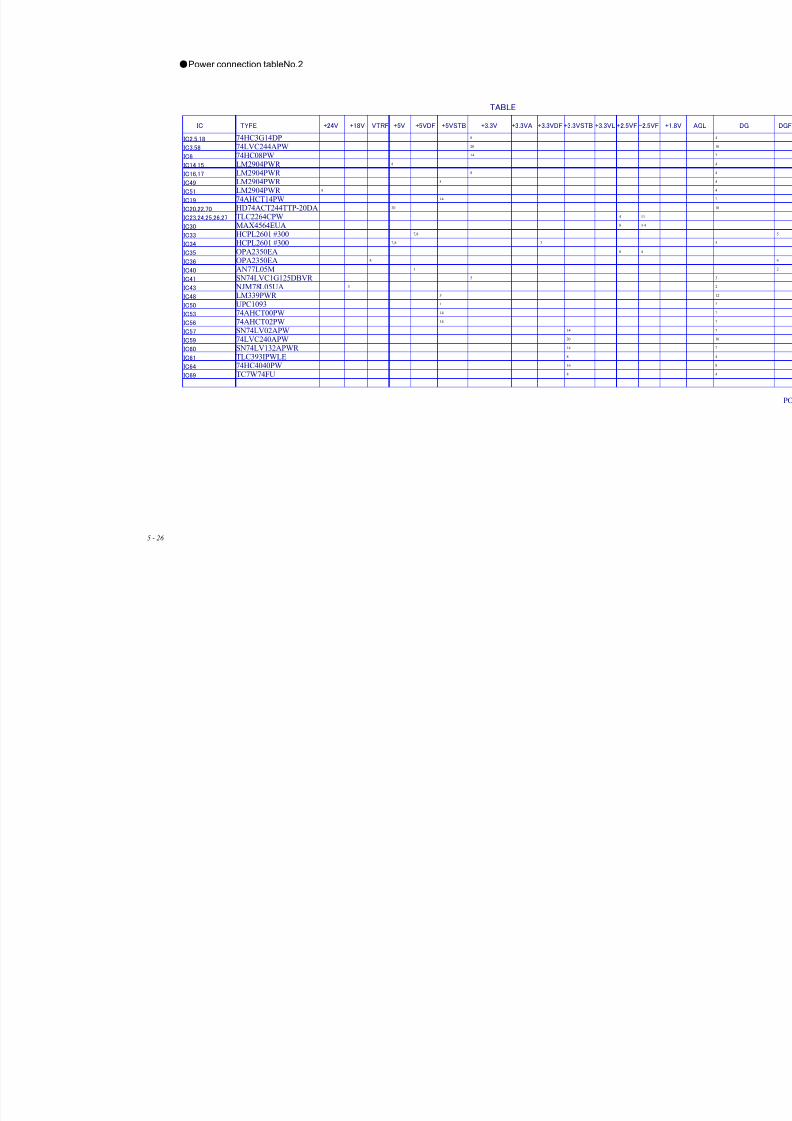
8/13/2019 Manual de Service Fcp-7101 - Fx-7102
http://slidepdf.com/reader/full/manual-de-service-fcp-7101-fx-7102 100/170
5 - 26
Power connection tableNo.2
TABLE
74HC3G14DPIC2,5,18
IC3,58
IC TYPE +5V +1.+3.3V
LM2904PWR IC14,15
74HC08PWIC6
HD74ACT244TTP-20DAIC20,22,70
74LVC244APW
IC19 74AHCT14PW
+2.5VF+24V +3.3VA +3.3VDF +3.3VSTB+5VDF -2.5VF VTRF
8
20
14
8
14
+3.3VL
20
+18V
IC16,17
8
IC49
IC51
8
8
TLC2264CPWIC23,24,25,26,27 4 11
MAX4564EUAIC30 8 3,4
HCPL2601 #300IC33 7,8
HCPL2601 #300IC34 7,8 2
OPA2350EAIC35
OPA2350EAIC36
8 4
8
AN77L05MIC40 1
SN74LVC1G125DBVR IC41 5
NJM78L05UAIC43 3
LM339PWR IC48 3
UPC1093IC50 1
74AHCT00PWIC53 14
74AHCT02PWIC56 14
IC57 14
74LVC240APWIC59 20
SN74LV132APWR IC60 14
TLC393IPWLEIC61 8
74HC4040PWIC64 16
TC7W74FUIC69 8
+5VSTB
LM2904PWR
LM2904PWR
LM2904PWR
SN74LV02APW
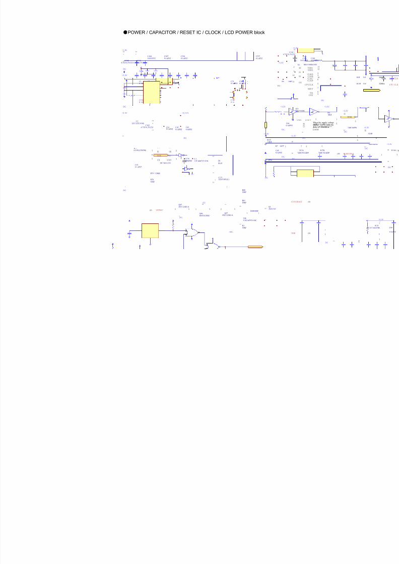
8/13/2019 Manual de Service Fcp-7101 - Fx-7102
http://slidepdf.com/reader/full/manual-de-service-fcp-7101-fx-7102 101/170
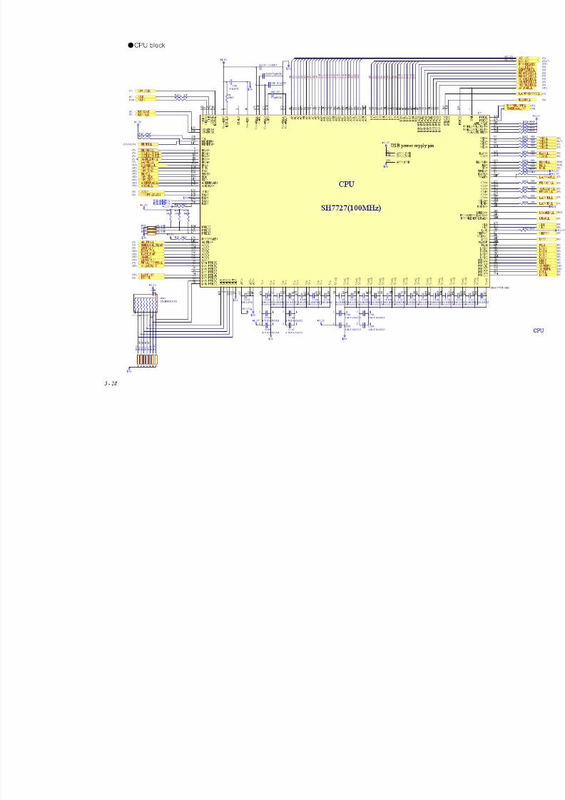
8/13/2019 Manual de Service Fcp-7101 - Fx-7102
http://slidepdf.com/reader/full/manual-de-service-fcp-7101-fx-7102 102/170
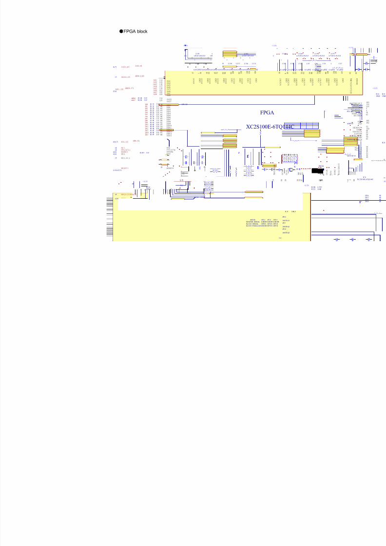
8/13/2019 Manual de Service Fcp-7101 - Fx-7102
http://slidepdf.com/reader/full/manual-de-service-fcp-7101-fx-7102 103/170

8/13/2019 Manual de Service Fcp-7101 - Fx-7102
http://slidepdf.com/reader/full/manual-de-service-fcp-7101-fx-7102 104/170
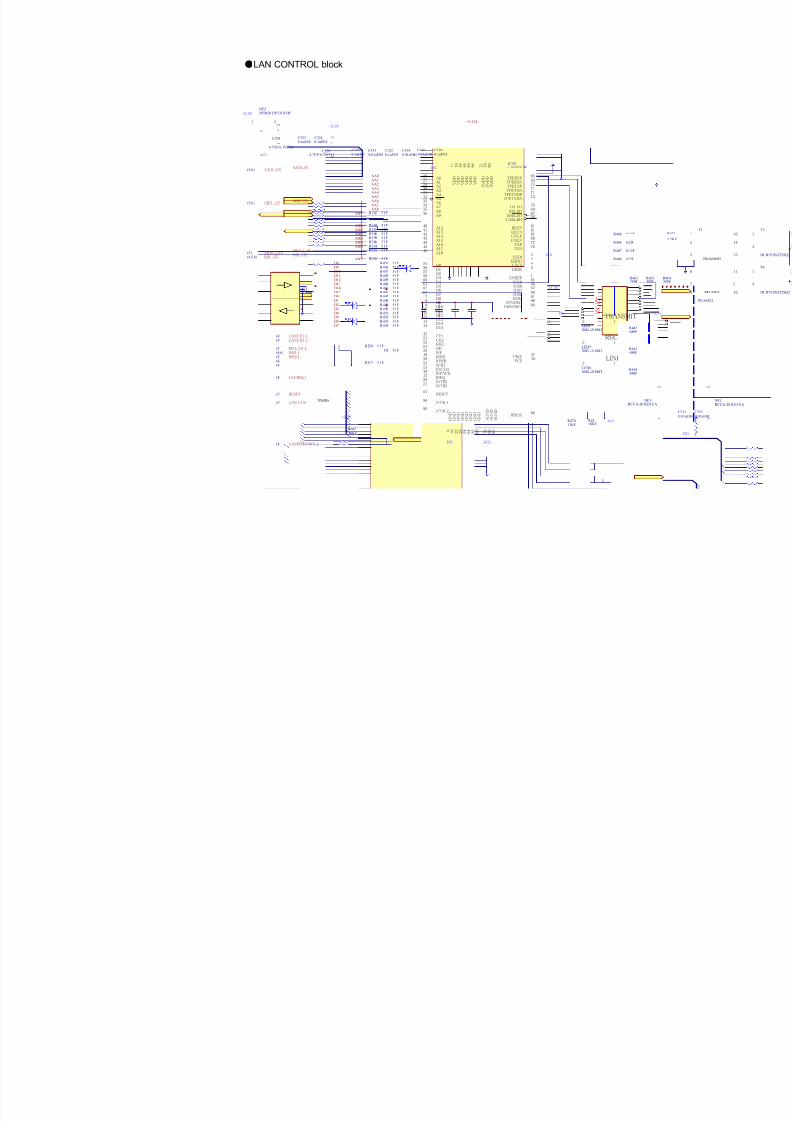
8/13/2019 Manual de Service Fcp-7101 - Fx-7102
http://slidepdf.com/reader/full/manual-de-service-fcp-7101-fx-7102 105/170
LAN CONTROL block
D[0..15]
LANWAIT_LWR3_LWR2_LWR1_L
LANCE1_LLANCE2_L
AA[0..8]
D[0..15]
DG AGL
AGL
DG
LANPWDOWN_L
+3.3V
LANIRQ_L
+3.3V
TRANSMIT
RECEIVE
LINK
A026
A127
A1543
A228
A330
A431
A532
A633
A734
A835
A936
FWE 37
FCS 39
A1240
A1341
A1442
A1644
A1745
A1846
CE147
D055
D156
D257
D358D4
60
D561
D662
D763
D87
D98
D109
D1110
D1212
D1313
D1414
D1515
XTAL194
XTAL295
V D D
1 9
V D D
3 8
V D D
4 8
V D D
5 9
V D D
9 8
V D D
1 1
A V D D
7 1
A V D D
7 9
A V D D
8 9
G N D
1 0 0
G N D
6
G N D
1 6
G N D
2 2
G N D
2 9
G N D
5 4
G N D
6 4
G N D
9 2
A G N D
7 8
A G N D
8 6
A G N D
8 7
RBIAS 88
TPERXP 85
TPERXN 84
TPETXP 75
TPETXN 73
TPETXDP 72
TPETXDN 74
EEDI 3
EEDO 2
EECS 4
EESK 5
PWRDWN 66
XENDEC 90
EN16 91
ROM 93
ENEEP 1
IOS0 96
IOS1 97
IOS2 99
REG52
RESET65
WE25
CE224
OE51
IORD49
IOWR50
WAIT53
IOCS1623
IREQ17
INPACK18
INTR220
INTR321
TXLED 70
RXLED 69
BSELED 67
LNKLED 68
RECP 83
COLP 81
COLN 80
TXP 77
TXN 76
RECN 82
IC55LAN91C96
RESET
+3.3V
+3.3V
AGL
R443680F
R444680F
R445680F
R463300F
R464300F
R465300F
R466 61.9F
R467 61.9F
R468 422F
R469 422F
C3230.1uFFZ
C3240.1uFFZ
C3250.1uFFZ
C3260.1uFFZ
C3300.01uFBJ
1 3
2
NF2 NFM2012P13C474F
C3330.01uFBJ
R2210KF
R47012KF
AGL
R471
1.2K
R472 51F
R447 51FR448 51FR449 51FR450 51FR451 51FR452 51FR453 51FR454 51F
R455 51FR456 51FR457 51F
R458 51FR459 51FR460 51FR461 51FR462 51F
2
1
+
C328
4.7UF/6.3V(T)3
2
1
+
C3294.7UF/6.3V(T)3
C3340.01uFBJ
+3.3VL
DG
C3270.1uFFZ
12LED6SML-210MT
12LED7SML-210MT
12LED8SML-210MT
D0D1D2D3D4D5D6D7
D8D9D10
D11D12D13D14D15
LAN_CLK 20MHz
R44210KF
+3.3V
AA0
1
2
NF3RCCA-201Q31UA
(5,6)
(4,5,6)
(3)
(4)(4)
(4)
(4)
(4)
(3)
(4,6)(4)(4)
AB13AB14AB15
AB23
AA[0..23]
AA2AA3AA4AA5AA6AA7AA8
AA1
AB[1..23] AB[9..23]
AB9
AB10AB11AB12
R182 51F
R184 51FR 185 51FR186 51FR199 51FR206 51FR214 51F
AB16_LAN AB16_LAN R215 51F
R218 51F
RD_LAN_L R220 51F
(5,6)
(5)
(5)
R237 51F
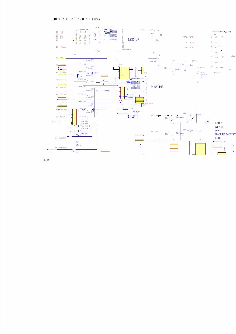
8/13/2019 Manual de Service Fcp-7101 - Fx-7102
http://slidepdf.com/reader/full/manual-de-service-fcp-7101-fx-7102 106/170
5 - 32
LCD I/F / KEY I/F / RTC / LED block
L3 BLM18RK102SN1L4 BLM18RK102SN1
L5 BLM18RK102SN1
L6 BLM18RK102SN1
L7 BLM18RK102SN1L8 BLM18RK102SN1
R2 40 2 2FR2 41 2 2F
R2 42 2 2F
R2 43 2 2F
R2 44 2 2FR245 22F
L9 BLM18RK102SN1R2 46 2 2F
CL1CL2
DONFLM
LCD0LCD1LCD2LCD3
DG
1
2 1 0 3 9
6
8 4 7 5
RM3EXBD10C103J
+3.3V
POW
1mV_KEY_L
LEFT_KEY_L
RIGHT_KEY_L
RESET_KEY_L
MODE_KEY_L
START_KEY_L
LCD I/F
KEY I/F
DG
CONTRAST
L10 BLM18RK102SN1L11 BLM18RK102SN1
L12 BLM18RK102SN1L13 BLM18RK102SN1L14 BLM18RK102SN1L15 BLM18RK102SN1
L16 BLM18RK102SN1
CHARGE_ON
VIN
BATT_ERR_ON
DG
DG
R1881.0KF
R1891.0KF
R1901.0KF
R1911.0KF
R1921.0KF
R1931.0KF
3
21
D8 1PS302
+3.3V
DG
3
21D9 1PS302
+3.3V
DG
3
21
D10 1PS302
+3.3V
DG
3
21D11 1PS302
+3.3V
DG
3
21
D12 1PS302+3.3V
DG
3
21
D13 1PS302
+3.3V
DG
R252 15KF
R253 15KF
R258 7.15KF
R259 7.15KF
R260 4.3KF
R261 4.3KF
2 3
1
Q11DTC124EUA
2 3
1
Q12DTC124EUA
L17 BLM18RK102SN1R2 47 2 2F
+3.3VSTB
12345678
91011121314
P1
00 6207 33 29 14 000
VEE
+5V
RESET_LRTCCE
RTCCLK
RTCDAT
DG
220mAh
+3.3V
LITIUM
3
21
D71PS302
DG
+3.3VA+5V
DG
R223100F
R2341.0MF
3
21
8
4
IC14A
LM2904PWR
12
BT1
CR-2032(VERTICAL)
R2072.0KF
7
8
4
I
L
+5V
DG
DG
1G*1
1A12
2Y4 3
1A24
2Y3 5
1A36
2Y2 7
1A48
VCC 20
2G*19
1Y1 18
2A417
1Y2 16
2A315
1Y3 14
2A213
1Y4 12
2A111
2Y1 9
GND 10
IC70 HD74ACT244
+5V
C3350.1uFFZ
L35 BLM18RK102SN1
R9 1.0KF
3
21D57 1PS302
+3.3V
DGSENSE_KEY_L
(4)
(20)
(20)
(4)(4)
(3)
(4)(4)
(21)
(3,4,5,6,21)(4)
(4)
(4)(3)
(13,16,18)
R74 1.0KF
3
21D58 1PS302
+3.3V
DGID_KEY_L(4)
L28 BLM18RK102SN1
1 2D2
SL03
1
2
D16
SL03
DG
DG
R210KF
LED0 1 2
LED2 SML-210MTR93 680F
DG
R310KF
LED1 1 2
LED3 SML-210MTR94 680F15 5
1 9
IC3G
74LVC244APW
13 7
1 9
IC3F
74LVC244APW
(4)
(4)
(4)
(4)
(4)
(4)
(4)
(4)
(4)(4)
(4)(4)
123
4567891011121314151617181920
P2
DF20G-20DP-1V
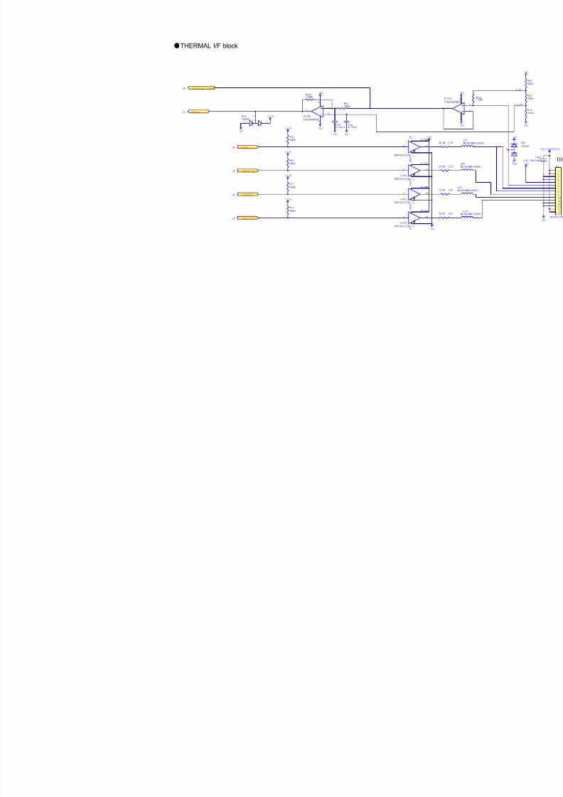
8/13/2019 Manual de Service Fcp-7101 - Fx-7102
http://slidepdf.com/reader/full/manual-de-service-fcp-7101-fx-7102 107/170
THERMAL I/F block
TDOTCLK
LATCH_L
THM_DATA
STRB
DG
(+5V)
(+5V)
(+5V)
THERMAL_TEMP
OVH_L
3
21
8
4
IC15ALM2904PWR
5
67
8
4
IC15B
LM2904PWR
DG
DG
DG
DGDG
+3.3V
+5V+5V
3
21
D141PS302
R235
1.0MF
R8220KF
R27.5
C590.1uFFZ
C600.1uFFZ
L18BLM18RK102SN
L19BLM18RK102SN1
L20BLM18RK102SN
L21BLM18RK102
+5V
R248 22F
R249 22F
R250 22F
R251 22F
2 18
1
2 0
1 0
IC20A
HD74ACT244
4 16
1
2 0
1 0
IC20B
HD74ACT244
6 14
1
2 0
1 0
IC20C
HD74ACT244
8 12
1
2 0
1 0
IC20D
HD74ACT244
R2510KF
R2610KF
R2710KF
R2810KF
+3.3V
+3.3V
+3.3V
+3.3V
(5)
(5)
(5)
(5)
(4)
(5)
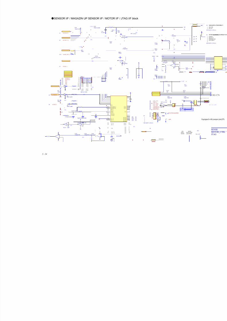
8/13/2019 Manual de Service Fcp-7101 - Fx-7102
http://slidepdf.com/reader/full/manual-de-service-fcp-7101-fx-7102 108/170
5 - 34
SENSOR I/F / MAGAZIN UP SENSOR I/F / MOTOR I/F / JTAG I/F block
MARK_DRV_L
HEADUP_L
MARK_V
DG DG
+3.3V
DG
DGDG
R238 510F
R239510FC61
0.1uFFZ
R29
10KF
NC 1
VCC 28
PHASE A27
I0 A26
I1 A25
Vs A24
Vref A23
LG 22
CR21
Vref B20
Vs B19
I1 B18
I0 B17
PHASE B16
VCC 15
VmmA2
OUT1 3
NC 4
Rs A5
NC 6
OUT2 7
OUT3 8
NC 9
Rs B10
NC 11
OUT4 12
Vmm B13
NC 14
FIN1 FIN1
FIN2 FIN2
IC21
MTD2007F
PHASE_A
PHASE_BI0AI1AI0BI1B
MVREF0
MVREF1
DG
1 3
2
Q5PDTC124EU
1 3
2
Q6PDTC124EU
DG
R3010KF
+3.3V
R3110KF
+3.3V
+5V
DG
C620.1uFFZ
R2650.47F(1W SR)
R2660.47F(1W SR)
DG
R267 22KF
DETECT_V
+3.3V
DG
R2637.5KF
R2703.0KF
R2647.5KF
R2713.0KF
C1480.01UFFZ
+5V
C1971000pFCHJ
C1981000pFCHJ
DG
+24V 2
1
+C204
68UF/35V(C)1
11 9
1 9
2 0
1 0
IC20E
HD74ACT244
+5V
DG
1G*1
1A12
2Y4 3
1A24
2Y3 5
1A36
2Y2 7
1A48
VCC 20
2G*19
1Y1 18
2A417
1Y2 16
2A315
1Y3 14
2A213
1Y4 12
2A111
2Y1 9
GND 10
IC22
HD74ACT244
DG
+5V
RESETSW_L
CPU_TCK
CPU_TMS
TRST_L
CPU_TDI
CPU_TDO
ASEBRKAK_L
ASEMD_L
FROMWR_L
+3.3V
R27268F
R3210KF
C206100pFCHJ
DG
+3.3V
R27368F
R3310KF
C207100pFCHJ
DG
JP31OPENSHORT
MODE
ASE MODEMAIN MODE
FPGA_TCK
FPGA_TMSFPGA_TDI
FPGA_TDO
1
234
P5
DF13B-4P-1.25V(21)
R22410KF
DG
3
2
1
D151PS302
3
2
1
8
4
IC16A
LM2904PWR
R274100KF
R29124KF
5
67
8
4
IC16B
LM2904PWR
R275100KF
R225100F
C184470pFCHJ
C630.1uFFZ
+3.3V
DG
DGDG
+3.3V
DG
R22610KF
DG
3
2
1
D171PS302
3
21
8
4
IC17A
LM2904PWR
R276100KF
R29224KF
5
67
8
4
IC17B
LM2904PWR
R277
100KF
R227100F
C185470pFCHJ
C640.1uFFZ
R3410KF
+3.3V
62
IC5C
74HC3G14DP
JP5
0F
JP9 0FJ P10 0F
J P11 0FJ P12 0F
(4)
(4)
(4)
(4)
(4)(4)
(4)
(5)
(5)
(5)(5)
(6)
(5)
(4,5)
(4)
(4)
(4)
(3)
(4)
DG
(5)
(5)(5)(5)(5)(5)
17
8
4
IC2A
74HC3G14DP
+3.3V
DG
3
2 1
D18 1PS302
DG
+3.3V
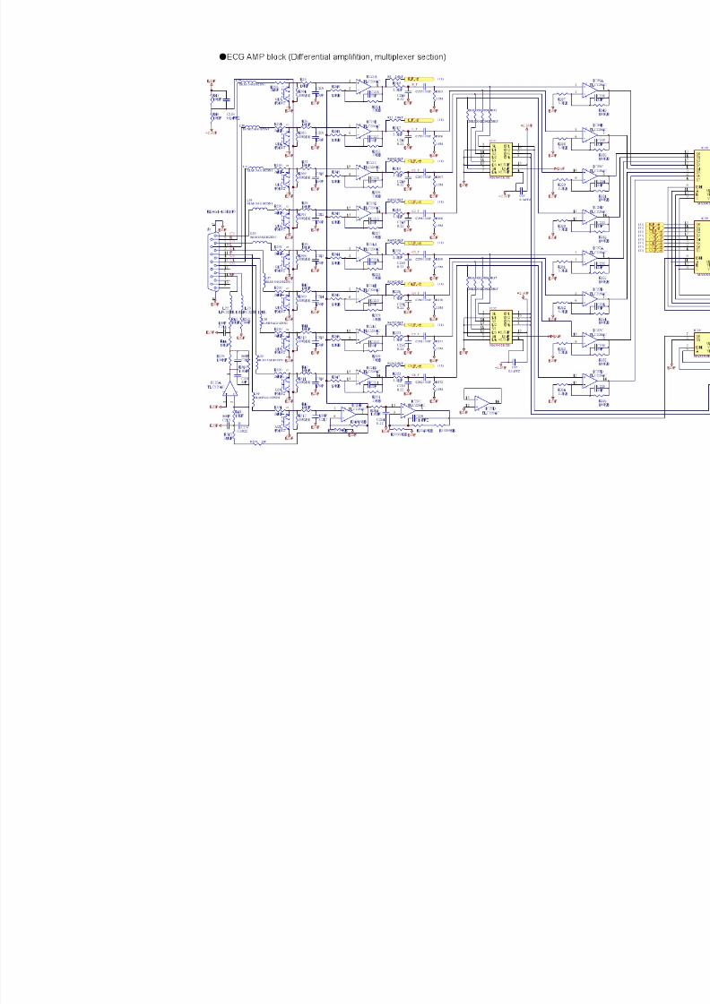
8/13/2019 Manual de Service Fcp-7101 - Fx-7102
http://slidepdf.com/reader/full/manual-de-service-fcp-7101-fx-7102 109/170

8/13/2019 Manual de Service Fcp-7101 - Fx-7102
http://slidepdf.com/reader/full/manual-de-service-fcp-7101-fx-7102 110/170
5 - 36
ECG AMP block (ADC, CPLD and POWER section)
-2.5VF
+2.5VF
6
72
35
8IC34
HCPL2601
+5V
+3.3VDF
+5VDF+5V
2 2
4 4
1 1
3
3
5
5
77
66
88 T1
FT-2155
DGF
+5VDF
+5V
E25F
-2.5VF -2.5VF
3
2
1
Q22
2SK2112
3
2
1
Q232SK2112
3
21
8
4
IC35A
OPA2350EA
5
67
8
4
IC35B
OPA2350EA
R30224KF
R30324KF
R374
1.2KF
R3751.2KF
3
2
1
3
2
1
C2630.01UFF
C2640.01UFF
R3761.2KF
R377510F
C2400.1uFFZ
1
2
D3SL03
1
2
D4SL03
1
2
D5SL03
1
2
D6SL03
C2410.1uFFZ
C2420.1uFFZ
DGF
C2430.1uFFZ
3
2 1
D211PS302 -2.5VF
+2.5VF
R37810F
R37910F 2
1
+ C267
22/4V
-2.5VF
+5VDF
F1TF16N0.50
F2TF16N0.25
REF2 AIN
4
CS* 1
GND3
VDD6
SCLK 5
SDO 8FS
7
IC37
TLC3541DGK
VCCINT 15
VCCINT 35
VCCIO 26
GND 4
GND 17
GND 25
TCK 11
TDI 9
TDO 24
TMS 10
AD_DATA18
AD_CS_L19
INST_033
INST_132
INH_A31
INH_B30
INH_C29
MUX_022
MUX_121
MUX_220
RXD 5
TXD 7
CLK43
RESET_L40
IC38
XC9572XL-10VQ44C
ECG_SIG
INST0_L
INST1_L
INH_AINH_BINH_C
MUX_0MUX_1MUX_2
+3.3VDF
+2.5VF+2.5VF
-2.5VF
C2690.1uFFZ
+3.3VDF
DGF
C270
0.1uFFZ
2
1
+
C27415/16V
2
1
+
C27515/16V
C271
0.1uFFZ
C272
0.1uFFZ
C273
0.1uFFZ
3
21
8
4
IC36AOPA2350EA
5
67
8
4
IC36B
OPA2350EA
OUT8
OUT7
FB/SENCE1
GND 4
IN 5
IN 6
RESET_L2
ENABLE_L 3
IC39TPS77133DGK
+3.3VDF
2
1
+C27615/16V
C2440.1uFFZ
DGF
C2450.1uFFZ
R380330F
R33839KB
R33939KB
-2.5VF
D25
LM4050CIM3-2.5
R381910F
VTRF
IN 3
OUT1
G N D
2
IC40AN77L05M
AMP_FPGA_TCK
AMP_FPGA_TDOAMP_FPGA_TMS
AMP_FPGA_TDI
ジャンパーピン(2P)を実装
R5210KF
R5310KF
R5410KF
+3.3VDF
DG
DGF
VTRF
DGF
-2.5VF
2
1
+
C1754.7UF/6.3V(T)3
2
1
+C195
1.0UF/16V(T)3
2
1
+
C1764.7UF/6.3V(T)3
2
1
+C1961.0UF/16V(T)3
2
1
+
C1774.7UF/6.3V(T)3
+2.5VF
-2.5VF
DGF
(11)
(11)(11)(11)
(11)
(11)
2 1 +
C26815/16V
4
1 1
+2.5VF
-2.5VF
IC24E
TLC2264C
4
1 1
+2.5VF
-2.5VF
IC25ETLC2264C
4
1 1
+2.5VF
-2.5VF
IC23E
TLC2264C
4
1 1
+2.5VF
-2.5VF
IC27ETLC2264C 4
1 1
+2.5VF
-2.5VF
IC26E
TLC2264C
C90.1uFFZ
C100.1uFFZ
C110.1uFFZ
C120.1uFFZ
-2.5VF
+2.5VF
C130.1uFFZ
C190.1uFFZ
C200.1uFFZ
-2.5VF
DGF
GND2
OUT 3
INH1
VDD 4
X2
FX0-31FL 8MHZ
-2.5VF
+2.5VF
2
1
+C26522/4V
2
1
+
C26622/4V
E25F
C2880.1uFFZ
C289
0.1uFFZ
C290
0.1uFFZ
C2910.1uFFZ
C2920.1uFFZ
C293
0.1uFFZ
(11)(11)(11)
R42710KF
+2.5VF
R43210KF
+3.3VDF
C320.1uFFZ
C330.1uFFZ
C340.1uFFZ
C350.1uFFZ
C360.1uFFZ
E25F E25F E25F E25F E25F
6
7 2
35
8IC33
HCPL2601
C370.1uFFZ
2
1
+ C38
22/4V
-2.5VF
Equipped with jumper pin(2P)
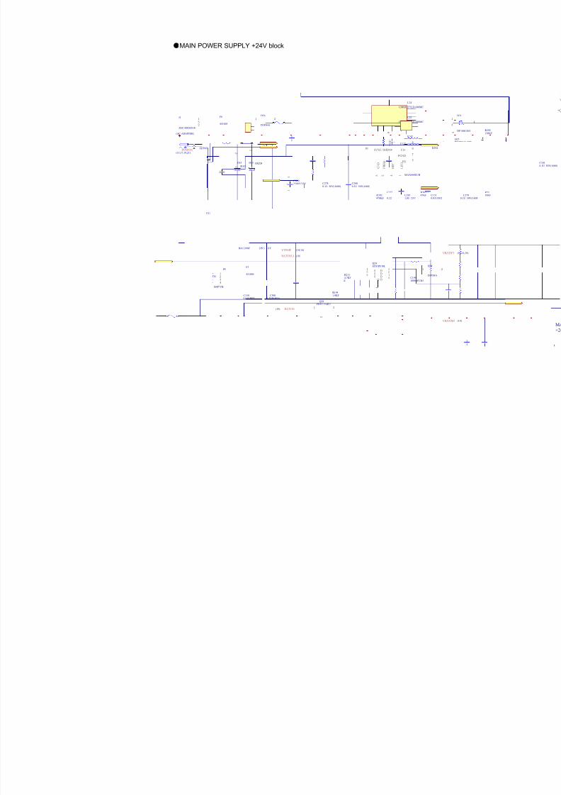
8/13/2019 Manual de Service Fcp-7101 - Fx-7102
http://slidepdf.com/reader/full/manual-de-service-fcp-7101-fx-7102 111/170
MAIN POWER SUPPLY +24V block
SYNC/SHDN*10
V C C
9
EXT 8
F R E Q
2
R E F
4
L D O
1
CS+ 6
PGND 7
FB 5
G N D
3
IC42
MAX668EUB
C277
0.22R392470KF
POWON R394
100F
R383
47KF
+TH--
R2114.7KFC149
0.01UFFZ
R194
1.0KF
C1991000pFCHJ
BATON
VBAT(M)
VTEMPJP33 0FR411390F
C1500.01UFFZ
BATSNS_LVBAT(P)
(AC ADAPTER)
R4120.01F(1W)
C2780.1U 50V(1608)
C2790.1U 50V(1608C1510.01UFFZ
C2800.1U 50V(1608)
C2851.0U 25V
L24
CDRH127/LD-680MC
L25
CDRH127/LD-680MC
1
4
3
Q25PSMN010-55D
C3004.7UF(50V)
41
3
D26
DF10SC4M
1 3
2
Q28PDTC124EU
F3
451005
SUPON
31
2
J1
2DC-0005D100
1
2
D53
SL03
1
2
D55 CRZ24
1234
P8
B4P-VH
1 2D56
D3FS4A
1 2D54
D3FS4A
S1
S2
S3
D 5
D 6
D 7
D 8
G
4
Q24STS7PF30L
(19)
(18)
(15,17,19,21)
(14)
(14,16,18)(14,16)
2
1
+ C 100220UF/35V
F6
451003
DG
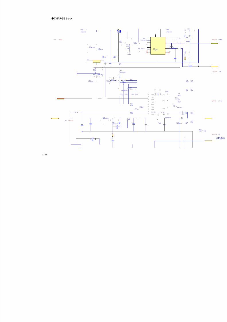
8/13/2019 Manual de Service Fcp-7101 - Fx-7102
http://slidepdf.com/reader/full/manual-de-service-fcp-7101-fx-7102 112/170
5 - 38
CHARGE block
IN3
OUT 1
G N D
2
IC43 NJM78L05UA
C1520.01UFFZ
2
1
+ C31 033uF/10V(C)
R5710KF
CHGENA
C650.1uFFZ
R208 2.0KF
C660.1uFFZ
R5812KF
R5912KF
R38 4 4 7K F
C200 1000pFCHJ
R1951.0KF
C670.1uFFZ
C2011000pFCHJ
R41351KF
JP340F
R2124.7KF
R2134.7KF
R6010KF
R6110KF
R228100F
R396150KF
1
3
2
Q82SC2873
R4171.5KF
JP350F
1
2
D28 D3FS4A C2021000pFCHJ
VCHG
R4202.7KF
R4213.3KF
R423
330KF
R424
330KF
C2861.0U 25V
L26
CDRH127/LD-680MC
R196
1.0KF(1608)
3 1
2D341PS184
3 1
2
D35
1PS184
1
2
D36
1PS184
R422
2.7KF(1608)
1
43
Q392SJ529
2
1
+
C301100UF/35V
C3054.7UF(50V)
I N H *
1 6
L E D 2
1 1
TS 7
BAT 8
MOD14
TCO6
TM14
VCC13
VSS12
DSEL2
DCMD*1
SNS 9
L E D 1
1 0
TM25
DIS 15
VSEL3
IC44
BQ2004ESN
1 3
2
Q42PDTA124EU
1 3
2
Q29PDTC124EU
1
3
D33
BZX84-B16
1
3
D27
BZX84-B5V6
3
2
1
Q412SK2112
1 2D40
D3FS4A
(17)
(13)
2
1
+ C29 4100UF/35V
DG
+5VSTB
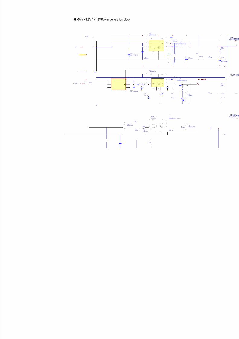
8/13/2019 Manual de Service Fcp-7101 - Fx-7102
http://slidepdf.com/reader/full/manual-de-service-fcp-7101-fx-7102 113/170
+5V / +3.3V / +1.8VPower generation block
C680.1uFFZ
C1530.01UFFZ
1
2
D29
D3FS4A
5VON
C690.1uFFZ
C1540.01UFFZ
1
2
D30
D3FS4A
POWON
1
2
D31
D3FS4A
G N D
3
LX 7
IN8
VCC1
FB 4
COMP5
P G N D
6
REF 2
IC45MAX1952
R6210F
2
1
+ C3 13
33uF/10V(C)
C700.1uFFZ
R414
68KF
C316220pFCHJ
C710.1uFFZ
2
1
+ C 317220uF/6.3V(C)C72
0.1uFFZ
C2810.1U 50V(1608)
C2820.1U 50V(1608)
L32
CDRH2D18/HP-2R2NC
L27
CDRH127/LD-680MC
L33
CDRH127/LD-820MC
VSW 8
*
2
G N
D
6
CB 1
FB
4
VIN7
ON/OFF*
5
*3
IC46LM2674M-3.3
VSW 8
*
2
G N D
6
CB 1
FB 4
VIN7
ON/OFF*5
*3
IC47LM2674M-5.0
3.3VON
+24V
(19)
(13,17,19,21)
2
1
+ C 311220UF/35V
2
1
+ C 312220UF/35V
DG
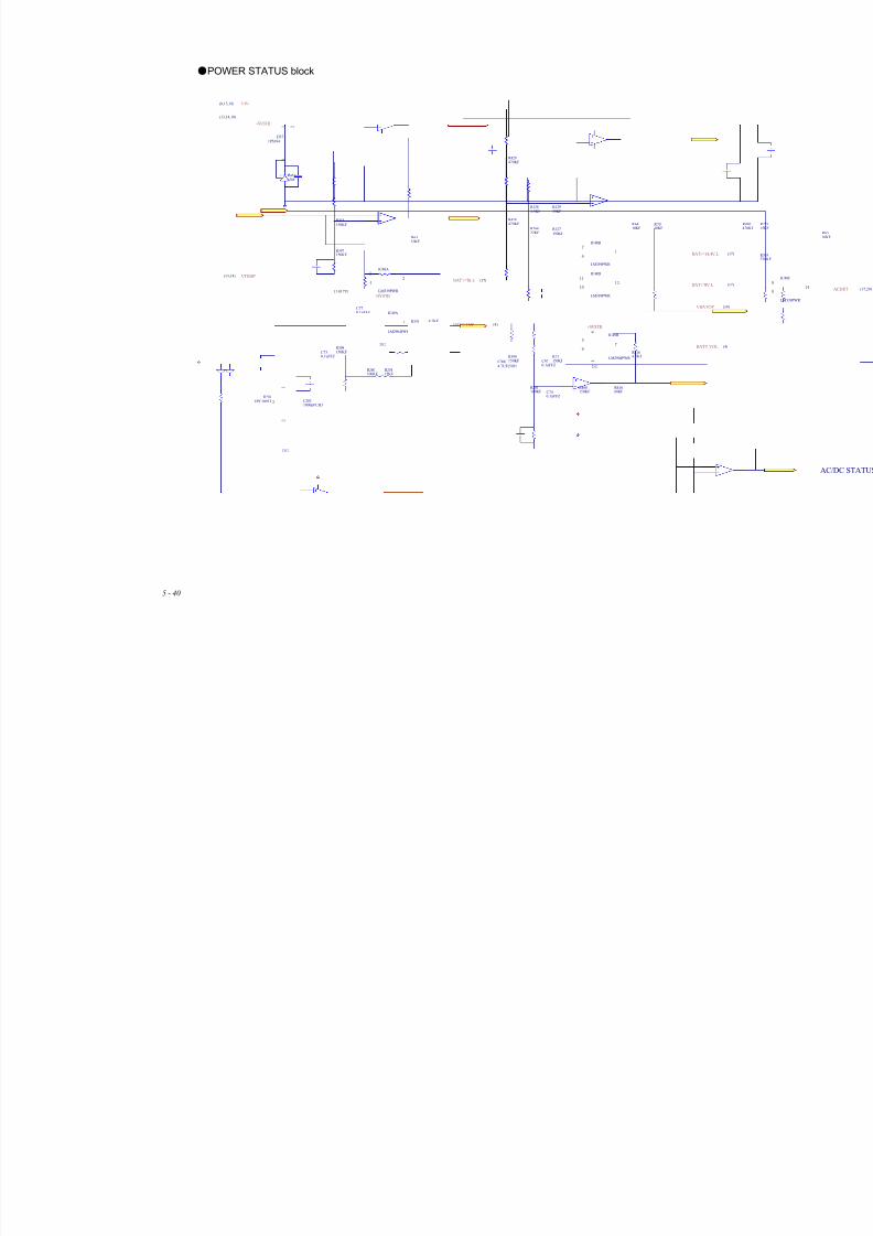
8/13/2019 Manual de Service Fcp-7101 - Fx-7102
http://slidepdf.com/reader/full/manual-de-service-fcp-7101-fx-7102 114/170
5 - 40
POWER STATUS block
R415150KF
R397150KF
25
4
IC48A
LM339PWR
R398150KFC73
0.1uFFZ
R25415KF
R280100KF
R6310KF
[1.017V]
VTEMPBAT>=70_L
17
6
IC48B
LM339PWR
R428470KF
R429470KF
R26822KF
VBAT(P)
R399150KF
R281100KF C74
0.1uFFZ
R400150KF
R41668KF
R2164.7KF
R6410KF
VIN
BAT>=14.4V_L
VBATOP
R4
R4C155
0.01UF
2
3
1
IC50UPC1093T
R433620F
C2031000pFCHJ
3
1 2
D371PS184
C3064.7UF(50V)
BATT_VOL
BATT_TMP
DG
+5VSTB
(17)
(17)
(4)
(4)
(13,14,18)
(19)
(8,13,18)
(13,14)
3
21
8
4
IC49A
LM2904PWR
5
67
8
4
IC49B
LM2904PWR
+5VSTB
+5VSTB
C770.1uFFZ
1311
10
IC48D
LM339PWR
R7010KFR127
150KF
R71150KFC97
0.1uFFZ
R1283.9KF
R12939KF
BAT<=8V_L (17)
DG
DG
R336 4.7KF
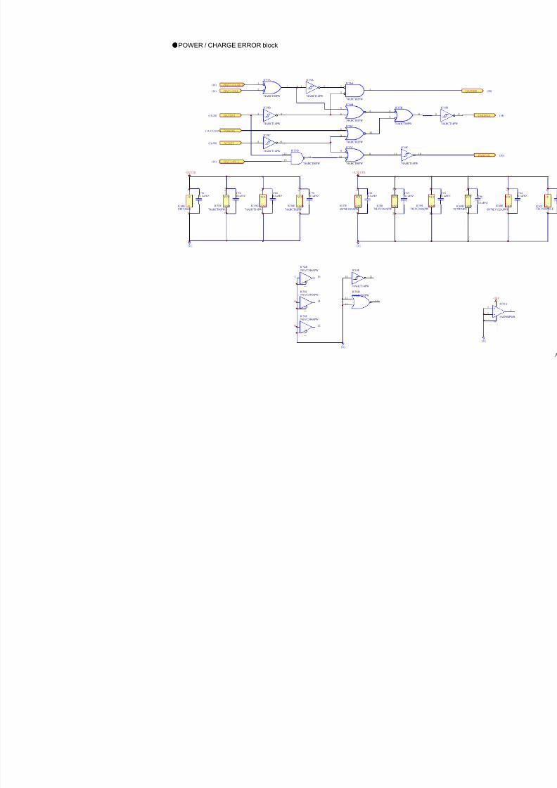
8/13/2019 Manual de Service Fcp-7101 - Fx-7102
http://slidepdf.com/reader/full/manual-de-service-fcp-7101-fx-7102 115/170
POWER / CHARGE ERROR block
1
23
IC53A
74AHCT00PW
2
31
IC56A
74AHCT02PW
5
64
IC56B
74AHCT02PW
8
910
IC56C
74AHCT02PW
4
56
IC53B
74AHCT00PW
9
108
IC53C
74AHCT00PW
BAT>=14.4V_L
BAT>=70_L
BATDET
POWON
ACDET
BATER
3
1 2
+V
-VIC48EUPC339G2
1 4
7
VCC
GNDIC53E
74AHCT00PW
1 4
7
VCC
GNDIC56E
74AHCT02PW
C760.1uFFZ
C780.1uFFZ
C790.1uFFZ
C800.1uFFZ
C820.1uFFZ
2 0
1 0
VCC
GNDIC58I74LVC244APW
2 0
1 0
VCC
GNDIC59I74LVC240APW
C830.1uFFZ
+3.3VSTB
V C C
8
G N D
4
VCC
GNDIC69BTC7W74FU
(16,20)
(16)
(16)
(18,20)
(13,15,19,21)
1 2
IC19A
74AHCT14PW
3 4
IC19B
74AHCT14PW
12
1311
IC53D
74AHCT00PW
5 6
IC19C
74AHCT14PW
9 8
IC19D
74AHCT14PW
11 10
IC19E
74AHCT14PW
1 4
7
VCC
GNDIC19G
74AHCT14PW
13 12
IC19F
74AHCT14PW
4 16
1
IC58B74LVC244APW
6 14
1
IC58C74LVC244APW
8 12
1
IC58D74LVC244APW
BAT<=8V_L(16)
DG
DG
+5VSTB
DG
11
1213
IC56D74AHCT02PW
1 4
7
VCC
GNDIC57E
SN74LV02APW
C810.1uFFZ
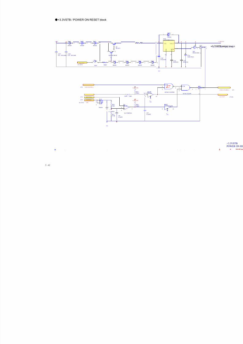
8/13/2019 Manual de Service Fcp-7101 - Fx-7102
http://slidepdf.com/reader/full/manual-de-service-fcp-7101-fx-7102 116/170
5 - 42
+3.3VSTB / POWER ON RESET block
1
32
Q92SC2873
1
23
Q44 2PC4081R
14
D43A
BAS28
23
D43B
BAS28
14
D44A
BAS28
23D44B
BAS28
14D45A
BAS28
23D45B
BAS28
1 4D46A
BAS28
23D46B
BAS28
R283
100KF
R229 100F
V S S
2
C D
3
VOUT 1
VOR 4
VIN5
IC62S-873325BUP-ALA
C1560.01UFFZ
C1570.01UFFZ
VBAT(P)
5
64
IC57B
SN74LV02APW
R38647KF
R2174.7 KF C86
0.1uFFZ
4 16
1
IC59B74LVC240APW
6 14
1
IC59C74LVC240APW
C870.1uFFZ
R284100KF
R269 22KF
R434820KF
VBATGOOD_L
BATSNS_L
CMPREF
VIN
+3.3VSTB
+3.3VSTB
75
6
IC61B
TLC393IPWLE
31
2
D38
1PS184
C3074.7UF(50V)
C3084.7UF(50V)
1 3
2
Q43PDTA124EU
1 3
2
Q34PDTC124EU
1 3
2
Q35PDTC124EU
4
56
IC60B
SN74LV132APWR
DG
DG
DG
DG
+24V
1 2
D47
SL03
(13)
(19)
(13,14,16)
(19)
(8,13,16)
C2970.1U 50V(1608)
C2980.1U 50V(1608)
2
1
+ C31433uF/10V(C)
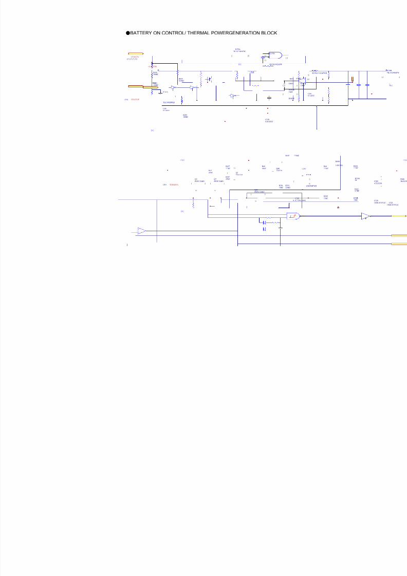
8/13/2019 Manual de Service Fcp-7101 - Fx-7102
http://slidepdf.com/reader/full/manual-de-service-fcp-7101-fx-7102 117/170
BATTERY ON CONTROL/ THERMAL POWERGENERATION BLOCK
+3.3VSTB
11
1213
IC57D
SN74LV02APW
R436300KF
R401150KF
R435820KF
VBATOP
R402150KF C88
0.1uFFZ
POWON
R285100KF
R431 470KF
R1971.0KF1 4
D48A
BAS28
C890.1uFFZ
2 3
D48B
BAS28
C1580.01UFFZ
13
2
IC61A
TLC393IPWLE
9
108
IC60CSN74LV132APWR
DG
(13,15,17,21)
(16)
2 18
1
IC59A74LVC240APW
DG
R437
2.2KF
R38747KF
R38810KF
R38915KF
R407 220KF
R68
10KF
THRMON
R440
1.0F(1W)
C2830.1U 50V(1608)
1
43
Q402SJ529
+24V
(20) 1 3
2
Q3PDTC124EU
1 3
2
Q7PDTC124EU
1 3
2
Q26PDTC124EU
1
2
3
Q22SA1163
R66
2.2KFR6747KF
5
67
8
4
IC51B
LM2904PWR
+24V
R391220KF
DG
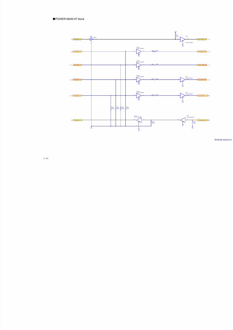
8/13/2019 Manual de Service Fcp-7101 - Fx-7102
http://slidepdf.com/reader/full/manual-de-service-fcp-7101-fx-7102 118/170
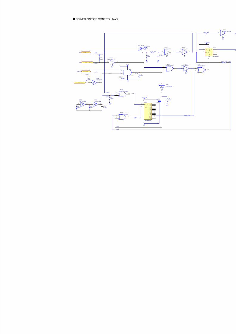
8/13/2019 Manual de Service Fcp-7101 - Fx-7102
http://slidepdf.com/reader/full/manual-de-service-fcp-7101-fx-7102 119/170
POWER ON/OFF CONTROL block
CLK10
RST11
Q1 9
Q2 7
Q3 6
Q4 5
Q5 3
Q6 2
Q7 4
Q8 13
Q9 12
Q10 14
Q11 15
Q12 1
1 6
8
IC64
74HC4040PW
R231 100F
C910.1uFFZ
DG
3
21
D24 1PS302+3.3VSTB
DG
R7310KF
DGPOW_ON_RES_L
+3.3VSTB
R7610KF
(STB)
(STB)
(STB)
(STB)
(STB)(STB)
(STB)
(3.3V)(3.3V)
(3.3V)
(3.3V)
+3.3V
DG
C92
0.1uFFZ
+3.3VSTB
DG
C980.1uFFZ
COUNT"200"
POWER_OFF_L
RESET_L
POW
3 5
IC18B
74HC3G14DP
98
10
1 4
7
IC6C
74HC08PW
(8)
(18)
(3,4,5,6,8)
R56100KF
2
31
IC57A
SN74LV02APW
8
9
IC57C
SN74L
1
23
IC60A
SN74LV132APWR
R75100KF
DG3 5
IC2B
74HC3G14DP
6 2
IC2C
74HC3G14DP
R92100KF
R12651KF
C940.1uFFZ
15 5
1 9
IC59G74LVC240APW
8 12
1
IC59D74LVC240APW
DG
DG
11 9
1 9
IC59E74LVC240APW
13 7
1 9
IC59F74LVC240APW
DG
DG
R43910KF
12
1311
IC60D
SN74LV132APWR
+3.3V
6
2
IC18C
74HC3G14DP
R473100KF
DG
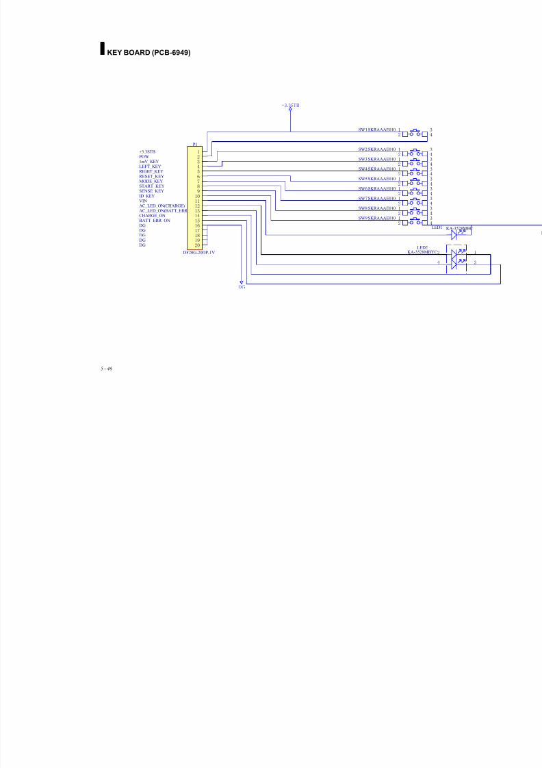
8/13/2019 Manual de Service Fcp-7101 - Fx-7102
http://slidepdf.com/reader/full/manual-de-service-fcp-7101-fx-7102 120/170
5 - 46
KEY BOARD (PCB-6949)
12
34
SW1 SKRAAAE010
POW1mV_KEYLEFT_KEYRIGHT_KEYRESET_KEYMODE_KEYSTART_KEY
VIN
CHARGE_ONBATT_ERR_ON
AC_LED_ON(CHARGE)AC_LED_ON(BATT_ERR)
+3.3STB
DG
+3.3STB
DG
12
34
SW2 SKRAAAE010
12
34
SW3 SKRAAAE010
12
34
SW4 SKRAAAE010
12
34
SW5 SKRAAAE010
12 34SW6 SKRAAAE010
12
34
SW7 SKRAAAE010
SENSE_KEY
12
34
SW8 SKRAAAE010
LED1 KA-3528
2
4
LED2KA-3528MBYC
ID_KEY
12
34
SW9 SKRAAAE010
DGDGDGDG
123456789
1011121314151617181920
P1
DF20G-20DP-1V

8/13/2019 Manual de Service Fcp-7101 - Fx-7102
http://slidepdf.com/reader/full/manual-de-service-fcp-7101-fx-7102 121/170
SENSOR BOARD (PCB-6948)
SENSOR-COM
MARK-E
LED_DRIVE
DETECT-E12345
DF13B-5P-1.25V(21)
TO MAIN BOARD MARK SENSPCB-694
12345
P2
DF13-5S-1.25C
SENSOR CABLE
12345
P1
DF4-5P-2C
NC
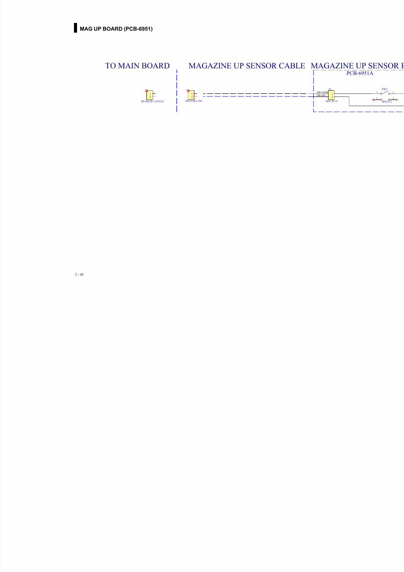
8/13/2019 Manual de Service Fcp-7101 - Fx-7102
http://slidepdf.com/reader/full/manual-de-service-fcp-7101-fx-7102 122/170
5 - 48
MAG UP BOARD (PCB-6951)
12
P1
DF4-2P-2C
SW-ONSW-COM
12
DF13B-2P-1.25V(21)
TO MAIN BOARD MAGAZIN
12
DF13-2S-1.25C
MAGAZINE UP SENSOR CABLE
8/13/2019 Manual de Service Fcp-7101 - Fx-7102
http://slidepdf.com/reader/full/manual-de-service-fcp-7101-fx-7102 123/170

8/13/2019 Manual de Service Fcp-7101 - Fx-7102
http://slidepdf.com/reader/full/manual-de-service-fcp-7101-fx-7102 124/170
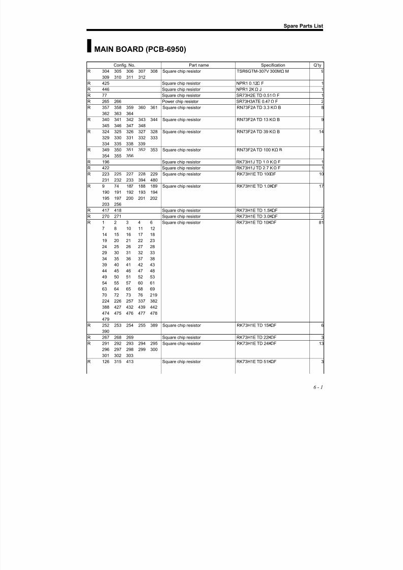
8/13/2019 Manual de Service Fcp-7101 - Fx-7102
http://slidepdf.com/reader/full/manual-de-service-fcp-7101-fx-7102 125/170
Spare Parts List
6 - 1
MAIN BOARD (PCB-6950)
Config. No. Part name Specification Q’ty
R 304 305 306 307 308 Square chip resistor TSR6GTM-307V 300M Ω M 9
309 310 311 312
R 425 Square chip resistor NPR1 0.12Ω F 1
R 446 Square chip resistor NPR1 2K Ω J 1
R 77 Square chip resistor SR73H2E TD 0.51 Ω F 1
R 265 266 Power chip resistor SR73H3ATE 0.47 Ω F 2
R 357 358 359 360 361 Square chip resistor RN73F2A TD 3.3 K Ω B 8
362 363 364
R 340 341 342 343 344 Square chip resistor RN73F2A TD 13 K Ω B 9
345 346 347 348
R 324 325 326 327 328 Square chip resistor RN73F2A TD 39 K Ω B 14
329 330 331 332 333
334 335 338 339
R 349 350 351 352 353 Square chip resistor RN73F2A TD 100 K Ω B 8
354 355 356
R 196 Square chip resistor RK73H1J TD 1.0 K Ω F 1
R 422 Square chip resistor RK73H1J TD 2.7 K Ω F 1
R 223 225 227 228 229 Square chip resistor RK73H1E TD 100ΩF 10
231 232 233 394 480
R 9 74 187 188 189 Square chip resistor RK73H1E TD 1.0KΩF 17
190 191 192 193 194
195 197 200 201 202
203 256
R 417 418 Square chip resistor RK73H1E TD 1.5KΩF 2R 270 271 Square chip resistor RK73H1E TD 3.0KΩF 2
R 1 2 3 4 6 Square chip resistor RK73H1E TD 10KΩF 81
7 8 10 11 12
14 15 16 17 18
19 20 21 22 23
24 25 26 27 28
29 30 31 32 33
34 35 36 37 38
39 40 41 42 43
44 45 46 47 48
49 50 51 52 53
54 55 57 60 61
63 64 65 68 69
70 72 73 76 219
224 226 257 337 382
388 427 432 439 442
474 475 476 477 478
479
R 252 253 254 255 389 Square chip resistor RK73H1E TD 15KΩF 6
390
R 267 268 269 Square chip resistor RK73H1E TD 22KΩF 3
R 291 292 293 294 295 Square chip resistor RK73H1E TD 24KΩF 13
296 297 298 299 300
301 302 303
R 126 315 413 Square chip resistor RK73H1E TD 51KΩF 3
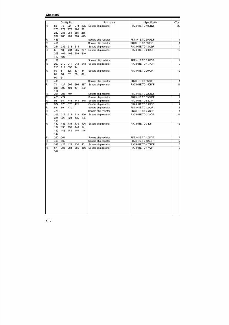
8/13/2019 Manual de Service Fcp-7101 - Fx-7102
http://slidepdf.com/reader/full/manual-de-service-fcp-7101-fx-7102 126/170
Chapter6
6 - 2
Config. No. Part name Specification Q’ty
R 56 75 92 274 275 Square chip resistor RK73H1E TD 100KΩF 20
276 277 278 280 281
282 283 284 285 286
287 288 289 290 473
R 436 Square chip resistor RK73H1E TD 300KΩF 1R 411 Square chip resistor RK73H1E TD 390ΩF 1
R 234 235 313 314 Square chip resistor RK73H1E TD 1.0MΩF 4
R 5 13 204 205 207 Square chip resistor RK73H1E TD 2.0KΩF 12
208 404 408 409 410
419 426
R 128 Square chip resistor RK73H1E TD 3.9KΩF 1
R 209 210 211 212 213 Square chip resistor RK73H1E TD 4.7KΩF 9
216 217 336 441
R 80 81 82 83 84 Square chip resistor RK73H1E TD 20KΩF 12
85 86 87 88 89
90 91
R 403 Square chip resistor RK73H1E TD 33KΩF 1
R 71 127 395 396 397 Square chip resistor RK73H1E TD 150KΩF 11
398415
399 400 401 402
R 391 393 407 Square chip resistor RK73H1E TD 220KΩF 3
R 423 424 Square chip resistor RK73H1E TD 330KΩF 2
R 93 94 443 444 445 Square chip resistor RK73H1E TD 680ΩF 5
R 374 375 376 471 Square chip resistor RK73H1E TD 1.2KΩF 4
R 58 59 470 Square chip resistor RK73H1E TD 12KΩF 3
R 420 Square chip resistor RK73H1E TD 2.7KΩF 1
R 316 317 318 319 320 Square chip resistor RK73H1E TD 3.3KΩF 11
321
421
322 323 405 406
R 132 133 134 135 136 Square chip resistor RK73H1E TD 33ΩF 16
137 138 139 140 141
142 143 144 145 146
147
R 260 261 Square chip resistor RK73H1E TD 4.3KΩF 2
R 468 469 Square chip resistor RK73H1E TD 422ΩF 2
R 392 428 429 430 431 Square chip resistor RK73H1E TD 470KΩF 5
R 67 383 384 385 386 Square chip resistor RK73H1E TD 47KΩF 6
387
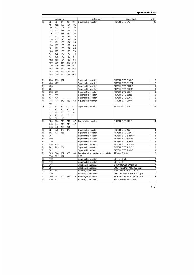
8/13/2019 Manual de Service Fcp-7101 - Fx-7102
http://slidepdf.com/reader/full/manual-de-service-fcp-7101-fx-7102 127/170
Spare Parts List
6 - 3
Config. No. Part name Specification Q’ty
R 95 96 97 98 99 Square chip resistor RK73H1E TD 51ΩF 96
101 102 103 104 105
106 107 108 109 110
111 112 113 114 115
116 117 118 119 120121 122 123 124 125
130 131 148 149 150
151 152 153 154 155
156 157 158 159 160
161 162 163 164 165
166 167 168 169 170
171 172 173 175 176
177 178 179 180 181
182 183 184 185 186
199 206 214 215 218
220 230 236 237 447
448 449 450 451 452
453 454 455 456 457
458 459 460 461 462
472
R 238 239 377 Square chip resistor RK73H1E TD 510ΩF 3
R 466 467 Square chip resistor RK73H1E TD 61.9ΩF 2
R 433 Square chip resistor RK73H1E TD 620ΩF 1
R 78 Square chip resistor RK73H1E TD 62KΩF 1
R 272 273 Square chip resistor RK73H1E TD 68ΩF 2
R 414 416 Square chip resistor RK73H1E TD 68KΩF 2
R 434 435 Square chip resistor RK73H1E TD 820KΩF 2
R 221 222 279 463 464 Square chip resistor RK73H1E TD 300ΩF 6
465
JP 1 2 3 4 5 Square chip resistor RK73Z1E TD 0ΩF 23
6 7 8 9 10
11 12 16 17 18
19 25 26 27 33
34 35 198
R 100 174 240 241 242 Square chip resistor RK73H1E TD 22ΩF 14
243 244 245 246 247
248 249 250 251
R 62 373 378 379 Square chip resistor RK73H1E TD 10ΩF 4
R 66 437 438 Square chip resistor RK73H1E TD 2.2KΩF 3
R 79 Square chip resistor RK73H1E TD 3.24KΩF 1R 380 Square chip resistor RK73H1E TD 330ΩF 1
R 129 Square chip resistor RK73H1E TD 39KΩF 1
R 258 259 Square chip resistor RK73H1E TD 7.15KΩF 2
R 262 263 264 Square chip resistor RK73H1E TD 7.5KΩF 3
R 381 Square chip resistor RK73H1E TD 910ΩF 1
R 365 366 367 368 369 TRN60LG 3.5M 8
370 371 372
Tantalum alloy resistance on cylinderside
R 412 Square chip resistor SL1TE 10m F 1
R 440 Square chip resistor SL1TE 1.0F 1
C 317 Electrolytic capacitor 6.3CV220AX 6.3V 220 µF 1
C 204 Electrolytic capacitor UUD1V680MCR1GS 35V 68µF 1
C 294 301 Electrolytic capacitor MVE35V100MF80 35V 100 2
C 179 Electrolytic capacitor UUD1H220MCR1GS 50V 22µF 1
C 100 101 102 311 312 Electrolytic capacitor MVE35VC220MJ10 220µF/35V 5
C 320 321 Electrolytic capacitor 35CV1500AX 35V 1500 2
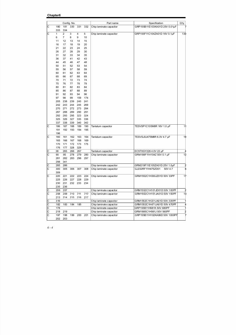
8/13/2019 Manual de Service Fcp-7101 - Fx-7102
http://slidepdf.com/reader/full/manual-de-service-fcp-7101-fx-7102 128/170
Chapter6
6 - 4
Config. No. Part name Specification Q’ty
C 180 181 330 331 332 Chip laminate capacitor GRP155B11E103KA01D 25V 0.01µF 7
333 334
C 1 2 3 4 5 Chip laminate capacitor GRP155F11C104ZA01D 16V 0.1µF 130
6 7 8 9 10
11 12 13 14 1516 17 18 19 20
21 22 23 24 25
26 27 28 29 30
31 32 33 34 35
36 37 41 42 43
44 45 46 47 48
50 51 52 53 54
55 56 57 58 59
60 61 62 63 64
65 66 67 68 69
70 71 72 73 74
75 76 77 78 79
80 81 82 83 84
85 86 87 88 89
91 92 93 94 96
97 98 99 159 174
205 238 239 240 241
242 243 244 245 269
270 271 272 273 284
287 288 289 290 291
292 293 295 323 324
325 326 327 335 336
337 338 339 340 342
C 186 187 188 189 190 Tantalum capacitor TESVSP1C105M8R 16V 1.0 µF 11
191 192 193 194 195
196
C 160 161 162 163 164 Tantalum capacitor TESVSJ0J475M8R 6.3V 4.7 µF 19
165 166 167 168 169
170 171 172 173 175
176 177 328 329
C 38 265 266 267 Tantalum capacitor ECST0GY226 4.0V 22 µF 4
C 90 95 278 279 280 Chip laminate capacitor GRM188F11H104Z 50V 0.1 µF 12
281 282 283 296 297
298 341
C 285 286 Chip laminate capacitor GRM219F11E105ZA01D 25V 1.0µF 2C 300 305 306 307 308 Chip laminate capacitor GJ232RF11H475ZD01 50V 4.7 6
309
C 220 221 222 223 224 Chip laminate capacitor GRM1552C1H330JZ01D 50V 33PF 17
225 226 227 228 229
230 231 232 233 234
235 236
C 206 207 Chip laminate capacitor GRM1552C1H101JD01D 50V 100PF 2
C 208 209 210 211 212 Chip laminate capacitor GRM1552C1H151JA01D 50V 150PF 10
213 214 215 216 217
C 316 Chip laminate capacitor GRM1552C1H221JA01D 50V 220PF 1
C 182 183 184 185 Chip laminate capacitor GRM1552C1H471JA01D 50V 470PF 4
C 178 Chip laminate capacitor GRP155B11H681K 50V 680PF 1
C 218 219 Chip laminate capacitor GRM1885C1H561J 50V 560PF 2
C 197 198 199 200 201 Chip laminate capacitor GRP155B11H102KA86D 50V 1000PF 7
202 203

8/13/2019 Manual de Service Fcp-7101 - Fx-7102
http://slidepdf.com/reader/full/manual-de-service-fcp-7101-fx-7102 129/170
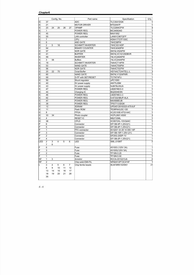
8/13/2019 Manual de Service Fcp-7101 - Fx-7102
http://slidepdf.com/reader/full/manual-de-service-fcp-7101-fx-7102 130/170
Chapter6
6 - 6
Config. No. Part name Specification Q’ty
IC 37 ADC TLC3541DGK 1
IC 21 MOTOR DRIVER MTD2007F 1
IC 23 24 25 26 27 OPAMP TLC2264CPW 5
IC 1 POWER REG. MC34063AD 1
IC 45 POWER REG. MAX1952 1IC 55 LAN controller LAN91C96TQFP 1
IC 7 CPU HD6417727F100C 1
IC 6 AND GATE 74HC08PW 1
IC 2 5 18 SCHIMITT INVERTER 74HC3G14DP 3
IC 64 BINARY COUNTER 74HC4040PW 1
IC 57 NOR GATE SN74LV02APW 1
IC 41 BUFFER SN74LVC1G125DBVR 1
IC 59 INVERTER 74LVC240APW 1
IC 3 58 Buffers 74LVC244APW 2
IC 19 SCHIMITT INVERTER 74AHCT14PW 1
IC 53 NAND GATE 74AHCT00PW 1
IC 56 NOR GATE 74AHCT02PW 1
IC 20 22 70 Octal Buffer HD74ACT244TELL-L 3
IC 60 NAND GATE SN74LV132APWR 1
IC 69 D-FF with SET/RESET TC7W74FU 1
IC 50 Shunt regulator uPC1093 1
IC 40 5V power supply AN77L05M 1
IC 43 5V power supply NJM78L05UA 1
IC 47 POWER REG. LM2674M-5.0 1
IC 44 Charging IC BQ2004ESN 1
IC 46 POWER REG. LM2674M-3.3 1
IC 62 POWER REG. S-873325BUP-ALA 1
IC 42 POWER REG. MAX668EUB 1
IC 39 POWER REG. TPS77133DGK 1
IC 12 SDRAM UPD45128163G5-A75-9JF 1
IC 11 Flash ROM TE28F640J3C-120 1
IC 8 FPGA XC2S100E-6TQ144C 1
IC 33 34 Photo coupler HCPL2601 #300 2
IC 4 RESET IC M62733ML 1
IC 38 CPLD XC9572XL-10VQ44C 1
P 6 Connector DF13B-5P-1.25V(21) 1
P 5 Connector DF13B-4P-1.25V(21) 1
P 1 FFC connector 00 6207 33 29 14 000 14P 1
P 3 Connector DF13B-15P-1.25V (21) 1
P 2 Connector DF20G-20DP-1V 1P 4 Connector DF13B-2P-1.25V(21) 1
LED 2 3 4 5 6 LED SML-210MT 7
7 8
F 6 Fuse 451003 (125V 3A) 1
F 3 Fuse 451005(125V 5A) 1
F 2 Fuse TF16N 0.25 1
F 1 Fuse TF16N 0.50 1
NF 1 3 Arrestor RCCA-201Q31UA 2
NF 2 Chip solid EMI-FIL NFM2012P13C474F 1
L 3 4 5 6 7 Chip ferrite beads BLM18RK102SN1 21
8 9 10 11 12
13 14 15 16 17
18 19 20 21 28
35
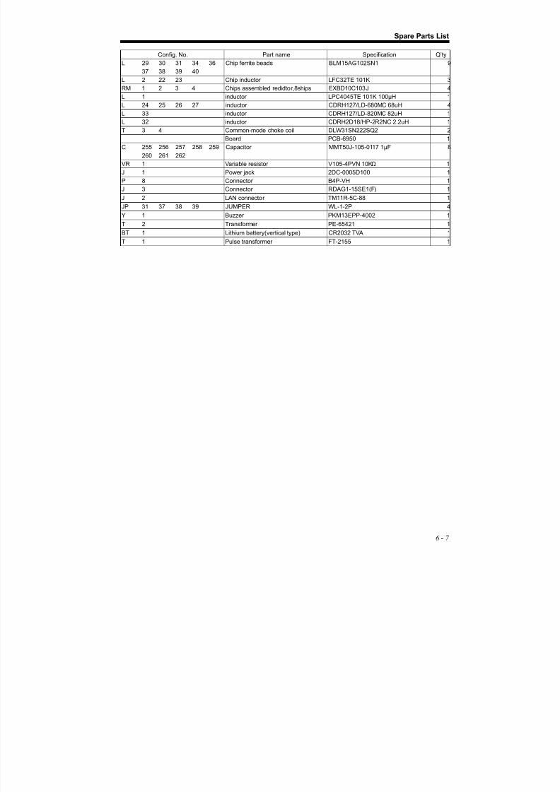
8/13/2019 Manual de Service Fcp-7101 - Fx-7102
http://slidepdf.com/reader/full/manual-de-service-fcp-7101-fx-7102 131/170
Spare Parts List
6 - 7
Config. No. Part name Specification Q’ty
L 29 30 31 34 36 Chip ferrite beads BLM15AG102SN1 9
37 38 39 40
L 2 22 23 Chip inductor LFC32TE 101K 3
RM 1 2 3 4 Chips assembled redidtor,8ships EXBD10C103J 4
L 1 inductor LPC4045TE 101K 100µH 1L 24 25 26 27 inductor CDRH127/LD-680MC 68uH 4
L 33 inductor CDRH127/LD-820MC 82uH 1
L 32 inductor CDRH2D18/HP-2R2NC 2.2uH 1
T 3 4 Common-mode choke coil DLW31SN222SQ2 2
Board PCB-6950 1
C 255 256 257 258 259 Capacitor MMT50J-105-0117 1µF 8
260 261 262
VR 1 Variable resistor V105-4PVN 10KΩ 1
J 1 Power jack 2DC-0005D100 1
P 8 Connector B4P-VH 1
J 3 Connector RDAG1-15SE1(F) 1
J 2 LAN connector TM11R-5C-88 1
JP 31 37 38 39 JUMPER WL-1-2P 4
Y 1 Buzzer PKM13EPP-4002 1
T 2 Transformer PE-65421 1
BT 1 Lithium battery(vertical type) CR2032 TVA 1
T 1 Pulse transformer FT-2155 1

8/13/2019 Manual de Service Fcp-7101 - Fx-7102
http://slidepdf.com/reader/full/manual-de-service-fcp-7101-fx-7102 132/170
Chapter6
6 - 8
KEY BOARD (PCB-6949)
Config. No. Part name Specification Q’ty
LED 1 LED(blue) KA-3528MBC 1
LED 2 LED(blue, yellow) KA-3528MBYC 1
P 1 connector DF20G-20DP-1V 1
SW 1 2 3 4 5 Tact switch SKRAAAE010 9
6 7 8 9
Board PCB-6949 1

8/13/2019 Manual de Service Fcp-7101 - Fx-7102
http://slidepdf.com/reader/full/manual-de-service-fcp-7101-fx-7102 133/170
Spare Parts List
6 - 9
SENSOR BOARD (PCB-6948)
Config. No. Part name Specification Q’ty
LED 1 2 Photo sensor EE-SY125 2
Board PCB-6948 1
P 1 Connector DF4-5P-2C 1

8/13/2019 Manual de Service Fcp-7101 - Fx-7102
http://slidepdf.com/reader/full/manual-de-service-fcp-7101-fx-7102 134/170
Chapter6
6 - 10
MAG UP BOARD (PCB-6951)
Config. No. Part name Specification Q’ty
SW 1 Detection switch SPVC2-1 1
Board PCB-6951 1
P 1 connector DF4-2P-2C 1
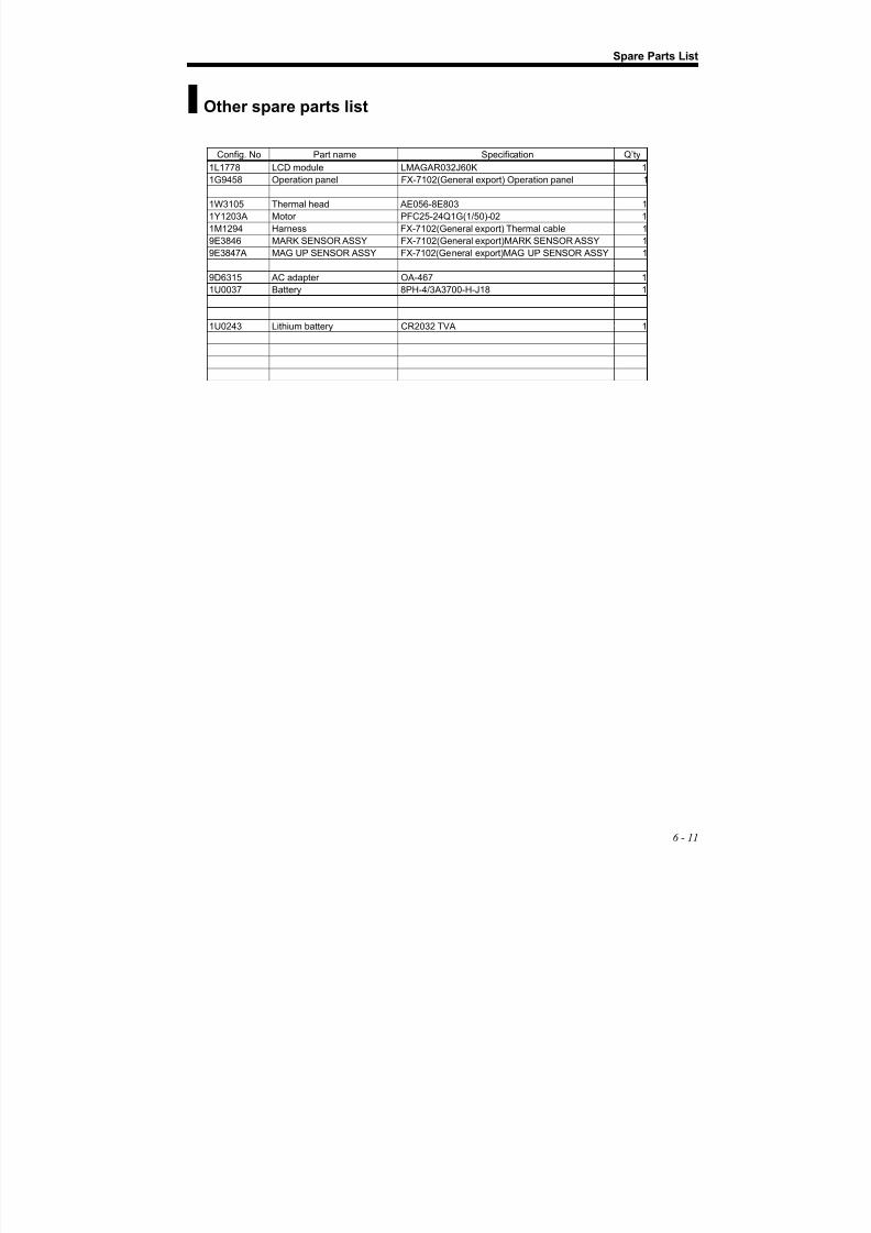
8/13/2019 Manual de Service Fcp-7101 - Fx-7102
http://slidepdf.com/reader/full/manual-de-service-fcp-7101-fx-7102 135/170
Spare Parts List
6 - 11
Other spare parts list
Config. No Part name Specification Q’ty
1L1778 LCD module LMAGAR032J60K 1
1G9458 Operation panel FX-7102(General export) Operation panel 1
1W3105 Thermal head AE056-8E803 1
1Y1203A Motor PFC25-24Q1G(1/50)-02 1
1M1294 Harness FX-7102(General export) Thermal cable 1
9E3846 MARK SENSOR ASSY FX-7102(General export)MARK SENSOR ASSY 1
9E3847A MAG UP SENSOR ASSY FX-7102(General export)MAG UP SENSOR ASSY 1
9D6315 AC adapter OA-467 1
1U0037 Battery 8PH-4/3A3700-H-J18 1
1U0243 Lithium battery CR2032 TVA 1

8/13/2019 Manual de Service Fcp-7101 - Fx-7102
http://slidepdf.com/reader/full/manual-de-service-fcp-7101-fx-7102 136/170
Chapter6
6 - 12
8/13/2019 Manual de Service Fcp-7101 - Fx-7102
http://slidepdf.com/reader/full/manual-de-service-fcp-7101-fx-7102 137/170
Chapter 7
Board Component DiagramMAIN BOARD (PCB-6950component side) .......................................7-1MAIN BOARD (PCB-6950soldering side)...........................................7-2KEY BOARD (PCB-6949component side) ......................................... 7-3KEY BOARD (PCB-6949soldering side) ............................................7-4SENSOR BOARD (PCB-6948component side) .................................7-5MAG UP BOARD (PCB-6951component side) ..................................7-6

8/13/2019 Manual de Service Fcp-7101 - Fx-7102
http://slidepdf.com/reader/full/manual-de-service-fcp-7101-fx-7102 138/170

8/13/2019 Manual de Service Fcp-7101 - Fx-7102
http://slidepdf.com/reader/full/manual-de-service-fcp-7101-fx-7102 139/170
MAIN BOARD (PCB-6950 component side)
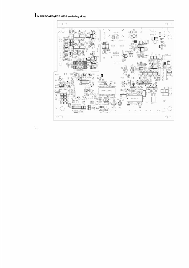
8/13/2019 Manual de Service Fcp-7101 - Fx-7102
http://slidepdf.com/reader/full/manual-de-service-fcp-7101-fx-7102 140/170
7 - 2
MAIN BOARD (PCB-6950 soldering side)
8/13/2019 Manual de Service Fcp-7101 - Fx-7102
http://slidepdf.com/reader/full/manual-de-service-fcp-7101-fx-7102 141/170
KEY BOARD (PCB-6949 component side)
8/13/2019 Manual de Service Fcp-7101 - Fx-7102
http://slidepdf.com/reader/full/manual-de-service-fcp-7101-fx-7102 142/170
7 - 4
KEY BOARD (PCB-6949 soldering side)
8/13/2019 Manual de Service Fcp-7101 - Fx-7102
http://slidepdf.com/reader/full/manual-de-service-fcp-7101-fx-7102 143/170
SENSOR BOARD (PCB-6948 component side)
8/13/2019 Manual de Service Fcp-7101 - Fx-7102
http://slidepdf.com/reader/full/manual-de-service-fcp-7101-fx-7102 144/170
7 - 6
MAG UP BOARD (PCB-6951 component side)

8/13/2019 Manual de Service Fcp-7101 - Fx-7102
http://slidepdf.com/reader/full/manual-de-service-fcp-7101-fx-7102 145/170

8/13/2019 Manual de Service Fcp-7101 - Fx-7102
http://slidepdf.com/reader/full/manual-de-service-fcp-7101-fx-7102 146/170
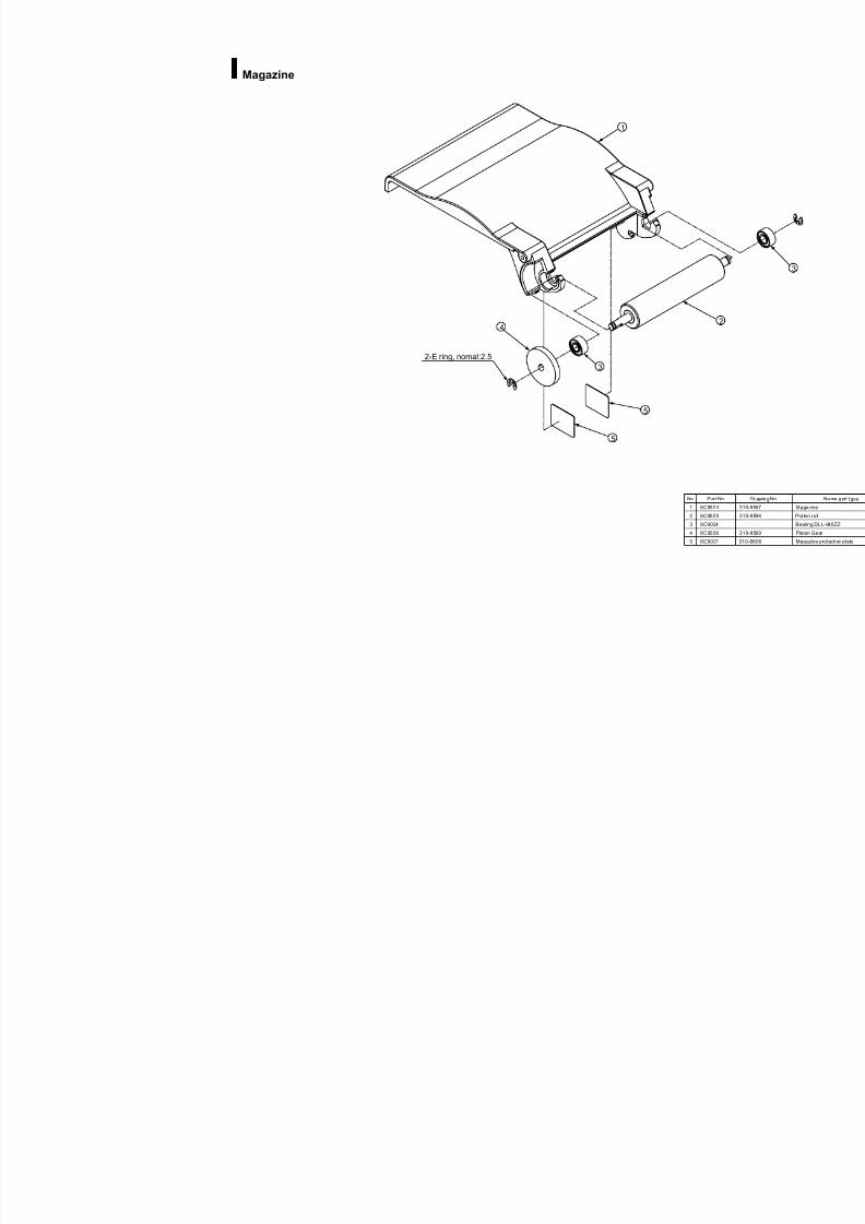
8/13/2019 Manual de Service Fcp-7101 - Fx-7102
http://slidepdf.com/reader/full/manual-de-service-fcp-7101-fx-7102 147/170
Magazine
2-E ring, nomal:2.5
5
5
3
4
1
2
No. P ar t No .
1 6C9023
2 6C9025
3 6C9024
4 6C9026
5 6C9027
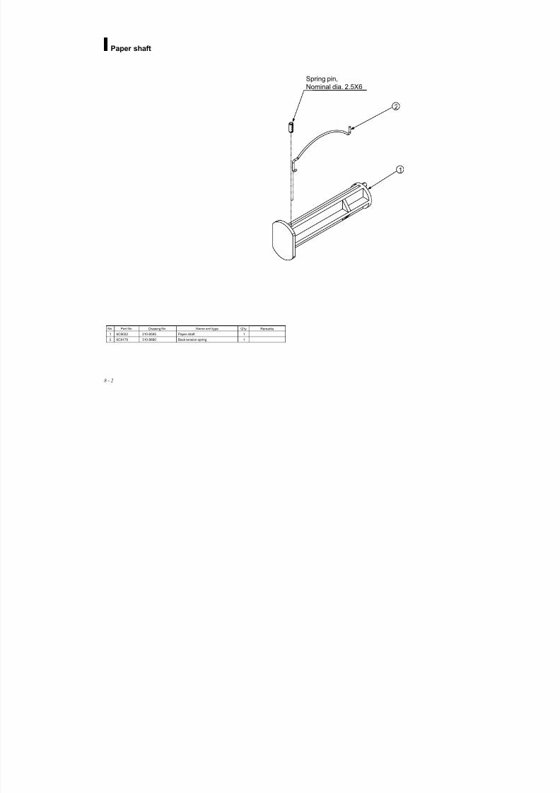
8/13/2019 Manual de Service Fcp-7101 - Fx-7102
http://slidepdf.com/reader/full/manual-de-service-fcp-7101-fx-7102 148/170
8 - 2
Paper shaft
2
1
Spring pin,
Nominal dia. 2.5X6
No. Part No. Drawing No. Name and type Q’ty Remarks
1 6C9022 310-8595 Paper shaft 1
2 6C9179 310-8880 Back tension spring 1
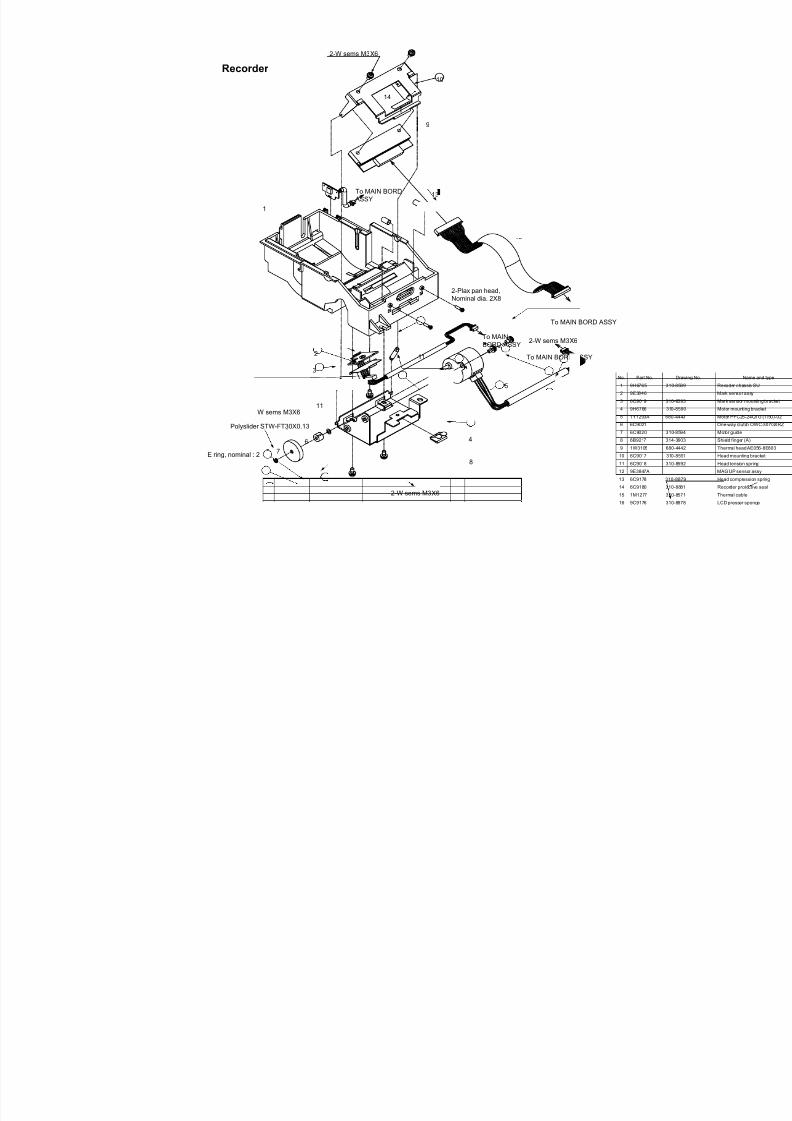
8/13/2019 Manual de Service Fcp-7101 - Fx-7102
http://slidepdf.com/reader/full/manual-de-service-fcp-7101-fx-7102 149/170
Recorder
No. Part No.
1 9H6765 310-
2 9E3846
3 6C9019 310-
4 9H6766 310-
5 1Y1203A 680-
6 6C9021
7 6C9020 310-
8 6B9217 314-
9 1W3105 680-
10 6C9017 310-
11 6C9018 310-
12 9E3847A
13 6C9178 310-
14 6C9180 310-
15 1M1277 310-
16 9C9176 310-
10
2-W sems M3X6
14
9
13
12
1
To MAIN BORD
ASSY
15
To MAIN BORD ASSY
To MAIN BORD ASSY
2-W sems M3X6To MAIN
BORD ASSY
5
11
4
8
2-W sems M3X6
E ring, nominal : 2
6
7
11W sems M3X6
16
3
2
2-Plax pan head,
Nominal dia. 2X8
Polyslider STW-FT30X0.13

8/13/2019 Manual de Service Fcp-7101 - Fx-7102
http://slidepdf.com/reader/full/manual-de-service-fcp-7101-fx-7102 150/170
8 - 4
Upper case (FX-7102)
3
4-W sems M3X6
No. Part No. Drawing No. Name and type Q’ty Remarks
1 5G2191 310-8574 Upper case U 1
2 9F5379A Key board 1
3 6C9147 310-8876 Lock spring 1
4 5G2192 310-8576 FX-7102 Operation panel sheet (English) 1
5 1M1294 310-8564 KEY cable 1

8/13/2019 Manual de Service Fcp-7101 - Fx-7102
http://slidepdf.com/reader/full/manual-de-service-fcp-7101-fx-7102 151/170
Upper case (FCP-7101)
5
4
1
2
3
4-W sems M3X6
No. Part No.
1 5G2191 310-
2 9F5379A
3 6C9147 310-
4 5G2197 310-
5 1M1294 310-
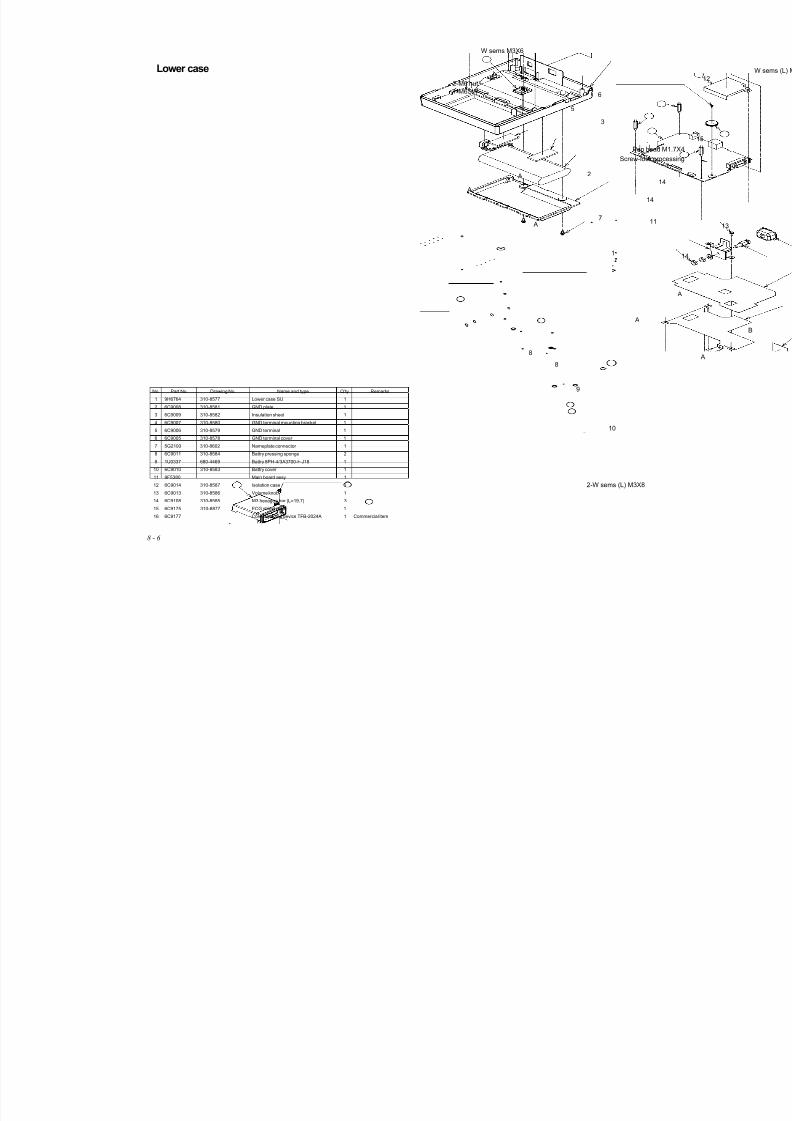
8/13/2019 Manual de Service Fcp-7101 - Fx-7102
http://slidepdf.com/reader/full/manual-de-service-fcp-7101-fx-7102 152/170
8 - 6
Lower case
No. Part No. Drawing No. Name and type Q’ty Remarks
1 9H6764 310-8577 Lower case SU 1
2 6C9008 310-8581 GND plate 1
3 6C9009 310-8582 Insulation sheet 14 6C9007 310-8580 GND terminal mounting bracket 1
5 6C9006 310-8579 GND terminal 1
6 6C9005 310-8578 GND terminal cover 1
7 5G2193 310-8602 Nameplate connector 1
8 6C9011 310-8584 Battry pressing sponge 2
9 1U0337 680-4469 Battry 8PH-4/3A3700-H-J18 1
10 6C9010 310-8583 Battry cover 1
11 9F5380 Main board assy 1
12 6C9014 310-8587 Isolation case 1
13 6C9013 310-8586 Volume knob 1
14 6C9108 310-8585 M3 hexagon bar (L=19.7) 3
15 6C9175 310-8877 ECG shield plate 1
16 6C9177 Core fastening device TFB-2024A 1 Commercial item
6
5
4
3
2
7
1
8
8
9
10
2-M6 nut
1-M6SW
W sems M3X6
16
11
14
14 A
A
A
B
A
2-W sems (L) M3X8
Screw-lock process
Pan head M1.7

8/13/2019 Manual de Service Fcp-7101 - Fx-7102
http://slidepdf.com/reader/full/manual-de-service-fcp-7101-fx-7102 153/170
General assembly diagram (FX-7102)
No. Par t No .
1 410-
2 410-
3 410-
4 410-
5 410-
6 6C9107 310-
7 1L1778 680-
8 5G2194 310-
9 5G2195 310-
10 6C9176 310-
11 1T7094
12 9E9786
LCD section
3-M3 nut,
Screw-lock processing
5 4
e
a
d
bc
2-W sems (L)
M3X8
3
3
11
1
bc
ef
d
a
12
2-W sems
M3X8
8
9
f Folded under GND plate (LCD)
106
7
Assembly of LCD section
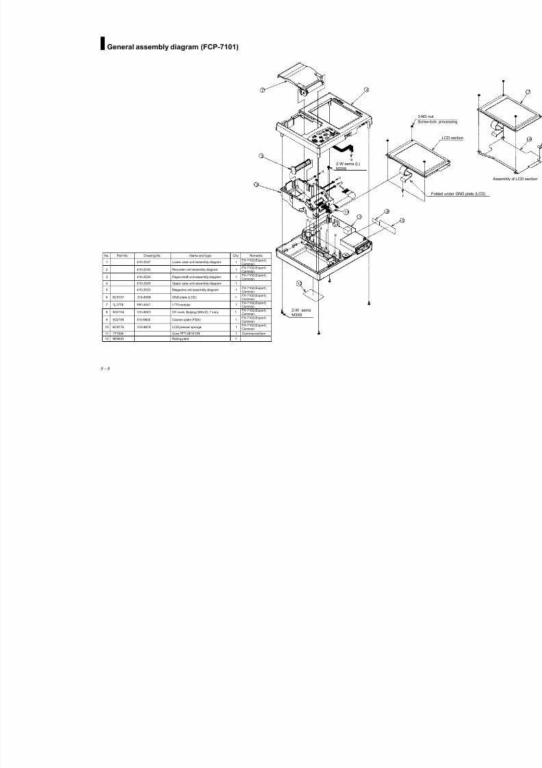
8/13/2019 Manual de Service Fcp-7101 - Fx-7102
http://slidepdf.com/reader/full/manual-de-service-fcp-7101-fx-7102 154/170
8 - 8
General assembly diagram (FCP-7101)
No. Part No. Drawing No. Name and type Q’ty Remarks
1 410-2537 Lower case unit assembly diagram 1FX-7102 (Export)Common
2 410-2535 Recorder unit assembly diagram 1FX-7102 (Export)Common
3 410-2534 Paper shaft unit assembly diagram 1FX-7102 (Export)Common
4 410-2529 Upper case unit assembly diagram 1
5 410-2533 Magazine unit assembly diagram 1FX-7102 (Export)Common
6 6C9107 310-8588 GND plate (LCD) 1FX-7102 (Export)Common
7 1L1778 680-4441 LCD module 1FX-7102 (Export)Common
8 5G2194 310-8603 CE mark: Beijing (With ID, 7 mm) 1FX-7102 (Export)Common
9 5G2195 310-8604 Caution plate (FDA) 1FX-7102 (Export)Common
10 6C9176 310-8878 LCD presser sponge 1FX-7102 (Export)Common
11 1T7094 Core TFT-081813N 1 Commercial item
12 9E9839 Rating plate 1
2-W semsM3X8
3-M3 nut,
Screw-lock processing
LCD sectio
Folded under GN
3
3
5 4
2-W sems (L)
M3X8
e
a
d
b
c
bc
ef
d
a
111
8
9
12
f

8/13/2019 Manual de Service Fcp-7101 - Fx-7102
http://slidepdf.com/reader/full/manual-de-service-fcp-7101-fx-7102 155/170
Outline view (FX-7102)
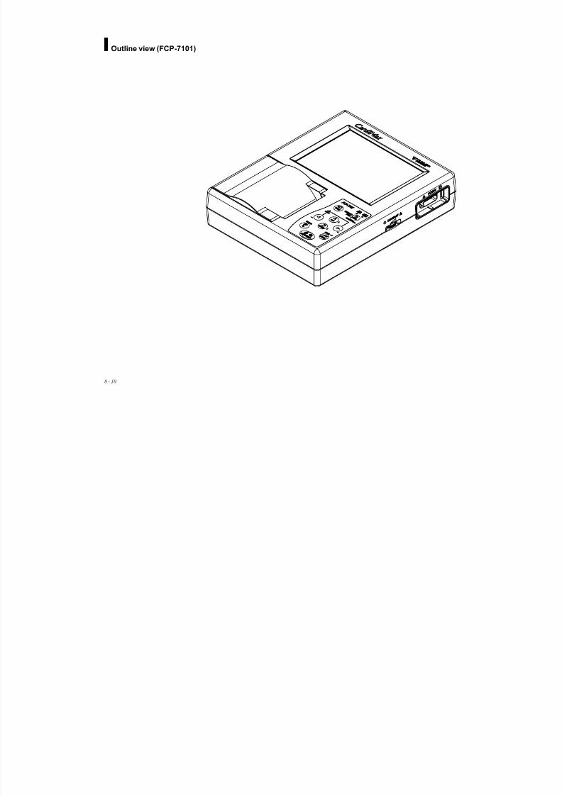
8/13/2019 Manual de Service Fcp-7101 - Fx-7102
http://slidepdf.com/reader/full/manual-de-service-fcp-7101-fx-7102 156/170
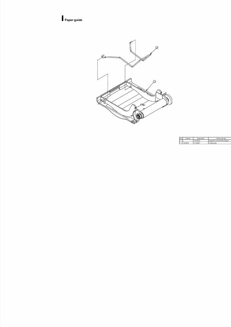
8/13/2019 Manual de Service Fcp-7101 - Fx-7102
http://slidepdf.com/reader/full/manual-de-service-fcp-7101-fx-7102 157/170
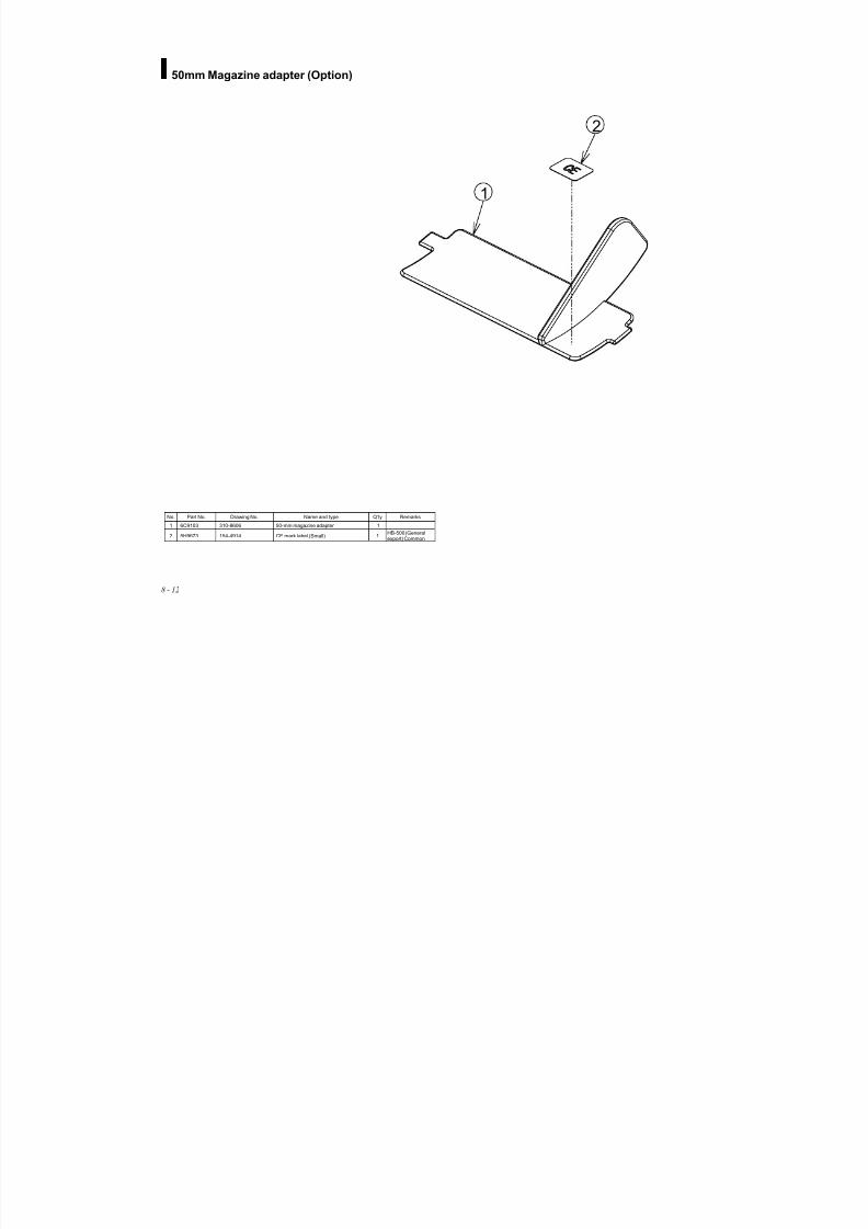
8/13/2019 Manual de Service Fcp-7101 - Fx-7102
http://slidepdf.com/reader/full/manual-de-service-fcp-7101-fx-7102 158/170
8 - 12
50mm Magazine adapter (Option)
1
2
No. Part No. Drawing No. Name and type Q’ty Remarks
1 6C9103 310-8606 50-mm magazine adapter 1
2 5H9673 154-4914 CE mark label (Small) 1HB-500 (Generalexport) Common
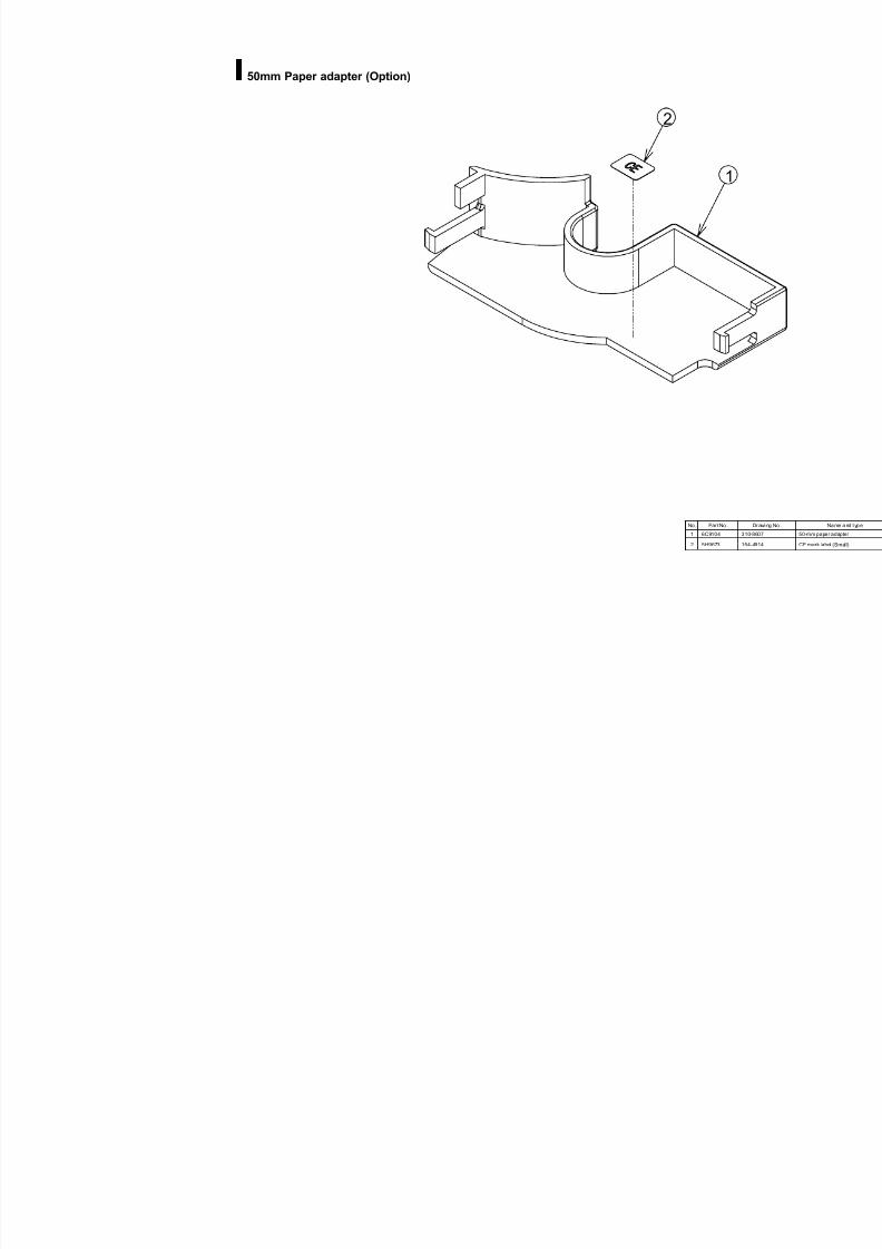
8/13/2019 Manual de Service Fcp-7101 - Fx-7102
http://slidepdf.com/reader/full/manual-de-service-fcp-7101-fx-7102 159/170
50mm Paper adapter (Option)
1
2
No. Par t No .
1 6C9104 310-
2 5H9673 154-

8/13/2019 Manual de Service Fcp-7101 - Fx-7102
http://slidepdf.com/reader/full/manual-de-service-fcp-7101-fx-7102 160/170
8 - 14
8/13/2019 Manual de Service Fcp-7101 - Fx-7102
http://slidepdf.com/reader/full/manual-de-service-fcp-7101-fx-7102 161/170
Chapter 9
Technical Instructions Related toEMC
Emission information CISPR11..........................................................9-2
Immunity information (to other than radiation/conduction)............ 9-3
Immunity information (to radiation/conduction) ..............................9-4
Recommended distance of separation fromportable telephone, etc.......................................................................9-5

8/13/2019 Manual de Service Fcp-7101 - Fx-7102
http://slidepdf.com/reader/full/manual-de-service-fcp-7101-fx-7102 162/170
8/13/2019 Manual de Service Fcp-7101 - Fx-7102
http://slidepdf.com/reader/full/manual-de-service-fcp-7101-fx-7102 163/170
Chapter 9 Technical Instructions Related to EMC
9 - 1
This chapter concerns 4 different information as appended documents
Required by IEC 60601-1-2.
(1) Emission information CISPR11
(2) Immunity information (to other than radiation/conduction)
(3) Immunity information (to radiation/conduction)(4) Recommended distance of separation from portable telephone, etc.
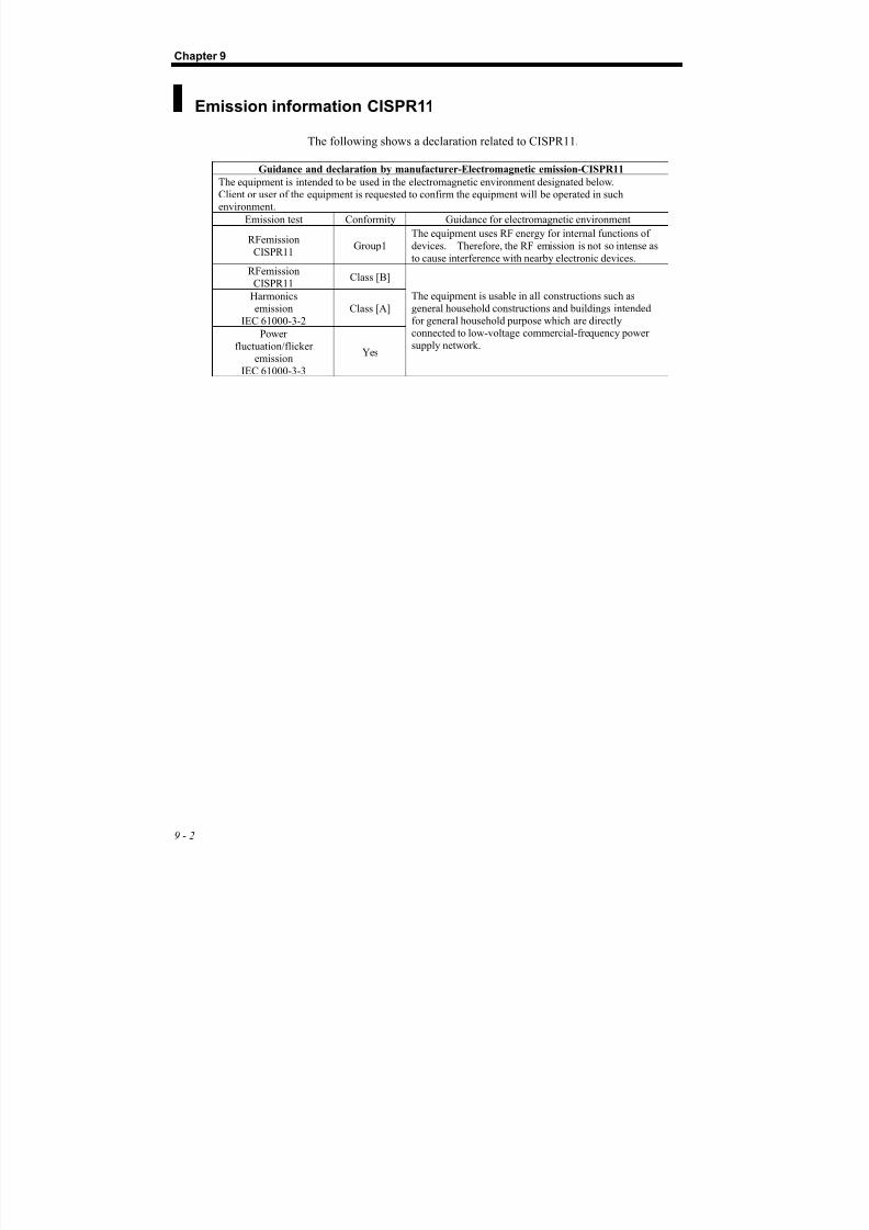
8/13/2019 Manual de Service Fcp-7101 - Fx-7102
http://slidepdf.com/reader/full/manual-de-service-fcp-7101-fx-7102 164/170
Chapter 9
9 - 2
Emission information CISPR11
The following shows a declaration related to CISPR11.
Guidance and declaration by manufacturer-Electromagnetic emission-CISPR11
The equipment is intended to be used in the electromagnetic environment designated below.Client or user of the equipment is requested to confirm the equipment will be operated in suchenvironment.
Emission test Conformity Guidance for electromagnetic environment
RFemission
CISPR11Group1
The equipment uses RF energy for internal functions of
devices. Therefore, the RF emission is not so intense as
to cause interference with nearby electronic devices.
RFemissionCISPR11
Class [B]
Harmonicsemission
IEC 61000-3-2
Class [A]
Power
fluctuation/flickeremission
IEC 61000-3-3
Yes
The equipment is usable in all constructions such as
general household constructions and buildings intendedfor general household purpose which are directlyconnected to low-voltage commercial-frequency power
supply network.
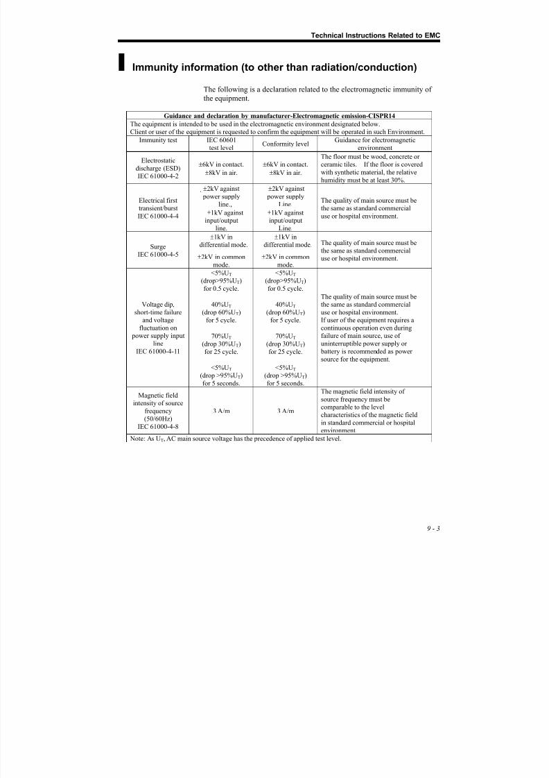
8/13/2019 Manual de Service Fcp-7101 - Fx-7102
http://slidepdf.com/reader/full/manual-de-service-fcp-7101-fx-7102 165/170
Technical Instructions Related to EMC
9 - 3
Immunity information (to other than radiation/conduction)
The following is a declaration related to the electromagnetic immunity of
the equipment.
Guidance and declaration by manufacturer-Electromagnetic emission-CISPR14
The equipment is intended to be used in the electromagnetic environment designated below.Client or user of the equipment is requested to confirm the equipment will be operated in such Environment.
Immunity test IEC 60601test level
Conformity levelGuidance for electromagnetic
environment
Electrostatic
discharge (ESD)IEC 61000-4-2
±6kV in contact.
±8kV in air.
±6kV in contact.
±8kV in air.
The floor must be wood, concrete orceramic tiles. If the floor is covered
with synthetic material, the relative
humidity must be at least 30%.
Electrical firsttransient/burst
IEC 61000-4-4
±2kV against
power supplyline.,
±1kV againstinput/output
line.
±2kV against
power supplyLine.
±1kV againstinput/output
Line.
The quality of main source must bethe same as standard commercial
use or hospital environment.
SurgeIEC 61000-4-5
±1kV indifferential mode.
±2kV in common
mode.
±1kV indifferential mode.
±2kV in common
mode.
The quality of main source must bethe same as standard commercialuse or hospital environment.
<5%UT (drop>95%UT)
for 0.5 cycle.
<5%UT (drop>95%UT)
for 0.5 cycle.
40%UT (drop 60%UT)
for 5 cycle.
40%UT (drop 60%UT)
for 5 cycle.
70%UT
(drop 30%UT)for 25 cycle.
70%UT
(drop 30%UT)for 25 cycle.
Voltage dip,
short-time failureand voltage
fluctuation on power supply input
lineIEC 61000-4-11
<5%UT (drop >95%UT)
for 5 seconds.
<5%UT (drop >95%UT)
for 5 seconds.
The quality of main source must bethe same as standard commercial
use or hospital environment.If user of the equipment requires a
continuous operation even duringfailure of main source, use of
uninterruptible power supply or battery is recommended as power
source for the equipment.
Magnetic fieldintensity of source
frequency(50/60Hz)
IEC 61000-4-8
3 A/m 3 A/m
The magnetic field intensity of
source frequency must becomparable to the levelcharacteristics of the magnetic field
in standard commercial or hospitalenvironment.
Note: As UT, AC main source voltage has the precedence of applied test level.
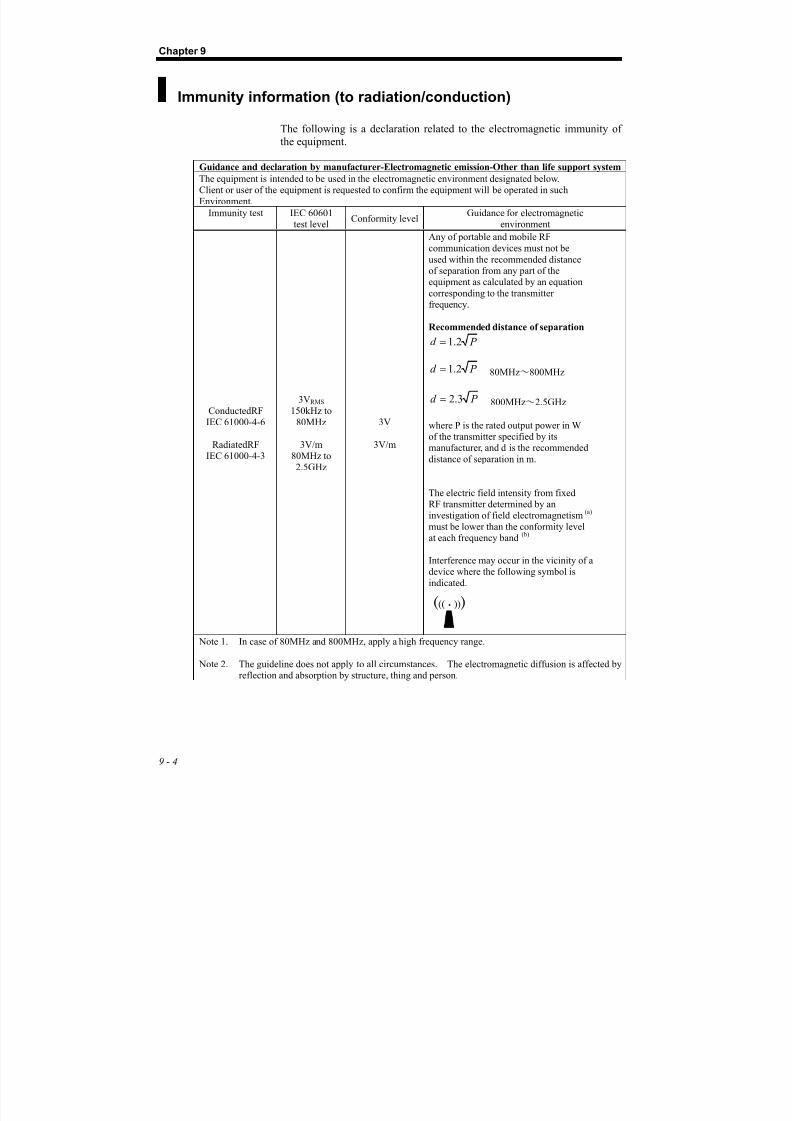
8/13/2019 Manual de Service Fcp-7101 - Fx-7102
http://slidepdf.com/reader/full/manual-de-service-fcp-7101-fx-7102 166/170
Chapter 9
9 - 4
Immunity information (to radiation/conduction)
The following is a declaration related to the electromagnetic immunity of
the equipment.
Guidance and declaration by manufacturer-Electromagnetic emission-Other than life support system
The equipment is intended to be used in the electromagnetic environment designated below.Client or user of the equipment is requested to confirm the equipment will be operated in such
Environment.
Immunity test IEC 60601test level
Conformity levelGuidance for electromagnetic
environment
ConductedRFIEC 61000-4-6
RadiatedRFIEC 61000-4-3
3VRMS
150kHz to80MHz
3V/m80MHz to2.5GHz
3V
3V/m
Any of portable and mobile RF
communication devices must not be
used within the recommended distanceof separation from any part of theequipment as calculated by an equation
corresponding to the transmitterfrequency.
Recommended distance of separation
P d 2.1=
P d 2.1= 80MHz~800MHz
P d 3.2= 800MHz~2.5GHz
where P is the rated output power in Wof the transmitter specified by itsmanufacturer, and d is the recommended
distance of separation in m.
The electric field intensity from fixedRF transmitter determined by aninvestigation of field electromagnetism
(a)
must be lower than the conformity levelat each frequency band
(b)
Interference may occur in the vicinity of adevice where the following symbol is
indicated.
(((・)))
Note 1. In case of 80MHz and 800MHz, apply a high frequency range.
Note 2. The guideline does not apply to all circumstances. The electromagnetic diffusion is affected byreflection and absorption by structure, thing and person.

8/13/2019 Manual de Service Fcp-7101 - Fx-7102
http://slidepdf.com/reader/full/manual-de-service-fcp-7101-fx-7102 167/170
Technical Instructions Related to EMC
9 - 5
a It is impossible to accurately and theoretically estimate the electric field intensity from a stationarysending station such as radio telephone base station (cord-less), local portable radio station, amateur
radio station, AM/FM radio broadcasting station and at TV base station. For correctly judging theenvironment of electromagnetism due to stationary RF sending station, proceed to fieldelectromagnetism investigation. If the electric field intensity recorded at a site where the equipment is
used exceeds the above applied RF conformity level, watch the equipment to verify whether it operates properly or not. If its operation is found abnormal, the equipment may have to be modified to match,
be moved to another place or be subjected to supplementary means. b The electric field intensity must be 3 V/m or less over the entire frequency band of 150 MHz to 80
MHz.
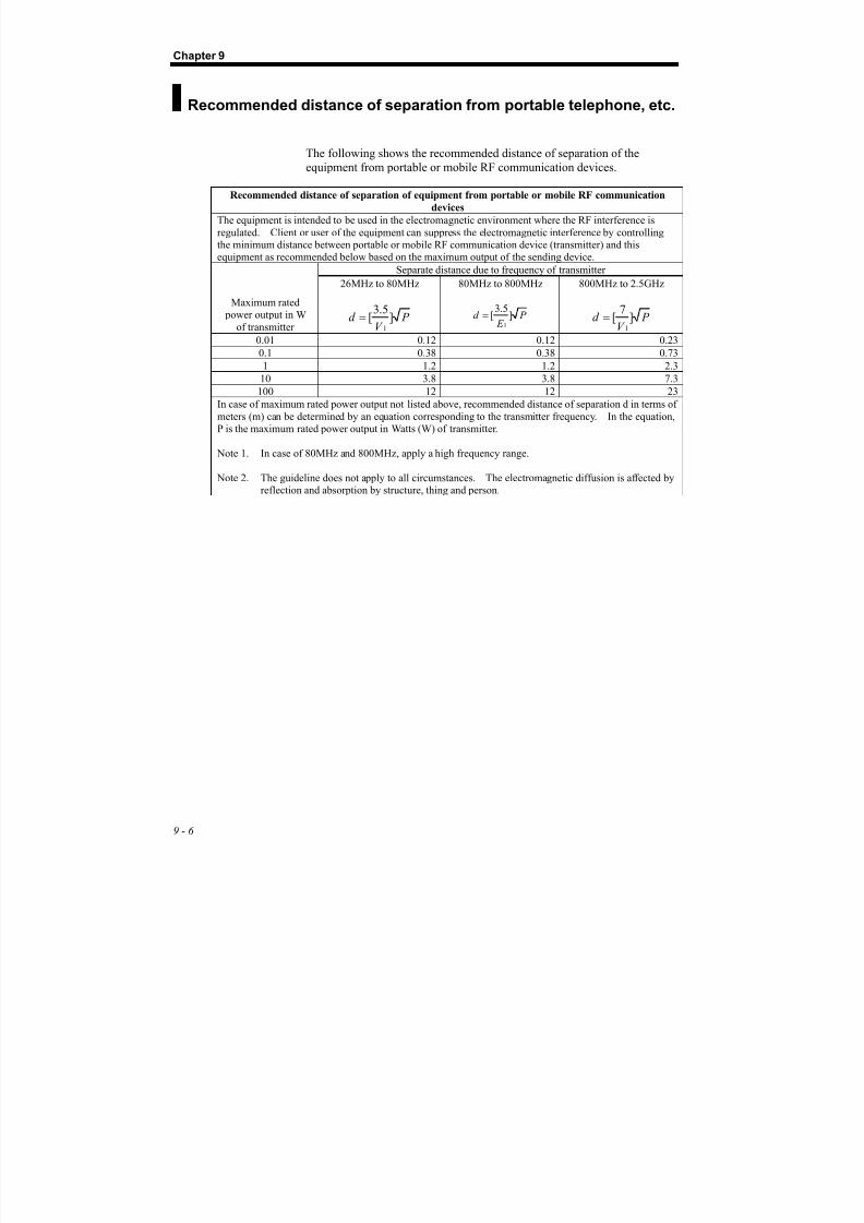
8/13/2019 Manual de Service Fcp-7101 - Fx-7102
http://slidepdf.com/reader/full/manual-de-service-fcp-7101-fx-7102 168/170
Chapter 9
9 - 6
Recommended distance of separation from portable telephone, etc.
The following shows the recommended distance of separation of theequipment from portable or mobile RF communication devices.
Recommended distance of separation of equipment from portable or mobile RF communication
devices
The equipment is intended to be used in the electromagnetic environment where the RF interference is
regulated. Client or user of the equipment can suppress the electromagnetic interference by controllingthe minimum distance between portable or mobile RF communication device (transmitter) and thisequipment as recommended below based on the maximum output of the sending device.
Separate distance due to frequency of transmitter
Maximum rated power output in W
of transmitter
26MHz to 80MHz
P V
d ]5.3
[1
=
80MHz to 800MHz
P E
d ]5.3
[1
=
800MHz to 2.5GHz
P V
d ]7
[1
=
0.01 0.12 0.12 0.23
0.1 0.38 0.38 0.73
1 1.2 1.2 2.3
10 3.8 3.8 7.3
100 12 12 23
In case of maximum rated power output not listed above, recommended distance of separation d in terms of
meters (m) can be determined by an equation corresponding to the transmitter frequency. In the equation,P is the maximum rated power output in Watts (W) of transmitter.
Note 1. In case of 80MHz and 800MHz, apply a high frequency range.
Note 2. The guideline does not apply to all circumstances. The electromagnetic diffusion is affected byreflection and absorption by structure, thing and person.

8/13/2019 Manual de Service Fcp-7101 - Fx-7102
http://slidepdf.com/reader/full/manual-de-service-fcp-7101-fx-7102 169/170

8/13/2019 Manual de Service Fcp-7101 - Fx-7102
http://slidepdf.com/reader/full/manual-de-service-fcp-7101-fx-7102 170/170