market survey technical description planar silicon sensors
TRANSCRIPT
April 2016
MS-4086/EP
Market Survey
Technical Description Planar Silicon Sensors for the ATLAS and
CMS Outer Tracker Upgrades
Abstract This market survey concerns the supply of planar silicon sensors for the ATLAS and CMS Outer Tracker upgrades. It will be followed by the issue of several Invitations to Tender to qualified and selected contractors. ATLAS may split its total requirements into several contracts to be placed by CERN and by participating institutes of the ATLAS experiment through separate Invitations to Tender. The ATLAS Invitation to Tender to be conducted by CERN will be issued in the first quarter of 2017 for a contract to be awarded in the third quarter of 2017. CERN may issue one or two Invitations to Tender for CMS in the first quarter of 2018 for a contract to be awarded in the third quarter of 2018. Furthermore, CERN reserves the right to split the contracts amongst at least two contractors for each of the CMS Invitations to Tender.

i MS-4086/EP
Table of Contents
1 INTRODUCTION ........................................................................................................................... 1 1.1 Introduction to CERN ....................................................................................................................... 1 1.2 Introduction to the ATLAS and CMS Experiments .......................................................................... 2 2 SCOPE OF THIS MARKET SURVEY ........................................................................................ 3 3 DETAILED DESCRIPTION OF THE SUPPLY ......................................................................... 4 3.1 Substrate Material ............................................................................................................................. 4 3.2 Production Process ............................................................................................................................ 4 3.3 Sensor Design and Wafer Layout ...................................................................................................... 5 3.4 Sensor Types and Multiplicities ........................................................................................................ 6 3.5 Operational Environment .................................................................................................................. 8 3.6 Quality Assurance during Production ............................................................................................... 8 4 QUALIFICATION PROCEDURE .............................................................................................. 12 4.1 Step One .......................................................................................................................................... 12 4.2 Step Two ......................................................................................................................................... 12 4.3 Step Three ....................................................................................................................................... 13 5 PERFORMANCE OF THE CONTRACT .................................................................................. 14 5.1 Provisional Delivery Schedule ........................................................................................................ 14 5.2 Contract Follow-up and Progress Monitoring ................................................................................. 15 6 CERN CONTACT PERSONS ..................................................................................................... 16

1 MS-4086/EP
1 INTRODUCTION
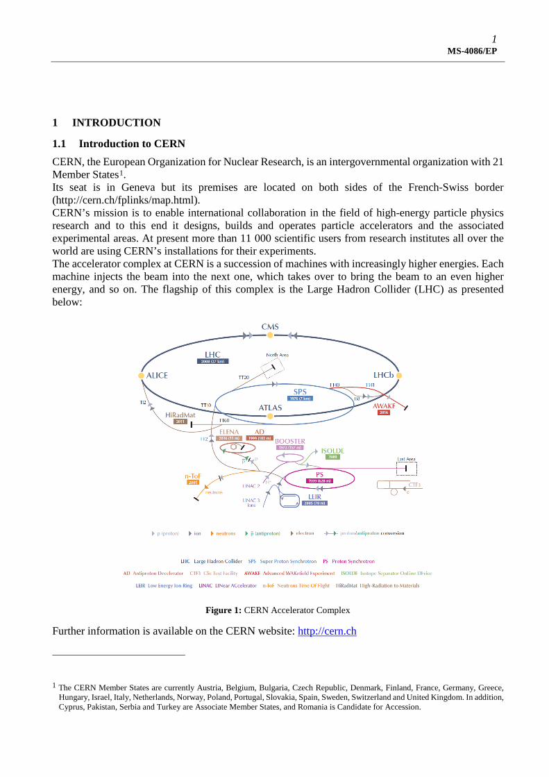
1.1 Introduction to CERN CERN, the European Organization for Nuclear Research, is an intergovernmental organization with 21 Member States1. Its seat is in Geneva but its premises are located on both sides of the French-Swiss border (http://cern.ch/fplinks/map.html). CERN’s mission is to enable international collaboration in the field of high-energy particle physics research and to this end it designs, builds and operates particle accelerators and the associated experimental areas. At present more than 11 000 scientific users from research institutes all over the world are using CERN’s installations for their experiments. The accelerator complex at CERN is a succession of machines with increasingly higher energies. Each machine injects the beam into the next one, which takes over to bring the beam to an even higher energy, and so on. The flagship of this complex is the Large Hadron Collider (LHC) as presented below:
Figure 1: CERN Accelerator Complex
Further information is available on the CERN website: http://cern.ch
1 The CERN Member States are currently Austria, Belgium, Bulgaria, Czech Republic, Denmark, Finland, France, Germany, Greece,
Hungary, Israel, Italy, Netherlands, Norway, Poland, Portugal, Slovakia, Spain, Sweden, Switzerland and United Kingdom. In addition, Cyprus, Pakistan, Serbia and Turkey are Associate Member States, and Romania is Candidate for Accession.
2 MS-4086/EP
1.2 Introduction to the ATLAS and CMS Experiments ATLAS, or A Toroidal LHC ApparatuS (www.atlas.ch) is a particle physics experiment at the Large Hadron Collider (LHC) at CERN. The ATLAS detector is designed and constructed to make new particle discoveries resulting from head-on collisions of protons produced by the LHC of extraordinarily high energy. ATLAS will investigate the basic forces that have shaped our Universe since the beginning of time and that will determine its fate. Among the possible discovery candidates are particles that could explain the origin of mass, confirm the existence of extra dimensions in space, unification of fundamental forces, and evidence of dark matter in our Universe. The ATLAS detector is located in an underground cavern on the Swiss part of CERN. The experiment is in operation and produces physics results. The ATLAS collaboration involves 3000 scientists from 174 institutions in 38 countries. The Compact Muon Solenoid, or CMS (http://cms.cern.ch), is a particle physics experiment at the Large Hadron Collider (LHC) at CERN. The CMS detector is designed to study particles produced in high-energy proton-proton and heavy ion collisions to seek answers to fundamental questions such as: “understanding why the world is the way it is, why some particles weigh more than others and what constitutes the dark matter in the Universe”. The CMS detector is located 100 m underground at the French village of Cessy near Geneva. The experiment is in operation and the data now being collected by CMS is distributed to institutes around the world to be analysed. The CMS collaboration involves more than 4300 particle physicists, engineers, technicians, students and support staff from 179 universities and institutes in 41 countries.

3 MS-4086/EP
2 SCOPE OF THIS MARKET SURVEY The purpose of this market survey is to identify potential bidders for the supply of high quality radiation tolerant planar silicon strip sensors (hereafter referred to as the sensors). The sensors will be used in the outer tracking detectors of the ATLAS and CMS experiments (hereafter referred to as the experiments). The requirements from both experiments are largely similar. For some of the main specifications, like wafer material and thickness, the preferred choices are different. The final requirements of the technical specification will be finalised using the information gathered from this market survey. Each of the two detectors requires more than 200 m2 of planar silicon sensors produced on 6” (150mm) or 8” (200 mm) wafers from p-type float-zone (FZ) or magnetic Czochralski (mCZ) material. In ATLAS, AC-coupled strip sensors are the baseline but DC-coupled sensors are also being investigated. Most of the CMS sensors (85%) are AC-coupled strip sensors while a small fraction of the supply will be in DC-coupled technology. Details, like sensor geometries and the final electrical requirements will be different for ATLAS and CMS and will depend on the technology used. Therefore, separate Invitations to Tender will be issued for ATLAS and CMS following this market survey:
- CERN may issue separate Invitations to Tender for each sensor technology for CMS. Furthermore, CERN reserves the right to split the contracts among at least two contractors for each of the CMS Invitations to Tender;
- ATLAS may split its total requirements into several contracts, to be placed by CERN and by participating institutes of the ATLAS experiment through separate Invitations to Tender.
Only firms qualified and selected by CERN after analysis of their reply to this market survey and successful completion of the qualification procedure defined in section 4, will be included in the forthcoming Invitations to Tender. The supply shall originate from the CERN1 Member States and under certain conditions from Associate Member States or Candidates for Accession or from the ATLAS2 or CMS3 Member States.
2 List of ATLAS Member States: Argentina, Armenia, Australia, Austria, Azerbaijan Republic, Republic of Belarus, Brazil, Canada,
Chile, China, Colombia, Czech Republic, Denmark, France, Georgia, Germany, Greece, Israel, Italy, Japan, Morocco, Netherlands, Norway, Poland, Portugal, Romania, Russia, Serbia, Slovak Republic, Slovenia, South Africa, Spain, Sweden, Switzerland, Taiwan, Turkey, United Kingdom, USA
3 List of CMS Member States: Austria, Belgium, Brazil, Bulgaria, China, Colombia, Croatia, Cyprus, Czech Republic, Egypt, Estonia, Finland, France, Germany, Greece, Hungary, India, Iran, Ireland, Italy, South Korea, Lithuania, Malaysia, Mexico, New Zealand, Pakistan, Poland, Portugal, Russia, Serbia, Spain, Switzerland, Taiwan, Thailand, Turkey, United Kingdom, USA

4 MS-4086/EP
3 DETAILED DESCRIPTION OF THE SUPPLY
3.1 Substrate Material The sensors shall be produced on either 6” (150mm) or 8” (200 mm) wafers. The current baseline designs of the ATLAS and CMS Outer Trackers upgrades are optimized for sensors cut from 6” wafers but could be adapted for larger sensors cut from 8” wafers. The main benefit expected is a reduction of cost per active sensor area. Substrates shall be high resistive p-type wafers produced either in FZ or mCZ technology with a crystal orientation of <100>. While ATLAS’s default is FZ and CMS prefers mCZ, the availability of both materials is of interest for each of the two experiments. The physical thickness of the sensors shall be either 200-220 µm (thin sensors) or 300-320 µm (thick sensors), as shown in the table below, with CMS having a preference for thin sensors. Furthermore, for thick sensors, CMS is interested in substrates with a reduced active thickness compared to the physical thickness. Technologies which can provide such substrates shall be investigated by CMS before they can be considered as an alternative for the Invitations to Tender. Previous investigations have shown that deep diffused FZ (ddFZ) wafers with an active thickness of 200 µm and a physical thickness of 320 µm, can provide acceptable performance and radiation tolerance. Therefore, ddFZ is considered an accepted technology and included as a possible substrate material for CMS.
Summary: Substrate Material ATLAS CMS Size 8”/200 mm or 6”/150 mm Type p-type FZ p-type FZ/ddFZ4/MCz Crystal orientation <100> Thickness (physical) 200-220/300-320 µm Thickness (active) >= 90% of physical thickness 200/300 µm Thickness tolerance ± 5 % Resistivity > 3 kΩcm Oxygen concentration 1 x 10¹⁶ – 7 x 1017 cm-3 < 2 x 1016 cm-3 (FZ)
≈ 1 x 1017 cm-3 (dd-FZ) 5 ≈ 5 x 1017 cm-3 (MCz)5
Table 1
3.2 Production Process The development of a stable production process, which satisfies all the technical requirements stated in this document, is the responsibility of the selected supplier(s). Both experiments will provide help in the development by characterising prototype sensors and test structures and sharing the measurement results with the potential supplier(s). The final production process shall be validated by each of the experiments according to the qualification procedure described in section 4.
3.2.1 AC-coupled strip sensors The default sensor type of all of the ATLAS and most of the CMS sensors can be categorised as AC-coupled strip sensors. ATLAS is also investigating a design with DC-coupled sensors. In case this 4 Deep Diffusion FZ: Reduction of the active thickness by deep diffusion from the backside of the wafer 5 Variation of [O] should be within 50 % and 200 % of the specified value

5 MS-4086/EP
technology is chosen by ATLAS for production, the specifications concerning the coupling capacitance will be void, while all other parameters and requirements remain unchanged. Strips shall be n-type implants capacitively coupled to a metal readout strip. The dielectric between implant and readout strip shall be thin to enable a high capacitance while being electrically and mechanically stable. The capacitor formed by the implant and readout strips shall provide a high breakdown voltage as specified later. Each implant strip shall be connected to a common bias line using a polysilicon resistor. The strip isolation can be achieved either with p-stop implants and/or p-spray technology. The contact pads shall be able to withstand probing with standard probe needles during the quality assurance measurements. The connection to the readout chips will be done using standard ultrasonic aluminium wire bonding, therefore the pads shall be compatible with this technology (> 10 g pull force per bond). High voltage stability and low current operation of the sensors shall be ensured using guard ring(s) and an appropriate sensor periphery which may include a p+ edge implant to protect the active sensor area from damage at the cutting edge. The backside of the sensors shall be covered by a uniform metallisation with a good ohmic contact to the bulk of the sensor using a p+ implant. The frontside shall be passivated with the exception of the contact and wire-bonding pads of the implant and readout strips and parts of the bias and guard rings.
3.2.2 DC-coupled macro-pixel sensors These sensors are only relevant for CMS. They consist of 1.5 mm long n-type pixels at a pitch of 100 µm. The DC-coupled pixel implants are directly read out. Each pixel shall be connected to a biasing grid using punch-through structures which are mainly foreseen for testing purposes. During normal operation, each pixel will be biased through the readout chip. The isolation of the pixels shall be done either with p-stop implants and/or p-spray technology. These sensors will be bump bonded to an ASIC of which 6 chips are needed to cover the full 5 x 10 cm2 sensor. The contact pads shall be compatible with the requirements of this process, which concerns mainly the application of an under-bump metalisation (UBM). It is assumed, that the UBM will not be performed by the contractor(s). The full specifications for the bump bonding technology that will be used are not yet decided.
3.3 Sensor Design and Wafer Layout The design of the sensors including the full layout of the wafers can either be provided by the experiments in the form of GDSII files or it shall be the responsibility of the contractor(s) following the detailed technical specifications of the Invitations to Tenders for ATLAS and CMS. In the former case, the responsibility to ensure the compatibility of the masks with the contractor’s process shall remain with the contractor(s). All relevant information to properly implement the designs (design rules) shall be shared with the experiments. In the latter case, the contractor(s) shall be responsible for providing a design that is sufficiently radiation tolerant up to 2 x 10¹⁵ neq/cm² (collected cluster charge above 7500 electrons per MIP at 500 V, no non-Gaussian noise contributions) and shall fulfil all requirements described in section 3.6. The contractor(s) shall choose which procedure they want to follow at the beginning of step 3 of the qualification procedure described in section 4. Each wafer will consist of one to three sensors covering most of the area of the wafer. The remaining space will be filled with various test structures, which will be used within the experiments for quality assurance (QA). The contractor(s) may utilize these structures for in-house QA as well and/or add their own test structures. The contractor(s) shall deliver all sensors which pass the requirements to CERN, together with the test structures which reside on the same wafer.
6 MS-4086/EP
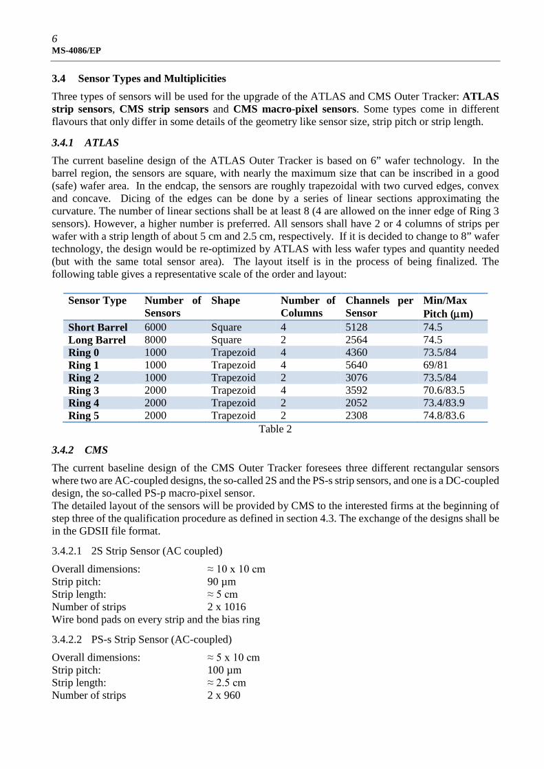
3.4 Sensor Types and Multiplicities Three types of sensors will be used for the upgrade of the ATLAS and CMS Outer Tracker: ATLAS strip sensors, CMS strip sensors and CMS macro-pixel sensors. Some types come in different flavours that only differ in some details of the geometry like sensor size, strip pitch or strip length.
3.4.1 ATLAS The current baseline design of the ATLAS Outer Tracker is based on 6” wafer technology. In the barrel region, the sensors are square, with nearly the maximum size that can be inscribed in a good (safe) wafer area. In the endcap, the sensors are roughly trapezoidal with two curved edges, convex and concave. Dicing of the edges can be done by a series of linear sections approximating the curvature. The number of linear sections shall be at least 8 (4 are allowed on the inner edge of Ring 3 sensors). However, a higher number is preferred. All sensors shall have 2 or 4 columns of strips per wafer with a strip length of about 5 cm and 2.5 cm, respectively. If it is decided to change to 8” wafer technology, the design would be re-optimized by ATLAS with less wafer types and quantity needed (but with the same total sensor area). The layout itself is in the process of being finalized. The following table gives a representative scale of the order and layout:
Sensor Type Number of Sensors
Shape Number of Columns
Channels per Sensor
Min/Max Pitch (µm)
Short Barrel 6000 Square 4 5128 74.5 Long Barrel 8000 Square 2 2564 74.5 Ring 0 1000 Trapezoid 4 4360 73.5/84 Ring 1 1000 Trapezoid 4 5640 69/81 Ring 2 1000 Trapezoid 2 3076 73.5/84 Ring 3 2000 Trapezoid 4 3592 70.6/83.5 Ring 4 2000 Trapezoid 2 2052 73.4/83.9 Ring 5 2000 Trapezoid 2 2308 74.8/83.6
Table 2
3.4.2 CMS The current baseline design of the CMS Outer Tracker foresees three different rectangular sensors where two are AC-coupled designs, the so-called 2S and the PS-s strip sensors, and one is a DC-coupled design, the so-called PS-p macro-pixel sensor. The detailed layout of the sensors will be provided by CMS to the interested firms at the beginning of step three of the qualification procedure as defined in section 4.3. The exchange of the designs shall be in the GDSII file format.
3.4.2.1 2S Strip Sensor (AC coupled)
Overall dimensions: ≈ 10 x 10 cm Strip pitch: 90 µm Strip length: ≈ 5 cm Number of strips 2 x 10¹⁶ Wire bond pads on every strip and the bias ring
3.4.2.2 PS-s Strip Sensor (AC-coupled) Overall dimensions: ≈ 5 x 10 cm Strip pitch: 100 µm Strip length: ≈ 2.5 cm Number of strips 2 x 960

7 MS-4086/EP
Wire bond pads on every strip and the bias ring
3.4.2.3 PS-p Macro-Pixel Sensor (DC-coupled)
Overall dimensions: ≈ 5 x 10 cm Pixel width: 100 µm Pixel length: ≈ 1.5 mm Number of pixels 32 x 960 Bump bond pads on every pixel and the bias ring CMS is currently studying two layouts for the CMS Outer Tracker with slightly different requirements in terms of the number of PS strip and macro-pixel sensors. Table 1 shows estimates of the required number of sensors for all sensors in each of these two layouts.
Layout 1 Layout 2
2S PS 2S PS
Strip Pixel Strip Pixel
N of modules 8424 7084 8424 5748
N of sensors 16848 7084 7084 16848 5748 5748
N of sensors with spares 19400 8150 8500 19400 6600 6900
Table 3: Quantity of sensors for the two different proposed layouts of the CMS Tracker
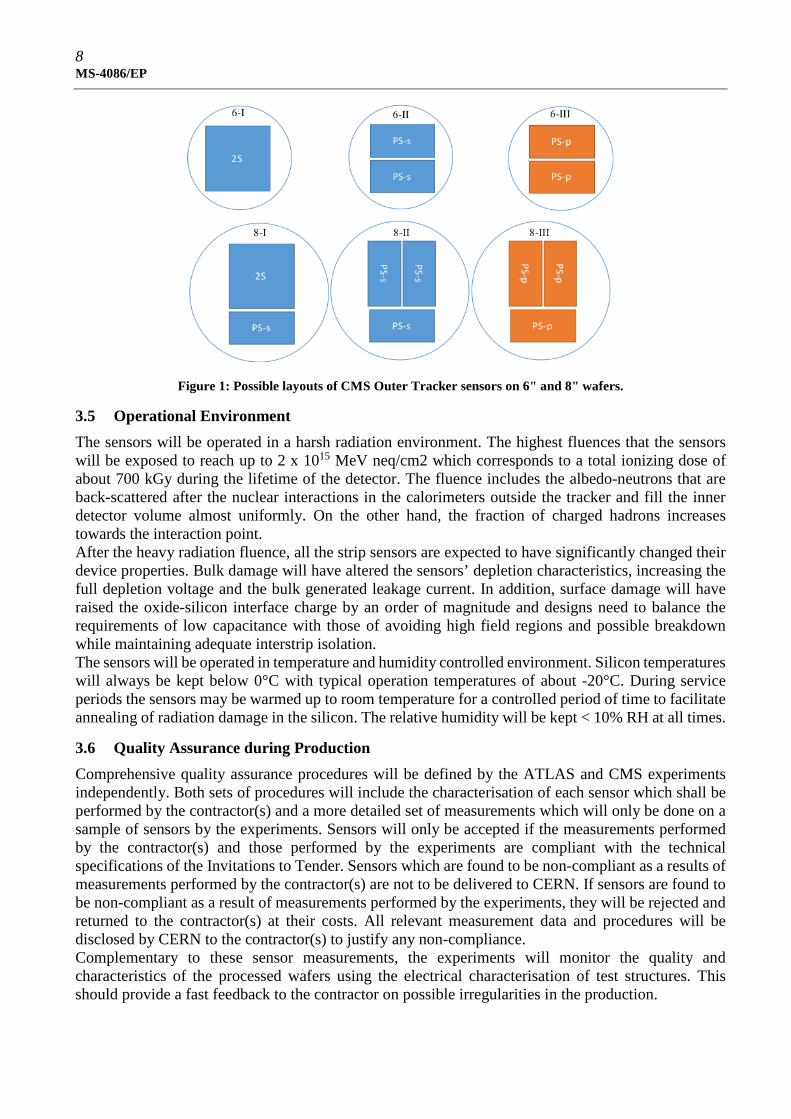
The sensors shall be produced with 6” or 8” technology. To use the available space as efficiently as possible, different wafer layouts are suggested in Figure 1. A mixture of productions in 6” and 8” technology by each contractor or amongst all contractors is acceptable as long as the target values for each sensor type are met as shown in 3.
8 MS-4086/EP
Figure 1: Possible layouts of CMS Outer Tracker sensors on 6" and 8" wafers.
3.5 Operational Environment The sensors will be operated in a harsh radiation environment. The highest fluences that the sensors will be exposed to reach up to 2 x 10¹⁵ MeV neq/cm2 which corresponds to a total ionizing dose of about 700 kGy during the lifetime of the detector. The fluence includes the albedo-neutrons that are back-scattered after the nuclear interactions in the calorimeters outside the tracker and fill the inner detector volume almost uniformly. On the other hand, the fraction of charged hadrons increases towards the interaction point. After the heavy radiation fluence, all the strip sensors are expected to have significantly changed their device properties. Bulk damage will have altered the sensors’ depletion characteristics, increasing the full depletion voltage and the bulk generated leakage current. In addition, surface damage will have raised the oxide-silicon interface charge by an order of magnitude and designs need to balance the requirements of low capacitance with those of avoiding high field regions and possible breakdown while maintaining adequate interstrip isolation. The sensors will be operated in temperature and humidity controlled environment. Silicon temperatures will always be kept below 0°C with typical operation temperatures of about -20°C. During service periods the sensors may be warmed up to room temperature for a controlled period of time to facilitate annealing of radiation damage in the silicon. The relative humidity will be kept < 10% RH at all times.
3.6 Quality Assurance during Production Comprehensive quality assurance procedures will be defined by the ATLAS and CMS experiments independently. Both sets of procedures will include the characterisation of each sensor which shall be performed by the contractor(s) and a more detailed set of measurements which will only be done on a sample of sensors by the experiments. Sensors will only be accepted if the measurements performed by the contractor(s) and those performed by the experiments are compliant with the technical specifications of the Invitations to Tender. Sensors which are found to be non-compliant as a results of measurements performed by the contractor(s) are not to be delivered to CERN. If sensors are found to be non-compliant as a result of measurements performed by the experiments, they will be rejected and returned to the contractor(s) at their costs. All relevant measurement data and procedures will be disclosed by CERN to the contractor(s) to justify any non-compliance. Complementary to these sensor measurements, the experiments will monitor the quality and characteristics of the processed wafers using the electrical characterisation of test structures. This should provide a fast feedback to the contractor on possible irregularities in the production.

9 MS-4086/EP
Measurements to be performed and specifications to be respected for step 3 of the qualification procedure as described in section 4.3 are stated below. These measurements and specifications are subject to change for the Invitations to Tender.
3.6.1 Electrical Specifications by ATLAS Electrical measurements to be performed by the contractor(s) on each sensor (except where otherwise stated). Only sensors fulfilling the electrical requirements will be accepted.
3.6.1.1 Specifications for quality assurance
Electrical measurements to be performed by the contractor on each sensor (except where otherwise stated).
• Full depletion voltage: < 330 V (preference for < 150 V) • Maximum operating voltage: 600 V • Poly-silicon bias resistors: 1-2 MOhm • Inter-strip resistance: > 10 x Rbias at 300 V at 23 C • Inter-strip capacitance: < 1 pF/cm at 300 V, measured at 100 kHz • Coupling capacitance: > 20pF/cm at 1 kHz • Resistance of readout Al strips: < 15 Ohm/cm • Resistance of n-implant strip: < 20 kOhm/cm • Onset of micro-discharge at > 600 V (preferred) • Total initial leakage current,
including guard ring: < 0.1 µA/cm2 at 600 V at room temperature • Number of strip defects < 1% per strip/segment and < 1% per sensor (due
to dielectric punch-through, metal and implant strip defects (opens and shorts), micro-discharging strip or bias resistor failures)
3.6.1.2 Measurements after irradiation
Sensors shall fulfil the following requirements after being subjected to irradiation with ionizing and non-ionizing radiation to a fluence of up to 2×10¹⁵neq/cm² (60 Mrad). Irradiations and the subsequent measurements will be performed by ATLAS. Measurements are performed at T = -20°C.
• Onset of micro-discharge at > 600 V or Vfd + 50 V after irradiation (if lower) • Inter-strip resistance: > 10 x Rbias at 400 V and for T = -20°C • Collected charge > 7500 electrons per MIP at 500V
3.6.1.3 Measurements on dedicated test structures for strip sensors
Dedicated test structures designed by ATLAS will be placed in the free space around the sensors on each wafer which will include a number of miniature (fewer and shorter strip) versions of the main strip sensor for post-irradiation studies. All test structures from wafers with accepted sensors shall be sent to ATLAS. Structures will be characterised on a sampling basis by ATLAS to verify uniformity and conformity of processing parameters including those which influence post-radiation performance.
3.6.1.4 Mechanical Specifications and Optical Inspection
Dicing precision: < ±20 µm or better (deviation of cut from specified dicing line)
Sensor bow after process and dicing: < 200 µm
10 MS-4086/EP
3.6.2 Electrical Specifications by CMS Electrical measurements to be performed by the contractor(s) on each sensor (except where otherwise stated). Only sensors fulfilling all the electrical requirements will be accepted.
3.6.2.1 Environmental conditions Environmental conditions shall be monitored and documented during measurements and shall be within the following range: Temperature: 22˚C ± 4˚C Humidity: < 50% rH
3.6.2.2 Global measurements on sensors
Extracted from I-V and C-V curves on the full sensor (bias voltage between bias ring and backplane) from 0 V – 700 V. The specifications shall be respected regardless if the sensor is pushed flat onto a vacuum chuck or not. Full depletion voltage Vfd: < 150 V @ 200 µm active thickness < 300 V @ 300 µm active thickness Current @500V I500: ≤ 2.5 nA/mm3 (< 5 µA for 100 x 100 x 0.2 mm) Breakdown voltage Vbreak > 700 V, I700 < 3 x I500 Longterm stability6: |ΔI500/I500|< 30% in 48 h @ 500 V bias
3.6.2.3 Measurements on each strip
This subsection only applies to CMS strip sensors! Measurements shall be performed by the contractor (except where otherwise stated) on each strip of a sensor at Vbias = 350 V. The specifications shall be respected regardless if the sensor is pushed flat onto a vacuum chuck or not. Strip current Istrip: < 2 nA/cm Bias resistor Rpoly
median(Rpoly): 1.5 ± 0.3 MΩ (calculated for each sensor) Rpoly: median(Rpoly) ± 5% (for each strip with respect to the
median of the corresponding sensor) Coupling capacitance Cac: > 1.2 pF/cm µm (LCR settings: < 1 V and 1 kHz) Interstrip resistance Rint: > 10 GΩcm (strip to one nearest neighbour) Interstrip capacitance Cint,total: < 1 pF/cm (strip to one nearest neighbour,
LCR settings: < 1 V and 1 MHz) Pinhole check: Idiel < 1 nA@10 V Additionally, strips shall not be: Shorts: Strip implant or aluminium readout is short-circuited with
any of its neighbours Opens: Bond pad does not achieve contact to the full length of its
readout strip If any of these requirements are not met, a strip is considered as bad. A sensor is still accepted if all of the following is fulfilled: Number of bad strips: < 0.5 % per sensor Clustering of bad strips: not more than two bad strips within any cluster of five
consecutive strips 6 Not to be measured by the contractor; Measurements done by CMS on a sample basis

11 MS-4086/EP
3.6.2.4 Measurements on each pixel
This subsection only applies to CMS macro-pixel sensors! Per pixel measurements will only be performed on a sample of sensors by CMS at Vbias = 350 V. The specifications shall be respected regardless if the sensor is pushed flat onto a vacuum chuck or not. Pixel current Ipixel: < 300 pA/pixel Interpixel resistance Rint: > 1 GΩ to each neighbouring pixel Additionally, pixels shall not be: Shorts: Pixel implant or aluminium readout is short-circuited with
any of its neighbours If any of these requirements are not met, a pixel is considered as bad. A sensor is still accepted if all the following is fulfilled: Number of bad pixels: < 0.2 % per sensor Clustering of bad pixels: not more than two bad pixels within any cluster of 4 x 4
pixels
3.6.2.5 Measurements after irradiation
Sensors shall fulfil the following requirements after being subjected to irradiation with ionizing and non-ionizing radiation of a fluence of F ≥ 5e14neq/cm². Measurement are performed at T = -20°C (±2°C). Irradiations and the subsequent measurements will be performed by CMS only. Breakdown voltage Vbreak > 1000 V, I1000 < 4 x I700 Interstrip resistance Rint: > 100 MΩ
3.6.2.6 Measurements on dedicated test structures
Dedicated test structures designed by CMS will be placed in the free space around the sensors on each wafer. All the test structures defined by CMS from wafers with accepted sensors shall be sent to CMS. Structures will be characterised on a sampling basis by CMS only. Strip implant Rstrip: < 250 Ω/square Aluminium strip Ralu: < 25 mΩ/square Dielectric breakdown Vdiel: > 150 V (Idiel < 10 nA@150 V)
3.6.2.7 Mechanical Specifications and Optical Inspection
Dicing precision: < ±10 µm (deviation of cut from specified dicing line) Sensor bow after process/dicing: < 200 µm (6” and 8”)
3.6.2.8 Miscellaneous
• Bond pads compatible with standard wire bond technology o Pull strength > 10 g
• No stains or residues from unspecified chemicals or reactions • No scratches • No chips at the sensors edges larger 20 µm
12 MS-4086/EP
4 QUALIFICATION PROCEDURE A three-step qualification procedure is foreseen to qualify a firm during this market survey. A firm has to successfully qualify each sensor type for a step before the qualification procedure for the subsequent step can be initiated. Only firms which are fully qualified for all three steps are eligible to receive an Invitation to Tender for the mass production of the respective sensor type. The qualification of all three steps shall be concluded before the market survey is closed. Firms providing sensors which have not passed the full qualification procedure before the closure of the market survey shall be considered as non-qualified and shall not be eligible to receive the subsequent Invitations to Tender.
4.1 Step One The qualification of the first step is based on the documents returned by the firm as reply to the technical questionnaire of this market survey. The response time is four weeks from the date of issue of the market survey. Based on the qualification criteria defined in the corresponding document, only firms that fulfil all requirements can be qualified. Firms can be qualified in step one for each type of sensor (ATLAS strip sensors, CMS strip sensors or CMS macro-pixel sensors) or any combination of the three. Only firms which successfully pass the qualification of step one for a certain sensor type will be requested to participate in step two for the corresponding sensor type.
4.2 Step Two To get a first indication of the quality a firm is capable of delivering, a small number (10 – 20 pcs) of sensor samples will be requested free of charge to CERN. The samples shall be delivered to CERN not later than four weeks after the request has been made by CERN. These samples shall be fully functional sensors, which are representative of the quality the firm is able to achieve. The samples shall be accompanied by detailed data sheets of the samples and include documentation on their intended or actual application. The sensors can be from a previous production for an arbitrary project and can therefore deviate from the sensors defined in this document in design and material. Nevertheless, they should be reasonably similar in functionality to enable a reasonable assessment. The minimum specifications the samples shall fulfil are:
• Wafer diameter: 6” or 8” • Resistivity: > 3 kΩcm • Physical thickness: ≤ 350 µm • Size: ≥ 4 cm2
To qualify for ATLAS and/or CMS strip sensors: • AC-coupled strips with polysilicon resistor biasing
To qualify for CMS macro-pixel sensors: • DC-coupled pixels or small strips with punch-through biasing
The samples will be evaluated within both experiments by conducting electrical characterisations before and after irradiation. The samples are not expected to fulfil all the electrical requirements described in section 3.6. Nevertheless, the sample shall comply with the following minimum requirements:
13 MS-4086/EP
Full depletion voltage Vdepl: within 20% of Vdepl calculated from the resistivity of the bulk material and its thickness as originally specified for this sample7
Maximum operating voltage: ≥ 400 V Total initial leakage current: < 10 nA/mm3 at 300 V at room temperature Polysilicon bias resistors8: within ± 20% of the value originally specified for this sample Interstrip/pixel resistance: > 1 GΩ (to each neighbour) Dielectric breakdown Vdiel8: > 100 V (Idiel < 10 nA@100 V) Number of defect strips/pixel: < 1% per sensor (due to dielectric punch-through, metal or implant
defects (opens and shorts), micro-discharges or bias resistor failures)
Firms can be qualified in step two for each type of sensor (ATLAS strip sensors, CMS strip sensors or CMS macro-pixel sensors) or any combination of the three. Only firms which successfully pass the qualification of step two for a certain sensor type will be requested to participate in step three for the corresponding sensor type.
4.3 Step Three The final qualification step requires the production of full-size and fully featured prototype sensors of a sensor type, according to the specifications stated in section 3 of this document. The number of sensors shall be sufficient to conduct all necessary characterisations and will be defined by the ATLAS and CMS experiments. The number of sensors is expected to be in the order of 20 wafers each consisting of the same sensors and test structures. To initiate this step, CERN shall request an offer from each firm eligible to participate in step 3 and, upon acceptance of the offer, issue a purchase order with the firm concerned. It should be noted that the total amount of all orders within step 3 must remain within the funds allocated by the experiments for step 3. CERN shall accept and pay for each prototype sensor which complies with the specifications stated in section 3 of this document. Furthermore, the orders for step 3 shall not be placed later than Q4 2016. The sensors required to qualify for step 3 shall not be delivered to CERN later than nine months after placement of the order by CERN. All compliant sensors will be electrically characterised before and after irradiation by the experiments. A fraction of the sensors will be used to build fully functional detector modules, which will then be tested in beam tests by the experiments. The prototype sensors shall fulfil all the specifications stated in section 3 of this document, before a firm is qualified for the corresponding sensor type. Firms can be qualified in step three for each type of sensor (ATLAS strip sensors, CMS strip sensors or CMS macro-pixel sensors) or any combination of the three. The qualification is only valid for the specific production process used to manufacture the samples provided in step three. Any changes to the process afterwards shall be documented and communicated to CERN in writing beforehand. It is at the discretion of the experiments to decide, if a requalification of step three for the modified process is necessary. Only firms which have successfully passed the qualification of step three for a certain sensor type and its production process shall be considered as fully qualified in the context of this market survey. Only these firms shall be eligible to receive the subsequent Invitations to Tender for the corresponding sensor type.
7 Vdepl = d2/(ε0εrµρ), where d = active thickness, ε0 = 8.85 x 10⁻¹² Fm-1, εSi = 11.9, µp-type = 450 cm2V-1s-1 or µn-type = 1350 cm2V-1s-1 and ρ = resistivity in Ωcm
8 Only applies to AC coupled ATLAS or CMS strip sensors
14 MS-4086/EP
5 PERFORMANCE OF THE CONTRACT
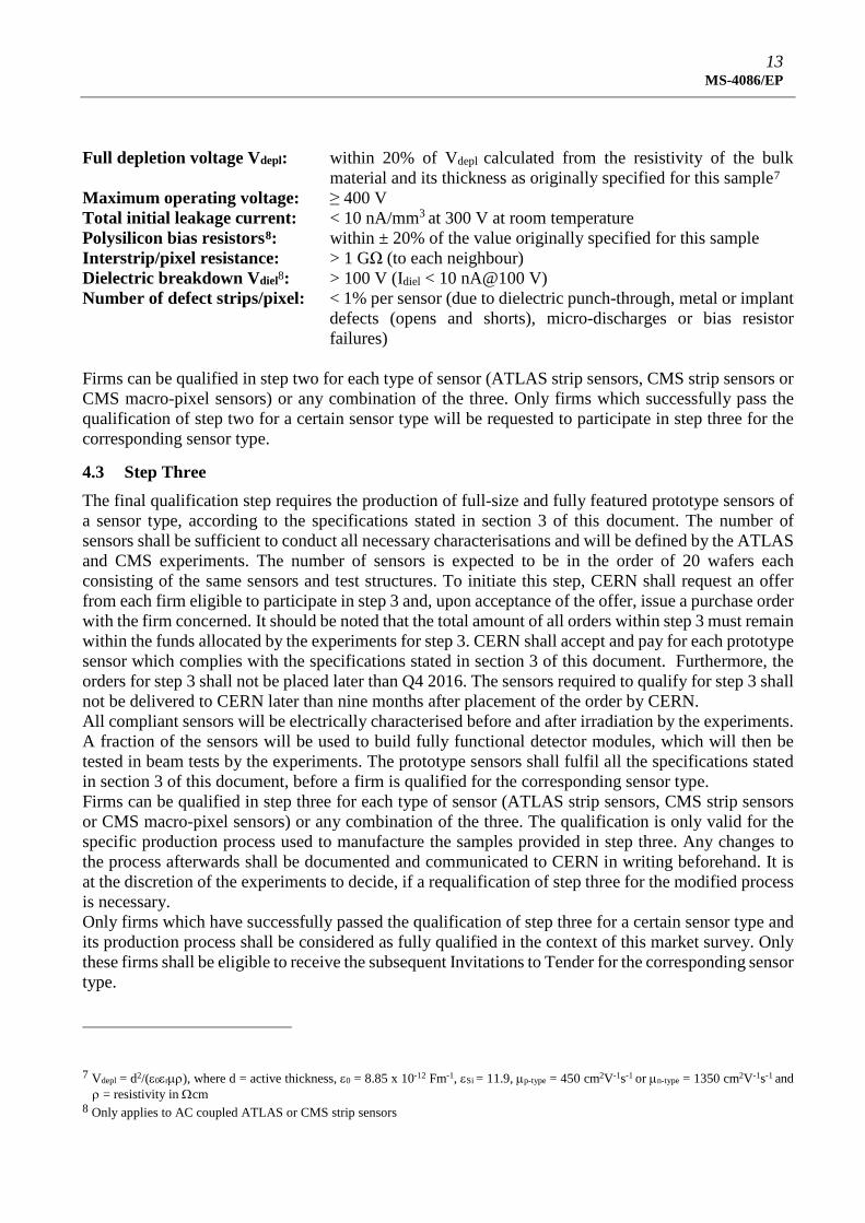
5.1 Provisional Delivery Schedule The contract is scheduled to be awarded in Q3/2017 for ATLAS strip sensors and in Q3/2018 for CMS strip and macro-pixel sensors following the Invitations to Tender which are planned to be issued in Q1/2017 and Q1/2018 respectively. The final delivery schedules will be stated in the Invitations to Tenders. The delivery of the sensors shall be structured into two phases: a pre-series production and a series production. The pre-series shall consist of about 5% of the contractual quantity, while the series production consists of the remaining 95% of the full contractual quantity. The start of the series production shall be contingent on completion of the pre-series according to the delivery schedule, and compliance of the pre-series sensors with the requirements of the final specifications, only some of which are covered in this Technical Description. CERN reserves the right to terminate the entire contract if the pre-series does not comply with these conditions without any compensation due to the contractor(s) for such termination. During the pre-series, the aim of the experiments is to test a large fraction of sensors and provide immediate feedback to the contractor(s). This should help in stabilising the production quality, but due to the increased demand on testing, the production throughput should be slowed down compared to the series production. A production time for the pre-series of 6 months is envisaged while the nominal duration of the series production is 2 to 3 years (Table 4). The delivery of sensors to CERN shall be made in a timely fashion after sensors are tested and diced by the contractor(s). Only sensors which comply with the technical specifications of the Invitations to Tender shall be sent to CERN including the test structures from the same wafers. The experiments will strive to qualify each batch received from the contractor(s) as soon as possible to provide timely feedback on the current quality of the production to the contractor(s). Deliveries shall be carried out at regular intervals according to the delivery schedule defined in the Invitations to Tender with a frequency which will presumably be either bi-weekly or monthly. The final delivery schedule for ATLAS and CMS sensors are independent of each other. The schedules of the CMS strip and macro-pixel sensors are envisaged to be synchronised. Furthermore, the delivery schedules shall be synchronised among the various contractors following contract splitting, in which case the delivery dates will presumably alternate between the contractors.
Key milestones ATLAS strip sensors CMS strip and macro-pixel sensors
Start of qualification step 1, requested response time April 2016, 4 weeks
Start of qualification step 2, requested response time May 2016, 4 weeks
Start of qualification step 3, fabrication duration June 2016, 9 months
Last order for qualification step 3 June 2016 March 2017 Invitations to Tender Q1 2017 Q1 2018 Contract award Q3 2017 Q3 2018 Pre-series production Q4 2017 – Q1 2018 Q4 2019 – Q1 2020 Start of series production Q2 2018 Q1 2021 Nominal contract duration 3 years 2-3 years Delivery intervals Monthly Bi-weekly or monthly
Table 4: Key milestones and preliminary dates for the issue of Invitations to Tender and award of contracts

15 MS-4086/EP
In the case of contract splitting, CERN reserves the right to take up a purchase option with a contractor in order to increase the production up to the full quantity of the supply of ATLAS strip sensors or CMS strip sensors or CMS macro-pixel sensors required if any of the other contractors fail to fulfil their obligations under their respective contracts. Under such circumstances, the original delivery schedule defined in the future Invitation to Tender shall be adapted to accommodate these changes.
5.2 Contract Follow-up and Progress Monitoring The contractor(s) shall assign a person responsible for the technical execution of the contract(s) and its follow-up, as well as a person responsible for the commercial follow-up, throughout the duration of the contract(s). They shall be able to communicate in English. The contractor(s) shall send a written progress report to CERN every six months until completion of the contract(s). All communications and documents shall be in English. This report shall include all the necessary information, in particular: • Actual progress in comparison to scheduled progress • Estimation of the delivery progress for the coming 6 months • Optimisations and changes implemented in production and testing

16 MS-4086/EP
6 CERN CONTACT PERSONS Persons to be contacted for technical matters concerning ATLAS:
Name/Department/Group Tel Email
Mr Yoshinobu Unno EP/UAT Tel: +81 29 864 5791 [email protected]
Mr Carlos Lacasta EP/UAT Tel: +34 96 354 3490 [email protected]
Mr Vitaliy Fadeyev EP/UAT Tel: +1 831 459 2126 [email protected] Persons to be contacted for technical matters concerning CMS:
Name/Department/Group Tel Email
Mr Marko Dragicevic EP/UCM Tel: +43 1 544 7328 36 [email protected]
Mr Alexander Dierlamm EP/UCM Tel: +49 721 608 23537 [email protected]
Mr Duccio Abbaneo EP/CMX Tel: +41 75 411 4074 [email protected] Persons to be contacted for commercial matters:
Name/Department/Group Tel Email
Mr Dante Gregorio IPT/PI-RC Tel: +41 22 767 76335 [email protected]
In case of absence: Mr Laszlo Abel IPT/PI-RC
Tel: +41 22 767 79561