master in electronic engineering
TRANSCRIPT

STUDY AND DESIGN OF RAIL-TO-RAIL OTAS IN 65 NM TECHNOLOGY
A Master's Thesis Submitted to the Faculty of the
Escola Tècnica d'Enginyeria de Telecomunicació de Barcelona
Universitat Politècnica de Catalunya by
Rafel Manera Escalero
In partial fulfilment of the requirements for the degree of
MASTER IN ELECTRONIC ENGINEERING
Advisor: Sergio Gomez Fernandez, Francesc Moll Echeto
Barcelona, October 2018


1
Title of the thesis: Study and Design of Rail-to-Rail OTAs in 65 nm Technology
Author: Rafel Manera Escalero
Advisor: Sergio Gomez Fernandez, Francesc Moll Echeto
Abstract
The Technological Unit of the Institute of Cosmos Science of the University of Barcelona (ICCUB-TECH) is focused on developing ultrafast read-out electronics for high-energy physics, medical imaging, astrophysics and space. The group has developed Application Specific Integrated Circuits (ASIC) for many different applications. In the framework of bridging developments and improvements in radiation detectors, ICCUB-TECH and the European Organization for Nuclear Research (CERN) collaborate in the design of a new front-end Application Specific Integrated Circuit (ASIC) (FastIC) in 65 nm CMOS technology, devoted for fast-timing applications in high energy physics, medical imaging, and other fields such as Fluorescence Lifetime Imaging, LIDAR and direct 3D-Imaging. This Master Thesis presents the design of three different Rail-to-Rail (RTR) Operational Transconductance Amplifiers (OTA) that will be included in the FastIC ASIC. The first version of the RTR OTA is a slow version with a GBW of 1,5 MHz and a power consumption of 70 µW, capable of driving a capacitive load of 1 pF. The second version of the RTR OTA is a fast version with a GBW of 115 MHz and a power consumption of around 700 µW, driving a capacitive load of 1 pF. The third version of the RTR OTA is a modification of the second version with a Slew Rate (SR) enhancement up to 330 V/µs and a GBW of 143 MHz.

2
Acknowledgements
I would like to thank all my colleagues from ICCUB-TECH for creating a pleasant work environment, which makes it a very good place to work. Special thanks to Sergio Gomez, for being the co-advisor of my Master Thesis and David Gascon for the guidance in analog design.
In addition, I would like to thank the people in the microelectronics group from CERN, specially Rafael Ballabriga and José Fernandez-Tenllado for welcoming me during my stay at CERN.
Finally, I would like to thank Francesc Moll for being the co-advisor of my Master Thesis.

3
Revision history and approval record
Revision Date Purpose
0 04/10/2018 Document creation
1 17/10/2018 Document revision
2 19/10/2018 Document approval
Written by: Reviewed and approved by:
Date 04/10/2018 Date 19/10/2018
Name Rafel Manera Escalero Name Francesc Moll Echeto
Position Project Author Position Project Supervisor

4
Table of contents
Abstract ............................................................................................................................ 1
Acknowledgements .......................................................................................................... 2
Revision history and approval record ................................................................................ 3
Table of contents .............................................................................................................. 4
List of Figures ................................................................................................................... 6
List of Tables .................................................................................................................... 7
1. Introduction ............................................................................................................... 8
1.1. ICCUB ................................................................................................................ 8
1.2. FastIC ................................................................................................................ 8
1.3. Objectives .......................................................................................................... 9
2. Rail-to-Rail Amplifiers .............................................................................................. 11
2.1. Why and when to use RTR amplifiers? ............................................................. 11
3. Rail-to-Rail OTA Architecture .................................................................................. 12
3.1. Input Stage ....................................................................................................... 12
3.2. Output Stage .................................................................................................... 15
3.3. Topology of the OTA ........................................................................................ 15
3.4. Small Signal Analysis ....................................................................................... 16
4. Slow RTR OTA ........................................................................................................ 19
4.1. Specification ..................................................................................................... 19
4.2. Simulations ....................................................................................................... 20
4.3. Sizing ............................................................................................................... 25
4.4. Layout .............................................................................................................. 26
5. Fast RTR OTA......................................................................................................... 27
5.1. Specification ..................................................................................................... 27
5.2. Simulations ....................................................................................................... 27
5.3. Sizing ............................................................................................................... 31
6. Fast RTR OTA with SR enhancement ..................................................................... 32
6.1. Specification ..................................................................................................... 32
6.2. Simulations ....................................................................................................... 35
6.3. Sizing ............................................................................................................... 38
7. Conclusions and Future Development ..................................................................... 39
Bibliography.................................................................................................................... 40
Appendix A. Signal integrity ............................................................................................ 41

5
Glossary ......................................................................................................................... 44

6
List of Figures
Figure 1. FastIC channel block diagram ......................................................................... 10
Figure 2. Commonly used amplifier configurations ......................................................... 11
Figure 3. Complete Rail-to-Rail OTA .............................................................................. 12
Figure 4. Rail-to-Rail input stage .................................................................................... 12
Figure 5. Input stage with gm equalization by three-times current mirrors ...................... 14
Figure 6. Input stage with gm equalization by Zener diode ............................................. 14
Figure 7. Class-AB output stage ..................................................................................... 15
Figure 8. Simplified small signal equivalent circuit .......................................................... 16
Figure 9. Test bench schematic ...................................................................................... 20
Figure 10. PMOS (green), NMOS (red) and total (blue) gm vs common-mode input voltage without gm equalization .................................................................................................. 22
Figure 11. PMOS (green), NMOS (red) and total (blue) gm vs common-mode input voltage with gm equalization ....................................................................................................... 23
Figure 12. GBW and Phase Margin vs common-mode input voltage .............................. 24
Figure 13. Slow RTR OTA layout .................................................................................... 26
Figure 14. PMOS (green), NMOS (red) and total (blue) gm vs common-mode input voltage without gm equalization .................................................................................................. 29
Figure 15. PMOS (green), NMOS (red) and total (blue) gm vs common-mode input voltage with gm equalization ....................................................................................................... 29
Figure 16. GBW and Phase Margin vs common-mode input voltage .............................. 30
Figure 17. Fast Rail-to-Rail OTA with SR enhancement schematic ................................ 33
Figure 18. SR enhancement circuit ................................................................................. 34
Figure 19. PMOS (green), NMOS (red) and total (blue) effective gm vs common-mode input voltage without gm equalization ...................................................................................... 36
Figure 20. PMOS (green), NMOS (red) and total (blue) effective gm vs common-mode input voltage with gm equalization ........................................................................................... 37
Figure 21. GBW and Phase Margin vs common-mode input voltage .............................. 37
Figure 22. Step signal (left) and first-order low-pass frequency response (right). ............ 41
Figure 23. Output signal ................................................................................................. 41

7
List of Tables
Table 1. Slow Rail-to-Rail OTA specification................................................................... 19
Table 2. Slow RTR OTA schematic simulation results .................................................... 21
Table 3. Slow RTR OTA Monte Carlo Process simulation results ................................... 21
Table 4. Slow RTR OTA Monte Carlo Mismatch simulation results ................................. 22
Table 5. Slow RTR OTA sizing ....................................................................................... 25
Table 6. Slow RTR OTA extracted layout simulation results ........................................... 26
Table 7. Fast RTR OTA specification.............................................................................. 27
Table 8. Fast RTR OTA schematic simulation results ..................................................... 27
Table 9. Fast RTR OTA Monte Carlo Process simulation results .................................... 28
Table 10. Fast RTR OTA Monte Carlo Mismatch simulation results ............................... 28
Table 11. Fast RTR OTA sizing ...................................................................................... 31
Table 12. Fast RTR OTA with SR enhancement specification ........................................ 32
Table 13. Fast RTR OTA with SR enhancement schematic simulation results ............... 35
Table 14. Fast RTR OTA with SR enhancement Monte Carlo Process simulation results ....................................................................................................................................... 35
Table 15. Fast RTR OTA Monte Carlo Mismatch simulation results ............................... 36
Table 16. Fast RTR OTA with SR enhancement sizing .................................................. 38

8
1. Introduction
1.1. ICCUB The Institute of Cosmos Sciences of the University of Barcelona (ICCUB) is an interdisciplinary center devoted to fundamental research in the fields of cosmology, astrophysics and particle physics. In addition, the institute has a strong technology program through its participation in international collaborations in observational astronomy and experimental particle physics.
The Technological Unit of the Institute of Cosmos Science of the University of Barcelona (ICCUB-TECH) is focused on developing ultrafast read-out electronics for high-energy physics, medical imaging, astrophysics and space. The group has developed Application Specific Integrated Circuits (ASIC) for many different applications.
• The LHCb detector is located at the European Organization for Nuclear Research (CERN) and dedicated to the research fields of CP violation, charm physics and rare decays of the B meson. An ASIC for the LHCb detector has been designed, produced and tested. It performs signal processing of Scintillator Pad Detector (SPD) multi-channel photo-multiplier tubes: amplification, shaping, and discrimination. More than 6000 channels are equipped.
• The LHCb will be upgraded in order to increase the instantaneous luminosity and new electronics will be required. More specifically, a new analog circuit has been designed for the Calorimeter sub-detector and for the scintillator fiber tracker (SciFi). The group developed 2 different ASICs in 130 and 350 nm technologies, for the calorimeter and tracking sub-detectors respectively.
• The Cherenkov Telescope Array (CTA) is intended to explore the Universe in depth in Very High Energy gamma rays and investigate cosmic non-thermal processes. Three different ASICs were designed for the CTA project, for pre-amplification, triggering and Signal Conditioning. Recently, a multipurpose Silicon Photomultiplier (SiPM) anode readout chip (referred as MUSIC) based on a novel low input impedance current conveyor has been developed. This chip allows using SiPMs instead of photomultiplier tubes (PMT) in CTA project, but it has also aroused the interest of CERN SHiP experiment, and neutron detector industry.
• Finally, two different ASICs have been developed for Positron Emission Tomography (PET). The first one is a readout circuit for SiPM arrays in a 350 nm technology, Flexible Time-over-Threshold (FlexToT). It includes a novel input stage and it offers an excellent timing measurement with good energy resolution measurement and pile-up detection. An upgraded version of this readout chip, High Resolution Flexible Time-over-Threshold (HRFlexToT), has been developed in a 180 nm technology. This ASIC provides state-of-the-art results in terms of Single Photon Time Resolution (SPTR) (60 ps RMS) [1] driving 3x3 mm2 SiPM, while allowing linear energy measurement.
1.2. FastIC This Master Thesis takes part in the CLUES project (reference FPA2016-80917-R) which goal is to advance the state of the art in detector technology to allow a breakthrough in molecular imaging, particularly in PET imaging. Several improvements in current PET

9
scanners are needed to transform in-vivo molecular imaging into a standard tool for personalized medicine: reduce the radiation dose, scan time and costs per patient. A way to achieve it is pushing Time-of-Flight (ToF) Coincidence Time Resolution (CTR) to ~10 ps [2], enabling direct 3D imaging.
Thus far, the NINO amplifier/discriminator [3], designed in 2004 at CERN, has been the reference ASIC in the ToF community, covering a wide range of applications but allowing only for time measurement and not energy measurement.
In the framework of bridging developments and improvements in radiation detectors, ICCUB and CERN collaborate in the design of a new front-end ASIC (FastIC) in 65 nm CMOS technology, devoted for fast-timing applications in high energy physics, medical imaging, and other fields such as Fluorescence Lifetime Imaging, LIDAR and direct 3D-Imaging.
From the need of being suitable for a wide range of applications, FastIC requires to be a highly configurable front-end, capable of coping with different detectors such as Photo Multiplier Tubes (PMTs), Micro Channel Plates (MCPs), and SiPMs, targeting a SPTR of 20 ps RMS for PMTs/MCPs and small SiPMs (for a detector charge ~100 fC). In contrast to the NINO ASIC, FastIC will be able to provide linearity in the energy measurement (2.5 % linearity error), as well as a fairly large dynamic range, from 5 uA to 20 mA peak, being capable of reading out photodetector signals in single-ended, with a configurable front-end for positive and negative polarities, and pseudo-differential modes and targeting a power consumption per channel around 5 mW [4].
1.3. Objectives The objective of this Master Thesis is to present the design of Rail-to-Rail (RTR) Operational Transconductance Amplifiers (OTA) that will be included in the FastIC ASIC. These amplifiers are implemented in TSMC 65 nm CMOS process. A block diagram of a channel of the ASIC is shown in Figure 1. These RTR OTAs are intended to be general purpose blocks to be used in different points of the ASIC. Three versions of the RTR OTA are designed with different specification.
• Slow RTR OTA • Fast RTR OTA • Fast RTR OTA with Slew Rate (SR) enhancement
The slow version features a GBW of 1 MHz and the two fast versions have a GBW of 100 MHz. The Slow RTR OTA version will be used in the Common Bias block (not shown in the block diagram) to propagate DC bias voltages. The Fast RTR OTA will be used in various blocks throughout the ASIC, some of these blocks are the Peak Detector and Track and Hold Hold (PDH) and the Ramp Generator, which is based in an integrator. The Fast RTR OTA with SR enhancement will be used to propagate the analog signal of the SiPM after the Shaper block to an output buffer.

10
Figure 1. FastIC channel block diagram
Since the work of this Master Thesis is inside the framework of a project in collaboration between ICCUB and CERN, the student has done a stay of three months at CERN, learning from the analog designers in the Experimental Physics, Electronic Systems for the Experiments, Micro Electronics (EP-ESE-ME) group at CERN.

11
2. Rail-to-Rail Amplifiers
RTR amplifiers are special amplifiers that admit input voltages from the negative supply voltage to the positive supply voltage. It is usual that amplifiers have the possibility of providing this range of voltages at their output. However, this is more complicated at the input [5].
2.1. Why and when to use RTR amplifiers? With the reduction in power supply voltages in new microelectronic technologies comes a reduction in the dynamic range of the circuits, so it is necessary to exploit the maximum of it. This is possible with RTR amplifiers since their input common-mode range (ICMR) is the maximum possible. However, although RTR output voltage swing will always be required, it will not be necessary at the input in all the cases. Three amplifier configurations are shown in Figure 2.
Figure 2. Commonly used amplifier configurations
Figure 2 a) shows an inverting amplifier, Figure 2 b) shows a non-inverting amplifier and Figure 2 c) shows a voltage follower. In inverting and non-inverting amplifiers, the output signal is divided by the open-loop gain so that the input hardly sees any signal. Thus, the voltage at the input will not reach RTR swings. On the other hand, in the voltage follower, the input has to be able to follow the output. In conclusion, the only configuration that needs a RTR ICMR is the voltage follower.

12
3. Rail-to-Rail OTA Architecture
The complete circuit schematic of the RTR OTA presented in this project [6] is shown in Figure 3. Different parts of the amplifier can be identified: input stage, summing circuit, class-AB control, bias block and output stage. These parts will be explained below.
Figure 3. Complete Rail-to-Rail OTA
3.1. Input Stage A special input stage is implemented in order to achieve a RTR ICMR. NMOS and a PMOS differential input pairs are connected in parallel, as shown in Figure 4. The NMOS input pair (M1 and M2) is active with input voltages between 𝑉"#$% + 𝑉'() and 𝑉"" while the PMOS input pair (M3 and M4) is active with input voltages between 𝑉(( and 𝑉"" − (𝑉"#$% +𝑉'(,).
Figure 4. Rail-to-Rail input stage

13
One drawback of the RTR input stage is that its transconductance 𝑔𝑚 varies by a factor of two over the ICMR, because in the middle section of this range, the two differential input pairs are working and the resulting 𝑔𝑚 is the sum of the transconductance of each pair. This variation of the 𝑔𝑚 impedes an optimal frequency compensation, because the gain-bandwidth product (GBW) of the amplifier is directly proportional to the transconductance of the input stage. The transconductance at the lower and upper section of the input range has to be multiplied by two to achieve a constant 𝑔𝑚 along the complete input range. Considering that input transistors operate in strong inversion, the 𝑔𝑚 is proportional to the square root of the drain current 𝐼".
𝑔𝑚%1% = 𝑔𝑚) + 𝑔𝑚,
𝑔𝑚) = 32𝜇)𝐶1789:9𝐼") ; 𝑔𝑚, = 32𝜇,𝐶17
8;:;𝐼",
Where 𝑔𝑚%1% is the resulting transconductance of the two differential pairs connected in parallel, 𝑔𝑚) and 𝑔𝑚, are the transconductances of the NMOS and PMOS pairs respectively. 𝜇) and 𝜇, are the mobility of the minority carriers for the NMOS and PMOS respectively, 𝐶17 is the capacitance of the oxide, 𝐼") and 𝐼", are the drain currents of the
NMOS and PMOS respectively and 89:9
and 8;:;
are the size ratios of the NMOS and PMOS
respectively.
For a transistor with a given dimensions, the mobility and the oxide capacitance will be constant, and it will be biased with a constant DC current. Thus, the following assumption can be made:
𝑔𝑚) ≈ 𝑔𝑚, ≈ 𝐶=𝐼>?$#
𝑔𝑚%1% = 𝐶A=𝐼") + =𝐼",B
If 𝐼") ≈ 𝐼",, to maintain 𝑔𝑚%1% constant, when one of the currents are zero, the other has to be multiplied by four:
√𝐴 + √𝐴 = √0 + √4𝐴 = 2√𝐴
A way to multiply the drain current by four is to add three times this drain current only when needed, in other words, when the other input pair is switched off. A circuit that performs this operation is shown in Figure 5 [5]. The transistors labelled as Mrn and Mrp are two current switches. When low common-mode input voltages are applied, the PMOS input pair operates and the NMOS pair is off, while the Mrp is conducting and Mrn is off. Mrp takes the current 𝐼G from the NMOS tail current source and directs it to the PMOS current mirror master and, since the current mirror has a gain of three, it adds three times the tail current to the existing PMOS tail current 𝐼G. Since the PMOS and NMOS tail currents are equal, the tail current of the PMOS equals 4𝐼G. If high common-mode input voltages are applied, the complementary situation happens.

14
Figure 5. Input stage with gm equalization by three-times current mirrors
Finally, if intermediate common-mode input voltages are applied, both switches Mrn and Mrp are off and the two input pairs are operating with a current 𝐼G.
This is not the only method to provide a constant 𝑔𝑚 throughout the ICMR. Another method is the use of Zener diodes [5], but since in CMOS technologies there are not Zener diodes, MOSFET transistors will be used.
Figure 6. Input stage with gm equalization by Zener diode
This technique is shown in Figure 6. For intermediate common-mode input voltages all the transistors are working. The tail current is now 8𝐼G and, since the diode-connected transistors are 6 times wider than the differential pair, they take 6 times the current flowing through each transistor of the differential pair, which is now 𝐼G.
The voltage across the two diode-connected transistors is 𝑉I which is two times 𝑉'(. Thus, when the voltage across the Zener diode is below 𝑉I, the transistors are off. When the input common-mode voltage increases, the PMOS input pair will turn off and the voltage across

15
the Zener diode will be below 𝑉I, turning the Zener diode off. With the Zener diode off, all the tail current has to flow through the NMOS input pair thus each transistor conducts 4𝐼G and its 𝑔𝑚 is increased by a factor of two.
3.2. Output Stage Class-AB biased output transistors connected in common-source configuration are chosen to achieve RTR voltage swing at the output node. The class-AB output stage is shown in Figure 7. It consists of two common-source connected transistors, O1 and O2, which are directly driven by two in-phase signal currents, 𝐼?)J and 𝐼?)K. Transistors M5 and M6 form the floating class-AB control, which gates are driven by the diode connected transistors M7-M8 and M9-10 respectively. The output transistors operate in class-AB because the voltage between their gates are maintained constant. If 𝐼?)J and 𝐼?)K are pushed into the output stage, the current of M5 will increase while the current of M6 will decrease by the same amount. Consequently, the voltage at the output transistors gates will increase, and the circuit will pull current from the output node. This continues until the current of M5 is equal to 𝐼GJ. The complementary behaviour happens when the input signals pull current from the output stage.
Figure 7. Class-AB output stage
3.3. Topology of the OTA In this section, the complete architecture of the rail-to-rail OTA will be explained. The complete schematic implemented is shown in Figure 3.
The conventional method to design a two-stage amplifier is to cascade those stages, however, this approach has a number of drawbacks. A few modifications to the cascade structure are made to obtain a compact OTA.
Input stage
Transistors P1a, P1b, N1a and N1b form the two complementary input differential pairs. P2 and N2 are the tail current sources that bias the differential pairs. The gate voltages for these current sources Vbp and Vbn are generated outside the OTA. P2a, P2b, N2a and
16
N2b are the three-times current mirrors which together with the switches PR and NR form the gm equalization circuit.
Summing circuit
Since the input stage described above has four output currents, an additional circuit is necessary to do the summation of these four currents. P3a, P3b, P4a, P4b, N3a, N3b, N4a and N4b form this summing circuit. It is based on a complementary folded cascode structure.
Floating class-AB control
P5 and N5 form the floating class-AB control explained above. It is shifted inside the summing circuit and is biased by the cascodes P4b and N4b. This way, the input transistors and the summing circuit mainly determine the noise and offset of the amplifier.
Bias block
The Bias circuit inside the OTA is formed by BP1, BP2, BP3, BP4, BP5, BN1, BN2, BN3, BN4 and BN5. The purpose of this block is to generate the bias voltages for the cascodes and the floating current sources. The necessary bias DC currents are generated and then copied to the corresponding transistors.
Class-AB output stage
O1 and O2 are the two output transistors. They are common-source configuration and biased in Class-AB. C1, C2 are frequency compensation capacitors, and R1 and R2 are zero-nulling resistors.
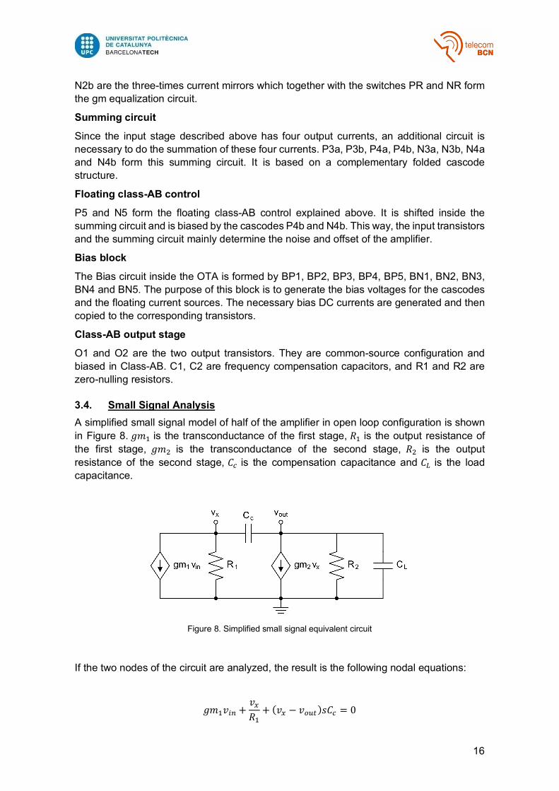
3.4. Small Signal Analysis A simplified small signal model of half of the amplifier in open loop configuration is shown in Figure 8. 𝑔𝑚J is the transconductance of the first stage, 𝑅J is the output resistance of the first stage, 𝑔𝑚K is the transconductance of the second stage, 𝑅K is the output resistance of the second stage, 𝐶M is the compensation capacitance and 𝐶: is the load capacitance.
Figure 8. Simplified small signal equivalent circuit
If the two nodes of the circuit are analyzed, the result is the following nodal equations:
𝑔𝑚J𝑣?) +𝑣7𝑅J+ (𝑣7 − 𝑣1O%)𝑠𝐶M = 0

17
𝑔𝑚K𝑣7 +𝑣1O%𝑅K
+ 𝑠𝐶:𝑣1O% + (𝑣1O% − 𝑣7)𝑠𝐶M = 0
Solving the system of equations form by the two equations above:
𝑣1O%(𝑠)𝑣?)(𝑠)
=𝑔𝑚J𝑅J𝑅K(𝑔𝑚K − 𝑠𝐶M)
𝐶M𝐶:𝑅J𝑅K𝑠K + A𝐶:𝑅K + 𝐶M(𝑅J + 𝑅K + 𝑔𝑚K𝑅J𝑅K)B𝑠 + 1 (1)
To easily identify the dominant, non-dominant pole and the zero of the system, the transfer function has to be written in the form:
𝑣1O%𝑣?)
=𝐴R: S1 +
𝑠𝑧JU
S1 + 𝑠𝑝JUS1 + 𝑠
𝑝KU (2)
If the denominator in (2) is expanded, the following expression is obtained:
W1 +𝑠𝑝JXW1 +
𝑠𝑝KX = 1 +
𝑠𝑝J+𝑠𝑝K+
𝑠K
𝑝J𝑝K
Since the dominant pole is designed to be far from the non-dominant pole with the goal of good stability (𝑝J ≪ 𝑝K), the following simplification can be made:
𝑣1O%𝑣?)
=𝐴R: S1 +
𝑠𝑧JU
1 + 𝑠𝑝J+ 𝑠K𝑝J𝑝K
(3)
Now, the terms of (1) can be identified in (3), and solving for 𝑠 = 0 the open-loop gain of the OTA is obtained:
𝐴R: = 𝐴J𝐴K = 𝑔𝑚J𝑔𝑚K𝑅1O%J𝑅1O%K
If the denominator of (1) is equalled to 0 and the resulting equation is solved for 𝑠, the zero of the OTA is obtained:
𝑔𝑚K − 𝑠𝐶M = 0

18
𝑧J =𝑔𝑚K
𝐶M
In the denominator, the term that multiply 𝑠 can be identified to solve the dominant pole:
𝐶:𝑅K + 𝐶M(𝑅J + 𝑅K + 𝑔𝑚K𝑅J𝑅K) =1𝑝J
𝑝J =1
𝐶M𝑅J + 𝐶M𝑅K + 𝐶:𝑅K + 𝐶M𝑔𝑚K𝑅J𝑅K≈
1𝐶M𝑔𝑚K𝑅J𝑅K
From the term multiplying 𝑠K the non-dominant pole can be calculated:
𝐶M𝐶:𝑅J𝑅K =1
𝑝J𝑝K
𝑝K =1
𝐶M𝐶:𝑅J𝑅K𝑝J=𝑔𝑚K
𝐶:
Finally, the GBW of the amplifier can be calculated multiplying the open-loop gain of the amplifier by its bandwidth. Since the dominant pole is the one which limits the bandwidth of the amplifier, the GBW can be obtained as:
𝐺𝐵𝑊 = 𝐴R:𝑝J =𝑔𝑚J
𝐶M
With the equations presented above, the effect of the different elements of the circuit to the different parameters can be observed.

19
4. Slow RTR OTA
The first OTA designed is a slow version with a GBW of 1 MHz. This OTA will be used to propagate DC bias voltages.
4.1. Specification The specifications wanted for this OTA are listed in Table 1. Low offset and low power consumption are requirements for the usage of this OTA.
Table 1. Slow Rail-to-Rail OTA specification
Parameter Value
GBW 1 MHz
Phase Margin 60º
Gain 70 dB
Random Offset 1 mV
PSRR at 10 Hz 70 dB
Power consumption 100 µW
In this version of the RTR OTA, the differential input pair transistors are in weak inversion. The relation between gm and ID is not the same as in strong inversion. In weak inversion, the transconductance is directly proportional to the drain current of the transistor, as shown in expression (4). This means that to double the transconductance of the transistor, the current has to increase by a factor two and not by a factor four. Thus, the current mirror ratio has to be 1:1 instead of 1:3.
𝑔𝑚]? =𝐼"𝑛𝑉%
(4)
Where 𝑔𝑚]? is the transconductance of a MOSFET transistor in weak inversion, 𝐼" is its drain current, 𝑉% is the thermal voltage and 𝑛 is a factor that depends on the bias current of the transistor.

20
4.2. Simulations
Figure 9. Test bench schematic
The test bench used to simulate the RTR OTA is shown in Figure 9. The supply voltage (i.e. between VDD and VSS) is 1,2 V. An ideal current source and two diode connected transistors are used to generate the bias voltages Vbn and Vbp. This bias current will be generated in the common bias block from a Bandgap Reference inside the ASIC. The voltage source vin generate the DC common-mode input voltage, the AC voltage for AC analysis and an square signal to test the Slew Rate of the amplifier. The voltage source vpsrr generated an AC voltage to test the Power Supply Rejection Ratio (PSRR) of the amplifier. The component “iprobe” is used to test the stability parameters, which is equivalent to a short circuit in DC and an open circuit in AC. The load applied to the amplifier is a capacitor which value is CL = 1 pF.
This version of the RTR OTA is implemented with the schematic shown in Figure 3. The results of the nominal simulation of the schematic are shown in Table 2. The goal of this version of the RTR OTA is to obtain good stability and a small random offset, in order to obtain reliability to propagate DC voltages.

21
Table 2. Slow RTR OTA schematic simulation results
Parameter Value
GBW 1,534 MHz
Phase Margin 72,03º
Gain 92,88 dB
PSRR at 10 Hz 82,7 dB
Power consumption 70,33 µW
RMS Noise 277,1 µV
Slew Rate (rise) 708,7 V/ms
Monte Carlo simulations are performed to see the changes that process variations can make on the performance of the Slow RTR OTA. The results are shown in Table 3. The differences due to process variations are relatively small.
Table 3. Slow RTR OTA Monte Carlo Process simulation results
Parameter Mean Std Deviation
GBW 1,54 MHz 72,72 kHz
Phase Margin 72,07º 2,685º
Gain 92,81 dB 0,6745 dB
PSRR at 10 Hz 82,44 dB 8,506 dB
Power consumption 70,69 µW 5,935 µW
RMS Noise 277,1 µV 6,195 µV
Slew Rate (rise) 708,5 V/ms 35,95 V/ms
Monte Carlo Mismatch simulations are performed to evaluate the random offset of the amplifier. The results are shown in Table 4. The standard deviation of the offset is below 1 mV throughout the complete ICMR.

22
Table 4. Slow RTR OTA Monte Carlo Mismatch simulation results
Parameter Mean Std Deviation
Offset @ 0,2 V 5,289 µV 803,7 µV
Offset @ 0,4 V -456,2 nV 814,4 µV
Offset @ 0,6 V -2,723 µV 796,5 µV
Offset @ 0,8 V 42,23 µV 945,9 µV
Offset @ 1 V 39,92 µV 955 µV
Corner simulations are also performed, taking into account the following cases:
• Power supply voltage: 1,1 V, 1,2 V and 1,3 V • Temperature: -40ºC and 80ºC • Process corners: TT, FF, SS, FS and SF
The worst cases are listed:
• At 80ºC in the TT corner the Phase Margin decreases to 65º • At 80ºC in the FF corner the PSRR decreases to 49 dB
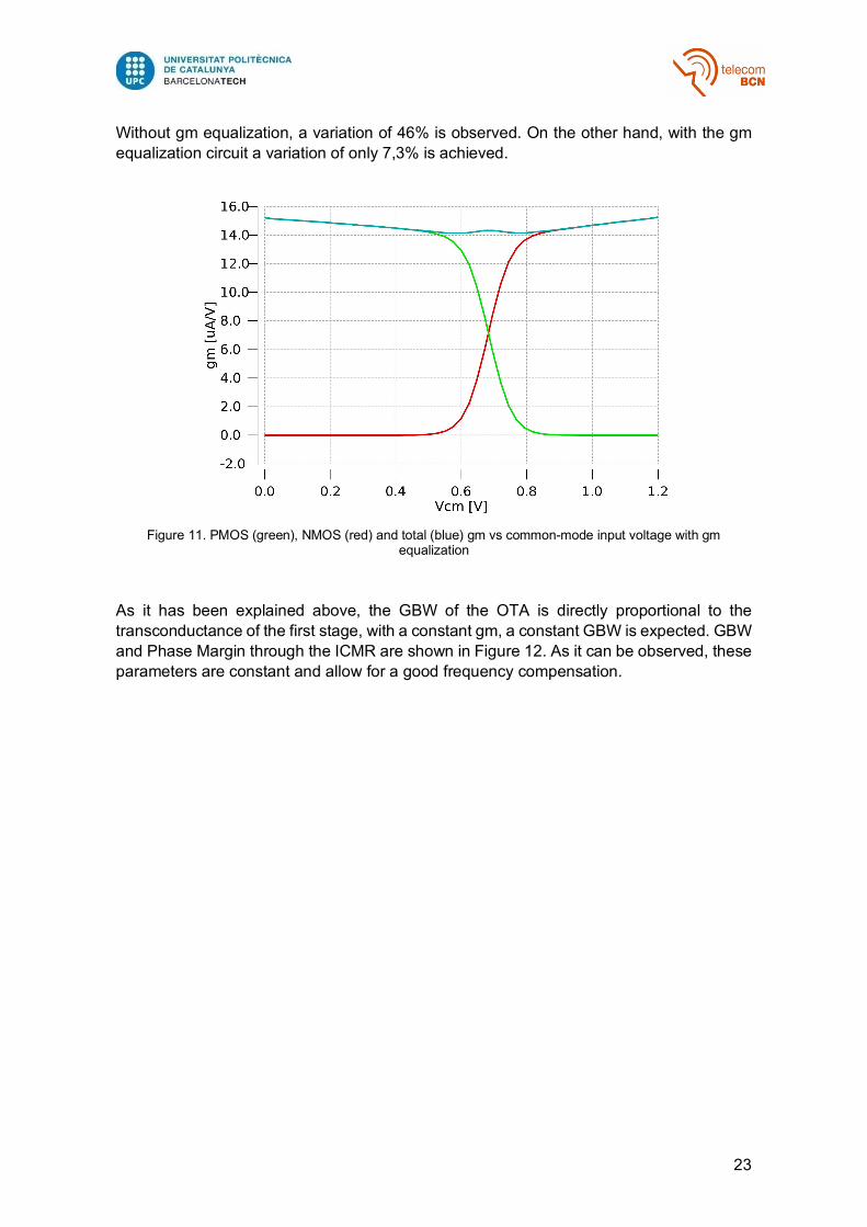
In Figure 10 the transconductance of the differential input pair in function of the common-mode input voltage without the gm equalization circuit is shown, and in Figure 11, the same is shown but with the gm equalization circuit to illustrate the effect of the gm equalization circuit described above in this version of the RTR OTA.
Figure 10. PMOS (green), NMOS (red) and total (blue) gm vs common-mode input voltage without gm
equalization
23
Without gm equalization, a variation of 46% is observed. On the other hand, with the gm equalization circuit a variation of only 7,3% is achieved.
Figure 11. PMOS (green), NMOS (red) and total (blue) gm vs common-mode input voltage with gm
equalization
As it has been explained above, the GBW of the OTA is directly proportional to the transconductance of the first stage, with a constant gm, a constant GBW is expected. GBW and Phase Margin through the ICMR are shown in Figure 12. As it can be observed, these parameters are constant and allow for a good frequency compensation.

24
Figure 12. GBW and Phase Margin vs common-mode input voltage

25
4.3. Sizing The sizes of the different components of the Slow RTR OTA are listed in Table 5.
Table 5. Slow RTR OTA sizing
Component Size (M x W/L µm)
P1a, P1b, PR 8 x 5/1
N1a, N1b, NR 8 x 5/1
P2, P2a, P2b, BP1, BP2 2 x 5/2
N2, N2a, N2b, BN1, BN2 2 x 5/2
P3a, P3b, BP3 4 x 7,5/6
N3a, N3b, BN3 8 x 3,5/10
P4a, P4b, BP4 1 x 5/2
N4a, N4b, BN4 1 x 5/2
P5, P6, BP5 8 x 7,5/0,13
N5, N6, BN5 8 x 7,5/0,13
C1, C2 715 fF
R1, R2 36 kΩ
O1 24 x 5/0,13
O2 8 x 5/0,13

26
4.4. Layout
The layout of the Slow RTR OTA is shown in Figure 13 and the results of nominal simulation1 are shown in Table 6. The extraction of parasitic components is made with Calibre tool. Some parameters are significantly worse than in the schematic simulation. The Gain of the amplifier has decreased around 10 dB but it still fits the specification. In addition, PSRR at low frequency has decreased more than 15 dB.
Figure 13. Slow RTR OTA layout
Table 6. Slow RTR OTA extracted layout simulation results
Parameter Value
GBW 1,447 MHz
Phase Margin 70,59º
Gain 81,96 dB
PSRR at 10 Hz 64,3 dB
Power consumption 69,82 µW
RMS Noise 251,2 µV
Slew Rate (rise) 671,2 V/ms
1 Only nominal simulations are performed with the layout extraction due to a series of software issues with the extraction of parasitic components

27
5. Fast RTR OTA
The second OTA designed is a fast version with a GBW of 100 MHz. This OTA will be used to propagate DC bias voltages when a fast response is needed.
5.1. Specification The specification wanted for this OTA are listed in Table 7. The offset and the power consumption is higher than the slow version due to the increase in speed.
Table 7. Fast RTR OTA specification
Parameter Value
GBW 100 MHz
Phase Margin 60º
Gain 60 dB
Random Offset 5 mV
PSRR at 10 Hz 60 dB
Power consumption 800 µW
5.2. Simulations The simulations are performed with the test bench schematic shown in Figure 9.
Table 8. Fast RTR OTA schematic simulation results
Parameter Value
GBW 115,3 MHz
Phase Margin 70,94º
Gain 76,06 dB
PSRR at 10 Hz 56,66 dB
Power consumption 725,7 µW
RMS Noise 306,6 µV
Slew Rate (rise) 52,9 V/µs

28
This version of the RTR OTA is implemented with the schematic shown in Figure 3. The results of the nominal simulation of the schematic are shown in Table 8.
Monte Carlo simulations are performed to see the changes that process variations can make on the performance of the Fast RTR OTA. The results are shown in Table 9. The differences due to process variations are relatively small.
Table 9. Fast RTR OTA Monte Carlo Process simulation results
Parameter Mean Std Deviation
GBW 115,7 MHz 5,718 MHz
Phase Margin 70,86º 1,561º
Gain 76 dB 0,2746 dB
PSRR at 10 Hz 56,82 dB 0,9873 dB
Power consumption 724,7 µW 39,82 µW
RMS Noise 306,7 µV 5,487 µV
Slew Rate (rise) 53,11 V/µs 2,174 V/µs
Monte Carlo Mismatch simulations are performed to evaluate the random offset of the amplifier. The results are shown in Table 10. The standard deviation of the offset is below 5 mV throughout the complete ICMR.
Table 10. Fast RTR OTA Monte Carlo Mismatch simulation results
Parameter Mean Std Deviation
Offset @ 0,2 V 261,9 µV 2,758 mV
Offset @ 0,4 V 208,5 µV 2,81 mV
Offset @ 0,6 V 256 µV 2,717 mV
Offset @ 0,8 V 378,3 µV 3,14 mV
Offset @ 1 V 362,4 µV 3,086 mV
Corner simulations are also performed, taking into account the following cases:
• Power supply voltage: 1,1 V, 1,2 V and 1,3 V. • Temperature: -40ºC and 80ºC. • Process corners: TT, FF, SS, FS and SF.
29
The worst cases are listed:
• At -40ºC in the SS corner with a power supply voltage of 1,1 V the Phase Margin decreases to 55º.
• At 80ºC in the FF corner with a power supply voltage of 1,1 V the PSRR decreases to 47 dB.
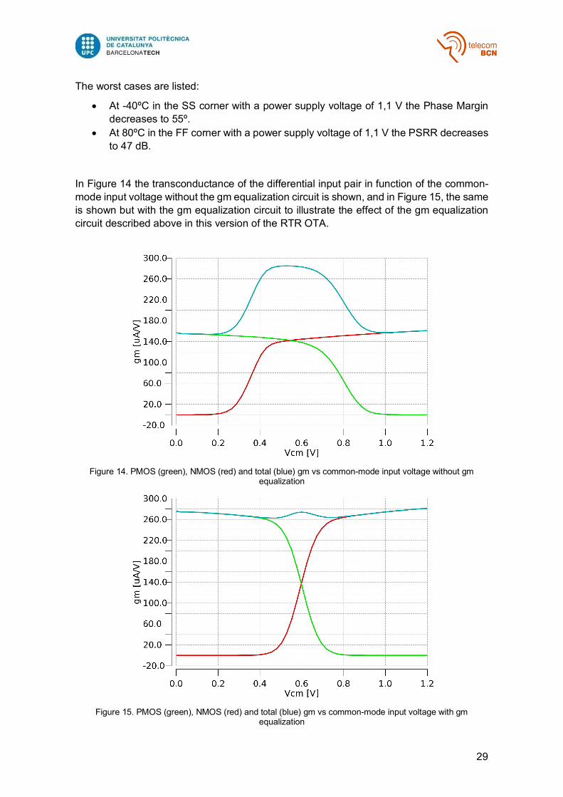
In Figure 14 the transconductance of the differential input pair in function of the common-mode input voltage without the gm equalization circuit is shown, and in Figure 15, the same is shown but with the gm equalization circuit to illustrate the effect of the gm equalization circuit described above in this version of the RTR OTA.
Figure 14. PMOS (green), NMOS (red) and total (blue) gm vs common-mode input voltage without gm
equalization
Figure 15. PMOS (green), NMOS (red) and total (blue) gm vs common-mode input voltage with gm
equalization

30
Without gm equalization, a variation of 46% is observed. On the other hand, with the gm equalization circuit a variation of only 6,5% is achieved.
GBW and Phase Margin through the ICMR are shown in Figure 16.
Figure 16. GBW and Phase Margin vs common-mode input voltage

31
5.3. Sizing The sizes of the different components of the Fast RTR OTA are listed in Table 11.
Table 11. Fast RTR OTA sizing
Component Size (M x W/L µm)
P1a, P1b, PR 8 x 5/0,3
N1a, N1b, NR 8 x 5/0,3
P2, P2a, P2b, BP1, BP2 4 x 5/1
N2, N2a, N2b, BN1, BN2 4 x 5/1
P3a, P3b, BP3 2 x 5/0,3
N3a, N3b, BN3 4 x 7,5/1
P4a, P4b, BP4 1 x 5/0,13
N4a, N4b, BN4 1 x 5/0,13
P5, P6, BP5 8 x 7,5/0,13
N5, N6, BN5 4 x 5/0,13
C1, C2 160 fF
R1, R2 3 kΩ
O1 30 x 5/0,13
O2 10 x 5/0,13

32
6. Fast RTR OTA with SR enhancement
The third version of OTA is a modification of the previous version (Fast RTR OTA). This version will be used to drive the signal of a SiPM sensor, which is a fast signal with a high slope. Thus, an amplifier to drive this signal needs a high SR, but maintaining the GBW.
The reason to increase the SR without increasing the GBW is to be able to drive signals with a bandwidth similar to the GBW of the amplifier but with a rise time of a few nanoseconds, but attenuating higher frequency harmonics or high frequency noise.
6.1. Specification The specification wanted for this OTA are listed in Table 12. In this case, the SR specification substitute the Random Offset specification. With the techniques applied to increase the SR of the amplifier, the random offset of the amplifier becomes worse.
In Appendix A, the expression (14) defines the minimum SR that the amplifier needs to maintain signal integrity. Since a RTR OTA is designed to be used in a voltage follower configuration, the BW can be considered equal to the GBW, and if a step from VSS to VDD is considered, for this particular amplifier, the minimum SR can be expressed as:
𝑆𝑅 >𝑉""𝐺𝐵𝑊0,35
=1,2 · 100 · 10e
0,35= 342,9𝑉/𝜇𝑠
Table 12. Fast RTR OTA with SR enhancement specification
Parameter Value
GBW 100 MHz
Phase Margin 60º
Gain 60 dB
Slew Rate 300 V/µs
PSRR at 10 Hz 40 dB
Power consumption 1,6 mW
This version of the RTR OTA is implemented with the schematic shown in Figure 17. Three different techniques are applied to increase the SR of the amplifier.

33
Figure 17. Fast Rail-to-Rail OTA with SR enhancement schematic
Input differential pair shrinking
In the other two versions of the RTR OTA, the differential input pair transistors have a large W/L ratio to maintain them in weak inversion, improving the gm/ID ratio and reducing the offset due to mismatch. In this version of the RTR OTA, the width of the differential input pair transistors has been reduced compared to the Fast RTR OTA version, moving the transistors out of weak inversion and thus degrading the gm/ID ratio
Source degeneration
This technique consists of connecting resistors between the sources of the differential input pair transistors and the tail current sources. This changes the effective transconductance of the transistor, which now is [6]:
𝑔𝑚h( =𝑔𝑚
1 + 𝑔𝑚𝑅𝑆
Where 𝑔𝑚h( is the effective transconductance of the transistor with a source degeneration resistor, 𝑔𝑚 is the original transconductance of the transistor and 𝑅𝑆 is the value of the source degeneration resistor.
This new effective transconductance is reduced with respect to the original one, but it does not affect the current flowing through the transistor thus achieving the same effect than reducing the W/L ratio, which is reduce the gm/ID ratio.
Indirect frequency compensation
With direct frequency compensation, the zero calculated above is a right-hand plane (RHP) zero due to the feed-forward component of the compensation current. This RHP zero
34
decreases the phase margin thus the compensation capacitance has to be large. The RHP zero can be eliminated by blocking the feed-forward component of the compensation current using, for example, the common-gate amplifier that forms the cascode transistors of the folded cascode structure of the RTR OTA [8]. This technique improves the phase margin of the amplifier allowing the reduction of the compensation capacitance. Since the main contribution to the limitation in SR is this compensation capacitance, the SR of the RTR OTA increases.
Other techniques
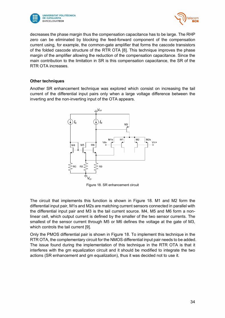
Another SR enhancement technique was explored which consist on increasing the tail current of the differential input pairs only when a large voltage difference between the inverting and the non-inverting input of the OTA appears.
Figure 18. SR enhancement circuit
The circuit that implements this function is shown in Figure 18. M1 and M2 form the differential input pair, M1s and M2s are matching current sensors connected in parallel with the differential input pair and M3 is the tail current source. M4, M5 and M6 form a non-linear cell, which output current is defined by the smaller of the two sensor currents. The smallest of the sensor current through M5 or M6 defines the voltage at the gate of M3, which controls the tail current [9].
Only the PMOS differential pair is shown in Figure 18. To implement this technique in the RTR OTA, the complementary circuit for the NMOS differential input pair needs to be added. The issue found during the implementation of this technique in the RTR OTA is that it interferes with the gm equalization circuit and it should be modified to integrate the two actions (SR enhancement and gm equalization), thus it was decided not to use it.
35
6.2. Simulations The simulations are performed with the test bench schematic shown in Figure 9.
Table 13. Fast RTR OTA with SR enhancement schematic simulation results
Parameter Value
GBW 143,4 MHz
Phase Margin 70,39º
Gain 59,88 dB
PSRR at 10 Hz 44,19 dB
Power consumption 1,582 µW
RMS Noise 877,4 µV
Slew Rate (rise) 335,9 V/µs
Monte Carlo simulations are performed to see the changes that process variations can make on the performance of the Fast RTR OTA. The results are shown in Table 14. The differences due to process variations are relatively small.
Table 14. Fast RTR OTA with SR enhancement Monte Carlo Process simulation results
Parameter Mean Std Deviation
GBW 143,7 MHz 6,996 MHz
Phase Margin 70,22º 2,147º
Gain 59,86 dB 0,5328 dB
PSRR at 10 Hz 44,44 dB 0,4258 dB
Power consumption 1,578 mW 0,1466 mW
RMS Noise 878,5 µV 19,05 µV
Slew Rate (rise) 341,8 V/µs 33,34 V/µs
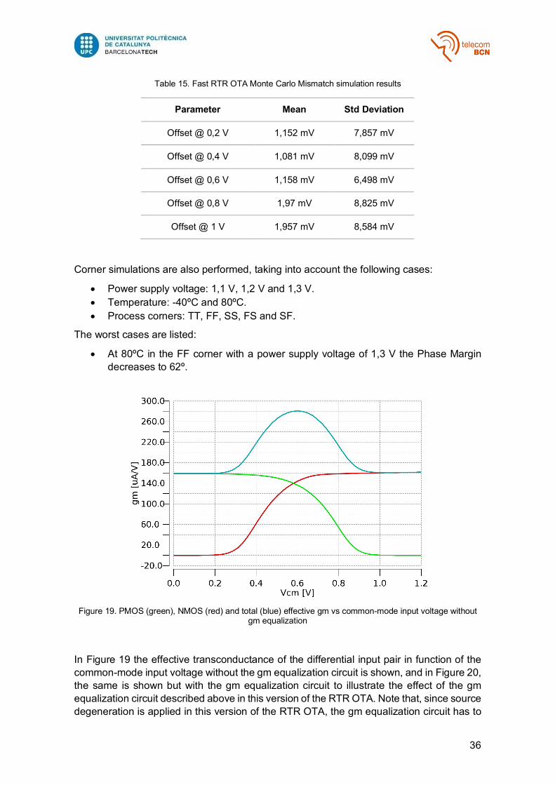
Monte Carlo Mismatch simulations are performed to evaluate the random offset of the amplifier. The results are shown in Table 15. The random offset is higher than in the Fast RTR OTA due to the techniques implemented to improve the SR. This is an important parameter to take into account when deciding where to use this OTA.
36
Table 15. Fast RTR OTA Monte Carlo Mismatch simulation results
Parameter Mean Std Deviation
Offset @ 0,2 V 1,152 mV 7,857 mV
Offset @ 0,4 V 1,081 mV 8,099 mV
Offset @ 0,6 V 1,158 mV 6,498 mV
Offset @ 0,8 V 1,97 mV 8,825 mV
Offset @ 1 V 1,957 mV 8,584 mV
Corner simulations are also performed, taking into account the following cases:
• Power supply voltage: 1,1 V, 1,2 V and 1,3 V. • Temperature: -40ºC and 80ºC. • Process corners: TT, FF, SS, FS and SF.
The worst cases are listed:
• At 80ºC in the FF corner with a power supply voltage of 1,3 V the Phase Margin decreases to 62º.
Figure 19. PMOS (green), NMOS (red) and total (blue) effective gm vs common-mode input voltage without
gm equalization
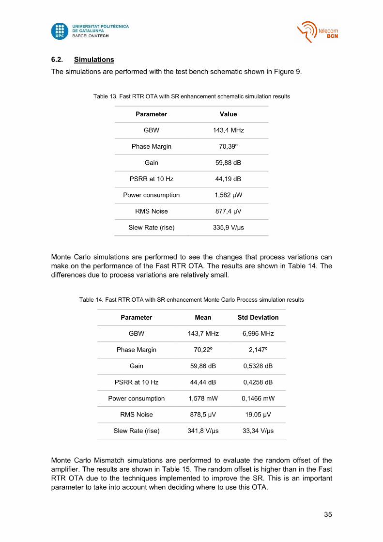
In Figure 19 the effective transconductance of the differential input pair in function of the common-mode input voltage without the gm equalization circuit is shown, and in Figure 20, the same is shown but with the gm equalization circuit to illustrate the effect of the gm equalization circuit described above in this version of the RTR OTA. Note that, since source degeneration is applied in this version of the RTR OTA, the gm equalization circuit has to

37
be tuned to obtain the lower error in the effective transconductance of the differential input pair.
Without gm equalization, a variation of 43% is observed. On the other hand, with the gm equalization circuit a variation of only 15% is achieved.
Figure 20. PMOS (green), NMOS (red) and total (blue) effective gm vs common-mode input voltage with gm
equalization
Figure 21. GBW and Phase Margin vs common-mode input voltage

38
GBW and Phase Margin through the ICMR are shown in Figure 21.
6.3. Sizing The sizes of the different components of the Fast RTR OTA with SR enhancement are listed in Table 16.
Table 16. Fast RTR OTA with SR enhancement sizing
Component Size (M x W/L µm)
P1a, P1b, PR 6 x 5/0,3
N1a, N1b, NR 3 x 5/0,3
RS1a, RS1b, RS2a, RS2b 4 kΩ
P2, P2a, P2b, BP1, BP2 6 x 5/1
N2, N2a, N2b, BN1, BN2 6 x 5/1
P3a, P3b, BP3 4 x 5/0,3
N3a, N3b, BN3 8 x 7,5/1
P4a, P4b, BP4 1 x 5/0,13
N4a, N4b, BN4 1 x 5/0,13
P5, P6, BP5 8 x 7,5/0,13
N5, N6, BN5 4 x 5/0,13
C1, C2 83 fF
R1, R2 8 kΩ
O1 30 x 5/0,13
O2 10 x 5/0,13

39
7. Conclusions and Future Development
In this Master Thesis, three different RTR OTAs have been designed to be used in the FastIC ASIC. The first version of the RTR OTA is a slow version with a GBW of 1,5 MHz and a power consumption of 70 µW, capable of driving a capacitive load of 1 pF. Layout of this version has been done.
The second version of the RTR OTA is a fast version with a GBW of 115 MHz and a power consumption of around 700 µW, driving a capacitive load of 1 pF. The third version of the RTR OTA is a modification of the second version with SR enhancement, with a GBW of 143 MHz and increasing the SR to 330 V/µs.
As a future work, firstly, the layout of the two Fast RTR OTAs, will be finished. When the layout of the amplifiers is finished and optimized, one of the following steps is to design higher-level blocks that include this OTAs. The PDH is a block that the student will be working on.
The Fast RTR OTA with SR enhancement is an amplifier that can be improved. The integration between SR enhancement circuits and the gm equalization circuit has to be studied. Also, the random offset of the amplifier is high, thus techniques to reduce it will be explored.
In addition, new layout techniques will be explored to improve the performance of the amplifiers.
Since the student will continue working at ICCUB, this work might become the starting point of a PhD thesis.

40
Bibliography
[1] D. Gascon, J.M. Fernández-Tenllado, R. Ballabriga, S. Gomez. “Review of SiPM readout circuitry.” ICASiPM 2018.
[2] P. Lecoq. “Pushing the limits in Time-Of-Flight PET imaging.” IEEE Transactions on Radiation and Plasma Medical Sciences 1.6 (2017): pp. 473-485. DOI: 10.1109/TRPMS.2017.2756674.
[3] F. Anghinolfi, P. Jarron, F. Krummenacher, E. Usenko, M. C. S. Williams. “NINO, an ultra-fast, low-power, front-end amplifier discriminator for the Time-Of-Flight detector in ALICE experiment.” Nuclear Science Symposium Conference Record, 2003 IEEE. Vol. 1. IEEE, 2003. DOI: 10.1109/NSSMIC.2003.1352067.
[4] J.M. Fernández-Tenllado, D. Gascon, R. Ballabriga, S. Gomez. “Development of a highly configurable ASIC for Fast Timing applications.” 4th FAST WG3/4/5 Meeting (Ljubljana) (2018).
[5] Sansen, Willy MC. “Analog Design Essentials”. Spriger, Nertherland, 2006.
[6] R. Hogervorst, J. P. Tero, R. G. Eschauzier, J. H. Huijsing. “A compact power-efficient 3 V CMOS rail-to-rail input/output operational amplifier for VLSI cell libraries.” IEEE journal of solid-state circuits 29.12 (1994): pp. 1505-1513. DOI: 10.1109/4.340424.
[7] R. Jacob, Baker. “CMOS: circuit design, layout, and simulation”. Vol. 1. John Wiley & Sons, 2008.
[8] Vadim V. Ivanov, Igor M. Filanovsky. “Operational amplifier speed and accuracy improvement: analog circuit design with structural methodology.” Vol. 763. Springer Science & Business Media, 2006.
[9] Howard W. Johnson, Martin Graham. “High-speed digital design: a handbook of black magic.” Vol. 1. Upper Saddle River, NJ: Prentice Hall, 1993.
[11] V. Sriskaran. “Design of Rad-Hard Analog Blocks for the Medipix4 Project.” M.S. thesis, CERN, 2016.
41
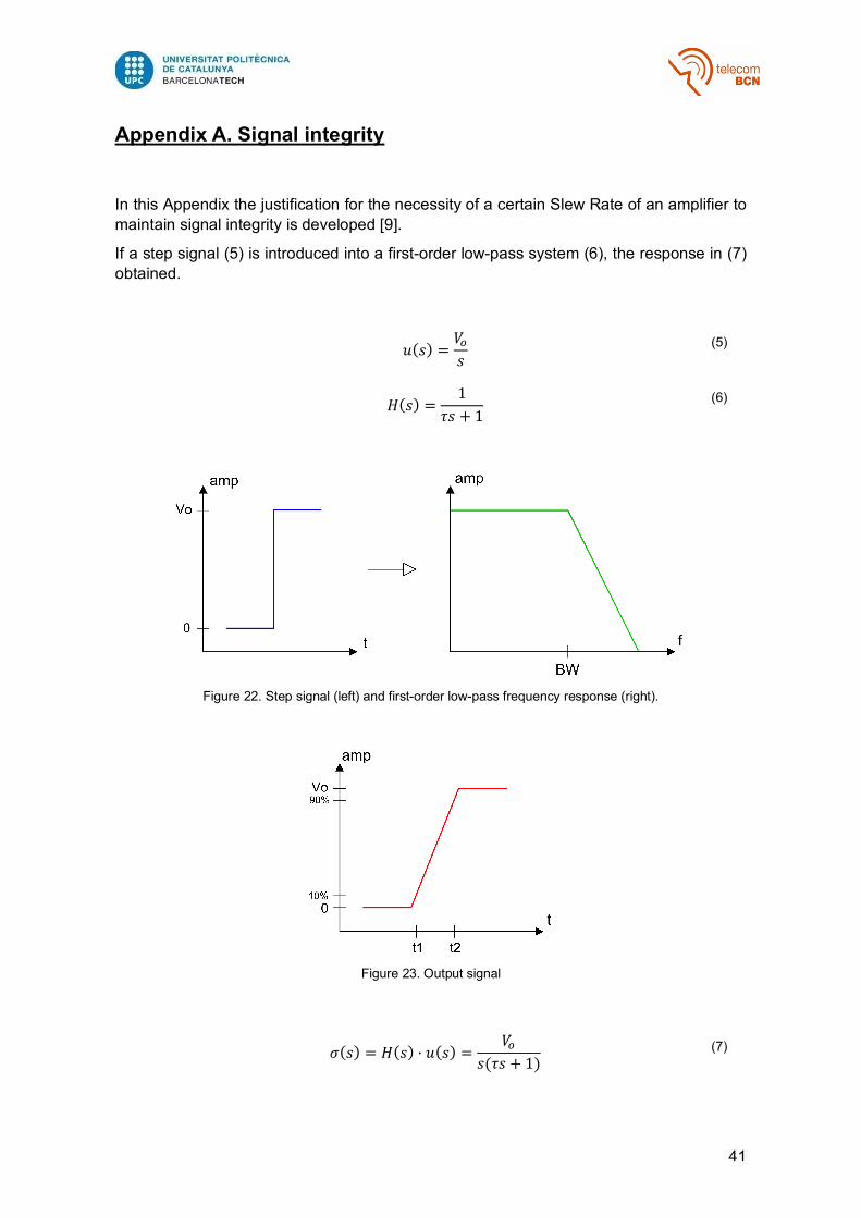
Appendix A. Signal integrity
In this Appendix the justification for the necessity of a certain Slew Rate of an amplifier to maintain signal integrity is developed [9].
If a step signal (5) is introduced into a first-order low-pass system (6), the response in (7) obtained.
𝑢(𝑠) =𝑉1𝑠
(5)
𝐻(𝑠) =1
𝜏𝑠 + 1 (6)
Figure 22. Step signal (left) and first-order low-pass frequency response (right).
Figure 23. Output signal
𝜎(𝑠) = 𝐻(𝑠) · 𝑢(𝑠) =𝑉1
𝑠(𝜏𝑠 + 1) (7)

42
If the inverse Laplace transform is applied to (7), the response in temporal domain in (8) is obtained.
𝜎(𝑡) = 𝑉1 S1 − 𝑒o% pq U (8)
Isolating the variable time in (8) the time for a given amplitude can be calculated.
𝑡 = −𝜏 ln t1 −
𝜎(𝑡)𝑉1
u (9)
The instants for 10% and 90% of the amplitude can be calculated as:
𝑡J(10%) = −𝜏 ln(1 − 0,1) = −𝜏 ln(0,9)
𝑡K(90%) = −𝜏 ln(1 − 0,9) = −𝜏 ln(0,1)
The difference between these two instants can be defined as the rise time of the signal.
𝑡w = 𝑡K − 𝑡J = −𝜏 ln(0,1) + 𝜏 ln(0,9) = 𝜏(ln(0,9) − ln(0,1)) ≈ 2,1972𝜏 (10)
In a first-order low-pass system, the time constant is
𝜏 =1
2𝜋𝐵𝑊 (11)
Replacing (11) in (10)
𝑡w =
2,19722𝜋𝐵𝑊
≈0,35𝐵𝑊
(12)
The Slew Rate is defined as the ratio between the voltage of the step and its rise time
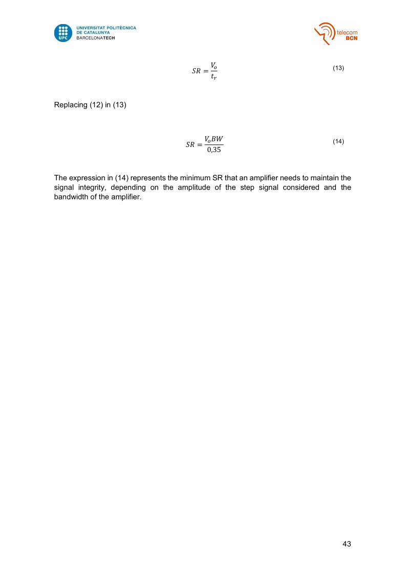
43
𝑆𝑅 =𝑉1𝑡w
(13)
Replacing (12) in (13)
𝑆𝑅 =𝑉1𝐵𝑊0,35
(14)
The expression in (14) represents the minimum SR that an amplifier needs to maintain the signal integrity, depending on the amplitude of the step signal considered and the bandwidth of the amplifier.

44
Glossary
ICCUB Institute of Cosmos Sciences of the University of Barcelona
ASIC Application Specific Integrated Circuit
CERN European Organization for Nuclear Research
SPD Scintillator Pad Detector
CTA Cherenkov Telescope Array
SiPM Silicon Photomultiplier
PMT Photomultiplier Tube
PET Positron Emission Tomography
ToT Time over Threshold
SPTR Single Photon Time Resolution
ToF Time of Flight
CTR Coincidence Time Resolution
MCP Microchannel Plate
RTR Rail to Rail
OTA Operational Transconductance Amplifier
RMS Root Mean Square
GBW Gain Bandwidth Product
PDH Peak Detector and Hold
ICMR Input Common Mode Range
PSRR Power Supply Rejection Ratio
BW Bandwidth
RHP Right Hand Plane