materialnews newsletter2018 final · polymer semiconductor film and a gold substrate (fig.1a). in...
TRANSCRIPT
NEWSM a t e r i a l s S c i e n c e & E n g i n e e r i n gU n i v e r s i t y o f C a l i f o r n i a , S a n D i e g o
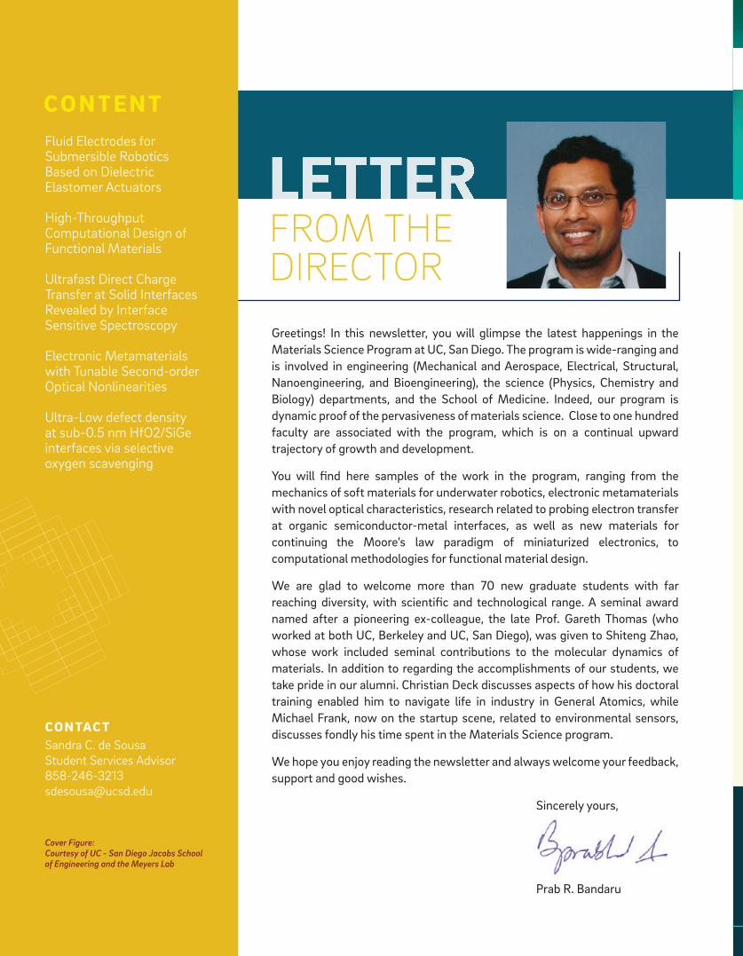
FROM THEDIRECTORGreetings! In this newsletter, you will glimpse the latest happenings in the Materials Science Program at UC, San Diego. The program is wide-ranging and is involved in engineering (Mechanical and Aerospace, Electrical, Structural, Nanoengineering, and Bioengineering), the science (Physics, Chemistry and Biology) departments, and the School of Medicine. Indeed, our program is dynamic proof of the pervasiveness of materials science. Close to one hundred faculty are associated with the program, which is on a continual upward trajectory of growth and development.
You will find here samples of the work in the program, ranging from the mechanics of soft materials for underwater robotics, electronic metamaterials with novel optical characteristics, research related to probing electron transfer at organic semiconductor-metal interfaces, as well as new materials for continuing the Moore’s law paradigm of miniaturized electronics, to computational methodologies for functional material design.
We are glad to welcome more than 70 new graduate students with far reaching diversity, with scientific and technological range. A seminal award named after a pioneering ex-colleague, the late Prof. Gareth Thomas (who worked at both UC, Berkeley and UC, San Diego), was given to Shiteng Zhao, whose work included seminal contributions to the molecular dynamics of materials. In addition to regarding the accomplishments of our students, we take pride in our alumni. Christian Deck discusses aspects of how his doctoral training enabled him to navigate life in industry in General Atomics, while Michael Frank, now on the startup scene, related to environmental sensors, discusses fondly his time spent in the Materials Science program.
We hope you enjoy reading the newsletter and always welcome your feedback, support and good wishes.
Sincerely yours,
Prab R. Bandaru
C O N T E N T
C O N TA C T
Cover Figure: Courtesy of UC - San Diego Jacobs Schoolof Engineering and the Meyers Lab
Fluid Electrodes for Submersible Robotics Based on Dielectric Elastomer Actuators
High-Throughput Computational Design of Functional Materials
Ultrafast Direct Charge Transfer at Solid Interfaces Revealed by Interface Sensitive Spectroscopy
Electronic Metamaterials with Tunable Second-order Optical Nonlinearities
Ultra-Low defect density at sub-0.5 nm HfO2/SiGe interfaces via selective oxygen scavenging
Sandra C. de SousaStudent Services [email protected]

Recently, dielectric elastomer actuators (DEAs) have gathered interest for soft robotics due to their low cost, light weight, large strain, low power consumption, and high energy density. However, developing reliable, compliant electrodes for DEAs remains an ongoing challenge due to issues with fabrication, uniformity of the conductive layer, and mechanical sti�ening of the actuators caused by conductive materials with large Young’s moduli. In this work, we present a method for preparing, patterning, and utilizing conductive fluid electrodes. When we submerse the DEAs in a bath containing a fluid connected to ground, the bath serves as a second electrode, obviating the need for depositing a conductive layer to serve as either of the electrodes required of most DEAs. When we apply a positive electrical potential to the fluid in the actuator with respect to ground, the electric field across the dielectric membrane induces an electrostatic force on the membrane, which compresses the membrane and causes the actuator to bend (Fig. 1).
In this work, we demonstrated a bimorph DEA actuator comprised of VHB dielectric layers and water for compliant electrodes. Since water serves as the conductive layer, we overcome buoyancy issues that may be a challenge for alternative approaches such as sealed electromechanical systems or pneumatically powered fluidic elastomer actuators. The actuator consists of a simple saline solution serving as the compliant electrodes and non-prestretched acrylic adhesive for the dielectric layers, minimizing the cost and complexity of these bimorph actuators, while also reducing the sensitivity of the electrodes to mechanical abrasion that is problematic for many other electrode materials for DEAs. By alternating the side of the tri-layer actuator to which we applied an electrical field, we achieved bi-directional motion that enables propulsion through the surrounding fluid at up to 9.2 mm/s (Fig. 2). This research provides an initial look into the implementation of fluid electrode actuators for submersible soft robotics and aims to open the door to low-power underwater robots towards search and rescue and environmental monitoring applications.
Before joining the mechanical engineering faculty at the Jacobs School of Engineering at UC San Diego, Tolley was a postdoctoral fellow at Harvard University’s Wyss Institute for Biologically Inspired Engineering, working in the Harvard Microbotics Laboratory from 2011 to fall 2014. He earned his Ph.D. and master’s in the Creative Machines Lab (formerly Computational Synthesis Lab) at Cornell University. He has a bachelor’s degree from McGill University in Montreal.
1Fluid Electrodes For Submersible RoboticsBased On Dielectric Elastomer Actuators
Fig. 1. Design and working principle of bimorph DEA with fluid electrodes in a bath of a grounded, conductive fluid. Top: A bimorph DE actuator comprises three layers of acrylic tape and two fluid chambers. Bottom: A voltage applied between one of the chambers and the external bath causes opposite charges to attract, compressing the barrier dielectric layer in thickness and expanding it in area. The unactuated chamber constrains the expansion of the activated layer, causing the bimorph to curl away from the activated side.
Fig. 2. Images from video of bimorph actuator swimming from left to right with time indicated. Nominal electric field was 20 MV/m. Maximum speed was 9.2 mm/s.
PROF. M. TOLLEY

All-oxide electronics represent one of the most promising technologies for next-generation nanoelectronic devices beyond traditional silicon technology, and producing two-dimensional electron gas (2DEG) at the interface of heterostructures is one of the most attractive technologies for nanoelectronics application. One example is the recent discovery of 2DEG at the interface between LaAlO₃ and SrTiO₃ perovskite insulators. In our recent work, we show that we are able to realize a rapid design of SrTiO₃-based 2DEG systems from perovskite oxide quantum database using high-throughput first-principles quantum mechanics calculations. The high-throughput design is enabled by introducing a group of combinatorial descriptors that characterize the polar character, lattice mismatch, band gap, and the band alignment between the perovskite-oxide-based band insulators and the SrTiO₃. Equipped with these combinatorial descriptors, we have carried out a high-throughput screening of all the polar perovskite compounds, uncovering 42 compounds of potential interests (Figure 1). Of these, Al-, Ga-, Sc-, and Ta-based compounds can form a 2DEG with SrTiO₃, while In-based compounds exhibit a strain-induced strong polarization when depositedon SrTiO₃ substrate. Our approach,by defining materials descriptors solely based on the bulk materials properties, and by relying on the perovskite -oriented quantum materials repository, opens new avenues for the discovery of perovskite-oxide-based functional interface materials in a high-throughput fashion. By using the similar strategy, current and future work by Yang group is to carry out high-throughput design of other types of functional materials for optoelectronics, such as hybrid perovskite based functional materials for solar cells and light-emitting applications.
2
High-Throughput ComputationalDesign of Functional Materials
Figure 1 Flowchart of high-throughput screening of candidate perovskite oxides for forming 2DEG based on polar/nonpolar heterostructures. The number of candidate perovskite oxides after each step’s screening, i.e., entries for the next-step screening, is given. Scientific Reports, 6, 34667 (2016), doi:10.1038/srep34667
Professor Yang’s research focuses on the first-principles (ab-initio) design of functional materials with various applications from the nanoelectronics to the energy conversion. At UC San Diego, Yang’s recent research has focused on the first-principles design of perovskite-based interface materials, including the design of perovskite-based two-dimensional electron gas systems and interfacial magnetism, high-throughput design of hybrid perovskites for optoelectronics, and sulfide-based two-dimensional materials for hydrodesulfrization applications, and the development of software framework for high-throughput materials design.
ABO3/SrTiO3
PROF. K. YANG
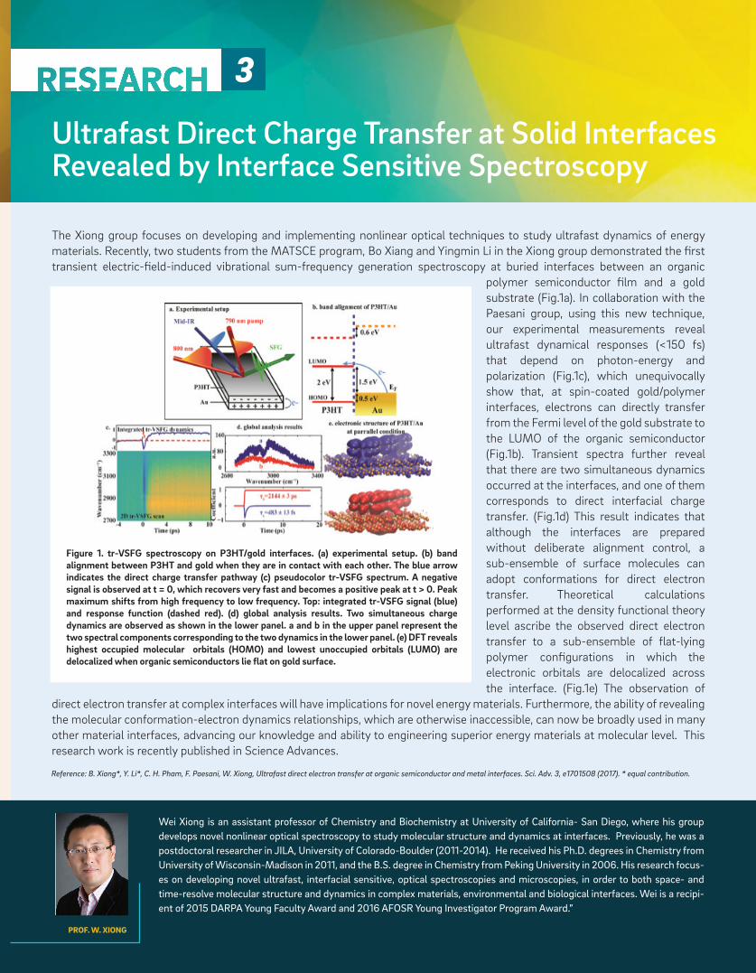
The Xiong group focuses on developing and implementing nonlinear optical techniques to study ultrafast dynamics of energy materials. Recently, two students from the MATSCE program, Bo Xiang and Yingmin Li in the Xiong group demonstrated the first transient electric-field-induced vibrational sum-frequency generation spectroscopy at buried interfaces between an organic
polymer semiconductor film and a gold substrate (Fig.1a). In collaboration with the Paesani group, using this new technique, our experimental measurements reveal ultrafast dynamical responses (<150 fs) that depend on photon-energy and polarization (Fig.1c), which unequivocally show that, at spin-coated gold/polymer interfaces, electrons can directly transfer from the Fermi level of the gold substrate to the LUMO of the organic semiconductor (Fig.1b). Transient spectra further reveal that there are two simultaneous dynamics occurred at the interfaces, and one of them corresponds to direct interfacial charge transfer. (Fig.1d) This result indicates that although the interfaces are prepared without deliberate alignment control, a sub-ensemble of surface molecules can adopt conformations for direct electron transfer. Theoretical calculations performed at the density functional theory level ascribe the observed direct electron transfer to a sub-ensemble of flat-lying polymer configurations in which the electronic orbitals are delocalized across the interface. (Fig.1e) The observation of
direct electron transfer at complex interfaces will have implications for novel energy materials. Furthermore, the ability of revealing the molecular conformation-electron dynamics relationships, which are otherwise inaccessible, can now be broadly used in many other material interfaces, advancing our knowledge and ability to engineering superior energy materials at molecular level. This research work is recently published in Science Advances.
3
Figure 1. tr-VSFG spectroscopy on P3HT/gold interfaces. (a) experimental setup. (b) band alignment between P3HT and gold when they are in contact with each other. The blue arrow indicates the direct charge transfer pathway (c) pseudocolor tr-VSFG spectrum. A negative signal is observed at t = 0, which recovers very fast and becomes a positive peak at t > 0. Peak maximum shifts from high frequency to low frequency. Top: integrated tr-VSFG signal (blue) and response function (dashed red). (d) global analysis results. Two simultaneous charge dynamics are observed as shown in the lower panel. a and b in the upper panel represent the two spectral components corresponding to the two dynamics in the lower panel. (e) DFT reveals highest occupied molecular orbitals (HOMO) and lowest unoccupied orbitals (LUMO) are delocalized when organic semiconductors lie flat on gold surface.
Reference: B. Xiang*, Y. Li*, C. H. Pham, F. Paesani, W. Xiong, Ultrafast direct electron transfer at organic semiconductor and metal interfaces. Sci. Adv. 3, e1701508 (2017). * equal contribution.
Wei Xiong is an assistant professor of Chemistry and Biochemistry at University of California- San Diego, where his group develops novel nonlinear optical spectroscopy to study molecular structure and dynamics at interfaces. Previously, he was a postdoctoral researcher in JILA, University of Colorado-Boulder (2011-2014). He received his Ph.D. degrees in Chemistry from University of Wisconsin-Madison in 2011, and the B.S. degree in Chemistry from Peking University in 2006. His research focus-es on developing novel ultrafast, interfacial sensitive, optical spectroscopies and microscopies, in order to both space- and time-resolve molecular structure and dynamics in complex materials, environmental and biological interfaces. Wei is a recipi-ent of 2015 DARPA Young Faculty Award and 2016 AFOSR Young Investigator Program Award.”
Ultrafast Direct Charge Transfer at Solid InterfacesRevealed by Interface Sensitive Spectroscopy
PROF. W. XIONG

4
Electronic Metamaterials with TunableSecond-order Optical Nonlinearities
Article by, Hung-Hsi Lin, PhD, a recent UC San Diego graduate, who conducted research under his advisor, Dr. Yeshaiahu Fainman. Professor Fainman joined the faculty at UCSD in July 1990 following a faculty appointment at the University of Michigan. Current research interests in his group include the investigation of artificial dielectric properties of nanostructures; polarization selective computer-generated holograms and their applications for image processing, transparent photonic switching fabric and networks, and packaging optoelectronic devices and systems; programmable di�ractive optical elements; 3-D holographic optical storage; di�ractive optics with multifunctionality; optical information processing with femtosecond laser pulses; nonconventional 3-D imaging and displays; quantum cryptography for photonic network security and privacy.
The ability to engineer metamaterials with tunable nonlinear optical properties is crucial for nonlinear optics. Traditionally, metals have been employed to enhance nonlinear optical interactions through field localization. Here, inspired by the electronic properties of materials, we introduce and demonstrate experimentally an asymmetric metal-semiconductor-metal (MSM) metamaterial that exhibits a large and electronically tunable e�ective second-order optical susceptibility (χ(2)), as shown in figure 1.
The induced χ(2) originates from the interaction between the third-order optical susceptibility of the semiconductor (χ(3)) with the engineered internal electric field resulting from the two di�erent metals (i.e., Aluminum and Nickel) possessing dissimilar work function at its interfaces with amorphous silicon (a-Si). We perform the free-space second-harmonic generation (SHG) experiments and demonstrate a five times larger SHG intensity from the MSM metamaterial, compared to contributions from its constituents.
In addition to their passive optical behavior, MSM metamaterials also enable the active control of their second-order nonlinear optical response by applying an external electric field using the constituent metals as electrodes, as shown in figure 2(a). The nonlinear response of MSMs in figure 2(b), is proportional to the di�erence in the work functions of the cladding metals, shown to be actively controlled by external electric field resulting in tunable e�ective Xzzz(2) tensor component ranging from 2.8 to 15.6 pm/V, making it suitable for on-chip optical switching and modulation.
Further enhancement in the e�ective χ(2) of the MSM metamaterials can be achieved by using a semiconductor
possessing a larger χ(3), with a larger breakdown voltage, and/or by improving the quality of a-Si fabrication process to increase its breakdown voltage. Moreover, the material stacks are grown using magnetron sputter machine in one-step process without the need of breaking vacuum at room temperature, making this MSM metamaterial suitable for CMOS-compatible all-optical spatial signal processing devices with tailored space invariant as well as space variant nonlinear spatial impulse response.
Figure 1. Schematic and SEM image of a 5nm Ni/25nm a-Si/ 5nm Al MSM
Figure 2. (a) Schematic of an active MSM metamaterial. (b) Measured SHG intensity under variant DC voltage (dots), and the red fitting curve showing the quadratic dependency.
PROF. Y. FAINMAN
5
Ultra-Low defect density at sub-0.5 nm HfO2/SiGeinterfaces via selective oxygen scavenging
Article by, Mahmut S. Kavrik, a 5th year PhD student, working with Dr. Andy Kummel. Kummel’s lab investigates the chemistry of microelectronics processing using both room temperature (RT) and low temperature (LT) scanning tunneling microscopy (STM) and spectroscopy (STS), molecular beams, laser spectroscopy, impedance spectroscopy and density functional theory (DFT) calculations. Professor Kummel also runs Cancer Researchers in Nanotechnology, a cross-training translational research program whose goal is to recruit and train young scientists to bring the tools of emerging technologies in nanoscience, nanoengineering, mesoscale engineering, and imaging sciences to the care of cancer patients.
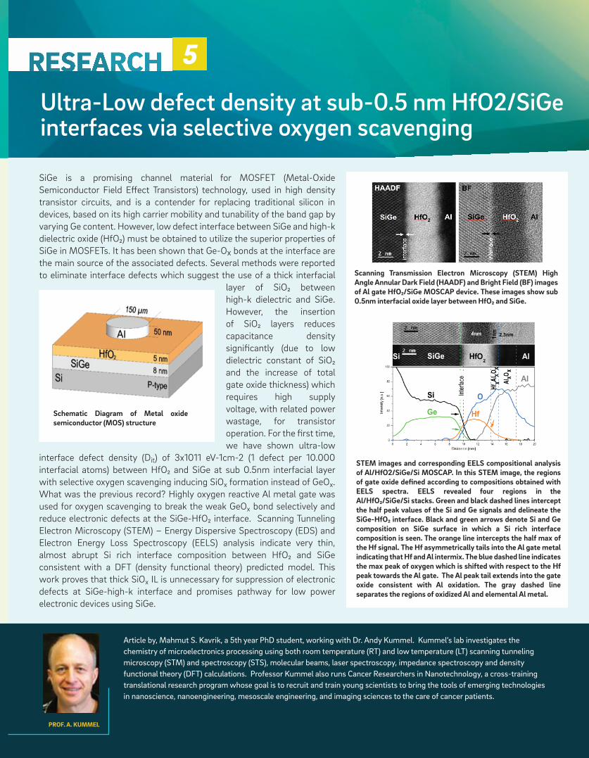
Scanning Transmission Electron Microscopy (STEM) High Angle Annular Dark Field (HAADF) and Bright Field (BF) images of Al gate HfO₂/SiGe MOSCAP device. These images show sub 0.5nm interfacial oxide layer between HfO₂ and SiGe.
STEM images and corresponding EELS compositional analysis of Al/HfO2/SiGe/Si MOSCAP. In this STEM image, the regions of gate oxide defined according to compositions obtained with EELS spectra. EELS revealed four regions in the Al/HfO₂/SiGe/Si stacks. Green and black dashed lines intercept the half peak values of the Si and Ge signals and delineate the SiGe-HfO₂ interface. Black and green arrows denote Si and Ge composition on SiGe surface in which a Si rich interface composition is seen. The orange line intercepts the half max of the Hf signal. The Hf asymmetrically tails into the Al gate metal indicating that Hf and Al intermix. The blue dashed line indicates the max peak of oxygen which is shifted with respect to the Hf peak towards the Al gate. The Al peak tail extends into the gate oxide consistent with Al oxidation. The gray dashed line separates the regions of oxidized Al and elemental Al metal.
SiGe is a promising channel material for MOSFET (Metal-Oxide Semiconductor Field E�ect Transistors) technology, used in high density transistor circuits, and is a contender for replacing traditional silicon in devices, based on its high carrier mobility and tunability of the band gap by varying Ge content. However, low defect interface between SiGe and high-k dielectric oxide (HfO₂) must be obtained to utilize the superior properties of SiGe in MOSFETs. It has been shown that Ge-Ox bonds at the interface are the main source of the associated defects. Several methods were reported to eliminate interface defects which suggest the use of a thick interfacial
layer of SiO₂ between high-k dielectric and SiGe. However, the insertionof SiO₂ layers reduces capacitance density significantly (due to low dielectric constant of SiO₂ and the increase of total gate oxide thickness) which requires high supply voltage, with related power wastage, for transistor operation. For the first time, we have shown ultra-low
interface defect density (Dit) of 3x10¹¹ eV-1cm-2 (1 defect per 10.000 interfacial atoms) between HfO₂ and SiGe at sub 0.5nm interfacial layer with selective oxygen scavenging inducing SiOx formation instead of GeOx. What was the previous record? Highly oxygen reactive Al metal gate was used for oxygen scavenging to break the weak GeOx bond selectively and reduce electronic defects at the SiGe-HfO₂ interface. Scanning Tunneling Electron Microscopy (STEM) – Energy Dispersive Spectroscopy (EDS) and Electron Energy Loss Spectroscopy (EELS) analysis indicate very thin, almost abrupt Si rich interface composition between HfO₂ and SiGe consistent with a DFT (density functional theory) predicted model. This work proves that thick SiOx IL is unnecessary for suppression of electronic defects at SiGe-high-k interface and promises pathway for low power electronic devices using SiGe.
Schematic Diagram of Metal oxide semiconductor (MOS) structure
PROF. A. KUMMEL
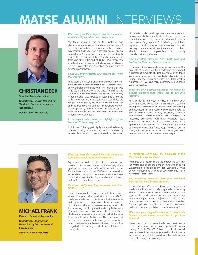
What was your thesis topic? How did the related work impact your future career trajectory?
My thesis research was on the synthesis and characterization of carbon nanotubes. In my current job, I develop advanced new materials – ceramic composites, fuels, etc., particularly for nuclear energy applications. Although my work now is not directly related to carbon nanotube research, many of the tools and skills I learned at UCSD have been very beneficial to me in my current job, where I still have a big focus on controlling fabrication and processing to optimize performance.
Could you briefly describe your career path - from UCSD to now?
I had spent the last year and a half or so while I was in graduate school working part time at General Atomics, so my transition to industry was very quick; that was in 2009, and I have been there since. When I started we had a very small group, and my work was very hands-on, and I was involved in setting up a new lab with fabrication and characterization capabilities. As the group has grown, my role is now less hands-on and I do a lot more management. I coordinate work on bigger projects, which involve multiple areas of research both in my lab and with university and national lab collaborators.
In retrospect, what were the highlights of the Materials Science program?
I think one of the biggest highlights was the diversity of research being performed. Just within the lab of my advisor, Prof. Vecchio, there was work on bone and
CHRISTIAN DECK
MICHAEL FRANK Research Scientist, AerNos, Inc.
Dissertation: Applications Bioinspired by Sea Urchins and Spongy Bone
Advisor: Joanna McKittrick
Scientist, General Atomics
Dissertation: Carbon Nanotubes: Synthesis, Characterization, and Applications
Advisor: Prof. Ken Vecchio
biomaterials, bulk metallic glasses, metal-intermetallic laminates, and other materials in addition to the carbon nanotube research I did. I also had collaborations with Prof. Bandaru’s group and Prof. Talke’s group. I think exposure to a wide range of research was very helpful, not only to learn about di�erent materials but to think about di�erent approaches to solving materials-related problems.
Any interesting memories from (both good and bad!) of the Materials Science program?
I represented the Materials Science program on the graduate student council for a while, and we arranged a number of graduate student events. A lot of these were co-sponsored with graduate students from Scripps, and those were particularly fun. I also went to a number of TMS and MRS conferences, and those were memorable.
What are your suggestions/advice for Materials Science students who would like to get into industry?
First, be flexible and open-minded. It is unlikely your work in industry will exactly match what you worked on in graduate school, so think about how your training and education can be applied to solve new problems. Second, communication is very important, especially non-technical communication (for example, to investors, executives, politicians, reporters, etc.). Practice is important for this, so take advantage of opportunities to present your work and get more comfortable doing that. Third, keep the overall goal in mind, it is important to understand how your work impacts and fits into other areas of the project.
What was your thesis topic? How did the related work impact your future career trajectory?
My thesis focused on bioinspired materials and devices, which allowed me to think creatively about applications based upon e�iciencies found in nature. Research conducted in the McKittrick Lab served as an excellent preparation for industry work as I was often tasked with finding "outside the box" solutions derived from natural structures.
Could you briefly describe your career path -from UCSD to now?
I started a six month contract as an Industrial Postdoc at nanoComposix after graduation in June 2017. I made nanomaterials for clients in industry, academia and government, plus assembled a custom photothermal e�iciency measurement apparatus. At the beginning of 2018, I joined the startup AerNos as a Research Scientist. My work there has been challenging, invigorating, and inspiring all at the same time - and I love it. AerNos is a B2B company that develops application-specific nano gas sensors able to detect multiple targeted gases in the air, which will be integrated into existing product lines, Internet of Things, etc.
In retrospect, what were the highlights of the Materials Science program?
Moments of discovery in the lab, interacting with my lab mates and, most of all, the initial feeling of being welcomed into the group by Prof. McKittrick. I was between groups and thinking of leaving my PhD, so I'll never forget that feeling.
Any interesting memories (both good and bad!) from the Materials Science program?
I remember my o�ice mate, Frances Su, had a chia seed smoothie and we somehow got to brainstorming about it as an interesting material. I then picked up two types of chia seeds (ground and whole) to incorporate into an undergrad research project during the summer. One chia seed type worked much better than the other for our application, but I'll never tell which one it was until the paper gets published... maybe someday?
What are your suggestions/advice for Materials Science students who would like to get into industry?
Remember to get outside of the lab and meet people from time to time. On campus projects and courses through APDCC, MicroMBA, I2M, IGE, EC, etc. are all good options to explore as preparation for industry work where you will be asked to collaborate within teams of varying personality types.
In addition to their passive optical behavior, MSM metamaterials also enable the active control of their second-order nonlinear optical response by applying an external electric field using the constituent metals as electrodes, as shown in figure 2(a). The nonlinear response of MSMs in figure 2(b), is proportional to the di�erence in the work functions of the cladding metals, shown to be actively controlled by external electric field resulting in tunable e�ective Xzzz(2) tensor component ranging from 2.8 to 15.6 pm/V, making it suitable for on-chip optical switching and modulation.
Further enhancement in the e�ective χ(2) of the MSM metamaterials can be achieved by using a semiconductor
possessing a larger χ(3), with a larger breakdown voltage, and/or by improving the quality of a-Si fabrication process to increase its breakdown voltage. Moreover, the material stacks are grown using magnetron sputter machine in one-step process without the need of breaking vacuum at room temperature, making this MSM metamaterial suitable for CMOS-compatible all-optical spatial signal processing devices with tailored space invariant as well as space variant nonlinear spatial impulse response.
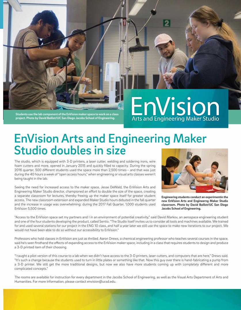
EnVision Arts and Engineering MakerStudio doubles in sizeThe studio, which is equipped with 3-D printers, a laser cutter, welding and soldering irons, wire foam cutters and more, opened in January 2015 and quickly filled to capacity. During the spring 2016 quarter, 500 di�erent students used the space more than 2,500 times-- and that was just during the 40 hours a week of “open access hours,” when engineering or visual arts classes weren’t being taught in the lab.
Seeing the need for increased access to the maker space, Jesse DeWald, the EnVision Arts and Engineering Maker Studio director, championed an e�ort to double the size of the space, creating a separate classroom for lectures, thereby freeing up the maker space itself for greater student access. The new classroom extension and expanded Maker Studio hours debuted in the fall quarter and the increase in usage was overwhelming: during the 2017 Fall Quarter, 1,000 students used EnVision 5,500 times.
"Access to the EnVision space set my partners and I in an environment of potential creativity,” said David Markov, an aerospace engineering student and one of the four students developing the product, called Sentio. “The Studio itself invites us to consider all tools and machines available. We trained for and used several stations for our project in the ENG 10 class, and half a year later we still use the space to make new iterations to our project. We would not have been able to do so without our accessibility to EnVision."
Professors who hold classes in EnVision are just as thrilled. Aaron Drews, a chemical engineering professor who teaches several courses in the space, said he’s seen firsthand the e�ects of expanding access to the EnVision maker space, including in a class that requires students to design and produce a 3-D printed item of their choosing.
“I taught a pilot version of this course to a lab when we didn’t have access to the 3-D printers, laser cutters, and computers that are here,” Drews said. “It’s such a change because the students used to turn in little plates or something like that. Now this guy over there is hand-fabricating a pump from a 3-D printer. We still get the more traditional designs, but now we also have more students coming up with completely di�erent and more complicated concepts.”
The rooms are available for instruction for every department in the Jacobs School of Engineering, as well as the Visual Arts Department of Arts and Humanities. For more information, please contact [email protected].
Students use the lab component of the EnVision maker space to work on a class project. Photo by David Baillot/UC San Diego Jacobs School of Engineering.
Engineering students conduct an experimentin the new EnVision Arts and Engineerng Maker Studio classroom. Photo by David Baillot/UC San Diego Jacobs School of Engineering.
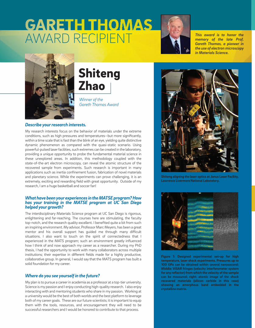
ShitengZhao
This award is to honor the memory of the late Prof. Gareth Thomas, a pioneer in the use of electron microscopy in Materials Science.
AWARD RECIPIENT
Winner of theGareth Thomas Award
Describe your research interests.My research interests focus on the behavior of materials under the extreme conditions, such as high pressures and temperatures—but more significantly, within a time scale that is fast than the blink of an eye, yielding quite distinctive dynamic phenomenon as compared with the quasi-static scenario. Using powerful-pulsed laser facilities, such extremes can be created in the laboratory, providing a unique opportunity to probe the fundamental material science in these unexplored areas. In addition, this methodology coupled with the state-of-the-art electron microscopy, can reveal the atomic structure of the recovered sample from experiments. Such research is important in many applications such as inertia confinement fusion, fabrication of novel materials and planetary science. While the experiments can prove challenging, it is an extremely, exciting and rewarding field with great opportunity. Outside of my research, I am a huge basketball and soccer fan!
What have been your experiences in the MATSE program? How has your training in the MATSE program at UC San Diego helped your growth?The interdisciplinary Materials Science program at UC San Diego is rigorous, enlightening and far-reaching. The courses here are stimulating, the faculty top-notch, and the research quality excellent. I benefited quite a bit from such an inspiring environment. My advisor, Professor Marc Meyers, has been a great mentor and his overall support has guided me through many di�icult situations. I also want to touch on the spirit of connectedness that I experienced in the MATS program; such an environment greatly influenced how I think of and now approach my career as a researcher. During my PhD thesis, I had the opportunity to work with many collaborators across multiple institutions; their expertise in di�erent fields made for a highly productive, collaborative group. In general, I would say that the MATS program has built a solid foundation for my career.
Where do you see yourself in the future?My plan is to pursue a career in academia as a professor at a top-tier university. Science is my passion and I enjoy conducting high-quality research. I also enjoy interacting with and mentoring students who share in my passion. Working at a university would be the best of both worlds and the best platform to leverage both of my career goals. These are our future scientists; it is important to equip them with the tools, resources, and encouragement they will need to be successful researchers and I would be honored to contribute to that process.
Figure 1: Designed experimental set-up for high temperature, laser shock experiments. Pressures up to 100 GPa can be obtained within several nanosecond; Middle: VISAR fringes (velocity interferometer system for any reflector) from which the velocity of the sample can be measured; right: atomic image of the shock recovered materials (silicon carbide in this case) showing an amorphous band embedded in the crystalline matrix.
Shiteng aligning the laser optics at Janus Laser Facility, Lawrence Livermore National Laboratory.
Michael Frazier Assistant ProfessorPh.D. University of Colorado Boulder
Frazier combines structural engineeringand materials science to create new materials for application such as long-distance signal transmission and enhanced vibration suppression. By employing theoretical approaches and experimental collaborations, he designs small-scale features of materials in order to control their responses at larger scales.
Nicholas BoechlerAssistant ProfessorPh.D. California Institute of Technology
Boechler uses fundamental principles to design materials with new mechanical properties. His work involves designing microstructures and nonlinear systems to create adaptive, resislient materials for applications including impact protection, signal processing, national defense, and civil infrastructure.
Abreu, Eliana Maria Amachraa, Mahdi Annapooranan, Raja Bopp, Steven Edward Breeden, Michael Christopher Brock, Je�rey Adams Cai, Jinze Cauchon, Alexander Jai Chang, Li-Yang Cheng, Diyi Dong, Gaoweiang Dong, Yongliang Dsouza, Macwin Savio Fahy, Kelsey Taylor Gasser, Albert Robert Getz, William
Gotlib, Oren Guo, Qianfeng Guo, Xingyu Han, Ke Hao, Tianduo He, Xuming Hong, Chenxi Hsieh, Yuchun Hu, Chongze Kim, Booseong Kumar, Rishi Eugene Lakshminarayanan, Balaji Lee, Elizabeth Marie Li, Feitong Li, Xiaoshi Li, Yifan
Lieng, Juelline Lin, Wen Yao Lin, Yuan Liu, Fangyu Lu, Yisheng Luo, Dong Oweimrin, Philip Farris Pelz, Joshua Stephan Pena, Rocio Marisol Petrova, Victoria Simeonova Qi, Yu Righi, Gaia Shelat, Kirtan V Shin, Haenara Sonar, Subodh Devendra Sun, Yan
Ueda, Scott Toshio Vakharia, Ved Sandip Vella, Gianmarco Wang, Edward Wisna, Gde Bimananda Mahardika Wu, Yunpeng Xing, Yiyuan Xiong, Xufan Xu, Feifan Yang, Qinglin Yin, Yijie Zhang, Huadong Zhang, Mingyuan Zhang, Yihui Zhang, Zichen Zhou, Yibo
Anne Pommier Assistant ProfessorPh.D. Institut des Sciences de la Terre d’Orléans, CNRS- University of Orléans
Pommier's research is dedicated to understanding how terrestrial planets work and especially the role of silicate and metallic melts in planetary interiors, from the scale of volcanic magma reservoirs to core-scale and planetary-scale processes.
Tod A. Pascal Assistant ProfessorPh.D. California Institute of Technology
Pascal develops and employs first principles electronic structure calculations and simulations to study the chemical physics of energy-related systems at the nanoscale. He is particularly interested in the molecular structure and dynamics of batteries, fuel cells and capacitors, disorder in condensed phase systems, and spectroscopy at interfaces.

Materials Science and Engineering ProgramUniversity of California, San Diego9500 Gilman Drive, Dept. 0418La Jolla, California 92093-0418
Nonprofit Org.U.S. Postage
PAIDSan Diego, CAPermit #1909
m a t s c i . u c s d . e d u
Doctoral student Tarah Sullivan and undergraduate researcher Alex Hung from Prof. Marc Meyers lab have created designs inspired by the resilient flight feathers of birds. While the feather vane appears as a cohesive material, on the micro- scale it is consists of components which are joined together through the mechanical interlocking of hooks and grooves. Designs inspired by this adhesive mechanism as well as other aspects of the feather were fabricated by 3D printing.
Back figure courtesy of UC San Diego Jacobs School of Engineering and the Meyers Lab