materials science copyright © 2019 ultrahigh thermal ... · ultrahigh thermal isolation across...
TRANSCRIPT

Vaziri et al., Sci. Adv. 2019; 5 : eaax1325 16 August 2019
S C I E N C E A D V A N C E S | R E S E A R C H A R T I C L E
1 of 7
M A T E R I A L S S C I E N C E
Ultrahigh thermal isolation across heterogeneously layered two-dimensional materialsSam Vaziri1*, Eilam Yalon1*†, Miguel Muñoz Rojo1‡, Saurabh V. Suryavanshi1, Huairuo Zhang2,3, Connor J. McClellan1, Connor S. Bailey1, Kirby K. H. Smithe1, Alexander J. Gabourie1, Victoria Chen1, Sanchit Deshmukh1, Leonid Bendersky3, Albert V. Davydov3, Eric Pop1,4,5§
Heterogeneous integration of nanomaterials has enabled advanced electronics and photonics applications. However, similar progress has been challenging for thermal applications, in part due to shorter wavelengths of heat carriers (phonons) compared to electrons and photons. Here, we demonstrate unusually high thermal isola-tion across ultrathin heterostructures, achieved by layering atomically thin two- dimensional (2D) materials. We realize artificial stacks of monolayer graphene, MoS2, and WSe2 with thermal resistance greater than 100 times thicker SiO2 and effective thermal conductivity lower than air at room temperature. Using Raman thermometry, we simultaneously identify the thermal resistance between any 2D monolayers in the stack. Ultrahigh thermal isolation is achieved through the mismatch in mass density and phonon density of states between the 2D layers. These thermal metamaterials are an example in the emerging field of phononics and could find applications where ultrathin thermal insulation is desired, in thermal energy harvesting, or for routing heat in ultracompact geometries.
INTRODUCTIONAdvanced electronic and photonic devices, like high-electron mobility transistors (1), quantum cascade lasers (2), and photonic bandgap crystals (3), take advantage of the fermionic nature of charge carriers for voltage gating or confinement, and of long photon wavelengths for interference. However, thermal nanoengineering and the emerging field of phononics offer fewer examples, despite high demand in heat management applications (4–6). This discrepancy is due to the short wavelengths of heat-carrying vibrations in solids, just a few nanometers for the dominant (median) phonon wavelength at room temperature (7, 8), which poses difficulties in nanofabrication at nearly atomic-scale dimensions. The bosonic nature of phonons, which cannot be voltage-gated like the charge carriers, also makes it challenging to actively control heat transport in solids.
Previous efforts to manipulate thermal properties of solids relied on nanolaminate films (9) and superlattices (10, 11) to reduce thermal conductivity below that of the constituent materials. These were achieved through structural disordering and high interface density, which introduce additional thermal resistance. Unusually low thermal conductivity was also found in silicon and germanium nanowires, from strong phonon-boundary scattering (12, 13). On the other hand, large thermal conductivities have been achieved in isotopi-cally pure materials, e.g., 12C diamond (14) or graphene (15), and in the cubic boron arsenide compound through reduced phonon scattering (16).
A new frontier is enabled by two-dimensional (2D) materials, which are sub-nanometer thin in single monolayers and thus amenable to control device behavior at atomic length scales (17). For example, heterogeneous 2D assemblies have been used for novel tunneling field-effect transistors (18) and ultrathin photovoltaics with high efficiency (19). Here, we use van der Waals (vdW) as-sembly of atomically thin 2D layers to achieve unusually high ther-mal resistance across their heterostructures. Specifically, we show a thermal resistance equivalent to that of ~300-nm SiO2 across sub–2-nm-thin vdW heterostructures with clean, residue-free interfaces. We also demonstrate the ability of tailoring thermal properties at atomic-scale dimensions, on the order of the phonon wavelength, by layering heterogeneous 2D monolayers with different atomic mass densities and vibrational modes. Such structures form new phononic metamaterials with unusual properties not commonly found in nature. These also represent a unique application of 2D materials and their weak vdW interactions, which can be assembled (here, to block or guide the flow of heat) without the requirement of epitaxially matched interfaces.
RESULTSMicrostructural and optical characteristicsFigure 1A shows the schematic cross-section of a four-layer hetero-structure with (from top to bottom) graphene (Gr) on MoSe2, MoS2, and WSe2, all on a SiO2/Si substrate. The Raman laser illustrated is used for simultaneously probing the individual layers in the stack, with single-layer accuracy. All 2D materials are monolayers, separately grown by chemical vapor deposition (CVD) (20) and transferred while avoiding polymer and other residues. (Details are provided in Materials and Methods and section S1.) To confirm microstructural, thermal, and electrical uniformity of the hetero-structures, we use scanning transmission electron microscopy (STEM), photoluminescence (PL) spectroscopy, Kelvin probe microscopy (KPM), scanning thermal microscopy (SThM), as well as Raman spectroscopy and thermometry.
1Department of Electrical Engineering, Stanford University, Stanford, CA 94305, USA. 2Theiss Research Inc., La Jolla, CA 92037, USA. 3Materials Science and Engineering Division, National Institute of Standards and Technology (NIST), Gaithersburg, MA 20899, USA. 4Department of Materials Science and Engineering, Stanford University, Stanford, CA 94305, USA. 5Precourt Institute for Energy, Stanford University, Stanford, CA 94305, USA.*These authors contributed equally to this work.†Present address: Department of Electrical Engineering, Technion-Israel Institute of Technology, Haifa 32000, Israel.‡Present address: Department of Thermal and Fluid Engineering, University of Twente, 7500 AE Enschede, Netherlands.§Corresponding author. Email: [email protected]
Copyright © 2019 The Authors, some rights reserved; exclusive licensee American Association for the Advancement of Science. No claim to original U.S. Government Works. Distributed under a Creative Commons Attribution NonCommercial License 4.0 (CC BY-NC).
on June 5, 2020http://advances.sciencem
ag.org/D
ownloaded from

Vaziri et al., Sci. Adv. 2019; 5 : eaax1325 16 August 2019
S C I E N C E A D V A N C E S | R E S E A R C H A R T I C L E
2 of 7
Figure 1B shows the Raman spectrum of such a Gr/MoSe2/MoS2/WSe2 heterostructure on SiO2/Si at the location of the red dot in the inset. It reveals the signature of every 2D material monolayer in the stack, as well as that of the Si substrate. This is a unique strength of the Raman technique, allowing us to identify each material with nonoverlapping Raman modes and to measure its individual temperature. All characteristic Raman peaks of the constituent materials are observed (see Materials and Methods) (21), except for the D peak of graphene, indicating negligible disorder.
Figure 1 (C to F) shows cross-sectional atomic-resolution annular dark-field STEM (ADF-STEM) images of our Gr/MoSe2/MoS2/WSe2 (Fig. 1C) and Gr/MoS2/WSe2 (Fig. 1, D to F) heterostructures with dif-ferent lattice orientation alignments. Multiple STEM images reveal atomically intimate vdW gaps without contaminants, allowing us to observe the total thickness of these heterostructures, e.g., just below 2 nm for a three-layer stack (also see fig. S2). The interlayer coupling is further confirmed over larger areas by PL spectroscopy (Fig. 1G). The PL signal of individual layers in the heterostructure is substantially quenched (over one order of magnitude) compared to isolated mono-layers on the same substrate. This PL quenching is attributed to an interlayer charge transfer process due to intimate interlayer coupling, which becomes even stronger after annealing (see section S3) (22).
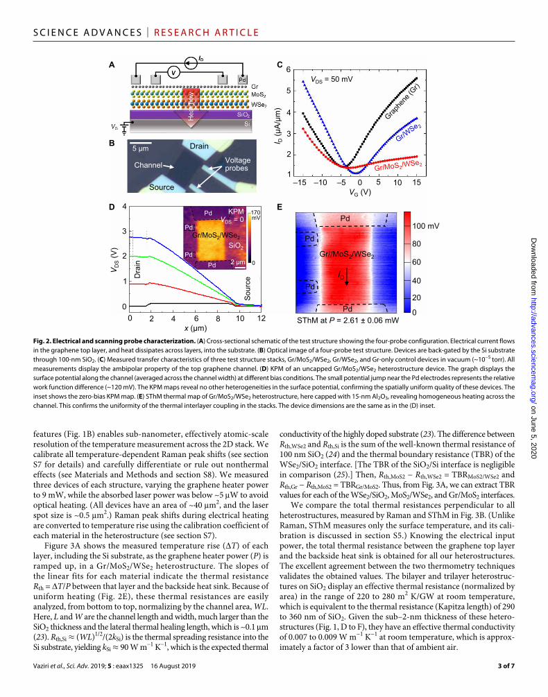
Electrical characteristics and thermal uniformityTo measure heat flow perpendicular to the atomic planes of the hetero-structures, we pattern the stacks in the shape of four-probe electrical
devices (see Materials and Methods). The top graphene layer is con-tacted by Pd electrodes and used as a nearly transparent Joule heater for the Raman thermometry measurements. This electrical heating method enables accurate quantification of the input power (23), whereas a purely optical heating method (24) would be more challeng-ing without knowing the absorption coefficients of individual layers.
Figure 2 (A and B) displays the schematic of the four-probe measurement and the top view of a test structure, respectively. Figure 2C shows the measured back-gated transfer characteristics of three devices, one with only graphene and two with stacks of Gr/WSe2 and Gr/MoSe2/WSe2. These all show the well-known ambipolar behavior of graphene due to the absence of an energy bandgap. They also confirm that current conduction and heating occur in the top graphene layer, its electrical conductivity being orders of magnitude higher than MoS2 and WSe2 (see section S6). To demon-strate the uniformity of these devices, we also use KPM and SThM surface characterization. Figure 2D displays KPM measurements taken along the device at various VDS, revealing smooth and linear potential distributions. Figure 2E shows an SThM map of the elec-trically heated Gr/MoS2/WSe2 channel, displaying uniform surface heating with high spatial resolution (see section S4).
Thermometry of the vdW heterostructuresWhile SThM confirms the surface temperature uniformity of our devices, we used Raman spectroscopy to quantify the temperature of each individual layer. The spectral separation of key Raman
Fig. 1. Optical and STEM characterization of vdW heterostructures. (A) Cross-section schematic of Gr/MoSe2/MoS2/WSe2 sandwich on SiO2/Si substrate, with the incident Raman laser. (B) Raman spectrum of such a heterostructure at the spot indicated by the red dot in the inset optical image. Raman signatures of all materials in the stack are obtained simultaneously. The graphene Raman spectrum is flattened to exclude the MoS2 photoluminescence (PL) effect. arb.u., arbitrary units. (C to F) STEM cross-sectional images of four-layer (C) and three-layer (D to F) heterostructures on SiO2. In (D), MoSe2 and WSe2 are approximately aligned along the 1H [100] zone axis, and in (E and F), the layers are misaligned by ~21° with respect to the 1H [100] zone axis. The monolayer graphene on top of each heterostructure is hard to discern due to the much lower atomic number of the carbon atoms. (G) PL spectra of monolayer MoS2, monolayer WSe2, and a Gr/MoS2/WSe2 heterostructure after annealing. The PL is strongly quenched in the heterostructure due to intimate interlayer coupling.
on June 5, 2020http://advances.sciencem
ag.org/D
ownloaded from
Vaziri et al., Sci. Adv. 2019; 5 : eaax1325 16 August 2019
S C I E N C E A D V A N C E S | R E S E A R C H A R T I C L E
3 of 7
features (Fig. 1B) enables sub-nanometer, effectively atomic-scale resolution of the temperature measurement across the 2D stack. We calibrate all temperature-dependent Raman peak shifts (see section S7 for details) and carefully differentiate or rule out nonthermal effects (see Materials and Methods and section S8). We measured three devices of each structure, varying the graphene heater power to 9 mW, while the absorbed laser power was below ~5 W to avoid optical heating. (All devices have an area of ~40 m2, and the laser spot size is ~0.5 m2.) Raman peak shifts during electrical heating are converted to temperature rise using the calibration coefficient of each material in the heterostructure (see section S7).
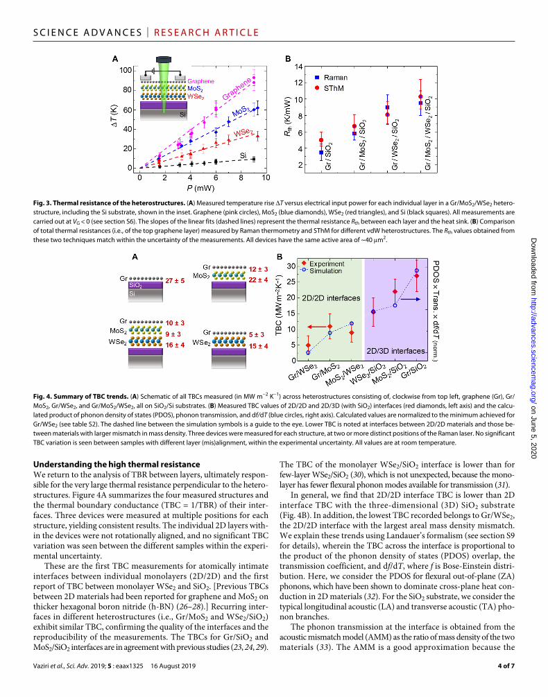
Figure 3A shows the measured temperature rise (T) of each layer, including the Si substrate, as the graphene heater power (P) is ramped up, in a Gr/MoS2/WSe2 heterostructure. The slopes of the linear fits for each material indicate the thermal resistance Rth = T/P between that layer and the backside heat sink. Because of uniform heating (Fig. 2E), these thermal resistances are easily analyzed, from bottom to top, normalizing by the channel area, WL. Here, L and W are the channel length and width, much larger than the SiO2 thickness and the lateral thermal healing length, which is ~0.1 m (23). Rth,Si ≈ (WL)1/2/(2kSi) is the thermal spreading resistance into the Si substrate, yielding kSi ≈ 90 W m−1 K−1, which is the expected thermal
conductivity of the highly doped substrate (23). The difference between Rth,WSe2 and Rth,Si is the sum of the well-known thermal resistance of 100 nm SiO2 (24) and the thermal boundary resistance (TBR) of the WSe2/SiO2 interface. [The TBR of the SiO2/Si interface is negligible in comparison (25).] Then, Rth,MoS2 − Rth,WSe2 = TBRMoS2/WSe2 and Rth,Gr − Rth,MoS2 = TBRGr/MoS2. Thus, from Fig. 3A, we can extract TBR values for each of the WSe2/SiO2, MoS2/WSe2, and Gr/MoS2 interfaces.
We compare the total thermal resistances perpendicular to all heterostructures, measured by Raman and SThM in Fig. 3B. (Unlike Raman, SThM measures only the surface temperature, and its cali-bration is discussed in section S5.) Knowing the electrical input power, the total thermal resistance between the graphene top layer and the backside heat sink is obtained for all our heterostructures. The excellent agreement between the two thermometry techniques validates the obtained values. The bilayer and trilayer heterostruc-tures on SiO2 display an effective thermal resistance (normalized by area) in the range of 220 to 280 m2 K/GW at room temperature, which is equivalent to the thermal resistance (Kapitza length) of 290 to 360 nm of SiO2. Given the sub–2-nm thickness of these hetero-structures (Fig. 1, D to F), they have an effective thermal conductivity of 0.007 to 0.009 W m−1 K−1 at room temperature, which is approx-imately a factor of 3 lower than that of ambient air.
1
2
3
4
5
6
–15 –10 –5 0 15105
I D(µ
A/µ
m)
VG (V)
Pd
Pd
PdPd
2 µm
Gr/MoS2/WSe2
SiO2
Dra
in
Sou
rce
VD
S(V
)
x (µm)
0
1
2
3
4
2 4 6 8 10 12
KPMVDS = 0
Voltage probes
Source
Drain
Channel
5 µm
VDS = 50 mV
0
C
100 mV
Gr//MoS2/WSe2
Pd
Pd
Pd
Pd
80
60
40
20
0
E
ID
SThM at P = 2.61 ± 0.06 mW
A
D
B
0
170mV
Fig. 2. Electrical and scanning probe characterization. (A) Cross-sectional schematic of the test structure showing the four-probe configuration. Electrical current flows in the graphene top layer, and heat dissipates across layers, into the substrate. (B) Optical image of a four-probe test structure. Devices are back-gated by the Si substrate through 100-nm SiO2. (C) Measured transfer characteristics of three test structure stacks, Gr/MoS2/WSe2, Gr/WSe2, and Gr-only control devices in vacuum (~10−5 torr). All measurements display the ambipolar property of the top graphene channel. (D) KPM of an uncapped Gr/MoS2/WSe2 heterostructure device. The graph displays the surface potential along the channel (averaged across the channel width) at different bias conditions. The small potential jump near the Pd electrodes represents the relative work function difference (~120 mV). The KPM maps reveal no other heterogeneities in the surface potential, confirming the spatially uniform quality of these devices. The inset shows the zero-bias KPM map. (E) SThM thermal map of Gr/MoS2/WSe2 heterostructure, here capped with 15-nm Al2O3, revealing homogeneous heating across the channel. This confirms the uniformity of the thermal interlayer coupling in the stacks. The device dimensions are the same as in the (D) inset. on June 5, 2020
http://advances.sciencemag.org/
Dow
nloaded from
Vaziri et al., Sci. Adv. 2019; 5 : eaax1325 16 August 2019
S C I E N C E A D V A N C E S | R E S E A R C H A R T I C L E
4 of 7
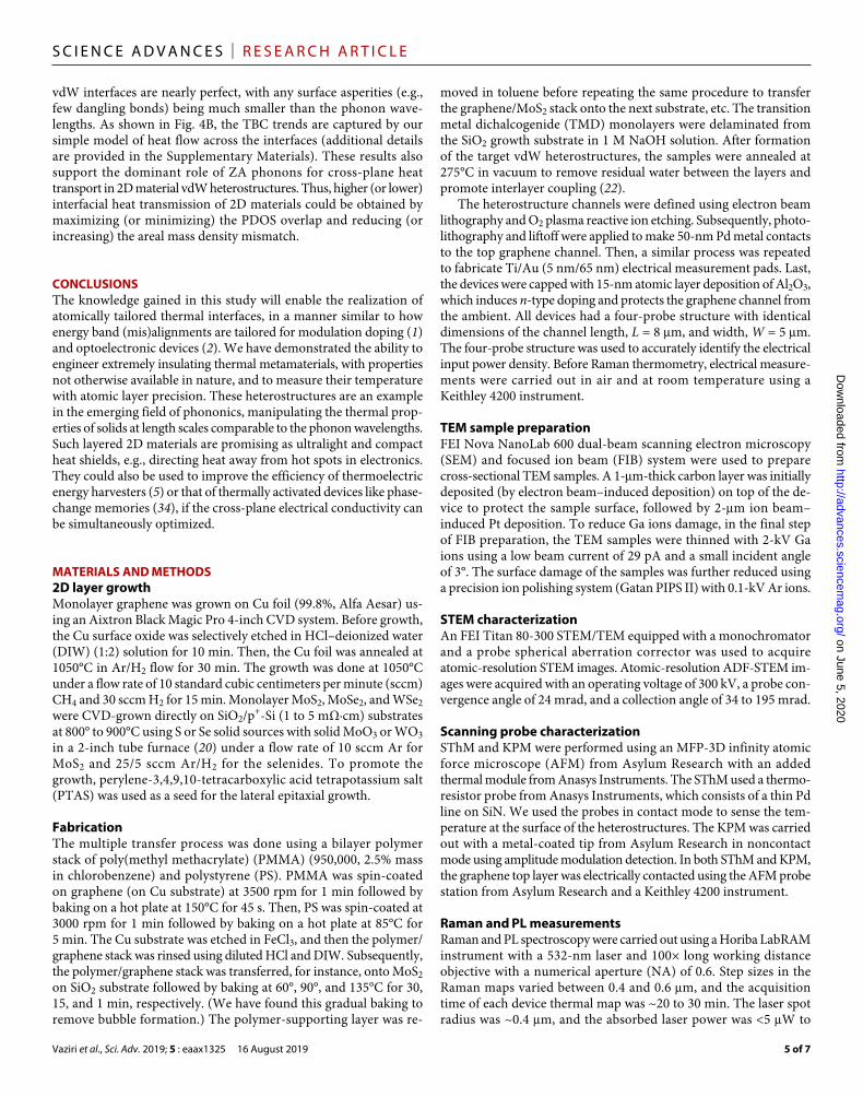
Understanding the high thermal resistanceWe return to the analysis of TBR between layers, ultimately respon-sible for the very large thermal resistance perpendicular to the hetero-structures. Figure 4A summarizes the four measured structures and the thermal boundary conductance (TBC = 1/TBR) of their inter-faces. Three devices were measured at multiple positions for each structure, yielding consistent results. The individual 2D layers with-in the devices were not rotationally aligned, and no significant TBC variation was seen between the different samples within the experi-mental uncertainty.
These are the first TBC measurements for atomically intimate interfaces between individual monolayers (2D/2D) and the first report of TBC between monolayer WSe2 and SiO2. [Previous TBCs between 2D materials had been reported for graphene and MoS2 on thicker hexagonal boron nitride (h-BN) (26–28).] Recurring inter-faces in different heterostructures (i.e., Gr/MoS2 and WSe2/SiO2) exhibit similar TBC, confirming the quality of the interfaces and the reproducibility of the measurements. The TBCs for Gr/SiO2 and MoS2/SiO2 interfaces are in agreement with previous studies (23, 24, 29).
The TBC of the monolayer WSe2/SiO2 interface is lower than for few-layer WSe2/SiO2 (30), which is not unexpected, because the mono-layer has fewer flexural phonon modes available for transmission (31).
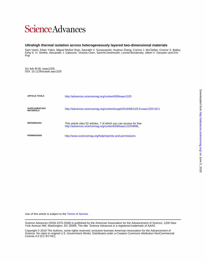
In general, we find that 2D/2D interface TBC is lower than 2D interface TBC with the three-dimensional (3D) SiO2 substrate (Fig. 4B). In addition, the lowest TBC recorded belongs to Gr/WSe2, the 2D/2D interface with the largest areal mass density mismatch. We explain these trends using Landauer’s formalism (see section S9 for details), wherein the TBC across the interface is proportional to the product of the phonon density of states (PDOS) overlap, the transmission coefficient, and df/dT, where f is Bose-Einstein distri-bution. Here, we consider the PDOS for flexural out-of-plane (ZA) phonons, which have been shown to dominate cross-plane heat con-duction in 2D materials (32). For the SiO2 substrate, we consider the typical longitudinal acoustic (LA) and transverse acoustic (TA) pho-non branches.
The phonon transmission at the interface is obtained from the acoustic mismatch model (AMM) as the ratio of mass density of the two materials (33). The AMM is a good approximation because the
Fig. 3. Thermal resistance of the heterostructures. (A) Measured temperature rise T versus electrical input power for each individual layer in a Gr/MoS2/WSe2 hetero-structure, including the Si substrate, shown in the inset. Graphene (pink circles), MoS2 (blue diamonds), WSe2 (red triangles), and Si (black squares). All measurements are carried out at VG < 0 (see section S6). The slopes of the linear fits (dashed lines) represent the thermal resistance Rth between each layer and the heat sink. (B) Comparison of total thermal resistances (i.e., of the top graphene layer) measured by Raman thermometry and SThM for different vdW heterostructures. The Rth values obtained from these two techniques match within the uncertainty of the measurements. All devices have the same active area of ~40 m2.
Fig. 4. Summary of TBC trends. (A) Schematic of all TBCs measured (in MW m−2 K−1) across heterostructures consisting of, clockwise from top left, graphene (Gr), Gr/MoS2, Gr/WSe2, and Gr/MoS2/WSe2, all on SiO2/Si substrates. (B) Measured TBC values of 2D/2D and 2D/3D (with SiO2) interfaces (red diamonds, left axis) and the calcu-lated product of phonon density of states (PDOS), phonon transmission, and df/dT (blue circles, right axis). Calculated values are normalized to the minimum achieved for Gr/WSe2 (see table S2). The dashed line between the simulation symbols is a guide to the eye. Lower TBC is noted at interfaces between 2D/2D materials and those be-tween materials with larger mismatch in mass density. Three devices were measured for each structure, at two or more distinct positions of the Raman laser. No significant TBC variation is seen between samples with different layer (mis)alignment, within the experimental uncertainty. All values are at room temperature.
on June 5, 2020http://advances.sciencem
ag.org/D
ownloaded from
Vaziri et al., Sci. Adv. 2019; 5 : eaax1325 16 August 2019
S C I E N C E A D V A N C E S | R E S E A R C H A R T I C L E
5 of 7
vdW interfaces are nearly perfect, with any surface asperities (e.g., few dangling bonds) being much smaller than the phonon wave-lengths. As shown in Fig. 4B, the TBC trends are captured by our simple model of heat flow across the interfaces (additional details are provided in the Supplementary Materials). These results also support the dominant role of ZA phonons for cross-plane heat transport in 2D material vdW heterostructures. Thus, higher (or lower) interfacial heat transmission of 2D materials could be obtained by maximizing (or minimizing) the PDOS overlap and reducing (or increasing) the areal mass density mismatch.
CONCLUSIONSThe knowledge gained in this study will enable the realization of atomically tailored thermal interfaces, in a manner similar to how energy band (mis)alignments are tailored for modulation doping (1) and optoelectronic devices (2). We have demonstrated the ability to engineer extremely insulating thermal metamaterials, with properties not otherwise available in nature, and to measure their temperature with atomic layer precision. These heterostructures are an example in the emerging field of phononics, manipulating the thermal prop-erties of solids at length scales comparable to the phonon wavelengths. Such layered 2D materials are promising as ultralight and compact heat shields, e.g., directing heat away from hot spots in electronics. They could also be used to improve the efficiency of thermoelectric energy harvesters (5) or that of thermally activated devices like phase- change memories (34), if the cross-plane electrical conductivity can be simultaneously optimized.
MATERIALS AND METHODS2D layer growthMonolayer graphene was grown on Cu foil (99.8%, Alfa Aesar) us-ing an Aixtron Black Magic Pro 4-inch CVD system. Before growth, the Cu surface oxide was selectively etched in HCl–deionized water (DIW) (1:2) solution for 10 min. Then, the Cu foil was annealed at 1050°C in Ar/H2 flow for 30 min. The growth was done at 1050°C under a flow rate of 10 standard cubic centimeters per minute (sccm) CH4 and 30 sccm H2 for 15 min. Monolayer MoS2, MoSe2, and WSe2 were CVD-grown directly on SiO2/p+-Si (1 to 5 mΩ·cm) substrates at 800° to 900°C using S or Se solid sources with solid MoO3 or WO3 in a 2-inch tube furnace (20) under a flow rate of 10 sccm Ar for MoS2 and 25/5 sccm Ar/H2 for the selenides. To promote the growth, perylene-3,4,9,10-tetracarboxylic acid tetrapotassium salt (PTAS) was used as a seed for the lateral epitaxial growth.
FabricationThe multiple transfer process was done using a bilayer polymer stack of poly(methyl methacrylate) (PMMA) (950,000, 2.5% mass in chlorobenzene) and polystyrene (PS). PMMA was spin-coated on graphene (on Cu substrate) at 3500 rpm for 1 min followed by baking on a hot plate at 150°C for 45 s. Then, PS was spin-coated at 3000 rpm for 1 min followed by baking on a hot plate at 85°C for 5 min. The Cu substrate was etched in FeCl3, and then the polymer/graphene stack was rinsed using diluted HCl and DIW. Subsequently, the polymer/graphene stack was transferred, for instance, onto MoS2 on SiO2 substrate followed by baking at 60°, 90°, and 135°C for 30, 15, and 1 min, respectively. (We have found this gradual baking to remove bubble formation.) The polymer-supporting layer was re-
moved in toluene before repeating the same procedure to transfer the graphene/MoS2 stack onto the next substrate, etc. The transition metal dichalcogenide (TMD) monolayers were delaminated from the SiO2 growth substrate in 1 M NaOH solution. After formation of the target vdW heterostructures, the samples were annealed at 275°C in vacuum to remove residual water between the layers and promote interlayer coupling (22).
The heterostructure channels were defined using electron beam lithography and O2 plasma reactive ion etching. Subsequently, photo-lithography and liftoff were applied to make 50-nm Pd metal contacts to the top graphene channel. Then, a similar process was repeated to fabricate Ti/Au (5 nm/65 nm) electrical measurement pads. Last, the devices were capped with 15-nm atomic layer deposition of Al2O3, which induces n-type doping and protects the graphene channel from the ambient. All devices had a four-probe structure with identical dimensions of the channel length, L = 8 m, and width, W = 5 m. The four-probe structure was used to accurately identify the electrical input power density. Before Raman thermometry, electrical measure-ments were carried out in air and at room temperature using a Keithley 4200 instrument.
TEM sample preparationFEI Nova NanoLab 600 dual-beam scanning electron microscopy (SEM) and focused ion beam (FIB) system were used to prepare cross-sectional TEM samples. A 1-m-thick carbon layer was initially deposited (by electron beam–induced deposition) on top of the de-vice to protect the sample surface, followed by 2-m ion beam–induced Pt deposition. To reduce Ga ions damage, in the final step of FIB preparation, the TEM samples were thinned with 2-kV Ga ions using a low beam current of 29 pA and a small incident angle of 3°. The surface damage of the samples was further reduced using a precision ion polishing system (Gatan PIPS II) with 0.1-kV Ar ions.
STEM characterizationAn FEI Titan 80-300 STEM/TEM equipped with a monochromator and a probe spherical aberration corrector was used to acquire atomic-resolution STEM images. Atomic-resolution ADF-STEM im-ages were acquired with an operating voltage of 300 kV, a probe con-vergence angle of 24 mrad, and a collection angle of 34 to 195 mrad.
Scanning probe characterizationSThM and KPM were performed using an MFP-3D infinity atomic force microscope (AFM) from Asylum Research with an added thermal module from Anasys Instruments. The SThM used a thermo-resistor probe from Anasys Instruments, which consists of a thin Pd line on SiN. We used the probes in contact mode to sense the tem-perature at the surface of the heterostructures. The KPM was carried out with a metal-coated tip from Asylum Research in noncontact mode using amplitude modulation detection. In both SThM and KPM, the graphene top layer was electrically contacted using the AFM probe station from Asylum Research and a Keithley 4200 instrument.
Raman and PL measurementsRaman and PL spectroscopy were carried out using a Horiba LabRAM instrument with a 532-nm laser and 100× long working distance objective with a numerical aperture (NA) of 0.6. Step sizes in the Raman maps varied between 0.4 and 0.6 m, and the acquisition time of each device thermal map was ~20 to 30 min. The laser spot radius was ~0.4 m, and the absorbed laser power was <5 W to
on June 5, 2020http://advances.sciencem
ag.org/D
ownloaded from

Vaziri et al., Sci. Adv. 2019; 5 : eaax1325 16 August 2019
S C I E N C E A D V A N C E S | R E S E A R C H A R T I C L E
6 of 7
avoid laser heating in excess of the electrical heating and to maintain negligible photocurrent. The Raman spectra of the four-layer hetero-structure of Gr/MoSe2/MoS2/WSe2 (Fig. 1B) showed peaks at 241.5 and 404.6 cm−1 corresponding to out-of-plane A1′ modes for MoSe2 and MoS2, respectively. The in-plane E′ modes for MoSe2 and MoS2 were represented by the peaks at 286.5 and 383.1 cm−1, respectively. Monolayer WSe2 showed the characteristic degenerate peak at 249.4 cm−1, which included both A1′ and E′, while the 2LA peak was at 259.3 cm−1. Furthermore, the G and G′ (sometimes called 2D) peaks of monolayer graphene were at 1585.3 and 2690.5 cm−1, re-spectively. We used the graphene G peak and the TMD out-of-plane modes for thermometry because they were less sensitive to strain.
For temperature-dependent Raman shift calibration, we used a Linkam THMS600 stage and carefully differentiated effects of strain (e.g., during the calibration on hot stage) and shifts due to electrical bias (gating effect from the substrate), following the calibration pro-cedure outlined in section S7. The obtained Raman temperature maps were uniform (see section S6), similar to the SThM measure-ments shown in section S4. The uniform heating in the channel indicated that there was no measurable nonuniform doping or pinch-off, which simplified the extraction of interlayer TBC. Changes in the measured current along the graphene channel during mapping were smaller than 5%. All thermometry measurements were per-formed in ambient and at room temperature.
SUPPLEMENTARY MATERIALSSupplementary material for this article is available at http://advances.sciencemag.org/cgi/content/full/5/8/eaax1325/DC1Section S1. Multiple transfer techniqueSection S2. Atomic-resolution ADF-STEMSection S3. PL quenching in 2D heterostructuresSection S4. SThM thermal mapsSection S5. SThM temperature calibrationSection S6. Raman temperature mapsSection S7. Temperature-dependent Raman coefficientsSection S8. Non–temperature-related Raman peak shiftsSection S9. Thermal transport modeling and analysisFig. S1. Transfer process and optical images.Fig. S2. Atomic-resolution ADF-STEM images.Fig. S3. PL quenching.Fig. S4. Uniform heating maps.Fig. S5. SThM calibration by metal line heaters.Fig. S6. Raman maps.Fig. S7. Temperature-dependent Raman coefficients.Fig. S8. Raman shift dependence on doping and electrical gating.Fig. S9. PDOS overlap.Table S1. Material parameters.Table S2. TBC comparison.References (35–55)
REFERENCES AND NOTES 1. T. Mimura, S. Hiyamizu, T. Fujii, K. Nanbu, A new field-effect transistor
with selectively doped GaAs/n-AlxGa1-xAs heterojunctions. Jpn. J. Appl. Phys. 19, L225–L227 (1980).
2. J. Faist, F. Capasso, D. L. Sivco, C. Sirtori, A. L. Hutchinson, A. Y. Cho, Quantum cascade laser. Science 264, 553–556 (1994).
3. E. Yablonovitch, Photonic band-gap crystals. J. Phys. Condens. Matter 5, 2443–2460 (1993).
4. M. Maldovan, Sound and heat revolutions in phononics. Nature 503, 209–217 (2013). 5. M. S. Dresselhaus, G. Chen, M. Y. Tang, R. G. Yang, H. Lee, D. Z. Wang, Z. F. Ren,
J.-P. Fleurial, P. Gogna, New directions for low-dimensional thermoelectric materials. Adv. Mater. 19, 1043–1053 (2007).
6. P. Ball, Computer engineering: Feeling the heat. Nature 492, 174–176 (2012). 7. J. Mair, R. Anufriev, R. Yanagisawa, A. Ramiere, S. Volz, M. Nomura, Heat conduction
tuning by wave nature of phonons. Sci. Adv. 3, e1700027 (2017).
8. A. Sood, F. Xiong, S. Chen, R. Cheaito, F. Lian, M. Asheghi, Y. Cui, D. Donadio, K. E. Goodson, E. Pop, Quasi-ballistic thermal transport across MoS2 thin films. Nano Lett. 19, 2434–2442 (2019).
9. R. M. Costescu, D. G. Cahill, F. H. Fabreguette, Z. A. Sechrist, S. M. George, Ultra-low thermal conductivity in W/Al2O3 nanolaminates. Science 303, 989–990 (2004).
10. C. Chiritescu, D. G. Cahill, N. Nguyen, D. Johnson, A. Bodapati, P. Keblinski, P. Zschack, Ultralow thermal conductivity in disordered, layered WSe2 crystals. Science 315, 351–353 (2007).
11. Z. Li, S. Bauers, N. Poudel, D. Hamann, X. Wang, D. S. Choi, K. Esfarjani, L. Shi, D. C. Johnson, S. B. Cronin, Cross-plane seebeck coefficient measurement of Misfit layered compounds (SnSe)n(TiSe2)n, (n=1,3,4,5). Nano Lett. 17, 1978–1986 (2017).
12. M. G. Ghossoub, K. V. Valavala, M. Seong, B. Azeredo, K. Hsu, J. S. Sadhu, P. K. Singh, S. Sinha, Spectral phonon scattering from sub-10 nm surface roughness wavelengths in metal-assisted chemically etched Si nanowires. Nano Lett. 13, 1564–1571 (2013).
13. P. N. Martin, Z. Aksamija, E. Pop, U. Ravaioli, Reduced thermal conductivity in nanoengineered rough Ge and GaAs nanowires. Nano Lett. 10, 1120–1124 (2010).
14. T. R. Anthony, W. F. Banholzer, J. F. Fleischer, L. Wei, P. K. Kuo, R. L. Thomas, R. W. Pryor, Thermal diffusivity of isotopically enriched 12C diamond. Phys. Rev. B 42, 1104–1111 (1990).
15. S. Chen, Q. Wu, C. Mishra, J. Kang, H. Zhang, K. Cho, W. Cai, A. A. Balandin, R. S. Ruoff, Thermal conductivity of isotopically modified graphene. Nat. Mater. 11, 203–207 (2012).
16. S. Li, Q. Zheng, Y. Lv, X. Liu, X. Wang, P. Y. Huang, D. G. Cahill, B. Lv, High thermal conductivity in cubic boron arsenide crystals. Science 361, 579–581 (2018).
17. K. S. Novoselov, A. Mishchenko, A. Carvalho, A. H. C. Neto, 2D materials and van der Waals heterostructures. Science 353, aac9439 (2016).
18. L. Britnell, R. V. Gorbachev, R. Jalil, B. D. Belle, F. Schedin, A. Mishchenko, T. Georgiou, M. I. Katsnelson, L. Eaves, S. V. Morozov, N. M. R. Peres, J. Leist, A. K. Geim, K. S. Novoselov, L. A. Ponomarenko, Field-effect tunneling transistor based on vertical graphene heterostructures. Science 335, 947–950 (2012).
19. W. Zhang, Q. Wang, Y. Chen, Z. Wang, A. T. S. Wee, Van der Waals stacked 2D layered materials for optoelectronics. 2D Mater. 3, 022001 (2016).
20. K. K. H. Smithe, C. D. English, S. V. Suryavanshi, E. Pop, Intrinsic electrical transport and performance projections of synthetic monolayer MoS2 devices. 2D Mater. 4, 011009 (2017).
21. X. Zhang, X.-F. Qiao, W. Shi, J.-B. Wu, D.-S. Jiang, P.-H. Tan, Phonon and Raman scattering of two-dimensional transition metal dichalcogenides from monolayer, multilayer to bulk material. Chem. Soc. Rev. 44, 2757–2785 (2015).
22. M.-H. Chiu, M.-Y. Li, W. Zhang, W.-T. Hsu, W.-H. Chang, M. Terrones, H. Terrones, L.-J. Li, Spectroscopic signatures for interlayer coupling in MoS2-WSe2 van der Waals stacking. ACS Nano 8, 9649–9656 (2014).
23. E. Yalon, C. J. McClellan, K. K. H. Smithe, M. Muñoz Rojo, R. L. Xu, S. V. Suryavanshi, A. J. Gabourie, C. M. Neumann, F. Xiong, A. B. Farimani, E. Pop, Energy dissipation in monolayer MoS2 Electronics. Nano Lett. 17, 3429–3433 (2017).
24. E. Yalon, Ö. B. Aslan, K. K. H. Smithe, C. J. McClellan, S. V. Suryavanshi, F. Xiong, A. Sood, C. M. Neumann, X. Xu, K. E. Goodson, T. F. Heinz, E. Pop, Temperature-dependent thermal boundary conductance of monolayer MoS2 by Raman thermometry. ACS Appl. Mater. Interfaces 9, 43013–43020 (2017).
25. J. Kimling, A. Philippi-Kobs, J. Jacobsohn, H. P. Oepen, D. G. Cahill, Thermal conductance of interfaces with amorphous SiO2 measured by time-resolved magneto-optic Kerr-effect thermometry. Phys. Rev. B 95, 184305 (2017).
26. C.-C. Chen, Z. Li, L. Shi, S. B. Cronin, Thermal interface conductance across a graphene/hexagonal boron nitride heterojunction. Appl. Phys. Lett. 104, 081908 (2014).
27. D. Kim, H. Kim, W. S. Yun, K. Watanabe, T. Taniguchi, H. Rho, M.-H. Bae, Energy dissipation mechanism revealed by spatially resolved Raman thermometry of graphene/hexagonal boron nitride heterostructure devices. 2D Mater. 5, 025009 (2018).
28. Y. Liu, Z.-Y. Ong, J. Wu, Y. Zhao, K. Watanabe, T. Taniguchi, D. Chi, G. Zhang, J. T. L. Thong, C.-W. Qiu, K. Hippalgaonkar, Thermal conductance of the 2D MoS2/h-BN and graphene/h-BN interfaces. Sci. Rep. 7, 43886 (2017).
29. M. Freitag, M. Steiner, Y. Martin, V. Perebeinos, Z. Chen, J. C. Tsang, P. Avouris, Energy dissipation in graphene field-effect transistors. Nano Lett. 9, 1883–1888 (2009).
30. A. Behranginia, Z. Hemmat, A. K. Majee, C. J. Foss, P. Yasaei, Z. Aksamija, A. Salehi-Khojin, Power dissipation of WSe2 field-effect transistors probed by low-frequency Raman thermometry. ACS Appl. Mater. Interfaces 10, 24892–24898 (2018).
31. Z.-Y. Ong, Thickness-dependent Kapitza resistance in multilayered graphene and other two-dimensional crystals. Phys. Rev. B 95, 155309 (2017).
32. Z.-Y. Ong, B. Qiu, S. Xu, X. Ruan, E. Pop, Flexural resonance mechanism of thermal transport across graphene-SiO2 interfaces. J. Appl. Phys. 123, 115107 (2018).
33. W. A. Little, The transport of heat between dissimilar solids at low temperatures, in From High-Temperature Superconductivity to Microminiature Refrigeration, B. Cabrera, H. Gutfreund, V. Kresin, Eds. (Springer, 1996), pp. 15–30.
34. C. M. Neumann, K. L. Okabe, E. Yalon, R. W. Grady, H.-S. P. Wong, E. Pop, Engineering thermal and electrical interface properties of phase change memory with monolayer MoS2. Appl. Phys. Lett. 114, 082103 (2019).
on June 5, 2020http://advances.sciencem
ag.org/D
ownloaded from

Vaziri et al., Sci. Adv. 2019; 5 : eaax1325 16 August 2019
S C I E N C E A D V A N C E S | R E S E A R C H A R T I C L E
7 of 7
35. X. Hong, J. Kim, S.-F. Shi, Y. Zhang, C. Jin, Y. Sun, S. Tongay, J. Wu, Y. Zhang, F. Wang, Ultrafast charge transfer in atomically thin MoS2/WS2 heterostructures. Nat. Nanotechnol. 9, 682–686 (2014).
36. B. Peng, G. Yu, X. Liu, B. Liu, X. Liang, L. Bi, L. Deng, T. C. Sum, K. P. Loh, Ultrafast charge transfer in MoS2/WSe2 p-n heterojunction. 2D Mater. 3, 025020 (2016).
37. C. H. Lui, Z. P. Ye, C. Ji, K.-C. Chiu, C.-T. Chou, T. I. Andersen, C. Means-Shively, H. Anderson, J.-M. Wu, T. Kidd, Y.-H. Lee, R. He, Observation of interlayer phonon modes in van der Waals heterostructures. Phys. Rev. B 91, 165403 (2015).
38. H. Li, J.-B. Wu, F. Ran, M.-L. Lin, X.-L. Liu, Y. Zhao, X. Lu, Q. Xiong, J. Zhang, W. Huang, H. Zhang, P.-H. Tan, Interfacial interactions in van der Waals heterostructures of MoS2 and graphene. ACS Nano 11, 11714–11723 (2017).
39. S. Gomès, A. Assy, P.-O. Chapuis, Scanning thermal microscopy: A review. Phys. Status Solidi A 212, 477–494 (2015).
40. E. Puyoo, S. Grauby, J.-M. Rampnoux, E. Rouviere, S. Dilhaire, Thermal exchange radius measurement: Application to nanowire thermal imaging. Rev. Sci. Instrum. 81, 073701 (2010).
41. S. Deshmukh, M. M. Rojo. E. Yalon, S. Vaziri, E. Pop, Probing self-heating in RRAM devices by sub-100 nm spatially resolved thermometry, in 76th IEEE Device Research Conference (IEEE, 2018).
42. H. Li, Q. Zhang, C. C. R. Yap, B. K. Tay, T. H. T. Edwin, A. Olivier, D. Baillargeat, From bulk to monolayer MoS2: Evolution of Raman scattering. Adv. Funct. Mater. 22, 1385–1390 (2012).
43. A. C. Ferrari, D. M. Basko, Raman spectroscopy as a versatile tool for studying the properties of graphene. Nat. Nanotechnol. 8, 235–246 (2013).
44. J. E. Lee, G. Ahn, J. Shim, Y. S. Lee, S. Ryu, Optical separation of mechanical strain from charge doping in graphene. Nat. Commun. 3, 1024 (2012).
45. X. Hu, P. Yasaei, J. Jokisaari, S. Öğüt, A. Salehi-Khojin, R. F. Klie, Mapping thermal expansion coefficients in freestanding 2D materials at the nanometer scale. Phys. Rev. Lett. 120, 55902 (2018).
46. J.-H. Zhao, T. Ryan, P. S. Ho, A. J. McKerrow, W.-Y. Shih, Measurement of elastic modulus, Poisson ratio, and coefficient of thermal expansion of on-wafer submicron films. J. Appl. Phys. 85, 6421–6424 (1999).
47. C. Rice, R. J. Young, R. Zan, U. Bangert, D. Wolverson, T. Georgiou, R. Jalil, K. S. Novoselov, Raman-scattering measurements and first-principles calculations of strain-induced phonon shifts in monolayer MoS2. Phys. Rev. B 87, 81307 (2013).
48. H. Sahin, S. Tongay, S. Horzum, W. Fan, J. Zhou, J. Li, J. Wu, F. M. Peeters, Anomalous Raman spectra and thickness-dependent electronic properties of WSe2. Phys. Rev. B 87, 165409 (2013).
49. S. B. Desai, G. Seol, J. S. Kang, H. Fang, C. Battaglia, R. Kapadia, J. W. Ager, J. Guo, A. Javey, Strain-induced indirect to direct bandgap transition in multilayer WSe2. Nano Lett. 14, 4592–4597 (2014).
50. A. Das, S. Pisana, B. Chakraborty, S. Piscanec, S. K. Saha, U. V. Waghmare, K. S. Novoselov, H. R. Krishnamurthy, A. K. Geim, A. C. Ferrari, A. K. Sood, Monitoring dopants by Raman scattering in an electrochemically top-gated graphene transistor. Nat. Nanotechnol. 3, 210–215 (2008).
51. B. N. J. Persson, A. I. Volokitin, H. Ueba, Phononic heat transfer across an interface: Thermal boundary resistance. J. Phys. Condens. Matter 23, 045009 (2011).
52. Z. Li, Y. Liu, L. Lindsay, Y. Xu, W. Duan, E. Pop, Size dependence and ballistic limits of thermal transport in anisotropic layered two-dimensional materials. arXiv:1711.02772 [cond-mat.mes-hall] (2017).
53. J.-W. Jiang, Z. Qi, H. S. Park, T. Rabczuk, Elastic bending modulus of single-layer molybdenum disulfide (MoS2): Finite thickness effect. Nanotechnology 24, 435705 (2013).
54. K. Lai, W.-B. Zhang, F. Zhou, F. Zeng, B.-Y. Tang, Bending rigidity of transition metal dichalcogenide monolayers from first-principles. J. Phys. D Appl. Phys. 49, 185301 (2016).
55. W.-X. Zhou, K.-Q. Chen, First-principles determination of ultralow thermal conductivity of monolayer WSe2. Sci. Rep. 5, 15070 (2015).
Acknowledgments: We thank Z.-Y. Ong for fruitful discussions regarding the modeling. Funding: Device fabrication and measurements were performed in part at the Stanford Nanofabrication Facility (SNF) and the Stanford Nano Shared Facilities (SNSF), which received funding from the National Science Foundation (NSF) as part of National Nanotechnology Coordinated Infrastructure Award ECCS-1542152. This work was supported in part by ASCENT, one of six centers in JUMP, a Semiconductor Research Corporation (SRC) program sponsored by DARPA, in part by Air Force Office of Scientific Research (AFOSR) grant FA9550-14-1-0251, NSF EFRI 2-DARE grant 1542883, and the Stanford SystemX Alliance. The Knut and Alice Wallenberg Foundation partially supported S.V. through a postdoctoral fellowship. A.J.G. acknowledged support from the NDSEG Fellowship. K.K.H.S. acknowledged partial support from the Stanford Graduate Fellowship (SGF) program and NSF Graduate Research Fellowship under grant no. DGE-114747. H.Z. acknowledged support from the U.S. Department of Commerce, NIST under award 70NANB17H249. C.S.B. acknowledged support from the NSF Graduate Research Fellowship. Certain commercial equipment, instruments, or materials are identified in this paper to specify the experimental procedure adequately. Such identification is not intended to imply recommendation or endorsement by the National Institute of Standards and Technology (NIST), nor is it intended to imply that the materials or equipment identified are necessarily the best available for the purpose. Author contributions: S.V., E.Y., and E.P conceived the experiments and wrote the manuscript with input from all authors. C.S.B., K.K.H.S., and S.V. grew the TMDs and graphene. S.V. developed the transfer process and made the heterostructures. S.V., C.J.M., and V.C. fabricated the devices. S.V. performed electrical and PL characterizations. E.Y. and S.V. conducted Raman characterization and thermometry. E.Y. analyzed the Raman data. M.M.R. performed AFM, KPM, and SThM. M.M.R., E.Y., and S.V. analyzed the SThM results. S.D. and S.V. fabricated the SThM calibration samples. S.D., M.M.R., and E.Y. performed calibration analysis to extract conversion factors. S.V.S., A.J.G., and S.V. developed the TBC model and performed the simulations, with input from E.P. H.Z. conducted TEM sample FIB preparation and performed atomic-resolution STEM imaging, STEM EDS, and EELS spectrum-imaging measurements. H.Z., L.B., and A.V.D. conducted the STEM data analysis. Competing interests: The authors declare that they have no competing interests. Data and materials availability: All data needed to evaluate the conclusions in the paper are present in the paper and/or the Supplementary Materials. Additional data related to this paper may be requested from the authors.
Submitted 25 February 2019Accepted 10 July 2019Published 16 August 201910.1126/sciadv.aax1325
Citation: S. Vaziri, E. Yalon, M. Muñoz Rojo, S. V. Suryavanshi, H. Zhang, C. J. McClellan, C. S. Bailey, K. K. H. Smithe, A. J. Gabourie, V. Chen, S. Deshmukh, L. Bendersky, A. V. Davydov, E. Pop, Ultrahigh thermal isolation across heterogeneously layered two-dimensional materials. Sci. Adv. 5, eaax1325 (2019).
on June 5, 2020http://advances.sciencem
ag.org/D
ownloaded from
Ultrahigh thermal isolation across heterogeneously layered two-dimensional materials
PopKirby K. H. Smithe, Alexander J. Gabourie, Victoria Chen, Sanchit Deshmukh, Leonid Bendersky, Albert V. Davydov and Eric Sam Vaziri, Eilam Yalon, Miguel Muñoz Rojo, Saurabh V. Suryavanshi, Huairuo Zhang, Connor J. McClellan, Connor S. Bailey,
DOI: 10.1126/sciadv.aax1325 (8), eaax1325.5Sci Adv
ARTICLE TOOLS http://advances.sciencemag.org/content/5/8/eaax1325
MATERIALSSUPPLEMENTARY http://advances.sciencemag.org/content/suppl/2019/08/12/5.8.eaax1325.DC1
REFERENCES
http://advances.sciencemag.org/content/5/8/eaax1325#BIBLThis article cites 52 articles, 7 of which you can access for free
PERMISSIONS http://www.sciencemag.org/help/reprints-and-permissions
Terms of ServiceUse of this article is subject to the
is a registered trademark of AAAS.Science AdvancesYork Avenue NW, Washington, DC 20005. The title (ISSN 2375-2548) is published by the American Association for the Advancement of Science, 1200 NewScience Advances
License 4.0 (CC BY-NC).Science. No claim to original U.S. Government Works. Distributed under a Creative Commons Attribution NonCommercial Copyright © 2019 The Authors, some rights reserved; exclusive licensee American Association for the Advancement of
on June 5, 2020http://advances.sciencem
ag.org/D
ownloaded from