max planck research group structural & electronic surface dynamics fritz-haber institute, berlin...
TRANSCRIPT

Max Planck Research GroupStructural & Electronic Surface Dynamics
Fritz-Haber Institute, Berlin
Femtosecond low-energy electrondiffraction and imaging
A. Paarmann, M. Müller, S. Lüneburg, R. Ernstorfer
Femtosecond Electron Imaging and SpectroscopyDec. 11th, 2013

2
Melanie MüllerSebastian LüneburgRalph Ernstorfer
FHI BerlinMax Planck Research Group
“Structural and Electronic Surface Dynamics”
Nanometer Structure Consortium, Lund University
Magnus BorgströmMartin HjortAnders MikkelsenLars Samuelson
Acknowledgements
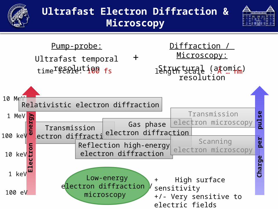
Ultrafast Electron Diffraction & Microscopy
Diffraction / Microscopy:
Structural (atomic) resolution
+time scale: 100 fs length scale : Å … nm
Pump-probe:
Ultrafast temporal resolution
Transmissionelectron diffraction
100 eV
1 keV
100 keV
10 keV
1 MeV
10 MeV
Gas phaseelectron diffraction
Relativistic electron diffraction
Reflection high-energyelectron diffraction
Scanningelectron microscopy
Transmissionelectron microscopy
Low-energyelectron diffraction /
microscopy
Ch
arg
e p
er
pu
lse
Ele
ctr
on
en
erg
y
+ High surface sensitivity+/- Very sensitive to electric fields+ Little sample damage

Major Challenge at Low Energies:Electron Pulse Duration
Nanotips as electron gun !
Delivering < 100-fs electron pulses at sub-kV energies is a big challenge !
Space charge
Vacuum dispersion
First time-resolved LEED: Karrer, Osterwalder et al., Rev. Sci. Instrum., 72 , 4404 (2001)4
Time-resolved experiments:
- Short propagation time → Compact design
- Single / few electron pulses at high rep-rate

Electron Pulse Duration: Simulations
5Paarmann et al., J. Appl. Phys. 112, 113109 (2012)
path length difference
dispersion
sample
tip
0.90
0
Utip = -200 Vd = 100 mmE0 = 0.5 eV

Beam Collimation for Diffraction:‚Lens Behind the Tip‘
6
U ≤ -100 V U > -100 V
Utip = -100 V
• Collimation (Focussing) due to plate-capacitor-like field lines
• Typically < 5 mm spot size on the sample• suppression of DC field enhancement + current• Disadvantage: dispersive pulse broadening
enhanced
Paarmann et al., J. Appl. Phys. 112, 113109 (2012)
Macrolens
Microlens
Lüneburg et al., Appl. Phys. Lett. 103 , 213506 (2013)
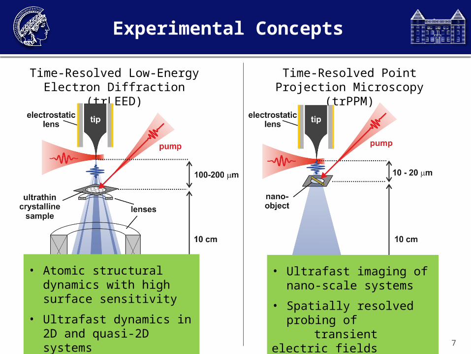
Experimental Concepts
7
Time-Resolved Low-EnergyElectron Diffraction (trLEED)
Time-Resolved Point Projection Microscopy (trPPM)
• Atomic structural dynamics with high surface sensitivity
• Ultrafast dynamics in 2D and quasi-2D systems
• Ultrafast imaging of nano-scale systems
• Spatially resolved probing of
transient electric fields

Experimental Setup
8
Ti:Sa oscillator80 MHz, 2 nJ, 5 fs
Cavity dumped Ti:Sa1 MHz, 30 nJ, 16 fs
Regenerative Ti:Sa amplifier
200 kHz, few mJ, 50 fs
100 nm 0.18
e-/pulse

Point Projection Imaging with fs-Electron Pulses
60 nm gold nanowires on quantifoil (2 μm holes)
Laser-triggered emissionDC field emission
Electron energy 100V
Tip-sample distance
25 μm
Integration time 1 s
Laser power 10 mW
Electron energy 150 V
Tip-sample distance
25 μm
Integration time 0.5 s

Transmission LEED of single-layer graphene
Unpublished data …

Space Charge Dynamics
• Generate space charge from a metal surface/edge and detect deflection of the probe electron beam
• Pt pinhole • Cu TEM grid edge
Laser
Coherent RegA
200 kHz, 50 fs
Pump
Power 31 mW
Fluence 50 mJ/cm2
Probe
Power 1.3 mW
Tip-sample distance 300 μm
Electron energy 261 eV
Lens bias -702 V
Space Charge Dynamics
Unpublished data …

Space charge dynamics
Unpublished data …

Transient Electric Fields at Photoexcited Semiconductor Nanowires
• time-resolved Point projection microscopy
• Semiconducting InP nanowires• Diameter: 30 nm, length: 1.5 μm
• Placed on quantifoil substrate
Hjort et al., ACS Nano 6, 9679 (2012)
Laser
Cavity dumped
1 MHz, 16 fs
Pump
Power 660 μW
Fluence 300 μJ/cm2
Probe
Power 1.4 mW
Tip-sample distance ~ 20 μm
Electron energy 70 eV
Lens bias -345 V

Nanowire Local Field Dynamics
Unpublished data …

Nanowire Local Field Dynamics
Unpublished data …

Outlook: „Divergent Beam LEED“
Unpublished data …

• Extremely compact, versatile machine for time-resolved low-energy electron diffraction and microscopy
• Large scattering cross section of low energy electrons• Best suited for low-dimensional systems• High sensitivity to local electric fields
• First observation of real-space local field dynamics at semiconductor nanowires
• Resolution in microscopy mode: < 200 fs, ~ 30 nm• Resolution in diffraction mode: < 2 ps, < 0.02 Å-1
Summary
Thanks for your attention!