max10 adc data capture lab - intellab 5. max10 adc data capture version 15.0 203 5.1 getting started...
TRANSCRIPT
Max10 ADC Data Capture LabFor the MAX® 10 DECA FPGA Evaluation Kit
TABLE OF CONTENTSLAB 5. MAX10 ADC DATA CAPTURE ............................................................................................................. 202
5.1 Getting Started ........................................................................................................................................ 2035.1.1 Prepare the analog Signal Source .................................................................................................. 203
5.2 ADC Core overview................................................................................................................................. 2035.3 Create a Simple ADC system; no Nios required..................................................................................... 205
5.3.1 Open the Quartus Project ............................................................................................................... 2055.3.2 Build the Qsys system .................................................................................................................... 2065.3.3 Complete the Qsys system ............................................................................................................. 2135.3.4 Verify your system........................................................................................................................... 2135.3.5 Generate the Qsys System............................................................................................................. 2145.3.6 Compile the design in Quartus........................................................................................................ 2165.3.7 Connect the Hardware .................................................................................................................... 2165.3.8 Test the Hardware .......................................................................................................................... 2175.3.9 Verify operation using the ADC Toolkit ........................................................................................... 2195.3.10 LED Volume Meter design .............................................................................................................. 2235.3.11 Debug the design using Signal Tap II ............................................................................................. 223
5.4 Create a software acquisition system, using Nios .................................................................................. 2265.4.1 Open the ADC Nios Lab project...................................................................................................... 2275.4.2 Modify the Qsys system.................................................................................................................. 2275.4.3 Compile the project in Quartus ....................................................................................................... 2305.4.4 Configure the FPGA........................................................................................................................ 2305.4.5 Create the Nios software application .............................................................................................. 2305.4.6 Configure the target hardware ........................................................................................................ 2355.4.7 Debug the application ..................................................................................................................... 2365.4.8 Other [possibly] helpful information................................................................................................. 239
Version 15.0 6/07/2015
LAB 5. MAX10 ADC Data Capture
202 Max10 DECA Workshop Manual
LAB 5. MAX10 ADC DATA CAPTUREOverview: The purpose of this lab is to learn about the basic architecture and configuration options for the MAX
10 ADC.
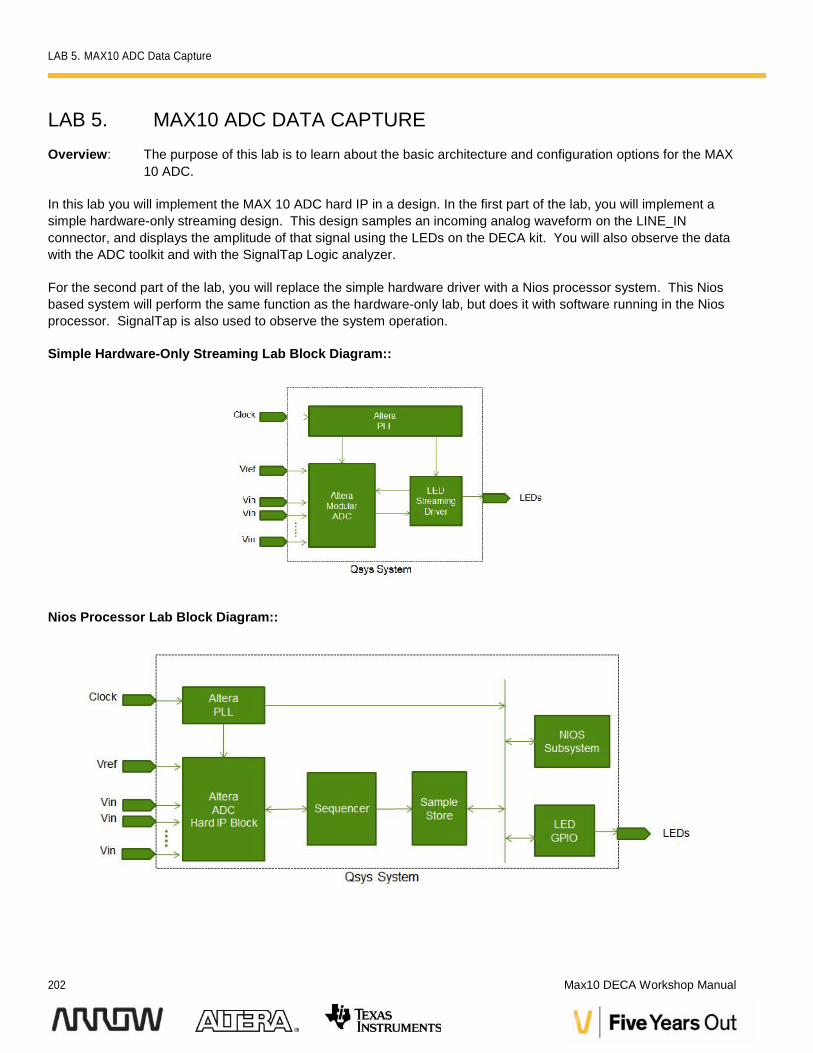
In this lab you will implement the MAX 10 ADC hard IP in a design. In the first part of the lab, you will implement asimple hardware-only streaming design. This design samples an incoming analog waveform on the LINE_INconnector, and displays the amplitude of that signal using the LEDs on the DECA kit. You will also observe the datawith the ADC toolkit and with the SignalTap Logic analyzer.
For the second part of the lab, you will replace the simple hardware driver with a Nios processor system. This Niosbased system will perform the same function as the hardware-only lab, but does it with software running in the Niosprocessor. SignalTap is also used to observe the system operation.
Simple Hardware-Only Streaming Lab Block Diagram::
Nios Processor Lab Block Diagram::
LAB 5. MAX10 ADC Data Capture
Version 15.0 203
5.1 Getting StartedOverview: The first objective is to ensure that you have all of the necessary hardware items and software installed
so that the lab can be completed successfully.
Below is a list of items required to complete this lab:
Arrow DECA Evaluation Kit
USB cable
2.5mm Audio cable
Analog Signal Generator (Smart phone with Waveform App will work)
Lab files
Quartus II 15.0 Design Software
Personal computer or laptop running Windows 7 with at least an Intel i3 core (or equivalent),4 GB of RAM, and 12 GB of free hard disk space
A desire to learn
If you are missing one of these items, please your instructor know. Instructions for how to download Quartus can befound in the Appendix.
5.1.1 Prepare the analog Signal SourceThis lab requires an analog signal source. A smart phone with a Waveform generator app will work, although youshould not expect good results for the linearity measurement portion of the Lab. If you are using a smart phone forthis lab, please prepare it now by downloading and installing an appropriate application. For best results, choose anapp that can generate sinewaves, and permits manually entering the desired frequency. Waveform Generator Liteand Frequency Sound Generator are two possible options.
If your laptop has a headphone jack, you can use it to generate a sine wave from: http://onlinetonegenerator.com/
5.2 ADC Core overviewAltera supports four configuration variants of the ADC core:
LAB 5. MAX10 ADC Data Capture
204 Max10 DECA Workshop Manual
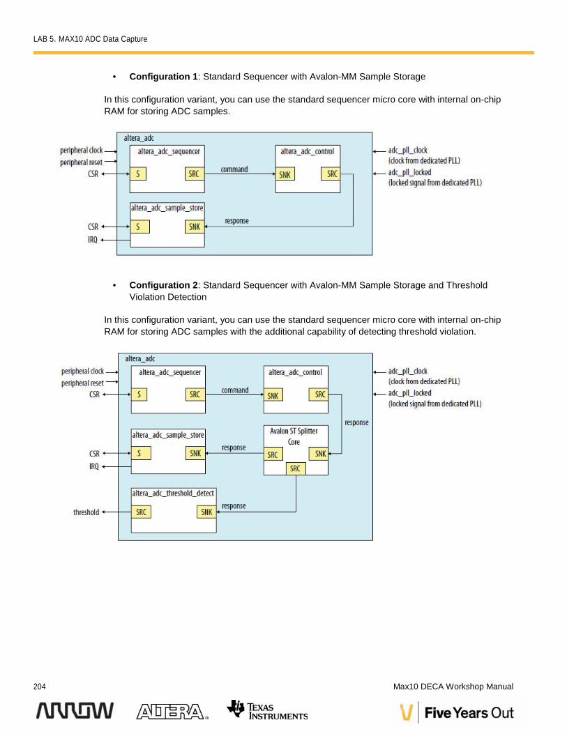
Configuration 1: Standard Sequencer with Avalon-MM Sample Storage
In this configuration variant, you can use the standard sequencer micro core with internal on-chipRAM for storing ADC samples.
Configuration 2: Standard Sequencer with Avalon-MM Sample Storage and ThresholdViolation Detection
In this configuration variant, you can use the standard sequencer micro core with internal on-chipRAM for storing ADC samples with the additional capability of detecting threshold violation.
LAB 5. MAX10 ADC Data Capture
Version 15.0 205
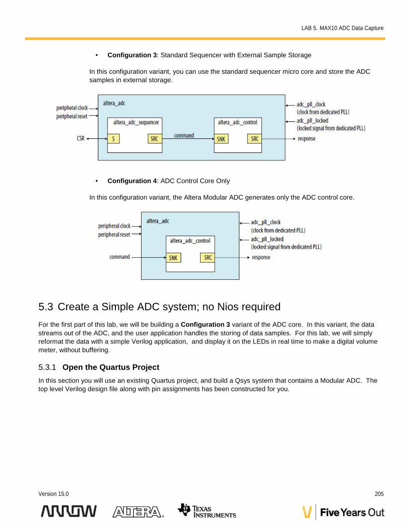
Configuration 3: Standard Sequencer with External Sample Storage
In this configuration variant, you can use the standard sequencer micro core and store the ADCsamples in external storage.
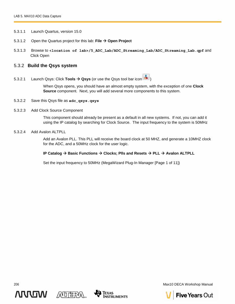
Configuration 4: ADC Control Core Only
In this configuration variant, the Altera Modular ADC generates only the ADC control core.
5.3 Create a Simple ADC system; no Nios requiredFor the first part of this lab, we will be building a Configuration 3 variant of the ADC core. In this variant, the datastreams out of the ADC, and the user application handles the storing of data samples. For this lab, we will simplyreformat the data with a simple Verilog application, and display it on the LEDs in real time to make a digital volumemeter, without buffering.
5.3.1 Open the Quartus ProjectIn this section you will use an existing Quartus project, and build a Qsys system that contains a Modular ADC. Thetop level Verilog design file along with pin assignments has been constructed for you.
LAB 5. MAX10 ADC Data Capture
206 Max10 DECA Workshop Manual
5.3.1.1 Launch Quartus, version 15.0
5.3.1.2 Open the Quartus project for this lab: File Open Project
5.3.1.3 Browse to <location of lab>/5_ADC_Lab/ADC_Streaming_Lab/ADC_Streaming_Lab.qpf andClick Open
5.3.2 Build the Qsys system
5.3.2.1 Launch Qsys: Click Tools Qsys (or use the Qsys tool bar icon )
When Qsys opens, you should have an almost empty system, with the exception of one ClockSource component. Next, you will add several more components to this system.
5.3.2.2 Save this Qsys file as adc_qsys.qsys
5.3.2.3 Add Clock Source Component
This component should already be present as a default in all new systems. If not, you can add itusing the IP catalog by searching for Clock Source. The input frequency to the system is 50MHz
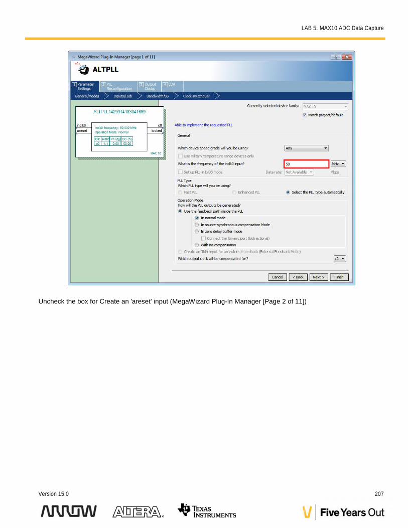
5.3.2.4 Add Avalon ALTPLL
Add an Avalon PLL. This PLL will receive the board clock at 50 MHZ, and generate a 10MHZ clockfor the ADC, and a 50MHz clock for the user logic.
IP Catalog Basic Functions Clocks; Plls and Resets PLL Avalon ALTPLL
Set the input frequency to 50MHz (MegaWizard Plug-In Manager [Page 1 of 11])
LAB 5. MAX10 ADC Data Capture
Version 15.0 207
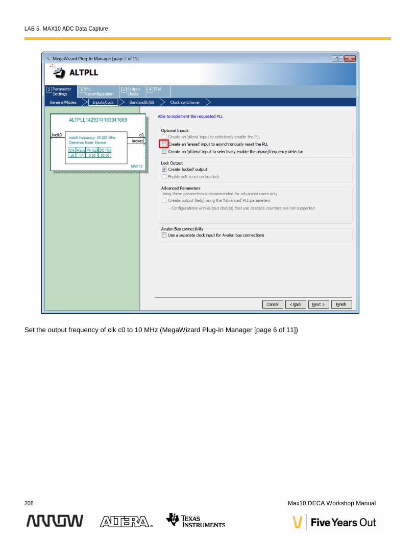
Uncheck the box for Create an 'areset' input (MegaWizard Plug-In Manager [Page 2 of 11])
LAB 5. MAX10 ADC Data Capture
208 Max10 DECA Workshop Manual
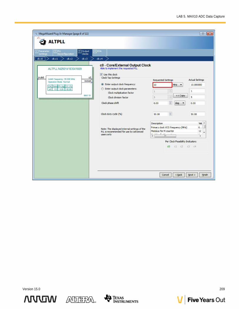
Set the output frequency of clk c0 to 10 MHz (MegaWizard Plug-In Manager [page 6 of 11])
LAB 5. MAX10 ADC Data Capture
Version 15.0 209
LAB 5. MAX10 ADC Data Capture
210 Max10 DECA Workshop Manual
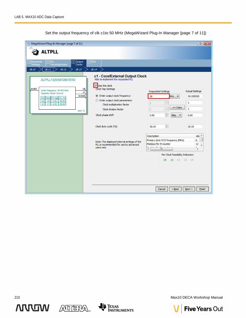
Set the output frequency of clk c1to 50 MHz (MegaWizard Plug-In Manager [page 7 of 11])
LAB 5. MAX10 ADC Data Capture
Version 15.0 211
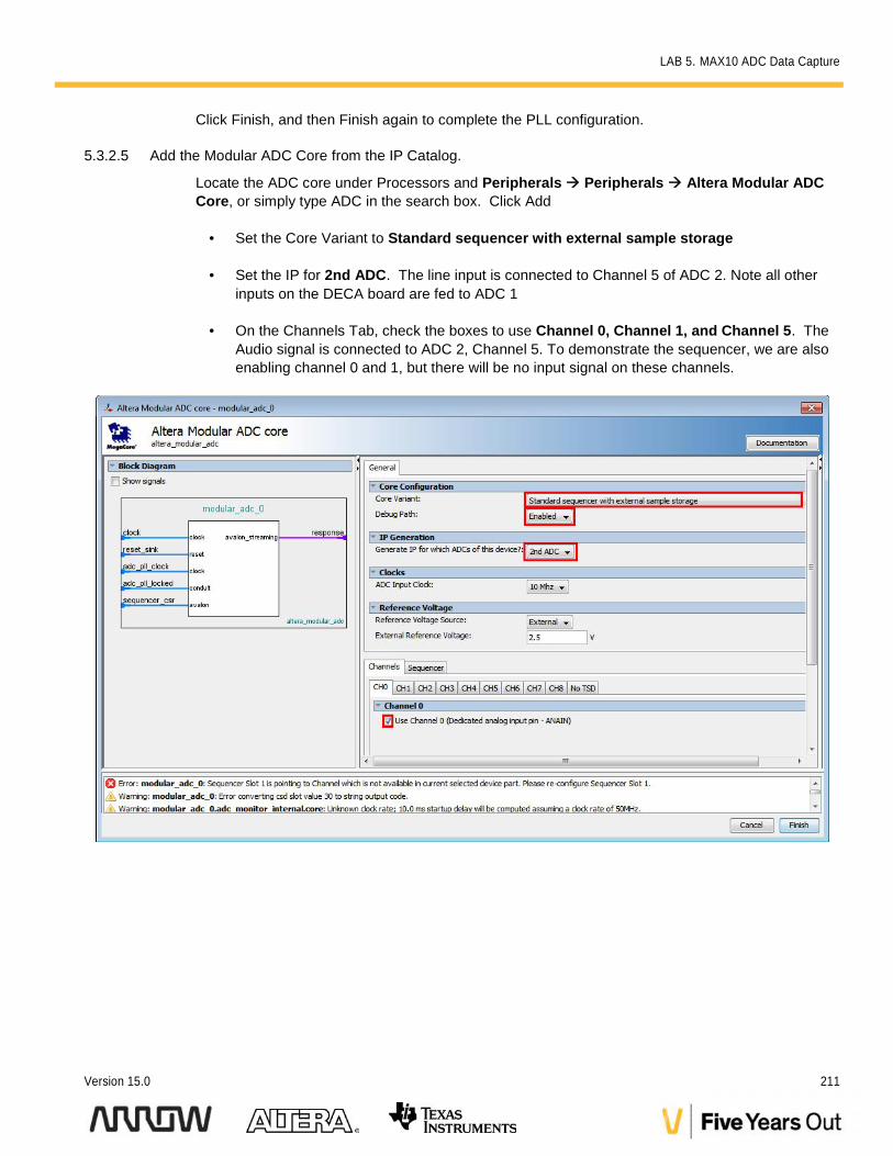
Click Finish, and then Finish again to complete the PLL configuration.
5.3.2.5 Add the Modular ADC Core from the IP Catalog.
Locate the ADC core under Processors and Peripherals Peripherals Altera Modular ADCCore, or simply type ADC in the search box. Click Add
Set the Core Variant to Standard sequencer with external sample storage
Set the IP for 2nd ADC. The line input is connected to Channel 5 of ADC 2. Note all otherinputs on the DECA board are fed to ADC 1
On the Channels Tab, check the boxes to use Channel 0, Channel 1, and Channel 5. TheAudio signal is connected to ADC 2, Channel 5. To demonstrate the sequencer, we are alsoenabling channel 0 and 1, but there will be no input signal on these channels.
LAB 5. MAX10 ADC Data Capture
212 Max10 DECA Workshop Manual
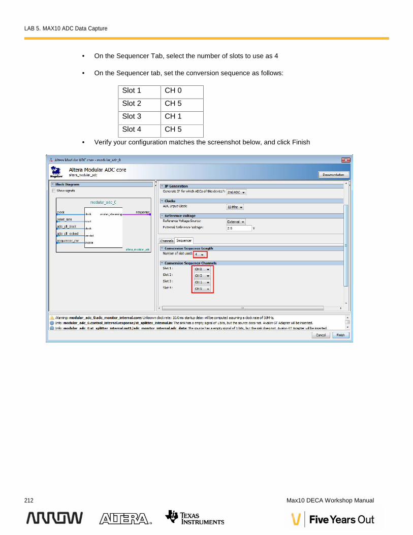
On the Sequencer Tab, select the number of slots to use as 4
On the Sequencer tab, set the conversion sequence as follows:
Slot 1 CH 0
Slot 2 CH 5
Slot 3 CH 1
Slot 4 CH 5
Verify your configuration matches the screenshot below, and click Finish
LAB 5. MAX10 ADC Data Capture
Version 15.0 213
5.3.2.6 Add the LED_Streaming_Driver.
This is a custom component that is be located in the DECA Labs folder of the IP Catalog. There areno configurable options for this component, so just click Finish
If you want to inspect the verilog code for this component, it is located in the IP directory. Insummary, this component has three interfaces:
An Avalon memory mapped master for writing commands to the ADC sequencer control andstatus register. After coming out of reset, the LED Driver performs a single write to the ADCsequencer to put the ADC in continuous acquisition run mode.
An Avalon streaming sink to receive the data from the ADC "response" streaming source. TheLED driver receives the data and channel information, so it can ignore other channels, if theyare enabled. The Audio LINE_IN signal is on channel 5.
An exported conduit that drives the board LEDs. The value output is based on the analoglevel received from the ADC
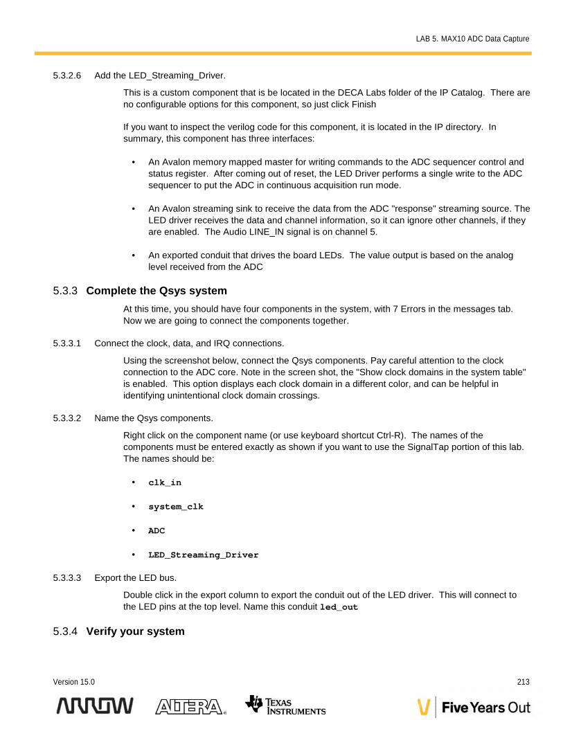
5.3.3 Complete the Qsys systemAt this time, you should have four components in the system, with 7 Errors in the messages tab.Now we are going to connect the components together.
5.3.3.1 Connect the clock, data, and IRQ connections.
Using the screenshot below, connect the Qsys components. Pay careful attention to the clockconnection to the ADC core. Note in the screen shot, the "Show clock domains in the system table"is enabled. This option displays each clock domain in a different color, and can be helpful inidentifying unintentional clock domain crossings.
5.3.3.2 Name the Qsys components.
Right click on the component name (or use keyboard shortcut Ctrl-R). The names of thecomponents must be entered exactly as shown if you want to use the SignalTap portion of this lab.The names should be:
clk_in
system_clk
ADC
LED_Streaming_Driver
5.3.3.3 Export the LED bus.
Double click in the export column to export the conduit out of the LED driver. This will connect tothe LED pins at the top level. Name this conduit led_out
5.3.4 Verify your system
LAB 5. MAX10 ADC Data Capture
214 Max10 DECA Workshop Manual
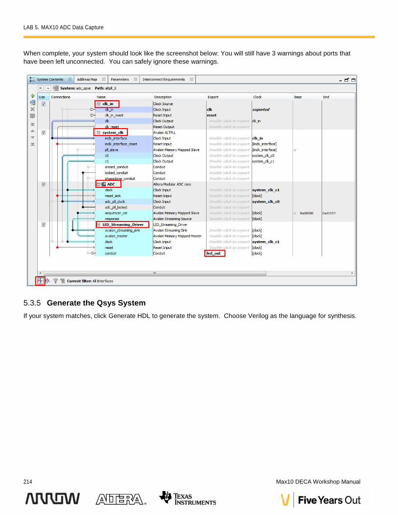
When complete, your system should look like the screenshot below: You will still have 3 warnings about ports thathave been left unconnected. You can safely ignore these warnings.
5.3.5 Generate the Qsys SystemIf your system matches, click Generate HDL to generate the system. Choose Verilog as the language for synthesis.
LAB 5. MAX10 ADC Data Capture
Version 15.0 215
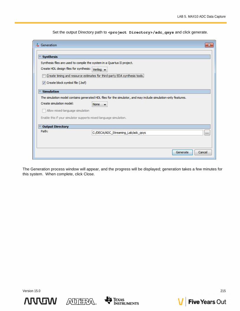
Set the output Directory path to <project Directory>/adc_qsys and click generate.
The Generation process window will appear, and the progress will be displayed; generation takes a few minutes forthis system. When complete, click Close.
LAB 5. MAX10 ADC Data Capture
216 Max10 DECA Workshop Manual
5.3.6 Compile the design in Quartus
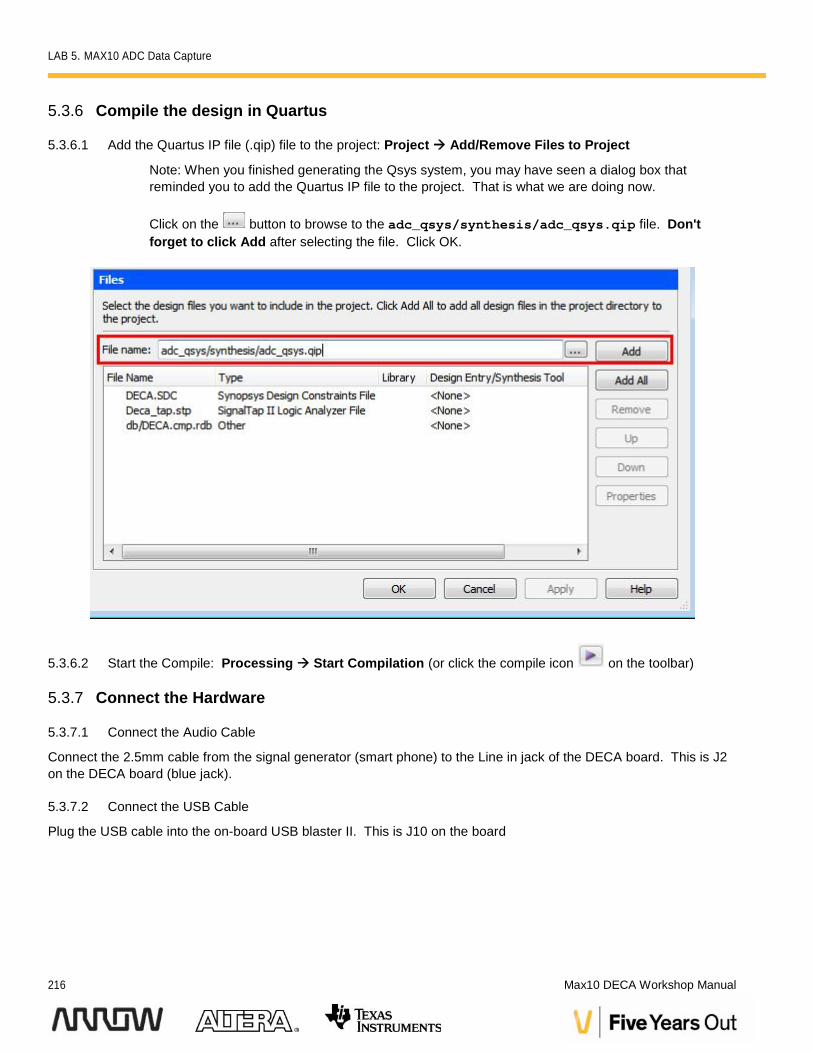
5.3.6.1 Add the Quartus IP file (.qip) file to the project: Project Add/Remove Files to Project
Note: When you finished generating the Qsys system, you may have seen a dialog box thatreminded you to add the Quartus IP file to the project. That is what we are doing now.
Click on the button to browse to the adc_qsys/synthesis/adc_qsys.qip file. Don'tforget to click Add after selecting the file. Click OK.
5.3.6.2 Start the Compile: Processing Start Compilation (or click the compile icon on the toolbar)
5.3.7 Connect the Hardware
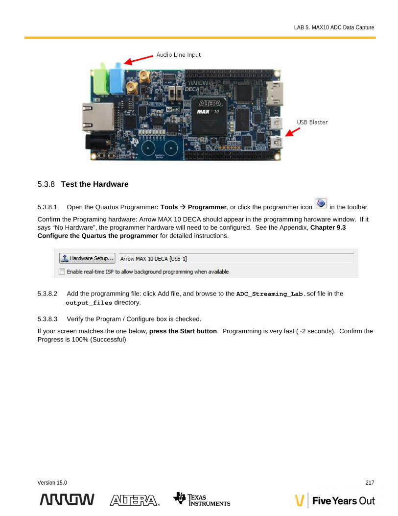
5.3.7.1 Connect the Audio Cable
Connect the 2.5mm cable from the signal generator (smart phone) to the Line in jack of the DECA board. This is J2on the DECA board (blue jack).
5.3.7.2 Connect the USB Cable
Plug the USB cable into the on-board USB blaster II. This is J10 on the board
LAB 5. MAX10 ADC Data Capture
Version 15.0 217
5.3.8 Test the Hardware
5.3.8.1 Open the Quartus Programmer: Tools Programmer, or click the programmer icon in the toolbar
Confirm the Programing hardware: Arrow MAX 10 DECA should appear in the programming hardware window. If itsays “No Hardware”, the programmer hardware will need to be configured. See the Appendix, Chapter 9.3Configure the Quartus the programmer for detailed instructions.
5.3.8.2 Add the programming file: click Add file, and browse to the ADC_Streaming_Lab.sof file in theoutput_files directory.
5.3.8.3 Verify the Program / Configure box is checked.
If your screen matches the one below, press the Start button. Programming is very fast (~2 seconds). Confirm theProgress is 100% (Successful)

LAB 5. MAX10 ADC Data Capture
218 Max10 DECA Workshop Manual
LAB 5. MAX10 ADC Data Capture
Version 15.0 219
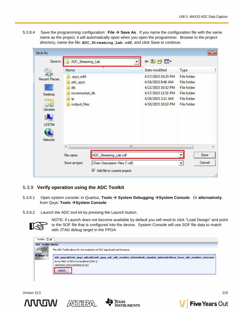
5.3.8.4 Save the programming configuration: File Save As. If you name the configuration file with the samename as the project, it will automatically open when you open the programmer. Browse to the projectdirectory, name the file: ADC_Streaming_Lab.cdf, and click Save to continue.
5.3.9 Verify operation using the ADC Toolkit
5.3.9.1 Open system console: in Quartus, Tools System DebuggingSystem Console. Or alternatively,from Qsys: ToolsSystem Console
5.3.9.2 Launch the ADC tool kit by pressing the Launch button.
NOTE: if Launch does not become available by default you will need to click “Load Design” and pointto the SOF file that is configured into the device. System Console will use SOF file data to matchwith JTAG debug target in the FPGA
LAB 5. MAX10 ADC Data Capture
220 Max10 DECA Workshop Manual
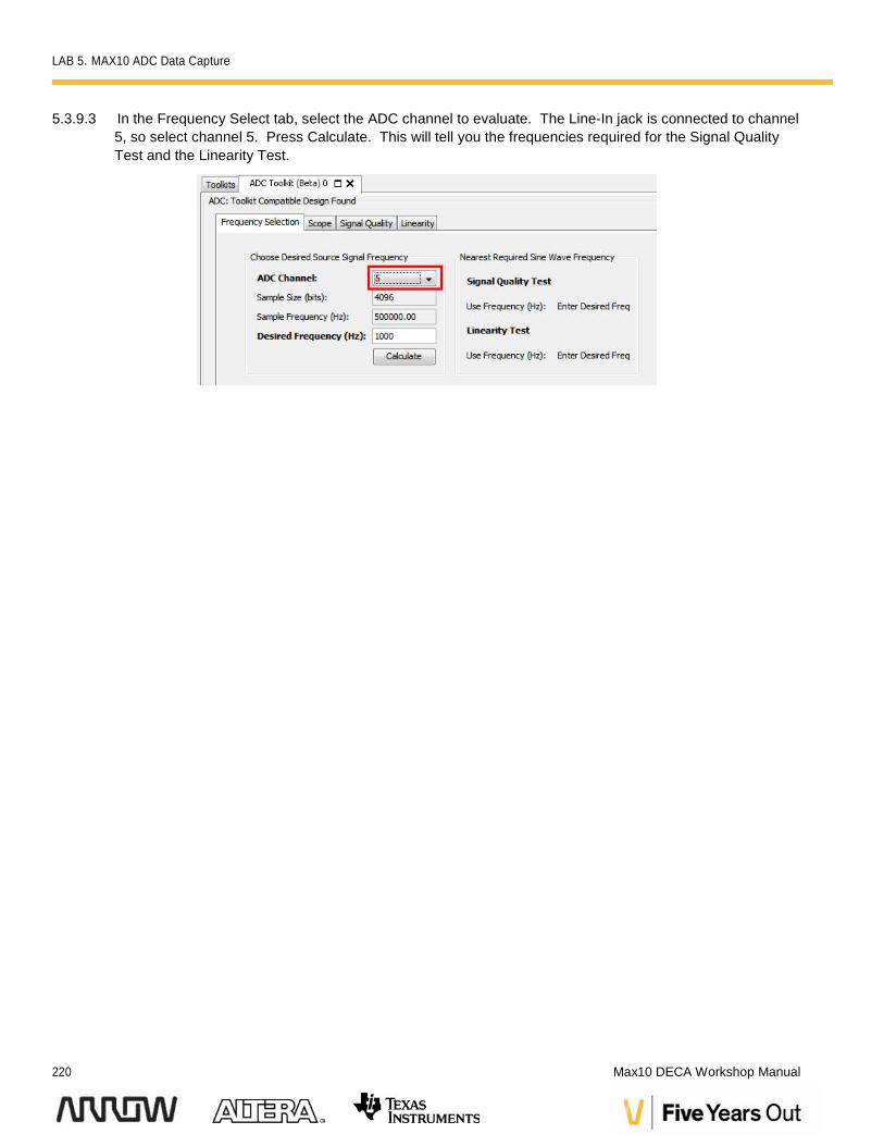
5.3.9.3 In the Frequency Select tab, select the ADC channel to evaluate. The Line-In jack is connected to channel5, so select channel 5. Press Calculate. This will tell you the frequencies required for the Signal QualityTest and the Linearity Test.
LAB 5. MAX10 ADC Data Capture
Version 15.0 221
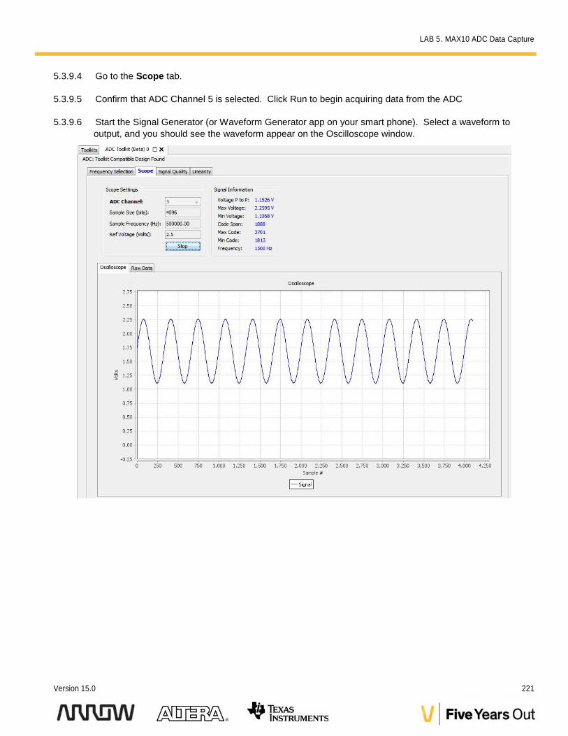
5.3.9.4 Go to the Scope tab.
5.3.9.5 Confirm that ADC Channel 5 is selected. Click Run to begin acquiring data from the ADC
5.3.9.6 Start the Signal Generator (or Waveform Generator app on your smart phone). Select a waveform tooutput, and you should see the waveform appear on the Oscilloscope window.
LAB 5. MAX10 ADC Data Capture
222 Max10 DECA Workshop Manual
5.3.9.7 Click Stop to move to the next section
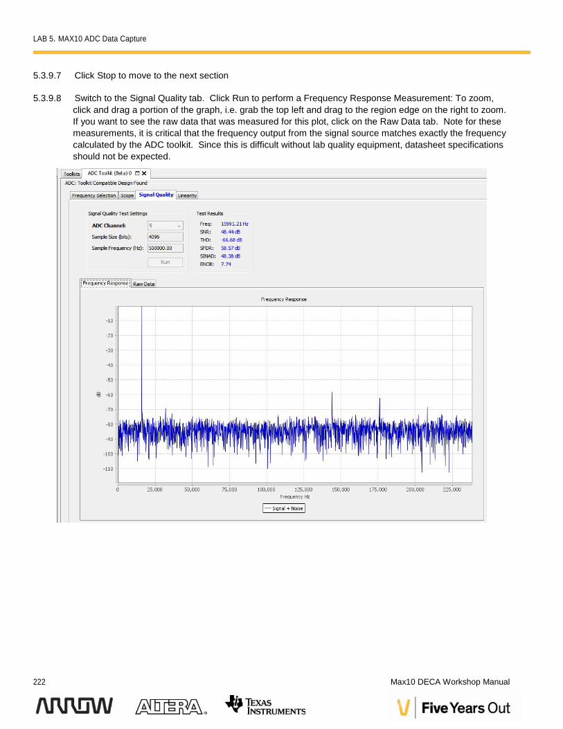
5.3.9.8 Switch to the Signal Quality tab. Click Run to perform a Frequency Response Measurement: To zoom,click and drag a portion of the graph, i.e. grab the top left and drag to the region edge on the right to zoom.If you want to see the raw data that was measured for this plot, click on the Raw Data tab. Note for thesemeasurements, it is critical that the frequency output from the signal source matches exactly the frequencycalculated by the ADC toolkit. Since this is difficult without lab quality equipment, datasheet specificationsshould not be expected.
LAB 5. MAX10 ADC Data Capture
Version 15.0 223
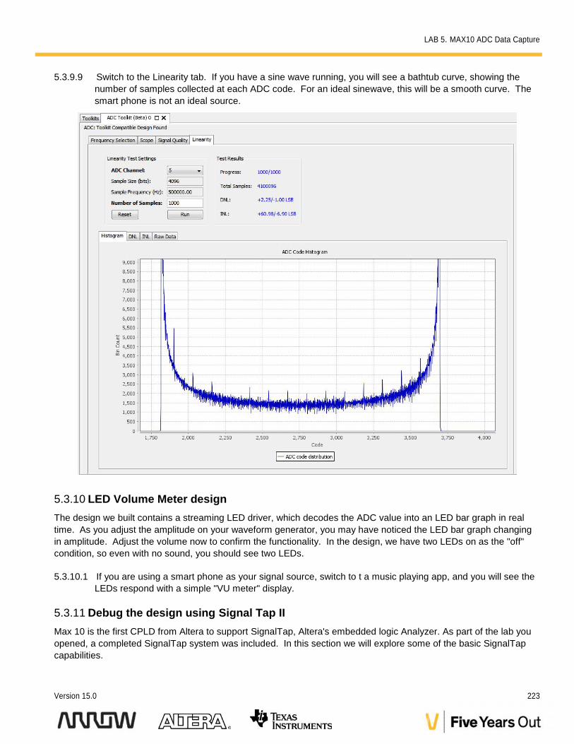
5.3.9.9 Switch to the Linearity tab. If you have a sine wave running, you will see a bathtub curve, showing thenumber of samples collected at each ADC code. For an ideal sinewave, this will be a smooth curve. Thesmart phone is not an ideal source.
5.3.10 LED Volume Meter designThe design we built contains a streaming LED driver, which decodes the ADC value into an LED bar graph in realtime. As you adjust the amplitude on your waveform generator, you may have noticed the LED bar graph changingin amplitude. Adjust the volume now to confirm the functionality. In the design, we have two LEDs on as the "off"condition, so even with no sound, you should see two LEDs.
5.3.10.1 If you are using a smart phone as your signal source, switch to t a music playing app, and you will see theLEDs respond with a simple "VU meter" display.
5.3.11 Debug the design using Signal Tap IIMax 10 is the first CPLD from Altera to support SignalTap, Altera's embedded logic Analyzer. As part of the lab youopened, a completed SignalTap system was included. In this section we will explore some of the basic SignalTapcapabilities.
LAB 5. MAX10 ADC Data Capture
224 Max10 DECA Workshop Manual
5.3.11.1 Open SignalTap: Tools SignalTap II Logic Analyzer
If you have already programmed the device, the system status should be "Ready to Acquire". If not, program thedevice using the Quartus programmer, or use the programmer built into SignalTap.
NOTE: In some cases, Quartus II Web-Edition will throw an error when launching SignalTap. Alterarequires that you enable the TalkBack feature in order to use the SignalTap II Logic Analyzer.
If so, follow these steps:
Go to the menu: Tools Options and select the Category: Internet Connectivity. In the right-handpane, click the TalkBack Options… button then check the Enable sending TalkBack data to Alteracheckbox.
Click OK twice to close both the Quartus II TalkBack dialog box as well as the Options dialog box.
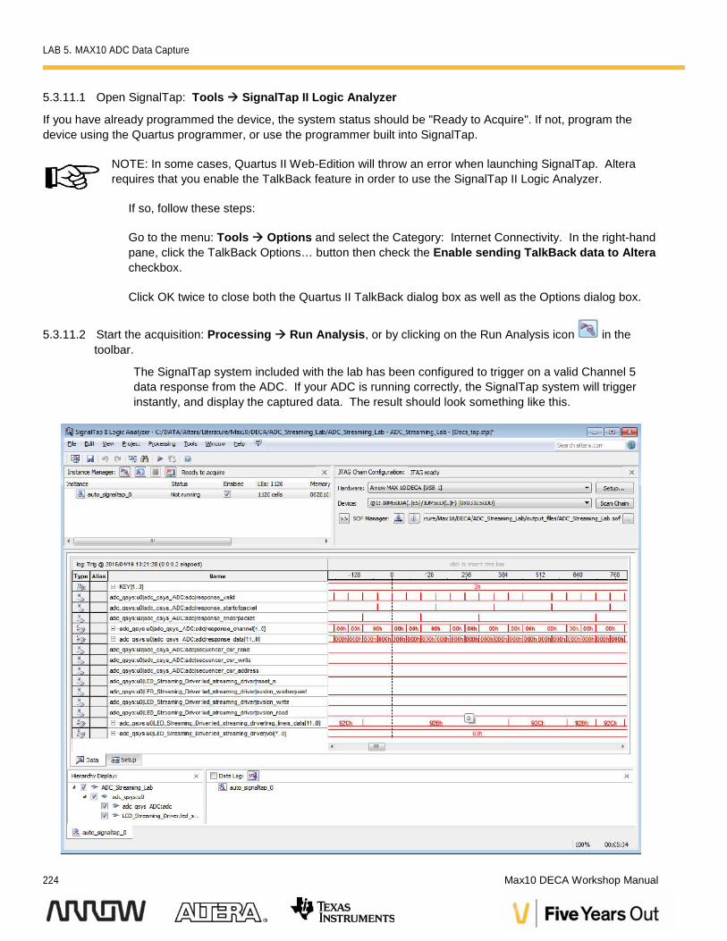
5.3.11.2 Start the acquisition: Processing Run Analysis, or by clicking on the Run Analysis icon in thetoolbar.
The SignalTap system included with the lab has been configured to trigger on a valid Channel 5data response from the ADC. If your ADC is running correctly, the SignalTap system will triggerinstantly, and display the captured data. The result should look something like this.
LAB 5. MAX10 ADC Data Capture
Version 15.0 225
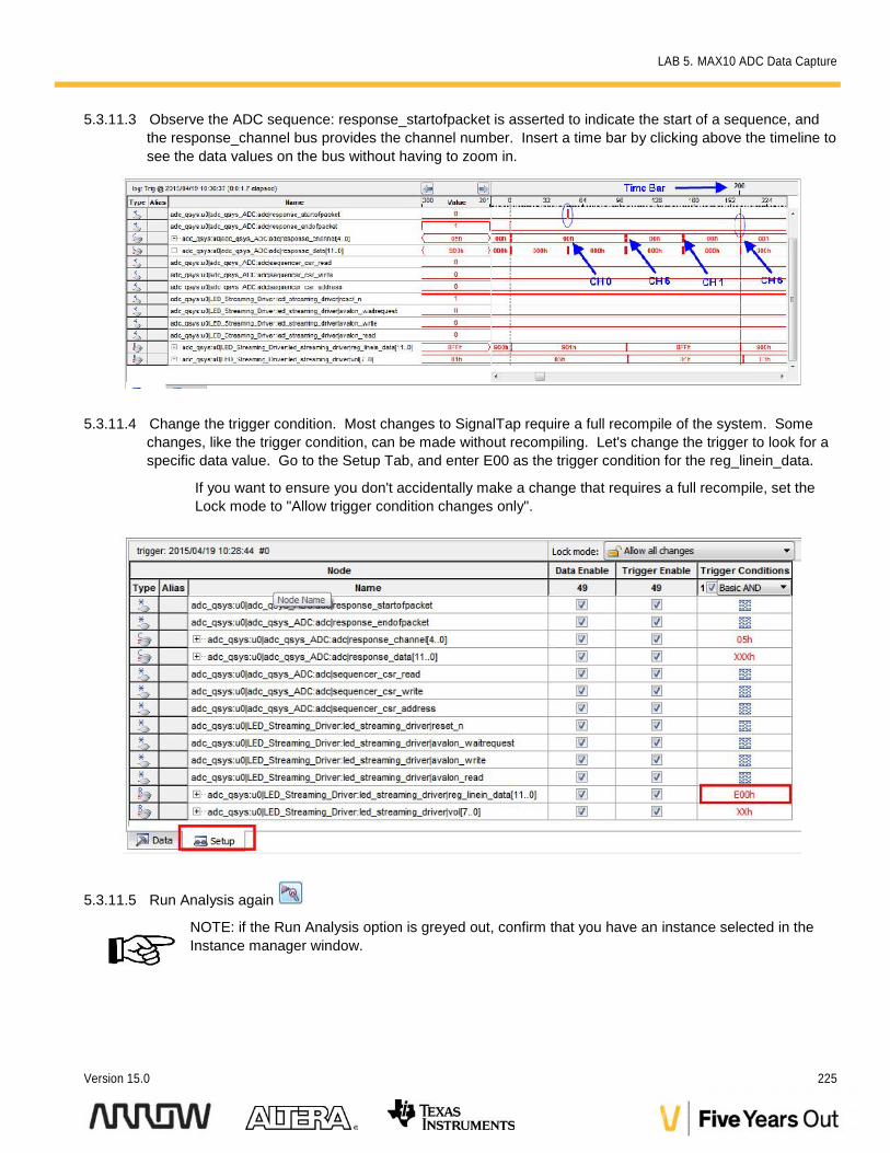
5.3.11.3 Observe the ADC sequence: response_startofpacket is asserted to indicate the start of a sequence, andthe response_channel bus provides the channel number. Insert a time bar by clicking above the timeline tosee the data values on the bus without having to zoom in.
5.3.11.4 Change the trigger condition. Most changes to SignalTap require a full recompile of the system. Somechanges, like the trigger condition, can be made without recompiling. Let's change the trigger to look for aspecific data value. Go to the Setup Tab, and enter E00 as the trigger condition for the reg_linein_data.
If you want to ensure you don't accidentally make a change that requires a full recompile, set theLock mode to "Allow trigger condition changes only".
5.3.11.5 Run Analysis again
NOTE: if the Run Analysis option is greyed out, confirm that you have an instance selected in theInstance manager window.
LAB 5. MAX10 ADC Data Capture
226 Max10 DECA Workshop Manual
This time, the system may not trigger immediately, depending on the input level from your signalsource. Turn the volume up, and the system should trigger. If not, try a lower trigger value, like900h
That completes this portion of the Lab.
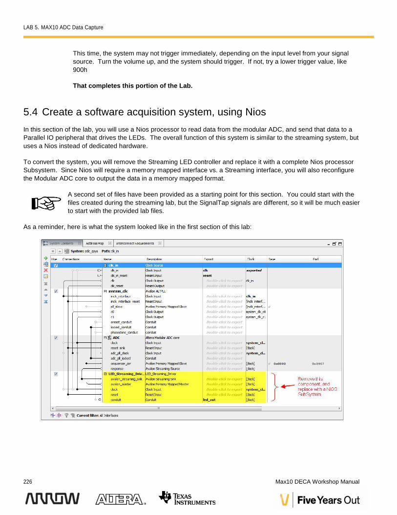
5.4 Create a software acquisition system, using NiosIn this section of the lab, you will use a Nios processor to read data from the modular ADC, and send that data to aParallel IO peripheral that drives the LEDs. The overall function of this system is similar to the streaming system, butuses a Nios instead of dedicated hardware.
To convert the system, you will remove the Streaming LED controller and replace it with a complete Nios processorSubsystem. Since Nios will require a memory mapped interface vs. a Streaming interface, you will also reconfigurethe Modular ADC core to output the data in a memory mapped format.
A second set of files have been provided as a starting point for this section. You could start with thefiles created during the streaming lab, but the SignalTap signals are different, so it will be much easierto start with the provided lab files.
As a reminder, here is what the system looked like in the first section of this lab:
LAB 5. MAX10 ADC Data Capture
Version 15.0 227
5.4.1 Open the ADC Nios Lab project
5.4.1.1 Close the Streaming Lab Project (if necessary), closing all open Quartus windows, including Qsys,SignalTap, programmer, etc.
5.4.1.2 Open the ADC Nios Lab Project: File Open Project and browse to <location of
lab>\workshop_labs\5_ADC_Lab\ADC_Nios_Lab\ADC_Nios_Lab.qpf. Click Open
5.4.2 Modify the Qsys system
5.4.2.1 Launch Qsys: Click Tools Qsys (or use the Qsys tool bar icon )
5.4.2.2 Open the Qsys system <project directory>\adc_qsys.qsys
5.4.2.3 Delete the LED_Streaming_Driver. Click on the module and press Delete (Or alternatively, right click,and select Delete)
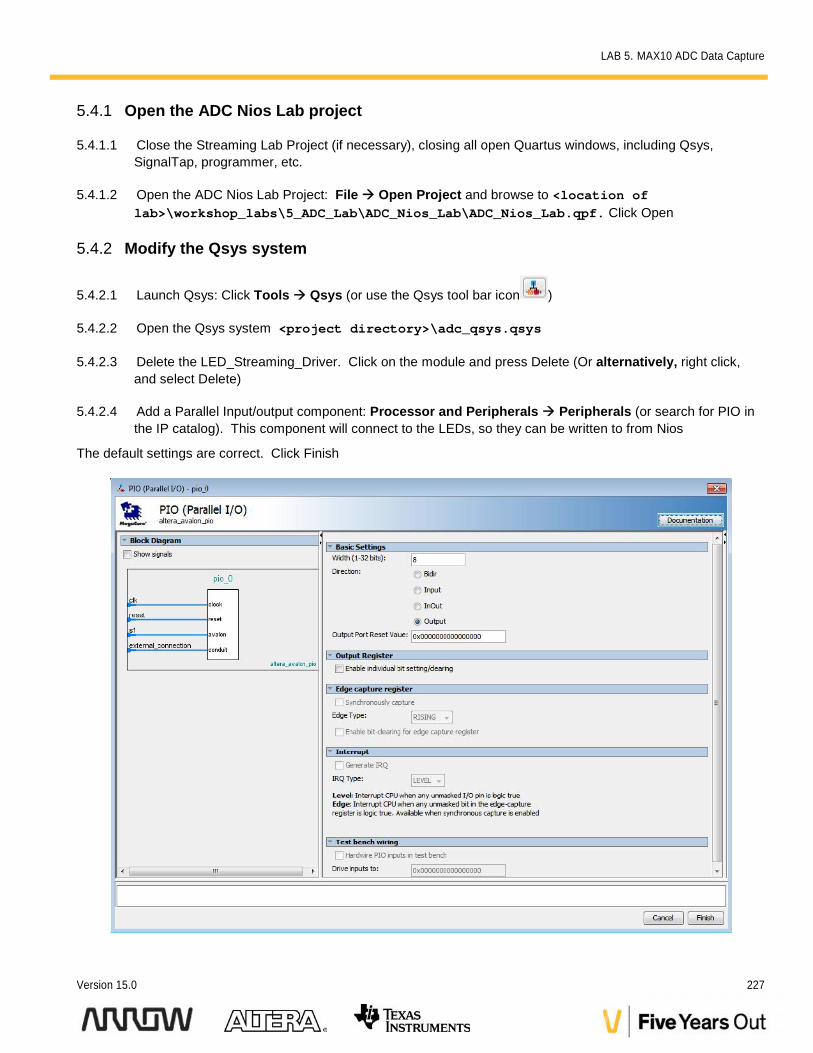
5.4.2.4 Add a Parallel Input/output component: Processor and Peripherals Peripherals (or search for PIO inthe IP catalog). This component will connect to the LEDs, so they can be written to from Nios
The default settings are correct. Click Finish
LAB 5. MAX10 ADC Data Capture
228 Max10 DECA Workshop Manual
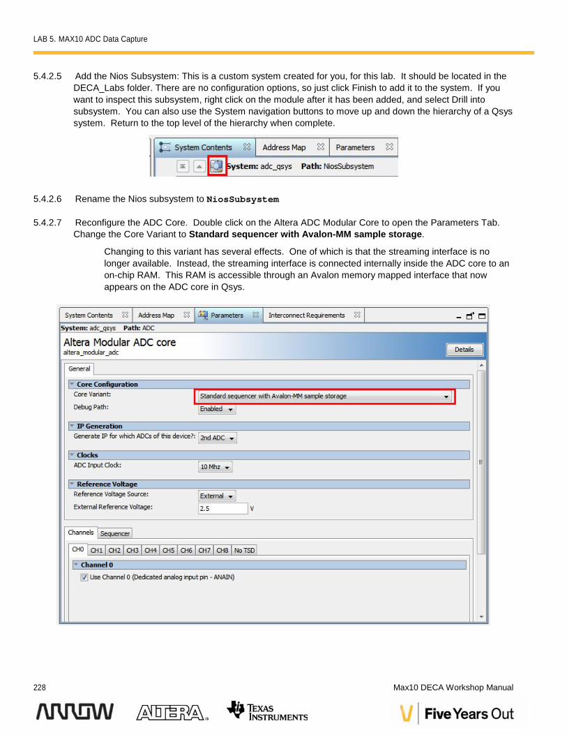
5.4.2.5 Add the Nios Subsystem: This is a custom system created for you, for this lab. It should be located in theDECA_Labs folder. There are no configuration options, so just click Finish to add it to the system. If youwant to inspect this subsystem, right click on the module after it has been added, and select Drill intosubsystem. You can also use the System navigation buttons to move up and down the hierarchy of a Qsyssystem. Return to the top level of the hierarchy when complete.
5.4.2.6 Rename the Nios subsystem to NiosSubsystem
5.4.2.7 Reconfigure the ADC Core. Double click on the Altera ADC Modular Core to open the Parameters Tab.Change the Core Variant to Standard sequencer with Avalon-MM sample storage.
Changing to this variant has several effects. One of which is that the streaming interface is nolonger available. Instead, the streaming interface is connected internally inside the ADC core to anon-chip RAM. This RAM is accessible through an Avalon memory mapped interface that nowappears on the ADC core in Qsys.
LAB 5. MAX10 ADC Data Capture
Version 15.0 229
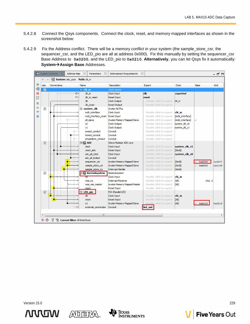
5.4.2.8 Connect the Qsys components. Connect the clock, reset, and memory mapped interfaces as shown in thescreenshot below:
5.4.2.9 Fix the Address conflict. There will be a memory conflict in your system (the sample_store_csr, thesequencer_csr, and the LED_pio are all at address 0x000). Fix this manually by setting the sequencer_csrBase Address to 0x0200, and the LED_pio to 0x0210. Alternatively, you can let Qsys fix it automatically:SystemAssign Base Addresses.
LAB 5. MAX10 ADC Data Capture
230 Max10 DECA Workshop Manual
5.4.2.10 Generate the system. You should have 3 warnings; these can be ignored. Click Generate HDL to openthe Generate Dialog box, and click Generate to begin the generation process.
5.4.2.11 If there are no errors, click Close to close the Qsys Generation status dialog box.
5.4.2.12 Close Qsys and return to Quartus. If you get a message reminding you to add the qip, you can ignore thismessage, as the qip was added for you in this project.
5.4.3 Compile the project in Quartus
5.4.3.1 Start the Compile: Processing Start Compilation (or click the compile icon on the toolbar)
Confirm the compile completed successfully.
5.4.4 Configure the FPGA
5.4.4.1 Open the Quartus II Programmer via Tools Programmer
5.4.4.2 The Programmer window will open with a predefined Chain-Description File (ADC_Nios_Lab.cdf) thatspecifies the programming file output_files/ADC_Nios_Lab.sof
5.4.4.3 Click Start to begin configure the FPGA.
5.4.5 Create the Nios software application
5.4.5.1 Open Eclipse: From Quartus, Tools Nios II Software Build Tools for Eclipse
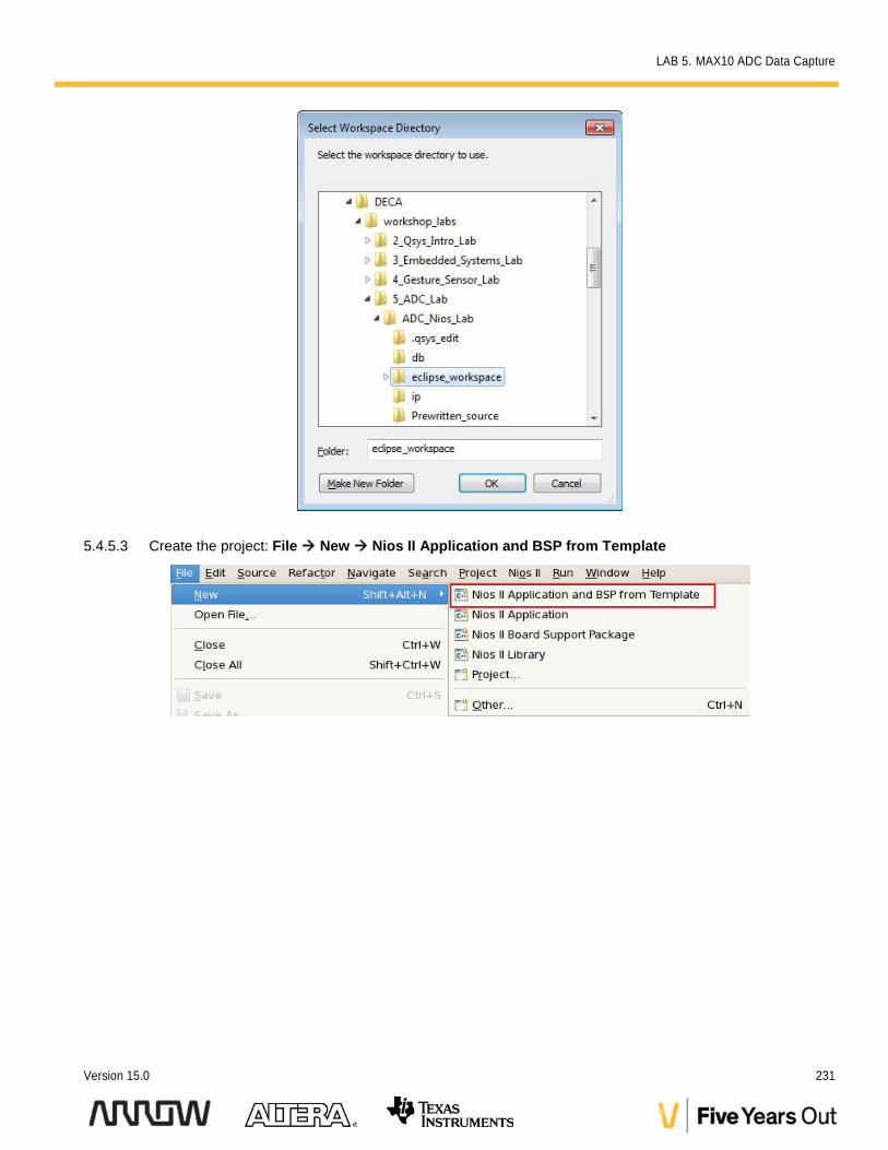
5.4.5.2 Select a workspace: It is recommended that you create a workspace named eclipse_workspace in thesame directory as the Quartus project files. Browse to the project folder and click Make New Folder.Rename the folder to eclipse_workspace . Click OK to continue
LAB 5. MAX10 ADC Data Capture
Version 15.0 231
5.4.5.3 Create the project: File New Nios II Application and BSP from Template
LAB 5. MAX10 ADC Data Capture
232 Max10 DECA Workshop Manual
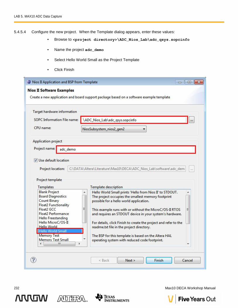
5.4.5.4 Configure the new project. When the Template dialog appears, enter these values:
Browse to <project directory>\ADC_Nios_Lab\adc_qsys.sopcinfo
Name the project adc_demo
Select Hello World Small as the Project Template
Click Finish
LAB 5. MAX10 ADC Data Capture
Version 15.0 233
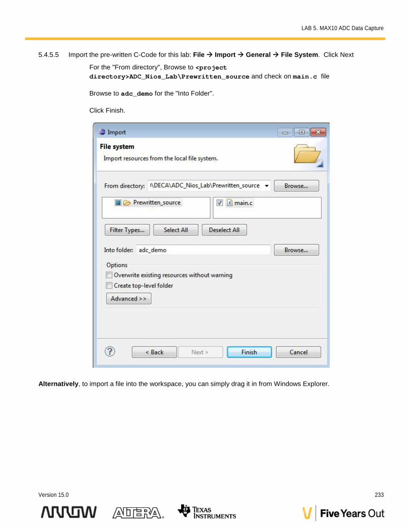
5.4.5.5 Import the pre-written C-Code for this lab: File Import General File System. Click Next
For the "From directory", Browse to <project
directory>ADC_Nios_Lab\Prewritten_source and check on main.c file
Browse to adc_demo for the "Into Folder".
Click Finish.
Alternatively, to import a file into the workspace, you can simply drag it in from Windows Explorer.
LAB 5. MAX10 ADC Data Capture
234 Max10 DECA Workshop Manual
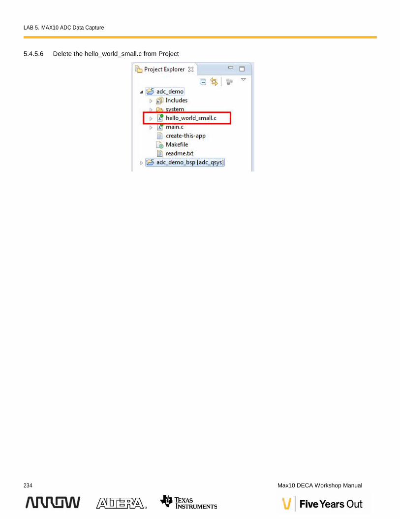
5.4.5.6 Delete the hello_world_small.c from Project
LAB 5. MAX10 ADC Data Capture
Version 15.0 235
5.4.5.7 Build the project : Project Build All (or click the Build All icon on the toolbar
5.4.6 Configure the target hardware
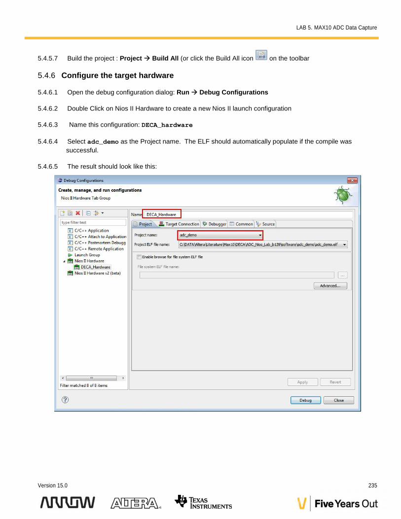
5.4.6.1 Open the debug configuration dialog: Run Debug Configurations
5.4.6.2 Double Click on Nios II Hardware to create a new Nios II launch configuration
5.4.6.3 Name this configuration: DECA_hardware
5.4.6.4 Select adc_demo as the Project name. The ELF should automatically populate if the compile wassuccessful.
5.4.6.5 The result should look like this:
LAB 5. MAX10 ADC Data Capture
236 Max10 DECA Workshop Manual
5.4.6.6 Click Debug to begin debugging the application.
5.4.7 Debug the applicationWhen you begin the debug session, the debugger downloads the code to the on-chip RAM, and begins executing thecode. A breakpoint is automatically set at the entry point to main(), so the processor should be paused, waiting foryou to resume.
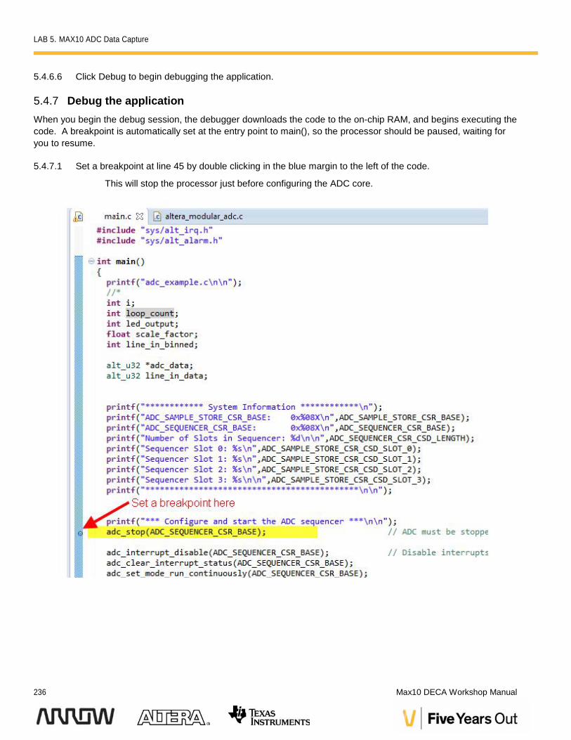
5.4.7.1 Set a breakpoint at line 45 by double clicking in the blue margin to the left of the code.
This will stop the processor just before configuring the ADC core.
LAB 5. MAX10 ADC Data Capture
Version 15.0 237
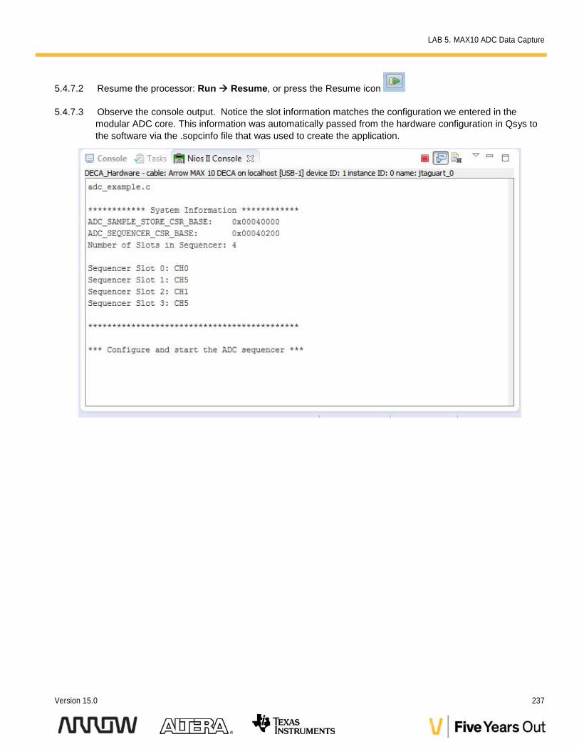
5.4.7.2 Resume the processor: Run Resume, or press the Resume icon
5.4.7.3 Observe the console output. Notice the slot information matches the configuration we entered in themodular ADC core. This information was automatically passed from the hardware configuration in Qsys tothe software via the .sopcinfo file that was used to create the application.
LAB 5. MAX10 ADC Data Capture
238 Max10 DECA Workshop Manual
5.4.7.4 Open SignalTap Analyzer: From Quartus, Tools SignalTap II Logic Analyzer.
The Deca_tap_nios.stp system should open.
5.4.7.5 Start the Analyzer in repetitive trigger mode: Processing Autorun Analysis, or press the autorun icon
. The trigger condition has been configured to trigger on reads OR writes to the ADC (see this on theSetup tab), so every time Nios accesses the ADC, the Logic Analyzer should trigger, making it easy tounderstand how the system functions.
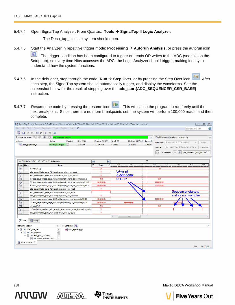
5.4.7.6 In the debugger, step through the code: Run Step Over, or by pressing the Step Over icon . Aftereach step, the SignalTap system should automatically trigger, and display the waveforms. See thescreenshot below for the result of stepping over the adc_start(ADC_SEQUENCER_CSR_BASE)instruction.
5.4.7.7 Resume the code by pressing the resume icon . This will cause the program to run freely until thenext breakpoint. Since there are no more breakpoints set, the system will perform 100,000 reads, and thencomplete.
LAB 5. MAX10 ADC Data Capture
Version 15.0 239
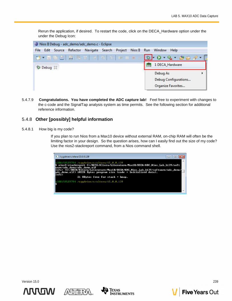
Rerun the application, if desired. To restart the code, click on the DECA_Hardware option under theunder the Debug Icon:
5.4.7.9 Congratulations. You have completed the ADC capture lab! Feel free to experiment with changes tothe c-code and the SignalTap analysis system as time permits. See the following section for additionalreference information.
5.4.8 Other [possibly] helpful information
5.4.8.1 How big is my code?
If you plan to run Nios from a Max10 device without external RAM, on-chip RAM will often be thelimiting factor in your design. So the question arises, how can I easily find out the size of my code?Use the nios2-stackreport command, from a Nios command shell.
LAB 5. MAX10 ADC Data Capture
240 Max10 DECA Workshop Manual
5.4.8.2 What other signals are connected to the ADC on the DECA board?
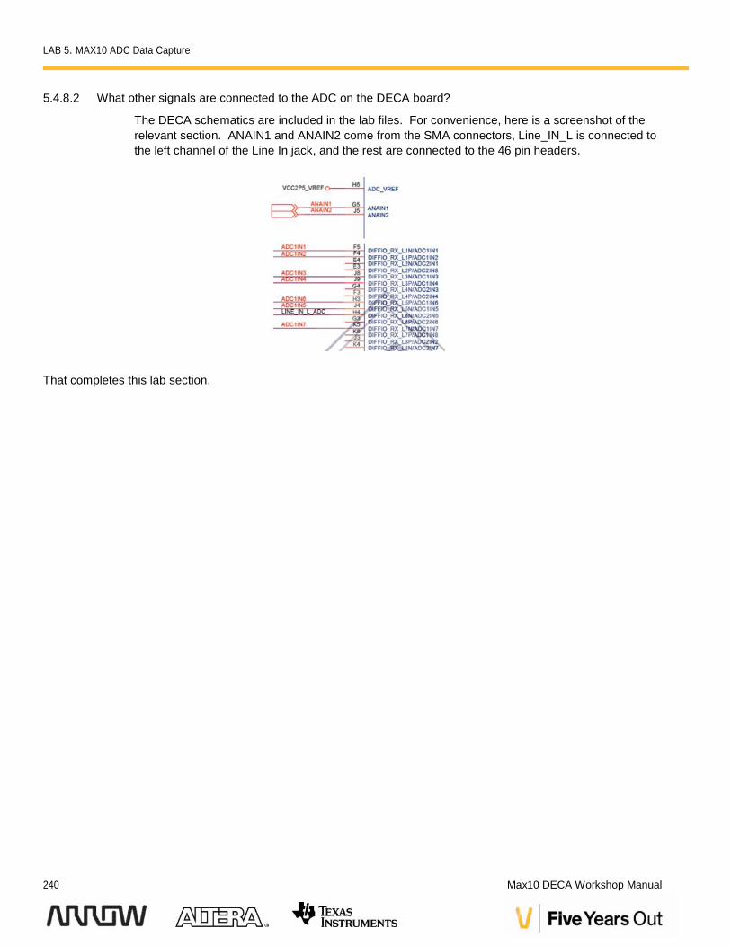
The DECA schematics are included in the lab files. For convenience, here is a screenshot of therelevant section. ANAIN1 and ANAIN2 come from the SMA connectors, Line_IN_L is connected tothe left channel of the Line In jack, and the rest are connected to the 46 pin headers.
That completes this lab section.