max14502 hi-spee usb-to-sd ar reaers it bypass · mp3 players digital still cameras ... ordering...
TRANSCRIPT

General DescriptionThe MAX14502 USB-to-SD™ card reader provides a means for portable devices that support full-speed USB communication (12Mbps) with one or two SD card slots, upgrading the USB SD card reader function to USB high-speed (480Mbps) operation. The MAX14502 has two modes of operation: Pass Thru and Card Reader. In pass thru, the SD and USB signals pass through the MAX14502 without modification, appearing like the device is not present. The host microprocessor firmware does not need modification, as there is no change from the host microprocessor’s perspective. In Card Reader mode, the MAX14502 implements a high-speed USB card reader that operates independently of the host microprocessor. All the capabilities of the full-speed USB port and SD card slot are preserved with the additional feature that allows a faster way for a PC to read or write to the SD card. The MAX14502 supports high-capacity SDHC cards. The 40-pin TQFN version supports one SD card, while the 56-bump wafer-level package (WLP) version supports two SD cards.The MAX14502 features advanced power-saving modes to reduce power consumption in portable applications. The low-power sleep modes allow the ability to disable internal circuit blocks, providing power-saving operating modes. The default clock input for is specified in the ordering information. The MAX14502 features the option to change the default values using the I2C interface.The MAX14502 is available in a 5mm x 5mm, 40-pin TQFN package. This device operates over a wide supply voltage range and is specified over the -40°C to +85°C extended temperature range.
Applications Cell Phones PDAs MP3 Players Digital Still Cameras GPS
Benefits and Features USB 2.0 High-Speed and Full-Speed Compliant SDHC Card Support Internal High-Speed USB SD Card Reader Eases
Host μP Overhead On-Chip Termination and Pullup Resistors Accommodates Clock Input Frequencies:
26MHz, 19.2MHz, 13MHz, and 12MHz Internal Clock Squarer for Low-Amplitude TCXO
Signals No Power-Supply Sequencing Required Compatible with +1.8V to +3.3V I/O Host
Microprocessor Simple Control Mode Requires Only a Single GPIO I2C Control Provides Multiple Configuration Options On-Chip Power-On Reset/Brown-Out Reset
19-4117; Rev 3; 6/16
SD is a trademark of the SD Card Association.
Note: All devices are specified over the -40°C to +85°C operating temperature range.+Denotes a lead(Pb)-free/RoHS-compliant package.**EP = Exposed pad.
PARTINPUT
FREQUENCY(MHz)
SD CARDS
PIN-PACKAGE
MAX14502AETL+ 19.2 1 40 TQFN-EP**
Ordering Information/Selector Guide
MAX14502 Hi-Speed USB-to-SD Card Readers with Bypass
EVALUATION KIT AVAILABLE

(All voltages referenced to GND.)VCC ..........................................................................-0.3V to +4VVSD ..........................................................................-0.3V to +4VVIO ...........................................................................-0.3V to +4VVTM ..........................................................................-0.3V to +4VKVBUS ....................................................................-0.3V to +4VCLDO.......................................................................-0.3V to +2VCDAT1_[3:0], HDAT1_[3:0], CCMD1, HCMD1, CCLK1, HCLK1,
CCRD_PRST, HCRD_PRST ................ -0.3V to (VSD + 0.3V)BUSY, BERR/INT, MODE, SCL, SDA, I2C_SEL,
ADD, RST .............................................. -0.3V to (VIO + 0.3V)CD+, CD-, HD+, HD-, RREF, FREF ......... -0.3V to (VTM + 0.3V)
Continuous Power Dissipation (TA = +70°C) 40-Pin TQFN (derate 35.7mW/°C above +70°C) ......2857mW
Junction-to-Case Thermal Resistance (θJC) (Note 1) 40-Pin TQFN ..............................................................1.7°C/W
Junction-to-Ambient Thermal Resistance (θJA) (Note 1) 40-Pin TQFN ...............................................................28°C/W
Operating Temperature Range ........................... -40°C to +85°CJunction Temperature ......................................................+150°CStorage Temperature Range ............................ -65°C to +160°CLead Temperature (soldering, 10s) .................................+300°C
(VCC = +2.4V to +3.6V, VSD = +2.4V to +3.6V, VIO = +1.5V to +3.6V, VTM = +2.91V to +3.4V, TA = -40°C to +85°C, unless otherwise noted. Typical values are at VCC = +3.3V, VIO = +2.5V, VSD = +2.5V, VTM = +3.3V, TA = +25°C.) (Note 2)
Note 1: Package thermal resistances were obtained using the method described in JEDEC specification JESD51-7, using a four-layer board. For detailed information on package thermal considerations, refer to www.maximintegrated.com/thermal-tutorial.
Absolute Maximum Ratings
Stresses beyond those listed under “Absolute Maximum Ratings” may cause permanent damage to the device. These are stress ratings only, and functional operation of the device at these or any other conditions beyond those indicated in the operational sections of the specifications is not implied. Exposure to absolute maximum rating conditions for extended periods may affect device reliability.
Electrical Characteristics
PARAMETER SYMBOL CONDITIONS MIN TYP MAX UNITSDC CHARACTERISTICS
VCC Supply Voltage VCC
Pass thru 2.1 3.6VCard reader active, fCCLK_ ≤ 26MHz 2.1 3.6
Card reader active, fCCLK_ > 26MHz 2.4 3.6
VSD Supply Voltage VSD
Pass thru 2.0 3.6VCard reader active, fCCLK_ ≤ 26MHz 2.0 3.6
Card reader active, fCCLK_ > 26MHz 2.4 3.6Logic Interface Supply Voltage VIO 1.5 3.6 VUSB Supply Voltage VTM 2.91 3.4 V
Digital Core LDO Regulator Output Voltage VCLDO CCLDO = 1.0µF 1.8 V
VCC Supply Current ICCPass thru 5 15 µACard reader active 35 50 mA
VSD Supply Current ISDPass thru 17 40 µACard reader active 3 mA
VIO Supply Current IIOPass thru 2 10 µACard reader active 0.2 mA
VTM Supply Current ITMPass thru 13 50 µACard reader active 25 mA
VSD Comparator Threshold VSDCT 1.0 1.5 1.9 VVTM Comparator Threshold VTMCT 2.0 2.5 2.9 VMODE, I2C_SEL, ADD, RST Input-Voltage Low VIL 0.4 V
MAX14502 Hi-Speed USB-to-SD CardReaders with Bypass
www.maximintegrated.com Maxim Integrated 2

(VCC = +2.4V to +3.6V, VSD = +2.4V to +3.6V, VIO = +1.5V to +3.6V, VTM = +2.91V to +3.4V, TA = -40°C to +85°C, unless otherwise noted. Typical values are at VCC = +3.3V, VIO = +2.5V, VSD = +2.5V, VTM = +3.3V, TA = +25°C.) (Note 2)
Electrical Characteristics (continued)
PARAMETER SYMBOL CONDITIONS MIN TYP MAX UNITSMODE, I2C_SEL, ADD, RST Input-Voltage High VIH
2/3 x VIO
V
BUSY, BERR/INT Output-Voltage Low VOL ILOAD = 1mA 0.4 V
BUSY, BERR/INT Output-Voltage High VOH ILOAD = -1mA VIO -
0.4 V
I2C_SEL, ADD, RST Input Leakage Current IIL -1 +1 µA
MODE Input Resistance to GND RMODE 150 300 500 kΩFREF Full-Swing Input-Voltage High VIH 1.3 V
FREF Full-Swing Input-Voltage Low VIL 0.4 V
FREF Low-Amplitude Input- Voltage Low VIL 200 mV
FREF Input Leakage Current IILF Full-Swing mode -10 +10 µAFREF Input Resistance Low-Amplitude input mode 1 MΩKVBUS Comparator Threshold VTH 1.0 1.25 1.5 VKVBUS Comparator Hysteresis VHYS 20 mVKVBUS Comparator Input Impedance RIN 10 MΩ
SDA/SCL Input Low Voltage VIL_I2C0.3 x VIO
V
SDA/SCL Input High Voltage VIH_I2C0.7 x VIO
V
SDA Output Logic-Low VOL_I2C
VIO > +2V, 3mA sink current 0 0.4V
VIO ≤ +2V, 3mA sink current 0 0.2 x VIO
SDA/SCL Input Leakage Current IIN_I2C -10 +10 µASD CARD INTERFACEOn-Resistance RON VTEST = 0 or VSD, ITEST = 10mA (Note 3) 10 ΩOff-Leakage Current IILSD VTEST = 0 or VSD (Note 3) -1 +1 µAOff-Capacitance CSD_OFF (Note 4) 5 pFOn-Capacitance CSD_ON (Note 5) 10 pFPullup Resistance RPU CCMD1, CDAT1_[3:0] 50 75 100 kΩ
Output High Voltage VOH IOH = -100μA 0.75 x VSD
V
Output Low Voltage VOL IOL = 100µA 0.125 x VSD
V
MAX14502 Hi-Speed USB-to-SD CardReaders with Bypass
www.maximintegrated.com Maxim Integrated 3

(VCC = +2.4V to +3.6V, VSD = +2.4V to +3.6V, VIO = +1.5V to +3.6V, VTM = +2.91V to +3.4V, TA = -40°C to +85°C, unless otherwise noted. Typical values are at VCC = +3.3V, VIO = +2.5V, VSD = +2.5V, VTM = +3.3V, TA = +25°C.) (Note 2)
PARAMETER SYMBOL CONDITIONS MIN TYP MAX UNITS
Input High Voltage VIH
VSD < 2.4V 0.8 x VSD
V
VSD ≥ 2.4V 0.625 x VSD
Input Low Voltage VIL
VSD < 2.4V 0.2 x VSD
V
VSD ≥ 2.4V 0.25 x VSD
USB INTERFACEOn-Resistance RON VCD_ = 0 or VTM, switch closed 5 Ω
On-Resistance Flatness RONFLAT VCD_ = 0 to 3.3V, VTM = +3.3V 2 Ω
On-Capacitance CON_USBSwitch closed, measured from CD+ and CD- 12 pF
Off-Capacitance COFF_USBSwitch open, measured from CD+, CD-, HD+, HD- 6 pF
AC CHARACTERISTICS (Note 6)SD CARD CLOCK TIMING (CCLK1), DEFAULT SPEED (Figure 5a)Clock Low Time tWL CL = 10pF 19 ns
Clock High Time tWH CL = 10pF 19 ns
Clock Rise Time tTLH CL = 10pF 10 ns
Clock Fall Time tTHL CL = 10pF 10 ns
SD CARD CLOCK TIMING (CCLK1), HI-SPEED (Figure 5b)Clock Low Time tWL CL = 40pF 7 ns
Clock High Time tWH CL = 40pF 7 ns
Clock Rise Time tTLH CL = 40pF 3 ns
Clock Fall Time tTHL CL = 40pF 3 ns
SD CARD COMMAND TIMING (CCMD1, CCMD2) (Figure 5b)Input Setup Time tISU 5 ns
Input Hold Time tIH 2 ns
Output Delay Time During Data Transfer Mode tODLY 14 ns
Output Hold Time tOH 2.5 nsI2C CHARACTERISTICSSCL Clock Frequency fSCL 400 kHzSDA, SCL Capacitance CIO_I2C 5 pFSDA Output Fall Time tOF_I2C 250 nsHold Time After Repeated START tHD,STA 0.6 µs
Electrical Characteristics (continued)
MAX14502 Hi-Speed USB-to-SD CardReaders with Bypass
www.maximintegrated.com Maxim Integrated 4

(VCC = +2.4V to +3.6V, VSD = +2.4V to +3.6V, VIO = +1.5V to +3.6V, VTM = +2.91V to +3.4V, TA = -40°C to +85°C, unless otherwise noted. Typical values are at VCC = +3.3V, VIO = +2.5V, VSD = +2.5V, VTM = +3.3V, TA = +25°C.) (Note 2)
(VCC = +2.4V to +3.6V, VSD = +2.4V to +3.6V, VIO = +1.5V to +3.6V, VTM = +2.91V to +3.4V, TA = -40°C to +85°C, unless otherwise noted. Typical values are at VCC = +3.3V, VIO = +2.5V, VSD = +2.5V, VTM = +3.3V, TA = +25°C.) (Note 2)
PARAMETER SYMBOL CONDITIONS MIN TYP MAX UNITSClock Low Period tLOW_I2C 1.3 µsClock High Period tHIGH_I2C 0.6 µsSetup Time for Repeated START tSU,STA 0.6 µsHold Time for Data tHD,DAT 0 0.9 µsSetup Time for Data tSU,DAT 100 nsSDA/SCL Input Fall Time tF_I2C 300 nsSDA/SCL Rise Time tR_I2C 300 nsSetup Time for STOP tSU,STO 0.6 µsBus Free Time Between STOP and START tBUF 1.3 µs
PARAMETER SYMBOL CONDITIONS MIN TYP MAX UNITSDC CHARACTERISTICS
High-Speed Squelch Detection Threshold (Diff Signal Amplitude) VHSSQ (Note 6) 100 150 mV
High-Speed Differential Input Signaling Levels VIL
Specified by high-speed receive eye diagram
High-Speed Data Signaling Common-Mode Voltage Range SCM (Note 6) -50 +500 mV
High-Speed Idle Level VHSOI -10 +10 mV
High-Speed Data Signaling High VHSOH 360 440 mV
High-Speed Data Signaling Low VHSOL -10 +10 mV
Chirp J Level (Differential Voltage) VCHIRPJ 700 1100 mV
Chirp K Level (Differential Voltage) VCHIRPK -900 -500 mV
Termination Voltage (High-Speed) VHSTERM -10 +10 mV
AC CHARACTERISTICSRise Time tHSR (Note 6) 500 ps
Fall Time tHSF (Note 6) 500 ps
Driver Waveform Requirements Specified by high-speed transmit eye diagram
See the Typical Operating Characteristics section
Driver-Output Resistance ZHSDRV 40.5 49.5 Ω
Source Jitter Total (Including Frequency Tolerance) Specified by high-speed transmit eye diagram See the Typical Operating
Characteristics section
Electrical Characteristics (continued)
USB High-Speed Source Electrical Characteristics
MAX14502 Hi-Speed USB-to-SD CardReaders with Bypass
www.maximintegrated.com Maxim Integrated 5

Note 2: All parameters are tested at TA = +25°C. Specifications over temperature are guaranteed by design.Note 3: On-resistance is measured by applying voltage and current on the SD card interface (CCLK1, CCMD1, CDAT1_[3:0]).Note 4: Off-capacitance measured with SD switch open (CCLK1, HCLK1, CCMD1, HCMD1, CDAT1_[3:0], HDAT1_[3:0]).Note 5: On-capacitance measured on SD card side (CCLK1, CCMD1, CDAT1_[3:0]).Note 6: Specifications guaranteed by design.
(VCC = +2.4V to +3.6V, VSD = +2.4V to +3.6V, VIO = +1.5V to +3.6V, VTM = +2.91V to +3.4V, TA = -40°C to +85°C, unless otherwise noted. Typical values are at VCC = +3.3V, VIO = +2.5V, VSD = +2.5V, VTM = +3.3V, TA = +25°C.) (Note 2)
USB Full-Speed Source Electrical Characteristics
PARAMETER SYMBOL CONDITIONS MIN TYP MAX UNITSDC CHARACTERISTICSSE Receiver Input High VIH 2.0 VSE Receiver Input Low VIL 0.8 VDifferential Common-Mode Voltage VCM 0.8 2.0 V
Receiver Differential Input Sensitivity VDI 0.2 V
Transmitter High VOH RL = 15kΩ connected to GND 2.8 3.6 VTransmitter Low VOL RL = 1.5kΩ connected to 3.3V 0 0.3 VTransmitter Output Signal Crossover Voltage VCRS (Note 6) 1.3 2.0 V
Bus Pullup Resistor on Upstream Facing Port (Idle Bus) RPUI 0.900 1.25 1.575 kΩ
Bus Pullup Resistor on Upstream Facing Port (Upstream Port Receiving)
RPUA 1.425 2.5 3.090 kΩ
Input Impedance ZINP 300 kΩTermination Voltage for Upstream Facing Port Pullup (RPU) VTERM VTM V
AC CHARACTERISTICSRise Time tFR 4 20 nsFall Time tFF 4 20 nsDifferential Rise and Fall Time Matching tFRFM (Note 6) 90 111.11 %
Full-Speed Data Rate tFDRATHS 11.994 12.030 Mbps
MAX14502 Hi-Speed USB-to-SD CardReaders with Bypass
www.maximintegrated.com Maxim Integrated 6

(VCC = +3.3V, VIO = +2.5V, VSD = +2.5V, VTM = +3.3V, TA = +25°C, unless otherwise noted.)Typical Operating Characteristics
0
2
6
4
8
10
0.9 1.71.3 2.1 2.5 2.9 3.3
USB ON-RESISTANCEvs. USB COMMON VOLTAGE (VCD_)
MAX
1450
2 to
c02
VCD_ COMMON VOLTAGE (V)R O
N (Ω
)
VTM = 3.3V
0
10
5
20
15
30
25
35
0 1.00.5 1.5 2.0 2.5
SD CHANNEL ON-RESISTANCEvs. SD CHANNEL COMMON VOLTAGE
MAX
1450
2 to
c03
SD CHANNEL COMMON VOLTAGE (V)
SD C
HANN
EL O
N-RE
SIST
ANCE
(Ω)
VSD = +3V
0
2
1
4
3
5
6
2.0 2.82.4 3.2 3.6
PASS THRU VCC SUPPLY CURRENTvs. SUPPLY VOLTAGE
MAX
1450
2 to
c04
VCC SUPPLY VOLTAGE (V)
SUPP
LY C
URRE
NT (µ
A)
NO CLOCK
4
3
2
1
01.5 2.41.8 2.1 2.7 3.0 3.3
PASS THRU VIO SUPPLY CURRENTvs. SUPPLY VOLTAGE
MAX
1450
2 to
c05
VIO SUPPLY VOLTAGE (V)
SUPP
LY C
URRE
NT (µ
A)
NO CLOCK
HI-SPEED EYE DIAGRAMFOR CARD READER MODE
MAX14502 toc01
UNIT TIME INTERVAL
DIFF
EREN
TIAL
VOL
TAGE
0
10
5
20
15
25
30
1.8 3.3
PASS THRU VSD SUPPLY CURRENTvs. SUPPLY VOLTAGE
MAX
1450
2 to
c06
VSD SUPPLY VOLTAGE (V)
SUPP
LY C
URRE
NT (µ
A)
2.42.1 2.7 3.0
NO CLOCK
Maxim Integrated 7www.maximintegrated.com
MAX14502 Hi-Speed USB-to-SD Card Readers with Bypass

(VCC = +3.3V, VIO = +2.5V, VSD = +2.5V, VTM = +3.3V, TA = +25°C, unless otherwise noted.)Typical Operating Characteristics (continued)
0
2
6
4
8
10
-40 10-15 35 60 85
PASS THRU VCC SUPPLY CURRENTvs. TEMPERATURE
MAX
1450
2 to
c07
TEMPERATURE (°C)
SUPP
LY C
URRE
NT (µ
A)
NO CLOCK33
32
31
30
292.0 2.82.4 3.2 3.6
CARD READER VCC SUPPLY CURRENTvs. SUPPLY VOLTAGE
MAX
1450
2 to
c08
VCC SUPPLY VOLTAGE (V)
SUPP
LY C
URRE
NT (m
A)DEVICE ENUMERATEDDATA RATE = 0Mbps
17
19
18
21
20
22
23
2.9 3.4
CARD READER VTM SUPPLY CURRENTvs. SUPPLY VOLTAGE
MAX
1450
2 to
c009
VTM SUPPLY VOLTAGE (V)
SUPP
LY C
URRE
NT (m
A)
3.13.0 3.2 3.3
DEVICE ENUMERATEDDATA RATE = 0Mbps
0
-200.1 1 10 100 1000
PASS THRU USB CHANNELFREQUENCY RESPONSE
-16
MAX
1450
2 to
c10
FREQUENCY (MHz)
ON-L
OSS
(dB)
-12
-8
-4-6
-10
-14
-18
-2
0.1 1 10 100 1000
PASS THRU SD CHANNELOFF-ISOLATION
MAX
1450
2 to
c11
FREQUENCY (MHz)
OFF-
ISOL
ATIO
N (d
B)
0
-80
-60
-40
-20
Maxim Integrated 8www.maximintegrated.com
MAX14502 Hi-Speed USB-to-SD Card Readers with Bypass

Pin DescriptionPIN NAME FUNCTION
INPUTS/OUTPUTS
1 I2C_SEL I2C Select Input. I2C_SEL must be connected to VIO or GND at power-up. Drive I2C_SEL low to disable I2C control and drive I2C_SEL high to enable I2C control.
2 SCL I2C Serial-Clock Input. SCL is +3.6V tolerant and the high threshold is set by VIO. If the I2C interface is not used, connect SCL to GND.
3 SDA I2C Serial-Data I/O. SDA is +3.6V tolerant and the high threshold is set by VIO. If the I2C interface is not used, connect SDA to GND.
4 ADD I2C Address Selection Input. Connect ADD to VIO or GND to select between two I2C slave addresses: (GND = 1110 000Xb and VIO = 1110 001Xb).
6 BERR/INTCard Reader Error/Interrupt Output. BERR/INT becomes BERR for simple control and INT for I2C control. BERR/INT goes low to indicate an error in Card Reader mode during simple control and asserts for enabled interrupts during I2C control.
7 BUSY Busy Output. BUSY asserts low to indicate device is in Card Reader mode.
8 MODECard Reader/Pass Thru Mode Select Input. MODE is only active during simple control. Drive MODE low to enable Pass Thru mode and drive MODE high to enable Card Reader mode. For I2C control, MODE must be connected to GND.
9 RST Reset Input. Drive RST low to reset the internal registers to default values and put all outputs in high impedance. Connect RST to VIO for normal operation.
25 FREF
Frequency Input. FREF is the clock input (12MHz/13MHz/19.2MHz/26MHz) for the internal logic and USB PHY. FREF can accept a square-wave or sine-wave clock. An internal clock squaring circuit can be enabled or disabled through I2C. In simple control, the internal clock squarer is enabled by default.
27 RREF Reference Resistor. Connect a Bias Resistor 6.19kΩ ±1% from RREF to GND.USB INTERFACE
22 CD+ USB Analog Switch/High-Speed USB Transceiver. CD+ connects to D+ on the USB connector.
21 CD- USB Analog Switch/High-Speed USB Transceiver. CD- connects to D- on the USB connector.
20 HD+ USB Analog Switch. HD+ connects to D+ on the host side.
19 HD- USB Analog Switch. HD- connects to D- on the host side.
28 KVBUS USB Bus Power-Supply Detection Input. Connect a resistor-divider between USB VBUS, KVBUS, and GND.
SD CARD INTERFACE
13 CDAT1_0 SD Card 1 Data Bus Analog Switch/Card Reader Interface. CDAT1_0 connects to DAT0 on the SD card.
12 CDAT1_1 SD Data Card 1 Bus Analog Switch/Card Reader Interface. CDAT1_1 connects to DAT1 on the SD card.
11 CDAT1_2 SD Data Card 1 Bus Analog Switch/Card Reader Interface. CDAT1_2 connects to DAT2 on the SD card.
10 CDAT1_3 SD Card 1 Data Bus Analog Switch/Card Reader Interface. CDAT1_3 connects to DAT3 on the SD card.
34 CCMD1 SD Card 1 Command Analog Switch/Card Reader Interface. CCMD1 connects to CMD on the SD card.
32 CCLK1 SD Card 1 Clock Analog Switch/Card Reader Interface. CCLK1 connects to CLK on the SD card.
MAX14502 Hi-Speed USB-to-SD CardReaders with Bypass
www.maximintegrated.com Maxim Integrated 9

Pin Description (continued)PIN NAME FUNCTION
33 CCRD_PRST SD Card 1 Analog Switch for Card Present Detection. CCRD_PRST is the card detection line to the SD socket. When in Pass Thru mode, CCRD_PRST is connected to HCRD_PRST.
17 HDAT1_0 SD Card 1 Data Bus Analog Switch. HDAT1_0 connects to DAT0 on the SD port of the host µP.
16 HDAT1_1 SD Card 1 Data Bus Analog Switch. HDAT1_1 connects to DAT1 on the SD port of the host µP.
15 HDAT1_2 SD Card 1 Data Bus Analog Switch. HDAT1_2 connects to DAT2 on the SD port of the host µP.
14 HDAT1_3 SD Card 1 Data Bus Analog Switch. HDAT1_3 connects to DAT3 on the SD port of the host µP.
31 HCMD1 SD Card 1 Command Analog Switch. HCMD1 connects to CMD on the SD port of the host µP. 29 HCLK1 SD Card 1 Clock Analog Switch. HCLK1 connects to CLK on the SD port of the host µP.
30 HCRD_PRST SD Card 1 Analog Switch for Card Present Detection. HCRD_PRST is connected to CCRD_PRST in Pass Thru mode.
POWER SUPPLY
5 VIOI/O Logic-Level Translator Voltage. Bypass VIO to GND with a 0.1µF ceramic capacitor. VIO powers the logic inputs/outputs and I2C block.
23 VTMUSB Analog Switch and Transceiver Power Supply. Bypass VTM to GND with a 0.1µF ceramic capacitor.
38 CLDO Bypass Capacitor for Internal +1.8V LDO. Connect a 1µF ceramic capacitor (X7R, X5R, or better) from CLDO to GND. CLDO must not be used to power external circuitry.
39 VCC Digital Supply Voltage. Bypass VCC to GND with a 1µF ceramic capacitor (X7R, X5R, or better).
40 VSD SD Card Voltage. Bypass VSD to GND with a 1µF ceramic capacitor (X7R, X5R, or better).
18, 24, 26, 37 GND GroundNO CONNECTION
35, 36 N.C. No Connection. Connect N.C. to GND. EXPOSED PAD
— EP Exposed Pad. Connect EP to GND. Do not use EP as the sole GND connection.
MAX14502 Hi-Speed USB-to-SD CardReaders with Bypass
www.maximintegrated.com Maxim Integrated 10

Figure 1. Typical Application Circuit for Simple Control Mode with One SD Card
USBUSBCONNECTOR
D+
D-
SD SLOT
SIMPLE CONTROL
VIO
FREFVBUS
SD CARDINTERFACE
VSD
VCC
MODE
I2C_SEL
ADD
SDA
SCL
USB HSCARD READER
VSD
44
GND
HCRD_PRST
HCLK1HCMD1
HDAT1_[3:0]
CCRD_PRSTCCLK1CCMD1CDAT1_[3:0]
CLDO
KVBUS
CD+
CD-
HD+
HD-
USBTRANSCEIVER
VCCBERRBUSY
VTM
USB SWITCHES
VTM
SD PORT 1 SWITCHES
RREF
I/O LEVELTRANSLATORS
VIO
HOST I/O
HOSTPROCESSOR
SDPORT
MAX14502
MAX14502 Hi-Speed USB-to-SD CardReaders with Bypass
www.maximintegrated.com Maxim Integrated 11

Figure 2. Typical Application Circuit for I2C Control Mode with One SD Port and Two SD Cards
USBCONNECTOR
D+
D-
VBUS
GND
USB
HOST I/O
HOSTPROCESSOR
SDPORT
VIO
VTM
SD SLOT1
FREF
SD CARDINTERFACE
VSD
VCC MODE
INT
I2C_SEL
SDASCL
USB HSCARD READER
44
HCRD_PRST
HCLK1HCMD1
HDAT1_[3:0]
CCRD_PRST
CCLK1CCMD1CDAT1_[3:0]
CLDO
CD+
CD-
HD+
HD-
USBTRANCEIVER
SD SLOT24
HCLK2
HCMD2HDAT2_[3:0]
CCLK2CCMD2CDAT2_[3:0]
BUSY
VIOADD
VIO
OPTIONAL
RREF
KVBUS
SD PORT 2 SWITCHES
SD PORT 1 SWITCHES
VCC
VSD
I/O LEVELTRANSLATORS
VTM
USB SWITCHES
MAX14502
I2C CONTROL
MAX14502 Hi-Speed USB-to-SD CardReaders with Bypass
www.maximintegrated.com Maxim Integrated 12
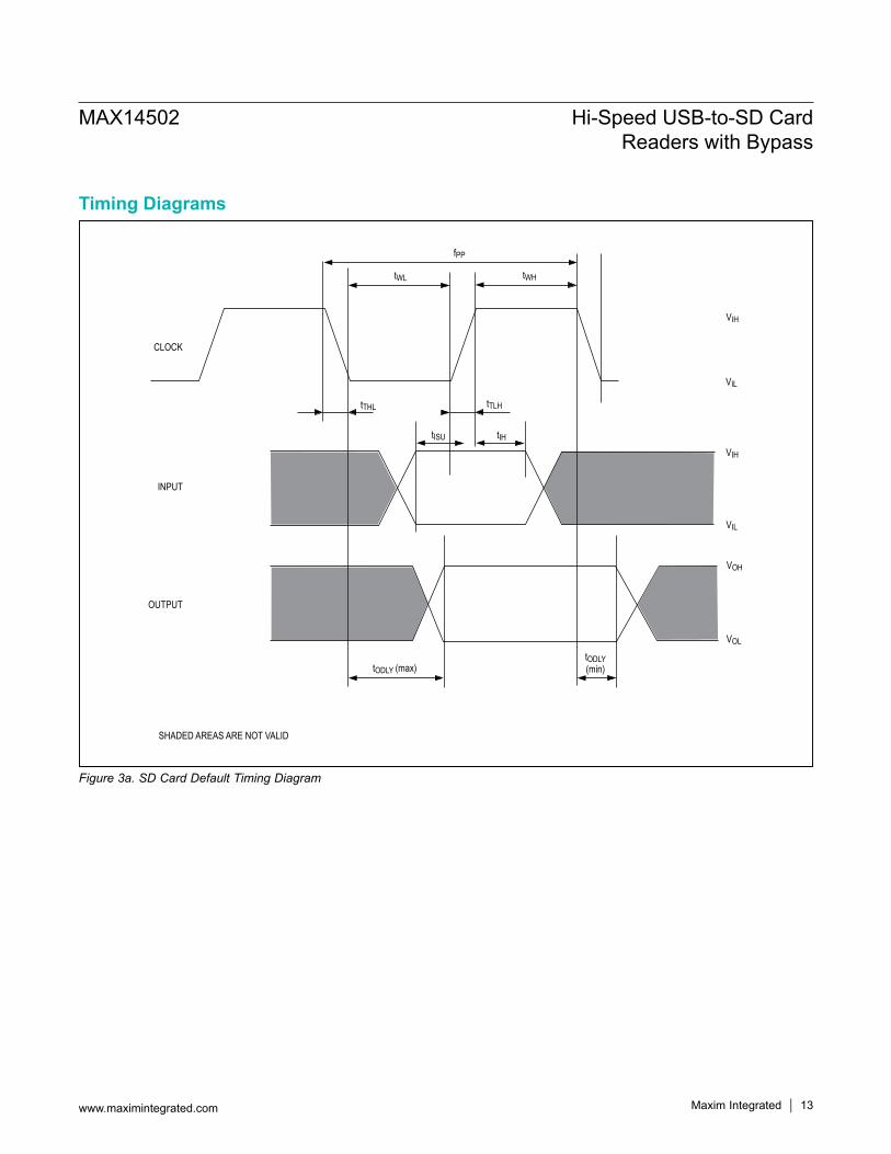
Figure 3a. SD Card Default Timing Diagram
Timing Diagrams
fPP
tWL tWH
tTLH
tIH
tODLY(min)
SHADED AREAS ARE NOT VALID
tTHL
tISU
tODLY (max)
VIH
VIL
VIH
VIL
VOH
VOL
CLOCK
INPUT
OUTPUT
MAX14502 Hi-Speed USB-to-SD CardReaders with Bypass
www.maximintegrated.com Maxim Integrated 13

Figure 3b. SD Card High-Speed Timing Diagram
Timing Diagrams (continued)
fPP
tWL tWH
tTLH
tIH
tTHL
tISU
tODLY tOH
VIH
VIL
VIH
VIL
VOH
VOL
CCLK1
CDAT1 _[3:0],CCMD1 (READ)
VOH
CDAT1 _[3:0],CCMD1 (WRITE)
VIH
VILVOL
MAX14502 Hi-Speed USB-to-SD CardReaders with Bypass
www.maximintegrated.com Maxim Integrated 14

Detailed DescriptionThe MAX14502 can be added to devices that have an SD card slot and a USB full-speed port (12Mbps) to provide a high-speed USB path to an SD card bypassing the host microprocessor (μP), allowing for faster SD card transfers (Figure 1 through Figure 4). Without the MAX14502, a host μP with a full-speed USB port moves data between an SD card and a host PC at 12Mbps when transferring data from an SD card through USB. The host μP has additional overhead because it has to accept data from the SD cards, process the data by putting it in USB format, and then transfer the data through the USB port. The MAX14502 create an alternate path from the SD card to USB, providing USB high-speed capability. By bypassing the host μP using the MAX14502, SD card read and write operations are not limited by host μP overhead and USB full-speed data rates.The MAX14502 operate in Pass Thru and Card Reader mode. In Pass Thru mode, the MAX14502 is transparent to the host μP. All read and write operations pass from the host μP SD port to the SD card without modification. All of the features of the original device are intact and there is no need to change firmware in the host μP. In Card Reader mode, the SD card is connected to the PC with the internal USB high-speed card reader, bypassing the host μP.
The MAX14502 can be controlled using a simple control method that employs a single output from a μP or ASIC to select Pass Thru or Card Reader mode. The SD card can be used as a high-speed USB card reader in simple control. I2C control allows more configuration options and provides status information along with error conditions and additional interrupts. The state of I2C_SEL must not change after VIO is applied.With I2C control, the I2C bus is used to read and write to internal registers for configuration, error checking, control, and status reporting. The control and configuration registers have various functions including wakeup, interrupt enable, and SD switch settings. The status registers give the status of errors, SD card detection, power supplies, and interrupts. Putting the MAX14502 to sleep puts the device into Pass Thru mode. Some I2C commands are executed upon waking up or entering Card Reader mode. For register settings that involve Card Reader mode, (when in Sleep mode), program-ming the I2C registers changes the values, but the actions do not execute until the internal logic wakes up or Card Reader mode is entered. The register map indicates when register bit changes take effect.
Figure 4. I2C Timing Diagram
Timing Diagrams (continued)
SDA
SCL
tHD,STA
tLOW_I2C
tHIGH_I2C
tR_I2C tF_I2C
tSU,DAT tSU,STAtSU,STO
tBUFtHD,STA
tHD,DAT
STARTCONDITION
STOPCONDITION
STARTCONDITION
REPEATEDSTART CONDITION
tF_I2C
tR_I2C
MAX14502 Hi-Speed USB-to-SD CardReaders with Bypass
www.maximintegrated.com Maxim Integrated 15
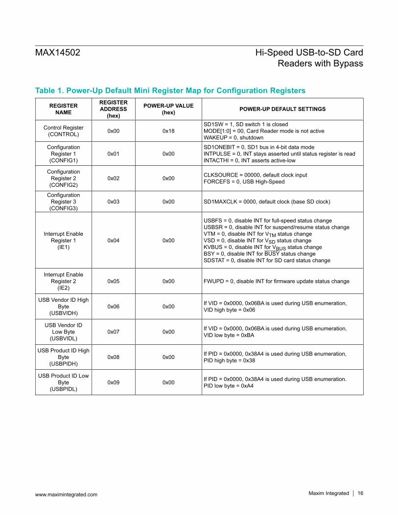
Table 1. Power-Up Default Mini Register Map for Configuration Registers
REGISTER NAME
REGISTER ADDRESS
(hex)
POWER-UP VALUE (hex) POWER-UP DEFAULT SETTINGS
Control Register (CONTROL) 0x00 0x18
SD1SW = 1, SD switch 1 is closed MODE[1:0] = 00, Card Reader mode is not active WAKEUP = 0, shutdown
Configuration Register 1 (CONFIG1)
0x01 0x00SD1ONEBIT = 0, SD1 bus in 4-bit data mode INTPULSE = 0, INT stays asserted until status register is read INTACTHI = 0, INT asserts active-low
Configuration Register 2 (CONFIG2)
0x02 0x00 CLKSOURCE = 00000, default clock input FORCEFS = 0, USB High-Speed
Configuration Register 3 (CONFIG3)
0x03 0x00 SD1MAXCLK = 0000, default clock (base SD clock)
Interrupt Enable Register 1
(IE1)0x04 0x00
USBFS = 0, disable INT for full-speed status change USBSR = 0, disable INT for suspend/resume status change VTM = 0, disable INT for VTM status change VSD = 0, disable INT for VSD status change KVBUS = 0, disable INT for VBUS status change BSY = 0, disable INT for BUSY status change SDSTAT = 0, disable INT for SD card status change
Interrupt Enable Register 2
(IE2)0x05 0x00 FWUPD = 0, disable INT for firmware update status change
USB Vendor ID High Byte
(USBVIDH)0x06 0x00 If VID = 0x0000, 0x06BA is used during USB enumeration,
VID high byte = 0x06
USB Vendor IDLow Byte
(USBVIDL)0x07 0x00 If VID = 0x0000, 0x06BA is used during USB enumeration,
VID low byte = 0xBA
USB Product ID High Byte
(USBPIDH)0x08 0x00 If PID = 0x0000, 0x38A4 is used during USB enumeration,
PID high byte = 0x38
USB Product ID Low Byte
(USBPIDL)0x09 0x00 If PID = 0x0000, 0x38A4 is used during USB enumeration.
PID low byte = 0xA4
MAX14502 Hi-Speed USB-to-SD CardReaders with Bypass
www.maximintegrated.com Maxim Integrated 16

Default Power-Up (Pass Thru Mode)In the default Pass Thru mode, the device is transparent and the existing host functions (access to SD cards and USB) are preserved (F . The host μP reads and writes data to the SD card from the SD port, and can communicate to a PC through its existing full-speed USB port. All of the features of the original chipset are intact. The MAX14502 sleeps when in Pass Thru mode (WAKEUP = 0), when the MODE input is low, or when the MODE bits [2:1] in control register (0x00) are set to Card Reader mode, not active. In Sleep mode, the inter-nal microcontroller is turned off and current consumption
is minimized. The settings for SD port switches for card 1 is controlled by SD port switch bits [4:3] in the control register.
Card Reader ModeIn Card Reader mode, the PC communicates with the SD card through USB with an internal high-speed SD card reader, bypassing the host μP. Figure 6 shows card reader mode with SD card 1 connected to the PC with the internal card reader. The 40-pin TQFN can connect to a single SD card in Card Reader mode.
Figure 5. Default Startup (Pass Thru Mode)
CD+
HOST PROCESSOR
USB SWITCHES
CD-
D+
D-
HD+
HD-USBUSB
CONNECTOR
SD CARD INTERFACE
USB HSCARD READER
CCRD_PRSTSD PORT 1 SWITCHES
CCLK1
CCMD1
HCRD_PRST
HCLK1
HCMD1
44 CDAT1_[3:0] HDAT1_[3:0]
SDPORT1
I/O LEVELTRANSLATORS
HOSTI/O
SDSLOT1
USBTRANSCEIVER
MAX14502
MAX14502 Hi-Speed USB-to-SD CardReaders with Bypass
www.maximintegrated.com Maxim Integrated 17
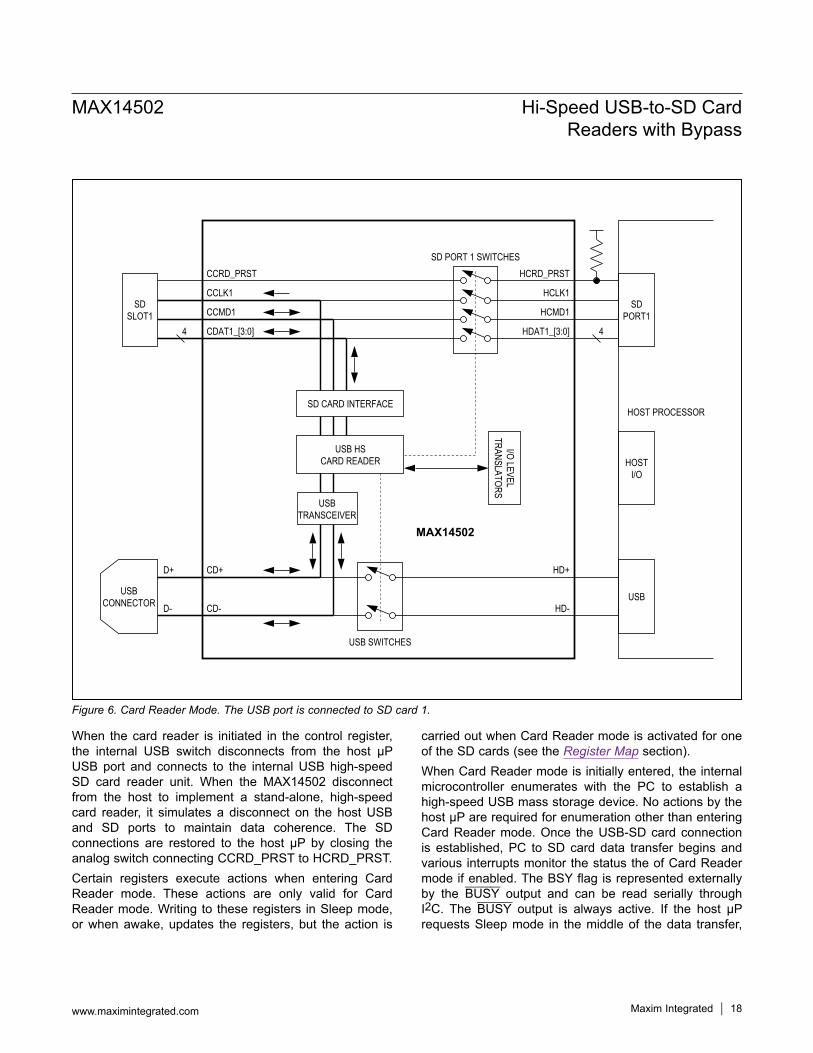
When the card reader is initiated in the control register, the internal USB switch disconnects from the host μP USB port and connects to the internal USB high-speed SD card reader unit. When the MAX14502 disconnect from the host to implement a stand-alone, high-speed card reader, it simulates a disconnect on the host USB and SD ports to maintain data coherence. The SD connections are restored to the host μP by closing the analog switch connecting CCRD_PRST to HCRD_PRST. Certain registers execute actions when entering Card Reader mode. These actions are only valid for Card Reader mode. Writing to these registers in Sleep mode, or when awake, updates the registers, but the action is
carried out when Card Reader mode is activated for one of the SD cards (see the Register Map section). When Card Reader mode is initially entered, the internal microcontroller enumerates with the PC to establish a high-speed USB mass storage device. No actions by the host μP are required for enumeration other than entering Card Reader mode. Once the USB-SD card connection is established, PC to SD card data transfer begins and various interrupts monitor the status the of Card Reader mode if enabled. The BSY flag is represented externally by the BUSY output and can be read serially through I2C. The BUSY output is always active. If the host μP requests Sleep mode in the middle of the data transfer,
Figure 6. Card Reader Mode. The USB port is connected to SD card 1.
CD+
HOST PROCESSOR
USB SWITCHES
CD-
D+
D-
HD+
HD-USBUSB
CONNECTOR
SD CARD INTERFACE
USB HSCARD READER
CCRD_PRSTSD PORT 1 SWITCHES
CCLK1
CCMD1
HCRD_PRST
HCLK1
HCMD1
44 CDAT1_[3:0] HDAT1_[3:0]
SDPORT1
I/O LEVELTRANSLATORS
HOSTI/O
SDSLOT1
USBTRANSCEIVER
MAX14502
MAX14502 Hi-Speed USB-to-SD CardReaders with Bypass
www.maximintegrated.com Maxim Integrated 18

the MAX14502 do not complete the transfer, exit Card Reader mode, reconnect USB switches, and go to sleep. Because the BUSY output (BSY bit in I2C) indicates Card Reader mode, the host μP may monitor this output after commanding a mode change to determine when the change takes place (Figure 7). If the host requests the other SD card to enter Card Reader mode, the busy flag deasserts and reasserts to let the host know that the change took place.
Simple Control (I2C_SEL = Low)The MAX14502 features a very simple control scheme for entering Card Reader mode that requires a single logic (GPIO) from the host μP. The simple control may only be used with the single SD port versions. When I2C_SEL is connected low at startup, the MODE input controls whether the device is in Pass Thru or Card Reader mode. Driving MODE low enables Pass Thru mode (Figure 8), and the host μP has a direct connection to the SD card and USB connector through internal analog switches. Driving MODE high enables Card Reader mode between SD card 1 and the PC through the USB connector (Figure 9). BERR/INT functions as the bridge error output BERR that
asserts for card reader errors. Interrupts are not enabled, the clock source is set to the default as defined by the part number, and the BERR and BUSY outputs are active. Upon MODE transitioning high, SD card 1 connects to the USB connector in Card Reader mode and BUSY asserts low. The BUSY output indicates that the device is in Card Reader mode. BUSY may be important to the host μP, as the time to complete enumeration/de-enumeration may take a long time (> 100ms).
I2C Control (I2C_SEL = High)The MAX14502 feature I2C control that allows access to internal registers for complete control over configuration, SD port analog switches, interrupts, clock configuration, advanced power-on states, and error status. I2C control uses I2C to serially program the MAX14502 to be in Card Reader or Pass Thru mode, and allows either SD card to be connected in Card Reader mode. While a SD card is connected in Card Reader mode, the other SD port analog switches can be independently controlled serially through I2C. Using the I2C bus to put the device to sleep minimizes the supply current while maintaining control over the SD port switches.
Figure 7. Card Reader Flow Chart
PASS THRU
REQUESTTO ENTER CARD
READERREQUEST
TO SLEEP ORPASS THRU
IF AWAKE
IF ASLEEP
NO SD COMMAND IN PROGRESS
SD COMMANDIN PROGRESS
• DISCONNECT SD SWITCHES FOR CARD READER• ENUMERATE SD CARD• OPEN USB SWITCHES
CARD READER(TRANSFER DATA)
• DEENUMERATE PC• CLOSE USB SWITCHES
• DEENUMERATE SD CARD• RESTORE SD SWITCHES TO I2C SETTINGS
• DEASSERT BUSY• CLEAR BUSY FLAG
• ASSERT BUSY• SET BUSY FLAG
• ENUMERATE PC
MAX14502 Hi-Speed USB-to-SD CardReaders with Bypass
www.maximintegrated.com Maxim Integrated 19

Control Register (0x00)The control register controls the settings of SD port analog switches, Card Reader mode, and sleep (Table 2.) The state of the SD port analog switches can be changed when the device is in Sleep mode or in Card Reader mode, and actions are executed immediately. Changing the card reader bits in Sleep mode does not cause the device to enter Card Reader mode. Under this condition, the MAX14502 enters Card Reader mode upon waking up.
Configuration RegistersThe MAX14502 have three configuration registers (CONFIG1 = 0x01, CONFIG2 = 0x02, CONFIG3 = 0x03). The configuration registers control the SD bus bit data mode, interrupt polarity, interrupt clearance, clock configuration, SD clock, and USB speed for Card Reader mode. The default settings are shown in the Register Map section.
Interrupts (INT)All interrupts are masked in the default reset state. There are two interrupt enable registers (IE1 = 0x04, IE2 = 0x05) and two interrupt request registers (IRQ1 = 0x10, IRQ2 = 0x11). The BERR/INT output functions as the bridge error output BERR in simple control and functions as an interrupt INT in I2C control. The polarity of INT and how INT is asserted can be programmed in CONFIG1. The INT output asserts for enabled interrupts and errors in Card Reader mode. The
Figure 8. I2C_SEL Connected Low to Enable Simple Control and MODE = 0 to Enable Pass Thru
HCRD_PRST
HCLK1
HCMD1
HDAT1_[3:0]
CD+
HOST PROCESSOR
USB SWITCHES
CD-
D+
D-
HD+
HD-USBUSB
CONNECTOR
SD CARD INTERFACE
USB HSCARD READER
CCRD_PRSTSD PORT 1 SWITCHES
CCLK1
CCMD1
BUSY
BERR
MODE = LOW
44 CDAT1_[3:0]
I2C_SEL = LOW
SDPORT1
I/O LEVELTRANSLATORS
HOSTI/O
SDSLOT 1
USBTRANSCEIVER
MAX14502
MAX14502 Hi-Speed USB-to-SD CardReaders with Bypass
www.maximintegrated.com Maxim Integrated 20

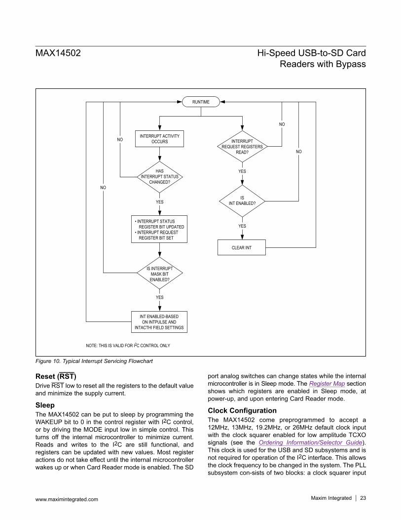
polarity of INT can be active-high or active-low, and INT can be programmed to stay asserted until the status register is read, or stay asserted for 10ms. If INT is programmed to stay asserted, a read to the status register is required to clear INT. INT can be programmed to be active-high or active-low when I2C_SEL is high (I2C control). INT is high impedance in Sleep mode (WAKEUP = 0), regardless of the INT polarity programmed in the I2C registers. Use a pullup or pulldown resistor for the desired inactive INT polarity state during Sleep mode.
Interrupt MaskingAll interrupts are masked at power-up. While masked interrupts do not assert the INT output, they do register as changes in the interrupt request registers (IRQ1 and IRQ2). The status register (STATUS1 = 0x12) indicates the current state of the interrupt bits. If interrupts are masked, polling IRQ1 and IRQ2 indicate the fields with changes, and STATUS1 gives the current state. Reading the IRQ registers resets the interrupt request bits. If polling is used to read the device status, it is required to read both the status register and the interrupt request registers to check for state changes.
USB InterruptsWhen enabled, the INT output asserts an interrupt for changes in the USB connection and if the operating system suspends the USB connection. VBUS is detected at the KVBUS input and changes in VBUS voltage can assert an interrupt when enabled.
Power-Supply InterruptsThe MAX14502 feature many advanced power-saving modes. VCC, VSD, and VTM do not need to be applied for I2C communication. Changes in VSD and VTM can assert an interrupt when enabled to indicate different power-saving modes (see the Power-Supply Modes section).
Busy InterruptWhen enabled, changes in the BSY bit can assert an interrupt (see the Busy Indication (BSY) section).
SD Status InterruptWhen enabled, the SDSTAT bit asserts an interrupt for card detection and removal upon entering Card Reader mode for the SD card socket configured as the card reader. The SDSTAT bit is not active during Pass Thru mode and does not change states in the IRQ registers upon card insertion and removal during Pass Thru mode.
Table 2. Control Register (0x00)BIT DESCRIPTION VALUE FUNCTION DEFAULT
[7:4] RESERVED 0001 Set these bits to 0001. 0001
3
SD PORT 1 ANALOG SWITCHES SD Port 1 is a set of seven analog switches connecting the SD port to the SD card. This set contains: card-present (CCRD_PRST), clock (CCLK1), command (CCMD1), and four data lines (CDAT1_[3:0]). This setting is ignored when Card Reader mode is enabled for this port.
0Analog switches are open, disconnecting the SD port from the SD card.
1
1Analog switches are closed, connecting the SD port to the SD card.
[2:1]CARD READER MODE Changing these bits in Sleep mode does not execute the action until the host µP wakes up the MAX14502.
00, 11 Card Reader mode not active.
0001 Card Reader mode active: Connects to SD card 1.
10 RFU
0
WAKEUP In Sleep mode, the MAX14502 are in Pass Thru mode. SD port switches are controlled by their respective bits. Entering Sleep mode reduces the supply current by turning off the internal logic. Request to shut down may be delayed due to USB and de-enumeration.
0 Request internal logic to shut down. 0
1 Wake up internal logic.
MAX14502 Hi-Speed USB-to-SD CardReaders with Bypass
www.maximintegrated.com Maxim Integrated 21

Error CheckingIn simple control, the BERR/INT output functions as BERR and indicates if an error occurs during Card Reader mode. If BERR asserts low to indicate an error, the MAX14502 stay in Card Reader mode. If the error clears, data transfer begins. BERR asserts if KVBUS, VTM, or VSD are not present. It is recommended that MODE be pulled low when BERR indicates an error to return the MAX14502 to Pass Thru mode for the host μP to clear the error.In I2C control, BERR/INT functions as an interrupt output (INT) and asserts for errors encountered in Card Reader mode when interrupts are not masked. To find the source of the interrupt, read the interrupt request registers and status register.
Busy Indication (BSY)The BUSY output is used in simple control and I2C control to indicate when Card Reader mode is active. In simple control, transitioning MODE high to low requests the internal microcontroller to enable Pass Thru mode. BUSY asserts low while in Card Reader mode and deasserts high in Pass Thru mode.The BSY bit in STATUS1 (0x12) behaves similarly with I2C control. The BUSY output is represented by the BSY bit. Requests to put the device to sleep or bypass (Pass Thru mode) while in Card Reader mode can be verified by checking the state of the BUSY signal or BSY bit. The BUSY output indicates the status of the BUSY flag in STATUS1. The BSY bit is 1 when the BUSY output asserts low. When enabled, changes in the busy flag cause an interrupt. In I2C control, either the BSY bit or the BUSY output give the status of the busy state.
Figure 9. I2C_SEL is connected low to enable simple control and MODE = 1 to enable Card Reader mode for SD card 1.
HCRD_PRST
HCLK1
HCMD1
HDAT1_[3:0]
CD+
HOST PROCESSOR
USB SWITCHES
CD-
D+
D-
HD+
HD-USBUSB
CONNECTOR
SD CARD INTERFACE
USB HSCARD READER
CCRD_PRSTSD PORT 1 SWITCHES
CCLK1
CCMD1
BUSY
BERR
MODE = HIGH
44 CDAT1_[3:0]
I2C_SEL = LOW
SDPORT1
I/O LEVELTRANSLATORS
HOSTI/O
SDSLOT 1
USBTRANSCEIVER
MAX14502
MAX14502 Hi-Speed USB-to-SD CardReaders with Bypass
www.maximintegrated.com Maxim Integrated 22
Reset (RST)Drive RST low to reset all the registers to the default value and minimize the supply current.
SleepThe MAX14502 can be put to sleep by programming the WAKEUP bit to 0 in the control register with I2C control, or by driving the MODE input low in simple control. This turns off the internal microcontroller to minimize current. Reads and writes to the I2C are still functional, and registers can be updated with new values. Most register actions do not take effect until the internal microcontroller wakes up or when Card Reader mode is enabled. The SD
port analog switches can change states while the internal microcontroller is in Sleep mode. The Register Map section shows which registers are enabled in Sleep mode, at power-up, and upon entering Card Reader mode.
Clock ConfigurationThe MAX14502 come preprogrammed to accept a 12MHz, 13MHz, 19.2MHz, or 26MHz default clock input with the clock squarer enabled for low amplitude TCXO signals (see the Ordering Information/Selector Guide). This clock is used for the USB and SD subsystems and is not required for operation of the I2C interface. This allows the clock frequency to be changed in the system. The PLL subsystem con-sists of two blocks: a clock squarer input
Figure 10. Typical Interrupt Servicing Flowchart
RUNTIME
NOTE: THIS IS VALID FOR I2C CONTROL ONLY
INTERRUPTREQUEST REGISTERS
READ?
ISINT ENABLED?
HASINTERRUPT STATUS
CHANGED?
IS INTERRUPTMASK BITENABLED?
YES
YES
YES
YES
• INTERRUPT STATUS REGISTER BIT UPDATED• INTERRUPT REQUEST REGISTER BIT SET
CLEAR INT
INT ENABLED-BASEDON INTPULSE AND
INTACTHI FIELD SETTINGS
INTERRUPT ACTIVITYOCCURSNO
NO
NO
NO
MAX14502 Hi-Speed USB-to-SD CardReaders with Bypass
www.maximintegrated.com Maxim Integrated 23

(enabled by default), which accepts low-signal amplitude TCXO signals (down to 200mV), and a PLL with fixed dividers. The PLL sub system can be configured using the I2C interface. The complete list of PLL subsystem combinations are listed in Table 3.
I2C Serial InterfaceSerial AddressingThe device operate as I2C slave devices that send and receive data through an I2C-compatible 2-wire interface. The interface uses a serial-data line (SDA) and a serial-clock line (SCL) to achieve bidirectional communication between master(s) and slave(s). A master initiates all data transfers to and from the MAX14502, and generates the SCL clock that synchronizes the data transfer. The SDA line operates as both an input and an open-drain output requiring a pullup resistor on SDA. The SCL line operates only as an input. A pullup resistor is required on SCL if there are multiple masters on the 2-wire interface, or if the master in a single-master system has an open-drain SCL output. Each transmission consists of a START (S) condition by a master, followed by the MAX14502’s 7-bit slave address, plus a R/W bit, a register address byte, one or more data bytes, and finally a STOP (P) condition.
START and STOP ConditionsBoth SCL and SDA remain high when the interface is idle. A master signals the beginning of a transmission with a START condition by transitioning SDA from high to low while SCL is high (Figure 11). When the master has finished communicating with the slave, it issues a STOP condition by transitioning SDA from low to high while SCL is high. The bus is then free for another transmission.
Figure 11. START and STOP Conditions
Table 3. Clock Source Bit ValuesCLKSOURCE SOURCE (MHz) NOTES
00000bSee Ordering Information/
Selector Guide
Default low-amplitude clock
00001b 19.2 Rail-to-rail square wave
00010b 19.2 Low-amplitude sine wave
00101b 13.0 Rail-to-rail square wave
00110b 13.0 Low-amplitude sine wave
01001b 12.0 Rail-to-rail square wave
01010b 12.0 Low-amplitude sine wave
01101b 26.0 Rail-to-rail square wave
01110b 26.0 Low-amplitude sine wave
All other values Same as 00000b Default clock source
SDA
SCL
START CONDITION
STOPCONDITION
S P
MAX14502 Hi-Speed USB-to-SD CardReaders with Bypass
www.maximintegrated.com Maxim Integrated 24

Bit TransferOne data bit is transferred during each clock pulse (Figure 12). The data on SDA must remain stable while SCL is high.
AcknowledgeThe acknowledge bit is a clocked 9th bit (Figure 13), which the recipient uses to handshake receipt of each byte of data. Each byte transferred effectively requires nine bits. The master generates the 9th clock pulse, and the recipient pulls down SDA during the acknowledge clock pulse. The SDA line is stable low during the high period of the clock pulse. When the master is transmitting to the MAX14502, the MAX14502 generates the acknowledge bit because the MAX14502 is the recipient. When the MAX14502 is transmitting to the master, the master generates the acknowledge bit because the master is the recipient.
Slave AddressesThe MAX14502 have a 7-bit long slave address. The bit following the 7-bit slave address is the R/W bit, which is low for a write command and high for a read command. The address bit ADD is externally driven high or low by the ADD input to select between two slave addresses to avoid conflict with other I2C addresses (Figure 14). Table 4 shows the binary values for reads and writes.
Figure 12. Bit Transfer
Figure 13. Acknowledge
Figure 14. Slave Address
Table 4. Slave AddressesADD FUNCTION DEVICE ADDRESSHigh Read 1 1 1 0 0 0 1 1
High Write 1 1 1 0 0 0 1 0
GND Read 1 1 1 0 0 0 0 1
GND Write 1 1 1 0 0 0 0 0
SDA
SCL
DATA LINE STABLE;DATA VALID
CHANGE OF DATAALLOWED
SCL
SDABY
TRANSMITTER
CLOCK PULSE FORACKNOWLEDGE
START CONDITION
SDABY
RECEIVER
1 2 8 9
S
SDA 1 ACK
SCLMSB LSB
1 0 R/W1 0 0 ADD
MAX14502 Hi-Speed USB-to-SD CardReaders with Bypass
www.maximintegrated.com Maxim Integrated 25
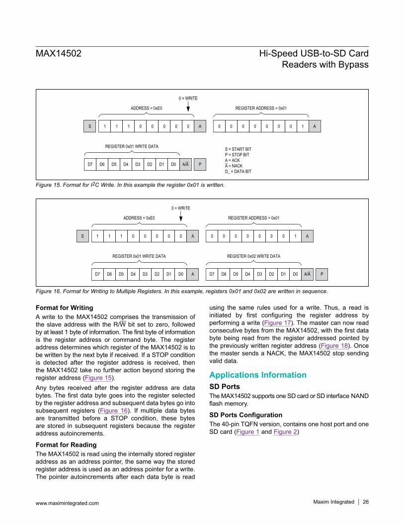
Format for WritingA write to the MAX14502 comprises the transmission of the slave address with the R/W bit set to zero, followed by at least 1 byte of information. The first byte of information is the register address or command byte. The register address determines which register of the MAX14502 is to be written by the next byte if received. If a STOP condition is detected after the register address is received, then the MAX14502 take no further action beyond storing the register address (Figure 15).Any bytes received after the register address are data bytes. The first data byte goes into the register selected by the register address and subsequent data bytes go into subsequent registers (Figure 16). If multiple data bytes are transmitted before a STOP condition, these bytes are stored in subsequent registers because the register address autoincrements.
Format for ReadingThe MAX14502 is read using the internally stored register address as an address pointer, the same way the stored register address is used as an address pointer for a write. The pointer autoincrements after each data byte is read
using the same rules used for a write. Thus, a read is initiated by first configuring the register address by performing a write (Figure 17). The master can now read consecutive bytes from the MAX14502, with the first data byte being read from the register addressed pointed by the previously written register address (Figure 18). Once the master sends a NACK, the MAX14502 stop sending valid data.
Applications InformationSD PortsThe MAX14502 supports one SD card or SD interface NAND flash memory.
SD Ports ConfigurationThe 40-pin TQFN version, contains one host port and one SD card (Figure 1 and Figure 2)
Figure 15. Format for I2C Write. In this example the register 0x01 is written.
Figure 16. Format for Writing to Multiple Registers. In this example, registers 0x01 and 0x02 are written in sequence.
1 1 1 0 0 00
ADDRESS = 0xE0
REGISTER 0x01 WRITE DATA
S
D7 D6 D5 D4 D2 D1D3
0 = WRITE
0 0 0 0 0 0 10
REGISTER ADDRESS = 0x01
0 A A
PD0 A/A
S = START BITP = STOP BITA = ACKA = NACKD_ = DATA BIT
1 1 1 0 0 00
ADDRESS = 0xE0
REGISTER 0x01 WRITE DATA
S
D7 D6 D5 D4 D2 D1D3
0 = WRITE
0 0 0 0 0 0 10
REGISTER ADDRESS = 0x01
0 A A
D0 A
REGISTER 0x02 WRITE DATA
D7 D6 D5 D4 D2 D1D3 PD0 A/A
MAX14502 Hi-Speed USB-to-SD CardReaders with Bypass
www.maximintegrated.com Maxim Integrated 26

SD Card Clock FrequencyThe SD card clock frequency is the lower of the maximum the card can support as read from the SD card and base SD clock (base SD clock is determined from values shown in Table 5). The MAX14502 internally read the max frequency directly from the SD card. In I2C control, the maximum clock frequency is programmable to values lower than the maximum allowed by the SD card, helping with issues such as excessive bus capacitance causing data errors.
Figure 17. Format for Reading
Figure 18. Format for Reading Multiple Registers
Table 5. Maximum SD Card Clock FrequencyINPUT FREQUENCY (MHz) BASE SD CLOCK (MHz)
12 48
13 52
19.2 48
26 52
1 1 1 0 0 00
ADDRESS = 0xE0
S
0 = WRITE
0 0 0 0 0 0 10
REGISTER ADDRESS = 0x01
0
1 1 1 0 0 00
ADDRESS = 0xE1
S
1 = READ
1
A
A
REGISTER 0x01 READ DATA
D7 D6 D5 D4 D2 D1D3 PD0 A/A
PA
1 1 1 0 0 00
ADDRESS = 0xE0
S
0 = WRITE
0 0 0 0 0 0 00
REGISTER ADDRESS = 0x00
0
1 1 1 1 0 00
ADDRESS = 0xE1
S
1 = READ
1
A
A
REGISTER 0x00 READ DATA
D7 D6 D5 D4 D2 D1D3 D0 A
REGISTER 0x02 READ DATA
D7 D6 D5 D4 D2 D1D3 D0 A
REGISTER 0x01 READ DATA
D7 D6 D5 D4 D2 D1D3 D0 A
P
REGISTER 0x03 READ DATA
D7 D6 D5 D4 D2 D1D3 D0 A P
A
MAX14502 Hi-Speed USB-to-SD CardReaders with Bypass
www.maximintegrated.com Maxim Integrated 27

SD Port SwitchesThe SD port analog switches change states immediately whether the MAX14502 is in Sleep mode (WAKEUP = 0) or awake. If the internal USB high-speed SD card reader is in operation, the SD card switches are opened automat-ically. Any writes to the SD port switch bits are ignored. The SD port analog switches for the path not being used for the card reader are controllable by the host μP, and any writes to these bits affect state changes immediately.
Card DetectionThe MAX14502 provides an analog switch to pass the card present signal on SD card slot 1. This allows the host μP to continue using the SD slot card present switch (see Figure 19). The internal analog switch can be bypassed if an alternate algorithm is used to detect card data change. The MAX14502 does not use the SD card slot switch to detect insertion and removals. Instead, a protocol-based detection mechanism is used that polls for the presence or absence of an SD card. This allows an SD card slot with removable SD cards without a connection between the MAX14502 and the SD socket card present switch. The pullup voltage for the card slot detection may be any voltage equal to or less than VSD.
EnumerationThe MAX14502 enumerates to the USB mass storage class and appear as a USB mass storage device on most operating systems.
USB High Speed vs. Full SpeedThe MAX14502 supports USB high-speed and full-speed operation. The MAX14502 operate at 480Mbps when plugged into a high-speed USB host, and at 12Mbps when plugged into a full-speed host.
USB VID/PIDUsing I2C, the MAX14502 has dedicated I2C registers for vendor identification (VID) and product identification (PID). The programmed 16-bit default values are shown in the Register Map section. The factory default values can be replaced with your company’s VID and PID.
Figure 19. Host Card Detection Schemes
CCRD_PRST
MECHANICAL CARDDETECT SWITCH
MAX14502 SDPORT1 SWITCH
CCMD1
CCLK1
HCRD_PRST
VSD
HCMD1
HCLK1
CDAT1_[3:0] HDAT1_[3:0]
HOST SD PORT
CARD PRESENT INPUT
SD CARD
MAX14502 Hi-Speed USB-to-SD CardReaders with Bypass
www.maximintegrated.com Maxim Integrated 28
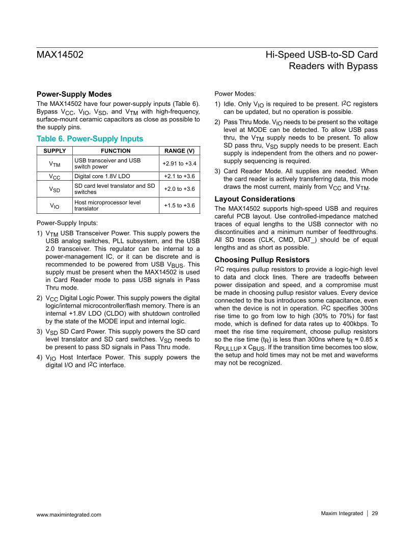
Power-Supply ModesThe MAX14502 have four power-supply inputs (Table 6). Bypass VCC, VIO, VSD, and VTM with high-frequency, surface-mount ceramic capacitors as close as possible to the supply pins.
Power-Supply Inputs:1) VTM USB Transceiver Power. This supply powers the
USB analog switches, PLL subsystem, and the USB 2.0 transceiver. This regulator can be internal to a power-management IC, or it can be discrete and is recommended to be powered from USB VBUS. This supply must be present when the MAX14502 is used in Card Reader mode to pass USB signals in Pass Thru mode.
2) VCC Digital Logic Power. This supply powers the digital logic/internal microcontroller/flash memory. There is an internal +1.8V LDO (CLDO) with shutdown controlled by the state of the MODE input and internal logic.
3) VSD SD Card Power. This supply powers the SD card level translator and SD card switches. VSD needs to be present to pass SD signals in Pass Thru mode.
4) VIO Host Interface Power. This supply powers the digital I/O and I2C interface.
Power Modes:1) Idle. Only VIO is required to be present. I2C registers
can be updated, but no operation is possible.2) Pass Thru Mode. VIO needs to be present so the voltage
level at MODE can be detected. To allow USB pass thru, the VTM supply needs to be present. To allow SD pass thru, VSD supply needs to be present. Each supply is independent from the others and no power-supply sequencing is required.
3) Card Reader Mode. All supplies are needed. When the card reader is actively transferring data, this mode draws the most current, mainly from VCC and VTM.
Layout ConsiderationsThe MAX14502 supports high-speed USB and requires careful PCB layout. Use controlled-impedance matched traces of equal lengths to the USB connector with no discontinuities and a minimum number of feedthroughs. All SD traces (CLK, CMD, DAT_) should be of equal lengths and as short as possible.
Choosing Pullup ResistorsI2C requires pullup resistors to provide a logic-high level to data and clock lines. There are tradeoffs between power dissipation and speed, and a compromise must be made in choosing pullup resistor values. Every device connected to the bus introduces some capacitance, even when the device is not in operation. I2C specifies 300ns rise time to go from low to high (30% to 70%) for fast mode, which is defined for data rates up to 400kbps. To meet the rise time requirement, choose pullup resistors so the rise time (tR) is less than 300ns where tR ≈ 0.85 x RPULLUP x CBUS. If the transition time becomes too slow, the setup and hold times may not be met and waveforms may not be recognized.
Table 6. Power-Supply InputsSUPPLY FUNCTION RANGE (V)
VTMUSB transceiver and USB switch power +2.91 to +3.4
VCC Digital core 1.8V LDO +2.1 to +3.6
VSDSD card level translator and SD switches +2.0 to +3.6
VIOHost microprocessor level translator +1.5 to +3.6
MAX14502 Hi-Speed USB-to-SD CardReaders with Bypass
www.maximintegrated.com Maxim Integrated 29
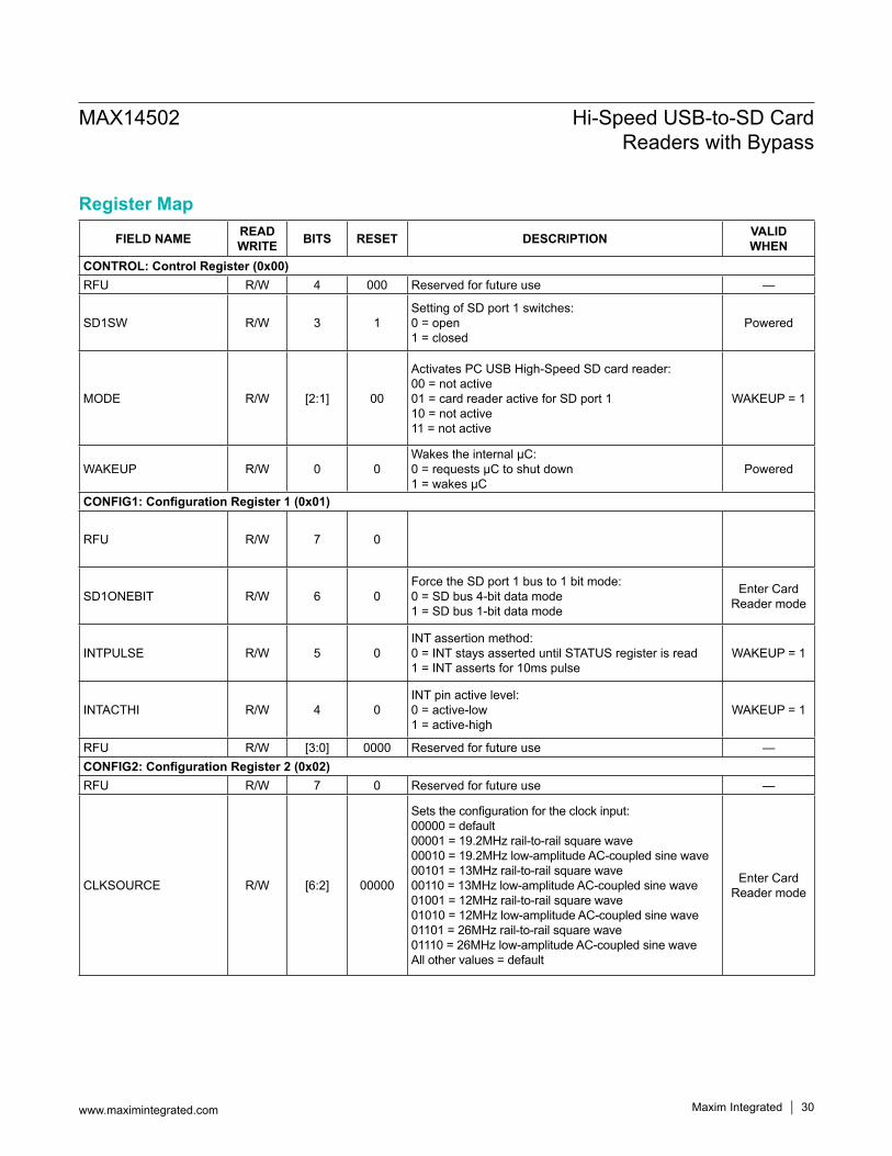
Register Map
FIELD NAME READ WRITE BITS RESET DESCRIPTION VALID
WHENCONTROL: Control Register (0x00)RFU R/W 4 000 Reserved for future use —
SD1SW R/W 3 1Setting of SD port 1 switches: 0 = open 1 = closed
Powered
MODE R/W [2:1] 00
Activates PC USB High-Speed SD card reader: 00 = not active 01 = card reader active for SD port 1 10 = not active 11 = not active
WAKEUP = 1
WAKEUP R/W 0 0Wakes the internal µC: 0 = requests µC to shut down 1 = wakes µC
Powered
CONFIG1: Configuration Register 1 (0x01)
RFU R/W 7 0
SD1ONEBIT R/W 6 0Force the SD port 1 bus to 1 bit mode: 0 = SD bus 4-bit data mode 1 = SD bus 1-bit data mode
Enter Card Reader mode
INTPULSE R/W 5 0INT assertion method: 0 = INT stays asserted until STATUS register is read 1 = INT asserts for 10ms pulse
WAKEUP = 1
INTACTHI R/W 4 0INT pin active level: 0 = active-low 1 = active-high
WAKEUP = 1
RFU R/W [3:0] 0000 Reserved for future use —CONFIG2: Configuration Register 2 (0x02)RFU R/W 7 0 Reserved for future use —
CLKSOURCE R/W [6:2] 00000
Sets the configuration for the clock input: 00000 = default 00001 = 19.2MHz rail-to-rail square wave 00010 = 19.2MHz low-amplitude AC-coupled sine wave 00101 = 13MHz rail-to-rail square wave 00110 = 13MHz low-amplitude AC-coupled sine wave 01001 = 12MHz rail-to-rail square wave 01010 = 12MHz low-amplitude AC-coupled sine wave 01101 = 26MHz rail-to-rail square wave 01110 = 26MHz low-amplitude AC-coupled sine wave All other values = default
Enter Card Reader mode
MAX14502 Hi-Speed USB-to-SD CardReaders with Bypass
www.maximintegrated.com Maxim Integrated 30
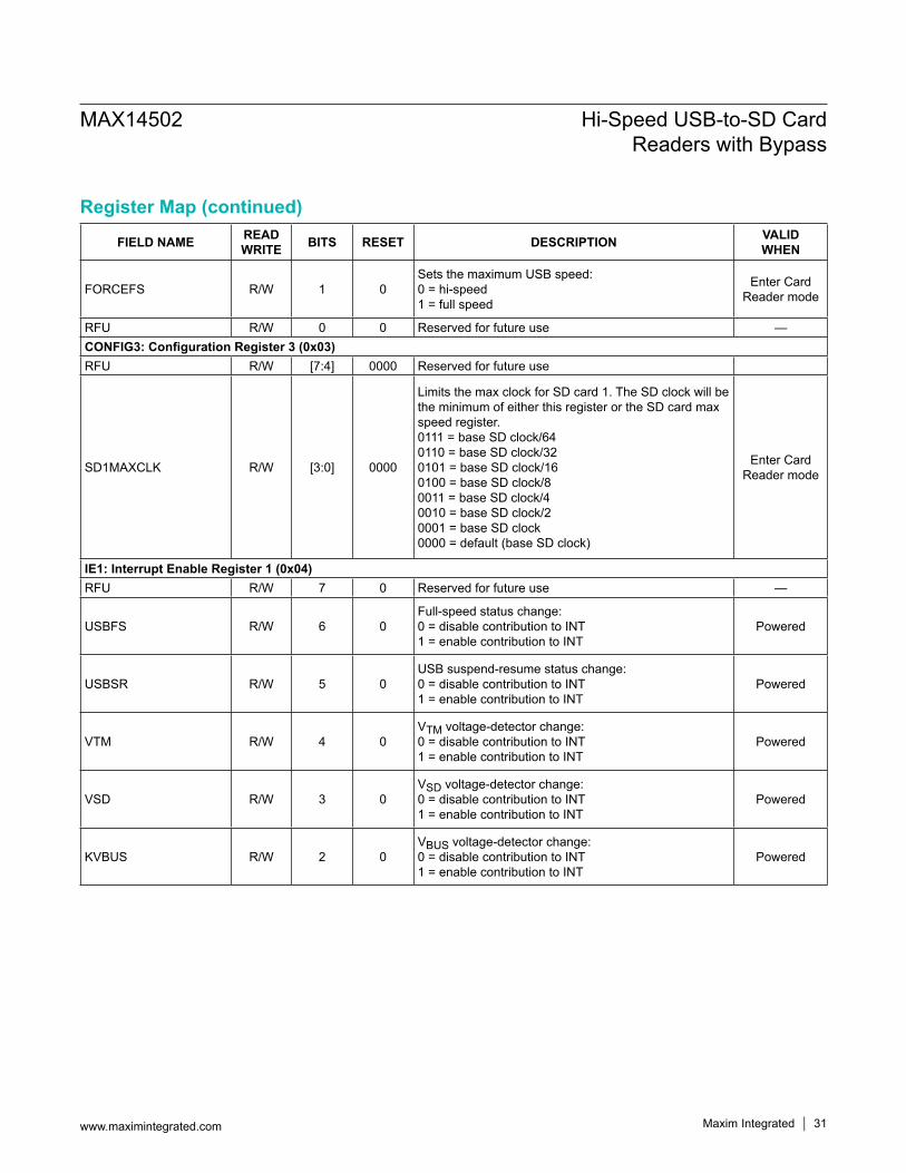
Register Map (continued)
FIELD NAME READ WRITE BITS RESET DESCRIPTION VALID
WHEN
FORCEFS R/W 1 0Sets the maximum USB speed: 0 = hi-speed 1 = full speed
Enter Card Reader mode
RFU R/W 0 0 Reserved for future use —CONFIG3: Configuration Register 3 (0x03)RFU R/W [7:4] 0000 Reserved for future use
SD1MAXCLK R/W [3:0] 0000
Limits the max clock for SD card 1. The SD clock will be the minimum of either this register or the SD card max speed register. 0111 = base SD clock/64 0110 = base SD clock/32 0101 = base SD clock/16 0100 = base SD clock/8 0011 = base SD clock/4 0010 = base SD clock/2 0001 = base SD clock 0000 = default (base SD clock)
Enter Card Reader mode
IE1: Interrupt Enable Register 1 (0x04)RFU R/W 7 0 Reserved for future use —
USBFS R/W 6 0Full-speed status change: 0 = disable contribution to INT 1 = enable contribution to INT
Powered
USBSR R/W 5 0USB suspend-resume status change: 0 = disable contribution to INT 1 = enable contribution to INT
Powered
VTM R/W 4 0VTM voltage-detector change: 0 = disable contribution to INT 1 = enable contribution to INT
Powered
VSD R/W 3 0VSD voltage-detector change: 0 = disable contribution to INT 1 = enable contribution to INT
Powered
KVBUS R/W 2 0VBUS voltage-detector change: 0 = disable contribution to INT 1 = enable contribution to INT
Powered
MAX14502 Hi-Speed USB-to-SD CardReaders with Bypass
www.maximintegrated.com Maxim Integrated 31

Register Map (continued)
FIELD NAME READ WRITE BITS RESET DESCRIPTION VALID
WHEN
BUSY R/W 1 0BUSY state change: 0 = disable contribution to INT 1 = enable contribution to INT
Powered
SDSTAT R/W 0 0
SD card status change: 0 = disable contribution to INT 1 = enable contribution to INT Note: Reflects currently selected card in Card Reader mode
Powered
IE2: Interrupt Enable Register 2 (0x05)
FWUPD R/W 7 0Firmware update status change: 0 = disable contribution to INT 1 = enable contribution to INT
Powered
RFU R/W [6:0] 0000000 Reserved for future use —USBVIDH: USB Vendor ID High Byte (0x06)
VID 1 R/W [7:0] 0x00
Bits 15–8 of USB vendor ID reported during card reader enumeration. If this register is written, the written value is used for USB enumeration, otherwise a default VID of 0x06BA (Maxim Integrated Products) is used.
Enter Card Reader mode
USBVIDL: USB Vendor ID Low Byte (0x07)
VID 2 R/W [7:0] 0x00
Bits 7–0 of USB vendor ID reported during card reader enumeration. If this register is written, the written value is used for USB enumeration, otherwise a default VID of 0x06BA (Maxim Integrated Products) is used.
Enter Card Reader mode
USBPIDH: USB Product ID High Byte (0x08)
PID 1 R/W [7:0] 0x00
Bits 15–8 of USB product ID reported during card reader enumeration. If this register is written, the written value is used for USB enumeration, otherwise a default PID of 0x38A4 is used.
Enter Card Reader mode
USBPIDL: USB Product ID Low Byte (0x09)
PID 2 R/W [7:0] 0x00
Bits 7–0 of USB product ID reported during card reader enumeration. If this register is written, the written value is used for USB enumeration, otherwise if zero, a default PID of 0x38A4 is used.
Enter Card Reader mode
Test Register (0x0A)Test Register R/W — 0x00 Do not write to this register —Test Register (0x0B)Test Register R/W — 0x00 Do not write to this register —Test Register (0x0C)Test Register R/W — 0x00 Do not write to this register —Test Register (0x0D)Test Register R/W — 0x00 Do not write to this register —
MAX14502 Hi-Speed USB-to-SD CardReaders with Bypass
www.maximintegrated.com Maxim Integrated 32

Register Map (continued)
FIELD NAME READ WRITE BITS RESET DESCRIPTION VALID
WHENTest Register (0x0E)Test Register R/W — 0x00 Do not write to this register —FWP: Firmware Portal (0x0F)Firmware Portal R/W [7:0] 0x00 Contact factory. Do not write to this register. —IRQ1: Interrupt Request Register 1 (0x10)RFU R 7 Reserved for future use —
USBFS R 6 0 = no change in USB full-speed mode status 1 = change in USB full-speed mode status
Enter Card Reader mode
USBSR R 5 0 = no change in USB suspend/resume status 1 = change in USB suspend/resume status
Enter Card Reader mode
VTM R 4 0 = no change in VTM detector status 1 = change in VTM detector status WAKEUP = 1
VSD R 3 0 = no change in VSD detector status 1 = change in VSD detector status WAKEUP = 1
VBUS R 2 0 = no change in VBUS detector status 1 = change in VBUS detector status WAKEUP = 1
BSY R 1 0 = no change in BUSY status 1 = change in BUSY status WAKEUP = 1
SDSTAT R 0 0 = no change in SD card present status 1 = change in SD card present status
Enter Card Reader mode
IRQ2: Interrupt Request Register 2 (0x11)
Firmware Update R 7 Contact factory Code download
RFU R [6:0] Reserved for future use —STATUS1: Status Register 1 (0x12)RFU R 7 Reserved for future use —
USBFS R 6 0 = no connection or Hi-Speed connection 1 = full-speed connection
Enter Card Reader mode
USBSR R 5 0 = USB resume 1 = USB suspend
Enter Card Reader mode
VTM R 4 0 = no voltage 1 = VTM supply present WAKEUP = 1
VSD R 3 0 = no voltage 1 = VSD supply present WAKEUP = 1
VBUS R 2 0 = no voltage 1 = VBUS supply present WAKEUP = 1
BSY R 1 0 = not busy 1 = busy WAKEUP = 1
MAX14502 Hi-Speed USB-to-SD CardReaders with Bypass
www.maximintegrated.com Maxim Integrated 33

FIELD NAME READ WRITE BITS RESET DESCRIPTION VALID
WHEN
SDSTAT R 0
The insert/removal status is only valid for the card currently set to Card Reader mode (Reg 0x00 bits 1-2) 0 = no card 1 = card present
Enter Card Reader mode
STATUS2: Status Register 2 (0x13)RFU R [7:0] Reserved for future use —FWUGRRH: Firmware Upgrade Response Data High Byte (0x14)High Byte of Response Data R [7:0] Contact factory Code
downloadFWUPGRL: Firmware Upgrade Response Data Low Byte (0x15)Low Byte of Response Data R [7:0] Contact factory Code
downloadRFU Register (0x16)RFU R [7:0] Reserved for future use —RFU Register (0x17)RFU R [7:0] Reserved for future use —RFU Register (0x18)RFU R [7:0] Reserved for future use —RFU Register (0x19)RFU R [7:0] Reserved for future use —RFU Register (0x1A)RFU R [7:0] Reserved for future use —Firmware Incremental Revision (0x1B)Firmware Incremental Revision R [7:0] Firmware incremental revision WAKEUP = 1
Firmware Minor Revision (0x1C)Firmware Minor Revision R [7:0] Firmware minor revision WAKEUP = 1Firmware Major Revision (0x1D)Firmware Major Revision R [7:0] Firmware major revision WAKEUP = 1Chip Revision (0x1E)Chip Revision R [7:0] Chip revision WAKEUP = 1Package Type (0x1F)
Package Type R [7:0] 0x00 = 40-lead TQFN 0xFF = unknown WAKEUP = 1
Register Map (continued)
MAX14502 Hi-Speed USB-to-SD CardReaders with Bypass
www.maximintegrated.com Maxim Integrated 34

Functional Diagram
VSD VIO
CD+
HOST PROCESSOR
USB SWITCHES
CD-
D+
D-
VBUS
HD+
HD-
D+
D-
USBCONNECTOR
SD CARD INTERFACE LEVEL TRANSLATORS
1.8VLDO
VBUSDET
MICROCONTROLLER
FLASH
PLL48/52MHz
SQR TCXO
SRAM
USB SIE
OSC
ROM
I/O LEVEL TRANSLATORS
HOST INTERFACE
USB 2.0TRANSCEIVER
CCRD_PRST
CCLK 1
CCMD 1
HCRD_PRST
HCLK1
HCMD1
CDAT 1_0
CDAT 1_1
CDAT 1_2
SD_DETECT
CLK
CMD
DAT 0
DAT 1
DAT 2
HDAT 1_0
HDAT 1_1
HDAT 1_2
SD_DETECT
CLK
CMD
DAT 0
DAT 1
DAT 2
SD PORT1
SD SLOT
SD CARD
SD PORT 1 SWITCHES
CDAT 1_3
CLDO
VCC
DAT 3 HDAT 1_3
MODE
BUSY
BERR/INT
USB
SCL
SDA
RST
ADD
I2C_SEL
FREF
DAT 3
1µF
0.1µF
VSD
VCC
VTM(+2.91V TO +3.4V)
VIO
VIO
MAX14502
KVBUS
RREF
1µF
0.1µF
1µF
6.19kΩ1%
1.5kΩ
VTM
MAX14502 Hi-Speed USB-to-SD CardReaders with Bypass
www.maximintegrated.com Maxim Integrated 35
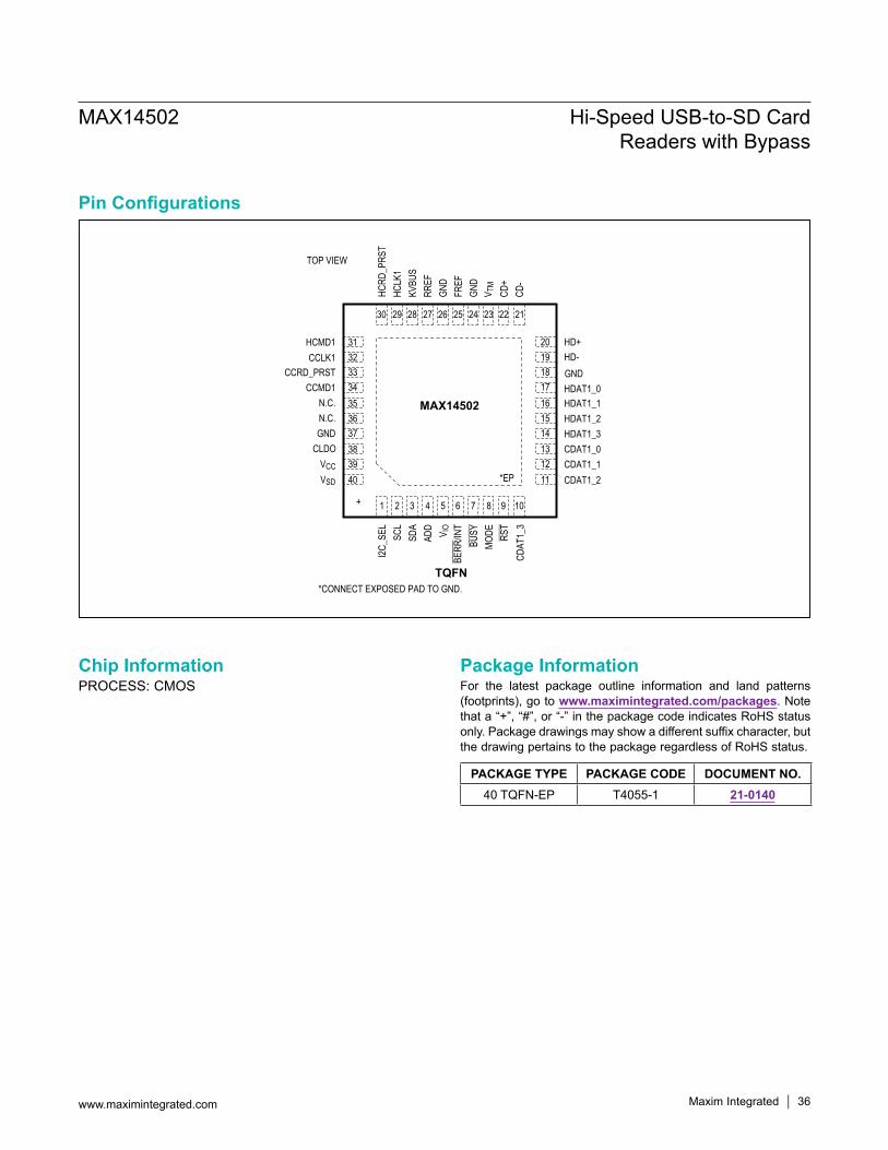
Package InformationFor the latest package outline information and land patterns (footprints), go to www.maximintegrated.com/packages. Note that a “+”, “#”, or “-” in the package code indicates RoHS status only. Package drawings may show a different suffix character, but the drawing pertains to the package regardless of RoHS status.
Chip InformationPROCESS: CMOS
Pin Configurations
HCRD
_PRS
THC
LK1
RREF
GND
V TM
CD+
CD-
FREF
GND
KVBU
SSD
AAD
D V IO
BUSY
MODE RS
TCD
AT1_
3
SCL
I2C_S
EL
HDAT1_2HDAT1_1HDAT1_0
HD-HD+
HDAT1_3CDAT1_0CDAT1_1CDAT1_2
VCC
CLDOGNDN.C.N.C.
CCMD1CCRD_PRST
CCLK1HCMD1
VSD
TQFN
MAX14502
TOP VIEW
BERR
/INT
GND
1 2 3 4 5 6 7 8 9 10
40 39 38 37 36 35 34 33 32 31
11 *EP 12 13 14 15 16 17 18 19 20
30 29 28 27 26 25 24 23 22 21
+
*CONNECT EXPOSED PAD TO GND.
PACKAGE TYPE PACKAGE CODE DOCUMENT NO.40 TQFN-EP T4055-1 21-0140
MAX14502 Hi-Speed USB-to-SD CardReaders with Bypass
www.maximintegrated.com Maxim Integrated 36

Revision HistoryREVISION NUMBER
REVISION DATE DESCRIPTION PAGES
CHANGED
0 4/08 Initial release —
1 4/09 Fixed data sheet to reflect new rev material including EC table, Pin Description, Applications Information, Functional Diagram, and Pin Configurations 1–41
2 4/16 Future products (MAX14500, MAX14501, MAX14503) removed from data sheet 1-41
3 6/16 Removed WLP package from data sheet. 1–39
Maxim Integrated cannot assume responsibility for use of any circuitry other than circuitry entirely embodied in a Maxim Integrated product. No circuit patent licenses are implied. Maxim Integrated reserves the right to change the circuitry and specifications without notice at any time. The parametric values (min and max limits) shown in the Electrical Characteristics table are guaranteed. Other parametric values quoted in this data sheet are provided for guidance.
Maxim Integrated and the Maxim Integrated logo are trademarks of Maxim Integrated Products, Inc. © 2016 Maxim Integrated Products, Inc. 37
MAX14502 Hi-Speed USB-to-SD Card Readers with Bypass
For pricing, delivery, and ordering information, please contact Maxim Direct at 1-888-629-4642, or visit Maxim Integrated’s website at www.maximintegrated.com.