max15026 low-cost, small, 4.5v to 28v wide … max15026 low-cost, small, 4.5v to 28v wide operating...
TRANSCRIPT

MAX15026
Low-Cost, Small, 4.5V to 28V Wide OperatingRange, DC-DC Synchronous Buck Controller
EVALUATION KIT AVAILABLE
19-4108; Rev 5; 11/12
For pricing, delivery, and ordering information, please contact Maxim Directat 1-888-629-4642, or visit Maxim’s website at www.maximintegrated.com.
General DescriptionThe MAX15026 synchronous step-down controller oper-ates from a 4.5V to 28V input voltage range and gener-ates an adjustable output voltage from 85% of the inputvoltage down to 0.6V while supporting loads up to 25A.The device allows monotonic startup into a prebiasedbus without discharging the output and features adap-tive internal digital soft-start.
The MAX15026 offers the ability to adjust the switchingfrequency from 200kHz to 2MHz with an external resis-tor. The MAX15026’s adaptive synchronous rectificationeliminates the need for an external freewheelingSchottky diode. The device also utilizes the externallow-side MOSFET’s on-resistance as a current-senseelement, eliminating the need for a current-sense resis-tor. This protects the DC-DC components from damageduring output overloaded conditions or output short-circuit faults without requiring a current-sense resistor.Hiccup-mode current limit reduces power dissipationduring short-circuit conditions. The MAX15026 includesa power-good output and an enable input with preciseturn-on/turn-off threshold, which can be used for inputsupply monitoring and for power sequencing.
Additional protection features include sink-mode cur-rent limit and thermal shutdown.
Sink-mode current limit prevents reverse inductor cur-rent from reaching dangerous levels when the device issinking current from the output.
The MAX15026 is available in a space-saving and ther-mally enhanced 3mm x 3mm, 14-pin TDFN-EP pack-age. The MAX15026 operates over the extended -40°Cto +85°C and automotive -40°C to +125°C temperatureranges.
The MAX15026C is designed to provide additional mar-gin for break-before-make times.
The MAX15026B/MAX15026C provide a soft-stop feature to ramp down the output voltage at turn-off. Thesoft-stop function is disabled in the MAX15026D.
ApplicationsSet-Top Boxes
LCD TV Secondary Supplies
Switches/Routers
Power Modules
DSP Power Supplies
Points-of-Load Regulators
Features 4.5V to 28V or 5V ±10% Input Supply Range 0.6V to (0.85 x VIN) Adjustable Output Adjustable 200kHz to 2MHz Switching Frequency Ability to Start into a Prebiased Load Lossless, Cycle-by-Cycle Valley Mode Current
Limit with Adjustable, Temperature-CompensatedThreshold
Sink-Mode Current-Limit Protection Adaptive Internal Digital Soft-Start ±1% Accurate Voltage Reference Internal Boost Diode Adaptive Synchronous Rectification Eliminates
External Freewheeling Schottky Diode Hiccup-Mode Short-Circuit Protection Thermal Shutdown Power-Good Output and Enable Input for Power
Sequencing ±5% Accurate Enable Input Threshold AEC-Q100 Qualified (MAX15026B)
2
4
5
*EP
13
11
10
LX
DL
DRV
VCC
EN
LIM
MAX15026
1 + 14 DHIN
3 12 BSTPGOOD
6 9 GNDCOMP
7 8 RTFB
TDFN(3mm x 3mm)
TOP VIEW
*EP = EXPOSED PAD.
Pin Configuration
Ordering InformationPART TEMP RANGE PIN-PACKAGE
MAX15026BETD+ -40°C to +85°C 14 TDFN-EP*
MAX15026BETD/V+T -40°C to +85°C 14 TDFN-EP*
MAX15026CETD+ -40°C to +85°C 14 TDFN-EP*
MAX15026BATD+ -40°C to +125°C 14 TDFN-EP*
MAX15026CATD+ -40°C to +125°C 14 TDFN-EP*
MAX15026DATD+ -40°C to +125°C 14 TDFN-EP*+Denotes a lead(Pb)-free/RoHS-compliant package.*EP = Exposed pad. T = Tape and reel./V denotes an automotive qualified part.MAX15026D recommended for new designs.

MAX15026Low-Cost, Small, 4.5V to 28V Wide OperatingRange, DC-DC Synchronous Buck Controller
2 Maxim Integrated
ABSOLUTE MAXIMUM RATINGS
ELECTRICAL CHARACTERISTICS(VIN = 12V, RRT = 27kΩ, RLIM = 30kΩ, CVCC = 4.7µF, CIN = 1µF, TA = -40°C to +85°C (MAX15026B/CETD+, MAX15026BETD/V+), TA = TJ = -40°C to +125°C (MAX15026B/C/DATD+), unless otherwise noted. Typical values are at TA = +25°C.) (Note 2)
Stresses beyond those listed under “Absolute Maximum Ratings” may cause permanent damage to the device. These are stress ratings only, and functionaloperation of the device at these or any other conditions beyond those indicated in the operational sections of the specifications is not implied. Exposure toabsolute maximum rating conditions for extended periods may affect device reliability.
Note 1: Dissipation wattage values are based on still air with no heatsink. Actual maximum power dissipation is a function of heatextraction technique and may be substantially higher. Package thermal resistances were obtained using the methoddescribed in JEDEC specification JESD51-7, using a four-layer board. For detailed information on package thermal consid-erations, refer to www.maximintegrated.com/thermal-tutorial.
IN to GND...............................................................-0.3V to +30VBST to GND............................................................-0.3V to +36VLX to GND .................................................................-1V to +30VEN to GND................................................................-0.3V to +6VPGOOD to GND .....................................................-0.3V to +30VBST to LX..................................................................-0.3V to +6VDH to LX ...............................................….-0.3V to (VBST + 0.3V)DRV to GND .............................................................-0.3V to +6VDL to GND ................................................-0.3V to (VDRV + 0.3V)VCC to GND...............-0.3V to the lower of +6V and (VIN + 0.3V)All Other Pins to GND.................................-0.3V to (VCC + 0.3V)VCC Short Circuit to GND...........................................Continuous
DRV Input Current.............................................................600mAPGOOD Sink Current ............................................................5mAContinuous Power Dissipation (TA = +70°C) (Note 1)
14-Pin TDFN-EP, Multilayer Board(derate 24.4mW/°C above +70°C)..............................1951mW
Operating Temperature Range MAX15026B/CETD+, MAX15026BETD/V+.......-40°C to +85°CMAX15026B/C/DATD+ ...................................-40°C to +125°C
Junction Temperature ......................................................+150°CStorage Temperature Range .............................-60°C to +150°CLead Temperature (soldering, 10s) .................................+300°CSoldering Temperature (reflow) .......................................+260°C
PARAMETER SYMBOL CONDITIONS MIN TYP MAX UNITS
GENERAL
4.5 28Input Voltage Range VIN
VIN = VCC = VDRV 4.5 5.5V
Quiescent Supply Current VFB = 0.9V, no switching 1.75 2.75 mA
Shutdown Supply Current IIN_SBY EN = GND 290 500 µA
Enable to Output Delay 480 µs
VCC High to Output Delay EN = VCC 375 µs
VCC REGULATOR
6V < VIN < 28V, ILOAD = 25mAOutput Voltage VCC
VIN = 12V, 1mA < ILOAD < 70mA5.0 5.25 5.5 V
VCC Regulator Dropout VIN = 4.5V, ILOAD = 70mA 0.28 V
VCC Short-Circuit Output Current VIN = 5V 100 200 300 mA
VCC Undervoltage Lockout VCC_UVLO VCC rising 3.8 4.0 4.2 V
VCC Undervoltage LockoutHysteresis
400 mV
ERROR AMPLIFIER (FB, COMP)
FB Input Voltage Set-Point VFB 585 591 597 mV
FB Input Bias Current IFB VFB = 0.6V -250 +250 nA
FB to COMP Transconductance gM ICOMP = ±20µA 600 1200 1800 µS
Amplifier Open-Loop Gain 80 dB
Amplifier Unity-Gain Bandwidth Capacitor from COMP to GND = 50pF 4 MHz
VCOMP-RAMP Minimum Voltage 160 mV
COMP Source/Sink Current ICOMP VCOMP = 1.4V 50 80 110 µA

MAX15026Low-Cost, Small, 4.5V to 28V Wide Operating
Range, DC-DC Synchronous Buck Controller
3Maxim Integrated
PARAMETER SYMBOL CONDITIONS MIN TYP MAX UNITS
ENABLE (EN)
EN Input High VEN_H VEN rising 1.14 1.20 1.26 V
EN Input Low VEN_L VEN falling 0.997 1.05 1.103 V
EN Input Leakage Current ILEAK_EN VEN = 5.5V -1 +1 µA
OSCILLATOR
Switching Frequency fSW RRT = 27kΩ 540 600 660 kHz
1MHz Switching Frequency RRT = 15.7kΩ 0.9 1 1.1 MHz
2MHz Switching Frequency RRT = 7.2kΩ 1.8 2.0 2.4 MHz
Switching Frequency AdjustmentRange (Note 3)
200 2000 kHz
RT Voltage VRT 1.19 1.205 1.22 V
PWM Ramp Peak-to-PeakAmplitude
VRAMP 1.8 V
PWM Ramp Valley VVALLEY 0.8 V
Minimum Controllable On-Time 65 100 ns
Maximum Duty Cycle fSW = 600kHz 85 88 %
Minimum Low-Side On-Time RRT = 15.7kΩ 75 110 150 ns
OUTPUT DRIVERS/DRIVER SUPPLY (DRV)
DRV Undervoltage Lockout VDRV_UVLO VDRV rising 4.0 4.2 4.4 V
DRV Undervoltage LockoutHysteresis
400 mV
Low, sinking 100mA, VBST = 5V 1 3DH On-Resistance
High, sourcing 100mA, VBST = 5V 1.5 4.5Ω
Low, sinking 100mA, VBST = 5.2V 1 3DL On-Resistance
High, sourcing 100mA, VBST = 5.2V 1.5 4.5Ω
Sinking 4DH Peak Current CLOAD = 10nF
Sourcing 3A
Sinking 4DL Peak Current CLOAD = 10nF
Sourcing 3A
DH/DL Break-Before-Make Time DH at 1V (falling) to DL at 1V (rising) 10 (18, Note 5) ns
DL/DH Break-Before-Make Time DL at 1V (falling) to DH at 1V (rising) 10 (20, Note 6) ns
SOFT-START
Soft-Start Duration 2048Switching
Cycles
Reference Voltage Steps 64 Steps
CURRENT LIMIT/HICCUP
Current-Limit ThresholdAdjustment Range
Cycle-by-cycle valley current-limitthreshold adjustment rangevalley limit = VLIM/10
30 300 mV
ELECTRICAL CHARACTERISTICS (continued)(VIN = 12V, RRT = 27kΩ, RLIM = 30kΩ, CVCC = 4.7µF, CIN = 1µF, TA = -40°C to +85°C (MAX15026B/CETD+, MAX15026BETD/V+), TA = TJ = -40°C to +125°C (MAX15026B/C/DATD+), unless otherwise noted. Typical values are at TA = +25°C.) (Note 2)

MAX15026Low-Cost, Small, 4.5V to 28V Wide OperatingRange, DC-DC Synchronous Buck Controller
4 Maxim Integrated
PARAMETER SYMBOL CONDITIONS MIN TYP MAX UNITS
LIM Reference Current ILIM VLIM = 0.3V to 3V (Note 4) 45 50 55 µA
LIM Reference Current Tempco VLIM = 0.3V to 3V 2300 ppm/°C
Number of Consecutive Current-Limit Events to Hiccup
7 Events
Soft-Start Timeout 4096Switching
Cycles
Soft-Start Restart Timeout 8192Switching
Cycles
Hiccup Timeout Out of soft-start 4096Switching
Cycles
Peak Low-Side Sink CurrentLimit
Sink limit = 1.5V, RLIM = 30kΩ (Note 4) 75 mV
BOOST
Boost Switch Resistance VIN = VCC = 5V, IBST = 10mA 3 8 Ω
POWER-GOOD OUTPUT
PGOOD Threshold Rising 90 94.5 97.5 % VFB
PGOOD Threshold Falling 88 92 94.5 %VFB
PGOOD Output Leakage ILEAK_PGD VIN = VPGOOD = 28V, VEN = 5V, VFB = 1V -1 +1 µA
PGOOD Output Low Voltage VPGOOD_L IPGOOD = 2mA, EN = GND 0.4 V
THERMAL SHUTDOWN
Thermal-Shutdown Threshold Temperature rising +150 °C
Thermal-Shutdown Hysteresis Temperature falling 20 °C
ELECTRICAL CHARACTERISTICS (continued)(VIN = 12V, RRT = 27kΩ, RLIM = 30kΩ, CVCC = 4.7µF, CIN = 1µF, TA = -40°C to +85°C (MAX15026B/CETD+, MAX15026BETD/V+), TA = TJ = -40°C to +125°C (MAX15026B/C/DATD+), unless otherwise noted. Typical values are at TA = +25°C.) (Note 2)
Note 2: All devices are 100% tested at room temperature and guaranteed by design over the specified temperature range.
Note 3: Select RRT as: where fSW is in Hertz.
Note 4: TA = +25°C.Note 5: 10ns for MAX15026B, 18ns for the MAX15026C/D.Note 6: 10ns for MAX15026B, 20ns for the MAX15026C/D.
R17.3 10
f 1x10 )x(fRT
9
SW7
SW= ×
+ −( )2

EFFICIENCY vs. LOAD CURRENT (MAX15026B/C)
MAX
1502
6 to
c01
LOAD CURRENT (A)
EFFI
CIEN
CY (%
)
8 1062 4
10
20
30
40
50
60
70
80
90
100
00 12
VOUT = 3.3VVOUT = 1.2V
VOUT = 5V
VOUT = 1.8V
EFFICIENCY vs. LOAD CURRENT(VIN = 12V, VCC = VDRV = 5V)
MAX
1502
6 to
c02
LOAD CURRENT (A)
EFFI
CIEN
CY (%
)
106 8420 12
VOUT = 3.3VVOUT = 1.2V
VOUT = 5V
VOUT = 1.8V
10
20
30
40
50
60
70
80
90
100
0
VOUT vs. LOAD CURRENT
MAX
1502
6 to
c03
LOAD CURRENT (A)
% O
UTPU
T FR
OM N
OMIN
AL
106 8420 12
-0.9
-0.8
-0.7
-0.6
-0.5
-0.4
-0.3
-0.2
-0.1
0
-1.0
VCC vs. LOAD CURRENT
MAX
1502
6 to
c04
LOAD CURRENT (mA)
V CC
(V)
8020 40 60
5.230
5.235
5.240
5.245
5.250
5.255
5.260
5.265
5.2250 100
VCC LINE REGULATIONM
AX15
026
toc0
5
VIN (V)
V CC
(V)
252015105
4.4
4.5
4.6
4.7
4.8
4.9
5.0
5.1
5.2
5.3
4.30 30
5mA
50mA
VCC vs. TEMPERATURE
MAX
1502
6 to
c06
TEMPERATURE (°C)
V CC
(V)
603510-15
5.238
5.240
5.242
5.244
5.246
5.248
5.236-40 85
SWITCHING FREQUENCYvs. RESISTANCE
MAX
1502
6 to
c07
RESISTANCE (kΩ)
SW
ITCH
ING
FREQ
UENC
Y (k
Hz)
80604020
500
1000
1500
2000
2500
00 100
SWITCHING FREQUENCYvs. TEMPERATURE
MAX
1502
6 to
c08
TEMPERATURE (°C)
SW
ITCH
ING
FREQ
UENC
Y (k
Hz)
603510-15
500
1000
1500
2000
2500
0-40 85
RRT = 7.2kΩ
RRT = 15.7kΩ
RRT = 27kΩRRT = 85kΩ
SUPPLY CURRENTvs. SWITCHING FREQUENCY
MAX
1502
6 to
c09
SWITCHING FREQUENCY (kHz)
SUPP
LY C
URRE
NT (m
A)
1000
10
20
30
40
50
60
70
80
90
0100 10,000
Typical Operating Characteristics(VIN = 12V, TA = +25°C. The following TOCs are for MAX15026B/C/D, unless otherwise noted.) (See the circuit of Figure 5.)
MAX15026Low-Cost, Small, 4.5V to 28V Wide Operating
Range, DC-DC Synchronous Buck Controller
5Maxim Integrated

Typical Operating Characteristics (continued)(VIN = 12V, TA = +25°C. The following TOCs are for MAX15026B/C/D, unless otherwise noted.) (See the circuit of Figure 5.)
LIM REFERENCE CURRENTvs. TEMPERATURE
MAX
1502
6 to
c10
TEMPERATURE (°C)
LIM
REF
EREN
CE C
URRE
NT (µ
A)
603510-15
10
20
30
40
50
60
70
0-40 85
SINK AND SOURCE CURRENT-LIMITTHRESHOLDS vs. RESISTANCE (RILIM)
MAX
1502
6 to
c11
RESISTANCE (kΩ)
CURR
ENT-
LIM
IT T
HRES
HOLD
S (V
)
605040302010
-0.3
-0.2
-0.1
0
0.1
0.2
-0.40 70
SINK CURRENT-LIMIT
SOURCE CURRENT-LIMIT
LOAD TRANSIENT ON OUTMAX15026 toc12
400µs/div
AC-COUPLEDVOUT200mV/div
IOUT
10A
1A
STARTUP AND DISABLE FROM EN(RLOAD = 1.5Ω)
MAX15026 toc13
4ms/div
VOUT1V/div
VIN5V/div
PGOOD5V/div
STARTUP RISE TIME(MAX15026B)
MAX15026 toc14
1ms/div
VIN5V/div
VOUT1V/div
POWER-DOWN FALL TIMEMAX15026 toc15
4ms/div
VIN5V/div
VOUT1V/div
STARTUP RISE TIME(MAX15026C/D)
MAX15026 toc16
1ms/div
VIN5V/div
VOUT1V/div0V OUTPUT
SOFT-START WITH 0.5V PREBIAS AT NO LOAD (MAX15026C/D)
MAX15026 toc17
1ms/div
VIN5V/div
VOUT1V/div
0.5V OUTPUT PREBIAS
OUTPUT SHORT-CIRCUIT BEHAVIOR MONITOROUTPUT VOLTAGE AND CURRENT
MAX15026 toc18
4ms/div
500mV/div
0VOUT
IOUT
20A/div
0
MAX15026Low-Cost, Small, 4.5V to 28V Wide OperatingRange, DC-DC Synchronous Buck Controller
6 Maxim Integrated

Pin Description
PIN NAME FUNCTION
1 INRegulator Input. Bypass IN to GND with a 1µF minimum ceramic capacitor. Connect IN to VCC whenoperating in the 5V ±10% range.
2 VCC
5.25V Linear Regulator Output. Bypass VCC to GND with a minimum of 4.7µF low-ESR ceramiccapacitor to ensure stability up to the regulated rated current when VCC supplies the drive current atDRV. Bypass VCC to GND when VCC supplies the device core quiescent current with a 2.2µFminimum ceramic capacitor.
3 PGOOD Open-Drain Power-Good Output. Connect PGOOD with an external resistor to any supply voltage.
4 ENActive-High Enable Input. Pull EN to GND to disable the output. Connect EN to VCC for always-onoperation. EN can be used for power sequencing and as a UVLO adjustment input.
5 LIMCurrent-Limit Adjustment. Connect a resistor from LIM to GND to adjust current-limit threshold from30mV (RLIM = 6kΩ) to 300mV (RLIM = 60kΩ). See the Setting the Valley Current Limit section.
6 COMPCompensation Input. Connect compensation network from COMP to FB or from COMP to GND. Seethe Compensation section.
7 FBFeedback Input. Connect FB to a resistive divider between output and GND to adjust the outputvoltage between 0.6V and (0.85 x Input Voltage). See the Setting the Output Voltage section.
8 RTOscillator Timing Resistor Input. Connect a resistor from RT to GND to set the oscillator frequencyfrom 200kHz to 2MHz. See the Setting the Switching Frequency section.
9 GND Ground
10 DRVDrive Supply Voltage. DRV is internally connected to the anode terminal of the internal boost diode.Bypass DRV to GND with a 2.2µF minimum ceramic capacitor (see the Typical Application Circuits).
11 DL Low-Side Gate-Driver Output. DL swings from DRV to GND. DL is low during UVLO.
12 BSTBoost Flying Capacitor. Connect a ceramic capacitor with a minimum value of 100nF between BSTand LX.
13 LXExternal Inductor Connection. Connect LX to the switching side of the inductor. LX serves as thelower supply rail for the high-side gate driver and as a sensing input of the drain to source voltagedrop of the synchronous MOSFET.
14 DH High-Side Gate-Driver Output. DH swings from LX to BST. DH is low during UVLO.
— EPExposed Pad. Internally connected to GND. Connect EP to a large copper plane at GND potential toimprove thermal dissipation. Do not use EP as the only GND ground connection.
MAX15026Low-Cost, Small, 4.5V to 28V Wide Operating
Range, DC-DC Synchronous Buck Controller
7Maxim Integrated

MAX15026Low-Cost, Small, 4.5V to 28V Wide OperatingRange, DC-DC Synchronous Buck Controller
8 Maxim Integrated
Functional Diagram
OSCILLATOR
DC-DCAND
OSCILLATORENABLELOGIC
VREF
RT
EN
ENABLE COMPARATOR
OSC_ENABLE
BANDGAPOK
GENERATOR
VCCUVLO
DRVUVLO
THERMALSHUTDOWN
AND ILIMCURRENT
GEN
INUVLO
BGAP_OK
BGAP_OK
EN_INT
VL_OK
VDRV_OK
SHUTDOWN
VIN_OK
VREF
VIN_OK
VIN_OK
IBIAS
VBGAP
BGAP_OK
BGAP_OK
VDRV
VIN_OK
VBGAP
LIM
IN
VCC
INTERNALVOLTAGE
REGULATOR
MAINBIAS
CURRENTGENERATOR
VREF = 0.6V
VBGAP = 1.24V
BANDGAPREFERENCE
CK
ENABLE
gMSOFT-START/ SOFT-STOP LOGIC AND
HICCUP LOGIC
VREF
HICCUP
CK
ENABLE DH_DL_ENABLE
VREF
VREF
CK
CKDH_DL_ENABLE
HICCUPTIMEOUT
FB1
DAC_VREF
PWMCOMPARATOR
RAMPGENERATOR
SINKCURRENT-LIMITCOMPARATOR
PGOODCOMPARATOR
VALLEYCURRENT-LIMITCOMPARATOR
PWM
PWMCONTROL
LOGIC
BOOSTDRIVER
HIGH-SIDE
DRIVER
LOW-SIDE
DRIVER
RAMP
GATEP
HICCUP TIMEOUT
HICCUP
LIM/20
LIM/10
COMP
BST
DH
LX
DRV
DL
GND
FB
PGOOD
GND
MAX15026

MAX15026Low-Cost, Small, 4.5V to 28V Wide Operating
Range, DC-DC Synchronous Buck Controller
9Maxim Integrated
Detailed DescriptionThe MAX15026 synchronous step-down controller oper-ates from a 4.5V to 28V input voltage range and gener-ates an adjustable output voltage from 85% of the inputvoltage down to 0.6V while supporting loads up to 25A.As long as the device supply voltage is within 5.0V to5.5V, the input power bus (VIN) can be as low as 3.3V.
The MAX15026 offers adjustable switching frequencyfrom 200kHz to 2MHz with an external resistor. Theadjustable switching frequency provides design flexi-bility in selecting passive components. The MAX15026adopts an adaptive synchronous rectification to elimi-nate an external freewheeling Schottky diode andimprove efficiency. The device utilizes the on-resis-tance of the external low-side MOSFET as a current-sense element. The current-limit threshold voltage isresistor-adjustable from 30mV to 300mV and is temper-ature-compensated, so that the effects of the MOSFETRDS(ON) variation over temperature are reduced. Thiscurrent-sensing scheme protects the external compo-nents from damage during output overloaded condi-tions or output short-circuit faults without requiring acurrent-sense resistor. Hiccup-mode current limitreduces power dissipation during short-circuit condi-tions. The MAX15026 includes a power-good outputand an enable input with precise turn-on/-off thresholdto be used for monitoring and for power sequencing.
The MAX15026 features internal digital soft-start thatallows prebias startup without discharging the output.The digital soft-start function employs sink current limit-ing to prevent the regulator from sinking excessive cur-rent when the prebias voltage exceeds theprogrammed steady-state regulation level. The digitalsoft-start feature prevents the synchronous rectifierMOSFET and the body diode of the high-side MOSFETfrom experiencing dangerous levels of current while theregulator is sinking current from the output. TheMAX15026 shuts down at a junction temperature of+150°C to prevent damage to the device.
DC-DC PWM ControllerThe MAX15026 step-down controller uses a PWM volt-age-mode control scheme (see the Functional Diagram).Control-loop compensation is external for providing max-imum flexibility in choosing the operating frequency andoutput LC filter components. An internal transconduc-tance error amplifier produces an integrated error volt-age at COMP that helps to provide higher DC accuracy.The voltage at COMP sets the duty cycle using a PWMcomparator and a ramp generator. On the rising edge ofan internal clock, the high-side n-channel MOSFET turnson and remains on until either the appropriate duty cycle
or the maximum duty cycle is reached. During the on-time of the high-side MOSFET, the inductor currentramps up. During the second-half of the switching cycle,the high-side MOSFET turns off and the low-side n-chan-nel MOSFET turns on. The inductor releases the storedenergy as the inductor current ramps down, providingcurrent to the output. Under overload conditions, whenthe inductor current exceeds the selected valley current-limit threshold (see the Current-Limit Circuit (LIM) sec-tion), the high-side MOSFET does not turn on at thesubsequent clock rising edge and the low-side MOSFETremains on to let the inductor current ramp down.
Internal 5.25V Linear RegulatorAn internal linear regulator (VCC) provides a 5.25V nomi-nal supply to power the internal functions and to drivethe low-side MOSFET. Connect IN and VCC togetherwhen using an external 5V ±10% power supply. Themaximum regulator input voltage (VIN) is 28V. Bypass INto GND with a 1µF ceramic capacitor. Bypass the outputof the linear regulator (VCC) with a 4.7µF ceramic capac-itor to GND. The VCC dropout voltage is typically 125mV.When VIN is higher than 5.5V, VCC is typically 5.25V. TheMAX15026 also employs an undervoltage lockout circuitthat disables the internal linear regulator when VCC fallsbelow 3.6V (typ). The 400mV UVLO hysteresis preventschattering on power-up/power-down.
The internal VCC linear regulator can source up to70mA to supply the IC, power the low-side gate driver,recharge the external boost capacitor, and supply smallexternal loads. The current available for external loadsdepends on the current consumed by the MOSFETgate drivers.
For example, when switching at 600kHz, a MOSFETwith 18nC total gate charge (at VGS = 5V) requires(18nC x 600kHz) = 11mA. The internal control functionsconsume 5mA maximum. The current available forexternal loads is:
(70 – (2 x 11) – 5)mA ≅ 43mA
MOSFET Gate Drivers (DH, DL)DH and DL are optimized for driving large-size n-chan-nel power MOSFETs. Under normal operating condi-tions and after startup, the DL low-side drive waveformis always the complement of the DH high-side drivewaveform, with controlled dead-time to prevent cross-conduction or shoot-through. An adaptive dead-timecircuit monitors the DH and DL outputs and preventsthe opposite-side MOSFET from turning on until theother MOSFET is fully off. Thus, the circuit allows thehigh-side driver to turn on only when the DL gate driverhas turned off, preventing the low-side (DL) from turn-ing on until the DH gate driver has turned off.

MAX15026Low-Cost, Small, 4.5V to 28V Wide OperatingRange, DC-DC Synchronous Buck Controller
10 Maxim Integrated
The adaptive driver dead-time allows operation withoutshoot-through with a wide range of MOSFETs, minimiz-ing delays and maintaining efficiency. There must be alow-resistance, low-inductance path from DL and DH tothe MOSFET gates for the adaptive dead-time circuitsto function properly. The stray impedance in the gatedischarge path can cause the sense circuitry to inter-pret the MOSFET gate as off while the VGS of the MOSFET is still high. To minimize stray impedance, usevery short, wide traces.
Synchronous rectification reduces conduction losses inthe rectifier by replacing the normal low-side Schottkycatch diode with a low-resistance MOSFET switch. TheMAX15026 features a robust internal pulldown transis-tor with a typical 1Ω RDS(ON) to drive DL low. This lowon-resistance prevents DL from being pulled up duringthe fast rise time of the LX node, due to capacitive cou-pling from the drain to the gate of the low-side synchro-nous rectifier MOSFET.
High-Side Gate-Drive Supply (BST) and Internal Boost Switch
An internal switch between BST and DH turns on toboost the gate voltage above VIN providing the neces-sary gate-to-source voltage to turn on the high-sideMOSFET. The boost capacitor connected between BSTand LX holds up the voltage across the gate driver dur-ing the high-side MOSFET on-time.
The charge lost by the boost capacitor for delivering thegate charge is replenished when the high-side MOSFETturns off and LX node goes to ground. When LX is low,an internal high-voltage switch connected betweenVDRV and BST recharges the boost capacitor. See theBoost Capacitor section in the Applications Informationto choose the right size of the boost capacitor.
Enable Input (EN), Soft-Start,and Soft-Stop
Drive EN high to turn on the MAX15026. A soft-startsequence starts to increase step-wise the referencevoltage of the error amplifier. The duration of the soft-start ramp is 2048 switching cycles and the resolutionis 1/64th of the steady-state regulation voltage allowing
a smooth increase of the output voltage. A logic-low onEN initiates a soft-stop sequence by stepping down thereference voltage of the error amplifier. After the soft-stop sequence is completed, the MOSFET drivers areboth turned off. See Figure 1. The soft-stop feature isdisabled in the MAX15026D.
Connect EN to VCC for always-on operation. Owing tothe accurate turn-on/-off thresholds, EN can be used asUVLO adjustment input, and for power sequencingtogether with the PGOOD output.
When the valley current limit is reached during soft-startthe MAX15026 regulates to the output impedance timesthe limited inductor current and turns off after 4096clock cycles. When starting up into a large capacitiveload (for example) the inrush current will not exceed thecurrent-limit value. If the soft-start is not completedbefore 4096 clock cycles, the device will turn off. Thedevice remains off for 8192 clock cycles before tryingto soft-start again. This implementation allows the soft-start time to be automatically adapted to the time nec-essary to keep the inductor current below the limit whilecharging the output capacitor.
Power-Good Output (PGOOD)The MAX15026 includes a power-good comparator tomonitor the output voltage and detect the power-goodthreshold, fixed at 94.5% of the nominal FB voltage. Theopen-drain PGOOD output requires an external pullupresistor. PGOOD sinks up to 2mA of current while low.
PGOOD goes high (high-impedance) when the regula-tor output increases above 94.5% of the designed nom-inal regulated voltage. PGOOD goes low when theregulator output voltage drops to below 92% of thenominal regulated voltage. PGOOD asserts low duringhiccup timeout period.
Startup into a Prebiased OutputWhen the MAX15026 starts into a prebiased output, DHand DL are off so that the converter does not sink cur-rent from the output. DH and DL do not start switchinguntil the PWM comparator commands the first PWMpulse. The first PWM pulse occurs when the rampingreference voltage increases above the FB voltage.

MAX15026Low-Cost, Small, 4.5V to 28V Wide Operating
Range, DC-DC Synchronous Buck Controller
11Maxim Integrated
Current-Limit Circuit (LIM)The current-limit circuit employs a valley and sink cur-rent-sensing algorithm that uses the on-resistance ofthe low-side MOSFET as a current-sensing element, toeliminate costly sense resistors. The current-limit circuitis also temperature compensated to track the on-resis-tance variation of the MOSFET over temperature. Thecurrent limit is adjustable with an external resistor atLIM, and accommodates MOSFETs with a wide rangeof on-resistance characteristics (see the Setting theValley Current Limit section). The adjustment range isfrom 30mV to 300mV for the valley current limit, corre-sponding to resistor values of 6kΩ to 60kΩ. The valleycurrent-limit threshold across the low-side MOSFET isprecisely 1/10th of the voltage at LIM, while the sinkcurrent-limit threshold is 1/20th of the voltage at LIM.
Valley current limit acts when the inductor current flowstowards the load, and LX is more negative than GNDduring the low-side MOSFET on-time. If the magnitudeof current-sense signal exceeds the valley current-limitthreshold at the end of the low-side MOSFET on-time,the MAX15026 does not initiate a new PWM cycle andlets the inductor current decay in the next cycle. Thecontroller also rolls back the internal reference voltageso that the controller finds a regulation point deter-mined by the current-limit value and the resistance ofthe short. In this manner, the controller acts as a con-stant current source. This method greatly reducesinductor ripple current during the short event, whichreduces inductor sizing restrictions, and reduces thepossibility for audible noise. After a timeout, the devicegoes into hiccup mode. Once the short is removed, theinternal reference voltage soft-starts back up to the nor-mal reference voltage and regulation continues.
VCC
B C D E
2048 CLKCYCLES
2048 CLKCYCLES
F G H IAUVLO
EN
VOUT
DAC_VREF
DH
DL
UVLOUndervoltage threshold value is provided inthe Electrical Characteristics table.Internal 5.25V linear regulator output.Active-high enable input. Regulator output voltage.Regulator internal soft-start and soft-stop signal.Regulator high-side gate-driver output.Regulator low-side gate-driver output.
VCC rising while below the UVLO threshold.EN is low.
VCC
ENVOUT
DAC_VREFDHDL
A
SYMBOL DEFINITION
B VCC is higher than the UVLO threshold. EN is low.
EN is pulled high. DH and DL start switching.Normal operation.VCC drops below UVLO.VCC goes above the UVLO threshold. DH and DLstart switching. Normal operation.
EN is pulled low. VOUT enters soft-stop.
EN is pulled high. DH and DL start switching. Normal operation.VCC drops below UVLO.
CDE
F
G
H
I
SYMBOL DEFINITION
Figure 1. Power-On/-Off Sequencing for MAX15026B/C.

MAX15026Low-Cost, Small, 4.5V to 28V Wide OperatingRange, DC-DC Synchronous Buck Controller
12 Maxim Integrated
Sink current limit is implemented by monitoring the volt-age drop across the low-side MOSFET when LX is morepositive than GND. When the voltage drop across thelow-side MOSFET exceeds 1/20th of the voltage at LIMat any time during the low-side MOSFET on-time, thelow-side MOSFET turns off, and the inductor currentflows from the output through the body diode of the high-side MOSFET. When the sink current limit activates, theDH/DL switching sequence is no longer complementary.
Carefully observe the PCB layout guidelines to ensurethat noise and DC errors do not corrupt the current-sense signals at LX and GND. Mount the MAX15026close to the low-side MOSFET with short, direct tracesmaking a Kelvin-sense connection so that trace resis-tance does not add to the intended sense resistance ofthe low-side MOSFET.
Hiccup-Mode Overcurrent ProtectionHiccup-mode overcurrent protection reduces power dis-sipation during prolonged short-circuit or deep overloadconditions. An internal three-bit counter counts up oneach switching cycle when the valley current-limitthreshold is reached. The counter counts down on eachswitching cycle when the threshold is not reached, andstops at zero (000). The counter reaches 111 (= 7events) when the valley mode current-limit conditionpersists. The MAX15026 stops both DL and DH driversand waits for 4096 switching cycles (hiccup timeoutdelay) before attempting a new soft-start sequence. Thehiccup-mode protection remains active during the soft-start time.
Undervoltage LockoutThe MAX15026 provides an internal undervoltage lockout(UVLO) circuit to monitor the voltage on VCC. The UVLOcircuit prevents the MAX15026 from operating when VCCis lower than VUVLO. The UVLO threshold is 4V, with400mV hysteresis to prevent chattering on the rising/fallingedge of the supply voltage. DL and DH stay low to inhibitswitching when the device is in undervoltage lockout.
Thermal-Overload ProtectionThermal-overload protection limits total power dissipationin the MAX15026. When the junction temperature of thedevice exceeds +150°C, an on-chip thermal sensor shutsdown the device, forcing DL and DH low, allowing thedevice to cool. The thermal sensor turns the device onagain after the junction temperature cools by 20°C. Theregulator shuts down and soft-start resets during thermalshutdown. Power dissipation in the LDO regulator andexcessive driving losses at DH/DL trigger thermal-over-load protection. Carefully evaluate the total power dissi-pation (see the Power Dissipation section) to avoid
unwanted triggering of the thermal-overload protection innormal operation.
Applications InformationEffective Input Voltage Range
The MAX15026 operates from input supplies up to 28Vand regulates down to 0.6V. The minimum voltage con-version ratio (VOUT/VIN) is limited by the minimum con-trollable on-time. For proper fixed-frequency PWMoperation, the voltage conversion ratio must obey thefollowing condition,
where tON(MIN) is 125ns and fSW is the switching fre-quency in Hertz. Pulse-skipping occurs to decrease theeffective duty cycle when the desired voltage conver-sion does not meet the above condition. Decrease theswitching frequency or lower VIN to avoid pulse skipping.
The maximum voltage conversion ratio is limited by themaximum duty cycle (Dmax):
where VDROP1 is the sum of the parasitic voltage dropsin the inductor discharge path, including synchronousrectifier, inductor, and PCB resistance. VDROP2 is thesum of the resistance in the charging path, includinghigh-side switch, inductor, and PCB resistance. Inpractice, provide adequate margin to the above condi-tions for good load-transient response.
Setting the Output VoltageSet the MAX15026 output voltage by connecting aresistive divider from the output to FB to GND (Figure2). Select R2 from between 1kΩ and 50kΩ. CalculateR1 with the following equation:
where VFB = 0.591V (see the Electrical Characteristicstable) and VOUT can range from 0.591V to (0.85 x VIN).
Resistor R1 also plays a role in the design of the Type IIIcompensation network. Review the values of R1 and R2when using a Type III compensation network (see theType III Compensation Network (See Figure 4) section).
R RVVOUT
FB1 2 1=
⎛⎝⎜
⎞⎠⎟
⎡
⎣⎢⎢
⎤
⎦⎥⎥
−
VV
DD V (1 D ) V
VOUT
INmax
max DROP2 max DROP1
IN<
× + ×−
−
VV
t fOUT
NON(MIN) SW
I> ×

MAX15026Low-Cost, Small, 4.5V to 28V Wide Operating
Range, DC-DC Synchronous Buck Controller
13Maxim Integrated
Setting the Switching FrequencyAn external resistor connecting RT to GND sets theswitching frequency (fSW). The relationship betweenfSW and RRT is:
where fSW is in Hz and RRT is in Ω. For example, a600kHz switching frequency is set with RRT = 27.2kΩ.Higher frequencies allow designs with lower inductorvalues and less output capacitance. Peak currents andI2R losses are lower at higher switching frequencies,but core losses, gate-charge currents, and switchinglosses increase.
Inductor SelectionThree key inductor parameters must be specified foroperation with the MAX15026: inductance value (L),inductor saturation current (ISAT), and DC resistance(RDC). To determine the inductance value, select theratio of inductor peak-to-peak AC current to DC averagecurrent (LIR) first. For LIR values which are too high, theRMS currents are high, and therefore I2R losses arehigh. Use high-valued inductors to achieve low LIR val-ues. Typically, inductance is proportional to resistancefor a given package type, which again makes I2R losseshigh for very low LIR values. A good compromisebetween size and loss is a 30% peak-to-peak ripple cur-rent to average-current ratio (LIR = 0.3). The switching
frequency, input voltage, output voltage, and selectedLIR determine the inductor value as follows,
where VIN, VOUT, and IOUT are typical values (so thatefficiency is optimum for typical conditions). The switch-ing frequency is set by RRT (see the Setting theSwitching Frequency section). The exact inductor valueis not critical and can be adjusted to make trade-offsamong size, cost, and efficiency. Lower inductor valuesminimize size and cost, but also improve transientresponse and reduce efficiency due to higher peak cur-rents. On the other hand, higher inductance increasesefficiency by reducing the RMS current.
Find a low-loss inductor having the lowest possible DCresistance that fits in the allotted dimensions. The satura-tion current rating (ISAT) must be high enough to ensurethat saturation can occur only above the maximum cur-rent-limit value (ICL(MAX)), given the tolerance of the on-resistance of the low-side MOSFET and of the LIMreference current (ILIM). Combining these conditions,select an inductor with a saturation current (ISAT) of:
ISAT ≥ 1.35 x ICL(TYP)
where ICL(TYP) is the typical current-limit set-point. Thefactor 1.35 includes RDS(ON) variation of 25% and 10%for the LIM reference current error. A variety of inductorsfrom different manufacturers are available to meet thisrequirement (for example, Coilcraft MSS1278-142MLand other inductors from the same series).
Setting the Valley Current LimitThe minimum current-limit threshold must be highenough to support the maximum expected load currentwith the worst-case low-side MOSFET on-resistancevalue as the RDS(ON) of the low-side MOSFET is usedas the current-sense element. The inductor’s valley cur-rent occurs at ILOAD(MAX) minus one half of the ripplecurrent. The minimum value of the current-limit thresh-old voltage (VITH) must be higher than the voltage onthe low-side MOSFET during the ripple-current valley:
where RDS(ON) is the on-resistance of the low-sideMOSFET in ohms. Use the maximum value for RDS(ON)from the data sheet of the low-side MOSFET.
V R ILIR
ITH DS ONMAX LOAD MAX> × × ⎛⎝⎜
⎞⎠⎟
−( , ) ( ) 12
LV V V
V f I LIROUT IN OUT
IN SW OUT=
−( )
R17.3 10
f 1x10 )x(fRT
9
SW7
SW= ×
+ −( )2
FB
R1
OUT
R2MAX15026
Figure 2. Adjustable Output Voltage

MAX15026Low-Cost, Small, 4.5V to 28V Wide OperatingRange, DC-DC Synchronous Buck Controller
14 Maxim Integrated
Connect an external resistor (RLIM) from LIM to GND toadjust the current-limit threshold. The relationshipbetween the current-limit threshold (VITH) and RLIM is:
where RLIM is in kΩ and VITH is in mV.
An RLIM resistance range of 6kΩ to 60kΩ correspondsto a current-limit threshold of 30mV to 300mV. Use 1%tolerance resistors when adjusting the current limit tominimize error in the current-limit threshold.
Input CapacitorThe input filter capacitor reduces peak currents drawnfrom the power source and reduces noise and voltageripple on the input caused by the switching circuitry.The input capacitor must meet the ripple currentrequirement (IRMS) imposed by the switching currentsas defined by the following equation,
IRMS attains a maximum value when the input voltageequals twice the output voltage (VIN = 2VOUT), soIRMS(MAX) = ILOAD(MAX)/2. For most applications,non-tantalum capacitors (ceramic, aluminum, poly-mer, or OS-CON) are preferred at the inputs due tothe robustness of non-tantalum capacitors to accom-modate high inrush currents of systems being pow-ered from very low-impedance sources. Additionally,two (or more) smaller-value low-ESR capacitors canbe connected in parallel for lower cost.
Output CapacitorThe key selection parameters for the output capacitor arecapacitance value, ESR, and voltage rating. These para-meters affect the overall stability, output ripple voltage, andtransient response. The output ripple has two components:variations in the charge stored in the output capacitor, andthe voltage drop across the capacitor’s ESR caused bythe current flowing into and out of the capacitor:
∆VRIPPLE ≅ ∆VESR + ∆VQ
The output voltage ripple as a consequence of the ESRand the output capacitance is:
where IP-P is the peak-to-peak inductor current ripple(see the Inductor Selection section). Use these equa-tions for initial capacitor selection. Decide on the finalvalues by testing a prototype or an evaluation circuit.
Check the output capacitor against load-transientresponse requirements. The allowable deviation of theoutput voltage during fast load transients determinesthe capacitor output capacitance, ESR, and equivalentseries inductance (ESL). The output capacitor suppliesthe load current during a load step until the controllerresponds with a higher duty cycle. The response time(tRESPONSE) depends on the closed-loop bandwidth ofthe converter (see the Compensation section). Theresistive drop across the ESR of the output capacitor,the voltage drop across the ESL (∆VESL) of the capaci-tor, and the capacitor discharge, cause a voltagedroop during the load step.
Use a combination of low-ESR tantalum/aluminum elec-trolytic and ceramic capacitors for improved transientload and voltage ripple performance. Nonleadedcapacitors and capacitors in parallel help reduce theESL. Keep the maximum output voltage deviation belowthe tolerable limits of the load. Use the following equa-tions to calculate the required ESR, ESL, and capaci-tance value during a load step:
where ISTEP is the load step, tSTEP is the rise time of theload step, tRESPONSE is the response time of the con-troller and fO is the closed-loop crossover frequency.
CompensationThe MAX15026 provides an internal transconductanceamplifier with the inverting input and the output avail-able for external frequency compensation. The flexibilityof external compensation offers a wide selection of out-put filtering components, especially the output capaci-tor. Use high-ESR aluminum electrolytic capacitors forcost-sensitive applications. Use low-ESR tantalum orceramic capacitors at the output for size sensitiveapplications. The high switching frequency of theMAX15026 allows the use of ceramic capacitors at theoutput. Choose all passive power components to meetthe output ripple, component size, and component cost
ESRV
I
CI t
V
ESLV
ESR
STEP
OUTSTEP RESPONSE
Q
=
=×
=
∆
∆∆ EESL STEP
STEP
RESPONSEO
tI
tf
×
≅×1
3
∆
∆
V I ESR
VI
C f
IV V
ESR P P
QP P
OUT SW
P PIN O
= ×
=× ×
=
−
−
−−
8
UUT
SW
OUT
INf LVV×
⎛⎝⎜
⎞⎠⎟
×⎛⎝⎜
⎞⎠⎟
I IV V V
VRMS LOAD MAXOUT IN OUT
IN=
−( )
( )
RVALIMITH=
×1050µ

MAX15026Low-Cost, Small, 4.5V to 28V Wide Operating
Range, DC-DC Synchronous Buck Controller
15Maxim Integrated
requirements. Choose the small-signal components forthe error amplifier to achieve the desired closed-loopbandwidth and phase margin.
To choose the appropriate compensation network type,the power-supply poles and zeros, the zero crossoverfrequency, and the type of the output capacitor must bedetermined.
In a buck converter, the LC filter in the output stage intro-duces a pair of complex poles at the following frequency:
The output capacitor introduces a zero at:
where ESR is the equivalent series resistance of theoutput capacitor.
The loop-gain crossover frequency (fO), where the loopgain equals 1 (0dB) should be set below 1/10th of theswitching frequency:
Choosing a lower crossover frequency reduces theeffects of noise pick-up into the feedback loop, such asjittery duty cycle.
To maintain a stable system, two stability criteria mustbe met:
1) The phase shift at the crossover frequency fO, mustbe less than 180°. In other words, the phase marginof the loop must be greater than zero.
2) The gain at the frequency where the phase shift is -180° (gain margin) must be less than 1.
Maintain a phase margin of around 60° to achieve arobust loop stability and well-behaved transientresponse.
When using an electrolytic or large-ESR tantalum outputcapacitor the capacitor ESR zero fZO typically occursbetween the LC poles and the crossover frequency fO(fPO < fZO < fO). Choose Type II (PI—proportional-inte-gral) compensation network.
When using a ceramic or low-ESR tantalum outputcapacitor, the capacitor ESR zero typically occursabove the desired crossover frequency fO, that is fPO <fO < fZO. Choose Type III (PID—proportional, integral,and derivative) compensation network.
Type II Compensation Network (Figure 3)
If fZO is lower than fO and close to fPO, the phase leadof the capacitor ESR zero almost cancels the phaseloss of one of the complex poles of the LC filter aroundthe crossover frequency. Use a Type II compensationnetwork with a midband zero and a high-frequencypole to stabilize the loop. In Figure 3, RF and CF intro-duce a midband zero (fZ1). RF and CCF in the Type IIcompensation network provide a high-frequency pole(fP1), which mitigates the effects of the output high-fre-quency ripple.
Follow the instructions below to calculate the componentvalues for the Type II compensation network in Figure 3:
1) Calculate the gain of the modulator (GAINMOD),comprised of the regulator’s pulse-width modulator,LC filter, feedback divider, and associated circuitryat the crossover frequency:
where VIN is the input voltage of the regulator, VRAMP isthe amplitude of the ramp in the pulse-width modulator,VFB is the FB input voltage set-point (0.591V typically,see the Electrical Characteristics table), and VOUT isthe desired output voltage.
The gain of the error amplifier (GAINEA) in midband fre-quencies is:
GAINEA = gM x RF
where gM is the transconductance of the error amplifier.
The total loop gain, which is the product of the modula-tor gain and the error amplifier gain at fO, is 1.
So:
Solving for RF:
2) Set a midband zero (fZ1) at 0.75 x fPO (to cancelone of the LC poles):
fR C
fZF F
PO11
20 75=
× ×= ×
π.
RV f L V
V V g ESRFRAMP O OUT OUT
FB IN M=
× × ×( ) ×× × ×
2π
VV
ESRf L
VV
g RIN
RAMP O OUT
FB
OUTM F×
× ×× × × =
( )21
π
GAIN GAINMOD EA× = 1
GAINV
VESRf L
VVMOD
IN
RAMP O OUT
FB
OUT= ×
× ×( ) ×2π
ff
OSW≤10
fESR CZO
OUT=
× ×1
2π
fL CPO
OUT OUT=
× ×1
2π
MAX15026Low-Cost, Small, 4.5V to 28V Wide OperatingRange, DC-DC Synchronous Buck Controller
16 Maxim Integrated
Solving for CF:
3) Place a high-frequency pole at fP1 = 0.5 x fSW (toattenuate the ripple at the switching frequency, fSW)and calculate CCF using the following equation:
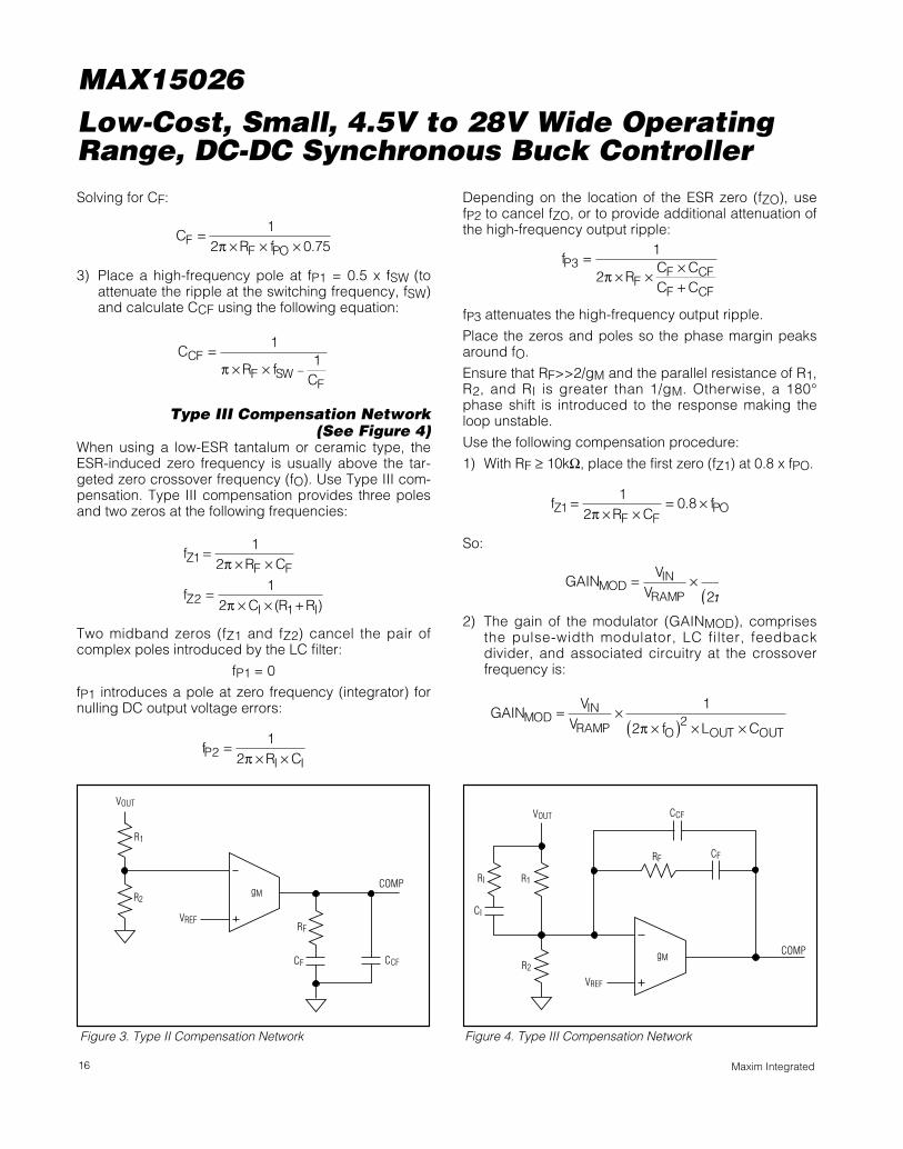
Type III Compensation Network (See Figure 4)
When using a low-ESR tantalum or ceramic type, theESR-induced zero frequency is usually above the tar-geted zero crossover frequency (fO). Use Type III com-pensation. Type III compensation provides three polesand two zeros at the following frequencies:
Two midband zeros (fZ1 and fZ2) cancel the pair ofcomplex poles introduced by the LC filter:
fP1 = 0
fP1 introduces a pole at zero frequency (integrator) fornulling DC output voltage errors:
Depending on the location of the ESR zero (fZO), usefP2 to cancel fZO, or to provide additional attenuation ofthe high-frequency output ripple:
fP3 attenuates the high-frequency output ripple.
Place the zeros and poles so the phase margin peaksaround fO.
Ensure that RF>>2/gM and the parallel resistance of R1,R2, and RI is greater than 1/gM. Otherwise, a 180°phase shift is introduced to the response making theloop unstable.
Use the following compensation procedure:
1) With RF ≥ 10kΩ, place the first zero (fZ1) at 0.8 x fPO.
So:
2) The gain of the modulator (GAINMOD), comprisesthe pulse-width modulator, LC filter, feedbackdivider, and associated circuitry at the crossoverfrequency is:
G NV
V f L C
IN
RAMP O OUT OUT
AI MOD = ××( ) × ×
1
2 2π
G NV
VIN
RAMPAI MOD = ×
(2π
fR C
fZF F
PO11
20 8=
× ×= ×
π.
fR
C CC C
PF
F CF
F CF
31
2=
× ××+
π
fR CP
I I2
12
=× ×π
fR C
fC R R
ZF F
ZI I
1
21
12
12
=× ×
=× × +
π
π ( )
CR f
C
CFF SW
F
=× × −
11π
CR fF
F PO=
× × ×1
2 0 75π .
VREF
R1
VOUT
R2gM
RF
COMP
CF CCF
Figure 3. Type II Compensation Network
VREF
gM
R1
R2
VOUT
RI
COMP
CI
CCF
RF CF
Figure 4. Type III Compensation Network

MAX15026Low-Cost, Small, 4.5V to 28V Wide Operating
Range, DC-DC Synchronous Buck Controller
17Maxim Integrated
The gain of the error amplifier (GAINEA) in midband fre-quencies is:
GAINEA = 2π x fO x C1 x RF
The total loop gain as the product of the modulator gainand the error amplifier gain at fO is 1.
So:
Solving for CI:
3) Use the second pole (fP2) to cancel fZO when fPO <fO < fZO < fSW/2. The frequency response of theloop gain does not flatten out soon after the 0dBcrossover, and maintains a -20dB/decade slope upto 1/2 of the switching frequency. This is likely tooccur if the output capacitor is a low-ESR tantalum.Set fP2 = fZO.
When using a ceramic capacitor, the capacitor ESRzero fZO is likely to be located even above 1/2 theswitching frequency, fPO < fO < fSW/2 < fZO. In thiscase, place the frequency of the second pole (fP2) highenough to not significantly erode the phase margin atthe crossover frequency. For example, set fP2 at 5 x fOso that the contribution to phase loss at the crossoverfrequency fO is only about 11°:
fP2 = 5 x fPO
Once fP2 is known, calculate RI:
4) Place the second zero (fZ2) at 0.2 x fO or at fPO,whichever is lower, and calculate R1 using the fol-lowing equation:
5) Place the third pole (fP3) at 1/2 the switching fre-quency and calculate CCF:
6) Calculate R2 as:
MOSFET SelectionThe MAX15026 step-down controller drives two externallogic-level n-channel MOSFETs. The key selectionparameters to choose these MOSFETs include:
• On-Resistance (RDS(ON))
• Maximum Drain-to-Source Voltage (VDS(MAX))
• Minimum Threshold Voltage (VTH(MIN))
• Total Gate Charge (QG)
• Reverse Transfer Capacitance (CRSS)
• Power Dissipation
The two n-channel MOSFETs must be a logic-level typewith guaranteed on-resistance specifications at VGS =4.5V. For maximum efficiency, choose a high-sideMOSFET that has conduction losses equal to theswitching losses at the typical input voltage. Ensurethat the conduction losses at minimum input voltage donot exceed the MOSFET package thermal limits, or vio-late the overall thermal budget. Also, ensure that theconduction losses plus switching losses at the maxi-mum input voltage do not exceed package ratings orviolate the overall thermal budget. Ensure that the DLgate driver can drive the low-side MOSFET. In particu-lar, check that the dv/dt caused by the high-sideMOSFET turning on does not pull up the low-sideMOSFET gate through the drain-to-gate capacitanceof the low-side MOSFET, which is the most frequentcause of cross-conduction problems.
Check power dissipation when using the internal linearregulator to power the gate drivers. Select MOSFETswith low gate charge so that VCC can power both dri-vers without overheating the device.
PDRIVE = VCC x QG_TOTAL x fSW
where QG_TOTAL is the sum of the gate charges of thetwo external MOSFETs.
RV
V VRFB
OUT FB2 1= ×
−
CC
f R CCFF
SW F F=
× × × ×( ) −2 0 5 1π .
Rf C
RZ I
I12
12
=× ×
−π
Rf CIP I
=× ×
12 2π
CV f L C
V RIRAMP O OUT OUT
IN F=
× × × ×( )×
2π
VV f C L
IN
RAMP O OUT OUT×
× × ×1
2 2( )π
GAIN GAINMOD EA× = 1

MAX15026Low-Cost, Small, 4.5V to 28V Wide OperatingRange, DC-DC Synchronous Buck Controller
18 Maxim Integrated
MA
X1
50
26 Boost Capacitor
The MAX15026 uses a bootstrap circuit to generate thenecessary gate-to-source voltage to turn on the high-side MOSFET. The selected n-channel high-side MOSFET determines the appropriate boost capaci-tance value (CBST in the Typical Application Circuits)according to the following equation:
where QG is the total gate charge of the high-sideMOSFET and ∆VBST is the voltage variation allowed onthe high-side MOSFET driver after turn-on. Choose∆VBST so the available gate-drive voltage is not signifi-cantly degraded (e.g. ∆VBST = 100mV to 300mV) whendetermining CBST. Use a low-ESR ceramic capacitor asthe boost flying capacitor with a minimum value of100nF.
Power DissipationThe maximum power dissipation of the device dependson the thermal resistance from the die to the ambientenvironment and the ambient temperature. The thermalresistance depends on the device package, PCB cop-per area, other thermal mass, and airflow.
The power dissipated into the package (PT) dependson the supply configuration (see the Typical ApplicationCircuits). Use the following equation to calculate powerdissipation:
PT = (VIN - VCC) x ILDO + VDRV x IDRV + VCC x IINwhere ILDO is the current supplied by the internal regu-lator, IDRV is the supply current consumed by the dri-vers at DRV, and IIN is the supply current of theMAX15026 without the contribution of the IDRV, as givenin the Typical Operating Characteristics. For example, inthe application circuit of Figure 5, ILDO = IDRV + IIN andVDRV = VCC so that PT = VIN x (IDRV + IIN).
Use the following equation to estimate the temperaturerise of the die:
TJ = TA + (PT x θJA)
where θJA is the junction-to-ambient thermal imped-ance of the package, PT is power dissipated in thedevice, and TA is the ambient temperature. The θJA is24.4°C/W for 14-pin TDFN package on multilayerboards, with the conditions specified by the respectiveJEDEC standards (JESD51-5, JESD51-7). An accurate
estimation of the junction temperature requires a directmeasurement of the case temperature (TC) when actualoperating conditions significantly deviate from thosedescribed in the JEDEC standards. The junction tem-perature is then:
TJ = TC + (PT x θJC)
Use 8.7°C/W as θJC thermal impedance for the 14-pinTDFN package. The case-to-ambient thermal imped-ance (θCA) is dependent on how well the heat is trans-ferred from the PCB to the ambient. Solder the exposedpad of the TDFN package to a large copper area tospread heat through the board surface, minimizing thecase-to-ambient thermal impedance. Use large copperareas to keep the PCB temperature low.
PCB Layout GuidelinesPlace all power components on the top side of theboard, and run the power stage currents using tracesor copper fills on the top side only. Make a star connec-tion on the top side of traces to GND to minimize volt-age drops in signal paths.
Keep the power traces and load connections short,especially at the ground terminals. This practice isessential for high efficiency and jitter-free operation. Usethick copper PCBs (2oz or above) to enhance efficiency.
Place the MAX15026 adjacent to the synchronous recti-fier MOSFET, preferably on the back side, to keep LX,GND, DH, and DL traces short and wide. Use multiplesmall vias to route these signals from the top to the bot-tom side. Use an internal quiet copper plane to shieldthe analog components on the bottom side from thepower components on the top side.
Make the MAX15026 ground connections as follows:create a small analog ground plane near the device.Connect this plane to GND and use this plane for theground connection for the VIN bypass capacitor, com-pensation components, feedback dividers, VCC capaci-tor, RT resistor, and LIM resistor.
Use Kelvin sense connections for LX and GND to thesynchronous rectifier MOSFET for current limiting toguarantee the current-limit accuracy.
Route high-speed switching nodes (BST, LX, DH, and DL)away from the sensitive analog areas (RT, COMP, LIM,and FB). Group all GND-referred and feedback compo-nents close to the device. Keep the FB and compensationnetwork as small as possible to prevent noise pickup.
CQVBST
G
BST=
∆

MAX15026Low-Cost, Small, 4.5V to 28V Wide Operating
Range, DC-DC Synchronous Buck Controller
19Maxim Integrated
MA
X1
50
26
Typical Application Circuits
R510kΩ
R34.02kΩ
R111.8kΩ
DH
LX
Q2
L11.4µH
BST
DL
ENABLE
PGOOD
VIN
DRV
GND
RT
IN
VCC
PGOOD
LIM
EN
COMP
FB
R74.02kΩ
R615.4kΩ
R427kΩ
R1*
*R1 IS A SMALL-VALUE RESISTOR TO DECOUPLE SWITCHING TRANSIENTS CAUSED BY THE MOSFET DRIVER (2.2Ω).
C62.2µF
C1330µF
PANASONICEEEFCIE331P
4.5V TO 28V
C104.7µF
C768pF
C90.022µF
C868pF
C111500pF
C4470µF
SANYO4C54701
C522µF
C30.47µF
Q1 ( )
VOUT
COILCRAFT MSS1278-142ML
MAX15026
ON-SEMICONDUCTOR NTMFS4835NTIG
( )
ON-SEMICONDUCTOR NTMFS4835NTIG
Single 4.5V to 28V Supply OperationFigure 5 shows an application circuit for a single 4.5V to 28V power-supply operation.
Figure 5. VIN = 4.5V to 28V

MAX15026Low-Cost, Small, 4.5V to 28V Wide OperatingRange, DC-DC Synchronous Buck Controller
20 Maxim Integrated
Typical Application Circuits (continued)
Single 4.5V to 5.5V Supply OperationFigure 6 shows an application circuit for a single 4.5V to 5.5V power-supply operation.
Figure 6. VCC = VIN = VDRV = 4.5V to 5.5V
R1
R3
RLIM
DH
LXL1
BST
DL
ENABLE
PGOOD
VIN
DRV
GND
RT
IN
VCC
PGOOD
LIM
EN
COMP
FB
R2
RT
C1
4.5V TO 5.5V
C4
C3
C2
Q2CF1
CBST
Q1
VOUT
MAX15026

MAX15026Low-Cost, Small, 4.5V to 28V Wide Operating
Range, DC-DC Synchronous Buck Controller
21Maxim Integrated
Typical Application Circuits (continued)
R1
R3
RLIM
DH
LXL1
BST
DL
ENABLE
VAUX
4.5V TO 5.5V
PGOOD
VIN+12V
DRV
GND
RT
IN
VCC
PGOOD
LIM
EN
COMP
FB
R2
RT
C1
C4
C3
C2
Q2CF1
CBST
Q1
VOUT
MAX15026
Auxiliary 5V Supply OperationFigure 7 shows an application circuit for a +12V supply to drive the external MOSFETs and an auxiliary +5V supplyto power the device.
Figure 7. Operation with Auxiliary 5V Supply

MAX15026Low-Cost, Small, 4.5V to 28V Wide OperatingRange, DC-DC Synchronous Buck Controller
22 Maxim Integrated
Chip InformationPROCESS: BiCMOS
PACKAGETYPE
PACKAGECODE
OUTLINE NO.LAND
PATTERN NO.
14 TDFN-EP T1433+2 21-0137 90-0063
Package InformationFor the latest package outline information and land patterns (foot-prints), go to www.maximintegrated.com/packages. Note that a“+”, “#”, or “-” in the package code indicates RoHS status only.Package drawings may show a different suffix character, but thedrawing pertains to the package regardless of RoHS status.

Maxim Integrated cannot assume responsibility for use of any circuitry other than circuitry entirely embodied in a Maxim Integrated product. No circuit patentlicenses are implied. Maxim Integrated reserves the right to change the circuitry and specifications without notice at any time. The parametric values (min andmax limits) shown in the Electrical Characteristics table are guaranteed. Other parametric values quoted in this data sheet are provided for guidance.
Maxim Integrated 160 Rio Robles, San Jose, CA 95134 USA 1-408-601-1000 ________________________________ 23
© 2012 Maxim Integrated Products, Inc. Maxim Integrated and the Maxim Integrated logo are trademarks of Maxim Integrated Products, Inc.
MAX15026Low-Cost, Small, 4.5V to 28V Wide Operating
Range, DC-DC Synchronous Buck ControllerRevision History
REVISIONNUMBER
REVISIONDATE DESCRIPTION PAGES
CHANGED
0 5/08 Initial release —
1 5/09Revised General Description, Ordering Information, Absolute MaximumRatings, Electrical Characteristics, Power-Good Output (PGOOD) section,and Typical Application Circuits
1–4, 10, 15, 19
2 9/10Added MAX15026C; revised General Description, Ordering Information,Electrical Characteristics, Typical Operating Characteristics, and Startupinto a Prebiased Output sections
1–6, 10
3 4/11 Added automotive part to Ordering Information, Absolute Maximum Ratings,and Electrical Characteristics 1, 2, 3
4 2/12 Design modified to meet customer requirements and new OPN added toOrdering Information 1–6, 10, 11
5 11/12 Changed recommended part number for new designs to MAX15026D 1