max30001 - ultra-low-power, single-channel integrated ... · pdf filebioimpedance channel...
TRANSCRIPT

19-100133; Rev 1, 9/17
General DescriptionThe MAX30001 is a complete, biopotential and bioimpedance (BioZ), analog front-end (AFE) solution for wearable applications. It offers high performance for clinical and fitness applications, with ultra-low power for long battery life. The MAX30001 is a single biopotential channel providing electrocardiogram (ECG) waveforms, heart rate and pacemaker edge detection, and a single bioimpedance channel capable of measuring respiration.The biopotential and bioimpedance channels have ESD protection, EMI filtering, internal lead biasing, DC leads-off detection, ultra-low-power, leads-on detection during standby mode, and extensive calibration voltages for built-in self-test. Soft power-up sequencing ensures no large transients are injected into the electrodes. Both channels also have high input impedance, low noise, high CMRR, programmable gain, various low-pass and high-pass filter options, and a high resolution analog-to-digital converter. The biopotential channel is DC coupled, can handle large electrode voltage offsets, and has a fast recovery mode to quickly recover from overdrive conditions, such as defibrillation and electro-surgery. The bioimpedance channel includes integrated programmable current drive, works with common electrodes, and has the flexibility for 2 or 4 electrode measurements. It also has AC lead off detection.The MAX30001 is available in a 28-pin TQFN and 30-bump wafer-level package (WLP), operating over the0°C to +70°C commercial temperature range.
Applications Single-Lead Event Monitors for Arrhythmia Detection Single-Lead Wireless Patches for
In-Patient/Out-Patient Monitoring Chest Band Heart Rate Monitors for Fitness
Applications Bio Authentication and ECG-On-Demand Applications Respiration and Hydration Monitors Impedance Based Heart Rate Detection
Benefits and Features Clinical-Grade ECG and BioZ AFE with High
Resolution Data Converter• 15.9 Bits ENOB with 3.1µVPP (typ) Noise for ECG• 17 Bits ENOB with 1.1µVPP Noise for BioZ
Better Dry Starts Due to Much Improved Real World CMRR and High Input Impedance• Fully Differential Input Structure with CMRR > 100dB
Offers Better Common-Mode to Differential Mode Conversion Due to High Input Impedance
High Input Impedance > 1GΩ for Extremely Low Common-to-Differential Mode
Minimum Signal Attenuation at the Input During Dry Start Due to High Electrode Impedance
High DC Offset Range of ±650mV (1.8V, typ) Allows to Be Used with Wide Variety of Electrodes
High AC Dynamic Range of 65mVPP for ECG and 100mVPP for BioZ Will Help Prevent Saturation in the Presence of Motion/Direct Electrode Hits
Longer Battery Life Compared to Competing Solutions• 85µW at 1.1V Supply Voltage for ECG• 158µW at 1.1V Supply Voltage for BioZ
Leads-On Interrupt Feature Allows to Keep µC in Deep Sleep Mode Until Valid Lead Condition is Detected• Lead-On Detect Current: 0.7µA (typ)
Built-In Heart Rate Detection with Interrupt Feature Eliminates the Need to Run HR Algorithm on the µController• Robust R-R Detection in High Motion Environment
at Extremely Low Power Configurable Interrupts Allows the µC Wake-Up Only
on Every Heart Beat Reducing the Overall System Power
High Accuracy Allows for More Physiological Data Extractions
32-Word ECG and 8-Word BioZ FIFOs Allows the MCU to Stay Powered Down for 256ms with Full Data Acquisition
High-Speed SPI Interface Shutdown Current of 0.5µA (typ)Ordering Information appears at end of data sheet.
MAX30001 Ultra-Low-Power, Single-Channel Integrated Biopotential (ECG, R-to-R, and Pace Detection)
and Bioimpedance (BioZ) AFE

CLOCK DIVIDER w/ PHASE ADJUST
ESD, EMI, INPUT MUX,
DC LEAD CHECK
DECIMATION FILTER
20-BITΣ Σ ADC
INPUTAMP
AAFBIP
BIN
DRVP
DRVN
PGA
BIOIMPEDANCE CHANNEL
MAX30001
AVDD
BANDGAP
COMMON-MODE BUFFER
BIASING PLL
SUPPORT CIRCUITRY
fHFC
fCLKREFERENCE
BUFFER
SPI INTERFACE,ECG FIFO,
ANDREGISTERS
DVDD
SEQUENCER
OVDD
DGNDAGND
CSB
SDI
SCLK
SDO
INTB
INT2B
FCLK
VCM VBG VREF CPLL
20-BIT
PUSH/PULL CURRENT SOURCE
f-3dB =600Hz
-40dB/dec
SELECTABLE PHASE
RBIAS
FASTSETTLING
R-TO-R DETECTOR
ESD, EMI, INPUT MUX,
DC LEAD CHECK
DECIMATION FILTER
18-BITΣ Σ ADC
INPUTAMP
ECGP
ECGN
CAPP
CAPN
PGA
BIOPOTENTIAL CHANNEL
18-BIT
14-BIT
AAF
f-3dB =600Hz
-40dB/dec
PGA
RESPIRATION CANCEL,
DERIVATIVE, SAMPLE/HOLD
WINDOW COMPARE &
RESYNC
BUFFERAOUT
MUX
PACE DETECT CHANNEL
PACEP
PACEN
LPFLPF
INPUTAMP
HPF
-20dB/dec
POL.
SW.
Functional Diagram
MAX30001 Ultra-Low-Power, Single-Channel Integrated Biopotential (ECG, R-to-R, and Pace Detection)
and Bioimpedance (BioZ) AFE
www.maximintegrated.com Maxim Integrated 2

AVDD to AGND ....................................................-0.3V to +2.0VDVDD to DGND ....................................................-0.3V to +2.0VAVDD to DVDD ....................................................-0.3V to +0.3VOVDD to DGND ...................................................-0.3V to +3.6VAGND to DGND ...................................................-0.3V to +0.3VCSB, SCLK, SDI, FCLK to DGND .......................-0.3V to +3.6VSDO, INTB, INT2B
to DGND ........ -0.3V to the lower of (3.6V and OVDD + 0.3V)All Other Pins
to AGND ......... -0.3V to the lower of (2.0V and AVDD + 0.3V)Maximum Current into Any Pin.........................................±50mA
Continuous Power Dissipation (TA = +70ºC) 28-Pin TQFN (derate 34.5mW/ºC above +70ºC) ..........................2758.6mW 30-Bump WLP (derate 24.3mW/ºC above +70ºC) ..........................1945.5mW
Operating Temperature Range ...............................0ºC to +70°CJunction Temperature ......................................................+150°CStorage Temperature Range ............................ -65°C to +150°CLead Temperature (Soldering, 10sec) .............................+300°CSoldering Temperature (reflow) .......................................+260°C
TQFN Junction-to-Ambient Thermal Resistance (θJA) ..........29°C/W Junction-to-Case Thermal Resistance (θJC) .................2°C/W
WLP Junction-to-Ambient Thermal Resistance (θJA) ..........44°C/W
(Note 1)
(VDVDD = VAVDD = +1.1V to +2.0V, VOVDD = +1.65V to +3.6V, fFCLK = 32.768kHz, LN_BIOZ = 1, TA = TMIN to TMAX, unless otherwise noted. Typical values are at VDVDD = VAVDD = +1.8V, VOVDD = +2.5V, TA = +25°C.) (Note 2)
PARAMETER SYMBOL CONDITIONS MIN TYP MAX UNITSECG CHANNEL
AC Differential Input RangeVAVDD = +1.1V, THD < 0.3% -15 +15
mVPPVAVDD = +1.8V, THD < 0.3% ±32.5
DC Differential Input RangeVAVDD = +1.1V, shift from nominal gain < 2% -300 +300
mVVAVDD = +1.8V ±650
Common Mode Input Range
VAVDD = +1.1V, from VMID, shift from nominal gain < 2% -150 +150
mVVAVDD = +1.8V, from VMID, shift from nominal gain < 2% ±550
Common Mode Rejection Ratio CMRR0Ω source impedance, f = 64Hz, TA = +25˚C (Note 3) 100 115
dB(Note 4) 77
ECG Channel Input Referred Noise
BW = 0.05 – 150Hz, GCH = 20x0.77 µVRMS4.6 µVPP
BW = 0.05 – 40Hz, GCH = 20x (Note 3)0.46 1.0 µVRMS3.1 6.6 µVPP
Input Leakage Current TA = +25°C -1 ±0.1 +1 nA
Input Impedance (INA)Common-mode, DC 45 GΩ
Differential, DC 1500 MΩ
Note 1: Package thermal resistances were obtained using the method described in JEDEC specification JESD51-7, using a four-layer board. For detailed information on package thermal considerations, refer to www.maximintegrated.com/thermal-tutorial.
Absolute Maximum Ratings
Stresses beyond those listed under “Absolute Maximum Ratings” may cause permanent damage to the device. These are stress ratings only, and functional operation of the device at these or any other conditions beyond those indicated in the operational sections of the specifications is not implied. Exposure to absolute maximum rating conditions for extended periods may affect device reliability.
Package Thermal Characteristics
Electrical Characteristics
MAX30001 Ultra-Low-Power, Single-Channel Integrated Biopotential (ECG, R-to-R, and Pace Detection)
and Bioimpedance (BioZ) AFE
www.maximintegrated.com Maxim Integrated 3

(VDVDD = VAVDD = +1.1V to +2.0V, VOVDD = +1.65V to +3.6V, fFCLK = 32.768kHz, LN_BIOZ = 1, TA = TMIN to TMAX, unless otherwise noted. Typical values are at VDVDD = VAVDD = +1.8V, VOVDD = +2.5V, TA = +25°C.) (Note 2)
PARAMETER SYMBOL CONDITIONS MIN TYP MAX UNITS
ECG Channel Total Harmonic Distortion THD
VAVDD = +1.80V, VIN = 65mVPP, FIN = 64Hz, GCH = 20x, electrode offset = ±300mV 0.025
%VAVDD = +1.1V, VIN = 30mVPP, FIN = 64Hz, GCH = 20x, electrode offset = ±300mV 0.3
ECG Channel Gain Setting GCH Programmable, see register map 20 to 160 V/V
ECG Channel Gain Error (Excluding Reference)
VAVDD = +1.8V, GCH = 20x, ECGP = ECGN = VMID -2.5 +2.5 %
VAVDD = +1.1V, GCH = 20x, ECGP = ECGN = VMID -4.5 +4.5 %
ECG Channel Offset Error (Note 5) ±0.1 % of FSR
ADC Resolution 18 Bits
ADC Sample Rate Programmable, see register map 125 to 512 SPS
CAPP to CAPN Impedance RHPFFHP = 1/(2π x RHPF x CHPF), CHPF = capacitance between CAPP and CAPN 320 450 600 kΩ
Analog High-Pass Filter Slew Current
Fast recovery enabled (1.8V) 160
µAFast recovery enabled (1.1V) 55
Fast recovery disabled 0.09
Fast Settling Recovery Time CHPF = 10µF, Note: varies by sample rate, see Table 3. 500 ms
Digital Low-Pass Filter Linear phase FIR filter.
DLPF[0:1] = 01 40
HzDLPF[0:1] = 10 100
DLPF[0:1] = 11 150
Digital High-Pass Filter Phase-corrected 1st-order IIR filter. DHPF = 1 0.5 Hz
ECG Power Supply Rejection PSRRLead bias disabled, DC 107
dBLead bias disabled, fSW = 64Hz 110
Electrical Characteristics (continued)
MAX30001 Ultra-Low-Power, Single-Channel Integrated Biopotential (ECG, R-to-R, and Pace Detection)
and Bioimpedance (BioZ) AFE
www.maximintegrated.com Maxim Integrated 4

(VDVDD = VAVDD = +1.1V to +2.0V, VOVDD = +1.65V to +3.6V, fFCLK = 32.768kHz, LN_BIOZ = 1, TA = TMIN to TMAX, unless otherwise noted. Typical values are at VDVDD = VAVDD = +1.8V, VOVDD = +2.5V, TA = +25°C.) (Note 2)
PARAMETER SYMBOL CONDITIONS MIN TYP MAX UNITSECG INPUT MUX
DC Lead Off Check Pullup/pulldown
IMAG[2:0] = 001 5
nA
IMAG[2:0] = 010 10
IMAG[2:0] = 011 20
IMAG[2:0] = 100 50
IMAG[2:0] = 101 100
DC Lead Off Comparator Low Threshold
VTH[1:0] = 11 (Note 6) VMID – 0.50
VVTH[1:0] = 10 (Note 7) VMID –
0.45
VTH[1:0] = 01 (Note 8) VMID – 0.40
VTH[1:0] = 00 VMID – 0.30
DC Lead Off Comparator High Threshold
VTH[1:0] = 11 (Note 6) VMID + 0.50
VVTH[1:0] = 10 (Note 7) VMID +
0.45
VTH[1:0] = 01 (Note 8) VMID + 0.40
VTH[1:0] = 00 VMID + 0.30
Lead Bias Impedance Lead bias enabled
RBIASV[1:0] = 00 50
MΩRBIASV[1:0] = 01 100
RBIASV[1:0] = 10 200
Lead Bias Voltage VMID Lead bias enabled VAVDD/ 2.15 V
Calibration Voltage Magnitude Single-endedVMAG = 0 0.25
mVVMAG = 1 0.50
Calibration Voltage Magnitude Error Single-ended (Note 9) -3 +3 %
Calibration Voltage Frequency Programmable, see Register Map 0.0156 to 256 Hz
Calibration Voltage Pulse Time Programmable, see register map
FIFTY = 0 0.03052 to 62.474 ms
FIFTY = 1 50 %
Electrical Characteristics (continued)
MAX30001 Ultra-Low-Power, Single-Channel Integrated Biopotential (ECG, R-to-R, and Pace Detection)
and Bioimpedance (BioZ) AFE
www.maximintegrated.com Maxim Integrated 5
(VDVDD = VAVDD = +1.1V to +2.0V, VOVDD = +1.65V to +3.6V, fFCLK = 32.768kHz, LN_BIOZ = 1, TA = TMIN to TMAX, unless otherwise noted. Typical values are at VDVDD = VAVDD = +1.8V, VOVDD = +2.5V, TA = +25°C.) (Note 2)
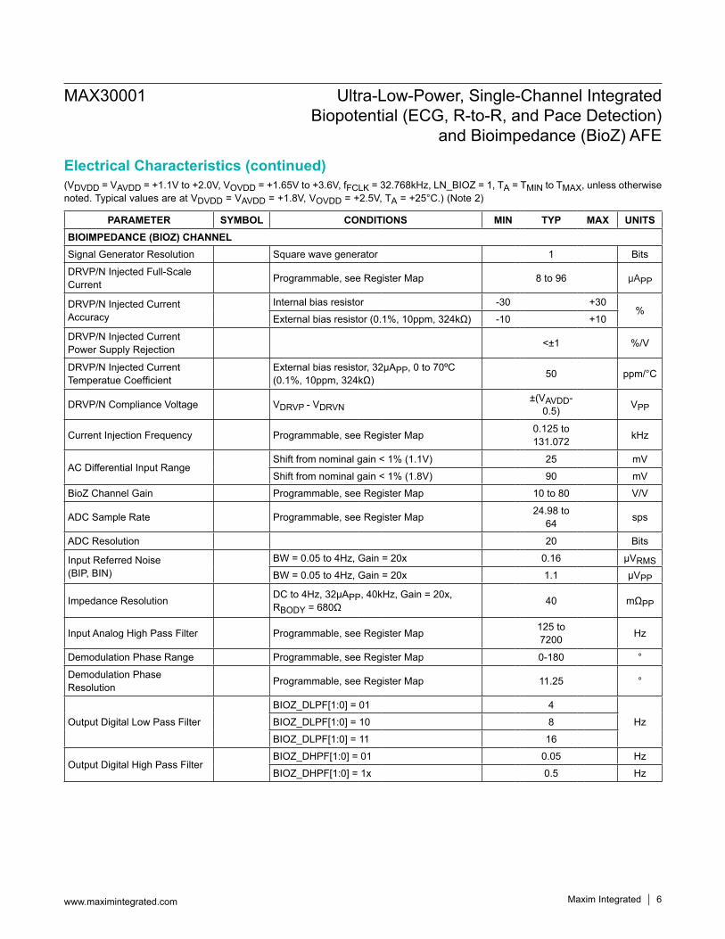
PARAMETER SYMBOL CONDITIONS MIN TYP MAX UNITSBIOIMPEDANCE (BIOZ) CHANNELSignal Generator Resolution Square wave generator 1 Bits
DRVP/N Injected Full-Scale Current Programmable, see Register Map 8 to 96 μAPP
DRVP/N Injected Current Accuracy
Internal bias resistor -30 +30%
External bias resistor (0.1%, 10ppm, 324kΩ) -10 +10
DRVP/N Injected Current Power Supply Rejection <±1 %/V
DRVP/N Injected Current Temperatue Coefficient
External bias resistor, 32μAPP, 0 to 70ºC (0.1%, 10ppm, 324kΩ) 50 ppm/°C
DRVP/N Compliance Voltage VDRVP - VDRVN±(VAVDD-
0.5) VPP
Current Injection Frequency Programmable, see Register Map 0.125 to 131.072 kHz
AC Differential Input RangeShift from nominal gain < 1% (1.1V) 25 mV
Shift from nominal gain < 1% (1.8V) 90 mV
BioZ Channel Gain Programmable, see Register Map 10 to 80 V/V
ADC Sample Rate Programmable, see Register Map 24.98 to 64 sps
ADC Resolution 20 Bits
Input Referred Noise (BIP, BIN)
BW = 0.05 to 4Hz, Gain = 20x 0.16 μVRMSBW = 0.05 to 4Hz, Gain = 20x 1.1 μVPP
Impedance Resolution DC to 4Hz, 32µAPP, 40kHz, Gain = 20x, RBODY = 680Ω 40 mΩPP
Input Analog High Pass Filter Programmable, see Register Map 125 to 7200 Hz
Demodulation Phase Range Programmable, see Register Map 0-180 °
Demodulation Phase Resolution Programmable, see Register Map 11.25 °
Output Digital Low Pass Filter
BIOZ_DLPF[1:0] = 01 4
HzBIOZ_DLPF[1:0] = 10 8
BIOZ_DLPF[1:0] = 11 16
Output Digital High Pass FilterBIOZ_DHPF[1:0] = 01 0.05 Hz
BIOZ_DHPF[1:0] = 1x 0.5 Hz
Electrical Characteristics (continued)
MAX30001 Ultra-Low-Power, Single-Channel Integrated Biopotential (ECG, R-to-R, and Pace Detection)
and Bioimpedance (BioZ) AFE
www.maximintegrated.com Maxim Integrated 6

(VDVDD = VAVDD = +1.1V to +2.0V, VOVDD = +1.65V to +3.6V, fFCLK = 32.768kHz, LN_BIOZ = 1, TA = TMIN to TMAX, unless otherwise noted. Typical values are at VDVDD = VAVDD = +1.8V, VOVDD = +2.5V, TA = +25°C.) (Note 2)
PARAMETER SYMBOL CONDITIONS MIN TYP MAX UNITSBIOIMPEDANCE (BIOZ) INPUT MUX
DC Lead Off Check
IMAG[2:0] = 001 5
nA
IMAG[2:0] = 010 10
IMAG[2:0] = 011 20
IMAG[2:0] = 100 50
IMAG[2:0] = 101 100
DC Lead Off Comparator Low Threshold
DCLOFF_VTH[1:0] = 11 (Note 6) VMID – 0.50
VDCLOFF_VTH[1:0] = 10 (Note 7) VMID –
0.45
DCLOFF_VTH[1:0] = 01 (Note 8) VMID – 0.40
DCLOFF_VTH[1:0] = 00 VMID – 0.30
DC Lead Off Comparator High Threshold
DCLOFF_VTH[1:0] = 11 (Note 6) VMID + 0.50
VDCLOFF_VTH[1:0] = 10 (Note 7) VMID + 0.45
DCLOFF_VTH[1:0] = 01 (Note 8) VMID + 0.40
DCLOFF_VTH[1:0] = 00 VMID + 0.30
Lead Bias Impedance
Lead bias enabled, RBIASV[1:0] = 00 50
MΩLead bias enabled, RBIASV[1:0] = 01 100
Lead bias enabled, RBIASV[1:0] = 10 200
Lead Bias Voltage Lead bias enabled. Programmable, see Register Map
VAVDD/ 2.15 V
Calibration Voltage MagnitudeSingle-ended. VMAG = 0 0.25
mVSingle-ended. VMAG = 1 0.50
Calibration Voltage Error Single-ended. (Note 9) -3 +3 %
Calibration Voltage Frequency Programmable, see Register Map 0.0156 to 256 Hz
Calibration Voltage Pulse Time Programmable, see Register Map
CAL_FIFTY = 0 0.03052 to 62.474 ms
CAL_FIFTY = 1 50 %
Resistive Load Nominal Value RVAL Programmable, see Register Map 0.625 to 5.0 kΩ
Resistive Load Modulation Value RMOD Programmable, see Register Map 15 to 2960 mΩ
Resistive Load Modulation Frequency FMOD Programmable, see Register Map 0.625 to 4.0 Hz
Electrical Characteristics (continued)
MAX30001 Ultra-Low-Power, Single-Channel Integrated Biopotential (ECG, R-to-R, and Pace Detection)
and Bioimpedance (BioZ) AFE
www.maximintegrated.com Maxim Integrated 7

(VDVDD = VAVDD = +1.1V to +2.0V, VOVDD = +1.65V to +3.6V, fFCLK = 32.768kHz, LN_BIOZ = 1, TA = TMIN to TMAX, unless otherwise noted. Typical values are at VDVDD = VAVDD = +1.8V, VOVDD = +2.5V, TA = +25°C.) (Note 2)
PARAMETER SYMBOL CONDITIONS MIN TYP MAX UNITSPACE DETECTIONPace Artifact Width Programmable, see Register Map 0.05 to 2.0 ms
Minimum Pace Artifact Amplitude 0.5 mV
Time Resolution 16 µs
Recovery Time Large Pacer Pulse (100mV to 700mV) 500 µs
AOUT Output Voltage Swing f = 1kHz, THD < 0.2% 100 mVPPINTERNAL REFERENCE/COMMON-MODEVBG Output Voltage VBG 0.650 V
VBG Output Impedance 100 kΩExternal VBG Compensation Capacitor CVBG 1 µF
VREF Output Voltage VREF TA = +25ºC 0.995 1.000 1.005 V
VREF Temperature Coefficient TCREF TA = 0ºC to +70ºC 10 ppm/ºC
VREF Buffer Line Regulation 330 µV/V
VREF Buffer Load Regulation ILOAD = 0 to 100µA 25 µV/µA
External VREF Compensation Capacitor CREF 1 10 µF
VCM Output Voltage VCM 0.650 V
External VCM Compensation Capacitor CCM 1 10 µF
DIGITAL INPUTS (SDI, SCLK, CSB, FCLK)Input-Voltage High VIH 0.7 x VOVDD V
Input-Voltage Low VIL 0.3 x VOVDD V
Input Hysteresis VHYS 0.05 x VOVDD V
Input Capacitance CIN 10 pF
Input Current IIN -1 +1 µA
DIGITAL OUTPUTS (SDO, INTB, INT2B)Output Voltage High VOH ISOURCE = 1mA VOVDD - 0.4 V
Output Voltage Low VOL ISINK = 1mA 0.4 V
Three-State Leakage Current -1 +1 µA
Three-State Output Capacitance 15 pF
POWER SUPPLYAnalog Supply Voltage VAVDD Connect AVDD to DVDD 1.1 2.0 V
Digital Supply Voltage VDVDD Connect DVDD to AVDD 1.1 2.0 V
Interface Supply Voltage VOVDD Power for I/O drivers only 1.65 3.6 V
Electrical Characteristics (continued)
MAX30001 Ultra-Low-Power, Single-Channel Integrated Biopotential (ECG, R-to-R, and Pace Detection)
and Bioimpedance (BioZ) AFE
www.maximintegrated.com Maxim Integrated 8

(VDVDD = VAVDD = +1.1V to +2.0V, VOVDD = +1.65V to +3.6V, fFCLK = 32.768kHz, LN_BIOZ = 1, TA = TMIN to TMAX, unless otherwise noted. Typical values are at VDVDD = VAVDD = +1.8V, VOVDD = +2.5V, TA = +25°C.) (Note 2)
PARAMETER SYMBOL CONDITIONS MIN TYP MAX UNITS
Supply Current IAVDD + IDVDD
ECG channel
VAVDD = VDVDD = +1.1V 76
µA
VAVDD = VDVDD = +1.8V 95
VAVDD = VDVDD = +2.0V 102 120
ECG channel with Pace (Note 3)
VAVDD = VDVDD = +1.1V 100
VAVDD = VDVDD = +1.8V 124
VAVDD = VDVDD = +2.0V 133 150
ECG channel with Pace and AOUT (Note 3)
VAVDD = VDVDD = +1.1V 114
VAVDD = VDVDD = +1.8V 138
VAVDD = VDVDD = +2.0V 147 190
ECG channel with Pace, and BioZ, LN_BIOZ = 0
VAVDD = VDVDD = +1.1V 205
VAVDD = VDVDD = +1.8V 232
VAVDD = VDVDD = +2.0V 242 270
ECG channel with Pace, and BioZ, LN_BIOZ = 1
VAVDD = VDVDD = +1.1V 220
VAVDD = VDVDD = +1.8V 247
VAVDD = VDVDD = +2.0V 256 285
BioZ channel , LN_BIOZ = 0(Note 3)
VAVDD = VDVDD = +1.1V 144
VAVDD = VDVDD = +1.8V 163
VAVDD = VDVDD = +2.0V 170 190
BioZ channel , LN_BIOZ = 1(Note 3)
VAVDD = VDVDD = +1.1V 158
VAVDD = VDVDD = +1.8V 178
VAVDD = VDVDD = +2.0V 185 205
ECG channel and BioZ, LN_BIOZ = 0(Note 3)
VAVDD = VDVDD = +1.1V 186
VAVDD = VDVDD = +1.8V 211
VAVDD = VDVDD = +2.0V 220 250
ECG channel and BioZ, LN_BIOZ = 1(Note 3)
VAVDD = VDVDD = +1.1V 200
VAVDD = VDVDD = +1.8V 225
VAVDD = VDVDD = +2.0V 235 265
ULP Lead On Detect
TA = +70ºC 1.3
TA = +25ºC 0.63 2.5
Interface Supply Current IOVDD
VOVDD = +1.65V, ECG channel at 512sps (Note 10) 0.2
µAVOVDD = 3.6V, ECG channel at 512sps (Note 10) 0.6 1.6
Shutdown CurrentISAVDD + ISDVDD
VAVDD = VDVDD = 2.0V (Note 5)
TA = +70ºC 1.3
µATA = +25ºC 0.58 2.5
ISOVDD VOVDD = 3.6V, VAVDD = VDVDD = 2.0V 1.1
ESD PROTECTION
ECGP, ECGN, BIP, BINIEC 61000-4-2 Contact Discharge (Note 11) ±8
kVIEC 61000-4-2 Air-Gap Discharge (Note 11) ±15
Electrical Characteristics (continued)
MAX30001 Ultra-Low-Power, Single-Channel Integrated Biopotential (ECG, R-to-R, and Pace Detection)
and Bioimpedance (BioZ) AFE
www.maximintegrated.com Maxim Integrated 9

(VDVDD = VAVDD = +1.1V to +2.0V, VOVDD = +1.65V to +3.6V, fFCLK = 32.768kHz, LN_BIOZ = 1, TA = TMIN to TMAX, unless otherwise noted. Typical values are at VDVDD = VAVDD = +1.8V, VOVDD = +2.5V, TA = +25°C.) (Note 2)
Note 2: All devices are 100% production tested at TA = +25ºC. Specifications over the operating temperature range and relevant supply voltage range are guaranteed by design and characterization.
Note 3: Guaranteed by design and characterization. Not tested in production.Note 4: One electrode drive with <10Ω source impedance, the other driven with 51kΩ in parallel with a 47nF per IEC60601-2-47.Note 5: Inputs connected to 51kΩ in parallel with a 47nF to VCM.Note 6: Use this setting only for VAVDD = VDVDD ≥ 1.65V.Note 7: Use this setting only for VAVDD = VDVDD ≥ 1.55V.Note 8: Use this setting only for VAVDD = VDVDD ≥ 1.45V.Note 9: This specification defines the accuracy of the calibration voltage source as applied to the ECG input, not as measured
through the ADC channel.Note 10: fSCLK = 4MHz, burst mode, EFIT = 8, CSDO = CINTB = 50pF.Note 11: ESD test performed with 1kΩ series resistor designed to withstand 8kV surge voltage.
PARAMETER SYMBOL CONDITIONS MIN TYP MAX UNITSTIMING CHARACTERISTICS (NOTE 3)SCLK Frequency fSCLK 0 12 MHz
SCLK Period tCP 83 ns
SCLK Pulse Width High tCH 15 ns
SCLK Pulse Width Low tCL 15 ns
CSB Fall to SCLK Rise Setup Time tCSS0 To 1st SCLK rising edge (RE) 15 ns
CSB Fall to SCLK Rise Hold Time tCSH0 Applies to inactive RE preceding 1st RE 0 ns
CSB Rise to SCLK Rise Hold Time tCSH1 Applies to 32nd RE, executed write 10 ns
CSB Rise to SCLK Rise tCSA Applies to 32nd RE, aborted write sequence 15 ns
SCLK Rise to CSB Fall tCSF Applies to 32nd RE 100 ns
CSB Pulse-Width High tCSPW 20 ns
SDI-to-SCLK Rise Setup Time tDS 8 ns
SDI to SCLK Rise Hold Time tDH 8 ns
SCLK Fall to SDO Transition tDOT
CLOAD = 20pF 40 ns
CLOAD = 20pF, VAVDD = VDVDD ≥ 1.8V, VDVDD ≥ 2.5V 20 ns
SCLK Fall to SDO Hold tDOH CLOAD = 20pF 2 ns
CSB Fall to SDO Fall tDOE Enable time, CLOAD = 20pF 30 ns
CSB Rise to SDO Hi-Z tDOZ Disable time 35 ns
FCLK Frequency fFCLK External reference clock 32.768 kHz
FCLK Period tFP 30.52 µs
FCLK Pulse-Width High tFH 50% duty cycle assumed 15.26 µs
FCLK Pulse-Width Low tFL 50% duty cycle assumed 15.26 µs
Timing Characteristics (Note 3)
MAX30001 Ultra-Low-Power, Single-Channel Integrated Biopotential (ECG, R-to-R, and Pace Detection)
and Bioimpedance (BioZ) AFE
www.maximintegrated.com Maxim Integrated 10

Figure 1a. SPI Timing Diagram
Figure 1b. FCLK Timing Diagram
DO23
tCSH1
tCSF
1 2 3 4 5 6 7 8 31
A5A6 A4 A3 A2 A1 A0 R/WB DIN1 DIN0
tDS
tCSS0
SDI
tCSH0
32 1'
tCSA
tCSPW
DO1
tDOE
Z Z
9 10
DIN23 DIN22
DO0
A6'
DO22
SCLK
CSB
SDO
tDHtCP
tCH
tCL
tDOT tDOH
tDOZ
tFP
FCLK
tFH tFL
MAX30001 Ultra-Low-Power, Single-Channel Integrated Biopotential (ECG, R-to-R, and Pace Detection)
and Bioimpedance (BioZ) AFE
www.maximintegrated.com Maxim Integrated 11

(VDVDD = VAVDD = 1.8V, VOVDD = 2.5V, TA = +25°C, unless otherwise noted.)Typical Operating Characteristics
-200
-180
-160
-140
-120
-100
-80
-60
-40
-20
0
0 64 128 192 256
NOIS
E (d
B)
FREQUENCY (Hz)
ECG NOISE SPECTRUM vs. FREQUENCYINPUTS SHORTED, GAIN = 160, LPF = 150Hz
toc04
-250
-200
-150
-100
-50
0
0 8 16 24 32
NOIS
E (d
B)
FREQUENCY (Hz)
BIOZ NOISE SPECTRUM vs. FREQUENCYINPUTS SHORTED, GAIN = 10, LPF = 4Hz
toc05
-250
-200
-150
-100
-50
0
0 8 16 24 32
NOIS
E (d
B)
FREQUENCY (Hz)
BIOZ NOISE SPECTRUM vs. FREQUENCYINPUTS SHORTED, GAIN = 10, LPF = 16Hz
toc06
-200
-180
-160
-140
-120
-100
-80
-60
-40
-20
0
0 64 128 192 256
NOIS
E (d
B)
FREQUENCY (Hz)
ECG NOISE SPECTRUM vs. FREQUENCYINPUTS SHORTED, GAIN = 20, LPF = 40Hz
toc01
-200
-180
-160
-140
-120
-100
-80
-60
-40
-20
0
0 64 128 192 256
NOIS
E (d
B)
FREQUENCY (Hz)
ECG NOISE SPECTRUM vs. FREQUENCYINPUTS SHORTED, GAIN = 20, LPF = 150Hz
toc02
-200
-180
-160
-140
-120
-100
-80
-60
-40
-20
0
0 64 128 192 256
NOIS
E (d
B)
FREQUENCY (Hz)
ECG NOISE SPECTRUM vs. FREQUENCYINPUTS SHORTED, GAIN = 160, LPF = 40Hz
toc03
-250
-200
-150
-100
-50
0
0 8 16 24 32
NOIS
E (d
B)
FREQUENCY (Hz)
BIOZ NOISE SPECTRUM vs. FREQUENCYINPUTS SHORTED, GAIN = 80, LPF = 4Hz
toc07
-250
-200
-150
-100
-50
0
0 8 16 24 32
NOIS
E (d
B)
FREQUENCY (Hz)
BIOZ NOISE SPECTRUM vs. FREQUENCYINPUTS SHORTED, GAIN = 80, LPF = 16Hz
toc08
-4
-3
-2
-1
0
1
2
3
4
0 2 4 6 8 10
NOIS
E (µ
V)
TIME (s)
ECG INPUT-REFERRED NOISE vs. TIMEGAIN = 20, LPF = 40Hz (10s)
toc09
MAX30001 Ultra-Low-Power, Single-Channel Integrated Biopotential (ECG, R-to-R, and Pace Detection)
and Bioimpedance (BioZ) AFE
Maxim Integrated 12www.maximintegrated.com

(VDVDD = VAVDD = 1.8V, VOVDD = 2.5V, TA = +25°C, unless otherwise noted.)Typical Operating Characteristics (continued)
0
200
400
600
800
1000
1200
1400
1600
1800
-50 -49 -48 -47 -46 -45 -44 -43 -42
NUM
BER
OF
OCC
URRE
NCES
ADC CODE
ECG NOISE HISTOGRAMGAIN = 20, LPF = 40Hz
toc13STDEV = 0.47µVOFFSET = -17.71µV
-4
-3
-2
-1
0
1
2
3
4
0 2 4 6 8 10
NOIS
E (µ
V)
TIME (s)
ECG INPUT-REFERRED NOISE vs. TIME GAIN = 20, LPF = 150Hz (10s)
toc10
0
20
40
60
80
100
120
140
160
180
200
-72 -65 -58 -51 -44 -37 -30 -23 -16 -9 -2 5 12 19
NUM
BER
OF
OCC
URRE
NCES
ADC CODE
ECG NOISE HISTOGRAMGAIN = 160, LPF = 150Hz
toc16
-4
-3
-2
-1
0
1
2
3
4
0 2 4 6 8 10
NOIS
E (µ
V)
TIME (s)
ECG INPUT-REFERRED NOISE vs. TIME GAIN = 160, LPF = 40Hz (10s)
toc11
60
70
80
90
100
110
120
130
0 64 128 192 256
CMRR
(dB)
FREQUENCY (Hz)
ECG CMRR vs. FREQUENCY(MISMATCHED LOAD IS 0Ω ON ECGP,
51kΩ || 47nF ON ECGN)
0Ω ON BOTH INPUTS, GAIN = 20
toc17
51kΩ || 47nF LOAD ON BOTH INPUTS,
GAIN = 20
MISMATCHED INPUTS, GAIN = 160 MISMATCHED INPUTS,
GAIN = 20
51kΩ || 47nF LOAD ON BOTH INPUTS,
GAIN = 160
-4
-3
-2
-1
0
1
2
3
4
0 2 4 6 8 10
NOIS
E (µ
V)
TIME (s)
ECG INPUT-REFERRED NOISE vs. TIME GAIN = 160, LPF = 150Hz (10s)
toc12
1
10
100
1000
0 0.5 1 1.5 2 2.5
PSRR
(LSB
/V)
FREQUENCY (MHz)
ECG PSRR vs. FREQUENCY
toc18
0
100
200
300
400
500
600
700
800
900
1000
-54 -52 -50 -48 -46 -44 -42 -40 -38
NUM
BER
OF
OCC
URRE
NCES
ADC CODE
ECG NOISE HISTOGRAMGAIN = 20, LPF = 150Hz
toc14
0
50
100
150
200
250
300
350
400
-45 -41 -37 -33 -29 -25 -21 -17 -13 -9 -5 -1 3
NUM
BER
OF
OCC
URRE
NCES
ADC CODE
ECG NOISE HISTOGRAMGAIN = 160, LPF = 40Hz
toc15
MAX30001 Ultra-Low-Power, Single-Channel Integrated Biopotential (ECG, R-to-R, and Pace Detection)
and Bioimpedance (BioZ) AFE
Maxim Integrated 13www.maximintegrated.com

(VDVDD = VAVDD = 1.8V, VOVDD = 2.5V, TA = +25°C, unless otherwise noted.)Typical Operating Characteristics (continued)
1
10
100
1000
10000
100000
1000000
10000000
-400 -200 0 200 400
INPU
T RE
SIST
ANCE
(MΩ
)
VCM-VMID (mV)
NO LEAD BIAS
ECG COMMON-MODE INPUT RESISTANCE vs. VOLTAGE
toc22
50MΩLEAD BIAS
100MΩLEAD BIAS
200MΩLEAD BIAS
1
10
100
1000
10000
0 10 20 30 40 50 60 70
INPU
T RE
SIST
ANCE
(MΩ
)
TEMPERATURE (°C)
NO LEAD BIAS
ECG DIFFERENTIAL INPUT RESISTANCE vs. TEMPERATURE
toc23
50MΩLEAD BIAS
100MΩLEAD BIAS
200MΩLEAD BIAS
1
10
100
1000
10000
100000
1000000
0 10 20 30 40 50 60 70
INPU
T RE
SIST
ANCE
(MΩ
)
TEMPERATURE (°C)
NO LEAD BIAS
ECG COMMON-MODE INPUT RESISTANCE vs. TEMPERATURE
toc24
50MΩLEAD BIAS
100MΩLEAD BIAS
200MΩLEAD BIAS
1
10
100
1000
10000
0 64 128 192 256
INPU
T RE
SIST
ANCE
(MΩ
)
FREQUENCY (Hz)
NOLEAD BIAS
ECG DIFFERENTIAL INPUT RESISTANCE vs. FREQUENCY
toc19
50MΩLEAD BIAS 100MΩ
LEAD BIAS
200MΩLEAD BIAS
1
10
100
1000
10000
0 64 128 192 256
INPU
T RE
SIST
ANCE
(MΩ
)
FREQUENCY (Hz)
NO LEAD BIAS
ECG COMMON-MODE INPUT RESISTANCE vs. FREQUENCY
toc20
50MΩLEAD BIAS
100MΩLEAD BIAS
200MΩLEAD BIAS
1
10
100
1000
10000
-500 -300 -100 100 300 500
INPU
T RE
SIST
ANCE
(MΩ
)
VECGP-VECGN (mV)
NO LEAD BIAS
ECG DIFFERENTIAL INPUT RESISTANCE vs. VOLTAGE
toc21
50MΩLEAD BIAS
100MΩLEAD BIAS
200MΩLEAD BIAS
10
100
1000
10000
100000
1000000
-800 -600 -400 -200 0 200 400 600 800
INPU
T RE
SIST
ANCE
(MΩ
)
VBIP-VBIN (mV)
NOLEAD BIAS
BIOZ DIFFERENTIAL INPUT RESISTANCE vs. VOLTAGE
toc25
50MΩ LEAD BIAS
100MΩLEAD BIAS
200MΩLEAD BIAS
10
100
1000
10000
100000
1000000
-600 -400 -200 0 200 400 600
INPU
T RE
SIST
ANCE
(MΩ
)
VCM-VMID (mV)
NOLEAD BIAS
BIOZ COMMON-MODE INPUT RESISTANCE vs. VOLTAGE
toc26
50MΩLEAD BIAS
100MΩLEAD BIAS
200MΩLEAD BIAS
-120
-100
-80
-60
-40
-20
0
0 64 128 192 256
THD
(dB)
FREQUENCY (Hz)
ECG THD vs. FREQUENCY
ECG GAIN = 40
toc27
ECG GAIN = 20
ECG GAIN = 80
ECG GAIN = 160
MAX30001 Ultra-Low-Power, Single-Channel Integrated Biopotential (ECG, R-to-R, and Pace Detection)
and Bioimpedance (BioZ) AFE
Maxim Integrated 14www.maximintegrated.com

(VDVDD = VAVDD = 1.8V, VOVDD = 2.5V, TA = +25°C, unless otherwise noted.)Typical Operating Characteristics (continued)
-120
-100
-80
-60
-40
-20
0
20
0.1 1 10 100 1000
GAI
N (d
B)
FREQUENCY (Hz)
ECG FILTER RESPONSEHPF = 0.5Hz, LPF = 100Hz
GAIN = 20V/V, SAMPLE RATE = 512
toc31CHPF = 10µF
DHPF = 0.5HzDLPF = 100Hz
-120
-100
-80
-60
-40
-20
0
0 20 40 60 80 100
THD
(dB)
AMPLITDUE (mVPk-Pk)
ECG THD vs. INPUT AMPLITUDE
ECG GAIN = 40
toc28
ECG GAIN = 20
ECG GAIN = 80
ECG GAIN = 160
0
20
40
60
80
100
120
0 10 20 30 40 50 60 70
SHUT
DOW
N CU
RREN
T (µ
A)
TEMPERATURE (°C)
BIOZ DRIVE CURRENT vs. TEMPERATUREINTERNAL BIASING
96µA
toc34
80µA
64µA
48µA
32µA
16µA
8µA
-200
-180
-160
-140
-120
-100
-80
-60
-40
-20
0
0 64 128 192 256
MAG
NITU
DE (
dB)
FREQUENCY (Hz)
ECG FFTGAIN = 20, FIN = 25Hz, LPF BYPASSED
toc29
0
10
20
30
40
50
60
70
80
90
100
0 10 20 30 40 50 60 70
SHUT
DOW
N CU
RREN
T (µ
A)
TEMPERATURE (°C)
BIOZ DRIVE CURRENT vs. TEMPERATUREEXTERNAL BIASING
toc35
80 µA
8 µA
32 µA
-120
-100
-80
-60
-40
-20
0
20
0.1 1 10 100 1000
GAI
N (d
B)
FREQUENCY (Hz)
ECG FILTER RESPONSEHPF = 0.5Hz, LPF = 40Hz
GAIN = 20V/V, SAMPLE RATE = 512
toc30CHPF = 10µF
0.00
0.20
0.40
0.60
0.80
1.00
1.20
1.40
0 10 20 30 40 50 60 70
SHUT
DOW
N CU
RREN
T (µ
A)
TEMPERATURE (°C)
DVDD SHUTDOWN CURRENT
VDVDD = +2.0V
toc36
VDVDD = +1.8V
VDVDD = +1.1V
-120
-100
-80
-60
-40
-20
0
20
0.1 1 10 100 1000
GAI
N (d
B)
FREQUENCY (Hz)
ECG FILTER RESPONSEHPF = 0.5Hz, LPF = 150Hz
GAIN = 20V/V, SAMPLE RATE = 512
toc32CHPF = 10µF
DHPF = 0.5HzDLPF = 150Hz
999.6
999.7
999.8
999.9
1000
1000.1
1000.2
1000.3
1000.4
1000.5
1000.6
0 10 20 30 40 50 60 70
VREF
(mV)
TEMPERATURE (°C)
VREF vs. TEMPERATURE
toc33
MAX30001 Ultra-Low-Power, Single-Channel Integrated Biopotential (ECG, R-to-R, and Pace Detection)
and Bioimpedance (BioZ) AFE
Maxim Integrated 15www.maximintegrated.com

(VDVDD = VAVDD = 1.8V, VOVDD = 2.5V, TA = +25°C, unless otherwise noted.)Typical Operating Characteristics (continued)
60
70
80
90
100
110
120
130
140
150
0 10 20 30 40 50 60 70
AVDD
AND
DVD
D SU
PPLY
CUR
RENT
(µA
)
TEMPERATURE (°C)
AVDD AND DVDD SUPPLY CURRENTvs. TEMPERATURE
(ECG, PACE ENABLED)
1.1V
toc40
1.8V
2.0V
100
110
120
130
140
150
160
170
180
190
200
0 10 20 30 40 50 60 70
AVDD
AND
DVD
D SU
PPLY
CUR
RENT
(µA
)
TEMPERATURE (°C)
AVDD AND DVDD SUPPLY CURRENTvs. TEMPERATURE
(BIOZ ENABLED, LN_BIOZ = 0)
1.1V
toc41
1.8V
2.0V
IDRV = 32 µA
0.00
0.02
0.04
0.06
0.08
0.10
0.12
0 10 20 30 40 50 60 70
SHUT
DOW
N CU
RREN
T (µ
A)
TEMPERATURE (°C)
AVDD SHUTDOWN CURRENT
VAVDD = +2.0V
toc37
VAVDD = +1.8V
VAVDD = +1.1V
VAVDD = +1.5V
0.00
0.05
0.10
0.15
0.20
0.25
0.30
0 10 20 30 40 50 60 70
SHUT
DOW
N CU
RREN
T (µ
A)TEMPERATURE (°C)
OVDD SHUTDOWN CURRENT
VOVDD = +2.0V
toc38
VOVDD = +1.8V
VOVDD = +1.1V
VOVDD = +1.5V
60
65
70
75
80
85
90
95
100
105
110
0 10 20 30 40 50 60 70
AVDD
AND
DVD
D SU
PPLY
CUR
RENT
(µA
)
TEMPERATURE (°C)
AVDD AND DVDD SUPPLY CURRENTvs. TEMPERATURE
(ECG ENABLED)
1.1V
toc39
1.8V
2.0V
160
170
180
190
200
210
220
230
240
250
260
0 10 20 30 40 50 60 70
AVDD
AND
DVD
D SU
PPLY
CUR
RENT
(µA
)
TEMPERATURE (°C)
1.1V
toc42
1.8V
2.0V
AVDD AND DVDD SUPPLY CURRENTvs. TEMPERATURE
(ECG, PACE, BIOZ ENABLED, LN_BIOZ = 0)
1.1V
1.8V
2.0V
IDRV = 32 µA
MAX30001 Ultra-Low-Power, Single-Channel Integrated Biopotential (ECG, R-to-R, and Pace Detection)
and Bioimpedance (BioZ) AFE
Maxim Integrated 16www.maximintegrated.com

(VDVDD = VAVDD = 1.8V, VOVDD = 2.5V, TA = +25°C, unless otherwise noted.)Typical Operating Characteristics (continued)
0
0.2
0.4
0.6
0.8
1
1.2
0 10 20 30 40 50 60 70
AVDD
AND
DVD
D UL
P CU
RREN
T (µ
A)
TEMPERATURE (°C)
AVDD AND DVDD ULP CURRENTvs. TEMPERATURE
1.1V
toc43
1.5V
2.0V
1.8V1.8V
-1.50
-1.00
-0.50
0.00
0.50
1.00
1.50
2.00
0 0.1 0.2 0.3 0.4 0.5 0.6
VOLT
AGE
(mV)
TIME (s)
ECG PACEMAKER PULSE TOLERANCE2mV, 0.1ms PULSE
ECG SIGNAL
toc472mV, 0.1ms Pulse
-1.5
-1
-0.5
0
0.5
1
1.5
2
2.5
0 0.1 0.2 0.3 0.4 0.5 0.6
VOLT
AGE
(mV)
TIME (s)
ECG PACEMAKER PULSE TOLERANCE2mV, 2.0ms PULSE
ECG SIGNAL
toc442mv, 2.0ms PULSE
-1.5
-1
-0.5
0
0.5
1
1.5
2
2.5
0 0.1 0.2 0.3 0.4 0.5 0.6
VOLT
AGE
(mV)
TIME (s)
ECG PACEMAKER PULSE TOLERANCE200mV, 2.0ms PULSE
ECG SIGNAL
toc45200mV 2.0ms PULSE
-1.50
-1.00
-0.50
0.00
0.50
1.00
1.50
2.00
0 0.1 0.2 0.3 0.4 0.5 0.6
VOLT
AGE
(mV)
TIME (s)
ECG PACEMAKER PULSE TOLERANCE20mV, 0.1ms PULSE
ECG SIGNAL
toc4620mV, 0.1ms PULSE
MAX30001 Ultra-Low-Power, Single-Channel Integrated Biopotential (ECG, R-to-R, and Pace Detection)
and Bioimpedance (BioZ) AFE
Maxim Integrated 17www.maximintegrated.com

BUMP PINNAME FUNCTION
WLP TQFN
A1 1 DRVP Positive Output Current Source for Bio-Impedance Excitation. Requires a series capacitor between pin and electrode.
A2 2 DRVN Negative Output Current Source for Bio-Impedance Excitation. Requires a series capacitor between pin and electrode.
A3 4 BIN Bioimpedance Negative Input.
A4 5 BIP Bioimpedance Positive Input.
A5 6 ECGP ECG Positive Input.
A6 7 ECGN ECG Negative Input.
B1 27 VBG Bandgap Noise Filter Output. Connect a 1.0μF X7R ceramic capacitor between VBG and AGND.
B2 26 RBIAS External Resistor Bias. Connect a low tempco resistor between RBIAS and AGND. If external bias generator is not used then RBIAS can be left floating.
B3, B4, C3, C4, D4 3, 8, 28 AGND Analog Power and Reference Ground. Connect into the printed circuit board ground
plane.
B5 10 CAPNAnalog High-Pass Filter Input. Connect a 1μF X7R capacitor (CHPF) between CAPP and CAPN to form a 0.5Hz high-pass response in the ECG channel. Select a capaitor with a high voltage rating (25V) to improve linearity of the ECG signal path.
MAX30001
TQFN(5mm x 5mm)
*CONNECT EP TO AGND
TOP VIEW
DR
VN BIN
BIP
ECG
P
ECG
N
DR
VP
INT2
B
SDO
SDI
INTB
SCLK
CSB
VCM
RBIAS
VBG
DGND
CPLL
CAPN
CAPP
AGN
DO
VDD
AGND AGND
+
AOUT
DVDDVREF
FCLKAVDD 14
8
9
10
11
12
13
22
28
27
26
25
24
23
15161718192021
7654321
*EP
TEXTOP VIEW(BUMP SIDE DOWN)
A
B
C
D
WLP(2.7mm x 2.9mm)
E
DRVP
1
DRVN
2
BIN
3
BIP ECGP ECGN
VBG RBIAS AGND AGND CAPN CAPP
VCM AOUT AGND AGND DGND CPLL
VREF INTB OVDD AGND FCLK DVDD
AVDD INT2B SDO SDI SCLK CSB
4 5 6
MAX30001
Pin Configurations
Pin Description
MAX30001 Ultra-Low-Power, Single-Channel Integrated Biopotential (ECG, R-to-R, and Pace Detection)
and Bioimpedance (BioZ) AFE
www.maximintegrated.com Maxim Integrated 18

BUMP PINNAME FUNCTION
WLP TQFN
B6 9 CAPPAnalog High-Pass Filter Input. Connect a 1μF X7R capacitor (CHPF) between CAPP and CAPN to form a 0.5Hz high-pass response in the ECG channel. Select a capaitor with a high voltage rating (25V) to improve linearity of the ECG signal path.
C1 25 VCM Common Mode Buffer Output. Connect a 10μF X5R ceramic capacitor between VCM and AGND.
C2 24 AOUT Analog Output Voltage of the Pace Channel. Programmable to select where in the signal path to output to AOUT.
C5 12 Digital Ground for Both Digital Core and I/O Pad Drivers. Recommended to connect to AGND plane.
C6 11 CPLL PLL Loop Filter Input. Connect 1nF capacitor between CPLL and AGND.
D1 23 VREF ADC Reference Buffer Output. Connect a 10μF X5R ceramic capacitor between VREF and AGND.
D2 21 INTB Interrupt Output. INTB is an active low status output. It can be used to interrupt an external device.
D3 19 OVDD Logic Interface Supply Voltage.
D5 14 FCLK External 32.768kHz Clock that Controls the Sampling of the Internal Sigma-Delta Converters and Decimator.
D6 13 DVDD Digital Core Supply voltage. Connect to AVDD.
E1 22 AVDD Analog Core Supply Voltage. Connect to DVDD.
E2 20 INT2B Interrupt 2 Output. INT2B is an active-low status output. It can be used to interrupt an external device.
E3 18 SDO Serial Data Output. SDO will change state on the falling edge of SCLK when CSB is low. SDO is three-stated when CSB is high.
E4 17 SDI Serial Data Input. SDI is sampled into the device on the rising edge of SCLK whenCSB is low.
E5 16 SCLK Serial Clock Input. Clocks data in and out of the serial interface when CSB is low.
E6 15 CSB Active-Low Chip-Select Input. Enables the serial interface.
— Exposed Pad. Connect EP to AGND.
Pin Description (continued)
MAX30001 Ultra-Low-Power, Single-Channel Integrated Biopotential (ECG, R-to-R, and Pace Detection)
and Bioimpedance (BioZ) AFE
www.maximintegrated.com Maxim Integrated 19

Detailed DescriptionECG ChannelFigure 2 illustrates the ECG channel block diagram, excluding the ADC. The channel comprises an input MUX, a fast-recovering instrumentation amplifier, an anti-alias filter, and a programmable gain amplifier. The input MUX includes several features such as ESD protection, EMI filtering, lead biasing, leads off checking, and ultra-low power leads-on checking. The output of this analog channel drives a high-resolution ADC.
Input MUXThe ECG input MUX shown in Figure 3 contains integrated ESD and EMI protection, DC leads off detect current sources, lead-on detect, series isolation switches, lead biasing, and a programmable calibration voltage source to enable channel built in self-test.
EMI Filtering and ESD ProtectionEMI filtering of the ECGP and ECGN inputs consists of a single pole, low pass, differential, and common mode filter with the pole located at approximately 2MHz. The ECGP and ECGN inputs also have input clamps that protect the inputs from ESD events.
±8kV using the Contact Discharge method specified in IEC61000-4-2 ESD
±15kV using the Air Gap Discharge method specified in IEC61000-4-2 ESD
For IEC61000-4-2 ESD protection, use 1kΩ series resistors on ECGP and ECGN that is rated to withstand ±8kV surge voltages.
Figure 2. ECG Channel Input Amplifier and PGA Excluding the ADC
FASTSETTLING
ESD, EMI, INPUT MUX, DC LEAD
CHECK
INPUTAMP
AAF
f-3dB = 600Hz-40dB/dec
ECGP
ECGN
CAPP
CAPN
PGA
MAX30001
PCB
CHPF
MAX30001 Ultra-Low-Power, Single-Channel Integrated Biopotential (ECG, R-to-R, and Pace Detection)
and Bioimpedance (BioZ) AFE
www.maximintegrated.com Maxim Integrated 20

Figure 3. ECG Input MUX
AVDD
AGND
AVDD
AGND
DC LEAD-OFF CHECKESD PROTECTIONAND
EMI FILTER
AVDD
AGND
5MΩ
15MΩ
ULP LEAD-ON CHECK
VMID
VMID
LEADBIAS
50,100,
200MΩ
50,100,
200MΩ
AVDD
AGND
CALIBRATION VOLTAGE
AGND AGND AGND
AGND AGND AGND
5-100nA
5-100nA
5-100nA
ECGP
ECGN
TO ECGINA IN+
TO ECGINA IN-
VTHH
VTHL
VTHH
VTHL
±0.25, ±0.5mV,Uni, Bipolar,1/64 – 256Hz,Time High
±0.25, ±0.5mV,Uni, Bipolar,1/64 – 256Hz,Duty Cycle
5-100nA
AGND
AVDD
3R
R
INPUT AND POLARITY SWITCHES
MAX30001
MAX30001 Ultra-Low-Power, Single-Channel Integrated Biopotential (ECG, R-to-R, and Pace Detection)
and Bioimpedance (BioZ) AFE
www.maximintegrated.com Maxim Integrated 21

DC Leads-Off Detection and ULP Leads-On DetectionThe input MUX leads-off detect circuitry consists of programmable sink/source DC current sources that allow for DC leads-off detection, while the channel is powered up in normal operation and an ultra-low-power (ULP) leads-on detect while the channel is powered-down.The MAX30001 accomplishes DC leads-off detection by applying a DC current to pull the ECG input voltage up to above VMID + VTH or down to below VMID - VTH. The current sources have user selectable values of 0nA, 5nA, 10nA, 20nA, 50nA, and 100nA that allow coverage of dry and wet electrode impedance ranges. Supported thresholds are VMID ± 300mV (recommended), VMID ±400mV, VMID ± 450mV, and VMID ± 500mV. A threshold of 400mV, 450mV, and 500mV must only be used when VAVDD ≥ 1.45V, 1.55V, and 1.65V, respectively. A dynamic comparator protects against false flags generated by the input amplifier and input chopping. The comparator checks for a minimum continuous violation (or threshold exceeded) of 115ms to 140ms depending on the setting of FMSTR[1:0] before asserting any one of the LDOFF_xx interrupt flags (Figure 4). See registers CNFG_GEN (0x10) and CNFG_EMUX (0x14) for configuration settings and see Table 1 for recommended values given electrode type and supply voltage. The ULP lead on detect operates by pulling ECGN low with a pulldown resistance larger than 5MΩ and pulling ECGP high with a pullup resistance larger than 15MΩ. A low-power comparator determines if ECGP is pulled below a predefined threshold that occurs when both electrodes make contact with the body. When the impedance between ECGP and ECGN is less than 20MΩ, an interrupt LONINT is asserted, alerting the µC to a leads-on condition.A 0nA/VMID ± 300mV selection is available allowing monitoring of the input compliance of the INA during non- DC lead-off checks.
Lead BiasThe MAX30001 limits the ECGP and ECGN DC input common mode range to VMID ±150mV. This range can be maintained either through external or internal lead-biasing.Internal DC lead-biasing consists of 50MΩ, 100MΩ, or 200MΩ selectable resistors to VMID that drive the electrodes within the input common mode requirements of the ECG channel and can drive the connected body to the proper common mode voltage level. See register CNFG_GEN (0x10) to select a configuration.
The common-mode voltage, VCM, can optionally be used as a body bias to drive the body to the common-mode voltage by connecting VCM to a separate electrode on the body through a high value resistor such as 1MΩ to limit current into the body. If this is utilized then the internal lead bias resistors to VMID can be disabled.
Isolation and Polarity SwitchesThe series switches in the MAX30001 isolate the ECGP and ECGN pins from the internal signal path, isolating it from the subject being monitored. The series switches are disabled by default. They must be enabled to record ECG. There are also polarity switches that will swap the inputs so that ECGP goes to the minus INA input and ECGN goes to the plus INA input.
Calibration Voltage Sources Calibration voltage sources are available to provide ±0.25mV (0.5mVPP) or ±0.5mV (1.0mVPP) inputs to the ECG channel with programmable frequency and duty cycle. The sources can be unipolar/bipolar relative to VMID.Figure 5 illustrates the possible calibration waveforms. Frequency selections are available in 4X increments from 15.625mHz to 256Hz with selected pulse widths varying from 30.5µs to 31.723ms and 50% duty cycle. Signals can be single-ended, differential, or common mode. This flexibility allows end-to-end channel-testing of the ECG signal path.When applying calibration voltage sources with the device connected to a subject, the series input switches must be disconnected so as not to drive signals into the subject. See registers CNFG_CAL (0x12) and CNFG_EMUX (0x14) to select configuration.
Figure 4. Lead Off Detect Behavior
VDD
VMID
VSS
ECGP,N
VTH_H
VTH_L
INTB
>115ms
LDOFF_*H BITS ASSERTED
ABOVE THRESHOLD
BELOW THRESHOLD
<115ms
MAX30001 Ultra-Low-Power, Single-Channel Integrated Biopotential (ECG, R-to-R, and Pace Detection)
and Bioimpedance (BioZ) AFE
www.maximintegrated.com Maxim Integrated 22

Table 1. Recommended Lead Bias, Current Source Values, and Thresholds for Electrode Impedance
Figure 5. Calibration Voltage Source Options
IDCVTH
ELECTRODE IMPEDANCE
<100kΩ 100kΩ – 200kΩ
200kΩ – 400kΩ
400kΩ – 1MΩ
1MΩ – 2MΩ
2MΩ – 4MΩ
4MΩ – 10MΩ
10MΩ – 20MΩ
IDC = 10nA All settings of RbVTH = VMID ± 300mV, ± 400mV
IDC = 20nA All settings of RbAll settings of VTH
All settings of Rb
VTH=VMID± 400mV, ±450mV, ±500mV
IDC = 50nA All settings of RbAll settings of VTH
All settings of Rb
VTH=VMID±450mV, ±500mV
IDC = 100nA All settings of RbAll settings of VTH
All settings of Rb
VTH=VMID± 400mV, ±450mV, ±500mV
CALIBRATION VOLTAGE SOURCE OPTIONS
VMID + 0.50mV
CAL_VMODE = 0CAL_VMAG = 0
CAL_VMODE = 1CAL_VMAG = 0
VMID
VMID + 0.25mV
VMID - 0.25mVVMID
VMID + 0.25mV
VMID - 0.25mV
CAL_VMODE = 0CAL_VMAG = 1
CAL_VMODE = 1CAL_VMAG = 1
VMID
VMID + 0.50mV
VMID - 0.50mV
VMID
VMID - 0.50mVTHIGH
TCAL
VCALP
VCALN
MAX30001 Ultra-Low-Power, Single-Channel Integrated Biopotential (ECG, R-to-R, and Pace Detection)
and Bioimpedance (BioZ) AFE
www.maximintegrated.com Maxim Integrated 23

Gain Settings, Input Range, and FilteringThe device’s ECG channel contains an input instru-mentation amplifier that provides low-noise, fixed-gain amplification (gain of 20) of the differential signal, rejects differential DC voltage due to electrode polarization, rejects common-mode interference primarily due to AC mains interference, and provides high input impedance to guarantee high CMRR even in the presence of severe electrode impedance mismatch (see Figure 2). The differ-ential DC rejection corner frequency is set by an external capacitor (CHPF) placed between pins CAPP and CAPN, refer to Table 2 for appropriate value selection. There are three recommended options for the cutoff frequency: 5Hz, 0.5Hz, and 0.05Hz. Setting the cutoff frequency to 5Hz provides the most motion artifact rejection at the expense of ECG waveform quality, making it best suited for heart rate monitoring. For ambulatory applications requiring more robust ECG waveforms with moderate motion artifact rejection, 0.5Hz is recommended. Select 0.05Hz for patient monitoring applications in which ECG wave-form quality is the primary concern and poor rejection of motion artifacts can be tolerated. The high-pass corner frequency is calculated by the following equation:
1/(2π x RHPF x CHPF)RHPF is specified in the Electrical Characteristics table. Following the instrumentation amplifier is a 2-pole active anti-aliasing filter with a 600Hz -3dB frequency that pro-vides 57dB of attenuation at half the modulator sampling rate (approximately 16kHz) and a PGA with programma-ble gains of 1, 2, 4, and 8V/V for an overall gain of 20, 40, 80, and 160V/V. The instrumentation amplifier and PGA are chopped to minimize offset and 1/f noise. Gain set-tings are configured via the CNFG_ECG (0x15) register. The useable common-mode range is VMID ±150mV, inter-nal lead biasing can be used to meet this requirement. The useable DC differential range is ±300mV to allow for electrode polarization voltages on each electrode. The input AC differential range is ±32.5mV or 65mVPP.
Fast Recovery ModeThe input instrumentation amplifier has the ability to rapidly recover from an excessive overdrive event such as a defibrillation pulse, high-voltage external pacing, and electro-surgery interference. There are two modes of recovery that can be used: automatic or manual recovery. The mode is programmed by the FAST[1:0] bits in the MNGR_DYN (0x05) register.
Table 2. ECG Analog HPF Corner Frequency Selection
Table 3. Fast Recovery Mode Recovery Time vs. Number of Samples
CHPFHPF CORNER FREQUENCY
0.1µF ≤ 5Hz
1.0µF ≤ 0.5Hz
10µF ≤ 0.05Hz
SAMPLE RATE (sps)
NUMBER OF SAMPLES
RECOVERY TIME (APPROXIMATE) (ms)
512 255 498
256 127 496
128 63 492
500 249 498
250 124 496
125 64 512
200 99 495
199.8 99 495.5
MAX30001 Ultra-Low-Power, Single-Channel Integrated Biopotential (ECG, R-to-R, and Pace Detection)
and Bioimpedance (BioZ) AFE
www.maximintegrated.com Maxim Integrated 24

Automatic mode engages once the saturation counter exceeds approximately 125ms (tSAT). The counter is activated the first time the ADC output exceeds the sym-metrical threshold defined by the FAST_TH[5:0] bits in the MNGR_DYN (0x05) register and accumulates the time that the ADC output exceeds either the positive or nega-tive threshold. If the saturation counter exceeds 125ms, it triggers the fast settling mode (if enabled) and resets. The saturation counter can also be reset prior to trigger-ing the fast settling mode if the ADC output falls below the threshold continuously for 125ms (tBLW). This feature is designed to avoid false triggers due to the QRS complex. Once triggered, fast settling mode will be engaged for
500ms, see Figure 6. ECG samples are tagged if they were taken while fast settling mode was asserted.In manual mode, a user algorithm running on the host microcontroller or an external stimulus input will gener-ate the trigger to enter fast recovery mode. The host microcontroller then enables the manual fast recovery mode in the MNGR_DYN (0x05) register. The manual fast recovery mode can be of a much shorter duration than the automatic mode and allows for more rapid recovery. One such example is recovery from external high-voltage pac-ing signals in a few milliseconds to allow the observation of a subsequent p-wave.
Figure 6. Automatic Fast Settling Behavior
ECG
VDD
FAST SETTLING
FAST NORMALNORMALETAG
tBLW
125ms
VMID
VSS
ENABLED DISABLEDDISABLED
COUNTERSTART STOP RESET START RESET
tSAT
125ms
VSAT_THH
VSAT_THL
tFAST
MAX30001 Ultra-Low-Power, Single-Channel Integrated Biopotential (ECG, R-to-R, and Pace Detection)
and Bioimpedance (BioZ) AFE
www.maximintegrated.com Maxim Integrated 25

Decimation FilterThe decimation filter consists of an FIR decimation filter to the data rate followed by a programmable IIR and FIR filter to implement HPF and LPF selections.The high-pass filter options include a 1st-order IIR Butterworth filter with a 0.4Hz corner frequency along with a pass through setting for DC coupling. Low-pass filter options include a 12-tap linear phase (constant group
delay) FIR filter with 40Hz, 100Hz, or 150Hz corner fre-quencies. See register CNFG_ ECG (0x15) to configure the filters. Table 4 illustrates the ECG latency in samples and time for each ADC data rate.
Noise MeasurementsTable 5 shows the noise performance of the ECG channel of MAX30001 referred to the ECG inputs.
Table 4. ECG Latency in Samples and Time as a Function of ECG Data Rate and Decimation
Table 5. ECG Channel Noise Performance
ECG CHANNEL SETTINGS LATENCY
INPUT SAMPLE RATE (Hz)
OUTPUT DATA RATE (sps)
DECIMATION RATIO
WITHOUT LPF (INPUT SAMPLES)
WITH LPF (INPUT SAMPLES)
WITHOUT LPF (ms)
WITH LPF (ms)
32,768 512 64 650 1,034 19.836 31.555
32,000 500 64 650 1,034 20.313 32.313
32,768 256 128 2,922 3,690 89.172 112.610
32,000 250 128 2,922 3,690 91.313 115.313
32,000 200 160 1,242 2,202 38.813 68.813
31,968 199.8 160 1,242 2,202 38.851 68.881
32,768 128 256 3,370 4,906 102.844 149.719
32,000 125 256 3,370 4,906 105.313 153.313
GAIN BANDWIDTH NOISE SNR ENOBV/V Hz µVRMS µVPP dB Bits
20
40 0.46 3.04 97.7 15.9
100 0.64 4.20 94.9 15.5
150 0.77 4.60 93.2 15.2
40
40 0.40 2.64 92.9 15.1
100 0.54 3.56 90.3 14.7
150 0.66 4.34 88.6 14.4
80
40 0.35 2.31 88.0 14.3
100 0.50 3.33 84.9 13.8
150 0.62 4.09 83.1 13.5
160
40 0.34 2.22 82.4 13.4
100 0.49 3.24 79.1 12.8
150 0.61 4.01 77.2 12.5
MAX30001 Ultra-Low-Power, Single-Channel Integrated Biopotential (ECG, R-to-R, and Pace Detection)
and Bioimpedance (BioZ) AFE
www.maximintegrated.com Maxim Integrated 26

R-to-R DetectionThe MAX30001 contains built-in hardware to detect R-R intervals using an adaptation of the Pan-Tompkins QRS detection algorithm*. The timing resolution of the R-R interval is approximately 8ms and depends on the set-ting of FMSTR [1:0] in CNFG_GEN (0x10) register. See Table 26 for the timing resolution of each setting.When an R event is identified, the RRINT status bit is asserted and the RTOR_REG (0x25) register is updated with the count seen since the last R event. Figure 7 illustrates the R-R interval on a QRS complex. Refer to registers CNFG_RTOR1 (0x1D) and CNFG_RTOR2 (0x1E) for selection details.The latency of the R-to-R value written to the RTOR Interval Memory Register is the sum of the R-to-R deci-mation delay and the R-to-R detection delay blocks. The R-to-R decimation factor is fixed at 256 and the decima-tion delay (tR2R_DEC) is always 3,370 FMSTR clocks, as shown in Table 6.
The detection circuit consists of several digital filters and signal processing delays. These depend on the WNDW[3:0] bits in the CNFG_RTOR (0x1D) register. The detection delay (tR2R_DET) is described by the following equation:
tR2R_DET = 5,376 + 256 x WNDW in FMSTR clocks where WNDW is an integer from 0 to 15
and the total latency (tR2R_DEL) is the sum of the two delays and summarized in the equation below:
tR2R_DEL = tR2R_DEC + tR2R_DET = 3,370 + 5,376 + 256 x WNDW in FMSTR clocks where WNDW is an inte-
ger from 0 to 15.The total R-to-R latency minus the ECG latency is the delay of the R-to-R value relative to the ECG data and can be used to place the first R-to-R value on the ECG data plot. The succeeding values in the R-to-R Interval Memory Register can be used as is to locate subsequent R-to-R values on the ECG data plot relative to the initial placement.
Table 6. R-to-R Decimation Delay vs. Register Settings
Figure 7. R-to-R Interval Illustration
*J. Pan and W.J. Tompkins, “A Real-Time QRS Detection Algorithm,” IEEE Trans. Biomed. Eng., vol. 32, pp. 230-236
FMSTR [1:0] FMSTR FREQ FMSTR FREQ (Hz) DECIMATION
RTOR TIME RESOLUTION
(ms)
DELAY IN R-TO-R DECIMATION
FMSTR CLKs (ms)
00 FCLK 32,768 256 7.8125 3370 102.844
01 FCLK x 625/640 32,000 256 8.0 3370 105.313
10 FCLK x 625/640 32,000 256 8.0 3370 105.313
11 FCLK x 640/656 31,968.78 256 8.0078 3370 105.415
R-R INTERVAL
MAX30001 Ultra-Low-Power, Single-Channel Integrated Biopotential (ECG, R-to-R, and Pace Detection)
and Bioimpedance (BioZ) AFE
www.maximintegrated.com Maxim Integrated 27

Pace ChannelMAX30001 provides an analog based pace detection for up to three chamber pacing with data logging and ECG tagging for up to three rising and falling edges per ECG sample. See register CNFG_PACE (0x1A) to select con-figuration and ECG FIFO and PACE memory for detailed descriptions of the ECG and PACE FIFOs.Real time monitoring of pace edge events can be accom-plished by unmasking PEDGE via EN_INT (0x02) and EN_INT2 (0x03) and using the self-clear behavior; see CLR_PEDGE=1 in register MNGR_INT (0x04). Current injection rates for Bio-Impedance measurements are limited to 40kHz and 80kHz when pace detection is enabled to avoid glitches caused by current injection
being interpreted as a pace event. A single-ended analog signal is provided at pin AOUT to allow digitization of the PACE pulses with an external analog to digital converter. See register CNFG_PACE (0x1A) for gain, low pass and high pass filter options and AOUT signal selection.
BioZ ChannelFigure 8 illustrates the BioZ channel block diagram, excluding the ADC. The channel comprises an input MUX, an instrumentation amplifier, a mixer, an anti-alias filter, and a programmable gain amplifier. The MUX includes several features such as ESD protection, EMI filtering, lead biasing, leads off checking, and ultra-low power leads-on checking. The output of this analog chan-nel drives a high-resolution ADC.
Figure 8. BioZ Channel Input Amplifier, Mixer, and PGA Excluding the ADC and Current Drive Output
ESD, EMI, INPUT MUX,
DC LEAD CHECK
INPUTAMP
AAFBIP
BIN
DRVP
DRVN
PGA
PUSH/PULL CURRENT SOURCE
HPF
-20dB/dec
f-3dB =600Hz
-40dB/dec
SELECTABLE PHASE
MAX30001
PCB
To PACE CHANNEL
MAX30001 Ultra-Low-Power, Single-Channel Integrated Biopotential (ECG, R-to-R, and Pace Detection)
and Bioimpedance (BioZ) AFE
www.maximintegrated.com Maxim Integrated 28

Input MUXThe BioZ input MUX shown in Figure 9 contains integrated ESD and EMI protection, DC leads off detect current sources and comparators, lead-on detect, series isolation switches, lead biasing, a programmable calibration voltage source to enable channel built in self-test for the pace channel, and a built in programmable resistor load.
EMI Filtering and ESD ProtectionEMI filtering of the BIP and BIN inputs consists of a single pole, low pass, differential, and common mode filter with
the pole located at approximately 2MHz. The BIP and BIN inputs also have input clamps that protect the inputs from ESD events.
±8kV using the Contact Discharge method specified in IEC61000-4-2 ESD
±15kV using the Air Gap Discharge method specified in IEC61000-4-2 ESD
For IEC61000-4-2 ESD protection, use 1kΩ series resistors on BIP and BIN that is rated to withstand ±8kV surge voltages
Figure 9. BioZ Input MUX
AVDD
AGND
AVDD
AGND
DC LEAD-OFF CHECKESD PROTECTIONAND
EMI FILTER AVDD
AGND
5MΩ
15MΩ
ULP LEAD-ON CHECK
VMID
VMID
LEADBIAS
50,100,
200MΩ
50,100,
200MΩ
AVDD
AGND
CALIBRATION VOLTAGE
AGND AGND AGND
AGND AGND AGND
5-100nA
5-100nA
5-100nA
BIP
BIN
To BioZINA IN+
To BioZINA IN-
VTHH
VTHL
VTHH
VTHL
±0.25, ±0.5mV,Uni, Bipolar,1/64 – 256Hz,Time High
±0.25, ±0.5mV,Uni, Bipolar,1/64 – 256Hz,Duty Cycle
5-100nA
AGND
AVDD
3R
R
INPUT AND R LOAD
SWITCHES
MAX30001
ESD PROTECTION
AGND AGND
AGND AGND
DRVP
DRVN
PROGRAMMABLE RESISTOR LOAD
FROM DRVP CURRENT GENERATOR
FROM DRVN CURRENT GENERATOR
MAX30001 Ultra-Low-Power, Single-Channel Integrated Biopotential (ECG, R-to-R, and Pace Detection)
and Bioimpedance (BioZ) AFE
www.maximintegrated.com Maxim Integrated 29

Leads-Off Detection and ULP Leads-On DetectionMAX30001 provides the capability of detecting lead off scenarios that involve two electrode and four electrode configurations through the use of digital threshold and analog threshold comparisons. There are three methods to detect lead-off for the BioZ channel. There is a com-pliance monitor for the current generator on the DRVP and DRVN pins detecting when the voltage on the pins is outside its operating range. The BIOZ_CGMON bit in the CNFG_BIOZ (0x18) register enables this function and the BCGMON, BCGMP, and BCGMN bits in the STATUS (0x01) register indicate if the DRVP and DRVN pins are out of compliance. There is a DC lead-off circuit on the BIP and BIN pins (same as on the ECGP and ECGN pins, see ECG description) that sinks or sources a programmable DC current and window comparators with a programmable threshold to detect the condition. There is a digital lead off detection monitoring the output of the BioZ ADC with programmable under and overvoltage levels performing a digital comparison. The EN_BLOFF bit in the CNFG_GEN (0x10) register enables this function and the BLOFF_HI_IT[7:0] and BLOFF_LO_IT[7:0] bits in the MNGR_DYN (0x05) register sets the digital threshold for detection. Refer to Table 7 for lead off conditions and register settings to allow detection.
The ULP lead-on detect operates by pulling BIN low with a pulldown resistance larger than 5MΩ and pulling BIP high with a pullup resistance larger than 15MΩ. A low-power comparator determines if BIP is pulled below a predefined threshold that occurs when both electrodes make contact with the body. When the impedance between BIP and BIN is less than 20MΩ, an interrupt LONINT is asserted, alerting the µC to a leads-on condition.A 0nA/VMID ± 300mV selection is available allowing monitoring of the input compliance of the INA during non-DC lead-off checks.
Lead BiasThe MAX30001 limits the BIP and BIN DC input common mode range to VMID ±150mV. This range can be main-tained either through external/internal lead-biasing.Internal DC lead-biasing consists of 50MΩ, 100MΩ, or 200MΩ selectable resistors to VMID that drive the electrodes within the input common mode requirements of the ECG channel and can drive the connected body to the proper common mode voltage level. See the EN_RBIAS[1:0], RBIASV[1:0], RBIASP, and RBIASN bits in the CNFG_GEN (0x10) register to select a configuration.
Table 7. BioZ Lead Off Detection Configurations
CONFIGURATION CONDITION DRVP/N BIP/N MEASURED SIGNAL REGISTER SETTING TO DETECT
Two-Electrode(Shared DRV/BI)
1 Electrode Off
Rail to Rail Rail to Rail Rail to Rail
(Saturated Inputs)CNFG_GEN (0x10), EN_BLOFF[1:0] = 10 or 11MNGR_DYN (0x05), BLOFF_HI_IT[7:0]
Four-Electrode(Force/Sense)
1 DRV Electrode Off, Large Body
Coupling
Rail to Rail Normal ½ Signal CNFG_BIOZ (0x18), BIOZ_CGMON=1
1 DRV Electrode Off, Small Body Coupling
Rail to Rail Rail to Rail Rail to Rail
(Saturated Inputs)CNFG_GEN (0x10), EN_BLOFF[1:0] = 10 or 11MNGR_DYN (0x05), BLOFF_HI_IT[7:0]
1 BI (sense) Electrode Off Normal Floating ½ Signal CNFG_GEN (0x10), EN_DCLOFF=10
Both BIP/N (sense)
Electrodes OffNormal Floating No Signal CNFG_GEN (0x10), EN_BLOFF[1:0] = 01 or 11
MNGR_DYN (0x05), BLOFF_LO_IT[7:0]
1 DRV and 1 BI Electrode Off
Rail to Rail
Wide Swing, Dependent on Body Coupling
Rail to Rail CNFG_GEN (0x10), EN_BLOFF[1:0] = 10 or 11MNGR_DYN (0x05), BLOFF_HI_IT[7:0]
MAX30001 Ultra-Low-Power, Single-Channel Integrated Biopotential (ECG, R-to-R, and Pace Detection)
and Bioimpedance (BioZ) AFE
www.maximintegrated.com Maxim Integrated 30

The common-mode voltage, VCM, can optionally be used as a body bias to drive the body to the common-mode voltage by connecting VCM to a separate electrode on the body through a high value resistor such as 1MΩ to limit curent into the body. If this is utilized then the internal lead bias resistors to VMID can be disabled. If ECGP/ECGN pins are shared with the BIP/BIN pins then it is only neces-sary to enable lead bias on ECG or BioZ.
Calibration Voltage SourcesCalibration voltage sources are available to provide ±0.25mV (0.5mVPP) or ±0.5mV (1.0mVPP) inputs to the BioZ/Pace channel with programmable frequency and duty cycle. The sources can be unipolar/bipolar relative to VMID.
Figure 10 illustrates the possible calibration waveforms. Frequency selections are available in 4X increments from 15.625mHz to 256Hz with selected pulse widths varying from 30.5µs to 31.723ms and 50% duty cycle. Signals can be single-ended, differential, or common mode. This flexibility allows end-to-end channel-testing of the Pace signal path and is primarily used for pacemaker pulse detection validation.When applying calibration voltage sources with the device connected to a subject, the series input switches must be disconnected so as not to drive signals into the subject. See registers CNFG_CAL (0x12) and CNFG_BMUX (0x14) to select configuration.
Figure 11. Programmable Resistive Load Topology
Figure 10. Calibration Voltage Source Options
DRVP_INT
5kΩ10kΩ 2.5kΩ 1.25kΩ 10kΩ 10kΩ 10kΩ 10kΩ 45Ω
9.65kΩ 150Ω 100Ω 55Ω
DRVN_INT
RVAL<0> RVAL<1> RVAL<2> RMOD<0> RMOD<1> RMOD<2> RMOD<3>
CALIBRATION VOLTAGE SOURCE OPTIONS
VMID + 0.50mV
CAL_VMODE = 0CAL_VMAG = 0
CAL_VMODE = 1CAL_VMAG = 0
VMID
VMID + 0.25mV
VMID - 0.25mVVMID
VMID + 0.25mV
VMID - 0.25mV
CAL_VMODE = 0CAL_VMAG = 1
CAL_VMODE = 1CAL_VMAG = 1
VMID
VMID + 0.50mV
VMID - 0.50mV
VMID
VMID - 0.50mV
THIGH
TCAL
VCALP
VCALN
MAX30001 Ultra-Low-Power, Single-Channel Integrated Biopotential (ECG, R-to-R, and Pace Detection)
and Bioimpedance (BioZ) AFE
www.maximintegrated.com Maxim Integrated 31

Programmable Resistive LoadThe programmable resistive load on the DRVP/DRVN pins allows a built in self-test of the current generator (CG) and the entire BioZ channel. Refer to Figure 11 for implementation details. Nominal resistance can be varied between 5kΩ and 625Ω. The modulation resistance is dependent on the nominal resistance value with resolution of 50.4mΩ to 2.96Ω at the largest nominal resistance (5kΩ) and 15.3mΩ to 46.3mΩ with the smallest nominal resistance (625Ω). Refer to Table 8 for a complete listing of nominal and modulated resistor values. Modulation rate can be programmed between 625mHz to 4Hz.
See registers CNFG_CAL (0x12) and CNFG_BMUX (0x17) to select configuration for modulation rate and resistor value.
Current GeneratorThe current generator provides square-wave modulating differential current that is AC injected into the body via pins DRVP and DRVN with the bio-impedance sensed differentially through pins BIP and BIN. Two and four electrode configurations are supported for typical wet and dry electrode impedances.
Table 8. Programmable Resistive Load Values
RNOM (Ω) RMOD (mΩ)
RVAL RMOD<2> <1> <0> <3> <2> <1> <0>
5000.000
- 0 0 0 0 0 0 0
2960.7 0 0 0 0 0 0 1
980.6 0 0 0 0 0 1 0
247.5 0 0 0 0 1 0 0
2500.000
- 0 0 1 0 0 0 0
740.4 0 0 1 0 0 0 1
245.2 0 0 1 0 0 1 0
61.9 0 0 1 0 1 0 0
1666.667
- 0 1 0 0 0 0 0
329.1 0 1 0 0 0 0 1
109.0 0 1 0 0 0 1 0
27.5 0 1 0 0 1 0 0
1250.000
- 0 1 1 0 0 0 0
185.1 0 1 1 0 0 0 1
61.3 0 1 1 0 0 1 0
1000.000
- 1 0 0 0 0 0 0
118.5 1 0 0 0 0 0 1
39.2 1 0 0 0 0 1 0
833.333
- 1 0 1 0 0 0 0
82.3 1 0 1 0 0 0 1
27.2 1 0 1 0 0 1 0
714.286
- 1 1 0 0 0 0 0
60.5 1 1 0 0 0 0 1
20.0 1 1 0 0 0 1 0
625.000
- 1 1 1 0 0 0 0
46.3 1 1 1 0 0 0 1
15.3 1 1 1 0 0 1 0
MAX30001 Ultra-Low-Power, Single-Channel Integrated Biopotential (ECG, R-to-R, and Pace Detection)
and Bioimpedance (BioZ) AFE
www.maximintegrated.com Maxim Integrated 32

Current amplitudes between 8µAPK to 96µAPK are select-able with current injection frequencies between 128Hz and 131.072kHz in power of two increments. See register CNFG_BIOZ (0x18) for configuration selections.Current amplitude should be chosen so as not exceed 90mVPP at the BIP and BIN pins based on the network impedance at the current injection frequency. A 47nF DC blocking capacitor is required between both DRVP and DRVN and their respective electrodes.
Current Selection and Resolution Calculation Example 1 (Two Terminal with Common Protection)Selection of the appropriate current is accomplished by first calculating the network impedance at the injection frequency. Worst case electrode impedances should be used.Given Figure 12 and a current injection frequency of 80kHz, the network impedance is:
EBODY P1 P2 S
E E
2RR 2R 2R 2R 2.8k1 j R C
+ + + + = Ω+ ω
where RBODY = 100Ω, RP1 = 1kΩ, RP2 = 200Ω, RS = 100Ω, RE = 1MΩ, CE = 5nF. The maximum cur-rent injection is the maximum AC input differential range (50mVPK) divided by the network impedance (2.8kΩ) or 17.8µAPK. The closest selectable lower value is 16µAPK.
Given the current injection value and the channel band-width (refer to register CNFG_BIOZ (0x18) for digital LPF selection) the resolvable impedance can be calculated by dividing the appropriate input referred noise by the current injection value. For example, with a bandwidth of 4Hz, the input referred noise with a gain of 20V/V is 0.16µVRMS or 1.1µVPP. The resolvable impedance is therefore 1.1µVPP/16µAPK = 69mΩPP or 10mΩRMS.
Current Selection and Resolution Calculation Example 2 (Four Terminal)Selection of the appropriate current is accomplished by first calculating the network impedance at the injection frequency. Worst case electrode impedances should be used.Given Figure 13 and a current injection frequency of 80kHz, the network impedance is:
EBODY DP1 DP2 S
E E
2RR 2R 2R 2R 2.7k1 j R C
+ + + + = Ω+ ω
where RBODY = 100Ω, RDP1 = 1kΩ, RDP2 = 200Ω, RS = 100Ω, RE = 1MΩ, CE = 5nF. The maximum current injection is the maximum DRVP/N Compliance Voltage (VDD-0.5V = 0.6V for VDD = 1.1V) divided by the network impedance (2.7kΩ) or 222.2µAPK. The closest selectable lower value is 96µAPK.
Figure 12. Example Configuration – Two Terminal with Common Protection
BIP
BIN
DRVP
DRVN
MAX3000147pF
10pF
PHYSICALELECTRODES
10pF
PCB
ELECTRODE MODELSRBODY
100Ω
CE = 5nFRS = 100Ω
RE = 1MΩ
CE = 5nFRS = 100Ω
RE = 1MΩ
47nF
47nF
DEFIBPROTECTION
RP1 RP2
200Ω 1kΩ
RP1 RP2
200Ω 1kΩ
MAX30001 Ultra-Low-Power, Single-Channel Integrated Biopotential (ECG, R-to-R, and Pace Detection)
and Bioimpedance (BioZ) AFE
www.maximintegrated.com Maxim Integrated 33

Given the current injection value and the channel band-width (refer to register CNFG_BIOZ (0x18) for digital LPF selection) the resolvable impedance can be calculated by dividing the appropriate input referred noise by the current injection value. For example, with a bandwidth of 4Hz, the input referred noise with a gain of 40V/V is 0.12µVRMS or 0.78µVPP. The resolvable impedance is therefore 0.78µVPP/96µAPK = 8mΩPP or 1.2mΩRMS.
Decimation FilterThe decimation filter consists of an FIR decimation filter to the data rate followed by a programmable IIR and FIR filter to implement HPF and LPF selections.The high-pass filter options include a fourth-order IIR Butterworth filter with a 0.05Hz or 0.5Hz corner frequency along with a pass through setting for DC coupling. Lowpass filter options include a 12-tap linear phase (constant group delay) FIR filter with 4Hz, 8Hz, or 16Hz corner frequencies. See register CNFG_BIOZ (0x18) to configure the filters. Table 9 illustrates the BioZ latency in samples and time for each ADC data rate.
Noise MeasurementsTable 10 shows the noise performance of the BioZ channel of MAX30001 referred to the BioZ inputs.
Reference and Common Mode BufferThe MAX30001 features internally generated reference voltages. The bandgap output (VBG) pin requires an external 1.0µF capacitor to AGND and the reference output (VREF) pin requires a 10µF external capacitor to AGND for compensation and noise filtering.A common-mode buffer is provided to buffer 650mV which is used to drive common mode voltages for internal blocks. Use a 10µF external capacitor between VCM to AGND to provide compensation and noise filtering. The common-mode voltage, VCM, can optionally be used as a body bias to drive the body to the common-mode volt-age by connecting VCM to a separate electrode on the body through a high value resistor such as 1MΩ. If this is utilized then the internal lead bias resistors to VMID may be disabled if the input signals are within the common-mode input range.
Figure 13. Example Configuration—Four Terminal
BIP
BIN
DRVP
DRVN
MAX3000147pF
10pF
PHYSICALELECTRODES
10pF
PCB
RBODY
100Ω
CE = 5nFRS = 100Ω
RE = 1MΩ
CE = 5nFRS = 100Ω
RE = 1MΩ
47nF
47nF
CE = 5nFRS = 100Ω
RE = 1MΩ
CE = 5nFRS = 100Ω
RE = 1MΩ
ELECTRODE MODELS
RDP1 RDP2
DEFIBPROTECTION
200Ω 1kΩ
RBP1 RBP2
200Ω 1kΩ
RBP1 RBP2
200Ω 1kΩ
RDP1 RDP2
200Ω 1kΩ
MAX30001 Ultra-Low-Power, Single-Channel Integrated Biopotential (ECG, R-to-R, and Pace Detection)
and Bioimpedance (BioZ) AFE
www.maximintegrated.com Maxim Integrated 34

SNR = 20log(VIN(RMS)/VN(RMS)), ENOB = (SNR – 1.76)/6.02VINPP = 100mV, VINRMS = 35.4mV for a gain of 10V/V. The input amplitude is reduced accordingly for high gain settings.
Table 9. BioZ Latency in Samples and Time as a Function of BioZ Data Rate and Decimation
Table 10. BioZ Channel Noise Performance
BIOZ CHANNEL SETTINGS LATENCY
INPUT SAMPLE RATE
(Hz)
OUTPUT DATA RATE (sps)
DECIMATION RATIO
WITHOUT LPF (INPUT SAMPLES)
WITH LPF (INPUT
SAMPLES)
WITHOUT LPF(ms) WITH LPF (ms)
32,768 64 512 3,397 6,469 103.668 197.418
32,000 62.5 512 3,397 6,469 106.156 202.156
32,000 50 640 5,189 9,029 162.156 282.156
31,968 49.95 640 5,189 9,029 162.319 282.439
32,768 32 1,024 7,557 13,701 230.621 418.121
32,000 31.25 1,024 7,557 13,701 236.156 428.156
32,000 25 1,280 9,605 17,285 300.156 540.156
31,968 24.975 1,280 9,605 17,285 300.457 540.697
GAIN BANDWIDTH NOISE SNR ENOBV/V Hz µVRMS µVPP dB Bits
10
4 0.23 1.55 101.6 16.6
8 0.28 1.87 100.0 16.3
16 0.35 2.34 98.0 16.0
20
4 0.16 1.10 104.9 17.1
8 0.19 1.27 103.4 16.9
16 0.26 1.68 100.9 16.5
40
4 0.12 0.78 107.6 17.6
8 0.16 1.07 104.9 17.1
16 0.22 1.48 102.0 16.7
80
4 0.11 0.72 108.3 17.7
8 0.15 1.01 105.3 17.2
16 0.21 1.42 102.4 16.7
MAX30001 Ultra-Low-Power, Single-Channel Integrated Biopotential (ECG, R-to-R, and Pace Detection)
and Bioimpedance (BioZ) AFE
www.maximintegrated.com Maxim Integrated 35

SPI Interface Description32 Bit Normal Mode Read/Write SequencesThe MAX30001 interface is SPI/QSPI/Micro-wire/DSP compatible. The operation of the SPI interface is shown in Figure 1a. Data is strobed into the MAX30001 on SCLK rising edges. The device is programmed and accessed by a 32 cycle SPI instruction framed by a CSB low interval. The content of the SPI operation consists of a one byte command word (comprised of a seven bit address and a Read/Write mode indicator, i.e., A[6:0] + R/W) followed by a three-byte data word. The MAX30001 is compatible with CPOL = 0/CPHA = 0 and CPOL = 1/CPHA = 1 modes of operation.Write mode operations will be executed on the 32nd SCLK rising edge using the first four bytes of data available. In write mode, any data supplied after the 32nd SCLK rising edge will be ignored. Subsequent writes require CSB to de-assert high and then assert low for the next write com-mand. In order to abort a command sequence, the rise of CSB must precede the updating (32nd) rising-edge of SCLK, meeting the tCSA requirement.Read mode operations will access the requested data on the 8th SCLK rising edge, and present the MSB of the requested data on the following SCLK falling edge, allowing the µC to sample the data MSB on the 9th SCLK rising edge. Configuration, Status, and FIFO data are all available via normal mode read back sequences. If more than 32 SCLK rising edges are provided in a normal read sequence then the excess edges will be ignored and the device will read back zeros.If accessing the STATUS register or the ECG, BIOZ or PACE FIFO memories, all interrupt updates will be made
and the internal FIFO read pointer will be incremented in response to the 30th SCLK rising edge, allowing for inter-nal synchronization operations to occur. See the data tag structures used within each FIFO for means of detecting end-of-file (EOF) samples, invalid (empty samples) and other aides for efficiently using and managing normal mode read back operations.
Burst Mode Read SequenceThe MAX30001 provides commands to read back the ECG, BIOZ or PACE FIFO memory in a burst mode to increase data transfer efficiency. Burst mode uses differ-ent register addresses than the normal read sequence register addresses. A modified burst mode is supported for each PACE FIFO word group (see description of PACE0 to PACE5 register group). The first 32 SCLK cycles operate exactly as described for the normal mode. If the µC continues to provide SCLK edges beyond the 32nd rising edge, the MSB of the next available FIFO word will be presented on the next falling SCLK edge, allowing the µC to sample the MSB of the next word on the 33rd SCLK rising edge. Any affected interrupts and/or FIFO read pointers will be incremented in response to the (30+nx24)th SCLK rising edge where n is an integer start-ing at 0. (i.e., on the 30th, 54th, and 78th SCLK rising-edges for a three-word, burst-mode transfer).This mode of operation will continue for every 24 cycle sub frame, as long as there is valid data in the FIFO. See the data tag structures used within each FIFO for means of detecting end-of-file (EOF) samples, invalid (empty samples) and other aides for efficiently using and manag-ing burst mode read back operations.There is no burst mode equivalent in write mode.
MAX30001 Ultra-Low-Power, Single-Channel Integrated Biopotential (ECG, R-to-R, and Pace Detection)
and Bioimpedance (BioZ) AFE
www.maximintegrated.com Maxim Integrated 36

Figure 14. SPI Normal Mode Transaction Diagram
Figure 15. SPI Burst Mode Read Transactions Diagram
1 8 9 16 17 24 25 32 33
A6 A5 A4 A3 A2 A1 A0 W D23 D16 D15 D8 D7 D0
COMMANDEXECUTED
IGNORED EDGESZ Z
CSB
SDI
SCLK
SDO
SPI NORMAL MODE WRITE TRANSACTION
1 8 9 16 17 24 25 32 33
A6 A5 A4 A3 A2 A1 A0 R
INTERRUPT /READ POINTERUPDATED (IF APPLICABLE )
IGNORED EDGES
Z
CSB
SDI
SCLK
SDO
SPI NORMAL MODE READ TRANSACTION
DON’T CARE
DON’T CARE DON’T CARE DON’T CARE DON’T CARE
DO23 DO16 DO15 DO8 DO7 DO0
30
1 8 9 16 17 24 25 32
A6 A5 A4 A3 A2 A1 A0 R
READ POINTERUPDATED (TO B)
Z
CSB
SDI
SCLK
SDO
SPI BURST MODE READ TRANSACTION (3 FIFO WORD EXAMPLE )
DON’T CARE DON’T CARE DON’T CARE
DA23 DA16 DA15 DA8 DA7 DA0
33 40 41 48 49 56
DB16DB15 DB8 DB7 DB0
DB23
DB23
57 64 65 72 73 80
DC16 DC15 DC8 DC7 DC0DC23
CSB
SCLK
SDO
CSB
SCLK
SDO
CONTINUED TRANSACTION (SUB-FRAME 2)
CONTINUED TRANSACTION (SUB-FRAME 3)
Z
DC23
30
READ POINTERUPDATED (TO C)
READ POINTERUPDATED (TO D)
54
78
MAX30001 Ultra-Low-Power, Single-Channel Integrated Biopotential (ECG, R-to-R, and Pace Detection)
and Bioimpedance (BioZ) AFE
www.maximintegrated.com Maxim Integrated 37

User Command and Register MapREG [6:0]
NAMER/W
MODEDATA INDEX
23/15/7 22/14/6 21/13/5 20/12/4 19/11/3 18/10/2 17/9/1 16/8/0
0x00 NO-OP R/W x / x / x x / x / x x / x / x x / x / x x / x / x x / x / x x / x / x x / x / x
0x01 STATUS R
EINT EOVF FSTINTDCLO FFINT
BINT BOVF BOVER BUNDR
BCGMON PINT POVF PEDGE LONINT RRINT SAMP PLLINT
x x BCGMP BCGMN LDOFF_PH LDOFF_PL LDOFF_NH LDOFF_NL
0x020x03
EN_INT EN_INT2
R/W
EN_EINT EN_EOVFEN_
FSTINTEN_
DCLOFFINTEN_BINT EN_BOVF EN_BOVER EN_BUNDR
EN_BCGMON EN_PINT EN_POVF EN_PEDGE EN_ LONINT EN_ RRINT EN_SAMP EN_ PLLINT
x x x x x x INTB_TYPE[1:0]
0x04 MNGR_ INT R/W
EFIT[4:0] BFIT[2:0]
x x x x x x x x
xCLR_ FAST
CLR_RRINT[1:0] CLR_PEDGE CLR_ SAMP SAMP_IT[1:0]
0x05MNGR_
DYNR/W
FAST[1:0] FAST_TH[5:0]
BLOFF_HI_IT[7:0]
BLOFF_LO_IT[7:0]
0x08 SW_RST W Data Required for Execution = 0x000000
0x09 SYNCH W Data Required for Execution = 0x000000
0x0A FIFO_ RST W Data Required for Execution = 0x000000
0x0F INFO R
0 1 0 1 REV_ID[3:0]
x x 0 1 x x x x
x x x x x x x x
0x10 CNFG_ GEN R/W
EN_ULP_LON[1:0] FMSTR[1:0] EN_ECG EN_BIOZ EN_PACE x
EN_BLOFF[1:0] EN_DCLOFF[1:0] IPOL IMAG[2:0]
VTH[1:0] EN_RBIAS[1:0] RBIASV[1:0] RBIASP RBIASN
0x12CNFG_
CALR/W
x EN_VCAL VMODE VMAG x x x x
x FCAL[2:0] FIFTY THIGH[10:8]
THIGH[7:0]
0x14CNFG_EMUX
R/W
ECG_POL xECG_
OPENPECG_
OPENNECG_CALP_SEL[1:0] ECG_CALN_SEL[1:0]
x x x x x x x x
x x x x x x x x
0x15CNFG_
ECGR/W
ECG_RATE[1:0] x x x x ECG_GAIN[1:0]
xECG_ DHPF
ECG_DLPF[1:0] x x x x
x x x x x x x x
MAX30001 Ultra-Low-Power, Single-Channel Integrated Biopotential (ECG, R-to-R, and Pace Detection)
and Bioimpedance (BioZ) AFE
www.maximintegrated.com Maxim Integrated 38

User Command and Register Map (continued)REG [6:0]
NAMER/W
MODEDATA INDEX
23/15/7 22/14/6 21/13/5 20/12/4 19/11/3 18/10/2 17/9/1 16/8/0
0x17CNFG_BMUX
R/W
x xBMUX_ OPENP
BMUX_ OPENN
BMUX_CALP_SEL[1:0] BMUX_CALN_SEL[1:0]
x x BMUX_CG_MODE[1:0]BMUX_EN_
BISTBMUX_RNOM[2:0]
x BMUX_RMOD[2:0] x x BMUX_FBIST[1:0]
0x18CNFG_BIOZ
R/W
BIOZ_RATE BIOZ_AHPF[2:0] EXT_RBIAS LN_BIOZ BIOZ_GAIN[1:0]
BIOZ_DHPF[1:0] BIOZ_DLPF[1:0] BIOZ_FCGEN[3:0]
BIOZ_ CGMON
BIOZ_CGMAG[2:0] BIOZ_PHOFF[3:0]
0x1ACNFG_PACE
R/W
PACE_POL x x x DIFF_OFF PACE_GAIN[2:0]
xAOUT_
LBWAOUT[1:0] x x x x
PACE_DACP[3:0] PACE_DACN[3:0]
0x1DCNFG_ RTOR1
R/W
WNDW[3:0] RGAIN[3:0]
EN_RTOR x PAVG[1:0] PTSF[3:0]
x x x x x x x x
0x1ECNFG_ RTOR2
R/W
x x HOFF[5:0]
x x RAVG[1:0] x RHSF[2:0]
x x x x x x x x
0x20ECG_ FIFO_
BURSTR+ ECG FIFO Burst Mode Read Back See FIFO Description for details
0x21 ECG_ FIFO R ECG FIFO Normal Mode Read Back See FIFO Description for details
0x22BIOZ_ FIFO_ BURST
R+ BIOZ FIFO Burst Mode Read Back See FIFO Description for details
0x23 BIOZ_ FIFO R BIOZ FIFO Normal Mode Read Back See FIFO Description for details
0x25 RTOR R R-to-R Interval Register Read Back See FIFO Description for details
0x30PACE0_BURST
R PACE0 (Data Sets 0 to 5) Burst Mode Read Back See PACE Description for details
0x31 PACE0_A R PACE0 (Data Sets 0 and 1) Normal Mode Read Back See PACE Description for details
0x32 PACE0_B R PACE0 (Data Sets 2 and 3) Normal Mode Read Back See PACE Description for details
0x33 PACE0_C R PACE0 (Data Sets 4 and 5) Normal Mode Read Back See PACE Description for details
0x34PACE1_BURST
R PACE1 (Data Sets 0 to 5) Burst Mode Read Back See PACE Description for details
0x35 PACE1_A R PACE1 (Data Sets 0 and 1) Normal Mode Read Back See PACE Description for details
0x36 PACE1_B R PACE1 (Data Sets 2 and 3) Normal Mode Read Back See PACE Description for details
0x37 PACE1_C R PACE1 (Data Sets 4 and 5) Normal Mode Read Back See PACE Description for details
MAX30001 Ultra-Low-Power, Single-Channel Integrated Biopotential (ECG, R-to-R, and Pace Detection)
and Bioimpedance (BioZ) AFE
www.maximintegrated.com Maxim Integrated 39

User Command and Register Map (continued)REG [6:0]
NAMER/W
MODEDATA INDEX
23/15/7 22/14/6 21/13/5 20/12/4 19/11/3 18/10/2 17/9/1 16/8/0
0x38PACE2_BURST
R+ PACE2 (Data Sets 0 to 5) Burst Mode Read Back See PACE Description for details
0x39 PACE2_A R PACE2 (Data Sets 0 and 1) Normal Mode Read Back See PACE Description for details
0x3A PACE2_B R PACE2 (Data Sets 2 and 3) Normal Mode Read Back See PACE Description for details
0x3B PACE2_C R PACE2 (Data Sets 4 and 5) Normal Mode Read Back See PACE Description for details
0x3CPACE3_BURST
R+ PACE3 (Data Sets 0 to 5) Burst Mode Read Back See PACE Description for details
0x3D PACE3_A R PACE3 (Data Sets 0 and 1) Normal Mode Read Back See PACE Description for details
0x3E PACE3_B R PACE3 (Data Sets 2 and 3) Normal Mode Read Back See PACE Description for details
0x3F PACE3_C R PACE3 (Data Sets 4 and 5) Normal Mode Read Back See PACE Description for details
0x40PACE4_BURST
R+ PACE4 (Data Sets 0 to 5) Burst Mode Read Back See PACE Description for details
0x41 PACE4_A R PACE4 (Data Sets 0 and 1) Normal Mode Read Back See PACE Description for details
0x42 PACE4_B R PACE4 (Data Sets 2 and 3) Normal Mode Read Back See PACE Description for details
0x43 PACE4_C R PACE4 (Data Sets 4 and 5) Normal Mode Read Back See PACE Description for details
0x44PACE5_BURST
R+ PACE5 (Data Sets 0 to 5) Burst Mode Read Back See PACE Description for details
0x45 PACE5_A R PACE5 (Data Sets 0 and 1) Normal Mode Read Back See PACE Description for details
0x46 PACE5_B R PACE5 (Data Sets 2 and 3) Normal Mode Read Back See PACE Description for details
0x47 PACE5_C R PACE5 (Data Sets 4 and 5) Normal Mode Read Back See PACE Description for details
0x7F NO-OP R/W x/x/x x/x/x x/x/x x/x/x x/x/x x/x/x x/x/x x/x/x
Note: R/W Mode R+ denotes burst mode.x = Don’t Care
MAX30001 Ultra-Low-Power, Single-Channel Integrated Biopotential (ECG, R-to-R, and Pace Detection)
and Bioimpedance (BioZ) AFE
www.maximintegrated.com Maxim Integrated 40

Register DescriptionNO_OP (0x00 and 0x7F) RegistersNo Operation (NO_OP) registers are read-write registers that have no internal effect on the device. If these registers are read back, DOUT remains zero for the entire SPI transaction. Any attempt to write to these registers is ignored without impact to internal operation.
STATUS (0x01) RegisterSTATUS is a read-only register that provides a comprehensive overview of the current status of the device. The first two bytes indicate the state of all interrupt bits (regardless of whether interrupts are enabled in registers EN_INT (0x02) or EN_INT2 (0x03)). All interrupt bits are active high. The last byte includes detailed status information for conditions associated with the other interrupt bits.
Table 11. STATUS (0x01) Register Map
Table 12. Status (0x01) Register Meaning
REG NAME R/W 23/15/7 22/14/6 21/13/5 20/12/4 19/11/3 18/10/2 17/9/1 16/8/0
0x01 STATUS R
EINT EOVF FSTINT DCLOFF INT BINT BOVF BOVER BUNDR
BCGMON PINT POVF PEDGE LONINT RRINT SAMP PLLINT
x x BCGMP BCGMN LDOFF_ PH
LDOFF_ PL
LDOFF_ NH
LDOFF_ NL
INDEX NAME MEANING
D[23] EINTECG FIFO Interrupt. Indicates that ECG records meeting/exceeding the ECG FIFO Interrupt Threshold (EFIT) are available for readback. Remains active until ECG FIFO is read back to the extent required to clear the EFIT condition.
D[22] EOVF ECG FIFO Overflow. Indicates that the ECG FIFO has overflown and the data record has been corrupted. Remains active until a FIFO Reset (recommended) or SYNCH operation is issued.
D[21] FSTINTECG Fast Recovery Mode. Issued when the ECG Fast Recovery Mode is engaged (either manually or automatically). Status and Interrupt Clear behavior is defined by CLR_FAST, see MNGR_INT for details.
D[20] DCLOFFINTDC Lead-Off Detection Interrupt. Indicates that the MAX30001 has determined it is in an ECG leads off condition (as selected in CNFG_GEN) for more than 90ms. Remains active as long as the leads-off condition persists, then held until cleared by STATUS read back (32nd SCLK).
D[19] BINTBIOZ FIFO Interrupt. Indicates BIOZ records meeting/exceeding the BIOZ FIFO Interrupt Threshold (BFIT) are available for read back. Remains active until BIOZ FIFO is read back to the extent required to clear the BFIT condition.
D[18] BOVF BIOZ FIFO Overflow. Indicates the BIOZ FIFO has overflowed and the data record has been corrupted. Remains active until a FIFO Reset (recommended) or SYNCH operation is issued.
D[17] BOVER
BIOZ Over Range. Indicates the BIOZ output magnitude has exceeded the BIOZ High Threshold (BLOFF_HI_IT) for at least 100ms, recommended for use in 2 and 4 electrode BIOZ Lead Off detection. Remains active as long as the condition persists, then held until cleared by STATUS read back (32nd SCLK).
D[16] BUNDR
BIOZ Under Range. Indicates the BIOZ output magnitude has been bounded by the BIOZ Low Threshold (BLOFF_LO_IT) for at least 1.7 seconds, recommended for use in 4 electrode BIOZ Lead Off detection. Remains active as long as the condition persists, then held until cleared by STATUS read back (32nd SCLK).
MAX30001 Ultra-Low-Power, Single-Channel Integrated Biopotential (ECG, R-to-R, and Pace Detection)
and Bioimpedance (BioZ) AFE
www.maximintegrated.com Maxim Integrated 41

Table 12. Status (0x01) Register Meaning (continued)INDEX NAME MEANING
D[15] BCGMON
BIOZ Current Generator Monitor. Indicates the DRVP and/or DRVN current generator has been in a Lead Off condition for at least 128ms, recommended for use in 4 electrode BIOZ Lead Off detection. Remains active as long as the condition persists, then held until cleared by STATUS read back (32nd SCLK).
D[14] PINT PACE FIFO Interrupt. Indicates PACE records are available for read back (should be used in conjunction with EINT). Remains active until all available PACE FIFO records have been read back.
D[13] POVF PACE FIFO Overflow. Indicates the PACE FIFO has overflowed and the data record has been corrupted. Remains active until a FIFO Reset (recommended) or SYNCH operation is issued.
D[12] PEDGE
PACE Edge Detection Interrupt. Real time PACE edge indicator showing when the MAX30001 has determined a PACE edge occurred (note this is different than the PINT interrupt, which indicates when the detected edges are logged into the PACE FIFO). Clear behavior is defined by CLR_PEDGE[1:0], see the MNGR_INT (0x04) register for details.
D[11] LONINT
Ultra-Low Power (ULP) Leads-On Detection Interrupt. Indicates that the MAX30001 has determined it is in a leads-on condition (as selected in CNFG_GEN).LONINT is asserted whenever EN_ULP_LON[1:0] in register CNFG_GEN is set to either 01 or 10 to indicate that the ULP leads on detection mode has been enabled. The STATUS register has to be read back once after ULP leads on detection mode has been activated to clear LONINT and enable leads on detection.LONINT remains active while the leads-on condition persists, then held until cleared by STATUS read back (32nd SCLK).
D[10] RRINT ECG R-to-R Detector R Event Interrupt. Issued when the R-to-R detector has identified a new R event. Clear behavior is defined by CLR_RRINT[1:0]; see MNGR_INT for details.
D[9] SAMP
Sample Synchronization Pulse. Issued on the ECG base-rate sampling instant, for use in assisting µC monitoring and synchronizing other peripheral operations and data, generally recommended for use as a dedicated interrupt.Frequency is selected by SAMP_IT[1:0], see MNGR_INT for details.Clear behavior is defined by CLR_SAMP, see MNGR_INT for details.
D[8] PLLINT
PLL Unlocked Interrupt. Indicates that the PLL has not yet achieved or has lost its phase lock. PLLINT will only be asserted when the PLL is powered up and active (ECG and/or BIOZ Channel enabled). Remains asserted while the PLL unlocked condition persists, then held until cleared by STATUS read back (32nd SCLK).
D[5] BCGMPBIOZ Current Generator Monitor Positive Output. Indicates the DRVP current generator has been in a Lead Off condition for at least 128ms. This is not strictly an interrupt bit, but is a detailed status bit, covered by the BCGMON interrupt bit.
D[4] BCGMNBIOZ Current Generator Monitor Negative Output. Indicates the DRVN current generator has been in a Lead Off condition for at least 128ms. This is not strictly an interrupt bit, but is a detailed status bit, covered by the BCGMON interrupt bit.
D[3] LDOFF_PH DC Lead Off Detection Detailed Status. Indicates that the MAX30001 has determined (as selected by CNFG_GEN):ECGP is above the high threshold (VTHH), ECGP is below the low threshold (VTHL), ECGN is above the high threshold (VTHH), ECGN is below the low threshold (VTHL), respectively.Remains active as long as the leads-off detection is active and the leads-off condition persists, then held until cleared by STATUS read back (32nd SCLK). LDOFF_PH to LDOFF_NL are detailed status bits that are asserted at the same time as DCLOFFINT.
D[2] LDOFF_PL
D[1] LDOFF_NH
D[0] LDOFF_NL
MAX30001 Ultra-Low-Power, Single-Channel Integrated Biopotential (ECG, R-to-R, and Pace Detection)
and Bioimpedance (BioZ) AFE
www.maximintegrated.com Maxim Integrated 42

EN_INT (0x02) and EN_INT2 (0x03) RegistersEN_INT and EN_INT2 are read/write registers that govern the operation of the INTB output and INT2B output, respectively. The first two bytes indicate which interrupt input bits are included in the interrupt output OR term (ex. a one in an EN_INT register indicates that the corresponding input bit is included in the INTB interrupt output OR term). See the STATUS register for detailed descriptions of the interrupt bits. The power-on reset state of all EN_INT bits is 0 (ignored by INT).EN_INT and EN_INT2 can also be used to mask persistent interrupt conditions in order to perform other interrupt-driven operations until the persistent conditions are resolved.INTB_TYPE[1:0] allows the user to select between a CMOS or an open-drain NMOS mode INTB output. If using open-drain mode, an option for an internal 125kΩ pullup resistor is also offered.All INTB and INT2B types are active-low (INTB low indicates the device requires servicing by the µC); however, the open-drain mode allows the INTB line to be shared with other devices in a wired-or configuration.In general, it is suggested that INT2B be used to support specialized/dedicated interrupts of use in specific applications, such as the self-clearing versions of SAMP or RRINT.
Table 13. EN_INT (0x02) and EN_INT2 (0x03) Register Maps
Table 14. EN_INT (0x02 and 0x03) Register Meaning
REG NAME R/W 23/15/7 22/14/6 21/13/5 20/12/4 19/11/3 18/10/2 17/9/1 16/8/0
0x020x03
EN_INT EN_INT2 R/W
EN_EINT EN_ EOVF
EN_ FSTINT
EN_DCL OFFINT EN_BINT EN_BOVF EN_
BOVEREN_
BUNDR
EN_BCGMON EN_PINT EN_POVF EN_
PEDGEEN_
LONINTEN_
RRINTEN_
SAMPEN_
PLLINT
x x x x x x INTB_TYPE[1:0]
INDEX NAME DEFAULT FUNCTION
D[23:8]
EN_EINT EN_EOVF EN_FSTINT EN_DCLOFFINT
EN_BINTEN_BOVF
EN_BOVEREN_BUNDR
EN_BCGMONEN_PINTEN_POVF
EN_PEDGE EN_LONINT EN_RRINT EN_SAMP
EN_PLLINT
0x0000Interrupt Enables for interrupt bits in STATUS[23:8]0 = Individual interrupt bit is not included in the interrupt OR term1 = Individual interrupt bit is included in the interrupt OR term
D[1:0] INTB_TYPE[1:0]
11
INTB Port Type (EN_INT Selections)00 = Disabled (Three-state)01 = CMOS Driver10 = Open-Drain NMOS Driver11 = Open-Drain NMOS Driver with Internal 125kΩ Pullup Resistance
11
INT2B Port Type (EN_INT2 Selections)00 = Disabled (three-state)01 = CMOS Driver10 = Open-Drain nMOS Driver11 = Open-Drain nMOS Driver with Internal 125kΩ Pullup Resistance
MAX30001 Ultra-Low-Power, Single-Channel Integrated Biopotential (ECG, R-to-R, and Pace Detection)
and Bioimpedance (BioZ) AFE
www.maximintegrated.com Maxim Integrated 43

MNGR_INT (0x04)MNGR_INT is a read/write register that manages the operation of the configurable interrupt bits in response to ECG and BIOZ FIFO conditions (see the STATUS register and ECG and BIOZ FIFO descriptions for more details). Finally, this register contains the configuration bits supporting the sample synchronization pulse (SAMP) and RTOR heart rate detection interrupt (RRINT).
Table 15. MNGR_INT (0x04) Register Map
Table 16. MNGR_INT (0x04) Register Functionality
REG NAME R/W 23/15/7 22/14/6 21/13/5 20/12/4 19/11/3 18/10/2 17/9/1 16/8/0
0x04 MNGR_ INT R/W
EFIT[4:0] BFIT[2:0]
x x x x x x x x
x CLR_ FAST CLR_RRINT[1:0] CLR_
PEDGECLR_ SAMP SAMP_IT[1:0]
INDEX NAME DEFAULT FUNCTION
D[23:19] EFIT[4:0] 01111ECG FIFO Interrupt Threshold (issues EINT based on number of unreadFIFO records)00000 to 11111 = 1 to 32, respectively (i.e. EFIT[4:0]+1 unread records)
D[18:16] BFIT[2:0] 011BIOZ FIFO Interrupt Threshold (issues BINT based on number of unreadFIFO records)000 to 111 = 1 to 8, respectively (i.e. BFIT[2:0]+1 unread records)
D[6] CLR_FAST 0
FAST MODE Interrupt Clear Behavior:0 = FSTINT remains active until the FAST mode is disengaged (manually or automatically), then held until cleared by STATUS read back (32nd SCLK).1 = FSTINT remains active until cleared by STATUS read back (32nd SCLK), even if the MAX30001 remains in FAST recovery mode. Once cleared, FSTINT will not be re-asserted until FAST mode is exited and re-entered, either manually or automatically.
D[5:4] CLR_RRINT[1:0] 00
RTOR R Detect Interrupt (RRINT) Clear Behavior:00 = Clear RRINT on STATUS Register Read Back01 = Clear RRINT on RTOR Register Read Back10 = Self-Clear RRINT after one ECG data rate cycle, approximately 2ms to 8ms11 = Reserved. Do not use.
D[3] CLR_PEDGE 0
PACE Edge Detect Interrupt (PEDGE) Clear Behavior 0 = Clear PEDGE on STATUS Register Read Back1 = Self-Clear PEDGE after one PACE comparison cycle, roughly 16µsNote: Self-Clear mode is recommended for INT2B use only.
D[2] CLR_SAMP 1
Sample Synchronization Pulse (SAMP) Clear Behavior:0 = Clear SAMP on STATUS Register Read Back (recommended for debug/evaluation only).1 = Self-clear SAMP after approximately one-fourth of one data rate cycle.
D[1:0] SAMP_IT[1:0] 00
Sample Synchronization Pulse (SAMP) Frequency00 = issued every sample instant01 = issued every 2nd sample instant10 = issued every 4th sample instant11 = issued every 16th sample instant
MAX30001 Ultra-Low-Power, Single-Channel Integrated Biopotential (ECG, R-to-R, and Pace Detection)
and Bioimpedance (BioZ) AFE
www.maximintegrated.com Maxim Integrated 44

MNGR_DYN (0x05)MNGR_DYN is a read/write register that manages the settings of any general/dynamic modes within the device. The ECG Fast Recovery modes and thresholds are managed here. This register also contains the interrupt thresholds for BIOZ AC Lead-Off Detection (see CNFG_GEN for more details). Unlike many CNFG registers, changes to dynamic modes do not impact FIFO operations or require a SYNCH operation (though the affected circuits may require time to settle, resulting in invalid/corrupted FIFO output voltage information during the settling interval).
Table 17. MNGR_DYN (0x05) Register Map
Table 18. MNGR_DYN (0x05) Register Functionality
REG NAME R/W 23/15/7 22/14/6 21/13/5 20/12/4 19/11/3 18/10/2 17/9/1 16/8/0
0x05 MNGR_ DYN R/W
FAST[1:0] FAST_TH[5:0]
BLOFF_HI_IT[7:0]
BLOFF_LO_IT[7:0]
INDEX NAME DEFAULT FUNCTION
D[23:22] FAST[1:0] 00
ECG Channel Fast Recovery Mode Selection (ECG High Pass Filter Bypass):00 = Normal Mode (Fast Recovery Mode Disabled)01 = Manual Fast Recovery Mode Enable (remains active until disabled)10 = Automatic Fast Recovery Mode Enable (Fast Recovery automatically activated when/while ECG outputs are saturated, using FAST_TH).11 = Reserved. Do not use.
D[21:16] FAST_TH[5:0] 0x3F
Automatic Fast Recovery Threshold:If FAST[1:0] = 10 and the output of an ECG measurement exceeds the symmetric thresholds defined by 2048*FAST_TH for more than 125ms, the Fast Recovery mode will be automatically engaged and remain active for 500ms.For example, the default value (FAST_TH = 0x3F) corresponds to an ECG output upper threshold of 0x1F800, and an ECG output lower threshold of 0x20800.
D[15:8] BLOFF_HI_IT[7:0] 0xFF
BIOZ AC Lead Off Over-Range Threshold If EN_BLOFF[1:0] = 1x and the ADC output of a BIOZ measurement exceeds the symmetric thresholds defined by ±2048*BLOFF_HI_IT for over 128ms, the BOVER interrupt bit will be asserted. For example, the default value (BLOFF_IT= 0xFF) corresponds to a BIOZ output upper threshold of 0x7F800 or about 99.6% of the full scale range, and a BIOZ output lower threshold of 0x80800 or about 0.4% of the full scale range with the LSB weight ≈ 0.4%.
D[7:0] BLOFF_LO_IT[7:0] 0xFF
BIOZ AC Lead Off Under-Range Threshold If EN_BLOFF[1:0] = 1x and the output of a BIOZ measurement is bounded by the symmetric thresholds defined by ±32*BLOFF_LO_IT for over 128ms, the BUNDR interrupt bit will be asserted.
MAX30001 Ultra-Low-Power, Single-Channel Integrated Biopotential (ECG, R-to-R, and Pace Detection)
and Bioimpedance (BioZ) AFE
www.maximintegrated.com Maxim Integrated 45

SW_RST (0x08)SW_RST (Software Reset) is a write-only register/command that resets the MAX30001 to its original default conditions at the end of the SPI SW_RST transaction (i.e. the 32nd SCLK rising edge). Execution occurs only if DIN[23:0] = 0x000000. The effect of a SW_RST is identical to power-cycling the device.
SYNCH (0x09)SYNCH (Synchronize) is a write-only register/command that begins new ECG/BIOZ operations and recording, begin-ning on the internal MSTR clock edge following the end of the SPI SYNCH transaction (i.e. the 32nd SCLK rising edge). Execution occurs only if DIN[23:0] = 0x000000. In addition to resetting and synchronizing the operations of any active ECG, RtoR, BIOZ, and PACE circuitry, SYNCH will also reset and clear the FIFO memories and the DSP filters (to mid-scale), allowing the user to effectively set the “Time Zero” for the FIFO records. No configuration settings are impacted. For best results, users should wait until the PLL has achieved lock before synchronizing if the CNFG_GEN settings have been altered.Once the device is initially powered up, it will need to be fully configured prior to launching recording operations. Likewise, anytime a change to CNFG_GEN, CNFG_ ECG, or CNFG_BIOZ registers are made there may be discontinuities in the ECG and BIOZ records and possibly changes to the size of the time steps recorded in the FIFOs. The SYNCH command provides a means to restart operations cleanly following any such disturbances.During multi-channel operations, if a FIFO overflow event occurs and a portion of the record is lost, it is recommended to use the SYNCH command to recover and restart the recording (avoiding issues with missing data in one or more channel records). Note that the two channel records cannot be directly synchronized within the device, due to significant differences in group delays, depending on filter selections—alignment of the records will have to be done externally.
FIFO_RST (0x0A)FIFO_RST (FIFO Reset) is a write-only register/command that begins a new ECG and BIOZ recordings by resetting the FIFO memories and resuming the record with the next available ECG and BIOZ data. Execution occurs only if DIN[23:0] = 0x000000. Unlike the SYNCH command, the operations of any active ECG, R-to-R, BIOZ, and PACE circuitry are not impacted by FIFO_RST, so no settling/recovery transients apply. FIFO_RST can also be used to quickly recover from a FIFO overflow state (recommended for single ECG or BIOZ channel use, see above).
Table 19. SW_RST (0x08) Register Map
Table 20. SYNCH (0x09) Register Map
Table 21. FIFO_RST (0x0A) Register Map
REG NAME R/W 23/15/7 22/14/6 21/13/5 20/12/4 19/11/3 18/10/2 17/9/1 16/8/0
0x08 SW_RST R/W
D[23:16] = 0x00
D[15:8] = 0x00
D[7:0] = 0x00
REG NAME R/W 23/15/7 22/14/6 21/13/5 20/12/4 19/11/3 18/10/2 17/9/1 16/8/0
0x09 SYNCH R/W
D[23:16] = 0x00
D[15:8] = 0x00
D[7:0] = 0x00
REG NAME R/W 23/15/7 22/14/6 21/13/5 20/12/4 19/11/3 18/10/2 17/9/1 16/8/0
0x0A FIFO_RST R/W
D[23:16] = 0x00
D[15:8] = 0x00
D[7:0] = 0x00
MAX30001 Ultra-Low-Power, Single-Channel Integrated Biopotential (ECG, R-to-R, and Pace Detection)
and Bioimpedance (BioZ) AFE
www.maximintegrated.com Maxim Integrated 46

INFO (0x0F)INFO is a read-only register that provides information about the MAX30001. The first nibble contains an alternating bit pattern to aide in interface verification. The second nibble contains the revision ID. The third nibble includes part ID information. Note: Due to internal initialization procedures, this command will not read-back valid data if it is the first com-mand executed following either a power-cycle event, or a SW_RST event.
CNFG_GEN (0x10)
CNFG_GEN is a read/write register which governs general settings, most significantly the master clock rate for all internal timing operations. Anytime a change to CNFG_GEN is made, there may be discontinuities in the ECG and BIOZ records and possibly changes to the size of the time steps recorded in the FIFOs. The SYNCH command can be used to restore internal synchronization resulting from configuration changes. Note when EN_ECG and EN_BIOZ are both logic-low, the device is in one of two ultra-low power modes (determined by EN_ULP_LON).
Table 22. INFO (0x0F) Register Map
Table 23. INFO (0x0F) Register Meaning
Table 24. CNFG_GEN (0x10) Register Map
Table 25. CNFG_GEN (0x10) Register Functionality
REG NAME R/W 23/15/7 22/14/6 21/13/5 20/12/4 19/11/3 18/10/2 17/9/1 16/8/0
0x0F INFO R
0 1 0 1 REV_ID[3:0]
x x 0 1 x x x x
x x x x x x x x
INDEX NAME MEANINGD[19:16] REV_ID[3:0] Revision ID
REG NAME R/W 23/15/7 22/14/6 21/13/5 20/12/4 19/11/3 18/10/2 17/9/1 16/8/0
0x10 CNFG_ GEN R/W
EN_ULP_LON[1:0] FMSTR[1:0] EN_ECG EN_BIOZ EN_PACE x
EN_BLOFF[1:0] EN_DCLOFF[1:0] IPOL IMAG[2:0]
VTH[1:0] EN_RBIAS[1:0] RBIASV[1:0] RBIASP RBIASN
INDEX NAME DEFAULT FUNCTION
D[23:22] EN_ULP_LON [1:0] 00
Ultra-Low Power Lead-On Detection Enable00 = ULP Lead-On Detection disabled01 = ECG ULP Lead-On Detection enabled10 = Reserved. Do not use.11 = Reserved. Do not use.ULP mode is only active when the ECG channel is powered down/disabled.
MAX30001 Ultra-Low-Power, Single-Channel Integrated Biopotential (ECG, R-to-R, and Pace Detection)
and Bioimpedance (BioZ) AFE
www.maximintegrated.com Maxim Integrated 47

Table 25. CNFG_GEN (0x10) Register Functionality (continued)INDEX NAME DEFAULT FUNCTION
D[21:20] FMSTR[1:0] 00
Master Clock Frequency. Selects the Master Clock Frequency (FMSTR), and Timing Resolution (TRES), which also determines the ECG and CAL timing characteristics. These are generated from FCLK, which is always 32.768kHz.00 = FMSTR = 32768Hz, TRES = 15.26µs (512Hz ECG progressions)01 = FMSTR = 32000Hz, TRES = 15.63µs (500Hz ECG progressions)10 = FMSTR = 32000Hz, TRES = 15.63µs (200Hz ECG progressions)11 = FMSTR = 31968.78Hz, TRES = 15.64µs (199.8049Hz ECG progressions)
D[19] EN_ECG 0
ECG Channel Enable0 = ECG Channel disabled1 = ECG Channel enabledNote: The ECG channel must be enabled to allow R-to-R operation.
D[18] EN_BIOZ 0BIOZ Channel Enable0 = BIOZ Channel disabled1 = BIOZ Channel enabled
D[17] EN_PACE 0PACE Channel Enable0 = PACE Channel disabled1 = PACE Channel enabled if ECG channel also enabled (EN_ECG=1)
D[15:14] EN_BLOFF[1:0] 00
BIOZ Digital Lead Off Detection Enable 00 = Digital Lead Off Detection disabled 01 = Lead Off Under Range Detection, 4 electrode BIOZ applications10 = Lead Off Over Range Detection, 2 and 4 electrode BIOZ applications11 = Lead Off Over & Under Range Detection, 4 electrode BIOZ applicationsAC Method, requires active BIOZ Channel , enables BOVER & BUNDR interrupt behavior. Uses BIOZ excitation current set in CNFG_BIOZ with digital thresholds set in MNGR_DYN.
D[13:12] EN_DCLOFF 00
DC Lead-Off Detection Enable00 = DC Lead-Off Detection disabled01 = DCLOFF Detection applied to the ECGP/N pins10 = Reserved. Do not use.11 = Reserved. Do not use.DC Method, requires active selected channel, enables DCLOFF interrupt and status bit behavior.Uses current sources and comparator thresholds set below.
D[11] DCLOFF_ IPOL 0DC Lead-Off Current Polarity (if current sources are enabled/connected)0 = ECGP - Pullup ECGN – Pulldown1 = ECGP - Pulldown ECGN – Pullup
D[10:8] IMAG[2:0] 000
DC Lead-Off Current Magnitude Selection000 = 0nA (Disable and Disconnect Current Sources)001 = 5nA010 = 10nA011 = 20nA100 = 50nA101 = 100nA110 = Reserved. Do not use.111 = Reserved. Do not use.
MAX30001 Ultra-Low-Power, Single-Channel Integrated Biopotential (ECG, R-to-R, and Pace Detection)
and Bioimpedance (BioZ) AFE
www.maximintegrated.com Maxim Integrated 48

Table 26 shows the ECG and BIOZ data rates that can be realized with various setting of FMSTR, along with RATE configuration bits available in the CNFG_ECG and CNFG_BIOZ registers. Note FMSTR also determines the timing reso-lution of the PACE detection block (and the resulting record depth with respect to the ECG_RATE selection) as well as the timing resolution of the CAL waveform generator.
Table 25. CNFG_GEN (0x10) Register Functionality (continued)
Table 26. Master Frequency Summary Table
INDEX NAME DEFAULT FUNCTION
D[7:6] VTH[1:0] 00
DC Lead-Off Voltage Threshold Selection00 = VMID ± 300mV01 = VMID ± 400mV10 = VMID ± 450mV11 = VMID ± 500mV
D[5:4] EN_RBIAS[1:0] 00
Enable and Select Resistive Lead Bias Mode00 = Resistive Bias disabled01 = ECG Resistive Bias enabled if EN_ECG is also enabled10 = BioZ Resistive Bias enabled if EN_BIOZ is also enabled11 = Reserved. Do not use.If EN_ECG or EN_BIOZ is not asserted at the same time or prior to EN_RBIAS[1:0] being enabled, then EN_RBIAS[1:0] will remain set to 00.
D[3:2] RBIASV[1:0] 01
Resistive Bias Mode Value Selection00 = RBIAS = 50MΩ01 = RBIAS = 100MΩ10 = RBIAS = 200MΩ11 = Reserved. Do not use.
D[1] RBIASP 0Enables Resistive Bias on Positive Input0 = ECGP/BIP is not resistively connected to VMID1 = ECGP/BIN is connected to VMID through a resistor (selected by RBIASV).
D[0] RBIASN 0Enables Resistive Bias on Negative Input0 = ECGN is not resistively connected to VMID1 = ECGN is connected to VMID through a resistor (selected by RBIASV).
FMSTR[1:0]
MASTER FREQUENCY
(fMSTR) (Hz)
ECG DATA RATE (ECG_RATE)
(sps)
RTOR TIMING RESOLUTION(RTOR_RES)
(ms)
PACE TIMING RESOLUTION(PACE_RES)
(μs)
PACE FIFO RECORD DEPTH
(ECG_RATE)
CALIBRATIONTIMING
RESOLUTION (CAL_RES) (μs)
BIOZ DATA RATES
(B_RATE)(sps)
00 32,76800 = 51201 = 25610 = 128
7.8125 15.2600 = 12801 = 2561x = 512
30.52 0 = 641 = 32
01 32,00000 = 50001 = 25010 = 125
8.000 15.6300 = 12801 = 2561x = 512
31.25 0 = 62.501 = 31.25
10 32,000 10 = 200 8.000 15.63 320 31.25 0 = 501 = 25
11 31,968 10 = 199.8049 8.008 15.64 320 31.28 0 = 49.951 = 24.98
MAX30001 Ultra-Low-Power, Single-Channel Integrated Biopotential (ECG, R-to-R, and Pace Detection)
and Bioimpedance (BioZ) AFE
www.maximintegrated.com Maxim Integrated 49

CNFG_CAL (0x12)CNFG_CAL is a read/write register that configures the operation, settings, and function of the Internal Calibration Voltage Sources (VCALP and VCALN). The output of the voltage sources can be routed to the ECG or BIOZ/PACE inputs through the channel input MUXes to facilitate end-to-end testing operations. Note if a VCAL source is applied to a connected device, it is recommended that the appropriate channel MUX switches be placed in the OPEN position.
Table 27. CNFG_CAL (0x12) Register Map
Table 28. CNFG_CAL (0x12) Register Functionality
REG NAME R/W 23/15/7 22/14/6 21/13/5 20/12/4 19/11/3 18/10/2 17/9/1 16/8/0
0x12 CNFG_ CAL R/W
x EN_VCAL VMODE VMAG x x x x
x FCAL[2:0] FIFTY THIGH[10:8]
THIGH[7:0]
INDEX NAME DEFAULT FUNCTION
D[22] EN_VCAL 0Calibration Source (VCALP and VCALN) Enable0 = Calibration sources and modes disabled1 = Calibration sources and modes enabled
D[21] VMODE 0Calibration Source Mode Selection0 = Unipolar, sources swing between VMID ± VMAG and VMID1 = Bipolar, sources swing between VMID + VMAG and VMID - VMAG
D[20] VMAG 0Calibration Source Magnitude Selection (VMAG)0 = 0.25mV1 = 0.50mV
D[14:12] FCAL[2:0] 100
Calibration Source Frequency Selection (FCAL)000 = FMSTR/128 (256, 250, or 249.75Hz)001 = FMSTR /512 (64, 62.5, or 62.4375Hz)010 = FMSTR /2048 (16, 15.625, or 15.609375Hz)011 = FMSTR /8192 (4, 3.90625, or 3.902344Hz)100 = FMSTR /215 (1, 0.976563, or 0.975586Hz)101 = FMSTR /217 (0.25, 0.24414, or 0.243896Hz)110 = FMSTR /219 (0.0625, 0.061035Hz, or 0.060974Hz)111 = FMSTR /221 (0.015625, 0.015259, or 0.015244Hz)Actual frequencies are determined by FMSTR selection (see CNFG_GEN for details), frequencies in parenthesis are based on 32,768, 32,000, or 31,968Hz clocks (FMSTR[1:0] = 00). TCAL = 1/FCAL.
D[11] FIFTY 1Calibration Source Duty Cycle Mode Selection0 = Use CAL_THIGH to select time high for VCALP and VCALN1 = THIGH = 50% (CAL_THIGH[10:0] are ignored)
D[10:0] THIGH[10:0] 0x000
Calibration Source Time High SelectionIf FIFTY = 1, tHIGH = 50% (and THIGH[10:0] are ignored), otherwise THIGH = THIGH[10:0] x CAL_RESCAL_RES is determined by FMSTR selection (see CNFG_GEN for details);for example, if FMSTR[1:0] = 00, CAL_RES = 30.52µs.
MAX30001 Ultra-Low-Power, Single-Channel Integrated Biopotential (ECG, R-to-R, and Pace Detection)
and Bioimpedance (BioZ) AFE
www.maximintegrated.com Maxim Integrated 50

CNFG_EMUX (0x14)CNFG_EMUX is a read/write register which configures the operation, settings, and functionality of the Input Multiplexer associated with the ECG channel.
Table 29. CNFG_EMUX (0x14) Register Map
Table 30. CNFG_EMUX (0x14) Register Functionality
Figure 16. Calibration Voltage Source Options
REG NAME R/W 23/15/7 22/14/6 21/13/5 20/12/4 19/11/3 18/10/2 17/9/1 16/8/0
0x14 CNFG_ EMUX R/W
ECG_POL x ECG_OPENP
ECG_OPENN ECG_CALP_SEL[1:0] ECG_CALN_SEL[1:0]
x x x x x x x x
x x x x x x x x
INDEX NAME DEFAULT FUNCTION
D[23] ECG_POL 0ECG Input Polarity Selection0 = Non-inverted1 = Inverted
D[21] ECG_OPENP 1Open the ECGP Input Switch (most often used for testing and calibration)0 = ECGP is internally connected to the ECG AFE Channel1 = ECGP is internally isolated from the ECG AFE Channel
D[20] ECG_OPENN 1Open the ECGN Input Switch (most often used for testing and calibration)0 = ECGN is internally connected to the ECG AFE Channel1 = ECGN is internally isolated from the ECG AFE Channel
D[19:18] ECG_CALP_SEL[1:0] 00
ECGP Calibration Selection00 = No calibration signal applied01 = Input is connected to VMID10 = Input is connected to VCALP (only available if CAL_EN_VCAL = 1)11 = Input is connected to VCALN (only available if CAL_EN_VCAL = 1)
D[17:16] ECG_CALN_SEL[1:0] 00
ECGN Calibration Selection00 = No calibration signal applied01 = Input is connected to VMID10 = Input is connected to VCALP (only available if CAL_EN_VCAL = 1)11 = Input is connected to VCALN (only available if CAL_EN_VCAL = 1)
CALIBRATION VOLTAGE SOURCE OPTIONS
VMID + 0.50mV
CAL_VMODE = 0CAL_VMAG = 0
CAL_VMODE = 1CAL_VMAG = 0
VMID
VMID + 0.25mV
VMID - 0.25mVVMID
VMID + 0.25mV
VMID - 0.25mV
CAL_VMODE = 0CAL_VMAG = 1
CAL_VMODE = 1CAL_VMAG = 1
VMID
VMID + 0.50mV
VMID - 0.50mV
VMID
VMID - 0.50mV
THIGH
TCAL
VCALP
VCALN
MAX30001 Ultra-Low-Power, Single-Channel Integrated Biopotential (ECG, R-to-R, and Pace Detection)
and Bioimpedance (BioZ) AFE
www.maximintegrated.com Maxim Integrated 51

CNFG_ECG (0x15)CNFG_ECG is a read/write register which configures the operation, settings, and functionality of the ECG channel. Anytime a change to CNFG_ECG is made, there may be discontinuities in the ECG record and possibly changes to the size of the time steps recorded in the ECG FIFO. The SYNCH command can be used to restore internal synchronization resulting from configuration changes.
Table 31. CNFG_ECG (0x15) Register Map
Table 32. CNFG_ECG (0x15) Register Functionality
REG NAME R/W 23/15/7 22/14/6 21/13/5 20/12/4 19/11/3 18/10/2 17/9/1 16/8/0
0x15 CNFG_ ECG R/W
ECG_RATE[1:0] x x x x ECG_GAIN[1:0]
x ECG_DHPF ECG_DLPF[1:0] x x x x
x x x x x x x x
INDEX NAME DEFAULT FUNCTION
D[23:22] ECG_RATE[1:0] 10
ECG Data Rate (also dependent on FMSTR selection, see CNFG_GEN Table 33):
FMSTR = 00: fMSTR = 32768Hz, tRES = 15.26µs (512Hz ECG progressions)00 = 512sps01 = 256sps10 = 128sps11 = Reserved. Do not use.
FMSTR = 01: fMSTR = 32000Hz, tRES = 15.63µs (500Hz ECG progressions)00 = 500sps01 = 250sps10 = 125sps11 = Reserved. Do not use.
FMSTR = 10: fMSTR = 32000Hz, tRES = 15.63µs (200Hz ECG progressions)00 = Reserved. Do not use.01 = Reserved. Do not use.10 = 200sps11 = Reserved. Do not use.
FMSTR = 11: fMSTR = 31968Hz, tRES = 15.64µs (199.8Hz ECG progressions)00 = Reserved. Do not use.01 = Reserved. Do not use.10 = 199.8sps11 = Reserved. Do not use.
MAX30001 Ultra-Low-Power, Single-Channel Integrated Biopotential (ECG, R-to-R, and Pace Detection)
and Bioimpedance (BioZ) AFE
www.maximintegrated.com Maxim Integrated 52

Table 33. Supported ECG_RATE and ECG_DLPF Options
Table 32. CNFG_ECG (0x15) Register Functionality (continued)
Note: Combinations shown in grey are unsupported and will be internally mapped to the default settings shown.
CNFG_GEN FMSTR[1:0]
ECG_RATE[1:0] SAMPLE RATE
(sps)
ECG_DLPF[1:0]/DIGITAL LPF CUTOFF
00 01 (Hz) 10 (Hz) 11 (Hz)
00 = 32,768Hz
00 = 512 Bypass 40.96 102.4 153.6
01 = 256 Bypass 40.96 102.4 40.9610 = 128 Bypass 40.96 40.96 40.96
01 = 32,000Hz
00 = 500 Bypass 40.00 100.0 150.0
01 = 250 Bypass 40.00 100.0 40.0010 = 125 Bypass 40.00 40.00 40.00
10 = 32,000Hz 10 = 200 Bypass 40.00 40.00 40.0011 = 31,968Hz 10 = 199.8 Bypass 39.96 39.96 39.96
INDEX NAME DEFAULT FUNCTION
D[17:16] ECG_GAIN[1:0] 00
ECG Channel Gain Setting00 = 20V/V01 = 40V/V10 = 80V/V11 = 160V/V
D[14] ECG_DHPF 1ECG Channel Digital High-Pass Filter Cutoff Frequency0 = Bypass (DC)1 = 0.50Hz
D[13:12] ECG_DLPF[1:0] 01
ECG Channel Digital Low-Pass Filter Cutoff Frequency00 = Bypass (Decimation only, no FIR filter applied)01 = approximately 40Hz10 = approximately 100Hz (Available for 512, 256, 500, and 250sps ECG Rate selections only)11 = approximately 150Hz (Available for 512 and 500sps ECG Rate selections only) Note: See Table 33. If an unsupported DLPF setting is specified, the 40Hz setting (ECG_DLPF[1:0] = 01) will be used internally; the CNFG_ECG register will continue to hold the value as written, but return the effective internal value when read back.
MAX30001 Ultra-Low-Power, Single-Channel Integrated Biopotential (ECG, R-to-R, and Pace Detection)
and Bioimpedance (BioZ) AFE
www.maximintegrated.com Maxim Integrated 53

CNFG_BMUX(0x17)CNFG_BMUX is a read/write register which configures the operation, settings, and functionality of the input multiplexer associated with the BIOZ channel.
Table 34. CNFG_BMUX (0x17) Register Map
Table 35. CNFG_BMUX (0x17) Register Functionality
REG NAME R/W 23/15/7 22/14/6 21/13/5 20/12/4 19/11/3 18/10/2 17/9/1 16/8/0
0x17 CNFG_ BMUX R/W
x x BMUX_OPENP BMUX_OPENN BMUX_CALP_SEL[1:0] BMUX_CALN_SEL[1:0]
x x BMUX_CG_MODE[1:0] BMUX_EN_BIST BMUX_RNOM[2:0]
x BMUX_RMOD[2:0] x x BMUX_FBIST[1:0]
INDEX NAME DEFAULT FUNCTION
D[21] BMUX_OPENP 1
Open the BIP Input Switch (most often used for testing and calibration)0 = BIP is internally connected to the BIOZ channel1 = BIP is internally isolated from the BIOZ channel
D[20] BMUX_OPENN 1
Open the BIN Input Switch (most often used for testing and calibration)0 = BIN is internally connected to the BIOZ channel1 = BIN is internally isolated from the BIOZ channel
D[19:18] BMUX_CALP_SEL[1:0] 00
BIP Calibration Selection (VCAL application to BIP/N inputs intended for use in PACE testing only.)00 = No calibration signal applied01 = Input is connected to VMID10 = Input is connected to VCALP (only available if CAL_EN_VCAL=1)11 = Input is connected to VCALN (only available if CAL_EN_VCAL=1)
D[17:16] BMUX_CALN_SEL[1:0] 00
BIN Calibration Selection (VCAL application to BIP/N inputs intended for use in PACE testing only.)00 = No calibration signal applied01 = Input is connected to VMID10 = Input is connected to VCALP (only available if CAL_EN_VCAL=1)11 = Input is connected to VCALN (only available if CAL_EN_VCAL=1)
D[13:12] BMUX_CG_MODE[1:0] 00
BIOZ Current Generator Mode Selection00 = Unchopped Sources with Low Pass Filter (higher noise, excellent 50/60Hz rejection, recommended for ECG, BioZ applications)01 = Chopped Sources without Low Pass Filter (low noise, no 50/60Hz rejection, recommended for BioZ applications with digital LPF, possibly battery powered ECG, BioZ applications)10 = Chopped Sources with Low Pass Filter (low noise, excellent 50/60Hz rejection)11 = Chopped Sources with Resistive CM Setting (Not recommended to be used for drive currents >32µA) (low noise, excellent 50/60Hz rejection, lower input impedance)
MAX30001 Ultra-Low-Power, Single-Channel Integrated Biopotential (ECG, R-to-R, and Pace Detection)
and Bioimpedance (BioZ) AFE
www.maximintegrated.com Maxim Integrated 54

Table 36. CNFG_BMUX (0x17) RMOD BIST Settings
Table 35. CNFG_BMUX (0x17) Register Functionality (continued)
BMUX_RNOM[2:0] BMUX_RMOD[2:0] NOMINAL RESISTANCE(Ω)
MODULATED RESISTANCE(mΩ)
000
0000010101xx
5000
2960.7980.6247.5
Unmodulated
001
0000010101xx
2500
740.4245.261.9
Unmodulated
010
0000010101xx
1667
329.1109.027.5
Unmodulated
INDEX NAME DEFAULT FUNCTION
D[11] BMUX_EN_BIST 0
BIOZ Modulated Resistance Built-In-Self-Test (RMOD BIST) Mode Enable0 = RMOD BIST Disabled1 = RMOD BIST EnabledNote: Available only when CNFG_CAL EN_VCAL= 0To avoid body interference, the BIP/N switches should be open in this mode.When enabled, the DRVP/N isolation switches are opened and the DRVP/N-to-BIP/N internal switches are engaged. Also, the lead bias resistors are applied to the BIOZ inputs in 200MΩ mode.
D[10:8] BMUX_RNOM[2:0] 000 BIOZ RMOD BIST Nominal Resistance Selection
See RMOD BIST Settings Table for details.
D[6:4] BMUX_RMOD[2:0] 100
BIOZ RMOD BIST Modulated Resistance Selection (See RMOD BIST Settings Table for details.)000 = Modulated Resistance Value 0001 = Modulated Resistance Value 1010 = Modulated Resistance Value 2011 = Reserved, Do Not Use1xx = All SWMOD Switches Open - No Modulation (DC value = RNOM)
D[1:0] BMUX_FBIST[1:0] 00
BIOZ RMOD BIST Frequency SelectionCalibration Source Frequency Selection (FCAL)00 = fMSTR/213 (Approximately 4 Hz)01 = fMSTR/215 (Approximately 1 Hz)10 = fMSTR/217 (Approximately 1/4 Hz)11 = fMSTR/219 (Approximately 1/16 Hz)Actual frequencies are determined by FMSTR selection (see CNFG_GEN for details), approximate frequencies are based on a 32,768 Hz clock (FMSTR[1:0]=00). All selections use 50% duty cycle.
MAX30001 Ultra-Low-Power, Single-Channel Integrated Biopotential (ECG, R-to-R, and Pace Detection)
and Bioimpedance (BioZ) AFE
www.maximintegrated.com Maxim Integrated 55

CNFG_BIOZ(0x18)CNFG_BIOZ is a read/write register which configures the operation, settings, and function of the BIOZ channel, including the associated modulated current generator. Anytime a change to CNFG_BIOZ is made, there may be discontinuities in the BIOZ record and possibly changes to the size of the time steps recorded in the BIOZ FIFO. The SYNCH command can be used to restore internal synchronization resulting from configuration changes.
Table 36. CNFG_BMUX (0x17) RMOD BIST Settings (continued)
Table 37. CNFG_BIOZ (0x18) Register Map
BMUX_RNOM[2:0] AND SWNOM
SWITCHES ENGAGEDBMUX_RMOD[2:0] NOMINAL RESISTANCE
(Ω)MODULATED RESISTANCE
(mΩ)
0110000011xx
1250185.161.3
Unmodulated
1000000011xx
1000118.539.2
Unmodulated
1010000011xx
83382.327.2
Unmodulated
1100000011xx
71460.520.0
Unmodulated
1110000011xx
62546.315.3
Unmodulated
REG NAME R/W 23/15/7 22/14/6 21/13/5 20/12/4 19/11/3 18/10/2 17/9/1 16/8/0
0x18 CNFG_ BIOZ R/W
BIOZ_RATE BIOZ_AHPF[2:0] EXT_
RBIAS LN_BIOZ BIOZ_GAIN[1:0]
BIOZ_DHPF[1:0] BIOZ_DLPF[1:0] BIOZ_FCGEN[3:0]
BIOZ_CGMON BIOZ_CGMAG[2:0] BIOZ_PHOFF[3:0]
MAX30001 Ultra-Low-Power, Single-Channel Integrated Biopotential (ECG, R-to-R, and Pace Detection)
and Bioimpedance (BioZ) AFE
www.maximintegrated.com Maxim Integrated 56

Table 38. CNFG_BIOZ (0x18) Register FunctionalityINDEX NAME DEFAULT FUNCTION
D[23] BIOZ_RATE 0
BIOZ Data Rate (also dependent on FMSTR selection, see CNFG_GEN):
FMSTR = 00: fMSTR = 32,768Hz (512Hz ECG/BIOZ progressions)0 = 64sps1 = 32sps
FMSTR = 01: fMSTR = 32,000Hz (500Hz ECG/BIOZ progressions)0 = 62.50sps1 = 31.25sps
FMSTR = 10: fMSTR = 32,000 Hz (200Hz ECG/BIOZ progressions)0 = 50sps1 = 25sps
FMSTR = 11: fMSTR = 31,968 Hz (199.8Hz ECG/BIOZ progressions)0 = 49.95sps1 = 24.98sps
D[22:20] BIOZ_AHPF[2:0] 010
BIOZ/PACE Channel Analog High-Pass Filter Cutoff Frequency and Bypass000 = 125Hz001 = 300Hz010 = 800Hz011 = 2000Hz100 = 3700Hz101 = 7200Hz11x = Bypass AHPF
D[19] EXT_RBIAS 0
External Resistor Bias Enable0 = Internal Bias Generator used1 = External Bias Generator usedNote: Use of the external resistor bias will improve the temperature coefficient of all biases within the product, but the main benefit is improved control of BIOZ current generator magnitude. If enabled, the user must include the required external resistor between RBIAS and GND, and the temperature coefficent achieved will be determined by the combined performance of the internal bandgap and the external resistor.
D[18] LN_BIOZ 0BIOZ Channel Instrumentation Amplifier (INA) Power Mode0 = BIOZ INA is in low power mode1 = BIOZ INA is in low noise mode
D[17:16] BIOZ_GAIN[1:0] 00
BIOZ Channel Gain Setting 00 = 10V/V01 = 20V/V10 = 40V/V11 = 80V/V
D[15:14] BIOZ_DHPF[1:0] 00
BIOZ Channel Digital High-Pass Filter Cutoff Frequency00 = Bypass (DC)01 = 0.05Hz 1x = 0.50Hz
MAX30001 Ultra-Low-Power, Single-Channel Integrated Biopotential (ECG, R-to-R, and Pace Detection)
and Bioimpedance (BioZ) AFE
www.maximintegrated.com Maxim Integrated 57

Table 38. CNFG_BIOZ (0x18) Register Functionality (continued)INDEX NAME DEFAULT FUNCTION
D[13:12] BIOZ_DLPF[1:0] 01
BIOZ Channel Digital Low-Pass Filter Cutoff Frequency00 = Bypass (Decimation only, no FIR filter)01 = 4Hz10 = 8Hz11 = 16Hz (Available for 64, 62.5, 50, and 49.95sps BIOZ Rate selections only)Note: See Table 39 below. If an unsupported DLPF setting is specified, the 4Hz setting (BIOZ_DLPF[1:0] = 01) will be used internally; the CNFG_BIOZ register will continue to hold the value as written, but return the effective internal value when read back.
D[11:8] BIOZ_FCGEN[3:0] 1000
BIOZ Current Generator Modulation Frequency0000 = 4*fMSTR (approximately 128000Hz) 1000 = fMSTR/64 (approximately 500Hz)0001 ≈ 2*fMSTR (approximately 80000Hz) 1001 = fMSTR/128 (approximately 250Hz)0010 ≈ fMSTR (approximately 40000Hz) 101x = fMSTR/256 (approximately 125Hz)0011 ≈ fMSTR/2 (approximately 18000Hz) 11xx = fMSTR/256 (approximately 125Hz) 0100 = fMSTR/4 (approximately 8000Hz) 0101 = fMSTR/8 (approximately 4000Hz) 0110 = fMSTR/16 (approximately 2000Hz) 0111 = fMSTR/32 (approximately 1000Hz) Actual frequencies determined by FMSTR selection, see CNFG_GEN register and table below for details. Frequencies expected between approximately16kHz and approximately 64kHz are offset to approximately18kHz to approximately 80kHz to reduce ECG/PACE channel crosstalk. PACE operation is only supported at approximately 40kHz and approximately 80kHz offset selections: FCGEN[3:0] = 0001,0010, at other selections, PACE will be rendered inoperable.
D[7] BIOZ_CGMON 0
BIOZ Current Generator Monitor0 = Current Generator Monitors disabled1 = Current Generator Monitors enabled, requires active BIOZ channel and Current Generators. Enables BCGMON interrupt and status bit behavior. Monitors current source compliance levels, useful in detecting DRVP/DRVN lead off conditions with 4 electrode BIOZ applications.
D[6:4] BIOZ_CGMAG[2:0] 000
BIOZ Current Generator Magnitude000 = Off (DRVP and DRVN floating, Current Generators Off)001 = 8µA010 = 16µA011 = 32µA100 = 48µA101 = 64µA110 = 80µA111 = 96µASee Table 40 and 41 below for a list of allowed BIOZ_CGMAG settings vs. FCGEN selections.
D[3:0] BIOZ_PHOFF[3:0] 0000
BIOZ Current Generator Modulation Phase Offset Phase Resolution and Offset depends on BIOZ_FCGEN setting:BIOZ_FCGEN[3:0] ≥ 0010: Phase Offset = BIOZ_PHOFF[3:0]*11.25° (0 to 168.75°)BIOZ_FCGEN[3:0] = 0001: Phase Offset = BIOZ_PHOFF[3:1]*22.50° (0 to 157.50°)BIOZ_FCGEN[3:0] = 0000: Phase Offset = BIOZ_PHOFF[3:2]*45.00° (0 to 135.00°)
MAX30001 Ultra-Low-Power, Single-Channel Integrated Biopotential (ECG, R-to-R, and Pace Detection)
and Bioimpedance (BioZ) AFE
www.maximintegrated.com Maxim Integrated 58

Table 39. Supported BIOZ_RATE and BIOZ_DLPF Options
Table 40. Actual BIOZ Current Generator Modulator Frequencies vs. FMSTR[1:0] Selection
Note: Combinations shown in grey are unsupported and will be internally mapped to the default settings shown.
Note: Shaded selections are intentionally offset to improve ECG/PACE system crosstalk.
CNFG_GENFMSTR[1:0]
BIOZ_RATE Sample Rate
BIOZ_DLPF[1:0] / Digital LPF Cut Off00 01 10 11
00 = 32,768Hz0 = 64sps
Bypass 4.096Hz 8.192Hz16.384Hz
1 = 32sps 4.096Hz
01 = 32,000Hz0 = 62.5sps
Bypass 4.0Hz 8.0Hz16.0Hz
1 = 31.25sps 4.0Hz
10 = 32,000Hz0 = 50sps
Bypass 4.0Hz 8.0Hz16.0Hz
1 = 25sps 4.0Hz
11 = 31,968Hz0 = 49.95sps
Bypass 3.996Hz 7.992Hz15.984Hz
1 = 25.98sps 3.996Hz
BIOZ_FCGEN[3:0]BIOZ Current Generator Modulation Frequency (Hz)
FMSTR[1:0] = 00fMSTR = 32,768Hz
FMSTR[1:0] = 01fMSTR = 32,000Hz
FMSTR[1:0] = 10fMSTR = 32,000Hz
FMSTR[1:0] = 11fMSTR = 31,968Hz
0000 131,072 128,000 128,000 127,872
0001 81,920 80,000 80,000 81,920
0010 40,960 40,000 40,000 40,960
0011 18,204 17,780 17,780 18,204
0100 8,192 8,000 8,000 7,992
0101 4,096 4,000 4,000 3,996
0110 2,048 2,000 2,000 1,998
0111 1,024 1,000 1,000 999
1000 512 500 500 500
1001 256 250 250 250
101x, 11xx 128 125 125 125
MAX30001 Ultra-Low-Power, Single-Channel Integrated Biopotential (ECG, R-to-R, and Pace Detection)
and Bioimpedance (BioZ) AFE
www.maximintegrated.com Maxim Integrated 59

CNFG_PACE (0x1A) RegisterCNFG_PACE is a read/write register which configures the operation, settings, and function of the PACE detection channel. Portions of the PACE AFE are shared with the BIOZ channel so anytime a change to CNFG_BIOZ or CNFG_PACE is made, there may be discontinuities in the combined ECG/PACE FIFO output. The SYNCH command can be used to restore internal synchronization resulting from configuration changes.Note if enabling the PACE function, the Analog High-Pass Filter in the shared BIOZ/PACE AFE must be set to the desired value via BIOZ_AHPF[1:0] in the CNFG_BIOZ register, even if the BIOZ function is disabled (EN_BIOZ = 0 in CNFG_GEN register.
Table 41. Allowed CGMAG Option vs. FCGEN Selections
Table 42. CNFG_PACE (0x1A) Register MapREG NAME R/W 23/15/7 22/14/6 21/13/5 20/12/4 19/11/3 18/10/2 17/9/1 16/8/0
0x1A CNFG_ PACE R/W
PACE_POL x x x DIFF_OFF PACE_GAIN[2:0]
x AOUT_LBW AOUT[1:0] x x x x
PACE_DACP[3:0] PACE_DACN[3:0]
FCGEN[3:0]APPROXIMATE CURRENT
GENERATORMODULATION FREQUENCY (Hz)
CGMAG[2:0]OPTIONS ALLOWED
CURRENT GENERATOR MAGNITUDE
OPTIONS ALLOWED (µAPP)
0000 12,8000
All All0001 80,000
0010 40,000
0011 18,000
0100 8,000 All except 111 All except 96
0101 4,000 000, 001, 010, 011 Off, 8, 16, 32
0110 2,000 000, 001, 010 Off, 8, 16
0111 1,000
000, 001 Off, 81000 500
1001 250
101x, 11xx 125
MAX30001 Ultra-Low-Power, Single-Channel Integrated Biopotential (ECG, R-to-R, and Pace Detection)
and Bioimpedance (BioZ) AFE
www.maximintegrated.com Maxim Integrated 60

Table 43. CNFG_PACE (0x1A) Register FunctionalityINDEX NAME DEFAULT FUNCTION
D[23] PACE_POL 0PACE Input Polarity Selection0 = Non-Inverted1 = Inverted
D[19] DIFF_OFF 0PACE Differentiator (Derivative) Mode0 = Enable Differentiator function (default)1 = Disable Differentiator function, using Sample and Hold function
D[18:16] PACE_GAIN[2:0] 000
PACE Channel Gain Selection Normal Mode INA OUT Mode PGA OUT Mode (AOUT = 00) (AOUT = 01) (AOUT = 10)000 = 45*4*3 = 540 45*1.125 = 50.625 45*4*1.125 = 202.50001 = 45*2*3 = 270 45*1.125 = 50.625 45*2*1.125 = 101.25010 = 20*4*3 = 240 20*1.125 = 22.500 20*4*1.125 = 90.00011 = 20*2*3 = 120 20*1.125 = 22.500 20*2*1.125 = 45.00100 = 5*4*3 = 60 5*1.125 = 5.625 5*4*1.125 = 22.50101 = 5*2*3 = 30 5*1.125 = 5.625 5*2*1.125 = 11.25110 = 2.2*4*3 = 26.4 5*1.125 = 5.625 5*4*1.125 = 22.50111 = 2.2*2*3 = 13.2 5*1.125 = 5.625 5*2*1.125 = 11.25
D[14] AOUT_LBW 0
PACE Analog Output Buffer Bandwidth Mode 0 = Maximum BW (approximately 100kHz)1 = Limited BW (approximately 16kHz)This selection is only relevant when the AOUT buffer is active AOUT ≠ 00.
D[13:12] AOUT[1:0] 00
PACE Single Ended Analog Output Buffer Signal Monitoring Selection00 = Analog Output Buffer Disabled01 = PACE INA Output10 = PACE PGA Output11 = PACE Input to Comparators
D[7:4] PACE_DACP[3:0] 0101 PACE Detector Positive Comparator Threshold
VDACP = PACE_DACP[3:0]*22.5mV (+112.5mV default)
D[3:0] PACE_DACN[3:0] 0101 PACE Detector Negative Comparator Threshold
VDACN = -PACE_DACN[3:0]*22.5mV (-112.5mV default)
MAX30001 Ultra-Low-Power, Single-Channel Integrated Biopotential (ECG, R-to-R, and Pace Detection)
and Bioimpedance (BioZ) AFE
www.maximintegrated.com Maxim Integrated 61

CNFG_RTOR1 and CNFG_RTOR2 (0x1D and 0x1E)CNFG_RTOR is a two-part read/write register that configures the operation, settings, and function of the R-to-R heart rate detection block. The first register contains algorithmic voltage gain and threshold parameters, the second contains algorithmic timing parameters.
Table 44. CNFG_RTOR1 and CNFG_RTOR2 (0x1D and 0x1E) Register Maps
Table 45. CNFG_RTOR1 (0x1D) Register Functionality
REG NAME R/W 23/15/7 22/14/6 21/13/5 20/12/4 19/11/3 18/10/2 17/9/1 16/8/0
0x1D CNFG_ RTOR1 R/W
WNDW[3:0] RGAIN[3:0]
EN_ RTOR x PAVG[1:0] PTSF[3:0]
x x x x x x x x
0x1E CNFG_ RTOR2 R/W
x x HOFF[5:0]
x x RAVG[1:0] x RHSF[2:0]
x x x x x x x x
INDEX NAME DEFAULT FUNCTIONCNFG_RTOR1 (0x1D)
D[23:20] WNDW[3:0] 0011
This is the width of the averaging window, which adjusts the algorithm sensitivity to the width of the QRS complex.R-to-R Window Averaging (Window Width = WNDW[3:0]*8ms)0000 = 6 x RTOR_RES0001 = 8 x RTOR_RES0010 = 10 x RTOR_RES0011 = 12 x RTOR_RES (default = 96ms)0100 = 14 x RTOR_RES0101 = 16 x RTOR_RES0110 = 18 x RTOR_RES0111 = 20 x RTOR_RES1000 = 22 x RTOR_RES1001 = 24 x RTOR_RES1010 = 26 x RTOR_RES1011 = 28 x RTOR_RES1100 = Reserved. Do not use.1101 = Reserved. Do not use.1110 = Reserved. Do not use.1111 = Reserved. Do not use.The value of RTOR_RES is approximately 8ms, see Table 26.
D[19:16] RGAIN[3:0] 1111
R-to-R Gain (where Gain = 2^RGAIN[3:0], plus an auto-scale option). This is used to maximize the dynamic range of the algorithm.0000 = 1 1000 = 2560001 = 2 1001 = 5120010 = 4 1010 = 10240011 = 8 1011 = 20480100 = 16 1100 = 40960101 = 32 1101 = 81920110 = 64 1110 = 163840111 = 128 1111 = Auto-Scale (default) In Auto-Scale mode, the initial gain is set to 64.
MAX30001 Ultra-Low-Power, Single-Channel Integrated Biopotential (ECG, R-to-R, and Pace Detection)
and Bioimpedance (BioZ) AFE
www.maximintegrated.com Maxim Integrated 62

Table 45. CNFG_RTOR1 (0x1D) Register Functionality (continued)
Table 46. CNFG_RTOR2 (0x1E) Register Functionality
INDEX NAME DEFAULT FUNCTION
D[15] EN_RTOR 0ECG R-to-R Detection Enable0 = R-to-R Detection disabled1 = R-to-R Detection enabled if EN_ECG is also enabled.
D[13:12] PAVG[1:0] 10
R-to-R Peak Averaging Weight FactorThis is the weighting factor for the current R-to-R peak observation vs. past peak observations when determining peak thresholds. Lower numbers weight current peaks more heavily.00 = 201 = 410 = 8 (default)11 = 16Peak_Average(n) = [Peak(n) + (PAVG-1) x Peak_Average(n-1)] / PAVG.
D[11:8] PTSF[3:0] 0011R-to-R Peak Threshold Scaling FactorThis is the fraction of the Peak Average value used in the Threshold computation. Values of 1/16 to 16/16 are selected by (PTSF[3:0]+1)/16, default is 4/16.
CNFG_RTOR2 (0x1E)
D [21:16] HOFF[5:0] 10_0000
R-to-R Minimum Hold OffThis sets the absolute minimum interval used for the static portion of the Hold Off criteria. Values of 0 to 63 are supported, default is 32tHOLD_OFF_MIN = HOFF[5:0] * tRTOR, where tRTOR is approximately 8ms, as determined by FMSTR[1:0] in the CNFG_GEN register.(representing approximately ¼ second).The R-to-R Hold Off qualification interval istHold_Off = MAX(tHold_Off_Min, tHold_Off_Dyn) (see below).
D[13:12] RAVG[1:0] 10
R-to-R Interval Averaging Weight FactorThis is the weighting factor for the current R-to-R interval observation vs. the past interval observations when determining dynamic holdoff criteria. Lower numbers weight current intervals more heavily.00 = 201 = 410 = 8 (default)11 = 16Interval_Average(n) = [Interval(n) + (RAVG-1) x Interval_Average(n-1)] / RAVG.
D[10:8] RHSF[2:0] 100
R-to-R Interval Hold Off Scaling FactorThis is the fraction of the R-to-R average interval used for the dynamic portion of the holdoff criteria (tHOLD_OFFDYN).Values of 0/8 to 7/8 are selected by RTOR_RHSF[3:0]/8, default is 4/8.If 000 (0/8) is selected, then no dynamic factor is used and the holdoff criteria is determined by HOFF[5:0] only (see above).
MAX30001 Ultra-Low-Power, Single-Channel Integrated Biopotential (ECG, R-to-R, and Pace Detection)
and Bioimpedance (BioZ) AFE
www.maximintegrated.com Maxim Integrated 63

FIFO Memory DescriptionThe device provides read only FIFO memory for ECG, BIOZ, and PACE information. A single memory register is also supported for heart rate detection output data (R-to-R). The operation of these FIFO memories and reg-isters is detailed in the following sections.Table 47 summarizes the method of access and data structure within the FIFO memory.
ECG FIFO Memory (32 Words x 24 Bits)The ECG FIFO memory is a standard circular FIFO con-sisting of 32 words, each with 24 bits of information.The ECG FIFO is independently managed by internal read and write pointers. The read pointer is updated in response to the 32nd SCLK rising edge in a normal mode read back transaction and on the (32 + n x 24)th SCLK rising edge(s) in a burst mode transaction where n = 0 to up to 31. Once a FIFO sample is marked as read, it can-not be accessed again.
The write pointer is governed internally. To aide data management and reduce µC overhead, the device pro-vides a user-programmable ECG FIFO Interrupt Threshold (EFIT[4:0]) governing the ECG interrupt bit (EINT). This threshold can be programmed with values from 1 to 32, rep-resenting the number of unread ECG FIFO entries required before the EINT bit will be asserted, alerting the µC that there is a significant amount of data in the ECG FIFO ready for read back (see MNGR_INT (0x04) for details).Do not read beyond the last valid FIFO word to prevent possible data corruption.If the write pointer ever traverses the entire FIFO array and catches up to the read pointer (due to failure of the µC to read/maintain FIFO data), a FIFO overflow will occur and data will be corrupted. The EOVF STATUS and tag bits will indicate this condition and the FIFO should be cleared before continuing measurements using either a SYNCH or FIFO_RST command—note overflow events will result in the loss of samples and thus timing information, so these conditions should not occur in well-designed applications.
Table 47. FIFO Memory Access and Data Structure Summary
REGFIFO AND
MODE
DATA STRUCTURE (D[23:0])
23 22 21 20 19 18 17 16 15 14 13 12 11 10 9 8 7 6 5 4 3 2 1 0
0x20 ECG Burst ECG Sample Voltage Data [17:0] ETAG
[2:0]PTAG [2:0]
0x21 ECG ECG Sample Voltage Data [17:0] ETAG [2:0]
PTAG [2:0]
23 22 21 20 19 18 17 16 15 14 13 12 11 10 9 8 7 6 5 4 3 2 1 0
0x22 BIOZ Burst BIOZ Sample Voltage Data [19:0] 0 BTAG
[2:0]
0x23 BIOZ BIOZ Sample Voltage Data [19:0] 0 BTAG [2:0]
23 22 21 20 19 18 17 16 15 14 13 12 11 10 9 8 7 6 5 4 3 2 1 00x25 RTOR RTOR Interval Timing Data [13:0] 0 0 0 0 0 0 0 0 0 0
MAX30001 Ultra-Low-Power, Single-Channel Integrated Biopotential (ECG, R-to-R, and Pace Detection)
and Bioimpedance (BioZ) AFE
www.maximintegrated.com Maxim Integrated 64

ECG FIFO Data StructureThe data portion of the word contains the 18-bit ECG volt-age information measured at the requested sample rate in left justified two’s complement format. The remaining six bits of data hold important data tagging information (see details in Table 48 and Table 49).
ECG Data Tags (ETAG)Three bits in the sample record are used as an ECG data tag (ETAG[2:0] = D[5:3]). This section outlines the meaning of the various data tags used in the ECG FIFO and recommended handling within the continuous ECG record.VALID: ETAG = 000 indicates that ECG data for this sample represents both a valid voltage and time step in the ECG record.
FAST: ETAG = 001 indicates that ECG data for this sample was taken in the FAST settling mode and that the voltage information in the sample should be treated as transient and invalid. Note that while the voltage data is invalid, samples of this type do represent valid time steps in the ECG record.VALID EOF: ETAG = 010 indicates that ECG data for this sample represents both a valid voltage and time step in the ECG record, and that this is the last sample currently available in the ECG FIFO (End-of-File, EOF). The µC should wait until further samples are available before requesting more data from the ECG FIFO.FAST EOF: ETAG = 011 indicates that ECG data for this sample was taken in the FAST settling mode and that the voltage information in the sample should be treated as transient and invalid. Note that while the voltage data is invalid, samples of this type do represent valid time steps
Table 48. ECG FIFO - ECG Data Tags (ETAG[2:0] = D[5:3])ETAG [2:0] MEANING DETAILED DESCRIPTION RECOMMENDED USER ACTION DATA
VALIDTIME VALID
000 Valid Sample This is a valid FIFO sample.
Log sample into ECG record and increment the time step.Continue to gather data from the ECG FIFO.
Yes Yes
001 Fast ModeSample
This sample was taken while the ECG channel was in a FAST recovery mode. The voltage information is not valid, but the sample represents a valid time step.
Discard, note, or post-process this voltage sample, but increment the time base. Continue to gather data from the ECG FIFO.
No Yes
010Last Valid Sample (EOF)
This is a valid FIFO sample, but this is the last sample currently available in the FIFO (End of File indicator).
Log sample into ECG record and increment the time step.Suspend read back operations on the ECG FIFO until more samples are available.
Yes Yes
011
Last Fast Mode
Sample(EOF)
See above (ETAG=001), but in addition, this is the last sample currently available in the FIFO (End of File indicator).
Discard, note, or post-process this voltage sample, but increment the time base. Suspend read back operations on the ECG FIFO until more samples are available.
No Yes
10x Unused -- --
110FIFO
Empty(Exception)
This is an invalid sample provided in response to an SPI request to read an empty FIFO.
Discard this sample, without incrementing the time base.Suspend read back operations on this FIFO until more samples are available.
No No
111FIFO
Overflow(Exception)
The FIFO has been allowed to overflow– the data is corrupted.
Issue a FIFO_RST command to clear the FIFOs or re-SYNCH if necessary.Note the corresponding halt and resumption in ECG/BIOZ time/voltage records.
No No
MAX30001 Ultra-Low-Power, Single-Channel Integrated Biopotential (ECG, R-to-R, and Pace Detection)
and Bioimpedance (BioZ) AFE
www.maximintegrated.com Maxim Integrated 65

in the ECG record. In addition, this is the last sample cur-rently available in the ECG FIFO (End-of-File, EOF). The µC should wait until further samples are available before requesting more data from the ECG FIFO.EMPTY: ETAG = 110 is appended to any requested read back data from an empty ECG FIFO. The presence of this tag alerts the user that this FIFO data does not represent a valid sample or time step. Note that if handled properly by the µC, an occurrence of an empty tag will not com-promise the integrity of a continuous ECG record – this tag only indicates that the read back request was either premature or unnecessary.OVERFLOW: ETAG = 111 indicates that the ECG FIFO has overflowed and that there are interruptions or missing data in the sample records. The ECG Overflow (EOVF) bit is also included in the STATUS register. A FIFO_RESET is required to resolve this situation, effectively clearing the FIFO so that valid sampling going forward is assured. Depending on the application, it may also be necessary
to resynchronize the MAX30001 internal channel opera-tions to move forward with valid recordings, the SYNCH command can perform this function while also resetting the FIFO memories.
ECG PACE Data Tag (PTAG)The PACE FIFO data content is closely linked to ECG FIFO content. If an ECG FIFO samples has related PACE information, this is indicated by a three bit PACE tag (PTAG[2:0] = D[2:0]) appended to and read back at the end of the ECG FIFO sample.A PACE tag (PTAG) value between 000 and 101 (inclu-sive) indicates that a PACE event was detected during the sample interval associated with and following the tagged ECG sample. In these cases, PTAG stores a pointer to the appropriate location within the PACE FIFO where the relevant PACE information is stored (see PACE FIFO Memory for more details). A PTAG value of 111 indicates no PACE events were associated with the ECG Sample.
Table 49. ECG FIFO - PACE Data Tags (PTAG[2:0] = D[2:0])PTAG [2:0] DETAILED DESCRIPTION PACE GROUP RECOMMENDED USER ACTION
000 PACE event detected 0 Associate PACE Group 0 data with this ECG data sample. Follow ETAG recommended user actions.
001 PACE event detected 1 Associate PACE Group 1 data with this ECG data sample. Follow ETAG recommended user actions.
010 PACE event detected 2 Associate PACE Group 2 data with this ECG data sample. Follow ETAG recommended user actions.
011 PACE event detected 3 Associate PACE Group 3 data with this ECG data sample. Follow ETAG recommended user actions.
100 PACE event detected 4 Associate PACE Group 4 data with this ECG data sample. Follow ETAG recommended user actions.
101 PACE event detected 5 Associate PACE Group 5 data with this ECG data sample. Follow ETAG recommended user actions.
110 Unused - -
111 No PACE detected - Associate PACE Group 0 with this ECG data sample. Follow ETAG recommended user actions.
MAX30001 Ultra-Low-Power, Single-Channel Integrated Biopotential (ECG, R-to-R, and Pace Detection)
and Bioimpedance (BioZ) AFE
www.maximintegrated.com Maxim Integrated 66

BIOZ FIFO Memory (8 Words x 24 Bits)The BIOZ FIFO memory is a standard circular FIFO consisting of 8 words, each with 24 bits of information. The BIOZ FIFO is independently managed by internal read and write pointers. The read pointer is updated in response to the 32nd SCLK rising edge in a normal mode read back transaction and on the (32 + n x 24)th SCLK rising edge(s) in a burst mode transaction where n = 0 to up to 31. Once a FIFO sample is marked as read, it can-not be accessed again. The write pointer is governed internally. To aide data management and reduce µC overhead, the device pro-vides a user-programmable BIOZ FIFO Interrupt Threshold (BFIT[2:0]) governing the BIOZ Interrupt bit (BINT). This threshold can be programmed with values from 1 to 8, rep-resenting the number of unread BIOZ FIFO entries required before the BINT bit will be asserted, alerting the µC that there is a significant amount of data in the BIOZ FIFO ready for read back (see MNGR_INT (0x04) for details).
If the write pointer ever traverses the entire FIFO array and catches up to the read pointer (due to failure of the µC to read/maintain FIFO data), a FIFO overflow will occur and data will be corrupted. The BOVF STATUS and tag bits will indicate this condition and the FIFO should be cleared before continuing measurements using either a SYNCH or FIFO_RST command—note overflow events will result in the loss of samples and thus timing information, so these conditions should not occur in well- designed applications.Do not read beyond the last valid FIFO word to prevent possible data corruption.
BIOZ FIFO Data StructureThe data portion of the word contains the 20-bit BIOZ volt-age information measured at the requested sample rate in left justified two’s complement format. One bit is set to 0 and the remaining three bits of data hold important data tagging information (see details in Table 50).
Table 50. BIOZ FIFO BIOZ Data Tags (BTAG[2:0] = D[2:0])
BTAG [2:0] DESCRIPTION RECOMMENDED USER ACTION DATA VALID
TIME VALID
000 Valid Sample Log sample into BIOZ record and increment the time step. Continue to read data from the BIOZ FIFO. Yes Yes
001 Over/Under Range SampleLog sample into BIOZ record and increment the time step. Determine if the data is valid or a lead off condition. Continue to read data from the BIOZ FIFO.
? Yes
010 Last Valid Sample (EOF)
Log sample into BIOZ record and increment the time step. Suspend read of the BIOZ FIFO until more samples are available.
Yes Yes
011 Last Over/Under Range Sample (EOF)
Log sample into BIOZ record and increment the time step. Determine if the data is valid or a lead off condition. Suspend read of the BIOZ FIFO until more samples are available.
? Yes
10x Unused - - -
110 FIFO Empty (exception)
Discard this sample without incrementing the time base. Suspend read of the BIOZ FIFO until more samples are available.
No No
111 FIFO Overflow (exception)
Discard this sample without incrementing the time base. Issue a FIFO_RST command to clear the FIFOs or re-SYNCH if necessary. Note the corresponding halt and resumption in all the FIFOs.
No No
MAX30001 Ultra-Low-Power, Single-Channel Integrated Biopotential (ECG, R-to-R, and Pace Detection)
and Bioimpedance (BioZ) AFE
www.maximintegrated.com Maxim Integrated 67

BIOZ Data Tags (BTAG)The final three bits in the sample are used as a data tag (BTAG[2:0] = D[2:0]) to assist in managing data transfers. The BTAG structure used is detailed below.VALID: BTAG = 000 indicates that BIOZ data for this sample represents both a valid voltage and time step in the BIOZ record. OVER or UNDER RANGE: BTAG = 001 indicates that BIOZ data for this sample violated selected range thresh-olds (see MNGR_DYN and CNFG_GEN) and that the voltage information in the sample should be evaluated to see if it is valid or indicative of a leads-off condition. Note that while the voltage data may be invalid, samples of this type do represent valid time steps in the BIOZ record. VALID EOF: BTAG = 010 indicates that BIOZ data for this sample represents both a valid voltage and time step in the BIOZ record, and that this is the last sample currently available in the BIOZ FIFO (End-of-File, EOF). The µC should wait until further samples are available before requesting more data from the BIOZ FIFO. OVER or UNDER RANGE EOF: BTAG = 011 indicates that BIOZ data for this sample violated selected range thresholds (see MNGR_DYN and CNFG_GEN) and that the voltage information in the sample should be evaluated to see if it is valid or indicates a leads-off condition. Note that while the voltage data may be invalid, samples of this type do represent valid time steps in the BIOZ record. This is also the last sample currently available in the BIOZ FIFO (End-of-File, EOF). The µC should wait until further samples are available before requesting more data from the BIOZ FIFO. EMPTY: BTAG = 110 is appended to any requested read back data from an empty BIOZ FIFO. The presence of this tag alerts the user that this FIFO data does not represent a valid sample or time step. Note that if handled properly by the µC, an occurrence of an empty tag will not com-promise the integrity of a continuous BIOZ record – this tag only indicates that the read back request was either premature or unnecessary.OVERFLOW: BTAG = 111 indicates that the BIOZ FIFO has overflowed and that there are interruptions or missing data in the sample records. The BIOZ Overflow (BOVF) bit is also included in the STATUS register. A FIFO_RESET is required to resolve this situation, effectively clearing the FIFO so that valid sampling going forward is assured. Depending on the application, it may also be necessary to resynchronize the MAX30001 internal channel operations to move forward with valid recordings, the SYNCH
command can perform this function while also resetting the FIFO memories.
R-to-R Interval Memory Register (1 Word x 24 Bits)The R-to-R Interval (RTOR) memory register is a single read-only register consisting of 14 bits of timing interval information, left justified (and 10 unused bits, set to zero).The RTOR register stores the time interval between the last two R events, as identified by the R-to-R detection circuitry, which operates on the ECG output data. Each LSB in the RTOR register is approximately equal to 8ms (CNFG_GEN for exact figures). The resulting 14-bit stor-age interval can thus be approximately 130 seconds in length, again depending on device settings.Each time the R-to-R detector identifies a new R event, the RTOR register is updated, and the RRINT interrupt bit is asserted (see STATUS register for details).Users wishing to log heart rate based on RTOR register data should set CLR_RRINT equals 01 in the MNGR_INT register. This will clear the RRINT interrupt bit after the RTOR register has been read back, preparing the device for identification of the next R-to-R interval.Users wishing to log heart rate based on the time elapsed between RRINT assertions using the µC to keep track of the time base (and ignoring the RTOR register data) have two choices for interrupt management. If CLR_RRINT equals 00 in the MNGR_INT register, the RRINT inter-rupt bit will clear after each STATUS register read back, preparing the device for identification of the next R-to-R interval. If CLR_RRINT equals 10 in the MNGR_INT reg-ister, the RRINT interrupt bit will self-clear after each one full ECG data cycle has passed, preparing the device for identification of the next R-to-R interval (this mode is rec-ommended only if using the INT2B as a dedicated heart rate indicator).If CLR_RRINT = 0x (interrupt mode) and the R-to-R detec-tor reaches an overflow state after several minutes without detection of an R event, it will assert the RRINT term with a RTOR register value = 0x3FFF, indicating the overflow condition. This interrupt creates a time stamp, allowing the µC to keep track of the time interval between detected R events, even if the signal is lost for a prolonged amount of time. This is important if the RTOR register data is the sole source to keep track of the time base. In the event of an overflow, the RTOR register will be reset after being read back, allowing the µC to track multiple subsequent overflow conditions. RRINT is reset independently of the RTOR register by an appropriate read back operation as specified by the setting of CLR_RRINT.
MAX30001 Ultra-Low-Power, Single-Channel Integrated Biopotential (ECG, R-to-R, and Pace Detection)
and Bioimpedance (BioZ) AFE
www.maximintegrated.com Maxim Integrated 68

If CLR_RRINT = 1x (indicator mode) and the R-to-R detector reaches an overflow state after several minutes without detection of an R event, the counter will simply roll over, and the lack of the RRINT activity on the dedicated INT2B line will inform the µC that no R-to-R activity was detected. Generating an interrupt to keep track of the absolute time is not required in this case, as this mode will be used in a system where the µC is used to keep track of the time base.
PACE0 to PACE5 (0x30 to 0x47) Register GroupsThe PACE0 to PACE5 register groups are six read only memories used to store pace edge information detected
by the pacemaker detection circuitry. Each pace regis-ter group stores data for up to six pace edges detected between two consecutive ECG data samples stored in the ECG_FIFO register and are associated with the leading ECG data sample. The PTAG[2:0] bits for the associated ECG data sample indicate if one or more pace edges were detected and which pace group it was written to. Each pace register group is organized into three sub-group registers denoted by an A, B, or C suffix that are divided into two segments each holding pace edge data for a total of 6 pace edges per group and a grand total of 36 pace edges in 18 registers.
Table 51. PACE0 to PACE5 (0x30 to 0x47) Register MapREG NAME R/W 23 22 21 20 19 18 17 16 15 14 13 12 11 10 9 8 7 6 5 4 3 2 1 0
0x30 PACE0_BURST R Burst read of PACE0_A, PACE0_B & PACE0_C registers (80-bit frame: 8-bit command + 3*24-bit data)
0x31 PACE0_A R PACE0_0DATA[9:0] P0_0RFB P0_0LST PACE0_1DATA[9:0] P0_1RFB P0_1LST
0x32 PACE0_B R PACE0_2DATA[9:0] P0_2RFB P0_2LST PACE0_3DATA[9:0] P0_3RFB P0_3LST
0x33 PACE0_C R PACE0_4DATA[9:0] P0_4RFB P0_4LST PACE0_5DATA[9:0] P0_5RFB P0_5LST
0x34 PACE1_BURST R Burst read of PACE1_A, PACE1_B & PACE1_C registers (80-bit frame: 8-bit command + 3*24-bit data)
0x35 PACE1_A R PACE1_0DATA[9:0] P1_0RFB P1_0LST PACE1_1DATA[9:0] P1_1RFB P1_1LST
0x36 PACE1_B R PACE1_2DATA[9:0] P1_2RFB P1_2LST PACE1_3DATA[9:0] P1_3RFB P1_3LST
0x37 PACE1_C R PACE1_4DATA[9:0] P1_4RFB P1_4LST PACE1_5DATA[9:0] P1_5RFB P1_5LST
0x38 PACE2_BURST R Burst read of PACE2_A, PACE2_B & PACE2_C registers (80-bit frame: 8-bit command + 3*24-bit data)
0x39 PACE2_A R PACE2_0DATA[9:0] P2_0RFB P2_0LST PACE2_1DATA[9:0] P2_1RFB P2_1LST
0x3A PACE2_B R PACE2_2DATA[9:0] P2_2RFB P2_2LST PACE2_3DATA[9:0] P2_3RFB P2_3LST
0x3B PACE2_C R PACE2_4DATA[9:0] P2_4RFB P2_4LST PACE2_5DATA[9:0] P2_5RFB P2_5LST
0x3C PACE3_BURST R Burst read of PACE3_A, PACE3_B & PACE3_C registers (80-bit frame: 8-bit command + 3*24-bit data)
0x3D PACE3_A R PACE3_0DATA[9:0] P3_0RFB P3_0LST PACE3_1DATA[9:0] P3_1RFB P3_1LST
0x3E PACE3_B R PACE3_2DATA[9:0] P3_2RFB P3_2LST PACE3_3DATA[9:0] P3_3RFB P3_3LST
0x3F PACE3_C R PACE3_4DATA[9:0] P3_4RFB P3_4LST PACE3_5DATA[9:0] P3_5RFB P3_5LST
0x40 PACE4_BURST R Burst read of PACE4_A, PACE4_B & PACE4_C registers (80-bit frame: 8-bit command + 3*24-bit data)
0x41 PACE4_A R PACE4_0DATA[9:0] P4_0RFB P4_0LST PACE4_1DATA[9:0] P4_1RFB P4_1LST
0x42 PACE4_B R PACE4_2DATA[9:0] P4_2RFB P4_2LST PACE4_3DATA[9:0] P4_3RFB P4_3LST
0x43 PACE4_C R PACE4_4DATA[9:0] P4_4RFB P4_4LST PACE4_5DATA[9:0] P4_5RFB P4_5LST
0x44 PACE5_BURST R Burst read of PACE5_A, PACE5_B & PACE5_C registers (80-bit frame: 8-bit command + 3*24-bit data)
0x45 PACE5_A R PACE5_0DATA[9:0] P5_0RFB P5_0LST PACE5_1DATA[9:0] P5_1RFB P5_1LST
0x46 PACE5_B R PACE5_2DATA[9:0] P5_2RFB P5_2LST PACE5_3DATA[9:0] P5_3RFB P5_3LST
0x47 PACE5_C R PACE5_4DATA[9:0] P5_4RFB P5_4LST PACE5_5DATA[9:0] P5_5RFB P5_5LST
MAX30001 Ultra-Low-Power, Single-Channel Integrated Biopotential (ECG, R-to-R, and Pace Detection)
and Bioimpedance (BioZ) AFE
www.maximintegrated.com Maxim Integrated 69

The pace register groups are written sequentially in time as groups of pace edges are found between ECG data samples starting with PACE0 and written in a circular fashion such that after PACE5 is written then PACE0 will be the next group written. Within each pace group, the data for each pace edge is also written sequentially in time by segment starting with edge 0 but is not writ-ten in a circular fashion such that only the first six pace edges between ECG data samples is written to each pace group. If there are more than six edges in a pace group then this data will not be stored and will be lost. A sub-group register written with data for either one or two pace edges is marked as unread and if just the first segment is written then the second segment will be set to 0xFFF. A sub-group register not written with any pace edge data will be set to 0xFFF FFF and marked as read. All unread subgroups need to be read in order for the pace group to be marked as read. A register is marked as read on the 32nd SCLK rising edge in a normal (single word) mode read. There are burst mode registers for each pace regis-ter group in order to read all three sub-groups (A, B, and C) during the same serial data transfer. During the burst
mode, the sub-groups are marked as read on the 32nd, 56th, and 80th SCLK rising edges for sub-groups A, B, and C, respectively. Burst mode cycles beyond the 80th SCLK edge will not continue read back with the next pace register group; instead the data returned will read 0xFFF.Whenever a set of pace edges are detected between ECG data samples, the pace Interrupt bit (PINT) is assert-ed, alerting the µC that there is new pace data ready for read back. The µC should first read back the ECG FIFO data to the point where the PTAG’d samples are identi-fied, and then read back the linked PACE register group, ensuring the pace events are associated with the correct ECG data samples. Examples are provided below. If new pace edge information is written to a previously written and unread PACE register group then the pace overflow status bit, POVR will be asserted and the association with the ECG data sample will be corrupted. In the event that the data is corrupted then either a SYNCH or FIFO_RST command should be executed to restore synchronization between the ECG data samples and the PACE register groups.
Table 52. PACE0 to PACE5 (0x30 to 0x47) Register FunctionalityINDEX NAME DEFAULT FUNCTION
D[23:14], D[11:2] PACEx_yDATA[9:0] 0x3FF
Pace Edge Timing DataPace Edge Timing = PACEx_yDATA[9:0]*tRES where tRES = 1/(2*fMSTR) and is set by the FMSTR[1:0] bits in the CNFG_GEN register. The time is relative to the associated ECG data sample. x = 0 to 5 and is the pace group associated with a specific ECG data output sample. y = 0 to 5 and is the numbered order of the pace edges detected in time.
D[13], D[1] Px_yRFB 1
Pace Edge Polarity0 = Falling Edge1 = Rising Edgex = 0 to 5 and is the pace group associated with a specific ECG data output sample. y = 0 to 5 and is the numbered order of the pace edges detected in time.
D[12], D[0] Px_yLST 1
Last Pace Edge0 = Additional pace edges detected in the group1 = Last pace edge detected in the group or an empty record.x = 0 to 5 and is the pace group associated with a specific ECG data output sample.y = 0 to 5 and is the numbered order of the pace edges detected in time.
MAX30001 Ultra-Low-Power, Single-Channel Integrated Biopotential (ECG, R-to-R, and Pace Detection)
and Bioimpedance (BioZ) AFE
www.maximintegrated.com Maxim Integrated 70

ECG and PACE Data Management Examples and Use CasesThe figures and examples below illustrate several valid means of managing an example set of ECG FIFO and PACE register group data. Data for use in the examples is given in the tables below.
Table 53 shows the internal state of the ECG FIFO for pur-poses of these examples. The example assumes informa-tion in locations 0-7 were previously read back (indicated by Y in the READ column) and that data in locations 16 and beyond was either previously read back or empty (indicated by <Y> in the READ column).
Table 53. ECG FIFO Example
READ INDEXECG FIFO DATA D[23:0]
ECG_DATA[17:0] ETAG[2:0] PTAG[2:0]23 22 21 20 19 18 17 16 15 14 13 12 11 10 9 8 7 6 5 4 3 2 1 0
Y 0 ECG Sample 00 Voltage Data [17:0] = 0x000 - - 1 1 1 1
Y 1 ECG Sample 01 Voltage Data [17:0] = 0x001 - - 1 1 1 1
Y 2 ECG Sample 02 Voltage Data [17:0] = 0x002 - 0 0 1 1 1
Y 3 ECG Sample 03 Voltage Data [17:0] = 0x003 - 0 0 1 1 1
Y 4 ECG Sample 04 Voltage Data [17:0] = 0x004 - 0 0 1 1 1
Y 5 ECG Sample 05 Voltage Data [17:0] = 0x005 - 0 0 0 0 0
Y 6 ECG Sample 06 Voltage Data [17:0] = 0x006 - 0 0 1 1 1
Y 7 ECG Sample 07 Voltage Data [17:0] = 0x007 - 0 0 1 1 1
8 ECG Sample 08 Voltage Data [17:0] = 0x008 - 0 0 1 1 1
9 ECG Sample 09 Voltage Data [17:0] = 0x009 - 0 0 1 1 1
10 ECG Sample 10 Voltage Data [17:0] = 0x00A - 0 0 0 0 1
11 ECG Sample 11 Voltage Data [17:0] = 0x00B - 0 0 0 1 0
12 ECG Sample 12 Voltage Data [17:0] = 0x00C - 0 0 1 1 1
13 ECG Sample 13 Voltage Data [17:0] = 0x00D - 0 0 1 1 1
14 ECG Sample 14 Voltage Data [17:0] = 0x00E - 0 0 1 1 1
15 ECG Sample 15 Voltage Data [17:0] = 0x00F - 0 0 1 1 1
<Y> 16 EMPTY
<Y> 17 EMPTY
MAX30001 Ultra-Low-Power, Single-Channel Integrated Biopotential (ECG, R-to-R, and Pace Detection)
and Bioimpedance (BioZ) AFE
www.maximintegrated.com Maxim Integrated 71

Table 54 shows the internal state of the first four groups in the PACE register group for purposes of these examples. The example assumes information in group 0 was previ-ously read back (indicated by Y in the READ column), that
unused words in active groups 1 and 2 were internally marked as read (indicated by <Y> in the READ column), and that the empty groups 3, 4, and 5 are also internally marked as read and filled with default data.
Table 54. PACE FIFO Example
READ INDEXPACE DATA D[23:0]
Edge Timing Data Segment [9:0] RFB LST Edge Timing Data Segment [9:0] RFB LST23 22 21 20 19 18 17 16 15 14 13 12 11 10 9 8 7 6 5 4 3 2 1 0
Y 0A Group 0: Edge 0 Timing Data [9:0] = 0x000 1 0 Group 0: Edge 1 Timing Data [9:0] = 0x011 0 0
Y 0B Group 0: Edge 2 Timing Data [9:0] = 0x022 1 0 Group 0: Edge 3 Timing Data [9:0] = 0x033 0 1
Y 0C Group 0: Edge 4 Timing Data [9:0] = 0x3FF 1 1 Group 0: Edge 5 Timing Data [9:0] = 0x3FF 1 1
1A Group 1: Edge 0 Timing Data [9:0] = 0x100 1 0 Group 1: Edge 1 Timing Data [9:0] = 0x108 0 0
1B Group 1: Edge 2 Timing Data [9:0] = 0x110 1 1 Group 1: Edge 3 Timing Data [9:0] = 0x3FF 1 1
<Y> 1C Group 1: Edge 4 Timing Data [9:0] = 0x3FF 1 1 Group 1: Edge 5 Timing Data [9:0] = 0x3FF 1 1
2A Group 2: Edge 0 Timing Data [9:0] = 0x0A0 0 1 Group 2: Edge 1 Timing Data [9:0] = 0x3FF 1 1
<Y> 2B Group 2: Edge 2 Timing Data [9:0] = 0x3FF 1 1 Group 2: Edge 3 Timing Data [9:0] = 0x3FF 1 1
<Y> 2C Group 2: Edge 4 Timing Data [9:0] = 0x3FF 1 1 Group 2: Edge 5 Timing Data [9:0] = 0x3FF 1 1
<Y> 3A Group 3: Edge 0 Timing Data [9:0] = 0x3FF 1 1 Group 3: Edge 1 Timing Data [9:0] = 0x3FF 1 1
<Y> 3B Group 3: Edge 2 Timing Data [9:0] = 0x3FF 1 1 Group 3: Edge 3 Timing Data [9:0] = 0x3FF 1 1
<Y> 3C Group 3: Edge 4 Timing Data [9:0] = 0x3FF 1 1 Group 3: Edge 5 Timing Data [9:0] = 0x3FF 1 1
<Y> 4A Group 4: Edge 0 Timing Data [9:0] = 0x3FF 1 1 Group 4: Edge 1 Timing Data [9:0] = 0x3FF 1 1
<Y> 4B Group 4: Edge 2 Timing Data [9:0] = 0x3FF 1 1 Group 4: Edge 3 Timing Data [9:0] = 0x3FF 1 1
<Y> 4C Group 4: Edge 4 Timing Data [9:0] = 0x3FF 1 1 Group 4: Edge 5 Timing Data [9:0] = 0x3FF 1 1
<Y> 5A Group 5: Edge 0 Timing Data [9:0] = 0x3FF 1 1 Group 5: Edge 1 Timing Data [9:0] = 0x3FF 1 1
<Y> 5B Group 5: Edge 2 Timing Data [9:0] = 0x3FF 1 1 Group 5: Edge 3 Timing Data [9:0] = 0x3FF 1 1
<Y> 5C Group 5: Edge 4 Timing Data [9:0] = 0x3FF 1 1 Group 5: Edge 5 Timing Data [9:0] = 0x3FF 1 1
MAX30001 Ultra-Low-Power, Single-Channel Integrated Biopotential (ECG, R-to-R, and Pace Detection)
and Bioimpedance (BioZ) AFE
www.maximintegrated.com Maxim Integrated 72

ECG Interrupt Driven Normal Mode ExampleIn this example, the µC reads back ECG and pace data in response to EINT being asserted and interrupting the µC via INTB or INT2B and that EFIT=8. For the samples given, the following SPI transactions might result:The example below will read back complete and correct results but better use could be made of the ECG ETAG and pace information to realize more efficient µC communications.
Table 55. ECG FIFO and PACE Register Read Back Example (EINT, Normal Mode)
CMD FIFO INDEX
FIFO DATA D[23:0]
23 22 21 20 19 18 17 16 15 14 13 12 11 10 9 8 7 6 5 4 3 2 1 0
ECG Sample Voltage Data [17:0] ETAG[2:0] PTAG[2:0]
0x21 ECG 8 ECG Sample 08 Voltage Data [17:0] = 0x008 0 0 0 1 1 1
0x21 ECG 9 ECG Sample 09 Voltage Data [17:0] = 0x009 0 0 0 1 1 1
0x21 ECG 10 ECG Sample 10 Voltage Data [17:0] = 0x00A 0 0 0 0 0 1
0x21 ECG 11 ECG Sample 11 Voltage Data [17:0] = 0x00B 0 0 0 0 1 0
0x21 ECG 12 ECG Sample 12 Voltage Data [17:0] = 0x00C 0 0 0 1 1 1
0x21 ECG 13 ECG Sample 13 Voltage Data [17:0] = 0x00D 0 0 0 1 1 1
0x21 ECG 14 ECG Sample 14 Voltage Data [17:0] = 0x00E 0 0 0 1 1 1
0x21 ECG 15 ECG Sample 15 Voltage Data [17:0] = 0x00F 0 1 0 1 1 1
0x21 ECG -- ECG Empty Voltage Data [17:0] = 0x000 1 1 0 1 1 1
23 22 21 20 19 18 17 16 15 14 13 12 11 10 9 8 7 6 5 4 3 2 1 0
Edge Timing Data Segment [9:0] RFB LST Edge Timing Data Segment [9:0] RFB LST
0x35 PACE 1A Group 1: Edge 0 Timing Data [9:0] = 0x100 1 0 Group 1: Edge 1 Timing Data [9:0] = 0x108 0 0
0x36 PACE 1B Group 1: Edge 2 Timing Data [9:0] = 0x110 1 1 Group 1: Edge 3 Timing Data [9:0] = 0x3FF 1 1
0x37 PACE 1C Group 1: Edge 4 Timing Data [9:0] = 0x3FF 1 1 Group 1: Edge 5 Timing Data [9:0] = 0x3FF 1 1
0x39 PACE 2A Group 2: Edge 0 Timing Data [9:0] = 0x3FF 0 1 Group 2: Edge 1 Timing Data [9:0] = 0x3FF 1 1
0x3A PACE 2B Group 2: Edge 2 Timing Data [9:0] = 0x3FF 1 1 Group 2: Edge 3 Timing Data [9:0] = 0x3FF 1 1
0x3B PACE 2C Group 2: Edge 4 Timing Data [9:0] = 0x3FF 1 1 Group 2: Edge 5 Timing Data [9:0] = 0x3FF 1 1
MAX30001 Ultra-Low-Power, Single-Channel Integrated Biopotential (ECG, R-to-R, and Pace Detection)
and Bioimpedance (BioZ) AFE
www.maximintegrated.com Maxim Integrated 73

The example transactions below will read back identical results, but µC communication efficiency is improved by only reading back necessary locations, as indicated by the ECG ETAG and PACE LST bits.
Table 56. ECG FIFO and PACE Register Read Back Example (EINT, Normal Mode, Reduced Transactions)
CMD FIFO INDEXFIFO DATA D[23:0]
23 22 21 20 19 18 17 16 15 14 13 12 11 10 9 8 7 6 5 4 3 2 1 0
ECG Sample Voltage Data [17:0] ETAG[2:0] PTAG[2:0]
0x21 ECG 8 ECG Sample 08 Voltage Data [17:0] = 0x008 0 0 0 1 1 1
0x21 ECG 9 ECG Sample 09 Voltage Data [17:0] = 0x009 0 0 0 1 1 1
0x21 ECG 10 ECG Sample 10 Voltage Data [17:0] = 0x00A 0 0 0 0 0 1
0x21 ECG 11 ECG Sample 11 Voltage Data [17:0] = 0x00C 0 0 0 0 1 0
0x21 ECG 12 ECG Sample 12 Voltage Data [17:0] = 0x00D 0 0 0 1 1 1
0x21 ECG 13 ECG Sample 13 Voltage Data [17:0] = 0x00E 0 0 0 1 1 1
0x21 ECG 14 ECG Sample 14 Voltage Data [17:0] = 0x00F 0 0 0 1 1 1
0x21 ECG 15 ECG Sample 15 Voltage Data [17:0] = 0x00F 0 1 0 1 1 1
23 22 21 20 19 18 17 16 15 14 13 12 11 10 9 8 7 6 5 4 3 2 1 0
Edge Timing Data Segment [9:0] RFB LST Edge Timing Data Segment [9:0] RFB LST
0x35 PACE 1A Group 1: Edge 0 Timing Data [9:0] = 0x100 1 0 Group 1: Edge 1 Timing Data [9:0] = 0x108 0 0
0x36 PACE 1B Group 1: Edge 2 Timing Data [9:0] = 0x110 1 1 Group 1: Edge 3 Timing Data [9:0] = 0x3FF 1 1
0x39 PACE 2A Group 2: Edge 0 Timing Data [9:0] = 0x0A0 0 1 Group 2: Edge 1 Timing Data [9:0] = 0x3FF 1 1
MAX30001 Ultra-Low-Power, Single-Channel Integrated Biopotential (ECG, R-to-R, and Pace Detection)
and Bioimpedance (BioZ) AFE
www.maximintegrated.com Maxim Integrated 74
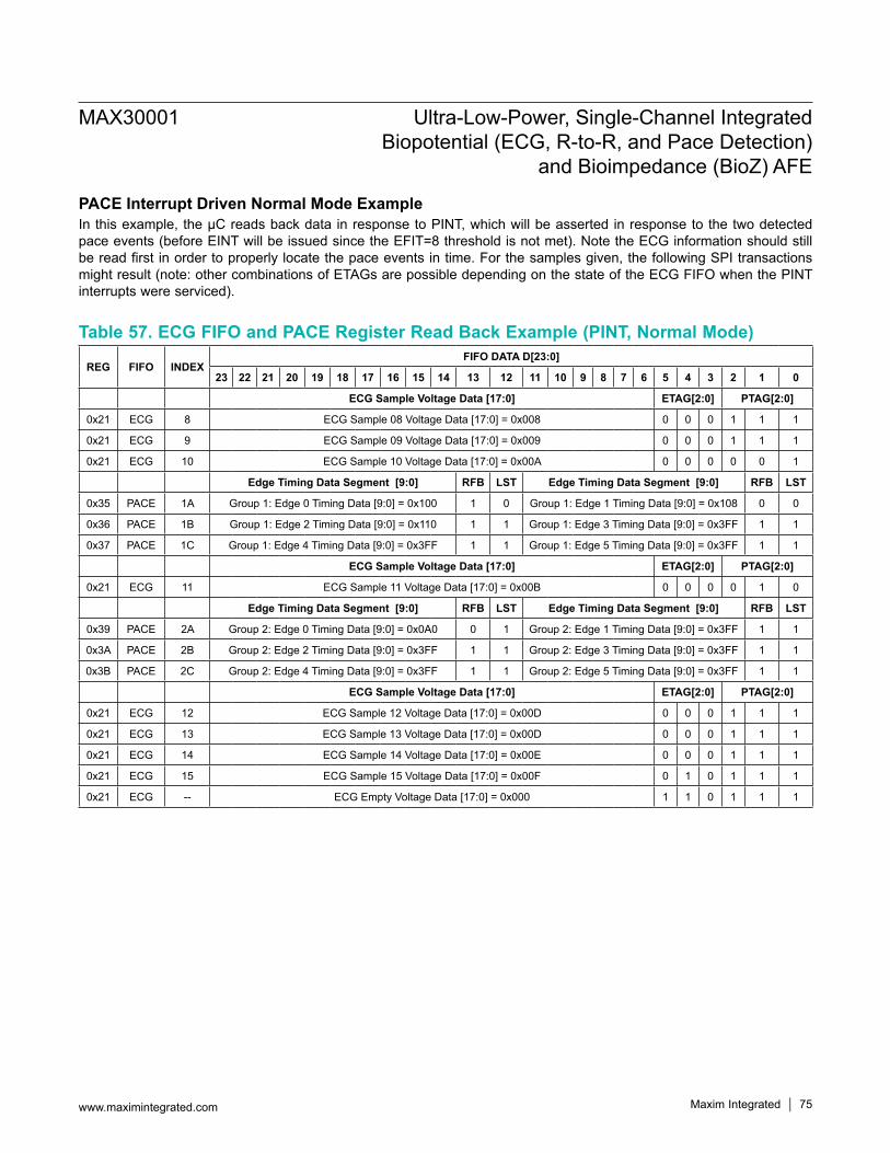
PACE Interrupt Driven Normal Mode ExampleIn this example, the µC reads back data in response to PINT, which will be asserted in response to the two detected pace events (before EINT will be issued since the EFIT=8 threshold is not met). Note the ECG information should still be read first in order to properly locate the pace events in time. For the samples given, the following SPI transactions might result (note: other combinations of ETAGs are possible depending on the state of the ECG FIFO when the PINT interrupts were serviced).
Table 57. ECG FIFO and PACE Register Read Back Example (PINT, Normal Mode)
REG FIFO INDEXFIFO DATA D[23:0]
23 22 21 20 19 18 17 16 15 14 13 12 11 10 9 8 7 6 5 4 3 2 1 0
ECG Sample Voltage Data [17:0] ETAG[2:0] PTAG[2:0]
0x21 ECG 8 ECG Sample 08 Voltage Data [17:0] = 0x008 0 0 0 1 1 1
0x21 ECG 9 ECG Sample 09 Voltage Data [17:0] = 0x009 0 0 0 1 1 1
0x21 ECG 10 ECG Sample 10 Voltage Data [17:0] = 0x00A 0 0 0 0 0 1
Edge Timing Data Segment [9:0] RFB LST Edge Timing Data Segment [9:0] RFB LST
0x35 PACE 1A Group 1: Edge 0 Timing Data [9:0] = 0x100 1 0 Group 1: Edge 1 Timing Data [9:0] = 0x108 0 0
0x36 PACE 1B Group 1: Edge 2 Timing Data [9:0] = 0x110 1 1 Group 1: Edge 3 Timing Data [9:0] = 0x3FF 1 1
0x37 PACE 1C Group 1: Edge 4 Timing Data [9:0] = 0x3FF 1 1 Group 1: Edge 5 Timing Data [9:0] = 0x3FF 1 1
ECG Sample Voltage Data [17:0] ETAG[2:0] PTAG[2:0]
0x21 ECG 11 ECG Sample 11 Voltage Data [17:0] = 0x00B 0 0 0 0 1 0
Edge Timing Data Segment [9:0] RFB LST Edge Timing Data Segment [9:0] RFB LST
0x39 PACE 2A Group 2: Edge 0 Timing Data [9:0] = 0x0A0 0 1 Group 2: Edge 1 Timing Data [9:0] = 0x3FF 1 1
0x3A PACE 2B Group 2: Edge 2 Timing Data [9:0] = 0x3FF 1 1 Group 2: Edge 3 Timing Data [9:0] = 0x3FF 1 1
0x3B PACE 2C Group 2: Edge 4 Timing Data [9:0] = 0x3FF 1 1 Group 2: Edge 5 Timing Data [9:0] = 0x3FF 1 1
ECG Sample Voltage Data [17:0] ETAG[2:0] PTAG[2:0]
0x21 ECG 12 ECG Sample 12 Voltage Data [17:0] = 0x00D 0 0 0 1 1 1
0x21 ECG 13 ECG Sample 13 Voltage Data [17:0] = 0x00D 0 0 0 1 1 1
0x21 ECG 14 ECG Sample 14 Voltage Data [17:0] = 0x00E 0 0 0 1 1 1
0x21 ECG 15 ECG Sample 15 Voltage Data [17:0] = 0x00F 0 1 0 1 1 1
0x21 ECG -- ECG Empty Voltage Data [17:0] = 0x000 1 1 0 1 1 1
MAX30001 Ultra-Low-Power, Single-Channel Integrated Biopotential (ECG, R-to-R, and Pace Detection)
and Bioimpedance (BioZ) AFE
www.maximintegrated.com Maxim Integrated 75

In the example above, the µC will read back complete and correct results but better use could be made of the ECG ETAG and pace information to realize more efficient µC communications as shown below.The example transactions above will read back identical results, but the efficiency is improved by only reading back loca-tions indicated by the ECG ETAG and PACE LST bits.
Table 58. ECG FIFO and PACE Register Read Back Example (PINT, Normal Mode, Reduced Transactions)
REG FIFO INDEXFIFO DATA D[23:0]
23 22 21 20 19 18 17 16 15 14 13 12 11 10 9 8 7 6 5 4 3 2 1 0
ECG Sample Voltage Data [17:0] ETAG[2:0] PTAG[2:0]
0x21 ECG 8 ECG Sample 08 Voltage Data [17:0] = 0x008 0 0 0 1 1 1
0x21 ECG 9 ECG Sample 09 Voltage Data [17:0] = 0x009 0 0 0 1 1 1
0x21 ECG 10 ECG Sample 10 Voltage Data [17:0] = 0x00A 0 0 0 0 0 1
Edge Timing Data Segment [9:0] RFB LST Edge Timing Data Segment [9:0] RFB LST
0x35 PACE 1A Group 1: Edge 0 Timing Data [9:0] = 0x100 1 0 Group 1: Edge 1 Timing Data [9:0] = 0x108 0 0
0x36 PACE 1B Group 1: Edge 2 Timing Data [9:0] = 0x110 1 1 Group 1: Edge 3 Timing Data [9:0] = 0x3FF 1 1
ECG Sample Voltage Data [17:0] ETAG[2:0] PTAG[2:0]
0x21 ECG 11 ECG Sample 11 Voltage Data [17:0] = 0x00B 0 0 0 0 1 0
Edge Timing Data Segment [9:0] RFB LST Edge Timing Data Segment [9:0] RFB LST
0x39 PACE 2A Group 2: Edge 0 Timing Data [9:0] = 0x0A0 0 1 Group 2: Edge 1 Timing Data [9:0] = 0x3FF 1 1
ECG Sample Voltage Data [17:0] ETAG[2:0] PTAG[2:0]
0x21 ECG 12 ECG Sample 12 Voltage Data [17:0] = 0x00C 0 0 0 1 1 1
0x21 ECG 13 ECG Sample 13 Voltage Data [17:0] = 0x00D 0 0 0 1 1 1
0x21 ECG 14 ECG Sample 14 Voltage Data [17:0] = 0x00E 0 0 0 1 1 1
0x21 ECG 15 ECG Sample 15 Voltage Data [17:0] = 0x00F 0 1 0 1 1 1
MAX30001 Ultra-Low-Power, Single-Channel Integrated Biopotential (ECG, R-to-R, and Pace Detection)
and Bioimpedance (BioZ) AFE
www.maximintegrated.com Maxim Integrated 76

Burst Mode ExampleIn this example, the µC reads data in response to the EINT bit and that EFIT = 8. For the samples given, the following Burst Mode SPI transactions might result.The example burst mode transactions below will read back complete and correct results. Note that to achieve this read back in burst mode only three commands are issued: ECG Burst 8 + (9 x 24) SCLK cycles, PACE Group 1 Burst 8 + (3 x 24) SCLK cycles, and PACE Group 2 Burst 8 + (3 x 24) SCLK cycles; however, better use could be made of the ECG ETAG and pace information to realize more efficient µC communications.
Table 59. ECG FIFO and PACE Register Read Back Example (EINT, Burst Mode)
REG FIFO INDEXFIFO DATA D[23:0]
23 22 21 20 19 18 17 16 15 14 13 12 11 10 9 8 7 6 5 4 3 2 1 0
ECG Sample Voltage Data [17:0] ETAG[2:0] PTAG[2:0]
0x20 ECG 8 ECG Sample 08 Voltage Data [17:0] = 0x008 0 0 0 1 1 1
ECG 9 ECG Sample 09 Voltage Data [17:0] = 0x009 0 0 0 1 1 1
ECG 10 ECG Sample 10 Voltage Data [17:0] = 0x00A 0 0 0 0 0 1
ECG 11 ECG Sample 11 Voltage Data [17:0] = 0x00B 0 0 0 0 1 0
ECG 12 ECG Sample 12 Voltage Data [17:0] = 0x00C 0 0 0 1 1 1
ECG 13 ECG Sample 13 Voltage Data [17:0] = 0x00D 0 0 0 1 1 1
ECG 14 ECG Sample 14 Voltage Data [17:0] = 0x00E 0 0 0 1 1 1
ECG 15 ECG Sample 15 Voltage Data [17:0] = 0x00F 0 1 0 1 1 1
ECG -- ECG Empty Voltage Data [17:0] = 0x000 1 1 0 1 1 1
23 22 21 20 19 18 17 16 15 14 13 12 11 10 9 8 7 6 5 4 3 2 1 0
Edge Timing Data Segment [9:0] RFB LST Edge Timing Data Segment [9:0] RFB LST
0x34 PACE 1A Group 1: Edge 0 Timing Data [9:0] = 0x100 1 0 Group 1: Edge 1 Timing Data [9:0] = 0x108 0 0
PACE 1B Group 1: Edge 2 Timing Data [9:0] = 0x110 1 1 Group 1: Edge 3 Timing Data [9:0] = 0x3FF 1 1
PACE 1C Group 1: Edge 4 Timing Data [9:0] = 0x3FF 1 1 Group 1: Edge 5 Timing Data [9:0] = 0x3FF 1 1
0x38 PACE 2A Group 2: Edge 0 Timing Data [9:0] = 0x0A0 0 1 Group 2: Edge 1 Timing Data [9:0] = 0x3FF 1 1
PACE 2B Group 2: Edge 2 Timing Data [9:0] = 0x3FF 1 1 Group 2: Edge 3 Timing Data [9:0] = 0x3FF 1 1
PACE 2C Group 2: Edge 4 Timing Data [9:0] = 0x3FF 1 1 Group 2: Edge 5 Timing Data [9:0] = 0x3FF 1 1
MAX30001 Ultra-Low-Power, Single-Channel Integrated Biopotential (ECG, R-to-R, and Pace Detection)
and Bioimpedance (BioZ) AFE
www.maximintegrated.com Maxim Integrated 77

The example burst mode transactions below will read back identical results, but the efficiency is improved by only read-ing back locations indicated by the ECG ETAG and PACE LST bits. To achieve this read back in burst mode only three commands are issued: ECG Burst 8 + (8 x 24) SCLK cycles, PACE Group 1 Burst 8 + (2 x 24) SCLK cycles, and PACE Group 2 Burst 8 + 24 SCLK cycles.
Table 60. ECG FIFO and PACE Register Read Back Example (EINT, Burst Mode, Reduced Transactions)
REG FIFO INDEXFIFO DATA (D[23:0])
23 22 21 20 19 18 17 16 15 14 13 12 11 10 9 8 7 6 5 4 3 2 1 0
ECG Sample Voltage Data [17:0] ETAG[2:0] PTAG[2:0]
0x20 ECG 8 ECG Sample 08 Voltage Data [17:0] = 0x008 0 0 0 1 1 1
ECG 9 ECG Sample 09 Voltage Data [17:0] = 0x009 0 0 0 1 1 1
ECG 10 ECG Sample 10 Voltage Data [17:0] = 0x00A 0 0 0 0 0 1
ECG 11 ECG Sample 11 Voltage Data [17:0] = 0x00B 0 0 0 0 1 0
ECG 12 ECG Sample 12 Voltage Data [17:0] = 0x00C 0 0 0 1 1 1
ECG 13 ECG Sample 13 Voltage Data [17:0] = 0x00D 0 0 0 1 1 1
ECG 14 ECG Sample 14 Voltage Data [17:0] = 0x00E 0 0 0 1 1 1
ECG 15 ECG Sample 15 Voltage Data [17:0] = 0x00F 0 1 0 1 1 1
23 22 21 20 19 18 17 16 15 14 13 12 11 10 9 8 7 6 5 4 3 2 1 0
Edge Timing Data Segment [9:0] RFB LST Edge Timing Data Segment [9:0] RFB LST
0x34 PACE 1A Group 1: Edge 0 Timing Data [9:0] = 0x100 1 0 Group 1: Edge 1 Timing Data [9:0] = 0x108 0 0
PACE 1B Group 1: Edge 2 Timing Data [9:0] = 0x110 1 1 Group 1: Edge 3 Timing Data [9:0] = 0x3FF 1 1
0x38 PACE 2A Group 2: Edge 0 Timing Data [9:0] = 0x0A0 0 1 Group 2: Edge 1 Timing Data [9:0] = 0x3FF 1 1
MAX30001 Ultra-Low-Power, Single-Channel Integrated Biopotential (ECG, R-to-R, and Pace Detection)
and Bioimpedance (BioZ) AFE
www.maximintegrated.com Maxim Integrated 78

Resulting Data Record ExampleIn this example, the µC reads data in response to EINT and that EFIT=8. For the complete FIFO samples given and the resulting two interrupts, the following SPI transactions might have resulted (starting from the beginning of the FIFO record).
Table 61. Complete Read Back Example (EINT, Normal Mode)
REG FIFO INDEXFIFO DATA (D[23:0])
23 22 21 20 19 18 17 16 15 14 13 12 11 10 9 8 7 6 5 4 3 2 1 0ECG Sample Voltage Data [17:0] ETAG[2:0] PTAG[2:0]
0x21 ECG 0 ECG Sample 00 Voltage Data [17:0] = 0x000 0 0 1 1 1 1
0x21 ECG 1 ECG Sample 01 Voltage Data [17:0] = 0x001 0 0 1 1 1 1
0x21 ECG 2 ECG Sample 02 Voltage Data [17:0] = 0x002 0 0 0 1 1 1
0x21 ECG 3 ECG Sample 03 Voltage Data [17:0] = 0x003 0 0 0 1 1 1
0x21 ECG 4 ECG Sample 04 Voltage Data [17:0] = 0x004 0 0 0 1 1 1
0x21 ECG 5 ECG Sample 05 Voltage Data [17:0] = 0x005 0 0 0 0 0 0
0x21 ECG 6 ECG Sample 06 Voltage Data [17:0] = 0x006 0 0 0 1 1 1
0x21 ECG 7 ECG Sample 07 Voltage Data [17:0] = 0x007 0 1 0 1 1 1
0x21 ECG -- ECG Empty Voltage Data [17:0] = 0x000 1 1 0 1 1 1
Edge Timing Data Segment [9:0] RFB LST Edge Timing Data Segment [9:0] RFB LST0x31 PACE 0A Group 0: Edge 0 Timing Data [9:0] = 0x000 1 0 Group 0: Edge 1 Timing Data [9:0] = 0x011 0 0
0x32 PACE 0B Group 0: Edge 2 Timing Data [9:0] = 0x022 1 0 Group 0: Edge 3 Timing Data [9:0] = 0x033 0 1
0x33 PACE 0C Group 0: Edge 4 Timing Data [9:0] = 0x3FF 1 1 Group 0: Edge 5 Timing Data [9:0] = 0x3FF 1 1
ECG Sample Voltage Data [17:0] ETAG[2:0] PTAG[2:0]0x21 ECG 8 ECG Sample 08 Voltage Data [17:0] = 0x008 0 0 0 1 1 1
0x21 ECG 9 ECG Sample 09 Voltage Data [17:0] = 0x009 0 0 0 1 1 1
0x21 ECG 10 ECG Sample 10 Voltage Data [17:0] = 0x00A 0 0 0 0 0 1
0x21 ECG 11 ECG Sample 11 Voltage Data [17:0] = 0x00B 0 0 0 0 1 0
0x21 ECG 12 ECG Sample 12 Voltage Data [17:0] = 0x00C 0 0 0 1 1 1
0x21 ECG 13 ECG Sample 13 Voltage Data [17:0] = 0x00D 0 0 0 1 1 1
0x21 ECG 14 ECG Sample 14 Voltage Data [17:0] = 0x00E 0 0 0 1 1 1
0x21 ECG 15 ECG Sample 15 Voltage Data [17:0] = 0x00F 0 1 0 1 1 1
0x21 ECG -- ECG Empty Voltage Data [17:0] = 0x000 1 1 0 1 1 1
Edge Timing Data Segment [9:0] RFB LST Edge Timing Data Segment [9:0] RFB LST0x35 PACE 1A Group 1: Edge 0 Timing Data [9:0] = 0x100 1 0 Group 1: Edge 1 Timing Data [9:0] = 0x108 0 0
0x36 PACE 1B Group 1: Edge 2 Timing Data [9:0] = 0x110 1 1 Group 1: Edge 3 Timing Data [9:0] = 0x3FF 1 1
0x37 PACE 1C Group 1: Edge 4 Timing Data [9:0] = 0x3FF 1 1 Group 1: Edge 5 Timing Data [9:0] = 0x3FF 1 1
0x39 PACE 2A Group 2: Edge 0 Timing Data [9:0] = 0x0A0 0 1 Group 2: Edge 1 Timing Data [9:0] = 0x3FF 1 1
0x3A PACE 2B Group 2: Edge 2 Timing Data [9:0] = 0x3FF 1 1 Group 2: Edge 3 Timing Data [9:0] = 0x3FF 1 1
0x3B PACE 2C Group 2: Edge 4 Timing Data [9:0] = 0x3FF 1 1 Group 2: Edge 5 Timing Data [9:0] = 0x3FF 1 1
MAX30001 Ultra-Low-Power, Single-Channel Integrated Biopotential (ECG, R-to-R, and Pace Detection)
and Bioimpedance (BioZ) AFE
www.maximintegrated.com Maxim Integrated 79

The µC must now prepare a complete record of the ECG waveform given the data observed thus far. All empty samples, which do not represent valid ECG time steps or valid pace edges, will be filtered out. Then the pace edges will be interleaved within the appropriate ECG sample intervals. For purposes of this example, assume
FMSTR[1:0] = 01 and ECG_RATE[1:0] = 10 (in CNFG_GEN and CNFG_ECG registers, respectively), thus:
FECG = 125spsTECG = 1/FECG = 8ms
FPACE = 64,000HzPACE_RES = 1/ FPACE = 15.625µs
Table 62. Example Post-Processed ECG and PACE Record TIME (ms)
VOLTAGE (LSBs) F* C** P*** NOTE
0.000 0x000 FAST mode engaged – ECG voltage may be invalid
8.000 0x001 FAST mode engaged – ECG voltage may be invalid
16.000 0x002
24.000 0x003
32.000 0x004
40.000 0x005 Pace edge(s) detected during current sample interval - ECG voltage may be impacted
40.000 ↑ Pace rising edge detected ( 0*15.625µs = 0.000ms delayed)
40.266 ↓ Pace falling edge detected (17*15.625µs = 0.256ms delayed)
40.531 ↑ Pace rising edge detected (34*15.625µs = 0.531ms delayed)
40.797 ↓ Pace falling edge detected (51*15.625µs = 0.797ms delayed)
48.000 0x006 Pace edge(s) detected during preceding sample interval - ECG voltage may be impacted
56.000 0x007
64.000 0x008
72.000 0x009
80.000 0x00A Pace edge(s) detected during current sample interval - ECG voltage may be impacted
84.000 ↑ Pace rising edge detected (256*15.625µs = 4.000ms delayed)
84.125 ↓ Pace falling edge detected (264*15.625µs = 4.125ms delayed)
84.250 ↑ Pace rising edge detected (272*15.625µs = 4.250ms delayed)
88.000 0x00B Pace edge(s) detected during preceding & current sample interval - ECG voltage may be impacted
90.500 ↓ Pace falling edge detected (160*15.625µs = 2.500ms delayed)
96.000 0x00C Pace edge(s) detected during preceding sample interval - ECG voltage may be impacted
104.000 0x00D
112.000 0x00E
120.000 0x00F*F = Fast mode**C = Sample corrupted by Pace activity***P = Pace edge
MAX30001 Ultra-Low-Power, Single-Channel Integrated Biopotential (ECG, R-to-R, and Pace Detection)
and Bioimpedance (BioZ) AFE
www.maximintegrated.com Maxim Integrated 80

Figure 17a. Two-Electrode ECG and Respiration Monitor Typical Application Circuit
ECGP
ECGN
CAPP
CAPN
MAX30001
DGNDAGND
CSB
SDI
SCLK
SDO
INTB
INT2B
FCLK
MCU
CSB
MOSI
SCLK
MISO
INTB
INT2B
FCLK
VCM VBG VREF
DRVP
DRVN
RBIAS
10µF 1µF 10µF
AOUT
324kΩ CPLL
1nF47nF
47nF
1µF
200kΩ
200kΩ
2nF
10pF
ELECTRODES
10pF
200Ω
200Ω
47pF
10pF
10pF
BIP
BIN
AVDD DVDD OVDD
0.1µF10µF0.1µF10µF
1.1V to 2.0V 1.65V to 3.6V
Typical Application Circuits
MAX30001 Ultra-Low-Power, Single-Channel Integrated Biopotential (ECG, R-to-R, and Pace Detection)
and Bioimpedance (BioZ) AFE
www.maximintegrated.com Maxim Integrated 81

Figure 17b. Four-Electrode ECG and Respiration Monitor Typical Application Circuit
ECGP
ECGN
CAPP
CAPN
MAX30001
DGNDAGND
CSB
SDI
SCLK
SDO
INTB
INT2B
FCLK
MCU
CSB
MOSI
SCLK
MISO
INTB
INT2B
FCLK
VCM VBG VREF
DRVP
DRVN
RBIAS
10µF 1µF 10µF
AOUT
324kΩ CPLL
1nF47nF
47nF
1µF
200kΩ
200kΩ
2nF
10pF
ELECTRODES
10pF
200Ω
200Ω
47pF
10pF
10pF
BIP
BIN
AVDD DVDD OVDD
0.1µF10µF0.1µF10µF
1.1V to 2.0V 1.65V to 3.6V
Typical Application Circuits (continued)
MAX30001 Ultra-Low-Power, Single-Channel Integrated Biopotential (ECG, R-to-R, and Pace Detection)
and Bioimpedance (BioZ) AFE
www.maximintegrated.com Maxim Integrated 82

Application DiagramsSee Figure 18 for an example of a clinical application for monitoring ECG and respiration using just two electrodes and with optional shared defibrillation protection circuitry. The electrode models are shown to illustrate the electrical characteristics of the physical electrodes.
Four Electrode ECG and Respiration Monitoring ApplicationSee Figure 19 for an example of a clinical application for monitoring ECG and respiration using four electrodes and with optional defibrillation protection circuitry. The electrode models are shown to illustrate the electrical characteristics of the physical electrodes.
Figure 18. Two Electrode ECG and Respiration Monitoring with Optional Common Defibrillation Protection.
MAX30001PHYSICALELECTRODES
PCB
ELECTRODE MODELSRBODYOPTIONALDEFIBPROTECTION
ECGP
ECGN
CAPP
CAPN
DRVP
DRVN
BIP
BIN
EXTERNAL EMI FILTERS
MAX30001 Ultra-Low-Power, Single-Channel Integrated Biopotential (ECG, R-to-R, and Pace Detection)
and Bioimpedance (BioZ) AFE
www.maximintegrated.com Maxim Integrated 83

Figure 19. Four Electrode ECG and Respiration Monitoring with Optional Defibrillation Protection.
MAX30001PHYSICALELECTRODES
PCB
ELECTRODE MODELSRBODY
OPTIONALDEFIBPROTECTION
ECGP
ECGN
CAPP
CAPN
DRVP
DRVN
BIP
BIN
EXTERNAL EMI FILTERS
MAX30001 Ultra-Low-Power, Single-Channel Integrated Biopotential (ECG, R-to-R, and Pace Detection)
and Bioimpedance (BioZ) AFE
www.maximintegrated.com Maxim Integrated 84

+Denotes lead(Pb)-free/RoHS-compliant package. T = Tape and reel. *Future product. Contact factory for availability. **EP = Exposed pad.
PART TEMP RANGE PIN-PACKAGEMAX30001CTI+* 0ºC TO +70ºC 28 TQFN-EP**
MAX30001CTI+T* 0ºC TO +70ºC 28 TQFN-EP**
MAX30001CWV+ 0ºC TO +70ºC 30WLP
MAX30001CWV+T 0ºC TO +70ºC 30WLP PACKAGE TYPE
PACKAGE CODE
OUTLINE NO.
LAND PATTERN NO.
28-TQFN T2855+8 21-0140 90-0028
30 WLP W302L2+1 21-100074Refer to
Application Note 1891
Ordering Information
Chip InformationPROCESS: CMOS
Package InformationFor the latest package outline information and land patterns (footprints), go to www.maximintegrated.com/packages. Note that a “+”, “#”, or “-” in the package code indicates RoHS status only. Package drawings may show a different suffix character, but the drawing pertains to the package regardless of RoHS status.
MAX30001 Ultra-Low-Power, Single-Channel Integrated Biopotential (ECG, R-to-R, and Pace Detection)
and Bioimpedance (BioZ) AFE
www.maximintegrated.com Maxim Integrated 85

REVISIONNUMBER
REVISIONDATE DESCRIPTION PAGES
CHANGED
0 8/17 Initial release —
1 9/17 Added figures and updated tables 1–86
Revision History
Maxim Integrated cannot assume responsibility for use of any circuitry other than circuitry entirely embodied in a Maxim Integrated product. No circuit patent licenses are implied. Maxim Integrated reserves the right to change the circuitry and specifications without notice at any time. The parametric values (min and max limits) shown in the Electrical Characteristics table are guaranteed. Other parametric values quoted in this data sheet are provided for guidance.
Maxim Integrated and the Maxim Integrated logo are trademarks of Maxim Integrated Products, Inc.
MAX30001 Ultra-Low-Power, Single-Channel Integrated Biopotential (ECG, R-to-R, and Pace Detection)
and Bioimpedance (BioZ) AFE
© 2017 Maxim Integrated Products, Inc. 86
For pricing, delivery, and ordering information, please contact Maxim Direct at 1-888-629-4642, or visit Maxim Integrated’s website at www.maximintegrated.com.