max38801 evaluation kit - evaluates: max38801 · reliable power delivery solution for low-output...
TRANSCRIPT

Evaluates: MAX38801MAX38801 Evaluation Kit
General DescriptionThe MAX38801 evaluation kit (EV kit) serves as a reference platform for evaluating the MAX38801 voltage regulator IC. This single-chip, integrated switching regulator provides an extremely compact, highly efficient, fast, accurate, and reliable power delivery solution for low-output voltage applications. The MAX38801 has different programmability options to enable a wide range of configurations.The EV kit consists of a fully-assembled and tested Printed Circuit Board (PCB) implementation of the MAX38801. Jumpers, test points and input/output connectors are included for flexibility and ease-of-use. Refer to the data sheet for ordering information and more details.
Applications Servers/µServers I/O and Chipset Supplies GPU Core Supply DDR Memory—VDDQ and VTT Point-of-Load (PoL) Applications
Features High-Efficiency Solution
• Up to 96% Peak• Up to 92% Full-Load• Up to 94% Light-Load Efficiency at 1A with DCM
Enabled Inductor Valley Current Limit is Configured to 12A
(R_SEL = R1 = 46.4kΩ) Programmable Switching Frequency from 400kHz
to 900kHz Programmable Positive and Negative OCP Limit Programmable Reference Voltage with External
Input Option Fast Transient Response with Quick PWM™
Architecture Differential Remote Sense with Open-Circuit
Detection Percentage-Based Output Power Good and OVP Open-Drain Status Indicator (STAT) Pin Input Undervoltage and Overvoltage Lockout Adaptive Dead Time Control Integrated Boost Switch 19-Bump WLCSP (2.2mm x 2.8mm) Footprint Operation Using Ceramic Input and Output
Capacitors
319-100062; Rev 0; 8/17
Ordering Information appears at end of data sheet.
Quick PWM is a trademark of Maxim Integrated Products, Inc.
Maxim Integrated 2www.maximintegrated.com
Evaluates: MAX38801MAX38801 Evaluation Kit
Quick StartRequired Equipment
MAX38801 EV kit 12V, 10A DC power supply Load capable of sinking 12A Digital voltmeter Oscilloscope
ProcedureThe EV kit is fully assembled and tested. Follow the steps below to verify the board operation. Caution: Do not turn on power supply until all connections are completed.1) Connect a 12V power supply to the VDD1 and GND1
banana jacks.2) Make sure the shunt is installed on:
a) J16 (1-2) to close the sense line.b) J4 (1-2) to power up the on-board LDO which
regulates 1.8V.c) J12 (1-2) to provide the 1.8V bias supply to the
regulator from the on-board LDO.d) J15 (3-5) to pull up the STAT pin.e) J15 (4-6) to pull up the OE pin.
3) Connect a voltmeter to the VOUT and GND banana jacks (J8, J11, J13, and J14 can be used as well).
4) Turn on the power supply.5) Verify that the voltmeter reads 1.05V.
Detailed Description of HardwareThe MAX38801 provides compact high-efficiency power delivery for precision outputs that demand fast transient response. The 19-ball (2.2mm x 2.8mm) CSP package mini-mizes the PCB area. The EV kit is preset for 1.05V output and can provide up to 12A from a 6.5V to 14V input supply.
Bias SupplyThe MAX38801 EV kit has an on-board LDO (U2) that can provide the required 1.8V VCC bias voltage to the regulator as well as the pull up voltage for the Output Enable (OE) input. This allows testing the part using a single external power supply. To enable the on-board LDO install the shunt on jumper J4. To effectively use the LDO to supply the VCC bias voltage to the regulator also install the shunt on jumper J12.In order to properly measure the efficiency of the regulator, the LDO should not be active. To disable it, both the shunts on J4 and J12 need to be removed. An external 1.8V, 0.1A current limited power supply needs to be
connected between J12-2 and ground. The same signal should be connected to J10 (1-2) to pull up the OE pin.
Regulator enableTo enable the regulator, OE pin needs to be pulled high. If the on-board 1.8V LDO is active (the shunt on jumper J4 is in place), the output voltage can be used for the pur-pose. Installing a shunt on J15 (4-6) pulls the OE signal high to 1.8V through a 20kΩ resistor. To shut down the regulator a shunt needs to be installed on J10. This forces the OE pin low.
Status PinThe MAX38801 has an open collector status (STAT) output to report fault or output under voltage event. Install a shunt on J15 (3-5) to pull up this pin to VCC through a 20kΩ resistor. Since STAT pin is 3.3V tolerant, a shunt on J15 (1-3) can be installed to pull up this pin through a 20kΩ resistor to the 3.3V provided by the on board regulator U3 (install a shunt on J5 (3-4) to enable the LDO).
Scenario SelectionSeveral parameters of the MAX38801 can be programmed to allow optimization for specific applications. By selecting the appropriate value of resistor R_SEL (R1) and capacitor C_SEL (C4), the optimum set of parameters (scenario) can be programmed. While R_SEL selects the proper scenario, C_SEL determines the nominal FSW. The MAX38801 features a configuration table to provide a wide range of options. Table 1 shows the scenario table for MAX38801.

Maxim Integrated 3www.maximintegrated.com
Evaluates: MAX38801MAX38801 Evaluation Kit
Setting the Output VoltageThe output voltage of MAX38801 depends both on the reference voltage (VREF) and the resistor divider ratio.Equation 1
= × +
6OUT REF
9
RV V 1
R
The reference voltage is selected through RSEL (see Table 1 ) and can be either internal or external (refer to the data sheet for more details). In order to optimize the common mode rejection of the error amplifier, choose the voltage divider resistors so that their parallel resistance RPAR is as close as possible to 2kΩ.Equation 2
= ×
= × −
PAR6 OUT
REF
PAR9
6 PAR
RR V
V
RR R6
R R
where,R6 = Top divider resistorR9 = Bottom divider resistorRPAR = Desired parallel resistance of R6 and R9VOUT = Output voltageVREF = Reference voltage
Operation with External VREFWhen using an external reference adopt the configuration shown in Figure 1. Once OE is asserted, the regulator briefly discharges the SENSE- node and releases it as regulation begins. In this case, the soft-start ramp is determined by the external low-pass filter time constant. The external filter time constant needs to be lower than TSS/3 in order to avoid premature assertion of STAT pin while the output voltage is still ramping.The external reference voltage can be applied prior to enabling the regulator, or ramped up right after enable is asserted. In both cases, the low-pass filtered reference voltage at SENSE- pin must reach its final value within TSS.Typical values for the filter components are:
RF = 2.2kΩ CF = 0.22μF
Table 1. MAX38801 Configuration Table
R_SEL (kΩ)
VREF (V)
SOFT-START
TIME (TSS) (ms)
VALLEY OCP
INCEPTION (A)
OPERATION MODES
REPORTING (CURRENT/
TEMP)
RSENSE (GAIN) (MΩ)
FSW (kHz)TSTAT
(µs)C_SEL
0pF 200 pF
820 pF
1.78
0.95
612 CCM
Current2.1
700 800 900 2000
2.67 15 CCM/DCM
4.02
3
12 CCM
6.04 15 CCM/DCM
9.09Ext. 12 CCM
13.3 1.5
20.0
0.6 6
18CCM/DCM
30.9CCM
46.4
1271.5CCM/DCM
Temp
107 Current 1.05
162 Ext. 1.5 15 CCM Temp 2.1 400 500 600 128

Maxim Integrated 4www.maximintegrated.com
Evaluates: MAX38801MAX38801 Evaluation Kit
Input Voltage MonitoringVDD1 and GND1 sense points as well as J3 can be used to monitor the input supply.
Output Voltage MonitoringJ11 and J13 monitor the output voltage. These test points should not be used for loading. Use scopejack J14 to monitor the output voltage ripple on an oscilloscope.
Efficiency MeasurementThe following steps describe how to measure the regulator efficiency.1) Connect a 12V power supply to the VDD1 and GND1
banana jacks. To avoid the input voltage to drop at high load due to power losses on connection cables connect the sense lines of the power supply to VDD1 and GND1 headers.
2) Connect an external 1.8V, 0.1A current limited power supply between J12-2 and ground
3) Connect the same power supply to J10-1 to enable the regulator.
4) Connect a load to the VOUT and GND banana jacks for better results. J8 can also be used for low currents.
5) Make sure the shunt is installed on J16 (1-2) to close the sense line
6) Remove all the other jumpers.7) Connect a voltmeter to J11 or J13.8) Turn on the power supply.9) Measure VIN, IIN, VOUT, IOUT, VBIAS, and IBIAS.10) Calculate the efficiency as:Equation 3
( )OUT OUT
IN IN BIAS BIAS
V IV I ( V I )
×η= × + ×
Figure 1. Electrical Connections to Use the External Voltage Reference Feature.
RSTAT
CVCC CIN
CBST
R_SELC_SEL
VCC VDDH
STAT
OE
AGNDPGM
GND
SENSE-
SENSE+
VX
BSTMAX38801
ROE
RFB1
RFB2
RF
CF
LOUT
COUT
VCC VDDH
VOUT
VREF
Kelvin Connection to Load

Maxim Integrated 5www.maximintegrated.com
Evaluates: MAX38801MAX38801 Evaluation Kit
MAX38801 EV Kit Bill of MaterialsITEM REF_DES DNI/DNP QTY MFG PART # MANUFACTURER VALUE DESCRIPTION
1 C1, C2 - 2 TPSE157M016R0100 AVX 150µF CAPACITOR; SMT; 7343; TANTALUM; 150µF;16V; 20%; TPS; -55°C to +125°C
2 C3 - 1
C0402X7R160-104KNE;CL05B104KO5NNNC;GRM155R71C104KA88;C1005X7R1C104K;CC0402KRX7R7BB104;EMK105B7104KV
VENKEL LTD./SAMSUNG ELECTRONICS/MURATA/TDK/YAGEO PHICOMP/
TAIYO YUDEN0.1µF CAPACITOR; SMT (0402); CERAMIC CHIP;
0.1µF; 16V; TOL = 10%; TG = -55°C TO +125°C; TC = X7R;
3 C4 - 1 ECJ-0EB1E821K PANASONIC 820PF CAPACITOR; SMT (0402); CERAMIC CHIP; 820PF; 25V; TOL = 10%;MODEL = ECJ SERIES; TG = -55°C TO +125°C; TC = X7R
4 C5, C6, C10, C11 - 4 C3216X7R1C106M160AC TDK 10µF CAPACITOR; SMT (1206); CERAMIC CHIP; 10µF; 16V; TOL = 20%;MODEL = C SERIES; TG =-55°C TO +125°C; TC = X7R
5 C7, C21, C54 - 3 EMK107B7105MA TAIYO YUDEN 1µF CAPACITOR; SMT (0603); CERAMIC CHIP; 1µF; 16V; TOL = 20%;MODEL = M SERIES; TG = -55°C TO +125°C; TC = X7R
6 C8 - 1 GRM188R71E474KA12 MURATA 0.47µF CAPACITOR; SMT (0603); CERAMIC CHIP; 0.47µF; 25V;TOL = 10%; MODEL = GRM SERIES; TG = -55°C TO +125°C; TC = X7R
7 C9, C55 - 2 JMK105BBJ475MV-F;C1005X5R0J475M050BC TAIYO YUDEN; TDK 4.7µF CAPACITOR; SMT (0402); CERAMIC CHIP; 4.7µF; 6.3V; TOL = 20%;
TG = -55°C TO +85°C; TC = X5R
8 C12, C15, C16, C20, C34, C42, C44 - 7
C0805C226M9PAC;GRM21BR60J226ME39;JMK212BJ226MG;CL21A226MQCLQN
GENERIC PART 22µF CAPACITOR; SMT (0805); CERAMIC CHIP; 22µF; 6.3V;TOL = 20%; TG = -55°C TO +125°C; TC = X5R
9 C13, C14, C17-C19, C41, C46, C50 - 8 C2012X6S0J226M125AB;
GRM21BC80J TDK/MURATA 22µF CAPACITOR; SMT (0805); CERAMIC CHIP; 22µF; 6.3V;TOL = 20%; TG = -55°C TO +105°C; TC = X6S
10 C24 - 1C0402C103K3RAC;GRM155R71E103KA01D;C1005X7R1E103K
KEMET; MURATA; TDK 0.01µF CAPACITOR; SMT (0402); CERAMIC CHIP; 0.01µF; 25V;TOL = 10%; TG = -55°C TO +125°C; TC = X7R;
11 C25, C56 - 2 C0402X7R250-153KNE;GRM155R71E153KA61 VENKEL LTD./MURATA 0.015µF CAPACITOR; SMT (0402); CERAMIC CHIP; 0.015µF; 25V;
TOL = 10%; TG = -55°C TO +125°C; TC = X7R
12 C36 - 1
C0402X5R6R3-105KNP;C1005X5R0J105K;GRM155R60J105KE19;JMK105BJ105KV
VENKEL LTD./TDK/MURATA 1µF CAPACITOR; SMT (0402); CERAMIC CHIP; 1µF; 6.3V;TOL = 10%; TG = -55°C TO +85°C; TC = X5R;
13 C37 - 1 C1005X7R1H682K TDK 6800PF CAPACITOR; SMT (0402); CERAMIC CHIP; 6800PF; 50V;TOL = 10%; MODEL = C SERIES; TG = -55°C TO +125°C; TC = X7R
14 C38 - 1 C0402C153K4RAC;GRM155R71C153KA01 KEMET; MURATA 0.015µF CAPACITOR; SMT (0402); CERAMIC CHIP; 0.015µF; 16V;
TOL = 10%; TG = -55°C TO +125°C; TC = X7R
15 C39 - 1 C1005X7R1H222K050BA TDK 2200PF CAPACITOR; SMT (0402); CERAMIC CHIP; 2200PF; 50V; TOL = 10%;MODEL = C SERIES; TG = -55°C TO +125°C; TC = X7R
16 D1 - 1 2EZ15D5 MICRO COMMERCIAL COMPONENTS 15V DIODE; ZNR; THROUGH HOLE-AXIAL LEAD (DO-41); VZ = 15V; IZ = 0.122A
17 TP1-TP3, GND1, VDD1, VOUT - 6 108-0740-001 EMERSON NETWORK POWER 108-0740-001 CONNECTOR; MALE; PANELMOUNT; BANANA JACK; STRAIGHT; 1PIN
18J9, VX1, GND2,
GND1_HEADER,VDD1_HEADER
- 5 PEC01SAAN SULLINS ELECTRONICS CORP PEC01SAAN CONNECTOR; MALE; THROUGH HOLE; BREAKAWAY; STRAIGHT; 1PIN
19
J2, J6, GND_MAXIMPAD,GND1_MAXIMPAD,VDD1_MAXIMPAD,VOUT_MAXIMPAD
- 6 MAXIMPAD N/A MAXIMPAD EVK KIT PARTS; MAXIM PAD; NO WIRE TO BE SOLDERED ON THE MAXIMPAD
20 J1, J4, J10-J13, J16 - 7 PEC02SAAN SULLINS PEC02SAAN CONNECTOR; MALE; THROUGH HOLE; BREAKAWAY; STRAIGHT; 2PINS

Maxim Integrated 6www.maximintegrated.com
Evaluates: MAX38801MAX38801 Evaluation Kit
MAX38801 EV Kit Bill of Materials (continued)ITEM REF_DES DNI/DNP QTY MFG PART # MANUFACTURER VALUE DESCRIPTION
21 J3, J14 - 2 SCOPE_PROBE_JACK MAXIM SCOPE_PROBE_JACK EVKIT PART-SCOPE_PROBE_JACK
22 J5, J15 - 2 PEC03DAAN SULLINS ELECTRONICS CORP. PEC03DAAN CONNECTOR; MALE; THROUGH HOLE; BREAKAWAY; STRAIGHT THROUGH; 6PINS; -65°C TO +125°C
23 J7 - 1 PEC04SAAN SULLINS ELECTRONICS CORP. PEC04SAAN CONNECTOR; MALE; THROUGH HOLE; BREAKAWAY; STRAIGHT; 4PINS
24 J8 - 1 ED120/2DS ON-SHORE TECHNOLOGY INC. ED120/2DS CONNECTOR; FEMALE; THROUGH HOLE;BLUE TERMINAL BLOCK; STRAIGHT; 2PINS
25 L1 - 1 PCMC063T-R20MN SUSUMU CO LTD PCMC063T-R20MN INDUCTOR; SMT; CHOKE; TOL = ±20%; 24A;
26 L1 - 0 7.44373E+11 WURTH ELECTRONICS INC 7.44373E+11 INDUCTOR; SMT; SHIELDED; 0.22µH; TOL = ±30%; 15A;
27 R1 - 1 CR0402-16W-4642FT;CRCW040246K4FK VENKEL LTD./VISHAY DALE 46.4K RESISTOR; 0402; 46.4KΩ; 1%; 100PPM; 0.063W; THICK FILM
28 R2, R3 - 2 CRG0402F10K TE CONNECTIVITY 10K RESISTOR; 0402; 10KΩ; 1%; 100PPM; 0.063W; THICK FILM
29 R4, R7, R11,R15, R16 - 5 RC0402JR-070RL;
CR0402-16W-000RJT YAGEO PHYCOMP/VENKEL LTD. 0 RESISTOR; 0402; 0Ω; 5%; JUMPER; 0.063W; THICK FILM
30 R5, R8, R12 - 3 ERJ-2GEJ203X PANASONIC 20K RESISTOR; 0402; 20KΩ; 5%; 200PPM; 0.10W; THICK FILM
31 R6, R13 - 2 CRCW04022K10FK VISHAY DALE 2.1K RESISTOR; 0402; 2.1K; 1%; 100PPM; 0.0625W; THICK FILM
32 R9 - 1 ERA-2AEB2801X PANASONIC 2.8K RESISTOR; 0402; 2.8KΩ; 0.1%; 25PPM; 0.063W; METAL FILM
33 R10 - 1 CRCW04021K00JK VISHAY DALE 1K RESISTOR; 0402; 1KΩ; 5%; 100PPM; 0.063W; METAL FILM
34 R14 - 1 RCC-0402PW200RF INTERNATIONALMANUFACTURING SERVICE 200 RESISTOR; 0402; 200Ω; 1%; 100PPM; 0.080W; THICK FILM
35 SU1-SU5 - 5 STC02SYAN SULLINS ELECTRONICS CORP. STC02SYANTEST POINT; JUMPER; STR; TOTAL LENGTH = 0.256IN;BLACK; INSULATION=PBT CONTACT=PHOSPHOR BRONZE;COPPER PLATED TIN OVERALL
36 U1 - 1 MAX38801HCS+ MAXIM MAX38801HCS+ EVKIT PART-IC; VREG; INTEGRATED; STEP-DOWN SWITCHING REGULATOR WITH SELECTABLE APPLICATION CONFIGURATION; CSP19
37 U2 - 1 LP2992AIM5-1.8/NOPB TEXAS INSTRUMENTS LP2992AIM5-1.8/NOPB IC; VREG; MICROPOWER 250-mA LOW-NOISE ULTRALOW-DROPOUT REGULATOR DESIGNED FOR USE WITH VERY LOW-ESR OUTPUT CAPACITOR; SOT23-5
38 U3 - 1 LP2992AIM5-3.3/NOPB TEXAS INSTRUMENTS LP2992AIM5-3.3/NOPB IC; VREG; MICROPOWER 250-mA LOW-NOISE ULTRALOW-DROPOUT REGULATORDESIGNED FOR USE WITH VERY LOW-ESR OUTPUT CAPACITOR; SOT23-5
39 PCB - 1 MAX38801 MAXIM PCB PCB:MAX38801
40 C28, C29 DNP 0 N/A N/A OPEN PACKAGE OUTLINE 7343 HEIGHT 4.3MM ELECTROLYTIC CAPACITOR
41C30, C33, C40, C43,C45, C47-C49, C52,C53, C22, C26, C27
DNP 0 N/A N/A OPEN PACKAGE OUTLINE 0805 NON-POLAR CAPACITOR
42 C51, C57 DNP 0 N/A N/A OPEN PACKAGE OUTLINE 0402 NON-POLAR CAPACITOR
43 R17 DNP 0 N/A N/A OPEN PACKAGE OUTLINE 0402 RESISTOR
44 L1 DNP 0 74439344001 WURTH ELECTRONICS INC 74439344001 INDUCTOR; SMT; SHIELDED; 0.18UH; TOL = ±20%; 20A;

Maxim Integrated 7www.maximintegrated.com
Evaluates: MAX38801MAX38801 Evaluation Kit
MAX38801 EV Kit Schematic
SENS
E
SENS
E
SENS
E
SENS
E
SENS
E
12V
SUPP
LY
SENS
E
2200
PF2.
1KO
PEN
PEC0
4SAA
N
PEC0
2SAA
N
6800
PF
20K
VOUT
108-
0740
-001
22UF
22UF
OPE
NO
PEN
OPE
N
OPE
N
OPE
N
22UF
22UF
OPE
N
22UF
22UF
PEC0
3DAA
N
OPE
N
PEC0
1SAA
N1K
MAX
3880
1HCS
+
820P
F
OPE
N
4.7U
F
0.01
5UF
VOUT
-A
10UF
PEC0
1SAA
N
10UF
150U
F15
V10
UF
VDD1
PEC0
1SAA
N
10UF
0.01
5UF
20K
1UF
VCC
LP29
92AI
M5-
3.3/
NOPB
12VB
4.7U
F
1V8
200
VDDH
12VA
1UF
0
1V8
PEC0
2SAA
N
1V8
20K
PEC0
2SAA
N
LP29
92AI
M5-
1.8/
NOPB
0
1UF
3V3
PEC0
3DAA
N
0.47
UF
OPE
N
0
10K
OE
PGM
OPE
N22
UF
OPE
N22
UFO
PEN
OPE
N
OPE
N
22UF
OPE
N
VOUT
0.01
UF
VOUT
-B
00
10K
VDD1
VDDH
108-
0740
-001
PEC0
1SAA
N
SCO
PE_P
ROBE
_JAC
K
VOUT
22UF
3V3
0.1U
F15
0UF
108-
0740
-001
PEC0
1SAA
NG
ND1
SCO
PE_P
ROBE
_JAC
K
OPE
N
22UF
GND
PEC0
2SAA
N
VCC
12VA
1UF
108-
0740
-001
2.1K
22UF
22UF
22UF
22UF
46.4
K
2.8K
PEC0
2SAA
NPE
C02S
AAN
GND
1
VOUT
GND
ED12
0/2D
S
PEC0
2SAA
N
OPE
N
0.01
5UF
0.20
UH
C38
C39
VDD1
C14
C19
C8
C37
R17
VOUT C4
0
C52
C34
C22
C26
C13
C20
C27
C44
C43
C30
C15
C16
J5
C33
C45
R16
R12R1
VX1
C4
C36
C55
R10
C10
J9
C2C1
1C1
D1C6
J3C9
C21
J4
C5C7
J7
R14 C5
4
J16
R15
C57
U3
C56
U2
J12
C25
R3R2
R8
C51
J10
J15
J1
C29
C18
C17
C50
C49
C41
C48
C47
C53
J8
C24
J13
R4
J11
J14
GND
2
C46
R5
C3
GND
1
R11
C28
R7
U1
R6
R13
C12
C42
R9
L1
PGM
STAT
STAT
PGM
OE
OE
PGM
2
21
E4C3B2
A4
E3E2E1
B3 A1
A2B1
C2
B4C4
D4D3D2D1C1
3
1 3 5
2
421
64
21 5
1 3
2
4
1 3
2
4
21
1 2
5
1 2
1
2 21
2
CA
1
1
651 3
42
GNDVDDHSE
NSE+
STAT
GNDGNDGND
OE
SENS
E-
AGND
PGM
VDDH
VCCBS
T
VXVXVXVXVDDH
+
+
651 3
42
BPVOUT
GNDO
N/O
FFVIN
32
1BPVO
UT
GNDO
N/O
FFVIN
32
1
+
+

Maxim Integrated 8www.maximintegrated.com
Evaluates: MAX38801MAX38801 Evaluation Kit
MAX38801 EV Kit—Top Silkscreen
MAX38801 EV Kit PCB Layout Diagrams
1.0’’

Maxim Integrated 9www.maximintegrated.com
Evaluates: MAX38801MAX38801 Evaluation Kit
MAX38801 EV Kit—Top View
MAX38801 EV Kit PCB Layout Diagrams (continued)
1.0’’

Maxim Integrated 10www.maximintegrated.com
Evaluates: MAX38801MAX38801 Evaluation Kit
MAX38801 EV Kit—Second Layer
MAX38801 EV Kit PCB Layout Diagrams (continued)
1.0’’
Maxim Integrated 11www.maximintegrated.com
Evaluates: MAX38801MAX38801 Evaluation Kit
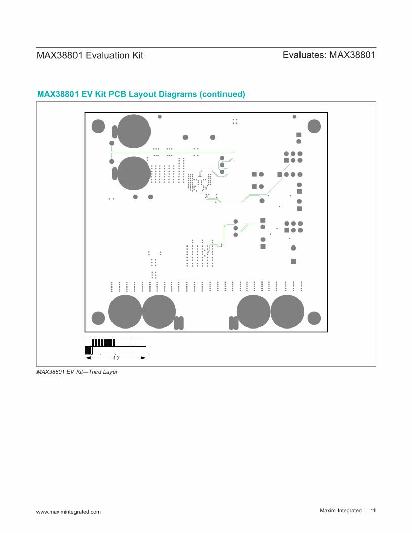
MAX38801 EV Kit—Third Layer
MAX38801 EV Kit PCB Layout Diagrams (continued)
1.0’’

Maxim Integrated 12www.maximintegrated.com
Evaluates: MAX38801MAX38801 Evaluation Kit
MAX38801 EV Kit—Bottom View
MAX38801 EV Kit PCB Layout Diagrams (continued)
1.0’’

Maxim Integrated 13www.maximintegrated.com
Evaluates: MAX38801MAX38801 Evaluation Kit
MAX38801 EV Kit—Bottom Silkscreen
MAX38801 EV Kit PCB Layout Diagrams (continued)
1.0’’
Maxim Integrated 14www.maximintegrated.com
Evaluates: MAX38801MAX38801 Evaluation Kit
#Denotes an RoHS-compliant device
PART TYPE
MAX38801EVKIT# EV Kit
Ordering Information

Maxim Integrated cannot assume responsibility for use of any circuitry other than circuitry entirely embodied in a Maxim Integrated product. No circuit patent licenses are implied. Maxim Integrated reserves the right to change the circuitry and specifications without notice at any time.
Maxim Integrated and the Maxim Integrated logo are trademarks of Maxim Integrated Products, Inc. © 2017 Maxim Integrated Products, Inc. 15
Evaluates: MAX38801MAX38801 Evaluation Kit
REVISIONNUMBER
REVISIONDATE DESCRIPTION PAGES
CHANGED
0 8/17 Initial release —
Revision History
For pricing, delivery, and ordering information, please contact Maxim Direct at 1-888-629-4642, or visit Maxim Integrated’s website at www.maximintegrated.com.