max5988a evaluation kit evaluates: max5988a - maxim … · vss, vss1 2 black test points — 1 pcb:...
TRANSCRIPT
General DescriptionThe MAX5988A evaluation kit (EV kit) is a fully assembled and tested surface-mount circuit board featuring an Ethernet port, network powered-device (PD) interface controller circuit for -57V supply rail systems. The EV kit uses the MAX5988A IEEE® 802.3af/at-compliant network PD interface controller in a 20-pin TQFN package with an exposed pad. The IC is used in Power-over-LAN (PoL) applications requiring DC power from an Ethernet network port for PDs such as IP phones, wireless access nodes, and security cameras.The EV kit receives power from IEEE 802.3af/at- compliant power-sourcing equipment (PSE). Refer to the MAX5988A IC data sheet for PSE controllers. The PSE provides the required -36V to -57V DC power over an unshielded twisted-pair Ethernet network cable to the EV kit’s RJ45 magnetic jack. The EV kit features a 1 x 1 gigabit RJ45 magnetic jack and two active full-wave rectifiers (DM1, DM2) for separating the DC power provided by an endspan or midspan Ethernet system.The EV kit can also be powered by a wall adapter power source. The EV kit provides PCB pads to accept the out-put of a wall adapter power source. When a wall adapter power source is detected, it always takes precedence over the PSE source and allows the wall adapter to power the EV kit.The EV kit demonstrates the full functionality of the IC, such as PD detection signature, PD classification signa-ture, inrush current control, input undervoltage lockout (UVLO), and an integrated DC-DC step-down converter. The integrated step-down converter operates at a fixed 215kHz switching frequency and is configured for a non-isolated +5V DC output that can deliver 1.5A of current.Warning: The EV kit is designed to operate with high volt-ages. Dangerous voltages are present on this EV kit and on equipment connected to it. Users who power up this EV kit or power the sources connected to it must be careful to follow safety procedures appropriately to work with high-voltage electrical equipment.Under severe fault or failure conditions, this EV kit may dissipate large amounts of power, which could result in the mechanical ejection of a component or of component debris at high velocity. Operate this kit with care to avoid possible personal injury.
Features IEEE802.3af/at-CompliantPDInterfaceCircuit PoEClass1/Class2 -36Vto-57VInputRange DemonstratesanIntegrated6.49WStep-Down
DC-DC Converter +5VOutputat1.15A InrushCurrentLimitof49mA(typ) EvaluatesEndspanandMidspanEthernetSystems SimplifiedWallAdapterInterface ProvenPCBLayout FullyAssembledandTested
19-8555; Rev 0; 8/16
Ordering Information appears at end of data sheet.
DESIGNATION QTY DESCRIPTION
C1, C2 20.1µF ±10%, 100V X7R ceramic capacitors (0603)Murata GRM188R72A104K
C3, C4 20.1µF ±10%, 50V X7R ceramic capacitors (0603)Murata GRM188R71H104K
C5, C8, C9 31µF ±10%, 25V X7R ceramic capacitors (0603)Murata GRM188R71E105K
C6, C7 21µF ±10%, 100V X7R ceramic capacitors (1206)Murata GRM31CR72A105K
C10 1
10µF ±20%, 80V aluminum electrolytic capacitor (6.3mm X 7.7mm)Panasonic EEE-FK1K100XP
C11 0 Not installed, ceramic capacitor (0402)
C12 1100µF ±10%, 6.3V X5R ceramic capacitor (1206)Murata GRM31CR60J107ME39L
MAX5988A Evaluation Kit Evaluates: MAX5988A
Component List
Note: Indicate that you are using the MAX5988A when contacting these component suppliers.
DESIGNATION QTY DESCRIPTION
C13, C14 0 Not installed, ceramic capacitors (1206)
D1, D2 2 LEDs (SMB)Kingbright AA3528ACGCK
D3–D8 6 100V, 2A Schottky diodes (SMB)Diodes Inc. B2100
D9 0 Not installed, zener diode (SOD323)
D10–D13 4 12V, 200mW zener diodes (SOD323)Diodes Inc. BZT52C12S-7-F
DM1, DM2 2100V, 3.5A dual n-channel MOSFETs (8 SO)Fairchild FDS86141
J1 1RJ45 MagJack 1G Ethernet, 802.3af/at standardBel Fuse Inc. 0826-1X1T-AC-F
JU1 1 2-pin header
L1 147µH, 2.5A inductor (12.4mm x 12.4mm)Sumida CDRH127NP-470MC
LDO_OUT, SLEEP, ULP 3 Orange miniature test points
Q1, Q2 2 Signal n-channel MOSFETs (SOT 23)Fairchild 2N7002
R1 1 100kΩ±1%resistor(0402)R2–R6 5 49.9kΩ±1%resistors(0402)
DESIGNATION QTY DESCRIPTIONR7–R9,
R12–R14 6 0Ω±1%resistors(0603)
R10, R11 0 Not installed, resistors (0603)R15–R18 4 499kΩ±1%resistors(0402)R19–R21 3 24.9kΩ±1%resistors(0402)
R22 1 1kΩ±1%resistor(0603)R23, R25, R28 0 Not installed, resistors (0402)
R24 1 0Ω±1%resistor(0402)R26 1 2.49kΩ±1%resistor(0402)R27 1 7.5kΩ±1%resistor(0402)
R29, R30 2 10kΩ±1%resistors(0402)R31 1 60.4kΩ±1%resistor(0603)
SW1 0
Not installed, 6mm tact 160GF switch (H = 4.3MM)Omron Electronics Inc. ECB Div: B3S-1000P
U1 1PD with integrated DC-DC converter (20 TQFN-EP*)Maxim MAX5988A
VDD1, VOUT1 2 Red test pointsVSS 1 Green miniature test point
VSS, VSS1 2 Black test points— 1 PCB: MAX5988A EVALUATION KIT
SUPPLIER PHONE WEBSITEBel Fuse Inc. 201-432-0463 www.belfuse.comDiodes Incorporated 805-446-4800 www.diodes.comFairchild Semiconductor 888-522-5372 www.fairchildsemi.comKingbright Corporation 909-468-0500 www.kingbrightusa.comMurata Electronics North America, Inc. 770-436-1300 www.murata-northamerica.comPanasonic Corp. 800-344-2112 www.panasonic.comSumida Corp. 847-545-6700 www.sumida.com
Maxim Integrated 2
MAX5988A Evaluation Kit Evaluates: MAX5988A
www.maximintegrated.com
Component Suppliers
Component List (continued)
*EP = Exposed pad.
Quick StartRequired Equipment MAX5988AEVkit IEEE 802.3af/at-compliant PSE and a Category 5e
Ethernet network cable -48V,1AcapableDCpowersupply Voltmeter
Hardware ConnectionsThe EV kit is fully assembled and tested. Follow the steps below to verify board operation. Caution: Do not turn on the power supply until all connections are completed.1) Use one of the following methods to power the EV kit: a. If network connectivity is required: Connect a
Category 5e Ethernet network cable from the EV kit input port RJ45 connector to the corresponding PSE Ethernet LAN connection that provides power to the EV kit.
b. If network connectivity is not required: Connect a -48V DC power supply between the VSS and VDD1 PCB pads on the EV kit. Connect the power-supply positive terminal to the VDD1 PCB pad and the negative terminal to the VSS PCB pad.
2) Activate the PSE power supply or turn on the external DC power supply.
3) Using a voltmeter, verify that the EV kit provides +5V across the VOUT1 and VSS PCB pads.
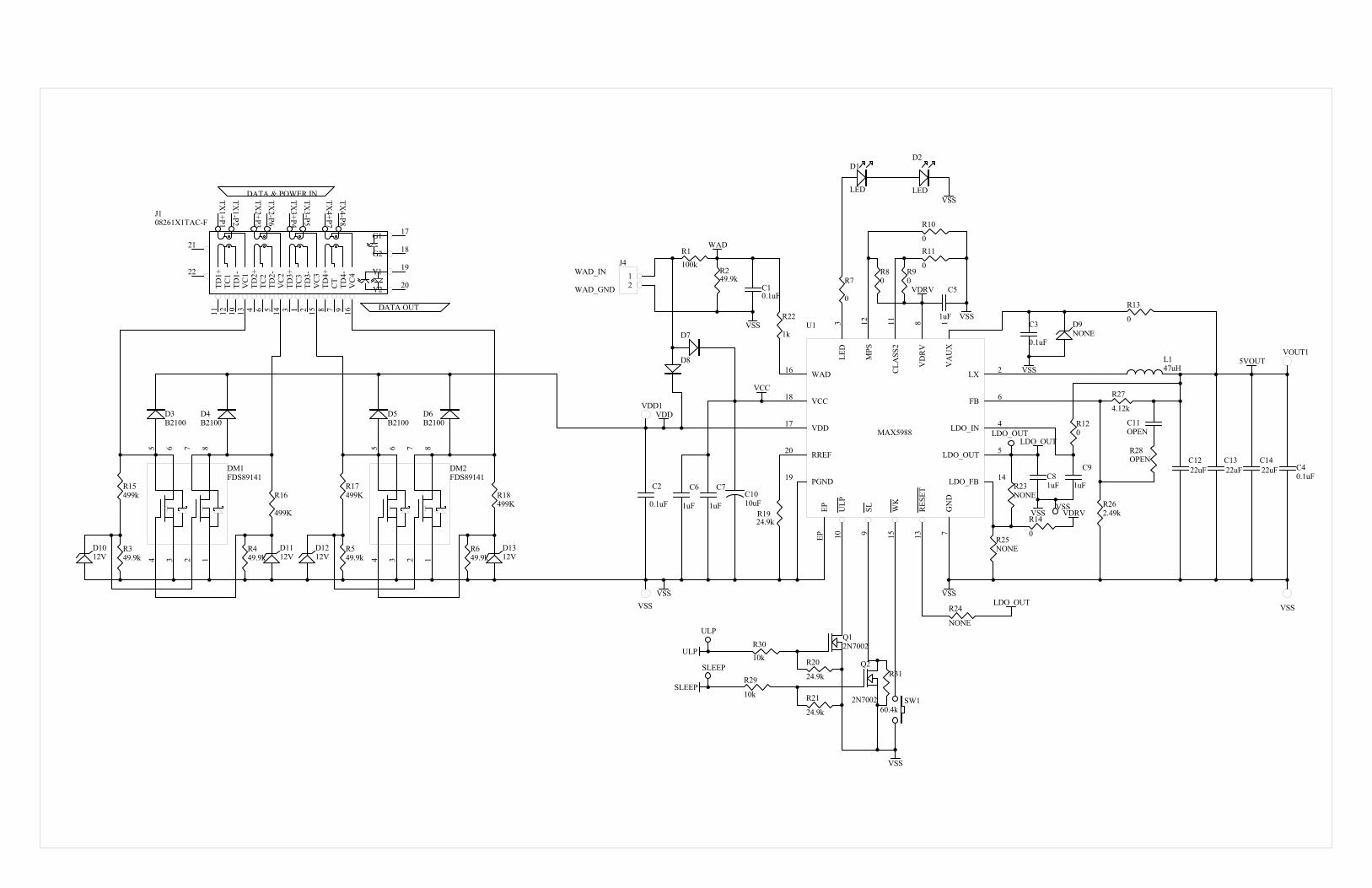
Detailed Description of HardwareThe MAX5988A EV kit features an Ethernet port and network PD interface controller circuit for -57V supply rail systems. The EV kit contains a MAX5988A IEEE 802.3af/at-compliant network PD interface controller in a 20-pin TQFN-EP package. The IC is used in PoL applications for powering PDs from an unshielded twisted-pair (UTP) Ethernet Category 5e network cable and PSE port using endspan or midspan Ethernet systems.The EV kit receives power from an IEEE 802.3af/at-compliant PSE and a UTP cable connected to the EV kit’s RJ45 magnetic jack. The EV kit uses a 1 x 1 gigabit RJ45 magnetic jack and two active full-wave bridge power rectifiers to separate the -57V DC power sent by the PSE. The EV kit can accept power from an endspan or midspan PSE network configuration.The EV kit can also accept power from a wall adapter power source. When a wall adapter power source is
detected between the WAD_IN and WAD_GND PCB pads, the IC’s internal isolation switch disconnects VCC from VDD, which allows the wall adapter to supply power to the EV kit.The EV kit demonstrates the full functionality of the IC such as PD detection signature, PD classification signature, inrush current control, and UVLO. Setting the EV kit as Class 2 PD is done by installing resistors R9 and opening R11. Do not install R9 and R11 at the same time.The EV kit’s integrated DC-DC step-down converter is configured for a nonisolated output voltage of +5V and provides up to 1.2A at the output while achieving up to 87.3% and 92.2% efficiencies at the +36V and +12V input, respectively. The integrated step-down converter operates at a fixed 215kHz switching frequency.
Maintain Power Signature (MPS)The MPS frunction is enabled by connect-ing the MPS pin to VDRV. This is done by installing resistors R8 and opening R10. Do not install R8 and R10 at the same time.
Wall Adapter Power Source (WAD_IN, WAD_GND)The EV kit can also accept power from a wall adapter power source. Use the WAD_IN (0V) and WAD_GND (-10V to -57V) PCB pads to connect the wall adapter power source. The wall adapter power source operating-voltage range must be within +10V to +57V for the EV kit.When the wall adapter power source is above +10V it always takes precedence over the PSE source. Once the wall adapter power source is detected, the IC’s internal isolation switch disconnects VCC from VDD. The wall adapter power is supplied to VCC (through diode D7) and VSS. Once it takes over, the classification process is disabled.When the wall adapter power source is below +8.5V, the PSE provides power through the IC’s VSS. Diode D2 pre-vents the PSE from back-driving the wall adapter power source when it is below +8.5V.
Undervoltage Lockout (UVLO)The EV kit operates up to a -57V supply with a turn-on UVLO threshold (VON) at -40V and a turn-off UVLO threshold (VOFF) at -30V. When the input voltage is above VON, the EV kit is enabled. When the input voltage goes below VOFF, the EV kit is disabled.
Maxim Integrated 3
MAX5988A Evaluation Kit Evaluates: MAX5988A
www.maximintegrated.com
#Denotes RoHS compliant.
PART TYPEMAX5988AEVKIT# EV Kit
Maxim Integrated 4
MAX5988A Evaluation Kit Evaluates: MAX5988A
www.maximintegrated.com
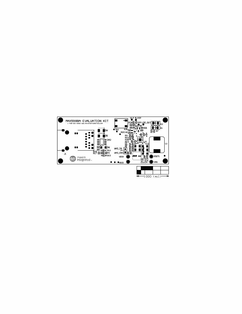
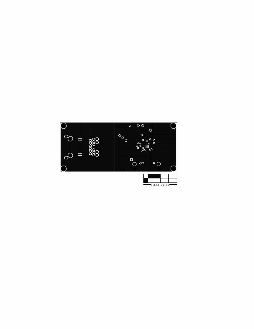
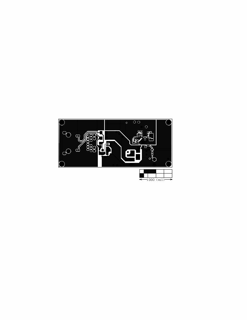
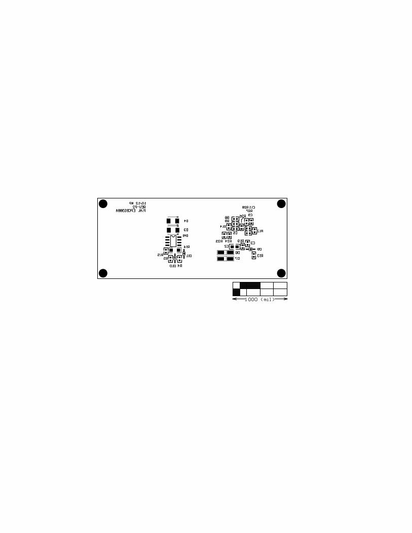
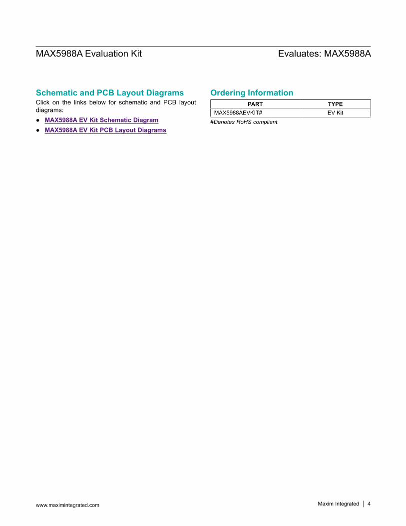
Schematic and PCB Layout DiagramsClick on the links below for schematic and PCB layout diagrams: MAX5988A EV Kit Schematic Diagram MAX5988A EV Kit PCB Layout Diagrams
Ordering Information
REVISIONNUMBER
REVISIONDATE DESCRIPTION PAGES
CHANGED0 8/16 Initial release —
Maxim Integrated cannot assume responsibility for use of any circuitry other than circuitry entirely embodied in a Maxim Integrated product. No circuit patent licenses are implied. Maxim Integrated reserves the right to change the circuitry and specifications without notice at any time.
MAX5988A Evaluation Kit Evaluates: MAX5988A
Maxim Integrated and the Maxim Integrated logo are trademarks of Maxim Integrated Products, Inc. © 2016 Maxim Integrated Products, Inc. 5
Revision History
For pricing, delivery, and ordering information, please contact Maxim Direct at 1-888-629-4642, or visit Maxim Integrated’s website at www.maximintegrated.com.
C2
0.1uFR1924.9k
C10.1uF
R262.49k
12
J4
VCC
VSS
WAD
R27
4.12k
VSS
D7
5VOUT
R1
100kR249.9k
VSS
VSS
VDD1
VSS
VDD
C1322uF
L147uH
C5
1uFC3
0.1uF
D2
LED
D1
LED
Q12N7002
Q2
2N7002
VSS
ULP
SLEEP
C40.1uF
R30
10k R20
24.9kR29
10k R21
24.9k
ULP
SLEEP
VOUT1
R7
0
C11OPEN
R28OPEN
R13
0
C1422uF
R22
1k
C7
1uF
D9NONE
R11
0
R10
0
R23NONE
R120
R25NONE
R14
0
VDRV
VDRV
LDO_OUT
C9
1uFC81uF
VSS
R24
NONE
LDO_OUT
LDO_OUT
D8
R31
60.4k
VSS
R15499k
R349.9k
R16
499K
R449.9k
D3B2100
12345 6 7
8
DM1FDS89141
R17499K
R549.9k
R649.9k
D5B2100
12345 6 7
8
DM2FDS89141
D1012V
D1112V
D1212V
D1312V
D4B2100
D6B2100
TC1
12
TD1-
10
TD1+
11
TX1+P1
TX1-P2
Y2 20
G2 18
Y1 19
G1 17
21
22
VC
113
TC2
6
TD2-
5
TD2+
4
TX2+P3
TX2-P6
VC
214
TC3
1
TD3-
2
TD3+
3
TX3+P4
TX3-P5
VC
315
CT
7
TD4-
9
TD4+
8
TX4+P7
TX4-P8
VC
416
J108261X1TAC-F
DATA & POWER IN
DATA OUTVSS
R90
R80
C1222uF
LX 2
LED
3
MPS
12
WK
15
FB 6
VD
RV
8
ULP
10
CLA
SS2
11
RREF20
WAD16
EPEP
VA
UX
1
PGND19
VCC18
VDD17
GN
D7
SL9
LDO_FB 14
LDO_OUT 5
LDO_IN 4
RES
ET13
U1
MAX5988
C1010uF
R18499K
SW1
C6
1uF
VSS VSS
WAD_GND
WAD_IN