max77650/max77651 programmer’s guide - maxim … · max77650/max77651 programmer’s guide...
TRANSCRIPT

MAX77650/MAX77651 Programmer’s Guide
UG6428; Rev 0; 5/17
Abstract The MAX77650/MAX77651 provide highly integrated battery charging and power supply solutions for low-power
applications where size and efficiency are critical. The MAX77650/MAX77651 device datasheet provides the
complete hardware and electrical description for these devices. This Programmer’s Guide focuses on the
register map for the devices and provides general advice for programmers.

Maxim Integrated Page 1 of 53
Contents 1 OTP Options ............................................................................................................................................ 3
2 OTP Registers Quick Reference Table ................................................................................................... 3
3 Register Reset Conditions ....................................................................................................................... 4
3.1 System Power-On Reset Comparator (POR) .......................................................................................... 4
3.2 System Reset (SYSRST)......................................................................................................................... 4
3.3 CHGPOK ................................................................................................................................................. 4
3.4 CHGPOR ................................................................................................................................................. 4
4 Baseline Initialization ............................................................................................................................... 5
5 Software Management of the Charger .................................................................................................... 6
5.1 Managing VSYS_REG, CHG_CV, and CHG_CV_JEITA ....................................................................... 6
6 Managing SIMO Current Limits (IP_SBBx) ............................................................................................. 7
7 Managing Main-Bias Circuits (SBIA_LPM) .............................................................................................. 7
8 Changing Regulator Output Voltages ...................................................................................................... 8
9 Register Description ................................................................................................................................ 9
9.1 Register Descriptions: Global Resources ............................................................................................... 9
9.1.1 CNFG_GLBL ........................................................................................................................ 9 9.1.2 INT_GLBL .......................................................................................................................... 10 9.1.3 INTM_GLBL ....................................................................................................................... 11 9.1.4 STAT_GLBL ....................................................................................................................... 12 9.1.5 ERCFLAG .......................................................................................................................... 13 9.1.6 CNFG_GPIO ...................................................................................................................... 14 9.1.7 CID ..................................................................................................................................... 15
9.2 Register Descriptions: Charger ............................................................................................................ 16
9.2.1 INT_CHG ........................................................................................................................... 16 9.2.2 INT_M_CHG ...................................................................................................................... 17 9.2.3 STAT_CHG_A ................................................................................................................... 18 9.2.4 STAT_CHG_B ................................................................................................................... 19 9.2.5 CNFG_CHG_A .................................................................................................................. 20 9.2.6 CNFG_CHG_B .................................................................................................................. 21 9.2.7 CNFG_CHG_C .................................................................................................................. 22 9.2.8 CNFG_CHG_D .................................................................................................................. 23 9.2.9 VSYS_REG Code Table .................................................................................................... 23 9.2.10 CNFG_CHG_E .................................................................................................................. 24 9.2.11 CHG_CC and CHG_CC_JEITA Code Table ..................................................................... 25 9.2.12 CNFG_CHG_F ................................................................................................................... 26 9.2.13 CNFG_CHG_G .................................................................................................................. 27 9.2.14 CHG_CV and CHG_CV_JEITA Code Table ..................................................................... 28 9.2.15 CNFG_CHG_H .................................................................................................................. 29 9.2.16 CNFG_CHG_I .................................................................................................................... 30 9.2.17 IMON_DISCHG_SCALE Code Table ................................................................................ 30
9.3 Register Descriptions: LDO .................................................................................................................. 31
9.3.1 CNFG_LDO_A ................................................................................................................... 31 9.3.2 TV_LDO Code Table ......................................................................................................... 32 9.3.3 CNFG_LDO_B ................................................................................................................... 33
9.4 Register Descriptions: SIMO Buck Boost ............................................................................................. 34
9.4.1 CNFG_SBB_TOP .............................................................................................................. 34 9.4.2 CNFG_SBB0_A ................................................................................................................. 36 9.4.3 TV_SBB0 Code Table ........................................................................................................ 36 9.4.4 CNFG_SBB0_B ................................................................................................................. 37

Maxim Integrated Page 2 of 53
9.4.5 CNFG_SBB1_A ................................................................................................................. 38 9.4.6 MAX77650 TV_SBB1 Code Table ..................................................................................... 39 9.4.7 MAX77651 TV_SBB1 Code Table ..................................................................................... 40 9.4.8 CNFG_SBB1_B ................................................................................................................. 41 9.4.9 CNFG_SBB2_A ................................................................................................................. 42 9.4.10 MAX77650 TV_SBB2 Code Table ..................................................................................... 43 9.4.11 MAX77651 TV_SBB2 Code Table ..................................................................................... 43 9.4.12 CNFG_SBB2_B ................................................................................................................. 44
9.5 Register Descriptions: Current Sinks .................................................................................................... 45
9.5.1 CNFG_LED0_A ................................................................................................................. 45 9.5.2 CNFG_LED0_B ................................................................................................................. 46 9.5.3 CNFG_LED1_A ................................................................................................................. 47 9.5.4 CNFG_LED1_B ................................................................................................................. 48 9.5.5 CNFG_LED2_A ................................................................................................................. 49 9.5.6 CNFG_LED2_B ................................................................................................................. 50 9.5.7 CNFG_LED_TOP .............................................................................................................. 51 9.5.8 BRT_LEDx Code table when LED_FSx = 0b01 ................................................................ 52 9.5.9 BRT_LEDx Code table when LED_FSx = 0b10 ................................................................ 52 9.5.10 BRT_LEDx Code table when LED_FSx = 0b11 ................................................................ 53
10 Revision History ..................................................................................................................................... 53
Maxim Integrated Page 3 of 53
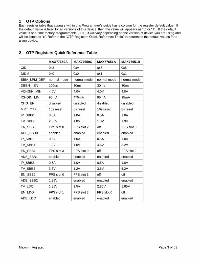
1 OTP Options Each register table that appears within this Programmer’s guide has a column for the register default value. If the default value is fixed for all versions of this device, then the value will appears as “0” or “1”. If the default value is one-time factory programmable (OTP) it will vary depending on the version of device you are using and will be listed as “x”. Refer to the “OTP Registers Quick Reference Table” to determine the default values for a given device.
2 OTP Registers Quick Reference Table
MAX77650A MAX77650C MAX77651A MAX77651B
CID 0x3 0xA 0x6 0x8
DIDM 0x0 0x0 0x1 0x1
SBIA_LPM_DEF normal mode normal mode normal mode normal mode
DBEN_nEN 100us 30ms 30ms 30ms
VCHGIN_MIN 4.0V 4.0V 4.0V 4.0V
ICHGIN_LIM 95mA 475mA 95mA 95mA
CHG_EN disabled disabled disabled disabled
MRT_OTP 16s reset 8s reset 16s reset 8s reset
IP_SBB0 0.5A 1.0A 0.5A 1.0A
TV_SBB0 2.05V 1.8V 1.8V 1.9V
EN_SBB0 FPS slot 0 FPS slot 2 off FPS slot 0
ADE_SBB0 enabled enabled enabled enabled
IP_SBB1 0.5A 1.0A 0.5A 1.0A
TV_SBB1 1.2V 1.0V 4.6V 3.2V
EN_SBB1 FPS slot 3 FPS slot 0 off FPS slot 2
ADE_SBB1 enabled enabled enabled enabled
IP_SBB2 0.5A 1.0A 0.5A 1.0A
TV_SBB2 3.3V 1.2V 3.6V 5.2V
EN_SBB2 FPS slot 0 FPS slot 1 off off
ADE_SBB2 1.85V enabled enabled enabled
TV_LDO 1.85V 1.5V 2.85V 1.85V
EN_LDO FPS slot 1 FPS slot 3 FPS slot 0 off
ADE_LDO enabled enabled enabled enabled

Maxim Integrated Page 4 of 53
3 Register Reset Conditions
3.1 System Power-On Reset Comparator (POR) The SYS POR comparator monitors VSYS and generates a power-on reset signal (POR). When VSYS is below VPOR, the device is held in reset (SYSRST=1). When VSYS rises above VPOR, internal signals and on-chip memory stabilize and the device is released from reset (SYSRST=0).
3.2 System Reset (SYSRST) The majority of the registers within the device have the reset condition of SYSRST=1. The SYSRST signal is created by the “On/Off Controller” logic and is continuously high when the system voltage is lower than the power-on reset threshold (VSYS<VPOR). Additionally, SYSRST is pulsed high to reset the registers during the on/off controller’s “immediate shutdown” routine and “power-down sequence” routine (See the datasheet’s On/Off Controller section for more information).
3.3 CHGPOK Registers with reset conditions specified as CHGPOK are held in their reset state whenever VCHGIN<VCHGIN_UVLO or USBS=1. These registers contain charger status information and the charger input current limit setting. Writes to these register while they are being held in reset are ignored.
3.4 CHGPOR The USBS bitfield is held in its reset state whenever VCHGIN < 1.8V. Writes to USBS while it is held in reset are ignored.
Maxim Integrated Page 5 of 53
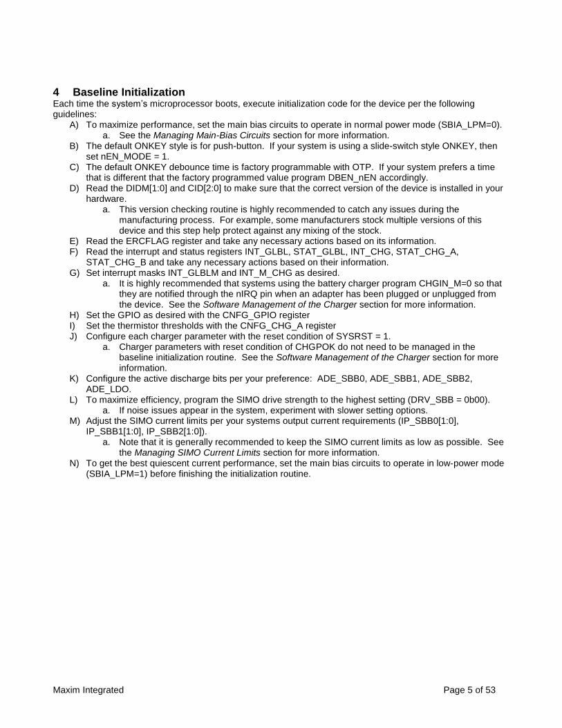
4 Baseline Initialization Each time the system’s microprocessor boots, execute initialization code for the device per the following guidelines:
A) To maximize performance, set the main bias circuits to operate in normal power mode (SBIA_LPM=0). a. See the Managing Main-Bias Circuits section for more information.
B) The default ONKEY style is for push-button. If your system is using a slide-switch style ONKEY, then set nEN_MODE = 1.
C) The default ONKEY debounce time is factory programmable with OTP. If your system prefers a time that is different that the factory programmed value program DBEN_nEN accordingly.
D) Read the DIDM[1:0] and CID[2:0] to make sure that the correct version of the device is installed in your hardware.
a. This version checking routine is highly recommended to catch any issues during the manufacturing process. For example, some manufacturers stock multiple versions of this device and this step help protect against any mixing of the stock.
E) Read the ERCFLAG register and take any necessary actions based on its information. F) Read the interrupt and status registers INT_GLBL, STAT_GLBL, INT_CHG, STAT_CHG_A,
STAT_CHG_B and take any necessary actions based on their information. G) Set interrupt masks INT_GLBLM and INT_M_CHG as desired.
a. It is highly recommended that systems using the battery charger program CHGIN_M=0 so that they are notified through the nIRQ pin when an adapter has been plugged or unplugged from the device. See the Software Management of the Charger section for more information.
H) Set the GPIO as desired with the CNFG_GPIO register I) Set the thermistor thresholds with the CNFG_CHG_A register J) Configure each charger parameter with the reset condition of SYSRST = 1.
a. Charger parameters with reset condition of CHGPOK do not need to be managed in the baseline initialization routine. See the Software Management of the Charger section for more information.
K) Configure the active discharge bits per your preference: ADE_SBB0, ADE_SBB1, ADE_SBB2, ADE_LDO.
L) To maximize efficiency, program the SIMO drive strength to the highest setting (DRV_SBB = 0b00). a. If noise issues appear in the system, experiment with slower setting options.
M) Adjust the SIMO current limits per your systems output current requirements (IP_SBB0[1:0], IP_SBB1[1:0], IP_SBB2[1:0]).
a. Note that it is generally recommended to keep the SIMO current limits as low as possible. See the Managing SIMO Current Limits section for more information.
N) To get the best quiescent current performance, set the main bias circuits to operate in low-power mode (SBIA_LPM=1) before finishing the initialization routine.

Maxim Integrated Page 6 of 53
5 Software Management of the Charger 1. All of the charger configuration except for the charger input current limit (ICHGIN_LIM) should be
managed in the baseline initialization routine. See the Baseline Initialization section for more information.
a. It is a common misperception that the fast charge current limit should be modulated based off the available capacity of the charge adapter and/or the system load current requirements. This is not correct. The fast charge current limit should be set based on the characteristics of the battery only. The charger automatically modulates the charge current as required to meet the input current limit or provide for system load current.
2. Charging only happens when the On/Off Controller is in the “On via On/Off Controller” state. 3. Although the charger configuration happens during the baseline initialization, it is recommended that the
processor read the charge configuration information periodically during the charge cycle as a safety measure to ensure everything is as it should be. It is critical that the battery regulation voltage (CHG_CV[5:0]) be correct.
4. Within the Baseline Initialization routine, program the charger interrupt mask (CHGIN_M) to 0. This allows any change in the charger input (CHGIN) status to be directly reported to the processor via the interrupt pin (nIRQ). See the Baseline Initialization section for more information.
5. When the charger input interrupt is pending (CHGIN_I=1), read the CHG_DTLS: a. when the charger input is okay (CHGIN_DTLS=0b11):
i. enumerate the charger input if it is a USB source (not through the MAX77650/51) ii. program the desired charger input current limit (ICHGIN_LIM[2:0]) iii. Read the charge configuration information to ensure it matches the desired values
programmed by the baseline initialization routine. This step is not necessary but it is a recommended safety measure.
iv. enable the charger (CHG_EN=1) b. when the charger input is in undervoltage lockout (CHGIN_DTLS=0b00):
i. disable the charger (CHG_EN=0) ii. note that the charger input current limit (ICHGIN_LIM) is continuously held in reset
during this condition c. when the charger input is in overvoltage lockout (CHGIN_DTLS=0b01):
i. disable the charger (CHG_EN=0) 1. this isn’t really necessary but recommended
ii. based on the user experience desired, software can either do nothing or provide a message to the user that something is wrong with their charge adapter and they should remove it from the device
d. when the charger input is being debounce (CHGIN_DTLS=0b10) i. based on the user experience desired, software can either do nothing or provide a
message to the user that the charger input has been applied to the system 1. Note that the charger input debounce time (tCHGIN-DB) is typically 120ms.
5.1 Managing VSYS_REG, CHG_CV, and CHG_CV_JEITA
Program VSYS_REG to at least 200mV above the higher of CHG_CV and CHG_CV_JEITA. Any write request that violates this requirement will cause the device to force CHG_CV and CHG_CV_JEITA to conform to this restraint. Example 1: Program CHG_CV to any value above (VSYS_REG – 200mV)
If a write command tries to program CHG_CV to any value above (VSYS_REG – 200mV), the device overrides the write and programs CHG_CV to (VSYS_REG – 200mV). For example, VSYS_REG = 4.5V and CHG_CV = 3.6V. A command tries to write CHG_CV to 4.4V; the device will override this and programs CHG_CV to 4.3V. Example 2: Program VSYS_REG below (CHG_CV + 200mV)

Maxim Integrated Page 7 of 53
If a write command tries to program VSYS_REG below (CHG_CV + 200mV), the device writes VSYS_REG to the requested voltage, but forces CHG_CV to (VSYS_REG – 200mV). For example, VSYS_REG = 4.5V and CHG_CV = 4.2V. A command programs VSYS_REG to 4.1V; the device will automatically program CHG_CV to 3.9V. Example 3: Programming VSYS_REG, CHG_CV, CHG_CV_JEITA Use Case
Take the following case: existing settings: VSYS_REG = 4.2V, CHG_CV =3.6V, CHG_CV_JEITA =3.6V desired settings: VSYS_REG = 4.4V, CHG_CV =4.2V, CHG_CV_JEITA =4.1V Incorrect Method:
1) program CHG_CV=4.2V 2) program CHG_CV_JEITA=4.1V 3) program VSYS_REG=4.4V
resulting settings are wrong: VSYS_REG = 4.4V, CHG_CV =4.0V, CHG_CV_JEITA =4.0V
Correct Method:
1) program VSYS_REG=4.4V 2) program CHG_CV=4.2V 3) program CHG_CV_JEITA=4.1V
resulting settings are correct: VSYS_REG = 4.4V, CHG_CV =4.2V, CHG_CV_JEITA =4.1V
6 Managing SIMO Current Limits (IP_SBBx) The available output current on a given SIMO channel is a function of the input voltage, the output voltage, the peak current limit setting, and the output current of the other SIMO channels. Maxim offers a SIMO calculator that outlines the available capacity for specific conditions. Generally speaking, applications should use the lowest possible SIMO peak current limit for a given mode of operation. Lower SIMO peak current settings give better efficiency, lower output voltage ripple, and lower noise. For example, if a system has increasing power states of OFF>>HIBERNATE>>STANDBY>> ACTIVE, then it is recommended to tailor the SIMO current limits for the power needs of each particular state. HIBERNATE may use 500mA for each SIMO channel, STANDBY may use 0.866A, 0.707A, and 0.5A for SIMO SBB0, SBB1, and SBB2, while ACTIVE may use 1A for each SIMO channel. Once again, see the SIMO calculator for guidance on how to size the current limits for a given set of power needs.
7 Managing Main-Bias Circuits (SBIA_LPM) 1) Applications that are not concerned about quiescent current may leave the main-bias circuits in their normal-
power mode indefinitely (SBIA_LPM=0) 2) Applications that are concerned about quiescent current and want to have a simple software structure may
leave the main-bias circuits in their low-power mode indefinitely (SBIA_LPM=1). 3) Applications that want to maximize performance and have low quiescent current should dynamically control
the main-bias circuits (SBIA_LPM). a) To maximize performance, set the main bias circuits to operate in normal power mode (SBIA_LPM=0)
whenever the system is doing a significant task. A tasks’ significance is judged according to how much quiescent current is consumed current is consumed by the system in order to accomplish that task relative to the quiescent current of the MAX77650/51 when it is in its low-power mode. Since the MAX77650/51 consumes ~5.6uA when all resources are enabled and its bias circuits in are low-power mode, then any task that is expected to consume more than ~2mA is significant.
b) To get the best quiescent current performance, set the main bias circuits to operate in low-power mode (SBIA_LPM=1) whenever the system’s current consumption is less than ~2mA.

Maxim Integrated Page 8 of 53
8 Changing Regulator Output Voltages The regulator output voltages are programmable. When a regulator is off, the output voltage may be directly programmed. However, when the regulator is on and the output voltage needs to be increased or decrease program a voltage ramp from the existing voltage to the new desired voltage. Programming a ramp is recommended for voltage increases to minimize inrush current. Programming a ramp is recommended on voltage decreases to minimize regulator undershoot when it reaches its target voltage. Example 4: Enabling a regulator to a static output voltage
1. When the regulator is disabled, program the output voltage to the desired value. 2. To maximize performance, set the main bias circuits to operate in normal-power mode. (SBIA_LPM=0),
wait 100us afterwards for the bias circuits to settle (not really needed but still a good idea). 3. Turn the regulator on. 4. To get the best quiescent current performance, wait for 2ms for the regulator to stabilize (enable delay +
soft-start ramp + margin), and then program the main bias circuits to operate in low-power mode (SBIA_LPM=1).
Example 5: ramping a regulator output voltage while it is enabled
1. To maximize performance, set the main bias circuits to operate in normal-power mode (SBIA_LPM=0), wait 100us afterwards for the bias circuits to settle (not really needed but still a good idea).
2. Ramp the regulator output voltage one LSB at a time (increasing or decreasing) until the target voltage is reached.
a. Note that for all regulators except the MAX77651 SBB1 the target voltage code tables are linear so, to step one LSB at a time, software can simply increment or decrement the bitfield value. However, for the MAX77651 SBB1, the code table is not linear and software should ensure that the output voltage is being stepped 50mV at a time. See section 10.4.7 MAX77651 TV_SBB1 Code Table for more information.
3. To get the best quiescent current performance, wait for 2ms for the regulator to stabilize (enable delay + soft-start ramp + margin), and then program the main bias circuits to operate in low-power mode (SBIA_LPM=1).

Maxim Integrated Page 9 of 53
9 Register Description The following tables detail the registers for the MAX77650/MAX77651. Undocumented register locations are reserved.
9.1 Register Descriptions: Global Resources
9.1.1 CNFG_GLBL
Register Name CNFG_GLBL
I2C Slave Address function of ADDR OTP bit
Register Address 0x10
Reset Value (HEX) OTP
Reset Value (BIN) 0b00x00x00
Reset Condition SYSRST=1
Access Type Mixed
Register Type Configuration
Bit Default Bit Name Description Reset Access Type
7 0 RESERVED Reserved. Unutilized bit. Write to 0. Reads are don't care. SYSRST=1 R/W
6 0 BOK Main Bias Okay Status Bit 0 = Main Bias not ready. 1 = Main Bias enabled and ready.
SYSRST=1 R
5 x SBIA_LPM Main Bias Low-Power Mode software request 0 = Main Bias requested to be in Normal Power Mode by software. 1 = Main Bias request to be in Low Power Mode by software.
SYSRST=1 R/W
4 0 SBIA_EN
Main Bias Enable Software Request 0 = Main Bias not enabled by software. Note that the main bias may be on via the on/off controller circuitry. 1 = Main Bias force enabled by software
SYSRST=1 R/W
3 0 nEN_MODE nEN Input (ONKEY) Default Configuration Mode 0 = Push-Button Mode 1 = Slide-Switch Mode
SYSRST=1 R/W
2 x DBEN_nEN Debounce Timer Enable for the nEN Pin 0 = 100us Debounce 1 = 30ms Debounce
SYSRST=1 R/W
1 0 SFT_RST[1:0]
Software Reset Functions. See the "On/Off Controller" section of the datasheet for more information. 0b00 = No Action 0b01 = Software Cold Reset (SFT_CRST). The device powers down, resets, and the powers up again. 0b10 = Software Off (SFT_OFF). The device powers down, resets, and then remains off and waiting for a wakeup event. 0b11 = Reserved Note that unlike most every other I2C write in this device that happens virtually immediately after the I2C acknowledge, the ST_CRST and SFT_OFF commands go through the power down sequence flow as described in the datasheet. This power down sequence flow has delay elements that add up to 205.24ms (60ms delay + 10.24ms nRST assert delay + 4x2.56ms power down slot delays + 125ms output discharge delay). If issuing the SFT_CRST and/or SFT_OFF functions in software, please wait for >300ms before trying to issue any additional commands via I2C.
SYSRST=1 R/W
0 0 SYSRST=1 R/W
Maxim Integrated Page 10 of 53
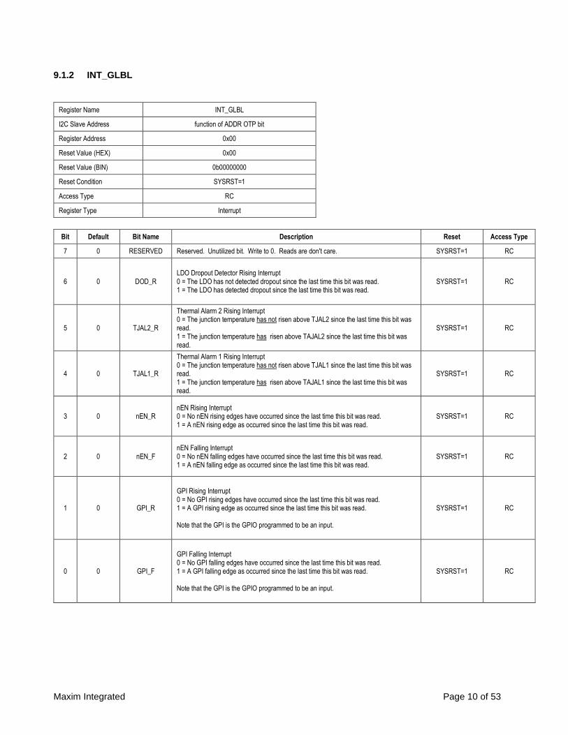
9.1.2 INT_GLBL
Register Name INT_GLBL
I2C Slave Address function of ADDR OTP bit
Register Address 0x00
Reset Value (HEX) 0x00
Reset Value (BIN) 0b00000000
Reset Condition SYSRST=1
Access Type RC
Register Type Interrupt
Bit Default Bit Name Description Reset Access Type
7 0 RESERVED Reserved. Unutilized bit. Write to 0. Reads are don't care. SYSRST=1 RC
6 0 DOD_R LDO Dropout Detector Rising Interrupt 0 = The LDO has not detected dropout since the last time this bit was read. 1 = The LDO has detected dropout since the last time this bit was read.
SYSRST=1 RC
5 0 TJAL2_R
Thermal Alarm 2 Rising Interrupt 0 = The junction temperature has not risen above TJAL2 since the last time this bit was read. 1 = The junction temperature has risen above TAJAL2 since the last time this bit was read.
SYSRST=1 RC
4 0 TJAL1_R
Thermal Alarm 1 Rising Interrupt 0 = The junction temperature has not risen above TJAL1 since the last time this bit was read. 1 = The junction temperature has risen above TAJAL1 since the last time this bit was read.
SYSRST=1 RC
3 0 nEN_R nEN Rising Interrupt 0 = No nEN rising edges have occurred since the last time this bit was read. 1 = A nEN rising edge as occurred since the last time this bit was read.
SYSRST=1 RC
2 0 nEN_F nEN Falling Interrupt 0 = No nEN falling edges have occurred since the last time this bit was read. 1 = A nEN falling edge as occurred since the last time this bit was read.
SYSRST=1 RC
1 0 GPI_R
GPI Rising Interrupt 0 = No GPI rising edges have occurred since the last time this bit was read. 1 = A GPI rising edge as occurred since the last time this bit was read. Note that the GPI is the GPIO programmed to be an input.
SYSRST=1 RC
0 0 GPI_F
GPI Falling Interrupt 0 = No GPI falling edges have occurred since the last time this bit was read. 1 = A GPI falling edge as occurred since the last time this bit was read. Note that the GPI is the GPIO programmed to be an input.
SYSRST=1 RC
Maxim Integrated Page 11 of 53
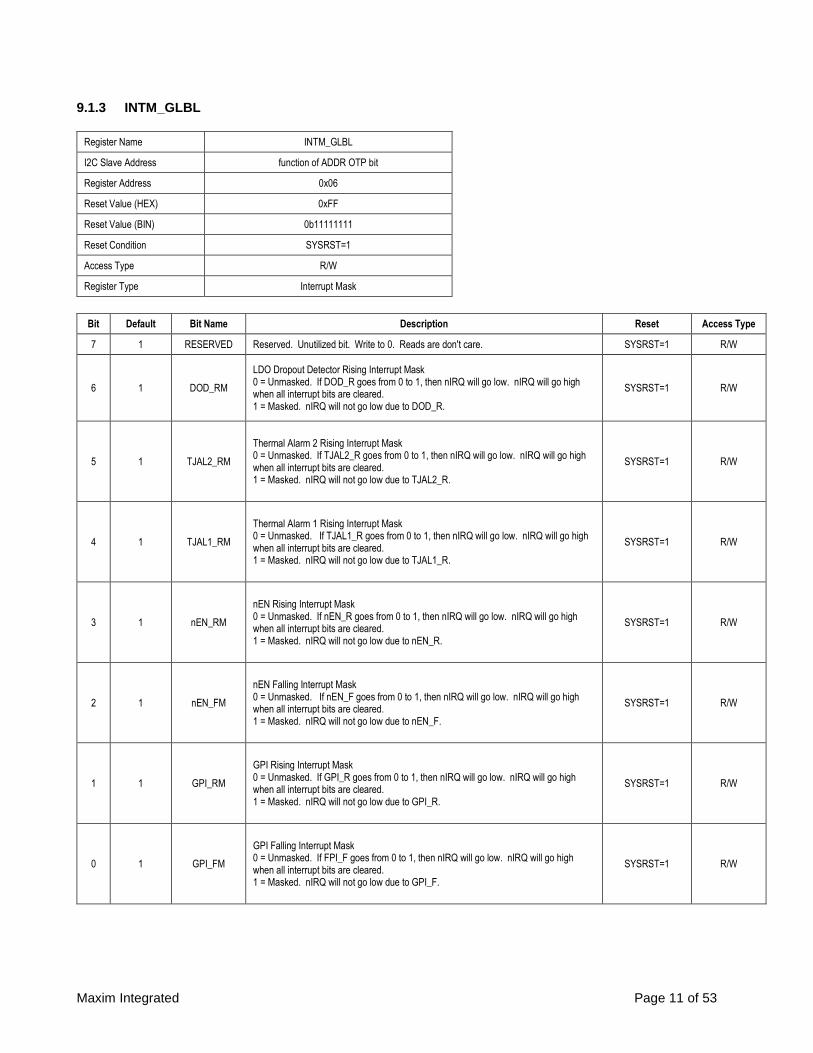
9.1.3 INTM_GLBL
Register Name INTM_GLBL
I2C Slave Address function of ADDR OTP bit
Register Address 0x06
Reset Value (HEX) 0xFF
Reset Value (BIN) 0b11111111
Reset Condition SYSRST=1
Access Type R/W
Register Type Interrupt Mask
Bit Default Bit Name Description Reset Access Type
7 1 RESERVED Reserved. Unutilized bit. Write to 0. Reads are don't care. SYSRST=1 R/W
6 1 DOD_RM
LDO Dropout Detector Rising Interrupt Mask 0 = Unmasked. If DOD_R goes from 0 to 1, then nIRQ will go low. nIRQ will go high when all interrupt bits are cleared. 1 = Masked. nIRQ will not go low due to DOD_R.
SYSRST=1 R/W
5 1 TJAL2_RM
Thermal Alarm 2 Rising Interrupt Mask 0 = Unmasked. If TJAL2_R goes from 0 to 1, then nIRQ will go low. nIRQ will go high when all interrupt bits are cleared. 1 = Masked. nIRQ will not go low due to TJAL2_R.
SYSRST=1 R/W
4 1 TJAL1_RM
Thermal Alarm 1 Rising Interrupt Mask 0 = Unmasked. If TJAL1_R goes from 0 to 1, then nIRQ will go low. nIRQ will go high when all interrupt bits are cleared. 1 = Masked. nIRQ will not go low due to TJAL1_R.
SYSRST=1 R/W
3 1 nEN_RM
nEN Rising Interrupt Mask 0 = Unmasked. If nEN_R goes from 0 to 1, then nIRQ will go low. nIRQ will go high when all interrupt bits are cleared. 1 = Masked. nIRQ will not go low due to nEN_R.
SYSRST=1 R/W
2 1 nEN_FM
nEN Falling Interrupt Mask 0 = Unmasked. If nEN_F goes from 0 to 1, then nIRQ will go low. nIRQ will go high when all interrupt bits are cleared. 1 = Masked. nIRQ will not go low due to nEN_F.
SYSRST=1 R/W
1 1 GPI_RM
GPI Rising Interrupt Mask 0 = Unmasked. If GPI_R goes from 0 to 1, then nIRQ will go low. nIRQ will go high when all interrupt bits are cleared. 1 = Masked. nIRQ will not go low due to GPI_R.
SYSRST=1 R/W
0 1 GPI_FM
GPI Falling Interrupt Mask 0 = Unmasked. If FPI_F goes from 0 to 1, then nIRQ will go low. nIRQ will go high when all interrupt bits are cleared. 1 = Masked. nIRQ will not go low due to GPI_F.
SYSRST=1 R/W
Maxim Integrated Page 12 of 53
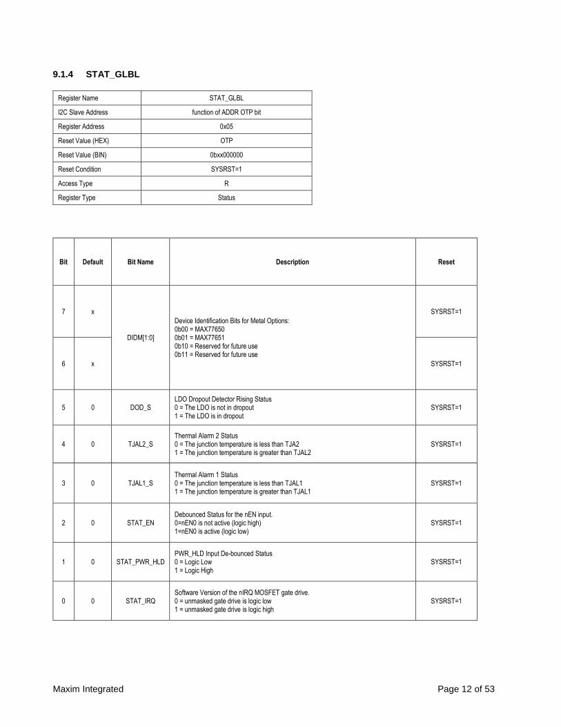
9.1.4 STAT_GLBL
Register Name STAT_GLBL
I2C Slave Address function of ADDR OTP bit
Register Address 0x05
Reset Value (HEX) OTP
Reset Value (BIN) 0bxx000000
Reset Condition SYSRST=1
Access Type R
Register Type Status
Bit Default Bit Name Description Reset
7 x
DIDM[1:0]
Device Identification Bits for Metal Options: 0b00 = MAX77650 0b01 = MAX77651 0b10 = Reserved for future use 0b11 = Reserved for future use
SYSRST=1
6 x SYSRST=1
5 0 DOD_S LDO Dropout Detector Rising Status 0 = The LDO is not in dropout 1 = The LDO is in dropout
SYSRST=1
4 0 TJAL2_S Thermal Alarm 2 Status 0 = The junction temperature is less than TJA2 1 = The junction temperature is greater than TJAL2
SYSRST=1
3 0 TJAL1_S Thermal Alarm 1 Status 0 = The junction temperature is less than TJAL1 1 = The junction temperature is greater than TJAL1
SYSRST=1
2 0 STAT_EN Debounced Status for the nEN input. 0=nEN0 is not active (logic high) 1=nEN0 is active (logic low)
SYSRST=1
1 0 STAT_PWR_HLD PWR_HLD Input De-bounced Status 0 = Logic Low 1 = Logic High
SYSRST=1
0 0 STAT_IRQ Software Version of the nIRQ MOSFET gate drive. 0 = unmasked gate drive is logic low 1 = unmasked gate drive is logic high
SYSRST=1

Maxim Integrated Page 13 of 53
9.1.5 ERCFLAG
Register Name ERCFLAG
I2C Slave Address function of ADDR OTP bit
Register Address 0x04
Reset Value (HEX) 0x00
Reset Value (BIN) 0b00000000
Reset Condition POR=1
Access Type RC
Register Type Status
Bit Default Bit Name Description Reset Access Type
7 0 RESERVED Reserved. Unutilized bit. Write to 0. Reads are don't care. POR=1 RC
6 0 PWR_HLD_RST
PWR_HLD Reset 0= A Reset has not occurred due to PWR_HLD2 deassertion since this last read of this register. 1= A Reset has occurred due to PWR_HLD2 deassertion since this last read of this register.
POR=1 RC
5 0 SFT_CRST_F
Software Cold Reset Flag 0 = The software cold reset has not occurred since the last read of this register. 1 = The software cold reset has occurred since the last read of this register. This indicates that software has set SFT_RST=0b01.
POR=1 RC
4 0 SFT_OFF_F
Software Off Flag 0 = The SFT_OFF function has not occurred since the last read of this register. 1 = The SFT_OFF function has occurred since the last read of this register. This indicates that software has set SFT_RST=0b10.
POR=1 RC
3 0 MRST Manual Reset Timer 0 = A Manual Reset has not occurred since this last read of this register. 1 = A Manual Reset has occurred since this last read of this register.
POR=1 RC
2 0 SYSUVLO
SYS Domain Undervoltage Lockout 0 = The SYS domain undervoltage lockout has not occurred since this last read of this register. 1 = The SYS domain undervoltage lockout has occurred since the last read of this register. This indicates that the SYS domain voltage fell below VSYSUVLO (~2.4V)
POR=1 RC
1 0 SYSOVLO
SYS Domain Overvoltage Lockout 0 = The SYS domain overvoltage lockout has not occurred since this last read of this register. 1 = The SYS domain overvoltage lockout has occurred since the last read of this register. This indicates that the SYS domain voltage rose below VSYSOVLO (~5.85V)
POR=1 RC
0 0 TOVLD
Thermal Overload 0 = The thermal overload has not occurred since the last read of this register. 1 = The thermal overload has occurred since the list read of this register. This indicates that the junction temperature has exceeded 165C.
POR=1 RC

Maxim Integrated Page 14 of 53
9.1.6 CNFG_GPIO
Register Name CNFG_GPIO
I2C Slave Address function of ADDR OTP bit
Register Address 0x12
Reset Value (HEX) 0x01
Reset Value (BIN) 0b00000001
Reset Condition SYSRST=1
Access Type Mixed
Register Type Mixed
Bit Default Bit Name Description Reset Access Type
7 0 RESERVED Reserved. Unutilized bit. Write to 0. Reads are don't care. SYSRST=1 R/W
6 0 RESERVED Reserved. Unutilized bit. Write to 0. Reads are don't care. SYSRST=1 R/W
5 0 RESERVED Reserved. Unutilized bit. Write to 0. Reads are don't care. SYSRST=1 R/W
4 0 DBEN_GPI General Purpose Input Debounce Timer Enable 0 = no debounce 1 = 30ms debounce
SYSRST=1 R/W
3 0 DO
General Purpose Output Data Output When set for GPO (DIR=0): 0 = GPIO is output is logic low 1 = GPIO is output logic high when set as push-pull output (DRV=1). GPIO is high-impedance when set as a and open-drain output (DRV=0).
When set for GPI (DIR=1): DO are don’t care when GPI.
SYSRST=1 R/W
2 0 DRV
General Purpose Output Driver Type When set for GPO (DIR=0): 0=open-drain 1=Push-Pull
When set for GPI (DIR=1): DRVx is a don’t care when GPI.
SYSRST=1 R/W
1 0 DI
GPIO Digital Input Value. Irrespective of whether the GPIO is set for GPI (DIR=1) or GPO (DIR=0), DI reflects the state of the GPIO. 0=input logic low 1=input logic high
SYSRST=1 R
0 1 DIR GPIO Direction. 0=General purpose output (GPO) 1=General purpose input (GPI)
SYSRST=1 R/W

Maxim Integrated Page 15 of 53
9.1.7 CID
Register Name CID
I2C Slave Address function of ADDR OTP bit
Register Address 0x11
Reset Value (HEX) OTP
Reset Value (BIN) 0b0xxxxxxx
Reset Condition PORB
Access Type R
Register Type Data
Bit Default Bit Name Description Reset Access Type
7 0 RESERVED Reserved. Unutilized bit. Write to 0. Reads are don't care. PORB R
6 x
CLKS[2:0]
Sampling Clock Frequency. This 3-bit configuration is for Maxim internal use only and controls a clock divider to set the internal sampling frequency of the global resources. 0b011 = 160Hz 0b100 = 80Hz 0b101 = 40Hz 0b110 = 20Hz 0b111 = 10Hz
PORB R
5 x PORB R
4 x PORB R
3 x
CID[3:0] Chip Identification Code. These bits track the OTP configuration. The value is register corresponds to a set of reset values in the register map.
PORB R
2 x PORB R
1 x PORB R
0 x PORB R

Maxim Integrated Page 16 of 53
9.2 Register Descriptions: Charger
9.2.1 INT_CHG
Register Name INT_CHG
I2C Slave Address function of ADDR OTP bit
Register Address 0x01
Reset Value (HEX) 0x00
Reset Value (BIN) 0b00000000
Reset Condition SYSRST=1
Access Type RC
Register Type Interrupt
Bit Default Bit Name Description Reset Access Type
7 0 RESERVED Reserved. Unutilized bit. Write to 0. Reads are don't care. SYSRST=1 RC
6 0 SYS_CNFG_I
System voltage configuration error interrupt 0 = The bit combination in CHG_CV has not been forced to change since the last time this bit was read 1 = The bit combination in CHG_CV has been forced to change to ensure VSYS-REG = VFAST-CHG + 200mV since the last time this bit was read
SYSRST=1 RC
5 0 SYS_CTRL_I
Minimum System Voltage Regulation-loop related interrupt. This interrupt signals a change in the status bit VSYS_MIN_STAT. 0 = The minimum system voltage regulation loop has not engaged since the last time this bit was read 1 = The minimum system voltage regulation loop has engaged since the last time this bit was read
SYSRST=1 RC
4 0 CHGIN_CTRL_I
CHGIN control-loop related interrupt. This bit asserts when the input reaches current limit (ICHGIN-LIM) or VCHGIN falls below VCHGIN_MIN 0 = Neither the VCHGIN_MIN_STAT nor the ICHGIN_LIM_STAT bits have changed since the last time this bit was read 1 = The VCHGIN_MIN_STAT or ICHGIN_LIM_STAT bits have changed since the last time this bit was read
SYSRST=1 RC
3 0 TJ_REG_I
Die junction temperature regulation interrupt. This bit asserts when the die temperature (TJ) exceeds TJ-REG. This interrupt signals a change in the status bit TJ_REG_STAT. 0 = The die temperature has not exceeded TJ-REG since the last time this bit was read 1 = The die temperature has exceeded TJ-REG since the last time this bit was read
SYSRST=1 RC
2 0 CHGIN_I CHGIN related interrupt 0 = The bits in CHGIN_DTLS have not changed since the last time this bit was read 1 = The bits in CHGIN_DTLS have changed since the last time this bit was read
SYSRST=1 RC
1 0 CHG_I Charger related interrupt 0 = The bits in CHG_DTLS have not changed since the last time this bit was read 1 = The bits in CHG_DTLS have changed since the last time this bit was read
SYSRST=1 RC
0 0 THM_I Thermistor related interrupt 0 = The bits in THM_DTLS have not changed since the last time this bit was read 1 = The bits in THM_DTLS have changed since the last time this bit was read
SYSRST=1 RC

Maxim Integrated Page 17 of 53
9.2.2 INT_M_CHG
Register Name INT_M_CHG
I2C Slave Address function of ADDR OTP bit
Register Address 0x07
Reset Value (HEX) 0xFF
Reset Value (BIN) 0b11111111
Reset Condition SYSRST=1
Access Type R/W
Register Type Interrupt Mask
Bit Default Bit Name Description Reset Access Type
7 1 RESERVED Reserved. Unutilized bit. Write to 0. Reads are don't care. SYSRST=1 R/W
6 1 SYS_CNFG_M Setting this bit prevents the SYS_CNFG_I bit from causing hardware IRQs 0 = SYS_CNFG_I is not masked 1 = SYS_CNFG_I is masked
SYSRST=1 R/W
5 1 SYS_CTRL_M Setting this bit prevents the SYS_CTRL_I bit from causing hardware IRQs 0 = SYS_CTRL_I is not masked 1 = SYS_CTRL_I is masked
SYSRST=1 R/W
4 1 CHGIN_CTRL_M Setting this bit prevents the CHGIN_CTRL_I bit from causing hardware IRQs 0 = CHGIN_CTRL_I is not masked 1 = CHGIN_CTRL_I is masked
SYSRST=1 R/W
3 1 TJ_REG_M Setting this bit prevents the TJREG_I bit from causing hardware IRQs 0 = TJREG_I is not masked 1 = TJREG_I is masked
SYSRST=1 R/W
2 1 CHGIN_M Setting this bit prevents the CHGIN_I bit from causing hardware IRQs 0 = CHGIN_I is not masked 1 = CHGIN_I is masked
SYSRST=1 R/W
1 1 CHG_M Setting this bit prevents the CHG_I bit from causing hardware IRQs 0 = CHG_I is not masked 1 = CHG_I is masked
SYSRST=1 R/W
0 1 THM_M Setting this bit prevents the THM_I bit from causing hardware IRQs 0 = THM_I is not masked 1 = THM_I is masked
SYSRST=1 R/W

Maxim Integrated Page 18 of 53
9.2.3 STAT_CHG_A
Register Name STAT_CHG_A
I2C Slave Address function of ADDR OTP bit
Register Address 0x02
Reset Value (HEX) 0x00
Reset Value (BIN) 0b00000000
Reset Condition CHGPOK
Access Type R
Register Type Status
Bit Default Bit Name Description Reset Access Type
7 0 RESERVED Reserved. Unutilized bit. Write to 0. Reads are don't care. CHGPOK R
6 0 VCHGIN_MIN_STAT
Minimum Input Voltage Regulation Loop Status 0 = The minimum CHGIN voltage regulation loop is not engaged 1 = The minimum CHGIN voltage regulation loop has engaged to regulate VCHGIN >= VCHGIN-MIN
CHGPOK R
5 0 ICHGIN_LIM_STAT Input Current Limit Loop Status 0 = The CHGIN current limit loop is not engaged 1 = The CHGIN current limit loop has engaged to regulate ICHGIN <= ICHGIN-LIM
CHGPOK R
4 0 VSYS_MIN_STAT
Minimum System Voltage Regulation Loop Status 0 = The minimum system voltage regulation loop is not engaged 1 = The minimum system voltage regulation loop is engaged to regulate VSYS >= VSYS-MIN
CHGPOK R
3 0 TJ_REG_STAT
Maximum Junction Temperature Regulation Loop Status 0 = The maximum junction temperature regulation loop is not engaged 1 = The maximum junction temperature regulation loop has engaged to regulate the junction temperature less than TJ-REG
CHGPOK R
2 0
THM_DTLS[2:0]
Battery Temperature Details 0b000 = Thermistor is disabled (THM_EN = 0) 0b001 = Battery is cold as programmed by THM_COLD[1:0] If thermistor and charger are enabled while the battery is cold, a battery temperature fault will occur. 0b010 = Battery is cool as programmed by THM_COOL[1:0] 0b011 = Battery is warm as programed by THM_WARM[1:0] 0b100 = Battery is hot as programmed by THM_HOT[1:0]. If thermistor and charger are enabled while the battery is hot, a battery temperature fault will occur. 0b101 = Battery is in the normal temperature region as programmed by the THM_CONTROL register 0b110-0b111 = reserved
CHGPOK R
1 0 CHGPOK R
0 0 CHGPOK R
Maxim Integrated Page 19 of 53
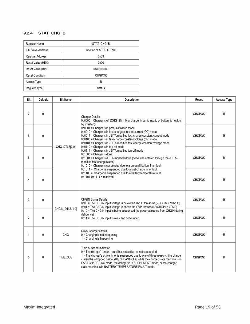
9.2.4 STAT_CHG_B
Register Name STAT_CHG_B
I2C Slave Address function of ADDR OTP bit
Register Address 0x03
Reset Value (HEX) 0x00
Reset Value (BIN) 0b00000000
Reset Condition CHGPOK
Access Type R
Register Type Status
Bit Default Bit Name Description Reset Access Type
7 0
CHG_DTLS[3:0]
Charger Details 0b0000 = Charger is off (CHG_EN = 0 or charger input is invalid or battery is not low by Vrestart) 0b0001 = Charger is in prequalification mode 0b0010 = Charger is in fast-charge constant-current (CC) mode 0b0011 = Charger is in JEITA modified fast-charge constant-current mode 0b0100 = Charger is in fast-charge constant-voltage (CV) mode 0b0101 = Charger is in JEITA modified fast-charge constant-voltage mode 0b0110 = Charger is in top-off mode 0b0111 = Charger is in JEITA modified top-off mode 0b1000 = Charger is done 0b1001 = Charger is JEITA modified done (done was entered through the JEITA-modified fast-charge states) 0b1010 = Charger is suspended due to a prequalification timer fault 0b1011 = Charger is suspended due to a fast-charge timer fault 0b1100 = Charger is suspended due to a battery temperature fault 0b1101-0b1111 = reserved
CHGPOK R
6 0 CHGPOK R
5 0 CHGPOK R
4 0 CHGPOK R
3 0
CHGIN_DTLS[1:0]
CHGIN Status Details 0b00 = The CHGIN input voltage is below the UVLO threshold (VCHGIN < VUVLO) 0b01 = The CHGIN input voltage is above the OVP threshold (VCHGIN > VOVP) 0b10 = The CHGIN input is being debounced (no power accepted from CHGIN during debounce) 0b11 = The CHGIN input is okay and debounced
CHGPOK R
2 0 CHGPOK R
1 0 CHG Quick Charger Status 0 = Charging is not happening 1 = Charging is happening
CHGPOK R
0 0 TIME_SUS
Time Suspend Indicator 0 = The charger's timers are either not active, or not suspended 1 = The charger's active timer is suspended due to one of three reasons: the charge current has dropped below 20% of IFAST-CHG while the charger state machine is in FAST CHARGE CC mode, the charger is in SUPPLIMENT mode, or the charger state machine is in BATTERY TEMPERATURE FAULT mode.
CHGPOK R

Maxim Integrated Page 20 of 53
9.2.5 CNFG_CHG_A
Register Name CNFG_CHG_A
I2C Slave Address function of ADDR OTP bit
Register Address 0x18
Reset Value (HEX) 0x0F
Reset Value (BIN) 0b00001111
Reset Condition SYSRST=1
Access Type R/W
Register Type Configuration
Bit Default Bit Name Description Reset Access Type
7 0
THM_HOT[1:0]
Sets the VHOT JEITA Temperature Threshold 0b00 = VHOT = 0.411V 0b01 = VHOT = 0.367V 0b10 = VHOT = 0.327V 0b11 = VHOT = 0.291V
SYSRST=1 R/W
6 0 SYSRST=1 R/W
5 0
THM_WARM[1:0]
Sets the VWARM JEITA Temperature Threshold 0b00 = VWARM = 0.511V 0b01 = VWARM = 0.459V 0b10 = VWARM = 0.411V 0b11 = VWARM = 0.367V
SYSRST=1 R/W
4 0 SYSRST=1 R/W
3 1
THM_COOL[1:0]
Sets the VCOOL JEITA Temperature Threshold 0b00 = VCOOL = 0.923V 0b01 = VCOOL = 0.867V 0b10 = VCOOL = 0.807V 0b11 = VCOOL = 0.747V
SYSRST=1 R/W
2 1 SYSRST=1 R/W
1 1
THM_COLD[1:0]
Sets the VCOLD JEITA Temperature Threshold 0b00 = VCOLD = 1.024V 0b01 = VCOLD = 0.976V 0b10 = VCOLD = 0.923V 0b11 = VCOLD = 0.867V
SYSRST=1 R/W
0 1 SYSRST=1 R/W
Maxim Integrated Page 21 of 53
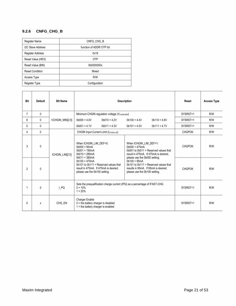
9.2.6 CNFG_CHG_B
Register Name CNFG_CHG_B
I2C Slave Address function of ADDR OTP bit
Register Address 0x19
Reset Value (HEX) OTP
Reset Value (BIN) 0b0000000x
Reset Condition Mixed
Access Type R/W
Register Type Configuration
Bit Default Bit Name Description Reset Access Type
7 0
VCHGIN_MIN[2:0]
Minimum CHGIN regulation voltage (VCHGIN-MIN) SYSRST=1 R/W
6 0 0b000 = 4.0V 0b010 = 4.2V 0b100 = 4.4V 0b110 = 4.6V SYSRST=1 R/W
5 0 0b001 = 4.1V 0b011 = 4.3V 0b101 = 4.5V 0b111 = 4.7V SYSRST=1 R/W
4 0
ICHGIN_LIM[2:0]
CHGIN Input Current Limit (ICHGIN-LIM) CHGPOK R/W
3 0 When ICHGIN_LIM_DEF=0: 0b000 = 95mA 0b001 = 190mA 0b010 = 285mA 0b011 = 380mA 0b100 = 475mA 0b101 to 0b111 = Reserved values that result in 475mA. If 475mA is desired, please use the 0b100 setting.
When ICHGIN_LIM_DEF=1: 0b000 = 475mA 0b001 to 0b011 = Reserved values that result in 475mA. If 475mA is desired, please use the 0b000 setting. 0b100 = 95mA 0b101 to 0b111 = Reserved values that results in 95mA. If 95mA is desired, please use the 0b100 setting.
CHGPOK R/W
2 0 CHGPOK R/W
1 0 I_PQ Sets the prequalification charge current (IPQ) as a percentage of IFAST-CHG 0 = 10% 1 = 20%
SYSRST=1 R/W
0 x CHG_EN Charger Enable 0 = the battery charger is disabled 1 = the battery charger is enabled
SYSRST=1 R/W

Maxim Integrated Page 22 of 53
9.2.7 CNFG_CHG_C
Register Name CNFG_CHG_C
I2C Slave Address function of ADDR OTP bit
Register Address 0x1A
Reset Value (HEX) 0xF8
Reset Value (BIN) 0b11111000
Reset Condition SYSRST=1
Access Type R/W
Register Type Configuration
Bit Default Bit Name Description Reset Access Type
7 1
CHG_PQ[2:0]
Battery prequalification voltage threshold (VPQ) SYSRST=1 R/W
6 1 0b000 = 2.3V 0b010 = 2.5V 0b100 = 2.7V 0b110 = 2.9V SYSRST=1 R/W
5 1 0b001 = 2.4V 0b011 = 2.6V 0b101 = 2.8V 0b111 = 3.0V SYSRST=1 R/W
4 1
I_TERM[1:0]
Charger Termination Current (ITERM). I_TERM[1:0] sets the charger termination current as a percentage of the fast charge current IFAST-CHG. 00 = 5% 01 = 7.5% 10 = 10% 11 = 15%
SYSRST=1 R/W
3 1 SYSRST=1 R/W
2 0
T_TOPOFF[2:0]
Topoff timer value (tTO) SYSRST=1 R/W
1 0 0b000 = 0 minutes 0b010 = 10 minutes
0b100 = 20 minutes
0b110 = 30 minutes
SYSRST=1 R/W
0 0 0b001 = 5 minutes 0b011 = 15 minutes
0b101 = 25 minutes
0b111 = 35 minutes
SYSRST=1 R/W
Maxim Integrated Page 23 of 53
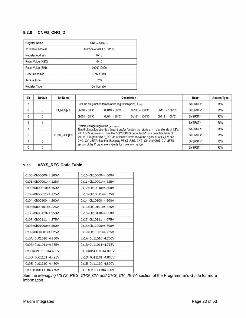
9.2.8 CNFG_CHG_D
Register Name CNFG_CHG_D
I2C Slave Address function of ADDR OTP bit
Register Address 0x1B
Reset Value (HEX) 0x10
Reset Value (BIN) 0b00010000
Reset Condition SYSRST=1
Access Type R/W
Register Type Configuration
Bit Default Bit Name Description Reset Access Type
7 0
TJ_REG[2:0]
Sets the die junction temperature regulation point, TJ-REG SYSRST=1 R/W
6 0 0b000 = 60°C 0b010 = 80°C 0b100 = 100°C 0b110 = 100°C SYSRST=1 R/W
5 0 0b001 = 70°C 0b011 = 90°C 0b101 = 100°C 0b111 = 100°C SYSRST=1 R/W
4 1
VSYS_REG[4:0]
System voltage regulation (VSYS-REG) This 5-bit configuration is a linear transfer function that starts at 4.1V and ends at 4.8V, with 25mV increments. See the "VSYS_REG Code Table" for a complete table of values. Program VSYS_REG to at least 200mV above the higher of CHG_CV and CHG_CV_JEITA. See the Managing VSYS_REG, CHG_CV, and CHG_CV_JEITA section of the Programmer's Guide for more information.
SYSRST=1 R/W
3 0 SYSRST=1 R/W
2 0 SYSRST=1 R/W
1 0 SYSRST=1 R/W
0 0 SYSRST=1 R/W
9.2.9 VSYS_REG Code Table
0x00=0b00000=4.100V 0x10=0b10000=4.500V
0x01=0b00001=4.125V 0x11=0b10001=4.525V
0x02=0b00010=4.150V 0x12=0b10010=4.550V
0x03=0b00011=4.175V 0x13=0b10011=4.575V
0x04=0b00100=4.200V 0x14=0b10100=4.600V
0x05=0b00101=4.225V 0x15=0b10101=4.625V
0x06=0b00110=4.250V 0x16=0b10110=4.650V
0x07=0b00111=4.275V 0x17=0b10111=4.675V
0x08=0b01000=4.300V 0x18=0b11000=4.700V
0x09=0b01001=4.325V 0x19=0b11001=4.725V
0x0A=0b01010=4.350V 0x1A=0b11010=4.750V
0x0B=0b01011=4.375V 0x1B=0b11011=4.775V
0x0C=0b01100=4.400V 0x1C=0b11100=4.800V
0x0D=0b01101=4.425V 0x1D=0b11101=4.800V
0x0E=0b01110=4.450V 0x1E=0b11110=4.800V
0x0F=0b01111=4.475V 0x1F=0b11111=4.800V
See the Managing VSYS_REG, CHG_CV, and CHG_CV_JEITA section of the Programmer’s Guide for more information.

Maxim Integrated Page 24 of 53
9.2.10 CNFG_CHG_E
Register Name CNFG_CHG_E
I2C Slave Address function of ADDR OTP bit
Register Address 0x1C
Reset Value (HEX) 0x05
Reset Value (BIN) 0b00000101
Reset Condition SYSRST=1
Access Type R/W
Register Type Configuration
Bit Default Bit Name Description Reset Access Type
7 0
CHG_CC[5:0]
Sets the fast-charge constant current value, IFAST-CHG. This 6-bit configuration is a linear transfer function that starts at 7.5mA and ends at 300mA, with 7.5mA increments. See the "CHG_CC Code Table" for a complete table of values.
SYSRST=1 R/W
6 0 SYSRST=1 R/W
5 0 SYSRST=1 R/W
4 0 SYSRST=1 R/W
3 0 SYSRST=1 R/W
2 1 SYSRST=1 R/W
1 0
T_FAST_CHG[1:0]
Sets the fast-charge safety timer, tFC. 0b00 = timer disabled 0b01 = 3 hours 0b10 = 5 hours 0b11 = 7 hours
SYSRST=1 R/W
0 1 SYSRST=1 R/W

Maxim Integrated Page 25 of 53
9.2.11 CHG_CC and CHG_CC_JEITA Code Table
0x00=0b000000=7.5mA 0x10=0b010000=127.5mA 0x20=0b100000=247.5mA 0x30=0b110000=300.0mA
0x01=0b000001=15.0mA 0x11=0b010001=135.0mA 0x21=0b100001=255.0mA 0x31=0b110001=300.0mA
0x02=0b000010=22.5mA 0x12=0b010010=142.5mA 0x22=0b100010=262.5mA 0x32=0b110010=300.0mA
0x03=0b000011=30.0mA 0x13=0b010011=150.0mA 0x23=0b100011=270.0mA 0x33=0b110011=300.0mA
0x04=0b000100=37.5mA 0x14=0b010100=157.5mA 0x24=0b100100=277.5mA 0x34=0b110100=300.0mA
0x05=0b000101=45.0mA 0x15=0b010101=165.0mA 0x25=0b100101=285.0mA 0x35=0b110101=300.0mA
0x06=0b000110=52.5mA 0x16=0b010110=172.5mA 0x26=0b100110=292.5mA 0x36=0b110110=300.0mA
0x07=0b000111=60.0mA 0x17=0b010111=180.0mA 0x27=0b100111=300.0mA 0x37=0b110111=300.0mA
0x08=0b001000=67.5mA 0x18=0b011000=187.5mA 0x28=0b101000=300.0mA 0x38=0b111000=300.0mA
0x09=0b001001=75.0mA 0x19=0b011001=195.0mA 0x29=0b101001=300.0mA 0x39=0b111001=300.0mA
0x0A=0b001010=82.5mA 0x1A=0b011010=202.5mA 0x2A=0b101010=300.0mA 0x3A=0b111010=300.0mA
0x0B=0b001011=90.0mA 0x1B=0b011011=210.0mA 0x2B=0b101011=300.0mA 0x3B=0b111011=300.0mA
0x0C=0b001100=97.5mA 0x1C=0b011100=217.5mA 0x2C=0b101100=300.0mA 0x3C=0b111100=300.0mA
0x0D=0b001101=105.0mA 0x1D=0b011101=225.0mA 0x2D=0b101101=300.0mA 0x3D=0b111101=300.0mA
0x0E=0b001110=112.5mA 0x1E=0b011110=232.5mA 0x2E=0b101110=300.0mA 0x3E=0b111110=300.0mA
0x0F=0b001111=120.0mA 0x1F=0b011111=240.0mA 0x2F=0b101111=300.0mA 0x3F=0b111111=300.0mA

Maxim Integrated Page 26 of 53
9.2.12 CNFG_CHG_F
Register Name CNFG_CHG_F
I2C Slave Address function of ADDR OTP bit
Register Address 0x1D
Reset Value (HEX) 0x04
Reset Value (BIN) 0b00000100
Reset Condition SYSRST=1
Access Type R/W
Register Type Configuration
Bit Default Bit Name Description Reset Access Type
7 0
CHG_CC_JEITA[5:0]
Sets IFAST-CHG_JEITA for when the battery is either cool or warm as defined by the TCOOL and TWARM temperature thresholds. This register is a don't care if the battery temperature is normal. This 6-bit configuration is a linear transfer function that starts at 7.5mA and ends at 300mA, with 7.5mA increments. See the "CHG_CC Code Table" for a complete table of values.
SYSRST=1 R/W
6 0 SYSRST=1 R/W
5 0 SYSRST=1 R/W
4 0 SYSRST=1 R/W
3 0 SYSRST=1 R/W
2 1 SYSRST=1 R/W
1 0 THM_EN
Thermistor enable bit 0 = The charger does not enable the thermistor bias and battery temperature is ignored by charger logic 1 = The charger enables the thermistor and continuously monitors battery temperature
SYSRST=1 R/W
0 0 RESERVED Reserved. This bit is reserved. Writes to this bit should be 0. SYSRST=1 R/W
Maxim Integrated Page 27 of 53
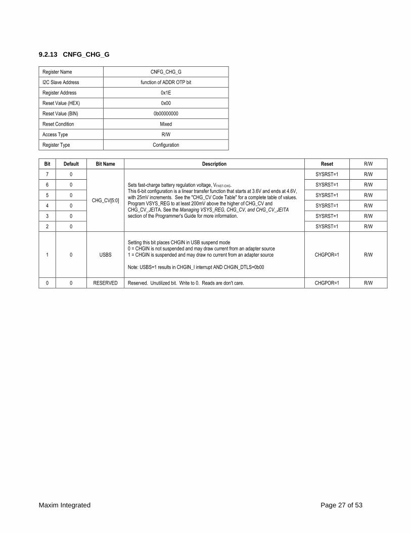
9.2.13 CNFG_CHG_G
Register Name CNFG_CHG_G
I2C Slave Address function of ADDR OTP bit
Register Address 0x1E
Reset Value (HEX) 0x00
Reset Value (BIN) 0b00000000
Reset Condition Mixed
Access Type R/W
Register Type Configuration
Bit Default Bit Name Description Reset R/W
7 0
CHG_CV[5:0]
Sets fast-charge battery regulation voltage, VFAST-CHG. This 6-bit configuration is a linear transfer function that starts at 3.6V and ends at 4.6V, with 25mV increments. See the "CHG_CV Code Table" for a complete table of values. Program VSYS_REG to at least 200mV above the higher of CHG_CV and CHG_CV_JEITA. See the Managing VSYS_REG, CHG_CV, and CHG_CV_JEITA section of the Programmer's Guide for more information.
SYSRST=1 R/W
6 0 SYSRST=1 R/W
5 0 SYSRST=1 R/W
4 0 SYSRST=1 R/W
3 0 SYSRST=1 R/W
2 0 SYSRST=1 R/W
1 0 USBS
Setting this bit places CHGIN in USB suspend mode 0 = CHGIN is not suspended and may draw current from an adapter source 1 = CHGIN is suspended and may draw no current from an adapter source Note: USBS=1 results in CHGIN_I interrupt AND CHGIN_DTLS=0b00
CHGPOR=1 R/W
0 0 RESERVED Reserved. Unutilized bit. Write to 0. Reads are don't care. CHGPOR=1 R/W

Maxim Integrated Page 28 of 53
9.2.14 CHG_CV and CHG_CV_JEITA Code Table
0x00=0b000000=3.600V 0x10=0b010000=4.000V 0x20=0b100000=4.400V 0x30=0b110000=4.600V
0x01=0b000001=3.625V 0x11=0b010001=4.025V 0x21=0b100001=4.425V 0x31=0b110001=4.600V
0x02=0b000010=3.650V 0x12=0b010010=4.050V 0x22=0b100010=4.450V 0x32=0b110010=4.600V
0x03=0b000011=3.675V 0x13=0b010011=4.075V 0x23=0b100011=4.475V 0x33=0b110011=4.600V
0x04=0b000100=3.700V 0x14=0b010100=4.100V 0x24=0b100100=4.500V 0x34=0b110100=4.600V
0x05=0b000101=3.725V 0x15=0b010101=4.125V 0x25=0b100101=4.525V 0x35=0b110101=4.600V
0x06=0b000110=3.750V 0x16=0b010110=4.150V 0x26=0b100110=4.550V 0x36=0b110110=4.600V
0x07=0b000111=3.775V 0x17=0b010111=4.175V 0x27=0b100111=4.575V 0x37=0b110111=4.600V
0x08=0b001000=3.800V 0x18=0b011000=4.200V 0x28=0b101000=4.600V 0x38=0b111000=4.600V
0x09=0b001001=3.825V 0x19=0b011001=4.225V 0x29=0b101001=4.600V 0x39=0b111001=4.600V
0x0A=0b001010=3.850V 0x1A=0b011010=4.250V 0x2A=0b101010=4.600V 0x3A=0b111010=4.600V
0x0B=0b001011=3.875V 0x1B=0b011011=4.275V 0x2B=0b101011=4.600V 0x3B=0b111011=4.600V
0x0C=0b001100=3.900V 0x1C=0b011100=4.300V 0x2C=0b101100=4.600V 0x3C=0b111100=4.600V
0x0D=0b001101=3.925V 0x1D=0b011101=4.325V 0x2D=0b101101=4.600V 0x3D=0b111101=4.600V
0x0E=0b001110=3.950V 0x1E=0b011110=4.350V 0x2E=0b101110=4.600V 0x3E=0b111110=4.600V
0x0F=0b001111=3.975V 0x1F=0b011111=4.375V 0x2F=0b101111=4.600V 0x3F=0b111111=4.600V
See the Managing VSYS_REG, CHG_CV, and CHG_CV_JEITA section of the Programmer’s Guide for more information.
Maxim Integrated Page 29 of 53
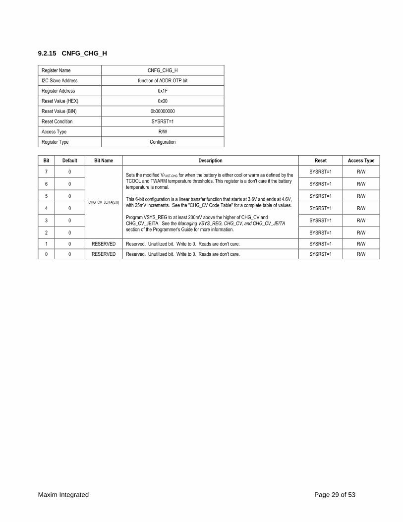
9.2.15 CNFG_CHG_H
Register Name CNFG_CHG_H
I2C Slave Address function of ADDR OTP bit
Register Address 0x1F
Reset Value (HEX) 0x00
Reset Value (BIN) 0b00000000
Reset Condition SYSRST=1
Access Type R/W
Register Type Configuration
Bit Default Bit Name Description Reset Access Type
7 0
CHG_CV_JEITA[5:0]
Sets the modified VFAST-CHG for when the battery is either cool or warm as defined by the TCOOL and TWARM temperature thresholds. This register is a don't care if the battery temperature is normal. This 6-bit configuration is a linear transfer function that starts at 3.6V and ends at 4.6V, with 25mV increments. See the "CHG_CV Code Table" for a complete table of values. Program VSYS_REG to at least 200mV above the higher of CHG_CV and CHG_CV_JEITA. See the Managing VSYS_REG, CHG_CV, and CHG_CV_JEITA section of the Programmer's Guide for more information.
SYSRST=1 R/W
6 0 SYSRST=1 R/W
5 0 SYSRST=1 R/W
4 0 SYSRST=1 R/W
3 0 SYSRST=1 R/W
2 0 SYSRST=1 R/W
1 0 RESERVED Reserved. Unutilized bit. Write to 0. Reads are don't care. SYSRST=1 R/W
0 0 RESERVED Reserved. Unutilized bit. Write to 0. Reads are don't care. SYSRST=1 R/W
Maxim Integrated Page 30 of 53
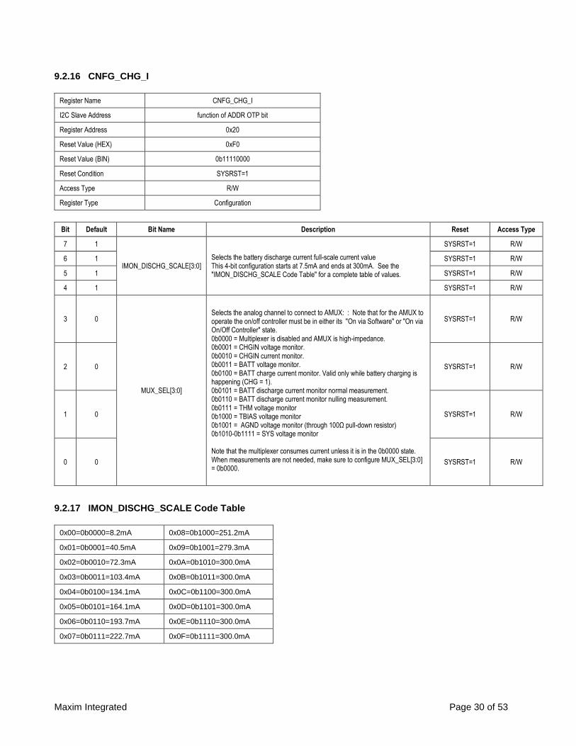
9.2.16 CNFG_CHG_I
Register Name CNFG_CHG_I
I2C Slave Address function of ADDR OTP bit
Register Address 0x20
Reset Value (HEX) 0xF0
Reset Value (BIN) 0b11110000
Reset Condition SYSRST=1
Access Type R/W
Register Type Configuration
Bit Default Bit Name Description Reset Access Type
7 1
IMON_DISCHG_SCALE[3:0] Selects the battery discharge current full-scale current value This 4-bit configuration starts at 7.5mA and ends at 300mA. See the "IMON_DISCHG_SCALE Code Table" for a complete table of values.
SYSRST=1 R/W
6 1 SYSRST=1 R/W
5 1 SYSRST=1 R/W
4 1 SYSRST=1 R/W
3 0
MUX_SEL[3:0]
Selects the analog channel to connect to AMUX: : Note that for the AMUX to operate the on/off controller must be in either its "On via Software" or "On via On/Off Controller" state. 0b0000 = Multiplexer is disabled and AMUX is high-impedance. 0b0001 = CHGIN voltage monitor. 0b0010 = CHGIN current monitor. 0b0011 = BATT voltage monitor. 0b0100 = BATT charge current monitor. Valid only while battery charging is happening (CHG = 1). 0b0101 = BATT discharge current monitor normal measurement. 0b0110 = BATT discharge current monitor nulling measurement. 0b0111 = THM voltage monitor 0b1000 = TBIAS voltage monitor 0b1001 = AGND voltage monitor (through 100Ω pull-down resistor) 0b1010-0b1111 = SYS voltage monitor Note that the multiplexer consumes current unless it is in the 0b0000 state. When measurements are not needed, make sure to configure MUX_SEL[3:0] = 0b0000.
SYSRST=1 R/W
2 0 SYSRST=1 R/W
1 0 SYSRST=1 R/W
0 0 SYSRST=1 R/W
9.2.17 IMON_DISCHG_SCALE Code Table
0x00=0b0000=8.2mA 0x08=0b1000=251.2mA
0x01=0b0001=40.5mA 0x09=0b1001=279.3mA
0x02=0b0010=72.3mA 0x0A=0b1010=300.0mA
0x03=0b0011=103.4mA 0x0B=0b1011=300.0mA
0x04=0b0100=134.1mA 0x0C=0b1100=300.0mA
0x05=0b0101=164.1mA 0x0D=0b1101=300.0mA
0x06=0b0110=193.7mA 0x0E=0b1110=300.0mA
0x07=0b0111=222.7mA 0x0F=0b1111=300.0mA

Maxim Integrated Page 31 of 53
9.3 Register Descriptions: LDO
9.3.1 CNFG_LDO_A
Register Name CNFG_LDO_A
I2C Slave Address function of ADDR OTP bit
Register Address 0x38
Reset Value (HEX) OTP
Reset Value (BIN) 0bxxxxxxxx
Reset Condition SYSRST=1
Access Type R/W
Register Type Configuration
Bit Default Bit Name Description Reset Access Type
7 x RESERVED Reserved. Unutilized bit. Write to 0. Reads are don't care. SYSRST=1 R/W
6 x
TV_LDO[6:0]
LDO Target Output Voltage This 7-bit configuration is a linear transfer function that starts at 1.35V and ends at 2.9375V, with 12.5mV increments. See the "TV_LDO" tab in this spreadsheet for a complete table of values.
SYSRST=1 R/W
5 x SYSRST=1 R/W
4 x SYSRST=1 R/W
3 x SYSRST=1 R/W
2 x SYSRST=1 R/W
1 x SYSRST=1 R/W
0 x SYSRST=1 R/W

Maxim Integrated Page 32 of 53
9.3.2 TV_LDO Code Table
0x00=0b0000000=1.3500V 0x20=0b0100000=1.7500V 0x40=0b1000000=2.1500V 0x60=0b1100000=2.5500V
0x01=0b0000001=1.3625V 0x21=0b0100001=1.7625V 0x41=0b1000001=2.1625V 0x61=0b1100001=2.5625V
0x02=0b0000010=1.3750V 0x22=0b0100010=1.7750V 0x42=0b1000010=2.1750V 0x62=0b1100010=2.5750V
0x03=0b0000011=1.3875V 0x23=0b0100011=1.7875V 0x43=0b1000011=2.1875V 0x63=0b1100011=2.5875V
0x04=0b0000100=1.4000V 0x24=0b0100100=1.8000V 0x44=0b1000100=2.2000V 0x64=0b1100100=2.6000V
0x05=0b0000101=1.4125V 0x25=0b0100101=1.8125V 0x45=0b1000101=2.2125V 0x65=0b1100101=2.6125V
0x06=0b0000110=1.4250V 0x26=0b0100110=1.8250V 0x46=0b1000110=2.2250V 0x66=0b1100110=2.6250V
0x07=0b0000111=1.4375V 0x27=0b0100111=1.8375V 0x47=0b1000111=2.2375V 0x67=0b1100111=2.6375V
0x08=0b0001000=1.4500V 0x28=0b0101000=1.8500V 0x48=0b1001000=2.2500V 0x68=0b1101000=2.6500V
0x09=0b0001001=1.4625V 0x29=0b0101001=1.8625V 0x49=0b1001001=2.2625V 0x69=0b1101001=2.6625V
0x0A=0b0001010=1.4750V 0x2A=0b0101010=1.8750V 0x4A=0b1001010=2.2750V 0x6A=0b1101010=2.6750V
0x0B=0b0001011=1.4875V 0x2B=0b0101011=1.8875V 0x4B=0b1001011=2.2875V 0x6B=0b1101011=2.6875V
0x0C=0b0001100=1.5000V 0x2C=0b0101100=1.9000V 0x4C=0b1001100=2.3000V 0x6C=0b1101100=2.7000V
0x0D=0b0001101=1.5125V 0x2D=0b0101101=1.9125V 0x4D=0b1001101=2.3125V 0x6D=0b1101101=2.7125V
0x0E=0b0001110=1.5250V 0x2E=0b0101110=1.9250V 0x4E=0b1001110=2.3250V 0x6E=0b1101110=2.7250V
0x0F=0b0001111=1.5375V 0x2F=0b0101111=1.9375V 0x4F=0b1001111=2.3375V 0x6F=0b1101111=2.7375V
0x10=0b0010000=1.5500V 0x30=0b0110000=1.9500V 0x50=0b1010000=2.3500V 0x70=0b1110000=2.7500V
0x11=0b0010001=1.5625V 0x31=0b0110001=1.9625V 0x51=0b1010001=2.3625V 0x71=0b1110001=2.7625V
0x12=0b0010010=1.5750V 0x32=0b0110010=1.9750V 0x52=0b1010010=2.3750V 0x72=0b1110010=2.7750V
0x13=0b0010011=1.5875V 0x33=0b0110011=1.9875V 0x53=0b1010011=2.3875V 0x73=0b1110011=2.7875V
0x14=0b0010100=1.6000V 0x34=0b0110100=2.0000V 0x54=0b1010100=2.4000V 0x74=0b1110100=2.8000V
0x15=0b0010101=1.6125V 0x35=0b0110101=2.0125V 0x55=0b1010101=2.4125V 0x75=0b1110101=2.8125V
0x16=0b0010110=1.6250V 0x36=0b0110110=2.0250V 0x56=0b1010110=2.4250V 0x76=0b1110110=2.8250V
0x17=0b0010111=1.6375V 0x37=0b0110111=2.0375V 0x57=0b1010111=2.4375V 0x77=0b1110111=2.8375V
0x18=0b0011000=1.6500V 0x38=0b0111000=2.0500V 0x58=0b1011000=2.4500V 0x78=0b1111000=2.8500V
0x19=0b0011001=1.6625V 0x39=0b0111001=2.0625V 0x59=0b1011001=2.4625V 0x79=0b1111001=2.8625V
0x1A=0b0011010=1.6750V 0x3A=0b0111010=2.0750V 0x5A=0b1011010=2.4750V 0x7A=0b1111010=2.8750V
0x1B=0b0011011=1.6875V 0x3B=0b0111011=2.0875V 0x5B=0b1011011=2.4875V 0x7B=0b1111011=2.8875V
0x1C=0b0011100=1.7000V 0x3C=0b0111100=2.1000V 0x5C=0b1011100=2.5000V 0x7C=0b1111100=2.9000V
0x1D=0b0011101=1.7125V 0x3D=0b0111101=2.1125V 0x5D=0b1011101=2.5125V 0x7D=0b1111101=2.9125V
0x1E=0b0011110=1.7250V 0x3E=0b0111110=2.1250V 0x5E=0b1011110=2.5250V 0x7E=0b1111110=2.9250V
0x1F=0b0011111=1.7375V 0x3F=0b0111111=2.1375V 0x5F=0b1011111=2.5375V 0x7F=0b1111111=2.9375V

Maxim Integrated Page 33 of 53
9.3.3 CNFG_LDO_B
Register Name CNFG_LDO_B
I2C Slave Address function of ADDR OTP bit
Register Address 0x39
Reset Value (HEX) OTP
Reset Value (BIN) 0b0000xxxx
Reset Condition SYSRST=1
Access Type R/W
Register Type Configuration
Bit Default Bit Name Description Reset Access Type
7 0 BLANK Blank. There is no bit at this location. Write to 0. Reads are don't care. SYSRST=1 R/W
6 0 BLANK Blank. There is no bit at this location. Write to 0. Reads are don't care. SYSRST=1 R/W
5 0 BLANK Blank. There is no bit at this location. Write to 0. Reads are don't care. SYSRST=1 R/W
4 0 BLANK Blank. There is no bit at this location. Write to 0. Reads are don't care. SYSRST=1 R/W
3 x ADE_LDO
LDO active-Discharge Enable 0=The active discharge function is disabled. When LDO is disabled, it's discharge rate is a function of the output capacitance and the external load. 1=The active discharge function is enabled. When LDO is disabled, an internal resistor (RAD_LDO) is activated from LDO to GND to help the output voltage discharge. The output voltage discharge rate is a function of the output capacitance, the external loading, and the internal RAD_LDO load.
SYSRST=1 R/W
2 x
EN_LDO[2:0]
Enable Control for LDO. 0b000 = LDO powers-up and powers-down in FPS slot 0 0b001 = LDO powers-up and powers-down in FPS slot 1 0b010 = LDO powers-up and powers-down in FPS slot 2 0b011 = LDO powers-up and powers-down in FPS slot 3 0b100 = LDO is off irrespective of FPS 0b101 = same as 0b100 0b110 = LDO is on irrespective of FPS whenever the on/off controller is in its "On via Software" or "On via On/Off Controller" states. 0b111 = same as 0b110
SYSRST=1 R/W
1 x SYSRST=1 R/W
0 x SYSRST=1 R/W

Maxim Integrated Page 34 of 53
9.4 Register Descriptions: SIMO Buck Boost
9.4.1 CNFG_SBB_TOP
Register Name CNFG_SBB_TOP
I2C Slave Address function of ADDR OTP bit
Register Address 0x28
Reset Value (HEX) OTP
Reset Value (BIN) 0bxxxxxxxx
Reset Condition SYSRST=1
Access Type R/W
Register Type Configuration
Bit Default Bit Name Description Reset Access Type
7 x RESERVED Reserved. Unutilized bit. Write to 0. Reads are don't care. SYSRST=1 R/W
6 x MRT_OTP
Manual Reset Time Configuration 0 = the manual reset time (tMRST) is typically 16s 1 = The manual reset time (tMRST) is typically 8s Note that the default value of this bit controls the manual reset time. This bit can be written to its alternate value but does not change the manual reset time configuration. When writing to this register, it is recommended to leave this bit in its default configuration.
SYSRST=1 R/W
5 x SBIA_LPM_DEF
Default voltage of the SBIA_LPM bit 0 = SBIA_LPM defaults to 0 which gives the normal power mode 1 = SBIA_LPM defaults to 1 which gives the low power mode Note that the default value of this bit controls the default value of SBIA_LPM. This bit can be written to its alternate value but does not change the bias power mode. If software needs to change the bias power mode, it should program the SBIA_LPM bit directly. When writing to this register, it is recommended to leave this bit in its default configuration.
SYSRST=1 R/W
4 x DBNC_nEN_DEF
Default Value of the DBNC_nEN bit 0 = DBNC_nEN defaults to 0 which gives a 100us nEN debounce time 1 = DBNC_nEN defaults to 1 which gives a 30ms nEN debounce time Note that the default value of this bit controls the default value of DBNC_nEN. This bit can be written to its alternate value but does not change the nEN debounce time. If software needs to change the DBNC_nEN debounce time, it should program the DBNC_nEN bit directly. When writing to this register, it is recommended to leave this bit in its default configuration.
SYSRST=1 R/W
3 x RESERVED Reserved. These bits are reserved. Write to 0x00.
SYSRST=1 R/W
2 x SYSRST=1 R/W

Maxim Integrated Page 35 of 53
1 x
DRV_SBB[1:0]
SIMO Buck-Boost (all channels) Drive Strength Trim. The ideal value of this register should be determined experimentally for each platform. The 0b01 setting is the best setting for a PCB layout that is comparable to maxim's own EVKIT and represents a balance between efficiency and EMI. The faster setting can result in higher efficiency but generally requires a tighter EVKIT layout or shielding to avoid addition EMI. Slower settings allow for controlling EMI in non-ideal setting (i.e. contained layout, antenna adjacent to device . . . etc.). This setting is intended to be set once by the initialization code within a system. 0b00=fastest transition time 0b01=a little slower than 0b00 0b10=a little slower than 0b01 0b11=a little slower than 0b10
SYSRST=1 R/W
0 x SYSRST=1 R/W

Maxim Integrated Page 36 of 53
9.4.2 CNFG_SBB0_A
Register Name CNFG_SBB0_A
I2C Slave Address function of ADDR OTP bit
Register Address 0x29
Reset Value (HEX) OTP
Reset Value (BIN) 0bxxxxxxxx
Reset Condition SYSRST=1
Access Type R/W
Register Type Configuration
Bit Default Bit Name Description Reset Access Type
7 x
IP_SBB0[1:0]
SIMO Buck-Boost Channel 1 Peak Current Limit 0b00=1.000A 0b01=0.866A 0b10=0.707A 0b11=0.500A
SYSRST=1 R/W
6 x SYSRST=1 R/W
5 x
TV_SBB0[5:0]
SIMO Buck-Boost Channel 0 Target Output Voltage This 6-bit configuration is a linear transfer function that starts at 0.8V, ends at 2.375V, with 25mV increments. See the "TV_SBBx" tab in this spreadsheet for a complete table of values.
SYSRST=1 R/W
4 x SYSRST=1 R/W
3 x SYSRST=1 R/W
2 x SYSRST=1 R/W
1 x SYSRST=1 R/W
0 x SYSRST=1 R/W
9.4.3 TV_SBB0 Code Table
0x00=0b000000=0.800V 0x10=0b010000=1.200V 0x20=0b100000=1.600V 0x30=0b110000=2.000V
0x01=0b000001=0.825V 0x11=0b010001=1.225V 0x21=0b100001=1.625V 0x31=0b110001=2.025V
0x02=0b000010=0.850V 0x12=0b010010=1.250V 0x22=0b100010=1.650V 0x32=0b110010=2.050V
0x03=0b000011=0.875V 0x13=0b010011=1.275V 0x23=0b100011=1.675V 0x33=0b110011=2.075V
0x04=0b000100=0.900V 0x14=0b010100=1.300V 0x24=0b100100=1.700V 0x34=0b110100=2.100V
0x05=0b000101=0.925V 0x15=0b010101=1.325V 0x25=0b100101=1.725V 0x35=0b110101=2.125V
0x06=0b000110=0.950V 0x16=0b010110=1.350V 0x26=0b100110=1.750V 0x36=0b110110=2.150V
0x07=0b000111=0.975V 0x17=0b010111=1.375V 0x27=0b100111=1.775V 0x37=0b110111=2.175V
0x08=0b001000=1.000V 0x18=0b011000=1.400V 0x28=0b101000=1.800V 0x38=0b111000=2.200V
0x09=0b001001=1.025V 0x19=0b011001=1.425V 0x29=0b101001=1.825V 0x39=0b111001=2.225V
0x0A=0b001010=1.050V 0x1A=0b011010=1.450V 0x2A=0b101010=1.850V 0x3A=0b111010=2.250V
0x0B=0b001011=1.075V 0x1B=0b011011=1.475V 0x2B=0b101011=1.875V 0x3B=0b111011=2.275V
0x0C=0b001100=1.100V 0x1C=0b011100=1.500V 0x2C=0b101100=1.900V 0x3C=0b111100=2.300V
0x0D=0b001101=1.125V 0x1D=0b011101=1.525V 0x2D=0b101101=1.925V 0x3D=0b111101=2.325V
0x0E=0b001110=1.150V 0x1E=0b011110=1.550V 0x2E=0b101110=1.950V 0x3E=0b111110=2.350V
0x0F=0b001111=1.175V 0x1F=0b011111=1.575V 0x2F=0b101111=1.975V 0x3F=0b111111=2.375V
Maxim Integrated Page 37 of 53
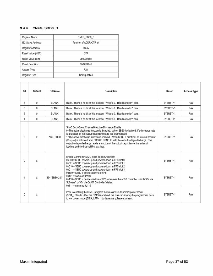
9.4.4 CNFG_SBB0_B
Register Name CNFG_SBB0_B
I2C Slave Address function of ADDR OTP bit
Register Address 0x2A
Reset Value (HEX) OTP
Reset Value (BIN) 0b0000xxxx
Reset Condition SYSRST=1
Access Type R/W
Register Type Configuration
Bit Default Bit Name Description Reset Access Type
7 0 BLANK Blank. There is no bit at this location. Write to 0. Reads are don't care. SYSRST=1 R/W
6 0 BLANK Blank. There is no bit at this location. Write to 0. Reads are don't care. SYSRST=1 R/W
5 0 BLANK Blank. There is no bit at this location. Write to 0. Reads are don't care. SYSRST=1 R/W
4 0 BLANK Blank. There is no bit at this location. Write to 0. Reads are don't care. SYSRST=1 R/W
3 x ADE_SBB0
SIMO Buck-Boost Channel 0 Active-Discharge Enable 0=The active discharge function is disabled. When SBB0 is disabled, it's discharge rate is a function of the output capacitance and the external load. 1=The active discharge function is enabled. When SBB0 is disabled, an internal resistor (RAD_SBB0) is activated from SBB0 to PGND to help the output voltage discharge. The output voltage discharge rate is a function of the output capacitance, the external loading, and the internal RAD_SBB0 load.
SYSRST=1 R/W
2 x
EN_SBB0[2:0]
Enable Control for SIMO Buck-Boost Channel 0. 0b000 = SBB0 powers-up and powers-down in FPS slot 0 0b001 = SBB0 powers-up and powers-down in FPS slot 1 0b010 = SBB0 powers-up and powers-down in FPS slot 2 0b011 = SBB0 powers-up and powers-down in FPS slot 3 0b100 = SBB0 is off irrespective of FPS 0b101 = same as 0b100 0b110 = SBB0 is on irrespective of FPS whenever the on/off controller is in its "On via Software" or "On via On/Off Controller" states. 0b111 = same as 0b110 Prior to enabling the SIMO, program the bias circuits to normal power mode (SBIA_LPM=0). After the SIMO is enabled, the bias circuits may be programmed back to low power mode (SBIA_LPM=1) to decrease quiescent current.
SYSRST=1 R/W
1 x SYSRST=1 R/W
0 x SYSRST=1 R/W

Maxim Integrated Page 38 of 53
9.4.5 CNFG_SBB1_A
Register Name CNFG_SBB1_A
I2C Slave Address function of ADDR OTP bit
Register Address 0x2B
Reset Value (HEX) OTP
Reset Value (BIN) 0bxxxxxxxx
Reset Condition SYSRST=1
Access Type R/W
Register Type Configuration
Bit Default Bit Name Description Reset Access Type
7 x
IP_SBB1[1:0]
SIMO Buck-Boost Channel 1 Peak Current Limit 0b00=1.000A 0b01=0.866A 0b10=0.707A 0b11=0.500A
SYSRST=1 R/W
6 x SYSRST=1 R/W
5 x
TV_SBB1[5:0]
SIMO Buck-Boost Channel 1 Target Output Voltage This 6-bit configuration adjusts the MAX77650 from 0.8V to 1.5875V in 12.5mV increments with B0=LSB and B5=MSB. The MAX77651 adjustment range is from 2.4V to 2.55V in 50mV increments but the LSB and MSB locations are not standard. See the "TV_SBBx" tab in this spreadsheet for a complete table of values.
SYSRST=1 R/W
4 x SYSRST=1 R/W
3 x SYSRST=1 R/W
2 x SYSRST=1 R/W
1 x SYSRST=1 R/W
0 x SYSRST=1 R/W
Maxim Integrated Page 39 of 53
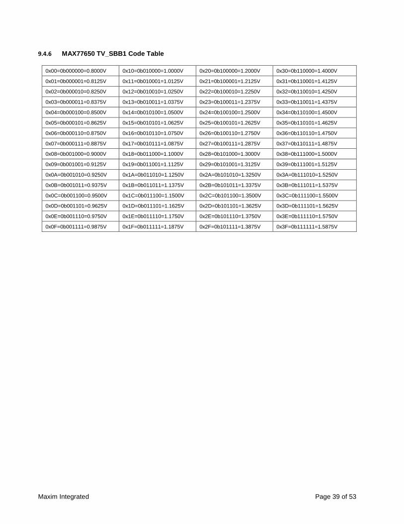
9.4.6 MAX77650 TV_SBB1 Code Table
0x00=0b000000=0.8000V 0x10=0b010000=1.0000V 0x20=0b100000=1.2000V 0x30=0b110000=1.4000V
0x01=0b000001=0.8125V 0x11=0b010001=1.0125V 0x21=0b100001=1.2125V 0x31=0b110001=1.4125V
0x02=0b000010=0.8250V 0x12=0b010010=1.0250V 0x22=0b100010=1.2250V 0x32=0b110010=1.4250V
0x03=0b000011=0.8375V 0x13=0b010011=1.0375V 0x23=0b100011=1.2375V 0x33=0b110011=1.4375V
0x04=0b000100=0.8500V 0x14=0b010100=1.0500V 0x24=0b100100=1.2500V 0x34=0b110100=1.4500V
0x05=0b000101=0.8625V 0x15=0b010101=1.0625V 0x25=0b100101=1.2625V 0x35=0b110101=1.4625V
0x06=0b000110=0.8750V 0x16=0b010110=1.0750V 0x26=0b100110=1.2750V 0x36=0b110110=1.4750V
0x07=0b000111=0.8875V 0x17=0b010111=1.0875V 0x27=0b100111=1.2875V 0x37=0b110111=1.4875V
0x08=0b001000=0.9000V 0x18=0b011000=1.1000V 0x28=0b101000=1.3000V 0x38=0b111000=1.5000V
0x09=0b001001=0.9125V 0x19=0b011001=1.1125V 0x29=0b101001=1.3125V 0x39=0b111001=1.5125V
0x0A=0b001010=0.9250V 0x1A=0b011010=1.1250V 0x2A=0b101010=1.3250V 0x3A=0b111010=1.5250V
0x0B=0b001011=0.9375V 0x1B=0b011011=1.1375V 0x2B=0b101011=1.3375V 0x3B=0b111011=1.5375V
0x0C=0b001100=0.9500V 0x1C=0b011100=1.1500V 0x2C=0b101100=1.3500V 0x3C=0b111100=1.5500V
0x0D=0b001101=0.9625V 0x1D=0b011101=1.1625V 0x2D=0b101101=1.3625V 0x3D=0b111101=1.5625V
0x0E=0b001110=0.9750V 0x1E=0b011110=1.1750V 0x2E=0b101110=1.3750V 0x3E=0b111110=1.5750V
0x0F=0b001111=0.9875V 0x1F=0b011111=1.1875V 0x2F=0b101111=1.3875V 0x3F=0b111111=1.5875V
Maxim Integrated Page 40 of 53
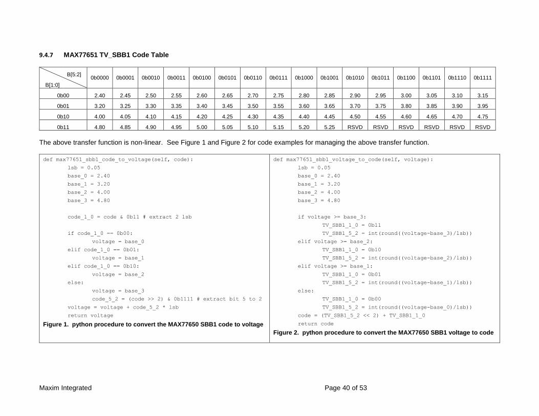
9.4.7 MAX77651 TV_SBB1 Code Table
B[5:2] 0b0000 0b0001 0b0010 0b0011 0b0100 0b0101 0b0110 0b0111 0b1000 0b1001 0b1010 0b1011 0b1100 0b1101 0b1110 0b1111
B[1:0]
0b00 2.40 2.45 2.50 2.55 2.60 2.65 2.70 2.75 2.80 2.85 2.90 2.95 3.00 3.05 3.10 3.15
0b01 3.20 3.25 3.30 3.35 3.40 3.45 3.50 3.55 3.60 3.65 3.70 3.75 3.80 3.85 3.90 3.95
0b10 4.00 4.05 4.10 4.15 4.20 4.25 4.30 4.35 4.40 4.45 4.50 4.55 4.60 4.65 4.70 4.75
0b11 4.80 4.85 4.90 4.95 5.00 5.05 5.10 5.15 5.20 5.25 RSVD RSVD RSVD RSVD RSVD RSVD
The above transfer function is non-linear. See Figure 1 and Figure 2 for code examples for managing the above transfer function.
def max77651_sbb1_code_to_voltage(self, code):
lsb = 0.05
base_0 = 2.40
base_1 = 3.20
base_2 = 4.00
base_3 = 4.80
code_1_0 = code & 0b11 # extract 2 lsb
if code_1_0 == 0b00:
voltage = base_0
elif code_1_0 == 0b01:
voltage = base_1
elif code_1_0 == 0b10:
voltage = base_2
else:
voltage = base_3
code_5_2 = (code >> 2) & 0b1111 # extract bit 5 to 2
voltage = voltage + code_5_2 * lsb
return voltage
Figure 1. python procedure to convert the MAX77650 SBB1 code to voltage
def max77651_sbb1_voltage_to_code(self, voltage):
lsb = 0.05
base_0 = 2.40
base_1 = 3.20
base_2 = 4.00
base_3 = 4.80
if voltage >= base_3:
TV_SBB1_1_0 = 0b11
TV_SBB1_5_2 = int(round((voltage-base_3)/lsb))
elif voltage >= base_2:
TV_SBB1_1_0 = 0b10
TV_SBB1_5_2 = int(round((voltage-base_2)/lsb))
elif voltage >= base_1:
TV_SBB1_1_0 = 0b01
TV_SBB1_5_2 = int(round((voltage-base_1)/lsb))
else:
TV_SBB1_1_0 = 0b00
TV_SBB1_5_2 = int(round((voltage-base_0)/lsb))
code = (TV_SBB1_5_2 << 2) + TV_SBB1_1_0
return code
Figure 2. python procedure to convert the MAX77650 SBB1 voltage to code

Maxim Integrated
9.4.8 CNFG_SBB1_B
Register Name CNFG_SBB1_B
I2C Slave Address function of ADDR OTP bit
Register Address 0x2C
Reset Value (HEX) OTP
Reset Value (BIN) 0b0000xxxx
Reset Condition SYSRST=1
Access Type R/W
Register Type Configuration
Bit Default Bit Name Description Reset Access Type
7 0 BLANK Blank. There is no bit at this location. Write to 0. Reads are don't care. SYSRST=1 R/W
6 0 BLANK Blank. There is no bit at this location. Write to 0. Reads are don't care. SYSRST=1 R/W
5 0 BLANK Blank. There is no bit at this location. Write to 0. Reads are don't care. SYSRST=1 R/W
4 0 BLANK Blank. There is no bit at this location. Write to 0. Reads are don't care. SYSRST=1 R/W
3 x ADE_SBB1
SIMO Buck-Boost Channel 1 Active-Discharge Enable 0=The active discharge function is disabled. When SBB1 is disabled, it's discharge rate is a function of the output capacitance and the external load. 1=The active discharge function is enabled. When SBB1 is disabled, an internal resistor (RAD_SBB1) is activated from SBB1 to PGND to help the output voltage discharge. The output voltage discharge rate is a function of the output capacitance, the external loading, and the internal RAD_SBB1 load.
SYSRST=1 R/W
2 x
EN_SBB1[2:0]
Enable Control for SIMO Buck-Boost Channel 1. 0b000 = SBB1 powers-up and powers-down in FPS slot 0 0b001 = SBB1 powers-up and powers-down in FPS slot 1 0b010 = SBB1 powers-up and powers-down in FPS slot 2 0b011 = SBB1 powers-up and powers-down in FPS slot 3 0b100 = SBB1 is off irrespective of FPS 0b101 = same as 0b100 0b110 = SBB1 is on irrespective of FPS whenever the on/off controller is in its "On via Software" or "On via On/Off Controller" states. 0b111 = same as 0b110 Prior to enabling the SIMO, program the bias circuits to normal power mode (SBIA_LPM=0). After the SIMO is enabled, the bias circuits may be programmed back to low power mode (SBIA_LPM=1) to decrease quiescent current.
SYSRST=1 R/W
1 x SYSRST=1 R/W
0 x SYSRST=1 R/W

Maxim Integrated
9.4.9 CNFG_SBB2_A
Register Name CNFG_SBB2_A
I2C Slave Address function of ADDR OTP bit
Register Address 0x2D
Reset Value (HEX) OTP
Reset Value (BIN) 0bxxxxxxxx
Reset Condition SYSRST=1
Access Type R/W
Register Type Configuration
Bit Default Bit Name Description Reset Access Type
7 x
IP_SBB2[1:0]
SIMO Buck-Boost Channel 1 Peak Current Limit 0b00=1.000A 0b01=0.866A 0b10=0.707A 0b11=0.500A
SYSRST=1 R/W
6 x SYSRST=1 R/W
5 x
TV_SBB2[5:0]
SIMO Buck-Boost Channel 2 Target Output Voltage This 6-bit configuration is a linear transfer function that starts at 0.8V, ends at 3.95V, with 50mV increments for the MAX77650. For the MAX77651, the transfer function starts ad 2.4V, ends at 3.95V, with 50mV increments. See the "TV_SBBx" tab in this spreadsheet for a complete table of values.
SYSRST=1 R/W
4 x SYSRST=1 R/W
3 x SYSRST=1 R/W
2 x SYSRST=1 R/W
1 x SYSRST=1 R/W
0 x SYSRST=1 R/W

Maxim Integrated
9.4.10 MAX77650 TV_SBB2 Code Table
0x00=0b000000=0.80V 0x10=0b010000=1.60V 0x20=0b100000=2.40V 0x30=0b110000=3.20V
0x01=0b000001=0.85V 0x11=0b010001=1.65V 0x21=0b100001=2.45V 0x31=0b110001=3.25V
0x02=0b000010=0.90V 0x12=0b010010=1.70V 0x22=0b100010=2.50V 0x32=0b110010=3.30V
0x03=0b000011=0.95V 0x13=0b010011=1.75V 0x23=0b100011=2.55V 0x33=0b110011=3.35V
0x04=0b000100=1.00V 0x14=0b010100=1.80V 0x24=0b100100=2.60V 0x34=0b110100=3.40V
0x05=0b000101=1.05V 0x15=0b010101=1.85V 0x25=0b100101=2.65V 0x35=0b110101=3.45V
0x06=0b000110=1.10V 0x16=0b010110=1.90V 0x26=0b100110=2.70V 0x36=0b110110=3.50V
0x07=0b000111=1.15V 0x17=0b010111=1.95V 0x27=0b100111=2.75V 0x37=0b110111=3.55V
0x08=0b001000=1.20V 0x18=0b011000=2.00V 0x28=0b101000=2.80V 0x38=0b111000=3.60V
0x09=0b001001=1.25V 0x19=0b011001=2.05V 0x29=0b101001=2.85V 0x39=0b111001=3.65V
0x0A=0b001010=1.30V 0x1A=0b011010=2.10V 0x2A=0b101010=2.90V 0x3A=0b111010=3.70V
0x0B=0b001011=1.35V 0x1B=0b011011=2.15V 0x2B=0b101011=2.95V 0x3B=0b111011=3.75V
0x0C=0b001100=1.40V 0x1C=0b011100=2.20V 0x2C=0b101100=3.00V 0x3C=0b111100=3.80V
0x0D=0b001101=1.45V 0x1D=0b011101=2.25V 0x2D=0b101101=3.05V 0x3D=0b111101=3.85V
0x0E=0b001110=1.50V 0x1E=0b011110=2.30V 0x2E=0b101110=3.10V 0x3E=0b111110=3.90V
0x0F=0b001111=1.55V 0x1F=0b011111=2.35V 0x2F=0b101111=3.15V 0x3F=0b111111=3.95V
9.4.11 MAX77651 TV_SBB2 Code Table
0x00=0b000000=2.40V 0x10=0b010000=3.20V 0x20=0b100000=4.00V 0x30=0b110000=4.80V
0x01=0b000001=2.45V 0x11=0b010001=3.25V 0x21=0b100001=4.05V 0x31=0b110001=4.85V
0x02=0b000010=2.50V 0x12=0b010010=3.30V 0x22=0b100010=4.10V 0x32=0b110010=4.90V
0x03=0b000011=2.55V 0x13=0b010011=3.35V 0x23=0b100011=4.15V 0x33=0b110011=4.95V
0x04=0b000100=2.60V 0x14=0b010100=3.40V 0x24=0b100100=4.20V 0x34=0b110100=5.00V
0x05=0b000101=2.65V 0x15=0b010101=3.45V 0x25=0b100101=4.25V 0x35=0b110101=5.05V
0x06=0b000110=2.70V 0x16=0b010110=3.50V 0x26=0b100110=4.30V 0x36=0b110110=5.10V
0x07=0b000111=2.75V 0x17=0b010111=3.55V 0x27=0b100111=4.35V 0x37=0b110111=5.15V
0x08=0b001000=2.80V 0x18=0b011000=3.60V 0x28=0b101000=4.40V 0x38=0b111000=5.20V
0x09=0b001001=2.85V 0x19=0b011001=3.65V 0x29=0b101001=4.45V 0x39=0b111001=5.25V
0x0A=0b001010=2.90V 0x1A=0b011010=3.70V 0x2A=0b101010=4.50V 0x3A=0b111010=RSVD
0x0B=0b001011=2.95V 0x1B=0b011011=3.75V 0x2B=0b101011=4.55V 0x3B=0b111011=RSVD
0x0C=0b001100=3.00V 0x1C=0b011100=3.80V 0x2C=0b101100=4.60V 0x3C=0b111100=RSVD
0x0D=0b001101=3.05V 0x1D=0b011101=3.85V 0x2D=0b101101=4.65V 0x3D=0b111101=RSVD
0x0E=0b001110=3.10V 0x1E=0b011110=3.90V 0x2E=0b101110=4.70V 0x3E=0b111110=RSVD
0x0F=0b001111=3.15V 0x1F=0b011111=3.95V 0x2F=0b101111=4.75V 0x3F=0b111111=RSVD

Maxim Integrated
9.4.12 CNFG_SBB2_B
Register Name CNFG_SBB2_B
I2C Slave Address function of ADDR OTP bit
Register Address 0x2E
Reset Value (HEX) OTP
Reset Value (BIN) 0b0000xxxx
Reset Condition SYSRST=1
Access Type R/W
Register Type Configuration
Bit Default Bit Name Description Reset Access Type
7 0 BLANK Blank. There is no bit at this location. Write to 0. Reads are don't care. SYSRST=1 R/W
6 0 BLANK Blank. There is no bit at this location. Write to 0. Reads are don't care. SYSRST=1 R/W
5 0 BLANK Blank. There is no bit at this location. Write to 0. Reads are don't care. SYSRST=1 R/W
4 0 BLANK Blank. There is no bit at this location. Write to 0. Reads are don't care. SYSRST=1 R/W
3 x ADE_SBB2
SIMO Buck-Boost Channel 2 Active-Discharge Enable 0=The active discharge function is disabled. When SBB2 is disabled, it's discharge rate is a function of the output capacitance and the external load. 1=The active discharge function is enabled. When SBB2 is disabled, an internal resistor (RAD_SBB2) is activated from SBB2 to PGND to help the output voltage discharge. The output voltage discharge rate is a function of the output capacitance, the external loading, and the internal RAD_SBB2 load.
SYSRST=1 R/W
2 x
EN_SBB2[2:0]
Enable Control for SIMO Buck-Boost Channel 2. 0b000 = SBB2 powers-up and powers-down in FPS slot 0 0b001 = SBB2 powers-up and powers-down in FPS slot 1 0b010 = SBB2 powers-up and powers-down in FPS slot 2 0b011 = SBB2 powers-up and powers-down in FPS slot 3 0b100 = SBB2 is off irrespective of FPS 0b101 = same as 0b100 0b110 = SBB2 is on irrespective of FPS whenever the on/off controller is in its "On via Software" or "On via On/Off Controller" states. 0b111 = same as 0b110 Prior to enabling the SIMO, program the bias circuits to normal power mode (SBIA_LPM=0). After the SIMO is enabled, the bias circuits may be programmed back to low power mode (SBIA_LPM=1) to decrease quiescent current.
SYSRST=1 R/W
1 x SYSRST=1 R/W
0 x SYSRST=1 R/W
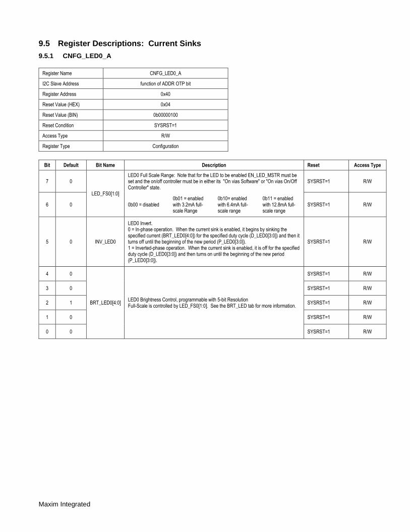
Maxim Integrated
9.5 Register Descriptions: Current Sinks
9.5.1 CNFG_LED0_A
Register Name CNFG_LED0_A
I2C Slave Address function of ADDR OTP bit
Register Address 0x40
Reset Value (HEX) 0x04
Reset Value (BIN) 0b00000100
Reset Condition SYSRST=1
Access Type R/W
Register Type Configuration
Bit Default Bit Name Description Reset Access Type
7 0
LED_FS0[1:0]
LED0 Full Scale Range: Note that for the LED to be enabled EN_LED_MSTR must be set and the on/off controller must be in either its "On vias Software" or "On vias On/Off Controller" state.
SYSRST=1 R/W
6 0 0b00 = disabled 0b01 = enabled with 3.2mA full-scale Range
0b10= enabled with 6.4mA full-scale range
0b11 = enabled with 12.8mA full-scale range
SYSRST=1 R/W
5 0 INV_LED0
LED0 Invert. 0 = In-phase operation. When the current sink is enabled, it begins by sinking the specified current (BRT_LED0[4:0]) for the specified duty cycle (D_LED0[3:0]) and then it turns off until the beginning of the new period (P_LED0[3:0]). 1 = Inverted-phase operation. When the current sink is enabled, it is off for the specified duty cycle (D_LED0[3:0]) and then turns on until the beginning of the new period (P_LED0[3:0]).
SYSRST=1 R/W
4 0
BRT_LED0[4:0] LED0 Brightness Control, programmable with 5-bit Resolution Full-Scale is controlled by LED_FS0[1:0]. See the BRT_LED tab for more information.
SYSRST=1 R/W
3 0 SYSRST=1 R/W
2 1 SYSRST=1 R/W
1 0 SYSRST=1 R/W
0 0 SYSRST=1 R/W

Maxim Integrated
9.5.2 CNFG_LED0_B
Register Name CNFG_LED0_B
I2C Slave Address function of ADDR OTP bit
Register Address 0x43
Reset Value (HEX) 0x0F
Reset Value (BIN) 0b00001111
Reset Condition SYSRST=1
Access Type R/W
Register Type Configuration
Bit Default Bit Name Description Reset Access Type
7 0
P_LED0[3:0]
LED0 Period Settings SYSRST=1 R/W
6 0 0b0000 = 0.5s 0b0001 = 1.0s 0b0010 = 1.5s 0b0011 = 2.0s
0b0100 = 2.5s 0b0101 = 3.0s 0b0110 = 3.5s 0b0111 = 4.0s
0b1000 = 4.5s 0b1001 = 5.0s 0b1010 = 5.5s 0b1011 = 6.0s
0b1100 = 6.5s 0b1101 = 7s 0b1110 = 7.5s 0b1111 = 8s
SYSRST=1 R/W
5 0 SYSRST=1 R/W
4 0 SYSRST=1 R/W
3 1
D_LED0[3:0]
LED0 On Duty-Cycle Settings SYSRST=1 R/W
2 1 0b0000 = 6.25% 0b0001 = 12.5% 0b0010 = 18.75% 0b0011 = 25%
0b0100 = 31.25% 0b0101 = 37.5% 0b0110 = 43.75% 0b0111 = 50%
0b1000 = 56.25% 0b1001 = 62.5% 0b1010 = 68.75% 0b1011 = 75%
0b1100 = 81.25% 0b1101 = 87.5% 0b1110 = 93.75% 0b1111 = 100%
SYSRST=1 R/W
1 1 SYSRST=1 R/W
0 1 SYSRST=1 R/W

Maxim Integrated
9.5.3 CNFG_LED1_A
Register Name CNFG_LED1_A
I2C Slave Address function of ADDR OTP bit
Register Address 0x41
Reset Value (HEX) 0x04
Reset Value (BIN) 0b00000100
Reset Condition SYSRST=1
Access Type R/W
Register Type Configuration
Bit Default Bit Name Description Reset Access Type
7 0
LED_FS1[1:0]
LED1 Full Scale Range: Note that for the LED to be enabled EN_LED_MSTR must be set and the on/off controller must be in either its "On vias Software" or "On vias On/Off Controller" state.
SYSRST=1 R/W
6 0 0b00 = disabled 0b01 = enabled with 3.2mA full-scale Range
0b10= enabled with 6.4mA full-scale range
0b11 = enabled with 12.8mA full-scale range
SYSRST=1 R/W
5 0 INV_LED1
LED1 Invert. 0 = In-phase operation. When the current sink is enabled, it begins by sinking the specified current (BRT_LED1[4:0]) for the specified duty cycle (D_LED1[3:0]) and then it turns off until the beginning of the new period (P_LED1[3:0]). 1 = Inverted-phase operation. When the current sink is enabled, it is off for the specified duty cycle (D_LED1[3:0]) and then turns on until the beginning of the new period (P_LED1[3:0]).
SYSRST=1 R/W
4 0
BRT_LED1[4:0] LED1 Brightness Control, programmable with 5-bit Resolution Full-Scale is controlled by LED_FS1[1:0]. See the BRT_LED tab for more information.
SYSRST=1 R/W
3 0 SYSRST=1 R/W
2 1 SYSRST=1 R/W
1 0 SYSRST=1 R/W
0 0 SYSRST=1 R/W

Maxim Integrated
9.5.4 CNFG_LED1_B
Register Name CNFG_LED1_B
I2C Slave Address function of ADDR OTP bit
Register Address 0x44
Reset Value (HEX) 0x0F
Reset Value (BIN) 0b00001111
Reset Condition SYSRST=1
Access Type R/W
Register Type Configuration
Bit Default Bit Name Description Reset Access Type
7 0
P_LED1[3:0]
LED1 Period Settings SYSRST=1 R/W
6 0 0b0000 = 0.5s 0b0001 = 1.0s 0b0010 = 1.5s 0b0011 = 2.0s
0b0100 = 2.5s 0b0101 = 3.0s 0b0110 = 3.5s 0b0111 = 4.0s
0b1000 = 4.5s 0b1001 = 5.0s 0b1010 = 5.5s 0b1011 = 6.0s
0b1100 = 6.5s 0b1101 = 7s 0b1110 = 7.5s 0b1111 = 8s
SYSRST=1 R/W
5 0 SYSRST=1 R/W
4 0 SYSRST=1 R/W
3 1
D_LED1[3:0]
LED1 On Duty-Cycle Settings SYSRST=1 R/W
2 1 0b0000 = 6.25% 0b0001 = 12.5% 0b0010 = 18.75% 0b0011 = 25%
0b0100 = 31.25% 0b0101 = 37.5% 0b0110 = 43.75% 0b0111 = 50%
0b1000 = 56.25% 0b1001 = 62.5% 0b1010 = 68.75% 0b1011 = 75%
0b1100 = 81.25% 0b1101 = 87.5% 0b1110 = 93.75% 0b1111 = 100%
SYSRST=1 R/W
1 1 SYSRST=1 R/W
0 1 SYSRST=1 R/W

Maxim Integrated
9.5.5 CNFG_LED2_A
Register Name CNFG_LED2_A
I2C Slave Address function of ADDR OTP bit
Register Address 0x42
Reset Value (HEX) 0x04
Reset Value (BIN) 0b00000100
Reset Condition SYSRST=1
Access Type R/W
Register Type Configuration
Bit Default Bit Name Description Reset Access Type
7 0
LED_FS2[1:0]
LED2 Full-Scale Range: Note that for the LED to be enabled EN_LED_MSTR must be set and the on/off controller must be in either its "On vias Software" or "On vias On/Off Controller" state.
SYSRST=1 R/W
6 0 0b00 = disabled 0b01 = enabled with 3.2mA full-scale Range
0b10= enabled with 6.4mA full-scale range
0b11 = enabled with 12.8mA full-scale range
SYSRST=1 R/W
5 0 INV_LED2
LED2 Invert. 0 = In-phase operation. When the current sink is enabled, it begins by sinking the specified current (BRT_LED2[4:0]) for the specified duty cycle (D_LED2[3:0]) and then it turns off until the beginning of the new period (P_LED2[3:0]). 1 = Inverted-phase operation. When the current sink is enabled, it is off for the specified duty cycle (D_LED2[3:0]) and then turns on until the beginning of the new period (P_LED2[3:0]).
SYSRST=1 R/W
4 0
BRT_LED2[4:0] LED2 Brightness Control, programmable with 5-bit Resolution Full-Scale is controlled by LED_FS2[1:0]. See the BRT_LED tab for more information.
SYSRST=1 R/W
3 0 SYSRST=1 R/W
2 1 SYSRST=1 R/W
1 0 SYSRST=1 R/W
0 0 SYSRST=1 R/W

Maxim Integrated
9.5.6 CNFG_LED2_B
Register Name CNFG_LED0_B
I2C Slave Address function of ADDR OTP bit
Register Address 0x43
Reset Value (HEX) 0x0F
Reset Value (BIN) 0b00001111
Reset Condition SYSRST=1
Access Type R/W
Register Type Configuration
Bit Default Bit Name Description Reset Access Type
7 0
P_LED2[3:0]
LED2 Period Settings SYSRST=1 R/W
6 0 0b0000 = 0.5s 0b0001 = 1.0s 0b0010 = 1.5s 0b0011 = 2.0s
0b0100 = 2.5s 0b0101 = 3.0s 0b0110 = 3.5s 0b0111 = 4.0s
0b1000 = 4.5s 0b1001 = 5.0s 0b1010 = 5.5s 0b1011 = 6.0s
0b1100 = 6.5s 0b1101 = 7s 0b1110 = 7.5s 0b1111 = 8s
SYSRST=1 R/W
5 0 SYSRST=1 R/W
4 0 SYSRST=1 R/W
3 1
D_LED2[3:0]
LED2 On Duty-Cycle Settings SYSRST=1 R/W
2 1 0b0000 = 6.25% 0b0001 = 12.5% 0b0010 = 18.75% 0b0011 = 25%
0b0100 = 31.25% 0b0101 = 37.5% 0b0110 = 43.75% 0b0111 = 50%
0b1000 = 56.25% 0b1001 = 62.5% 0b1010 = 68.75% 0b1011 = 75%
0b1100 = 81.25% 0b1101 = 87.5% 0b1110 = 93.75% 0b1111 = 100%
SYSRST=1 R/W
1 1 SYSRST=1 R/W
0 1 SYSRST=1 R/W

Maxim Integrated
9.5.7 CNFG_LED_TOP
Register Name CNFG_LED_TOP
I2C Slave Address function of ADDR OTP bit
Register Address 0x46
Reset Value (HEX) 0x0D
Reset Value (BIN) 0b00001101
Reset Condition SYSRST=1
Access Type Mixed
Register Type Configuration
Bit Default Bit Name Description Reset Access Type
7 0 RESERVED Reserved. Unutilized bit. Write to 0. Reads are don't care. SYSRST=1 R/W
6 0 RESERVED Reserved. Unutilized bit. Write to 0. Reads are don't care. SYSRST=1 R/W
5 0 RESERVED Reserved. Unutilized bit. Write to 0. Reads are don't care. SYSRST=1 R/W
4 0 RESERVED Reserved. Unutilized bit. Write to 0. Reads are don't care. SYSRST=1 R/W
3 1 RESERVED Reserved. Unutilized bit. Write to 0. Reads are don't care. SYSRST=1 R/W
2 1 RESERVED Reserved. Unutilized bit. Write to 0. Reads are don't care. SYSRST=1 R/W
1 0 CLK_64_S
64Hz Clock Status. CLK_64_S is internally driven by the same clock that drives the current sink PWM logic. CLK_64_S is provided to allow software to align its timing with that of the internal PWM logic when setting up custom LED blink patterns. CLK_64_S has a 10% duty cycle. 0= The 64Hz root clock is logic low. 1 = The 64Hz root clock is logic high.
SYSRST=1 R
0 1 EN_LED_MSTR
Master LED Enable Bit 0= The current sinks are disabled. 1 = The current sinks are enabled if their individual enable it is enabled (EN_LEDx) and the on/off controller is in its "On via Software" or "On via On/Off Controller" states.
SYSRST=1 R/W
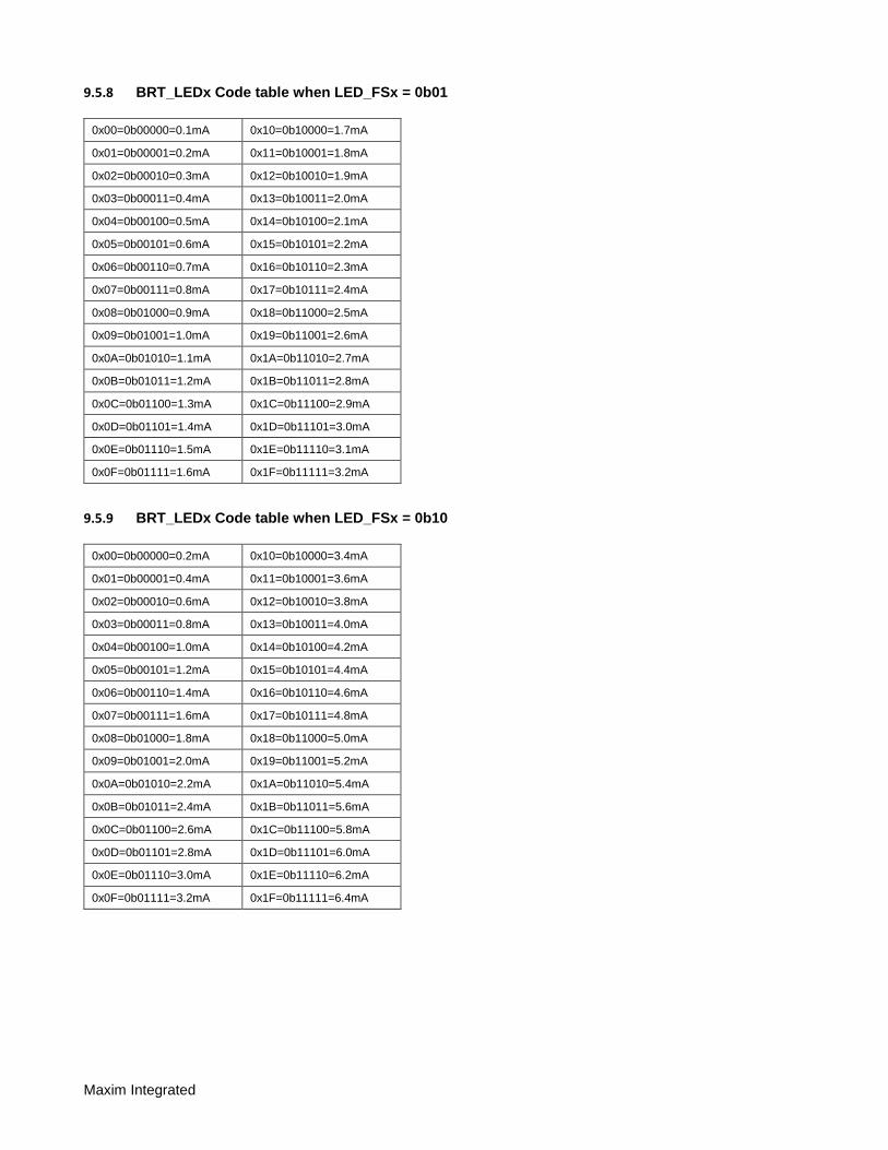
Maxim Integrated
9.5.8 BRT_LEDx Code table when LED_FSx = 0b01
0x00=0b00000=0.1mA 0x10=0b10000=1.7mA
0x01=0b00001=0.2mA 0x11=0b10001=1.8mA
0x02=0b00010=0.3mA 0x12=0b10010=1.9mA
0x03=0b00011=0.4mA 0x13=0b10011=2.0mA
0x04=0b00100=0.5mA 0x14=0b10100=2.1mA
0x05=0b00101=0.6mA 0x15=0b10101=2.2mA
0x06=0b00110=0.7mA 0x16=0b10110=2.3mA
0x07=0b00111=0.8mA 0x17=0b10111=2.4mA
0x08=0b01000=0.9mA 0x18=0b11000=2.5mA
0x09=0b01001=1.0mA 0x19=0b11001=2.6mA
0x0A=0b01010=1.1mA 0x1A=0b11010=2.7mA
0x0B=0b01011=1.2mA 0x1B=0b11011=2.8mA
0x0C=0b01100=1.3mA 0x1C=0b11100=2.9mA
0x0D=0b01101=1.4mA 0x1D=0b11101=3.0mA
0x0E=0b01110=1.5mA 0x1E=0b11110=3.1mA
0x0F=0b01111=1.6mA 0x1F=0b11111=3.2mA
9.5.9 BRT_LEDx Code table when LED_FSx = 0b10
0x00=0b00000=0.2mA 0x10=0b10000=3.4mA
0x01=0b00001=0.4mA 0x11=0b10001=3.6mA
0x02=0b00010=0.6mA 0x12=0b10010=3.8mA
0x03=0b00011=0.8mA 0x13=0b10011=4.0mA
0x04=0b00100=1.0mA 0x14=0b10100=4.2mA
0x05=0b00101=1.2mA 0x15=0b10101=4.4mA
0x06=0b00110=1.4mA 0x16=0b10110=4.6mA
0x07=0b00111=1.6mA 0x17=0b10111=4.8mA
0x08=0b01000=1.8mA 0x18=0b11000=5.0mA
0x09=0b01001=2.0mA 0x19=0b11001=5.2mA
0x0A=0b01010=2.2mA 0x1A=0b11010=5.4mA
0x0B=0b01011=2.4mA 0x1B=0b11011=5.6mA
0x0C=0b01100=2.6mA 0x1C=0b11100=5.8mA
0x0D=0b01101=2.8mA 0x1D=0b11101=6.0mA
0x0E=0b01110=3.0mA 0x1E=0b11110=6.2mA
0x0F=0b01111=3.2mA 0x1F=0b11111=6.4mA

Maxim Integrated
9.5.10 BRT_LEDx Code table when LED_FSx = 0b11
0x00=0b00000=0.4mA 0x10=0b10000=6.8mA
0x01=0b00001=0.8mA 0x11=0b10001=7.2mA
0x02=0b00010=1.2mA 0x12=0b10010=7.6mA
0x03=0b00011=1.6mA 0x13=0b10011=8.0mA
0x04=0b00100=2.0mA 0x14=0b10100=8.4mA
0x05=0b00101=2.4mA 0x15=0b10101=8.8mA
0x06=0b00110=2.8mA 0x16=0b10110=9.2mA
0x07=0b00111=3.2mA 0x17=0b10111=9.6mA
0x08=0b01000=3.6mA 0x18=0b11000=10.0mA
0x09=0b01001=4.0mA 0x19=0b11001=10.4mA
0x0A=0b01010=4.4mA 0x1A=0b11010=10.8mA
0x0B=0b01011=4.8mA 0x1B=0b11011=11.2mA
0x0C=0b01100=5.2mA 0x1C=0b11100=11.6mA
0x0D=0b01101=5.6mA 0x1D=0b11101=12.0mA
0x0E=0b01110=6.0mA 0x1E=0b11110=12.4mA
0x0F=0b01111=6.4mA 0x1F=0b11111=12.8mA
10 Revision History The following changes were made in preliminary versions prior to initial release of this user guide.
1. Added the Contents section and improved the heading structure within the document enhancing navigation ability.
2. Added the Register Reset Conditions section 3. Added the Software Management of the Charger section 4. Added the Managing SIMO Current Limits section 5. Added the Managing Main-Bias Circuits (SBIA) section 6. Enhanced the Changing Regulator Output Voltages section 7. SBIA_LPM was changed to an OTP option 8. DBEN_nEN was changed to an OTP option 9. Added the Managing VSYS_REG, CHG_CV, CHG_CV_JEITA section 10. Changed CNFG_SBB_TOP register contents 11. Added Quick Reference File section 12. In the Managing Main-Bias Circuits (SBIA_LPM) section, updated step 1 to say SBIA_LPM = 0 (was
SBIA_LPM = 1). Updated step 2 to say SBIA_LPM = 1 (was SBIA_LPM = 0). These were typos. 13. In the CNFG_CHG_X register, changed the description for ICHGIN_LIM[2:0] to reflect the
ICHGIN_LIM_DEF OTP. 14. Updated the MAX77651 TV_SBB1 Code Table and the MAX77651 TV_SBB2 Code Table to reflect that
output voltages above 5.25V are now reserved.

Maxim Integrated
©2017 by Maxim Integrated Products, Inc. All rights reserved. Information in this publication concerning the devices, applications, or technology described is intended to suggest possible uses and may be superseded. MAXIM INTEGRATED PRODUCTS, INC. DOES NOT ASSUME LIABILITY FOR OR PROVIDE A REPRESENTATION OF ACCURACY OF THE INFORMATION, DEVICES, OR TECHNOLOGY DESCRIBED IN THIS DOCUMENT. MAXIM ALSO DOES NOT ASSUME LIABILITY FOR INTELLECTUAL PROPERTY INFRINGEMENT RELATED IN ANY MANNER TO USE OF INFORMATION, DEVICES, OR TECHNOLOGY DESCRIBED HEREIN OR OTHERWISE. The information contained within this document has been verified according to the general principles of electrical and mechanical engineering or registered trademarks of Maxim Integrated Products, Inc. All other product or service names are the property of their respective owners.