max9880a evaluation kit - maxim integrated · max9880a evaluation kit evaluates: max9880a for...
TRANSCRIPT
_______________________________________________________________ Maxim Integrated Products 1
MAX9880A Evaluation Kit
Eva
lua
tes: M
AX
98
80
A
For pricing, delivery, and ordering information, please contact Maxim Direct at 1-888-629-4642, or visit Maxim’s website at www.maxim-ic.com.
General DescriptionThe MAX9880A evaluation kit (EV kit) is a fully assem-bled and tested surface-mount PCB that evaluates the MAX9880A IC, which is a low-power, high-performance, stereo audio codec with audio processing. To facilitate evaluation, the EV kit includes input and output RCA connections, capless and single-ended headphone con-nectors (J3, J4), and two on-board digital microphones (U15, U16).
Integrated into the EV kit design is a digital audio trans-ceiver (U11) and a USB stereo audio DAC (U12). The digital audio transceiver provides audio input and output through the on-board TOSLINK connectors (J5, J6) and the USB stereo audio DAC provides audio input through the mini-USB connector (J10).
The device’s I2C/2-wire and SPIK control bus are inter-faced to the on-board MAXQ2000 microcontroller, allow-ing for evaluation with the EV kit software.
FeaturesS USB Powered
S Configurable I2C/2-Wire or SPI Interface
S USB, TOSLINK, and RCA Audio Input Connections
S 3.5mm, TOSLINK, and RCA Audio Output Connections
S Windows® 2000-, Windows XP®-, and Windows Vista® (32-Bit)-Compatible Software
S Surface-Mount Components
S Proven PCB Layout
S Fully Assembled and Tested
Ordering Information
Component List
19-5325; Rev 1; 5/11
#Denotes RoHS compliant.
SPI is a trademark of Motorola, Inc.Windows, Windows XP, and Windows Vista are registered trademarks of Microsoft Corp.
PART TYPE
MAX9880AEVKIT# EV Kit
DESIGNATION QTY DESCRIPTION
CLK, DATA 0Not installed, miniature test points
C1–C9, C12–C17, C23–C26, C33, C43, C50, C53, C54, C67,
C68, C71, C77–C86, C92,
C93
391FF Q10%, 10V X5R ceramic capacitors (0402)Murata GRM155R61A105K
C10 1
2.2FF Q20%, 6.3V X5R ceramic capacitor (0402)Murata GRM155R60J225MTaiyo Yuden JMK105BJ225MV-F
C11, C18 2220FF Q20%, 4V tantalum capacitors (S case)Nichicon F950G227MSAAM1Q2
C19, C20, C31, C32, C57
50.01FF Q10%, 25V X7R ceramic capacitors (0402)Murata GRM155R71E103K
DESIGNATION QTY DESCRIPTION
C21, C22, C27, C29, C35, C40, C42, C44–C47, C51, C55, C56, C69, C75, C76
170.1FF Q10%, 6.3V X5R ceramic capacitors (0402)Murata GRM155R60J104K
C28 1
4700pF Q10%, 25V X7R ceramic capacitor (0603)Murata GRM188R71E473KTDK C1608X7R1E473K
C30 1
0.47FF Q10%, 6.3V X5R ceramic capacitor (0603)Murata GRM188R60J474KTDK C1608X5R0J474K
C34, C36, C37, C41, C73, C74
6
8pF Q0.5pF, 50V C0G ceramic capacitors (0402)Murata GRM1555C1H8R0DTaiyo Yuden UMK105CH080DV
C38, C58–C65, C87–C90
0Not installed, ceramic capacitors (0402)
MAX9880A Evaluation Kit
Eva
lua
tes:
M
AX
98
80
A
2 ______________________________________________________________________________________
Component List (continued)
UCSP is a trademark of Maxim Integrated Products, Inc.
DESIGNATION QTY DESCRIPTION
C39 133000pF Q10%, 16V X7Rceramic capacitor (0603)Murata GRM188R71C333K
C48, C49 2
18pF Q5%, 50V C0G ceramic capacitors (0603)Murata GRM1885C1H180JTDK C1608C0G1H180J
C52, C70, C91 310FF Q10%, 6.3V X5R ceramic capacitors (0805)Murata GRM219R60J106K
C66, C72 247FF Q20%, 6.3V tantalum capacitors (0805)AVX TLJR476M006R3200
D1 1 Yellow LED (0603)
D2 1 Red LED (0603)
FB1, FB2 2 0I resistors (0603)
J1, J9 2Phono jacks (side-entry PCB mount), white
J2, J8 2Phono jacks (side-entry PCB mount), red
J3 14-conductor, 3.5mm stereo headphone jack
J4 1 3.5mm stereo headphone jack
J5 1Fiber optic transmitting moduleToshiba TOTX147AL
J6 1Fiber optic receiving moduleToshiba TORX147L
J7, J10 2 Mini-USB type-B connectors
JU1–JU11, JU14–JU18, JU21, JU22, JU24, JU25, JU26, JU28,
JU29
23 2-pin headers, 0.1in centers
JU12 1 5-pin header, 0.1in centers
JU13, JU19, JU27
3 3 x 4-pin headers, 0.1in centers
JU20 1 3 x 2-pin header, 0.1in centers
JU23, JU30 0Not installed, 3-pin headers, 0.1in centers
DESIGNATION QTY DESCRIPTION
L1 147FH inductorMurata LQH43MN470J03L
R1–R4, R27 5 2.2kI Q1% resistors (0402)
R5, R6, R8, R28, R39
5 10kI Q5% resistors (0402)
R7, R15, R16, R29, R45–R48
0 Not installed, resistors (0402)
R9–R14, R30–R33, R41–R44
14 0I resistors (0402)
R17 1 402I Q1% resistor (0603)
R18 1 47kI Q5% resistor (0603)
R19, R20 2 220I Q5% resistors (0603)
R21, R22, R23 3 1.5kI Q5% resistors (0603)
R24, R25 2 27I Q5% resistors (0603)
R26 1 470I Q5% resistor (0603)
R34, R37 2 1.5kI Q5% resistors (0402)
R35, R36 2 22I Q5% resistors (0402)
R38 1 1MI Q5% resistor (0402)
TP1–TP5 5 Miniature test points
U1 1Audio codec (48 WLP)Maxim MAX9880AEWM+
U2, U3 0Not installed, SPDM left-input Class D amplifiers (9 WLP)
U4 1Bidirectional 4-channel level translator (12 UCSPK)Maxim MAX13042EEBC+
U5 1Microcontroller (56 TQFN-EP)Maxim MAXQ2000-RBX+
U6, U7 2
3.3V low-noise linear regulators(5 SC70)Maxim MAX8511EXK33+(Top Mark: AEI)
U8, U9 2
1.8V low-noise linear regulators(5 SC70)Maxim MAX8510EXK18+(Top Mark: AEA)
MAX9880A Evaluation Kit
Eva
lua
tes: M
AX
98
80
A
_______________________________________________________________________________________ 3
Component List (continued)
Component Suppliers
Note: Indicate that you are using the MAX9880A when contacting these component suppliers.
µMAX is a registered trademark of Maxim Integrated Products, Inc.
SUPPLIER PHONE WEBSITE
AVX Corporation 843-946-0238 www.avx.com
Murata Electronics North America, Inc. 770-436-1300 www.murata-northamerica.com
Nichicon USA 858-824-1515 www.nichicon-us.com
Taiyo Yuden 800-348-2496 www.t-yuden.com
TDK Corp. 847-803-6100 www.component.tdk.com
Toshiba America Electronic Components, Inc. 949-623-2900 www.toshiba.com/taec
DESIGNATION QTY DESCRIPTION
U10 1
2.5V low-noise linear regulator(5 SC70)Maxim MAX8511EXK25+(Top Mark: ADV)
U11 1Digital audio transceiver(28 SO)Cirrus CS8427-CSZ
U12 1USB audio codec (32 QFP)Texas Instruments PCM2707PJT
U13 1USB-to-UART converter (32 QFN)FTDI FT232BQ
U14 1EEPROM (8 SO)Atmel AT93C46EN-SH-B
U15, U16 2 1.8V digital microphones (6 LGA)
U17 1Logic-level translator(10-pin FMAXM)Maxim MAX1840EUB+
DESIGNATION QTY DESCRIPTION
Y1 1
12.288MHz crystal(3.2mm x 2.5mm)Kyocera CX3225SB12288D0FLJZ1
Y2 113MHz crystal oscillator(2.5mm x 2mm)ECS Inc. ECS-2033-130-BN
Y3 116MHz crystal oscillator(3.2mm x 2.5mm)
Y4 112MHz crystal oscillator(3.2mm x 2.5mm)
Y5 1 6MHz crystal
— 38 Shunts
— 1PCB: MAX9880A EVALUATION KIT
MAX9880A Evaluation Kit
Eva
lua
tes:
M
AX
98
80
A
4 ______________________________________________________________________________________
Quick StartRequired Equipment
• MAX9880A EV kit (USB cable included)
• Audio source with mini-USB connection
• Headphones and/or a speaker
• Windows 2000, Windows XP, or Windows Vista PC with a spare USB port
Note: In the following sections, software-related items are identified by bolding. Text in bold refers to items directly from the EV kit software. Text in bold and under-lined refers to items from the Windows operating system.
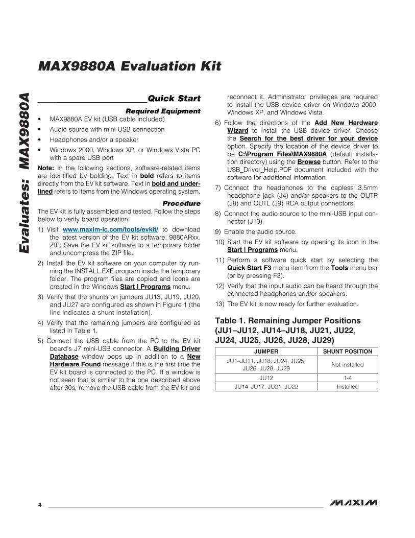
ProcedureThe EV kit is fully assembled and tested. Follow the steps below to verify board operation:
1) Visit www.maxim-ic.com/tools/evkit/ to download the latest version of the EV kit software, 9880ARxx.ZIP. Save the EV kit software to a temporary folder and uncompress the ZIP file.
2) Install the EV kit software on your computer by run-ning the INSTALL.EXE program inside the temporary folder. The program files are copied and icons are created in the Windows Start | Programs menu.
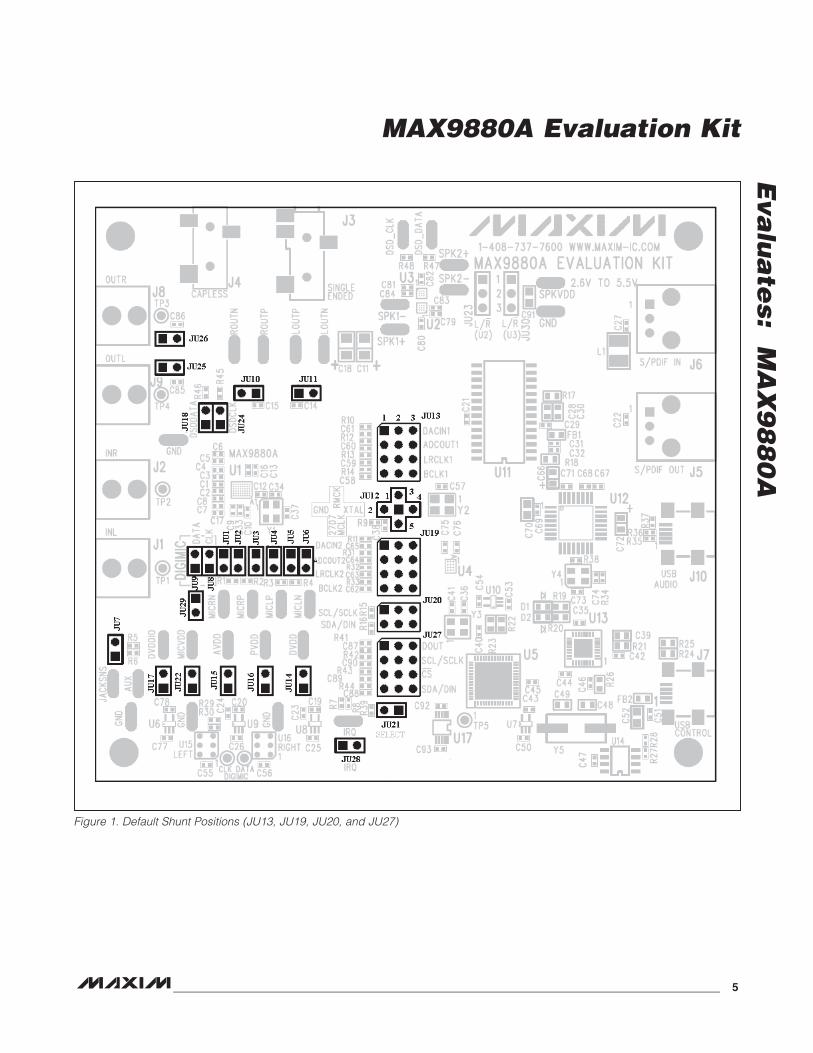
3) Verify that the shunts on jumpers JU13, JU19, JU20, and JU27 are configured as shown in Figure 1 (the line indicates a shunt installation).
4) Verify that the remaining jumpers are configured as listed in Table 1.
5) Connect the USB cable from the PC to the EV kit board’s J7 mini-USB connector. A Building Driver Database window pops up in addition to a New Hardware Found message if this is the first time the EV kit board is connected to the PC. If a window is not seen that is similar to the one described above after 30s, remove the USB cable from the EV kit and
reconnect it. Administrator privileges are required to install the USB device driver on Windows 2000, Windows XP, and Windows Vista.
6) Follow the directions of the Add New Hardware Wizard to install the USB device driver. Choose the Search for the best driver for your device option. Specify the location of the device driver to be C:\Program Files\MAX9880A (default installa-tion directory) using the Browse button. Refer to the USB_Driver_Help.PDF document included with the software for additional information.
7) Connect the headphones to the capless 3.5mm headphone jack (J4) and/or speakers to the OUTR (J8) and OUTL (J9) RCA output connectors.
8) Connect the audio source to the mini-USB input con-nector (J10).
9) Enable the audio source.
10) Start the EV kit software by opening its icon in the Start | Programs menu.
11) Perform a software quick start by selecting the Quick Start F3 menu item from the Tools menu bar (or by pressing F3).
12) Verify that the input audio can be heard through the connected headphones and/or speakers.
13) The EV kit is now ready for further evaluation.
Table 1. Remaining Jumper Positions (JU1–JU12, JU14–JU18, JU21, JU22, JU24, JU25, JU26, JU28, JU29)
JUMPER SHUNT POSITION
JU1–JU11, JU18, JU24, JU25, JU26, JU28, JU29
Not installed
JU12 1-4
JU14–JU17, JU21, JU22 Installed
MAX9880A Evaluation Kit
Eva
lua
tes: M
AX
98
80
A
_______________________________________________________________________________________ 5
Figure 1. Default Shunt Positions (JU13, JU19, JU20, and JU27)
MAX9880A Evaluation Kit
Eva
lua
tes:
M
AX
98
80
A
6 ______________________________________________________________________________________
Detailed Description of SoftwareThe MAX9880A EV kit software is divided into three tabs: Analog Audio, Digital Audio, and Control Registers. The analog and digital tabs are image-based tabs, pro-viding a visualization of the MAX9880A’s (U1) configura-tion and an interpretation of the register organization. The control tab provides a map of the device registers, as well as configuration control of each register bit.
The software also includes a Status group box (see the Status Register section), five command buttons, a menu bar, and a status bar. The status bar is used to report EV kit connectivity, the interface mode, the device’s address
(I2C mode), and the device’s revision ID. The functional-ity of the command buttons is provided in Table 2 and the menu bar items are discussed in the Menu Bar sec-tion.
The controls for the device registers are discussed in subsequent sections, which have been organized in the same manner as the register descriptions in the MAX9880A IC data sheet. As such, when evaluating the EV kit hardware and software, both the IC data sheet and the EV kit data sheet should be referenced.
Menu BarThe software’s menu bar provides five drop-down menus: File, View, Options, Tools, and Help. Their associated menu items are listed and detailed in Table 3.
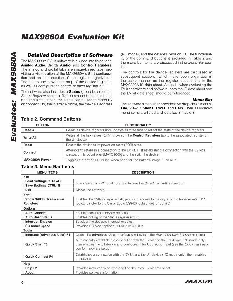
Table 2. Command Buttons
Table 3. Menu Bar Items
BUTTON FUNCTIONALITY
Read All Reads all device registers and updates all three tabs to reflect the state of the device registers.
Write AllWrites all the hex values (0x??) shown on the Control Registers tab to the associated register on the U1 device.
Reset Resets the device to its power-on-reset (POR) state.
ConnectAttempts to establish a connection to the EV kit. First establishing a connection with the EV kit’s on-board microcontroller (MAXQ2000) and then with the device.
MAX9880A Power Toggles the device SHDN bit. When enabled, the button’s image turns blue.
MENU ITEMS DESCRIPTIONFile| Load Settings CTRL+O
Loads/saves a .ax27 configuration file (see the Save/Load Settings section).| Save Settings CTRL+S| Exit Closes the software.View
| Show S/PDIF Transceiver Registers
Enables the CS8427 register tab, providing access to the digital audio transceiver’s (U11) registers (refer to the Cirrus Logic CS8427 data sheet for details).
Options| Auto Connect Enables continuous device detection.| Auto Read Status Enables polling of the Status register (0x00).| Interrupt Enables Set/clear the device’s interrupt enables.| I2C Clock Speed Provides I2C clock options: 100kHz or 400kHz.Tools| Interface (Advanced User) F1 Opens the Advanced User Interface window (see the Advanced User Interface section).
| Quick Start F3Automatically establishes a connection with the EV kit and the U1 device (I2C mode only), then enables the U1 device and configures it for USB audio input (see the Quick Start sec-tion for hardware setup).
| Quick Connect F4Establishes a connection with the EV kit and the U1 device (I2C mode only), then enables the device.
Help| Help F2 Provides instructions on where to find the latest EV kit data sheet.| About Provides software information.
MAX9880A Evaluation Kit
Eva
lua
tes: M
AX
98
80
A
_______________________________________________________________________________________ 7
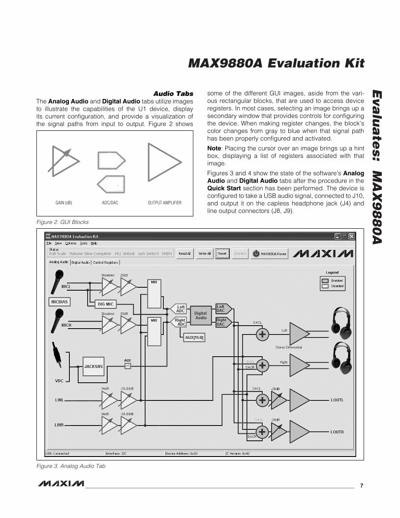
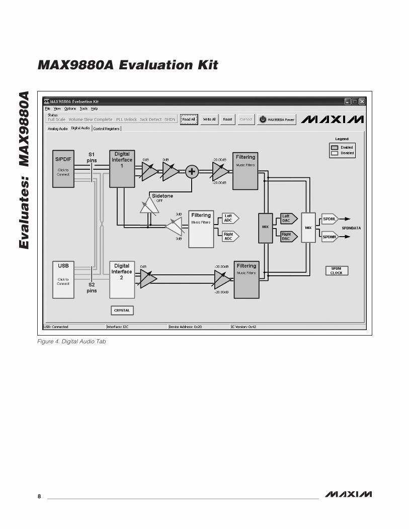
Audio TabsThe Analog Audio and Digital Audio tabs utilize images to illustrate the capabilities of the U1 device, display its current configuration, and provide a visualization of the signal paths from input to output. Figure 2 shows
some of the different GUI images, aside from the vari-ous rectangular blocks, that are used to access device registers. In most cases, selecting an image brings up a secondary window that provides controls for configuring the device. When making register changes, the block’s color changes from gray to blue when that signal path has been properly configured and activated.
Note: Placing the cursor over an image brings up a hint box, displaying a list of registers associated with that image.
Figures 3 and 4 show the state of the software’s Analog Audio and Digital Audio tabs after the procedure in the Quick Start section has been performed. The device is configured to take a USB audio signal, connected to J10, and output it on the capless headphone jack (J4) and line output connectors (J8, J9).
Figure 2. GUI Blocks
Figure 3. Analog Audio Tab
GAIN (dB) ADC/DAC OUTPUT AMPLIFIER
MAX9880A Evaluation Kit
Eva
lua
tes:
M
AX
98
80
A
8 ______________________________________________________________________________________
Figure 4. Digital Audio Tab
MAX9880A Evaluation Kit
Eva
lua
tes: M
AX
98
80
A
_______________________________________________________________________________________ 9
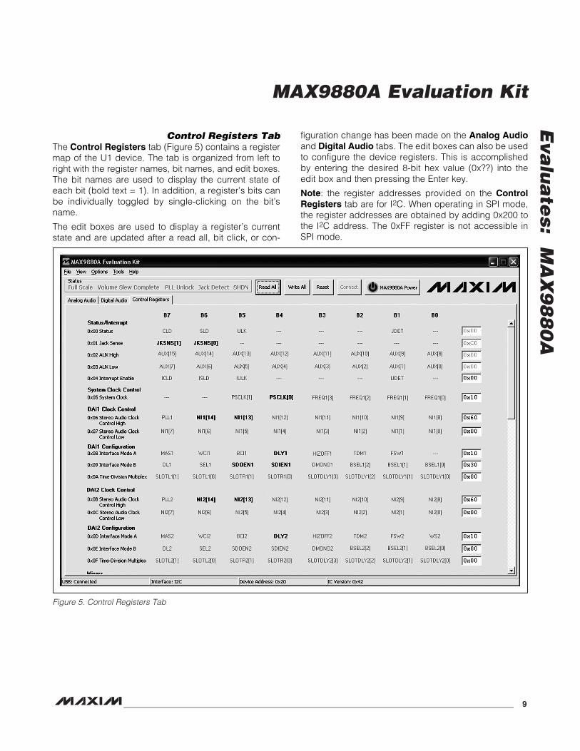
Figure 5. Control Registers Tab
Control Registers TabThe Control Registers tab (Figure 5) contains a register map of the U1 device. The tab is organized from left to right with the register names, bit names, and edit boxes. The bit names are used to display the current state of each bit (bold text = 1). In addition, a register’s bits can be individually toggled by single-clicking on the bit’s name.
The edit boxes are used to display a register’s current state and are updated after a read all, bit click, or con-
figuration change has been made on the Analog Audio and Digital Audio tabs. The edit boxes can also be used to configure the device registers. This is accomplished by entering the desired 8-bit hex value (0x??) into the edit box and then pressing the Enter key.
Note: the register addresses provided on the Control Registers tab are for I2C. When operating in SPI mode, the register addresses are obtained by adding 0x200 to the I2C address. The 0xFF register is not accessible in SPI mode.
MAX9880A Evaluation Kit
Eva
lua
tes:
M
AX
98
80
A
10 _____________________________________________________________________________________
Figure 6. S/PDIF Transceiver Window
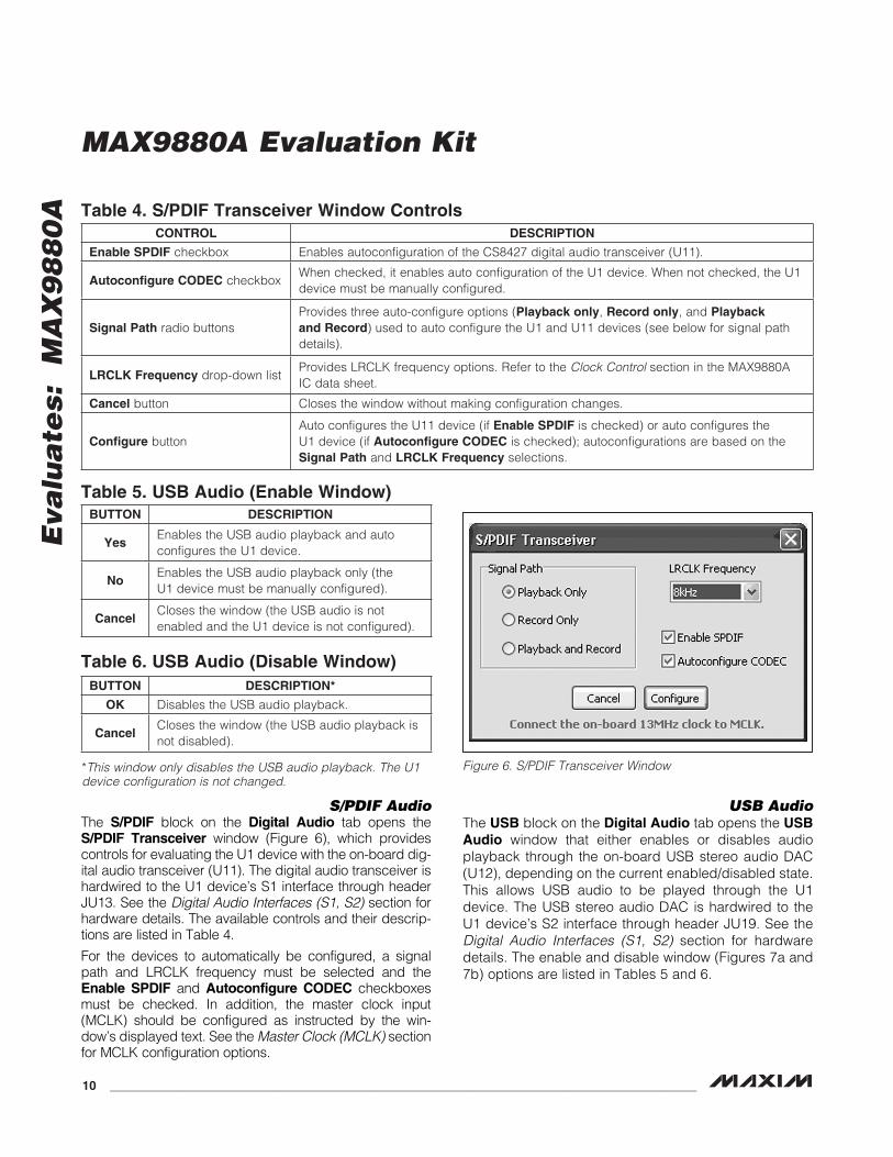
S/PDIF AudioThe S/PDIF block on the Digital Audio tab opens the S/PDIF Transceiver window (Figure 6), which provides controls for evaluating the U1 device with the on-board dig-ital audio transceiver (U11). The digital audio transceiver is hardwired to the U1 device’s S1 interface through header JU13. See the Digital Audio Interfaces (S1, S2) section for hardware details. The available controls and their descrip-tions are listed in Table 4.
For the devices to automatically be configured, a signal path and LRCLK frequency must be selected and the Enable SPDIF and Autoconfigure CODEC checkboxes must be checked. In addition, the master clock input (MCLK) should be configured as instructed by the win-dow’s displayed text. See the Master Clock (MCLK) section for MCLK configuration options.
USB AudioThe USB block on the Digital Audio tab opens the USB Audio window that either enables or disables audio playback through the on-board USB stereo audio DAC (U12), depending on the current enabled/disabled state. This allows USB audio to be played through the U1 device. The USB stereo audio DAC is hardwired to the U1 device’s S2 interface through header JU19. See the Digital Audio Interfaces (S1, S2) section for hardware details. The enable and disable window (Figures 7a and 7b) options are listed in Tables 5 and 6.
Table 4. S/PDIF Transceiver Window Controls
Table 5. USB Audio (Enable Window)
Table 6. USB Audio (Disable Window)
*This window only disables the USB audio playback. The U1 device configuration is not changed.
CONTROL DESCRIPTION
Enable SPDIF checkbox Enables autoconfiguration of the CS8427 digital audio transceiver (U11).
Autoconfigure CODEC checkboxWhen checked, it enables auto configuration of the U1 device. When not checked, the U1 device must be manually configured.
Signal Path radio buttonsProvides three auto-configure options (Playback only, Record only, and Playback and Record) used to auto configure the U1 and U11 devices (see below for signal path details).
LRCLK Frequency drop-down listProvides LRCLK frequency options. Refer to the Clock Control section in the MAX9880A IC data sheet.
Cancel button Closes the window without making configuration changes.
Configure buttonAuto configures the U11 device (if Enable SPDIF is checked) or auto configures the U1 device (if Autoconfigure CODEC is checked); autoconfigurations are based on the Signal Path and LRCLK Frequency selections.
BUTTON DESCRIPTION
YesEnables the USB audio playback and auto configures the U1 device.
NoEnables the USB audio playback only (the U1 device must be manually configured).
CancelCloses the window (the USB audio is not enabled and the U1 device is not configured).
BUTTON DESCRIPTION*
OK Disables the USB audio playback.
CancelCloses the window (the USB audio playback is not disabled).
MAX9880A Evaluation Kit
Eva
lua
tes: M
AX
98
80
A
______________________________________________________________________________________ 11
Status RegisterThe Status group box provides labels that report the state of the Status register bits (CLD, SLD, ULK, JDET) and the SHDN bit (see Table 7). The other status regis-ters (Jack Status, AUX) are reported on their individual windows. Jack Status can be monitored by selecting the JACKSNS block, and the AUX registers are report-ed on the Auxiliary Configuration window, which is accessed by selecting the AUX[15:0] block. See the Jack Detection and ADC Input Register sections.
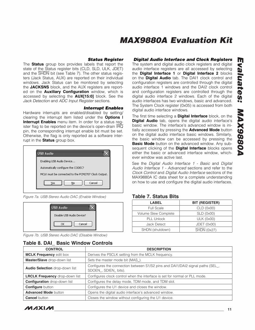
Interrupt EnablesHardware interrupts are enabled/disabled by setting/clearing the interrupt item listed under the Options | Interrupt Enables menu item. In order for a status reg-ister flag to be reported on the device’s open-drain IRQ pin, the corresponding interrupt enable bit must be set. Otherwise, the flag is only reported as a software inter-rupt in the Status group box.
Digital Audio Interface and Clock RegistersThe system and digital audio clock registers and digital audio interface registers are all accessed by selecting the Digital Interface 1 or Digital Interface 2 blocks on the Digital Audio tab. The DAI1 clock control and configuration registers are controlled through the digital audio interface 1 windows and the DAI2 clock control and configuration registers are controlled through the digital audio interface 2 windows. Each of the digital audio interfaces has two windows, basic and advanced. The System Clock register (0x05) is accessed from both digital audio interface windows.
The first time selecting a Digital Interface block, on the Digital Audio tab, opens the digital audio interface’s basic window. The interface’s advanced window is ini-tially accessed by pressing the Advanced Mode button on the digital audio interface basic windows. Similarly, the basic window can be accessed by pressing the Basic Mode button on the advanced window. Any sub-sequent clicking of the Digital Interface blocks opens either the basic or advanced interface window, which-ever window was active last.
See the Digital Audio Interface 1 - Basic and Digital Audio Interface 1 - Advanced sections and refer to the Clock Control and Digital Audio Interface sections of the MAX9880A IC data sheet for a complete understanding on how to use and configure the digital audio interfaces.
Figure 7a. USB Stereo Audio DAC (Enable Window)
Figure 7b. USB Stereo Audio DAC (Disable Window)
Table 7. Status Bits
Table 8. DAI_ Basic Window Controls
LABEL BIT (REGISTER)
Full Scale CLD (0x00)
Volume Slew Complete SLD (0x00)
PLL Unlock ULK (0x00)
Jack Detect JDET (0x00)
SHDN (shutdown) SHDN (0x27)
CONTROL DESCRIPTION
MCLK Frequency edit box Derives the PSCLK setting from the MCLK frequency.
Master/Slave drop-down list Sets the master mode bit (MAS_).
Audio Selection drop-down listConfigures the connection between S1/S2 pins and DAI1/DAI2 signal paths (SEL_, SDOEN_, SDIEN_ bits).
LRCLK Frequency drop-down list Configures clock control when the interface is set for normal or PLL mode.
Configuration drop-down list Configures the delay mode, TDM mode, and TDM slot.
Configure button Configures the U1 device and closes the window.
Advanced Mode button Opens the digital audio interface’s advanced window.
Cancel button Closes the window without configuring the U1 device.
MAX9880A Evaluation Kit
Eva
lua
tes:
M
AX
98
80
A
12 _____________________________________________________________________________________
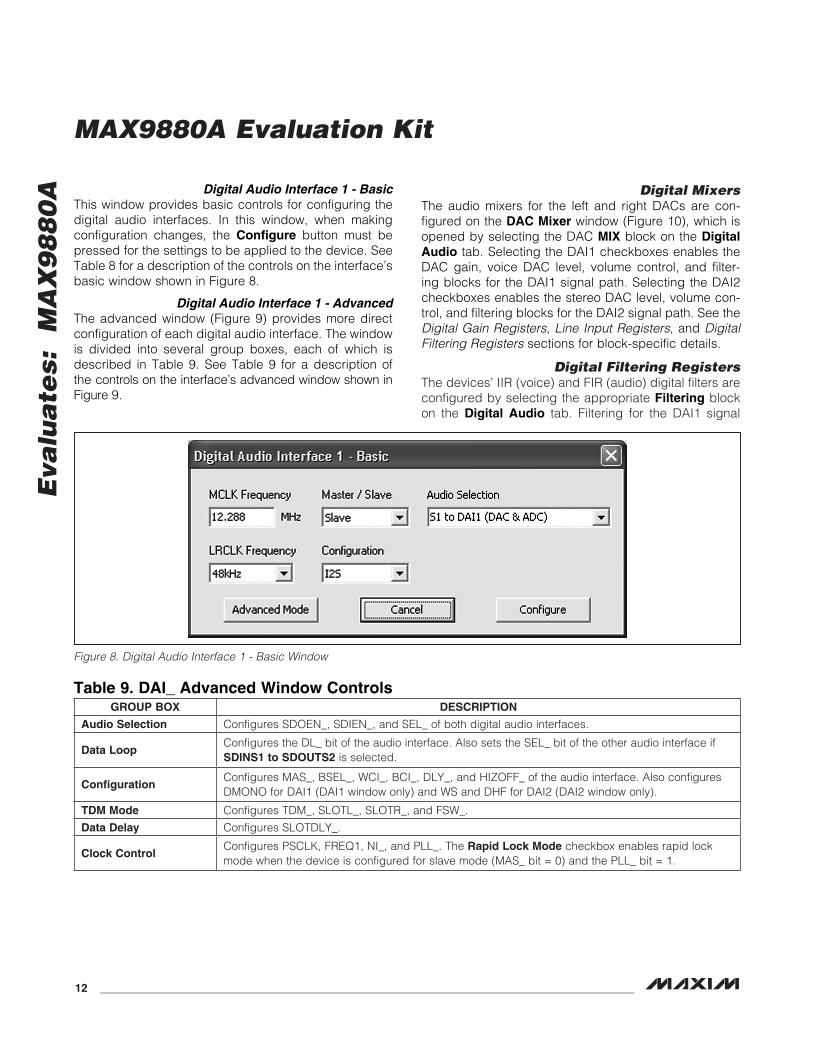
Digital Audio Interface 1 - BasicThis window provides basic controls for configuring the digital audio interfaces. In this window, when making configuration changes, the Configure button must be pressed for the settings to be applied to the device. See Table 8 for a description of the controls on the interface’s basic window shown in Figure 8.
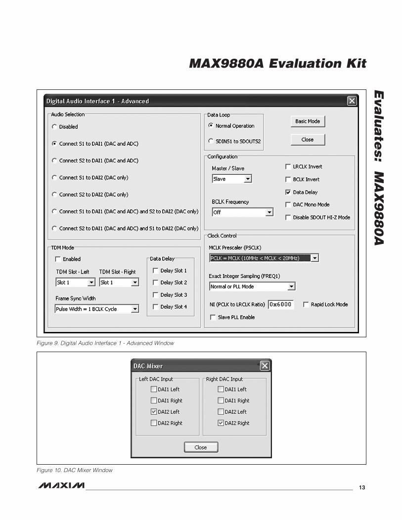
Digital Audio Interface 1 - AdvancedThe advanced window (Figure 9) provides more direct configuration of each digital audio interface. The window is divided into several group boxes, each of which is described in Table 9. See Table 9 for a description of the controls on the interface’s advanced window shown in Figure 9.
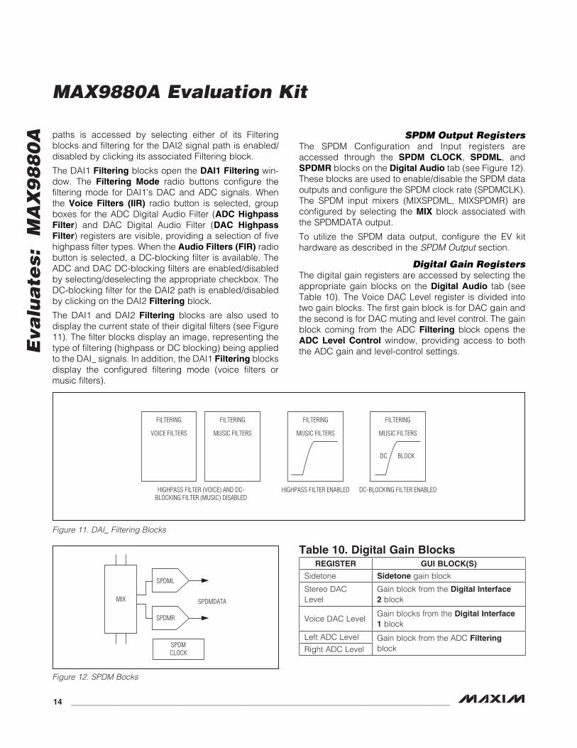
Digital MixersThe audio mixers for the left and right DACs are con-figured on the DAC Mixer window (Figure 10), which is opened by selecting the DAC MIX block on the Digital Audio tab. Selecting the DAI1 checkboxes enables the DAC gain, voice DAC level, volume control, and filter-ing blocks for the DAI1 signal path. Selecting the DAI2 checkboxes enables the stereo DAC level, volume con-trol, and filtering blocks for the DAI2 signal path. See the Digital Gain Registers, Line Input Registers, and Digital Filtering Registers sections for block-specific details.
Digital Filtering RegistersThe devices’ IIR (voice) and FIR (audio) digital filters are configured by selecting the appropriate Filtering block on the Digital Audio tab. Filtering for the DAI1 signal
Figure 8. Digital Audio Interface 1 - Basic Window
Table 9. DAI_ Advanced Window ControlsGROUP BOX DESCRIPTION
Audio Selection Configures SDOEN_, SDIEN_, and SEL_ of both digital audio interfaces.
Data LoopConfigures the DL_ bit of the audio interface. Also sets the SEL_ bit of the other audio interface if SDINS1 to SDOUTS2 is selected.
ConfigurationConfigures MAS_, BSEL_, WCI_, BCI_, DLY_, and HIZOFF_ of the audio interface. Also configures DMONO for DAI1 (DAI1 window only) and WS and DHF for DAI2 (DAI2 window only).
TDM Mode Configures TDM_, SLOTL_, SLOTR_, and FSW_.
Data Delay Configures SLOTDLY_.
Clock ControlConfigures PSCLK, FREQ1, NI_, and PLL_. The Rapid Lock Mode checkbox enables rapid lock mode when the device is configured for slave mode (MAS_ bit = 0) and the PLL_ bit = 1.
MAX9880A Evaluation Kit
Eva
lua
tes: M
AX
98
80
A
______________________________________________________________________________________ 13
Figure 9. Digital Audio Interface 1 - Advanced Window
Figure 10. DAC Mixer Window
MAX9880A Evaluation Kit
Eva
lua
tes:
M
AX
98
80
A
14 _____________________________________________________________________________________
paths is accessed by selecting either of its Filtering blocks and filtering for the DAI2 signal path is enabled/disabled by clicking its associated Filtering block.
The DAI1 Filtering blocks open the DAI1 Filtering win-dow. The Filtering Mode radio buttons configure the filtering mode for DAI1’s DAC and ADC signals. When the Voice Filters (IIR) radio button is selected, group boxes for the ADC Digital Audio Filter (ADC Highpass Filter) and DAC Digital Audio Filter (DAC Highpass Filter) registers are visible, providing a selection of five highpass filter types. When the Audio Filters (FIR) radio button is selected, a DC-blocking filter is available. The ADC and DAC DC-blocking filters are enabled/disabled by selecting/deselecting the appropriate checkbox. The DC-blocking filter for the DAI2 path is enabled/disabled by clicking on the DAI2 Filtering block.
The DAI1 and DAI2 Filtering blocks are also used to display the current state of their digital filters (see Figure 11). The filter blocks display an image, representing the type of filtering (highpass or DC blocking) being applied to the DAI_ signals. In addition, the DAI1 Filtering blocks display the configured filtering mode (voice filters or music filters).
SPDM Output RegistersThe SPDM Configuration and Input registers are accessed through the SPDM CLOCK, SPDML, and SPDMR blocks on the Digital Audio tab (see Figure 12). These blocks are used to enable/disable the SPDM data outputs and configure the SPDM clock rate (SPDMCLK). The SPDM input mixers (MIXSPDML, MIXSPDMR) are configured by selecting the MIX block associated with the SPDMDATA output.
To utilize the SPDM data output, configure the EV kit hardware as described in the SPDM Output section.
Digital Gain RegistersThe digital gain registers are accessed by selecting the appropriate gain blocks on the Digital Audio tab (see Table 10). The Voice DAC Level register is divided into two gain blocks. The first gain block is for DAC gain and the second is for DAC muting and level control. The gain block coming from the ADC Filtering block opens the ADC Level Control window, providing access to both the ADC gain and level-control settings.
Figure 11. DAI_ Filtering Blocks
Figure 12. SPDM Bocks
Table 10. Digital Gain Blocks
FILTERING
VOICE FILTERS
HIGHPASS FILTER (VOICE) AND DC-BLOCKING FILTER (MUSIC) DISABLED
HIGHPASS FILTER ENABLED DC-BLOCKING FILTER ENABLED
FILTERING
MUSIC FILTERS
FILTERING
MUSIC FILTERS
FILTERING
MUSIC FILTERS
DC BLOCK
MIX
SPDMCLOCK
SPDML
SPDMDATA
SPDMR
REGISTER GUI BLOCK(S)
Sidetone Sidetone gain block
Stereo DAC Level
Gain block from the Digital Interface 2 block
Voice DAC LevelGain blocks from the Digital Interface 1 block
Left ADC Level Gain block from the ADC Filtering blockRight ADC Level
MAX9880A Evaluation Kit
Eva
lua
tes: M
AX
98
80
A
______________________________________________________________________________________ 15
Line Input RegistersThe mute and gain settings for the line inputs (LINL and RINL) are accessed by selecting the first gain block on their respective input signal path. The gain blocks open the Left Line Input and Right Line Input windows, each of which provides controls to mute, enable, and config-ure the gain of the respective line input.
Playback Volume Registers (Line inputs, DAC inputs)
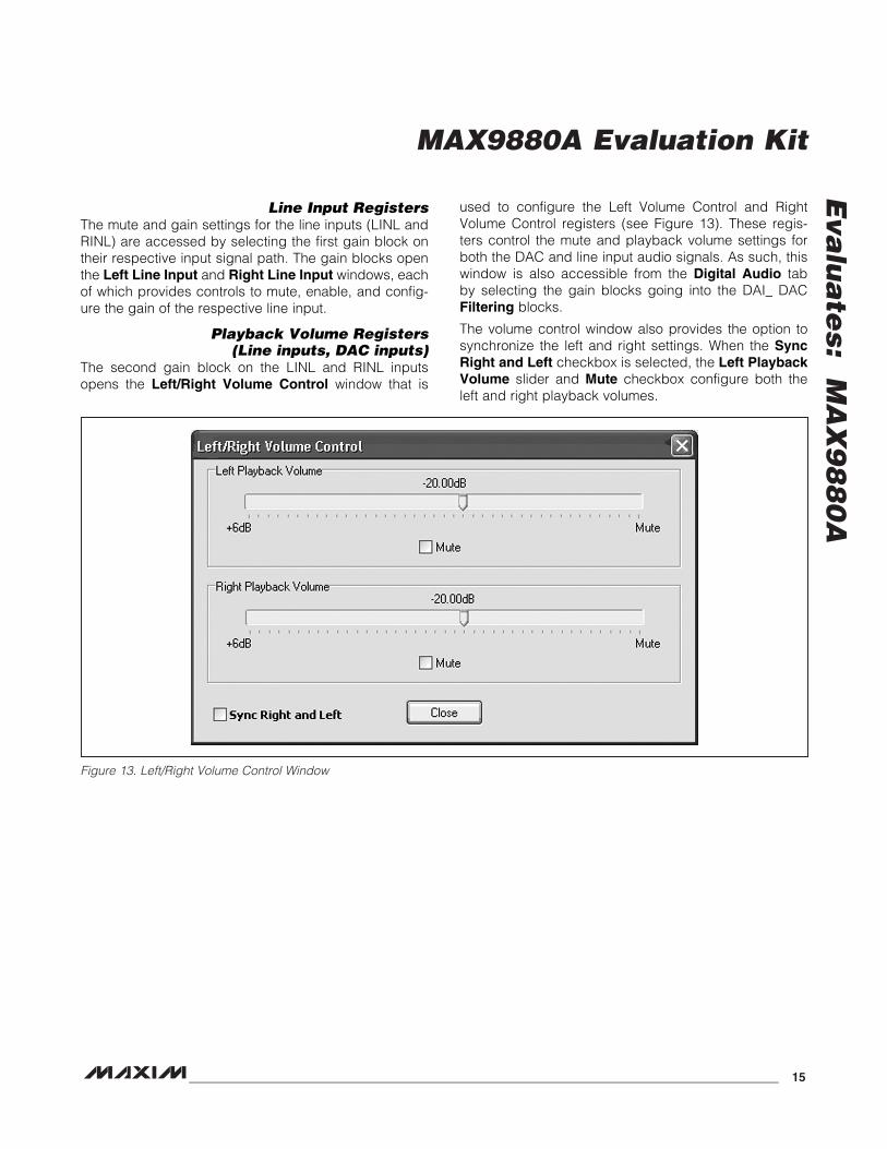
The second gain block on the LINL and RINL inputs opens the Left/Right Volume Control window that is
used to configure the Left Volume Control and Right Volume Control registers (see Figure 13). These regis-ters control the mute and playback volume settings for both the DAC and line input audio signals. As such, this window is also accessible from the Digital Audio tab by selecting the gain blocks going into the DAI_ DAC Filtering blocks.
The volume control window also provides the option to synchronize the left and right settings. When the Sync Right and Left checkbox is selected, the Left Playback Volume slider and Mute checkbox configure both the left and right playback volumes.
Figure 13. Left/Right Volume Control Window
MAX9880A Evaluation Kit
Eva
lua
tes:
M
AX
98
80
A
16 _____________________________________________________________________________________
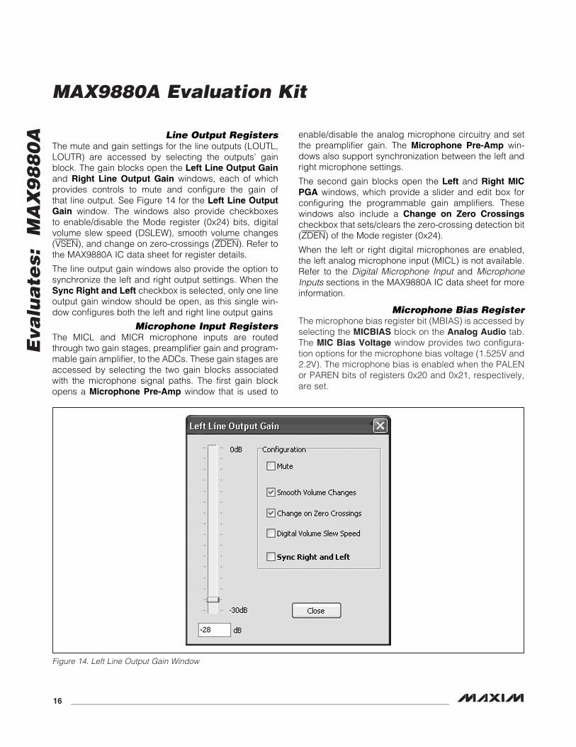
Line Output RegistersThe mute and gain settings for the line outputs (LOUTL, LOUTR) are accessed by selecting the outputs’ gain block. The gain blocks open the Left Line Output Gain and Right Line Output Gain windows, each of which provides controls to mute and configure the gain of that line output. See Figure 14 for the Left Line Output Gain window. The windows also provide checkboxes to enable/disable the Mode register (0x24) bits, digital volume slew speed (DSLEW), smooth volume changes (VSEN), and change on zero-crossings (ZDEN). Refer to the MAX9880A IC data sheet for register details.
The line output gain windows also provide the option to synchronize the left and right output settings. When the Sync Right and Left checkbox is selected, only one line output gain window should be open, as this single win-dow configures both the left and right line output gains
Microphone Input RegistersThe MICL and MICR microphone inputs are routed through two gain stages, preamplifier gain and program-mable gain amplifier, to the ADCs. These gain stages are accessed by selecting the two gain blocks associated with the microphone signal paths. The first gain block opens a Microphone Pre-Amp window that is used to
enable/disable the analog microphone circuitry and set the preamplifier gain. The Microphone Pre-Amp win-dows also support synchronization between the left and right microphone settings.
The second gain blocks open the Left and Right MIC PGA windows, which provide a slider and edit box for configuring the programmable gain amplifiers. These windows also include a Change on Zero Crossings checkbox that sets/clears the zero-crossing detection bit (ZDEN) of the Mode register (0x24).
When the left or right digital microphones are enabled, the left analog microphone input (MICL) is not available. Refer to the Digital Microphone Input and Microphone Inputs sections in the MAX9880A IC data sheet for more information.
Microphone Bias RegisterThe microphone bias register bit (MBIAS) is accessed by selecting the MICBIAS block on the Analog Audio tab. The MIC Bias Voltage window provides two configura-tion options for the microphone bias voltage (1.525V and 2.2V). The microphone bias is enabled when the PALEN or PAREN bits of registers 0x20 and 0x21, respectively, are set.
Figure 14. Left Line Output Gain Window
MAX9880A Evaluation Kit
Eva
lua
tes: M
AX
98
80
A
______________________________________________________________________________________ 17
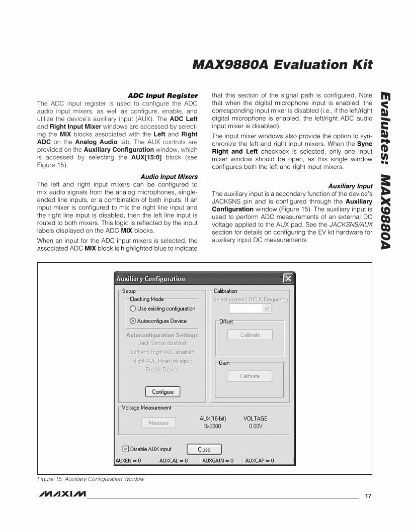
ADC Input RegisterThe ADC input register is used to configure the ADC audio input mixers, as well as configure, enable, and utilize the device’s auxiliary input (AUX). The ADC Left and Right Input Mixer windows are accessed by select-ing the MIX blocks associated with the Left and Right ADC on the Analog Audio tab. The AUX controls are provided on the Auxiliary Configuration window, which is accessed by selecting the AUX[15:0] block (see Figure 15).
Audio Input MixersThe left and right input mixers can be configured to mix audio signals from the analog microphones, single-ended line inputs, or a combination of both inputs. If an input mixer is configured to mix the right line input and the right line input is disabled, then the left line input is routed to both mixers. This logic is reflected by the input labels displayed on the ADC MIX blocks.
When an input for the ADC input mixers is selected, the associated ADC MIX block is highlighted blue to indicate
that this section of the signal path is configured. Note that when the digital microphone input is enabled, the corresponding input mixer is disabled (i.e., if the left/right digital microphone is enabled, the left/right ADC audio input mixer is disabled).
The input mixer windows also provide the option to syn-chronize the left and right input mixers. When the Sync Right and Left checkbox is selected, only one input mixer window should be open, as this single window configures both the left and right input mixers.
Auxiliary InputThe auxiliary input is a secondary function of the device’s JACKSNS pin and is configured through the Auxiliary Configuration window (Figure 15). The auxiliary input is used to perform ADC measurements of an external DC voltage applied to the AUX pad. See the JACKSNS/AUX section for details on configuring the EV kit hardware for auxiliary input DC measurements.
Figure 15. Auxiliary Configuration Window
MAX9880A Evaluation Kit
Eva
lua
tes:
M
AX
98
80
A
18 _____________________________________________________________________________________
The two top group boxes (Setup and Calibration) represent the procedures for properly configuring the ADC for performing DC voltage measurements. The first time this window is opened, the Calibration and Voltage Measurement group boxes are disabled. This is inten-tional and ensures that the ADC gets properly configured before the first DC measurement is taken. Refer to the ADC section in the MAX9880A IC data sheet for detailed steps for configuring the device.
The Setup group box contains a Clocking Mode group box that provides radio buttons to determine how the device should be set up. As there are specific device-configuration requirements, the Autoconfigure Device option is recommended, unless it is known that the cur-rent device configuration meets the setup requirements. The disabled labels are associated with the autoconfigu-ration option and display the settings that are applied once the Configure button is pressed.
Once the configuration is complete, the Offset group box is activated, enabling the second step, offset calibration. If the Use existing configuration (manual operation) is selected, the Select current LRCLK Frequency drop-down list is also activated; otherwise, it stays disabled. Pressing the offset Calibrate button executes the proce-dure listed in the Offset Calibration Procedure section of the MAX9880A IC data sheet.
Once the offset calibration sequence is complete, the Gain group box is activated, enabling the final step, gain calibration. Pressing the gain Calibrate button executes the procedure listed in the Gain Calibration Procedure section of the MAX9880A IC data sheet. The result (K) of the gain calibration is displayed below the gain Calibrate button.
After the calibration sequences are completed, the Voltage Measurement group box is activated and the device is ready to perform DC measurements. Pressing the Measure button executes the procedure listed in the DC Measurement Procedure of the MAX9880A IC data sheet. The result is displayed both as a voltage and a 16-bit hex value. Additional DC measurements are per-formed by pressing the Measure button again.
Digital Microphone Input RegisterUsing the on-board digital microphones requires both hardware and software configuration. See the Microphone Inputs section for hardware configuration options. For software configuration, select the DIG MIC block on the Analog Audio tab. The digital microphone clock is set by selecting one of the radio button options, and the left/right digital microphone inputs are enabled by checking the corresponding checkbox on the Digital Microphone Input window. When using either of the dig-ital microphone inputs, the left analog microphone input is not available. Similarly, the left/right ADC input mixers are disabled when the left/right digital microphones are enabled.
Mode RegisterThe Mode register is used to configure slew speed (DSLEW), volume-change smoothing (VSEN), line input zero-crossing detection (ZDEN), and headphone ampli-fier mode (HPMODE). The DSLEW, VSEN, and ZDEN settings are configurable through the Left Line Output Gain and Right Line Output Gain windows; addition-ally, the ZDEN setting can be configured through the Left MIC PGA and Right MIC PGA windows.
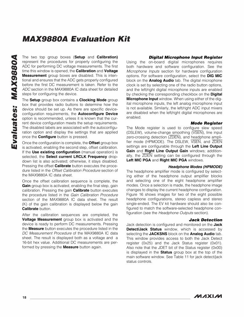
Headphone Modes (HPMODE)The headphone amplifier mode is configured by select-ing either of the headphone output amplifier blocks and selecting one of the eight headphone amplifier modes. Once a selection is made, the headphone image changes to display the current headphone configuration. Figure 16 shows images for two of the eight possible headphone configurations, stereo capless and stereo single-ended. The EV kit hardware should also be con-figured to match the software-selected headphone con-figuration (see the Headphone Outputs section).
Jack DetectionJack detection is configured and monitored on the Jack Detect/Jack Status window, which is accessed by selecting the JACKSNS block on the Analog Audio tab. This window provides access to both the Jack Detect register (0x25) and the Jack Status register (0x01). Also note that the JDET bit of the Status register (0x00) is displayed in the Status group box at the top of the main software window. See Table 11 for jack detect/jack status controls.
MAX9880A Evaluation Kit
Eva
lua
tes: M
AX
98
80
A
______________________________________________________________________________________ 19
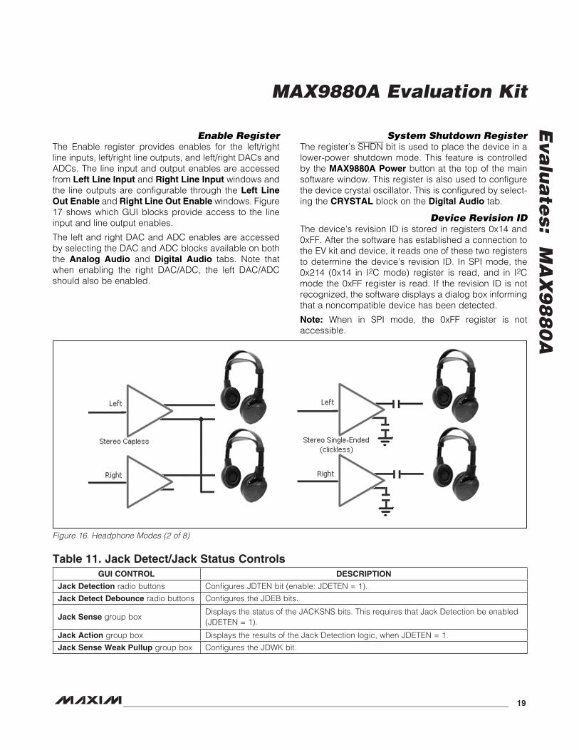
Enable RegisterThe Enable register provides enables for the left/right line inputs, left/right line outputs, and left/right DACs and ADCs. The line input and output enables are accessed from Left Line Input and Right Line Input windows and the line outputs are configurable through the Left Line Out Enable and Right Line Out Enable windows. Figure 17 shows which GUI blocks provide access to the line input and line output enables.
The left and right DAC and ADC enables are accessed by selecting the DAC and ADC blocks available on both the Analog Audio and Digital Audio tabs. Note that when enabling the right DAC/ADC, the left DAC/ADC should also be enabled.
System Shutdown RegisterThe register’s SHDN bit is used to place the device in a lower-power shutdown mode. This feature is controlled by the MAX9880A Power button at the top of the main software window. This register is also used to configure the device crystal oscillator. This is configured by select-ing the CRYSTAL block on the Digital Audio tab.
Device Revision IDThe device’s revision ID is stored in registers 0x14 and 0xFF. After the software has established a connection to the EV kit and device, it reads one of these two registers to determine the device’s revision ID. In SPI mode, the 0x214 (0x14 in I2C mode) register is read, and in I2C mode the 0xFF register is read. If the revision ID is not recognized, the software displays a dialog box informing that a noncompatible device has been detected.
Note: When in SPI mode, the 0xFF register is not accessible.
Figure 16. Headphone Modes (2 of 8)
Table 11. Jack Detect/Jack Status ControlsGUI CONTROL DESCRIPTION
Jack Detection radio buttons Configures JDTEN bit (enable: JDETEN = 1).
Jack Detect Debounce radio buttons Configures the JDEB bits.
Jack Sense group boxDisplays the status of the JACKSNS bits. This requires that Jack Detection be enabled (JDETEN = 1).
Jack Action group box Displays the results of the Jack Detection logic, when JDETEN = 1.
Jack Sense Weak Pullup group box Configures the JDWK bit.
MAX9880A Evaluation Kit
Eva
lua
tes:
M
AX
98
80
A
20 _____________________________________________________________________________________
Figure 17. Line Input and Output Enable Blocks
Save/Load SettingsRegister configurations can be saved/loaded by select-ing the Save Settings CTRL+S or Load Settings CTRL+O menu item from the File menu bar. The save operation saves the state of the U1 device registers, S/PDIF transceiver (U11) registers, and a few general-purpose input-output (GPIO) settings to a configura-tion file. The load operation configures the U1 and U11 device registers and sets/clears specific GPIO pins based on the data and settings contained in the con-figuration file.
A Configuration 1.ax27 file is included in the MAX9880A software directory and contains the data and settings that result from performing the procedure in the Quick Start section. The default and recommended file exten-sion is .ax27.
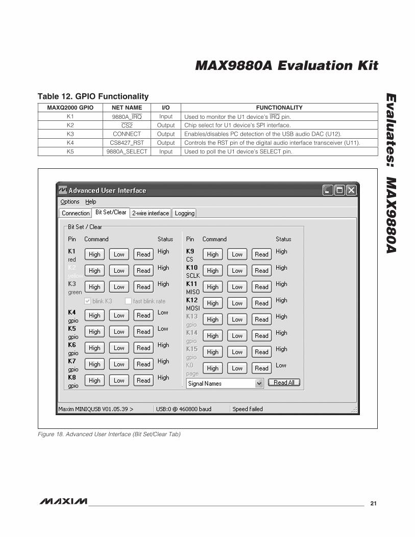
Advanced User InterfaceThe Advanced User Interface window can also be used to communicate with the U1 and U11 devices. Use the Tools | Interface (Advanced Users) F1 menu item to open the interface window, which can be used for SPI communication, I2C/SMBus™ communication, and to control the MAXQ2000 GPIOs that the EV kit utilizes. This window consists of four main tabs: Connection, Bit Set/Clear, 2-wire Interface, and 3-wire Interface (see Figure 18). The interface utility only accepts and outputs hexadecimal number format.
ConnectThe Connection tab is used to establish a connection with the MAXQ2000 interface included on the EV kit.
Bit Set/ClearThe Bit Set/Clear tab provides control of the MAXQ2000’s available GPIO pins. The only GPIO pins utilized by the EV kit are listed in Table 12, along with their functionality.
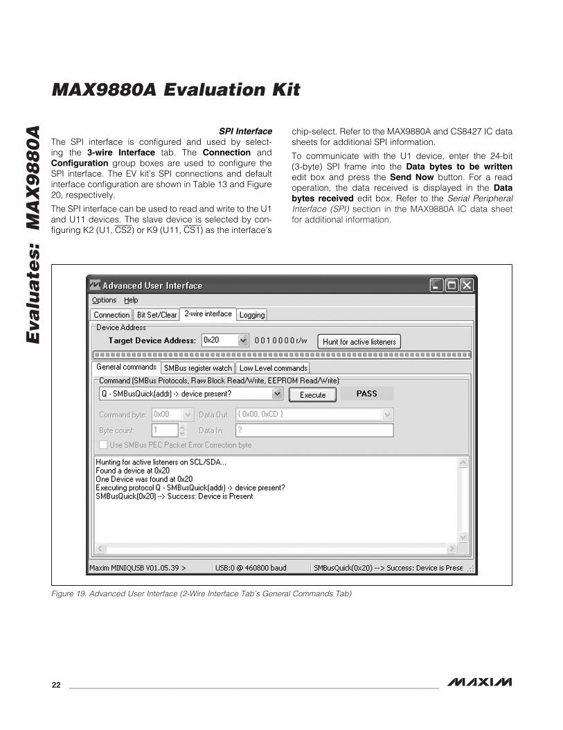
2-Wire InterfaceThe 2-wire interface tab’s General commands tab (Figure 19) allows general-purpose 2-wire commands to be sent using the Command (SMBus Protocols, Raw Block Read/Write, EEPROM Read/Write) drop-down list and the Execute button. The read/write commands to use with the U1 device are SMBusWriteByte and SMBusReadByte. The SMBusWriteByte transmits the device address, command, and 1 byte of data. The SMBusReadByte transmits the device address, a com-mand, and then retransmits the device address and reads 1 byte of data.
The device address used by the commands is the value displayed in the Target Device Address drop-down list, which is generated by pressing the Hunt for active listeners button. This button scans the entire 2-wire address space, reporting each address that is acknowledged. For both a read and write operation, the Command Byte is the register address. The data to write to the target device should be entered in the Data Out field and the data that is read is reported in the Data In field. The SCL frequency can also be configured by selecting the Low Level commands tab and using the speed buttons and/or edit fields to set the operating frequency.
SMBus is a trademark of Intel Corp.
MAX9880A Evaluation Kit
Eva
lua
tes: M
AX
98
80
A
______________________________________________________________________________________ 21
Figure 18. Advanced User Interface (Bit Set/Clear Tab)
Table 12. GPIO FunctionalityMAXQ2000 GPIO NET NAME I/O FUNCTIONALITY
K1 9880A_IRQ Input Used to monitor the U1 device’s IRQ pin.K2 CS2 Output Chip select for U1 device’s SPI interface.
K3 CONNECT Output Enables/disables PC detection of the USB audio DAC (U12).
K4 CS8427_RST Output Controls the RST pin of the digital audio interface transceiver (U11).
K5 9880A_SELECT Input Used to poll the U1 device’s SELECT pin.
MAX9880A Evaluation Kit
Eva
lua
tes:
M
AX
98
80
A
22 _____________________________________________________________________________________
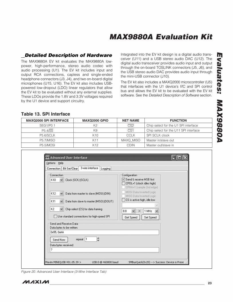
SPI InterfaceThe SPI interface is configured and used by select-ing the 3-wire Interface tab. The Connection and Configuration group boxes are used to configure the SPI interface. The EV kit’s SPI connections and default interface configuration are shown in Table 13 and Figure 20, respectively.
The SPI interface can be used to read and write to the U1 and U11 devices. The slave device is selected by con-figuring K2 (U1, CS2) or K9 (U11, CS1) as the interface’s
chip-select. Refer to the MAX9880A and CS8427 IC data sheets for additional SPI information.
To communicate with the U1 device, enter the 24-bit (3-byte) SPI frame into the Data bytes to be written edit box and press the Send Now button. For a read operation, the data received is displayed in the Data bytes received edit box. Refer to the Serial Peripheral Interface (SPI) section in the MAX9880A IC data sheet for additional information.
Figure 19. Advanced User Interface (2-Wire Interface Tab’s General Commands Tab)
MAX9880A Evaluation Kit
Eva
lua
tes: M
AX
98
80
A
______________________________________________________________________________________ 23
Detailed Description of HardwareThe MAX9880A EV kit evaluates the MAX9880A low-power, high-performance, stereo audio codec with audio processing (U1). The EV kit includes input and output RCA connections, capless and single-ended headphone connectors (J3, J4), and two on-board digital microphones (U15, U16). The EV kit also includes USB-powered low-dropout (LDO) linear regulators that allow the EV kit to be evaluated without any external supplies. These LDOs provide the 1.8V and 3.3V voltages required by the U1 device and support circuitry.
Integrated into the EV kit design is a digital audio trans-ceiver (U11) and a USB stereo audio DAC (U12). The digital audio transceiver provides audio input and output through the on-board TOSLINK connectors (J5, J6), and the USB stereo audio DAC provides audio input through the mini-USB connector (J10).
The EV kit also includes a MAXQ2000 microcontroller (U5) that interfaces with the U1 device’s I2C and SPI control bus and allows the EV kit to be evaluated with the EV kit software. See the Detailed Description of Software section.
Figure 20. Advanced User Interface (3-Wire Interface Tab)
Table 13. SPI InterfaceMAXQ2000 SPI INTERFACE MAXQ2000 GPIO NET NAME FUNCTION
SEG1/P0.1 K2 CS2 Chip select for the U1 SPI interface
P5.4/SS K9 CS1 Chip select for the U11 SPI interface
P5.6/SCLK K10 CCLK SPI SCLK clock
P5.7/MISO K11 MAXQ_MISO Master in/slave out
P5.5/MOSI K12 CDIN Master out/slave in
MAX9880A Evaluation Kit
Eva
lua
tes:
M
AX
98
80
A
24 _____________________________________________________________________________________
Master Clock (MCLK)The EV kit provides jumper JU12 to select the source of the device’s master clock input (see Table 14). The MCLK input can be connected to GND, RMCK, FUNC2, or the on-board 13MHz crystal oscillator (Y2). When connected to RMCK or FUNC2, the clock signal is provided by the digital audio transceiver or the USB stereo audio DAC, respectively.
Interface Configuration (JU21)The U1 device is configured for I2C/2-wire or SPI operation through jumper JU21 (see Table 15). Once the interface mode is configured, the shunts on headers JU20 and JU27 need to be configured, as shown in Table 16. Note that the JU20 and JU27 headers should be configured in an exclusive-or manner (i.e., only one header is shunted at a time). Once all three headers are properly configured, the PC-based EV kit software can be used to configure and control the device. See the Detailed Description of Software section.
Refer to the Serial Peripheral Interface (SPI) and I2C Serial Interface sections in the MAX9880A IC data sheet for addi-tional SPI and I2C details.
Microphone InputsThe U1 device can be evaluated with digital microphones and/or analog microphones. The EV kit provides the capa-bility to evaluate the device with only digital microphones, only analog microphones, or a combination of both types (see Table 17). The left analog microphone connects across the MICLN and MICLP pads and the right analog microphone connects across the MICRN and MICRP pads. Both single-ended and differential analog microphones can be used with the EV kit (see Table 18). Two digital microphones (U15, U16) are included on the EV kit and are connected to the device’s left microphone inputs (MICLN, MICLP) through jumpers JU8 and JU9.
Microphone Bias (JU3, JU4)The U1 device’s microphone bias (MICBIAS) output can be used to power two external analog microphones by install-ing shunts on jumpers JU3 and JU4. If digital microphones are used remove the shunt from jumper JU4.
When using the digital microphones, remove the shunts from jumpers JU5 and JU6 and leave the left microphone input pads (MICLN, MICLP) unconnected. Similarly, when using the SPDM output, remove the shunts from jumpers JU1 and JU2 and leave the right microphone input pads (MICRN, MICRP) unconnected. See the SPDM Output section.
Table 14. JU12 Function
Table 15. JU21 Function
Table 16. JU20 and JU27 Function
*Default position.
*Default position.
*Default position.
SHUNT POSITION U1 MCLK INPUT FREQUENCY
1-2 Connected to ground —
1-3 Connected to pin 10 (RMCK) of U11 MCLK = 256 x S/PDIF input sample rate
1-4* Connected to on-board crystal oscillator Y2 MCLK = 13MHz
1-5 Connected to pin 18 (FUNC2) of U12 MCLK = 256 x USB input sample rate
U1 INTERFACE
SHUNT POSITIONDESCRIPTION
JU20 JU27
I2C/2-wire*Pins 2-3 of each
row*Not installed*
The U1 device’s I2C interface is connected to the EV kit’s I2C con-trol bus.
SPI Not installedPins 2-3 of each
rowThe U1 device’s SPI interface is connected to the EV kit’s SPI con-trol bus.
SHUNT POSITION U1 SELECT PIN DESCRIPTION
Installed* Connected to ground U1 device interface = I2C/2-wire
Not installed Connected to DVDDIO through resistor R39 U1 device interface = SPI
MAX9880A Evaluation Kit
Eva
lua
tes: M
AX
98
80
A
______________________________________________________________________________________ 25
SPDM OutputThe U1 device provides an SPDM output by retask-ing the MICRN and MICRP device pins. This feature is selectable through I2C and is accessed through the SPDM blocks on the Digital Audio tab. When utilizing the SPDM output, the MICRN and MICRP pads cannot be used for microphone input and shunts should be removed from jumpers JU1 and JU2.
To access the SPDM output signals, shunts must be installed on jumpers JU18 and JU24. This configuration connects the SPDM output (SPDMDATA, SPDMCLK) to the DSD_DATA and DSD_CLK pads.
JACKSNS/AUXThe U1 device’s JACKSNS/AUX pin has dual functional-ity, allowing it to be used as an input for jack detection, or as an input for measuring DC voltages.
Jack Detection (JACKSNS)To utilize this feature, configure jumper JU7 according to Table 19, disable the AUX block on the Analog Audio tab, and refer to the Mode Configuration section in the MAX9880A IC data sheet for additional details and con-figuration options. Once the EV kit is configured for jack detection, there is one of three methods for utilizing this feature: through the JACKSNS pad, through the J3 head-phone jack, or through the MICLP pad, which requires that a shunt be installed on jumper JU29.
Table 17. Microphone Input Configuration
Table 18. Analog Microphone Configuration
*Default position.
X = Don’t care.
Table 19. JU7 Function
*Default position.
SHUNT POSITIONMICROPHONE INPUTS DESCRIPTION
JU8 JU9
Not installed Not installed Two analog microphones*Analog microphones connected across MICLN, MICLP, MICRN, and MICRP pads.
Installed installed Two digital microphonesOn-board digital microphones (U15 and U16) connected to device’s left microphone inputs.
Installed InstalledAnalog and digital micro-
phones
On-board digital microphones (U15 and U16) connected to left microphone inputs and analog microphone connected across MICRN and MICRP pads.
ANALOG MICROPHONESHUNT POSITION
JU1 JU2 JU5 JU6 JU3 JU4
Single-ended (without MICBIAS) X Installed Installed X Not installed Not installed
Single-ended (with MICBIAS) X Not installed Not installed X Installed Installed
Differential (without MICBIAS) Installed Not installed Not installed Installed Not installed Not installed
Differential (with MICBIAS) Installed Not installed Not installed Installed Installed Installed
SHUNT POSITION U1 JACKSNS/AUX PIN MODE
Installed Connected to the JACKSNS pad Jack detection
Not installed*Connected to the AUX pad through resistor-dividers R5
(10kI) and R6 (10kI)DC voltage measurements
MAX9880A Evaluation Kit
Eva
lua
tes:
M
AX
98
80
A
26 _____________________________________________________________________________________
Measuring DC Voltages (AUX)To utilize this feature, configure jumper JU7 according to Table 19, remove the shunt from jumper JU29, ensure that a headphone plug is not plugged in to jumper JU3, and enable the AUX block on the Analog Audio tab, and refer to the ADC section in the MAX9880A IC data sheet for setup and configuration details. The applied DC voltage (VAUX) is divided down before measured by the device’s ADC. The measured DC voltage (VDC) is:
DC AUXR5
V x V(R5 R6)
=+
where the default divider ratio is equal to 1/2.
Audio Inputs and OutputsThe U1 device’s audio inputs and outputs are routed to the various connectors, headers, and pads on the EV kit. Table 20 lists the audio input connections and Table 21 lists the audio output connections. Refer to the MAX9880A IC data sheet and EV kit software for audio signal routing details (i.e., which audio inputs can be routed to the available audio outputs).
Headphone OutputsThe U1 device supports three headphone output modes, single-ended, differential, and capacitorless. All three modes can be evaluated using the ROUT_ and LOUT_
pads provided on the EV kit, in conjunction with the JU10 and JU11 jumpers. Refer to the Headphone Modes sec-tion of the MAX9880A IC data sheet.
To facilitate evaluation with single-ended and capaci-torless output modes, the EV kit provides two 3.5mm headphone jacks (J3, J4). The J4 headphone jack is configured for capacitorless output mode and the J3 headphone jack is configured for single-ended output mode.
On-Board LDOsThe EV kit includes on-board LDO linear regulators (U6, U8, U9, and U10), allowing the EV kit to operate without external power supplies. These LDO regulators provide power to the U1 device’s power-supply pins: DVDD, MICVDD, PVDD, AVDD, and DVDDS1. The LDO regula-tor outputs can be isolated from the power-supply pins through jumpers JU14–JU17, and JU22, respectively.
A fifth LDO linear regulator (U7) provides power to the MAXQ2000 circuit, level translators (U4, U17), crystal oscillator (Y2), stereo digital audio transceiver (U11), USB stereo audio DAC (U12), and S/PDIF connectors (J5, J6). All the LDO linear regulators are powered by the USB bus voltage (+5V) from the J7 mini-USB connector.
Table 20. Audio Inputs Table 21. Audio Outputs
*S_ interface pins = SDOUTS_, SDINS_, BCLKS_,and LRCLKS_.
*S_ interface pins = SDOUTS_, SDINS_, BCLKS_, and LRCLKS_.
AUDIO INPUT
U1 PIN DESCRIPTION
J1 LINLSingle-ended left line input (LINEINL)
J2 LINRSingle-ended right line input (LINEINR)
J6 S1 interface* S/PDIF audio input from U11
J10 S2 interface* USB audio input from U12
MICL_ pad MICL_ Left analog microphone
MICR_ pad MICR_ Right analog microphone
U15 MICL_Left digital microphone (DIGMIC_)
U16 MICL_Right digital microphone (DIGMIC_)
AUDIO OUTPUT
U1 PIN DESCRIPTION
J3ROUTP and
LOUTPSingle-ended headphone output with jack detection
J4ROUTP, LOUTP,
and LOUTNCapless headphone output
J5 S1 interface*S/PDIF audio output on U11
J8 LOUTRSingle-ended line output (OUTR)
J9 LOUTLSingle-ended line output (OUTL)
ROUT_ pads ROUT_ Right headphone output
LOUT_ pads LOUT_ Left headphone output
MAX9880A Evaluation Kit
Eva
lua
tes: M
AX
98
80
A
______________________________________________________________________________________ 27
Digital Audio Interfaces (S1, S2)The two digital audio interfaces (S1, S2) of the U1 device are routed through headers JU13 and JU19 to the on-board digital audio transceiver (U11) and USB stereo audio DAC (U12), respectively (see Tables 24 and 25). Place shunts across all 2-3 positions to connect the U1 device’s S1 and S2 interfaces to the listed U11 and U12 interfaces.
Digital Audio Transceiver (U11)The digital audio transceiver connects to TOSLINK con-nectors J5 and J6 for audio input and output. The device is operated in software mode (HS pin tied low) and is connected to the U1 device’s S1 digital audio interface. The audio transceiver is also interfaced to the EV kit’s SPI control bus and is selected by the CS1 chip select line. See the S/PDIF Audio section.To manually configure the
device’s registers, select the Show S/PDIF Transceiver Registers item from the View drop-down menu. This enables the CS8427 tab, which functions in the same manner as the Control Registers tab. When the U11 device is enabled, the Read All button also reads all the U11 registers and updates the CS8427 tab.
USB Stereo Audio DAC (U12)The USB stereo audio DAC connects to the mini-USB connector J10 for audio input. The audio DAC uses a standard Windows class driver, and when connected to a PC it is recognized as an external sound card, allow-ing audio from a PC to be played through the EV kit. This audio path is configured and enabled by selecting the USB block on the Digital Audio tab. See the USB Audio section.
Table 23. JU14–JU17 and JU22 Functions
Table 24. S1 Interface Header (JU13) Table 25. S2 Interface Header (JU19)
*Connects to DVDDS1.**Default position.
*Signals are routed from the U4 level translator.
Table 22. JU10 and JU11 Function
*Default position.
SHUNT POSITION
HEADPHONE MODE
Installed Single-ended (clickless)
Not installed*Differential, capacitorless, or single-ended
(fast turn-on)
SHUNT POSITIONDVDD(JU14)
MICVDD(JU22)
PVDD(JU16)
AVDD(JU15)
DVDDIO*(JU17)
Installed** 1.8V 1.8V 1.8V 1.8V 3.3V
Not installed Connect an external supply across their respective pads and ground.
JU13
POSITION 1(LEFT)
POSITION 2(CENTER)
POSITION 3(RIGHT)
GND DACIN1 U11_DAC
GND ADCOUT1 U11_ADC
GND LRCLK1 U11_LRCLK
GND BCLK1 U11_BCLK
JU19
POSITION 1(LEFT)
POSITION 2(CENTER)
POSITION 3*(RIGHT)
GND DACIN2 U12_DAC
GND ADCOUT2 U12_ADC
GND LRCLK2 U12_LRCLK
GND BCLK2 U12_BCLK
MAX9880A Evaluation Kit
Eva
lua
tes:
M
AX
98
80
A
28 _____________________________________________________________________________________
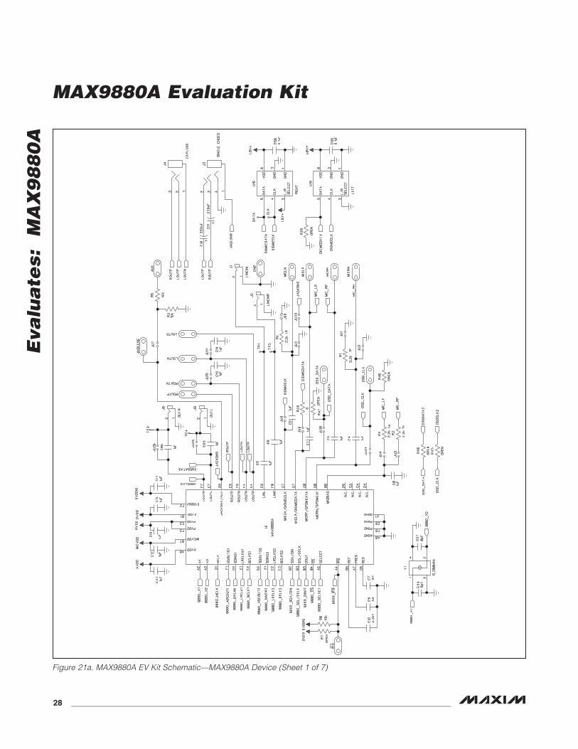
Figure 21a. MAX9880A EV Kit Schematic—MAX9880A Device (Sheet 1 of 7)
MAX9880A Evaluation Kit
Eva
lua
tes: M
AX
98
80
A
______________________________________________________________________________________ 29
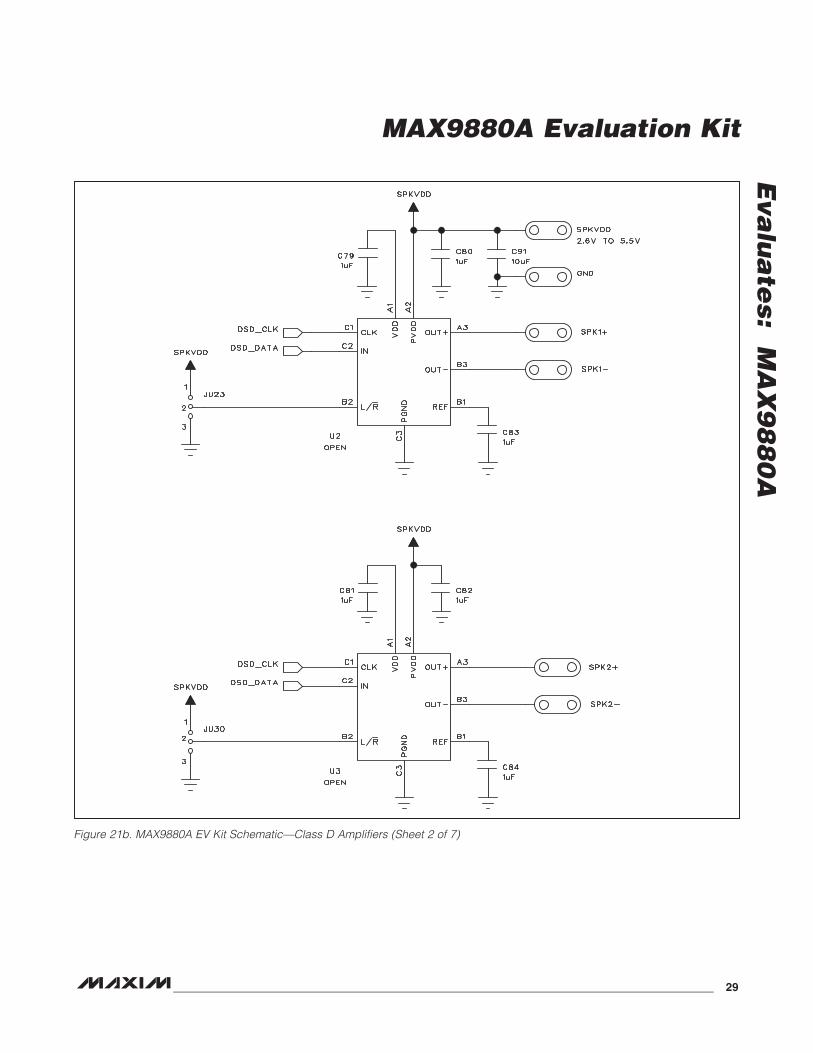
Figure 21b. MAX9880A EV Kit Schematic—Class D Amplifiers (Sheet 2 of 7)
MAX9880A Evaluation Kit
Eva
lua
tes:
M
AX
98
80
A
30 _____________________________________________________________________________________
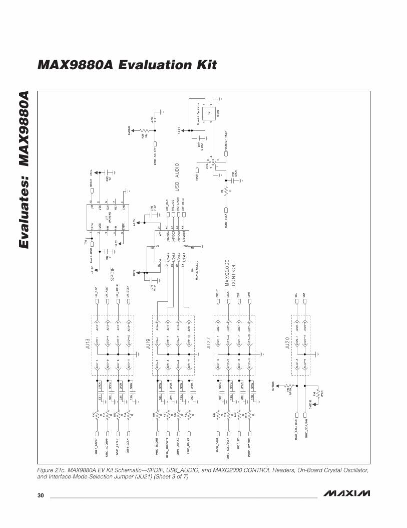
Figure 21c. MAX9880A EV Kit Schematic—SPDIF, USB_AUDIO, and MAXQ2000 CONTROL Headers, On-Board Crystal Oscillator, and Interface-Mode-Selection Jumper (JU21) (Sheet 3 of 7)
MAX9880A Evaluation Kit
Eva
lua
tes: M
AX
98
80
A
______________________________________________________________________________________ 31
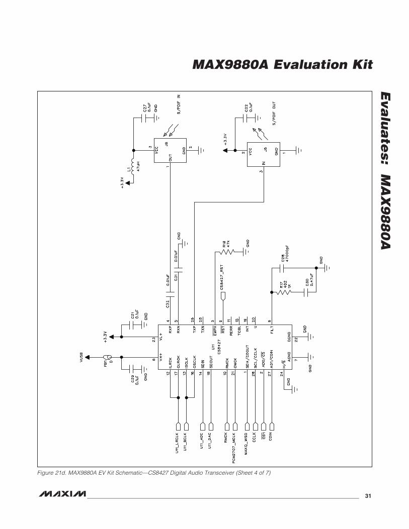
Figure 21d. MAX9880A EV Kit Schematic—CS8427 Digital Audio Transceiver (Sheet 4 of 7)
MAX9880A Evaluation Kit
Eva
lua
tes:
M
AX
98
80
A
32 _____________________________________________________________________________________
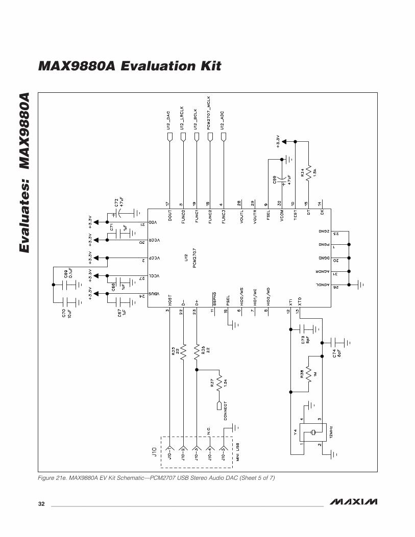
Figure 21e. MAX9880A EV Kit Schematic—PCM2707 USB Stereo Audio DAC (Sheet 5 of 7)
MAX9880A Evaluation Kit
Eva
lua
tes: M
AX
98
80
A
______________________________________________________________________________________ 33
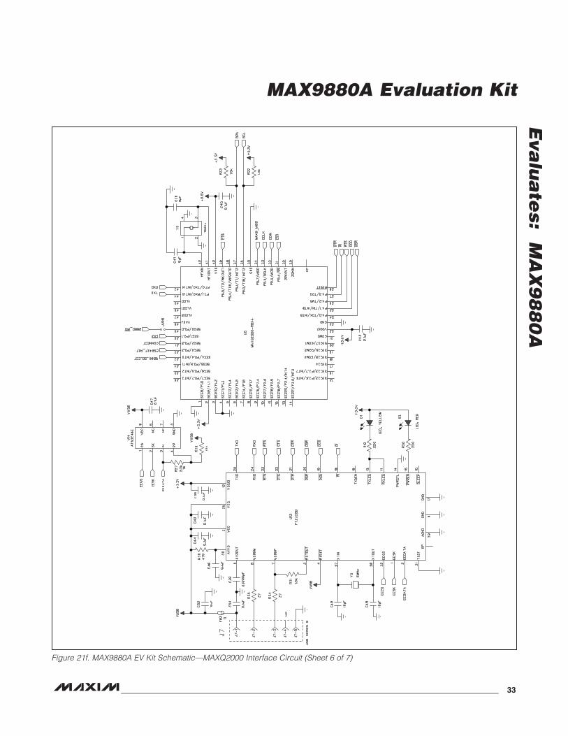
Figure 21f. MAX9880A EV Kit Schematic—MAXQ2000 Interface Circuit (Sheet 6 of 7)
MAX9880A Evaluation Kit
Eva
lua
tes:
M
AX
98
80
A
34 _____________________________________________________________________________________
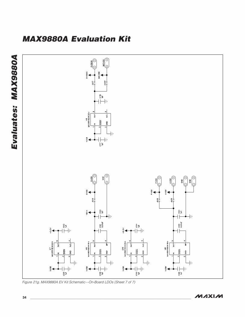
Figure 21g. MAX9880A EV Kit Schematic—On-Board LDOs (Sheet 7 of 7)
MAX9880A Evaluation Kit
Eva
lua
tes: M
AX
98
80
A
______________________________________________________________________________________ 35
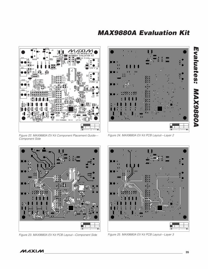
Figure 22. MAX9880A EV Kit Component Placement Guide—Component Side
Figure 23. MAX9880A EV Kit PCB Layout—Component Side
Figure 24. MAX9880A EV Kit PCB Layout—Layer 2
Figure 25. MAX9880A EV Kit PCB Layout—Layer 3
1.0” 1.0’’
1.0’’ 1.0’’
MAX9880A Evaluation Kit
Eva
lua
tes:
M
AX
98
80
A
36 _____________________________________________________________________________________
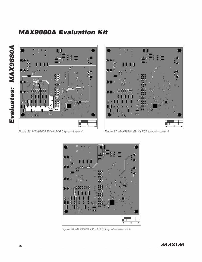
Figure 26. MAX9880A EV Kit PCB Layout—Layer 4
Figure 28. MAX9880A EV Kit PCB Layout—Solder Side
Figure 27. MAX9880A EV Kit PCB Layout—Layer 5
1.0’’1.0’’
1.0’’
Maxim cannot assume responsibility for use of any circuitry other than circuitry entirely embodied in a Maxim product. No circuit patent licenses are implied. Maxim reserves the right to change the circuitry and specifications without notice at any time.
Maxim Integrated Products, 120 San Gabriel Drive, Sunnyvale, CA 94086 408-737-7600 37
© 2011 Maxim Integrated Products Maxim is a registered trademark of Maxim Integrated Products, Inc.
MAX9880A Evaluation Kit
Eva
lua
tes: M
AX
98
80
A
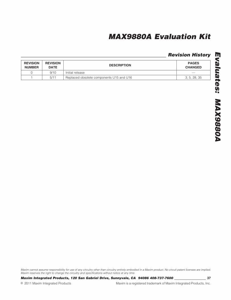
Revision History
REVISIONNUMBER
REVISION DATE
DESCRIPTIONPAGES
CHANGED
0 9/10 Initial release —
1 5/11 Replaced obsolete components U15 and U16 3, 5, 28, 35