maxrefdes73#: wearable, galvanic skin response system · construct a second-order lowpass filter...
TRANSCRIPT
MAXREFDES73#: WEARABLE, GALVANIC SKIN
RESPONSE SYSTEM
Introduction
GSR measurement detects human skin impedance under different situations. A variety of events
affect the skin impedance of a human body, such as changes with the ambient environment,
stress from a sudden event, and sweating from physical exercises. GSR devices can be used in
medical treatment, lie detection, and wellness monitoring. The MAXREFDES73# reference design
is a wrist-worn GSR measurement device that monitors both skin impedance and temperature on
a user’s wrist. With a mobile device for Android, a user can monitor his or her skin resistance and
temperature within 20m through the Bluetooth low-energy (BLE) wireless interface.
The MAX32600 microcontroller is the center of the GSR device. The MAX32600 integrates all the
analog front-end and other peripherals required for impedance measurements, including one 16-
bit ADC with input MUX and PGA, two 12-bit DACs and two 8-bit DACs, 4 operational amplifiers
(OP AMP), 4 uncommitted SPST analog switches, and internal voltage references.
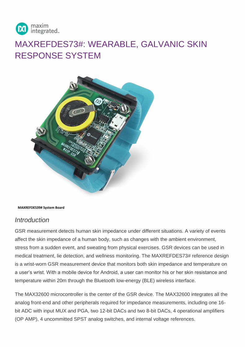
MAXREFDES39# System Board
The MAXREFDES73# reference design (Figure 1) demonstrates the typical use of a GSR device.
The developer or user can reconfigure the device through minimal firmware or hardware changes
to customize it for other specific applications. Please note, the impedance and temperature are not
calibrated. The design serves as a flexible high-performance, low-cost platform for developing
customized wearable devices.
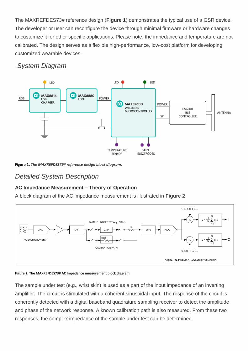
System Diagram
Figure 1, The MAXREFDES79# reference design block diagram.
Detailed System Description
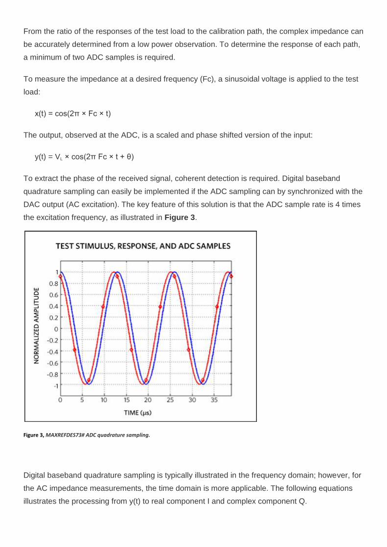
AC Impedance Measurement – Theory of Operation
A block diagram of the AC impedance measurement is illustrated in Figure 2
Figure 2, The MAXREFDES73# AC Impedance measurement block diagram
The sample under test (e.g., wrist skin) is used as a part of the input impedance of an inverting
amplifier. The circuit is stimulated with a coherent sinusoidal input. The response of the circuit is
coherently detected with a digital baseband quadrature sampling receiver to detect the amplitude
and phase of the network response. A known calibration path is also measured. From these two
responses, the complex impedance of the sample under test can be determined.
From the ratio of the responses of the test load to the calibration path, the complex impedance can
be accurately determined from a low power observation. To determine the response of each path,
a minimum of two ADC samples is required.
To measure the impedance at a desired frequency (Fc), a sinusoidal voltage is applied to the test
load:
x(t) = cos(2π × Fc × t)
The output, observed at the ADC, is a scaled and phase shifted version of the input:
y(t) = VL × cos(2π Fc × t + θ)
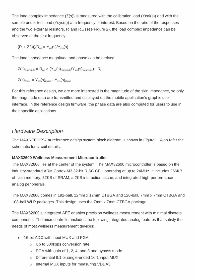
To extract the phase of the received signal, coherent detection is required. Digital baseband
quadrature sampling can easily be implemented if the ADC sampling can by synchronized with the
DAC output (AC excitation). The key feature of this solution is that the ADC sample rate is 4 times
the excitation frequency, as illustrated in Figure 3.
Figure 3, MAXREFDES73# ADC quadrature sampling.
Digital baseband quadrature sampling is typically illustrated in the frequency domain; however, for
the AC impedance measurements, the time domain is more applicable. The following equations
illustrates the processing from y(t) to real component I and complex component Q.

y(t) = VL × cos(2π Fc × t + θ)
TS = 1/(4 × Fc)
y(k) = VL × cos(π/2 × k + θ)
kΣ 0, 1, 2, ... N - 1
y(k) = VL[cosθ, cos(π/2 + θ), cos(π + θ), cos(3π/2 + θ), ...]
y(k) = VL[cosθ, - sinθ, - cosθ, sinθ, ...]
To calculate the complex impedance, we are interested in extracting the magnitude and phase
information:
VLejθ = VLcos(θ) + jVLsin(θ) = I + JQ
By observation, the first 2 ADC samples yield I and Q:
I = VLcos(θ) = y(0)
Q = VLsin(θ) = y(1)
We can split the ADC samples (even/odd) and modulate by ±1 to generate multiple observations
of the real component I and the complex component Q. Because we are processing a single
frequency, we can average these outputs to increase the SNR (signal-to-noise ratio) of the
measurements, as illustrated below:
Where N is the number of ADC samples, it is a multiple of 4.
Phase = θ = atan2(Q,I)
Magnitude = VL = √(I2 + Q2)
The load complex impedance (Z(s)) is measured with the calibration load (Ycal(s)) and with the
sample under test load (Ysys(s)) at a frequency of interest. Based on the ratio of the responses
and the two external resistors, Ri and Rcal (see Figure 2), the load complex impedance can be
observed at the test frequency:
(Ri + Z(s))/Rcal = Ycal(s)/Ysys(s)
The load impedance magnitude and phase can be derived:
Z(s)magnitude = Rcal × (Ycal(s)magnitude/Ysys(s)magnitude) - Ri
Z(s)phase = Ycal(s)phase - Ysys(s)phase
For this reference design, we are more interested in the magnitude of the skin impedance, so only
the magnitude data are transmitted and displayed on the mobile application’s graphic user
interface. In the reference design firmware, the phase data are also computed for users to use in
their specific applications.
Hardware Description
The MAXREFDES73# reference design system block diagram is shown in Figure 1. Also refer the
schematic for circuit details.
MAX32600 Wellness Measurement Microcontroller
The MAX32600 lies at the center of the system. The MAX32600 microcontroller is based on the
industry-standard ARM Cortex-M3 32-bit RISC CPU operating at up to 24MHz. It includes 256KB
of flash memory, 32KB of SRAM, a 2KB instruction cache, and integrated high-performance
analog peripherals.
The MAX32600 comes in 192-ball, 12mm x 12mm CTBGA and 120-ball, 7mm x 7mm CTBGA and
108-ball WLP packages. This design uses the 7mm x 7mm CTBGA package.
The MAX32600’s integrated AFE enables precision wellness measurement with minimal discrete
components. The microcontroller includes the following integrated analog features that satisfy the
needs of most wellness measurement devices:
16-bit ADC with input MUX and PGA
o Up to 500ksps conversion rate
o PGA with gain of 1, 2, 4, and 8 and bypass mode
o Differential 8:1 or single-ended 16:1 input MUX
o Internal MUX inputs for measuring VDDA3
Internal or external voltage reference
o Programmable buffers for ADC and DACs
Two 12-bit DACs and two 8-bit DACs
Four operational amplifiers
Four low-power comparators
Four uncommitted SPST analog switches
Four ground switches
Up to eight 100mA LED driver pairs (sink)
Internal temperature sensor
In this GSR unit design, only several ceramic capacitors and resistors are required, making the
design compact and cost effective.
Power Supply and the MAX8814 Linear Li+ Battery Charger
The MAXREFDES73# is powered by a lithium-ion rechargeable battery, the LIR2032. The battery
has a nominal voltage of 3.6V and maximum capacity of 45mAH. The battery is regulated by the
MAX8880 ultra-low IQ, low-dropout linear regulator.
The battery can be conveniently charged by a USB connection to a PC. The charging controller
MAX8814 is an intelligent, stand-alone constant-current, constant-voltage (CCCV), thermally
regulated linear charger. It is designed for charging a single-cell lithium-ion (Li+) battery. The
MAX8814 integrates the current-sense circuit, MOSFET pass element, thermal-regulation circuitry,
and eliminates the reverse-blocking Schottky diode to create the simplest and smallest charging
solution for handheld equipment.
The MAX8814 controls the charging sequence from the prequalification state through constant-
current fast-charge and the final constant-voltage charge. Proprietary thermal-regulation circuitry
limits the die temperature during fast-charging or when the IC is exposed to high ambient
temperatures, allowing maximum charging current without damaging the IC.
The MAX8814 achieves high flexibility by providing an adjustable fast-charge current through an
external resistor. The fast-charge current is set to 32mA. For a fully discharged battery, the GSR
device can be fully charged in less than two hours.
A fully charged battery can last about 15 hours with the default firmware settings. In the default
settings, the device measures the skin impedance and temperature every 1s, and transmits the
data to a mobile device through BLE wireless interface.
When the device is being charged, the yellow LED D3 turns on and the charging indication icon on
the mobile app is also turned on.
AC Impedance Measurement Circuit and Settings
The AC impedance measurement block diagram is shown in Figure 2.
Referring to the schematic, the 12-bit DAC0 generates the excitation sinusoidal signal with a 1V
peak-to-peak magnitude. The microcontroller DMA engine makes the direct digital synthesis
possible. The DAC0 output signal is buffered by OP AMP D. R17, R18, C25, C26, and OP AMP A
construct a second-order lowpass filter (LPF). C27 blocks the DC component of the excitation
signal. Four internal SPST switches dynamically reconfigure the load to either the calibration path
or human skin load. The 8-bit DAC2 generates the common-mode bias before ADC input. C29
and R25 construct a first-order LPF and gain control. Finally, R41, R42, and C47 work as a LPF
before ADC input.
The MAXREFDES73# sets the default excitation frequency at 7.8125kHz. The hardware settings
for this single fixed-frequency measurement are as follows:
Both ADC and DAC voltage references = 2.048V
DAC0 power level = 2, sine wave output frequency = 7.8125kHz, voltage = 1V peak-to-peak
DAC2 DC output voltage = 1.12V
ADC sample rate = 31.25kHz, decimation = 4, PGA gain = 2
Clock source: 24MHz internal relaxation oscillator
The MAXREFDES73# also provides a frequency sweeping function for users’ reference. The
device measures the skin impedances using excitation frequencies from 100Hz up to 15.625kHz.
After the measurement is done, the device transmits the data to the mobile device in a batch.
The hardware settings for frequency sweeping are the same as above settings except that the
following DAC0 sine wave output frequency and ADC sample rate pairs are different:
When DAC0 output frequency = 100Hz, ADC sample rate = 400Hz
When DAC0 output frequency = 200Hz, ADC sample rate = 800Hz
When DAC0 output frequency = 500Hz, ADC sample rate = 2000Hz
When DAC0 output frequency = 1kHz, ADC sample rate = 4kHz
When DAC0 output frequency = 1.953125kHz, ADC sample rate = 7.8125kHz
When DAC0 output frequency = 5kHz, ADC sample rate = 20kHz
When DAC0 output frequency = 7.8125kHz, ADC sample rate = 31.25kHz
When DAC0 output frequency = 12.5kHz, ADC sample rate = 50kHz
When DAC0 output frequency = 15.625kHz, ADC sample rate = 62.5kHz
For each measurement: 184 ADC samples are collected (46 sine wave cycles), 160 samples are
used in averaging (40 sine wave cycles), the first 6 cycles are discarded.
Temperature Measurement
The MAX32600 microcontroller includes an internal temperature sensor that can be read using the
ADC, and additionally supports a mode for an external temperature sensor, which is connected to
the same ADC input pair. Because the GSR device needs a temperature sensor that can directly
touch the user’s skin, an external negative temperature coefficient (NTC) sensor is used.
The MAXREFDES73# connects the NTC temperature sensor to MAX32600 AN1+ pin. The current
sourced onto MAX32600 AN1+ pin is programmable at 4µA, 60µA, 64µA, and 120µA respectively.
The GSR device uses an NTC temperature sensor with nominal resistance of 30.15kΩ at 37°C.
The sensor’s Steinhart–Hart parameters are:
a = 824.970719, b = 222.454876, c = 0.095600.
So, the current sourced onto AN1+ is set to 4µA (AinCurrentSel = 00).
With the ADC PGA set to 2, if the ADC code is CODE, the voltage drop on the sensor is given by
VNTC = CODE × 2.048/(65535 × 2)(V)
The resistance of the NTC sensor is given by
RNTC = VNTC/I = CODE × 2.048/(65535 × 2 × 0.000004)(Ω)
Based on third-order approximation of Steinhart–Hart equation, the temperature is given by
T = 1/(a + b × ln(RNTC) + c × (ln(RNTC))3 (Kelvin)
Bluetooth Low-Energy Controller
The MAXREFDES73# reference design provides a free companion mobile app that runs on a
mobile device for Android. The GSR device communicates with the device for Android through
BLE wireless connection. The BLE controller is EM9301 from EM Microelectronic. The MAX32600
microcontroller controls the BLE chip through an SPI interface. The MAX32600 internal LDO
output VDDIO provides power for the BLE chip. Refer the EM9301 datasheet for details.
Firmware Description
The MAXREFDES73# firmware is based on an interrupt-driven design model. After power-up, the
microcontroller configures the power domains, clock domains, DAC settings, ADC settings, other
analog peripherals, GPIO pins, SPI controller, and BLE controller hardware and software stack.
Then the device keeps sending BLE advertisement packets before a connection is set up. If a BLE
connection cannot be established within 30s, the device switches to a sleep mode until the reset
button is pressed. The green LED D2 indicates the advertisement is happening.
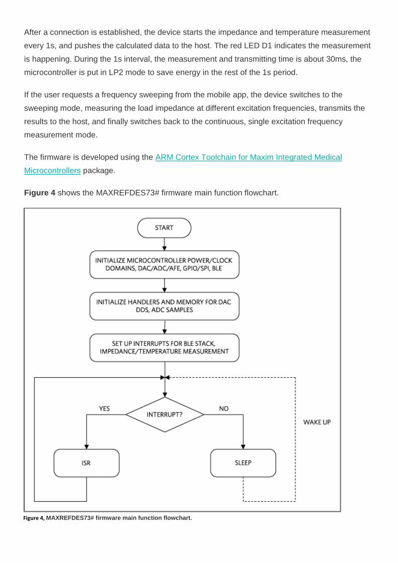
After a connection is established, the device starts the impedance and temperature measurement
every 1s, and pushes the calculated data to the host. The red LED D1 indicates the measurement
is happening. During the 1s interval, the measurement and transmitting time is about 30ms, the
microcontroller is put in LP2 mode to save energy in the rest of the 1s period.
If the user requests a frequency sweeping from the mobile app, the device switches to the
sweeping mode, measuring the load impedance at different excitation frequencies, transmits the
results to the host, and finally switches back to the continuous, single excitation frequency
measurement mode.
The firmware is developed using the ARM Cortex Toolchain for Maxim Integrated Medical
Microcontrollers package.
Figure 4 shows the MAXREFDES73# firmware main function flowchart.
Figure 4, MAXREFDES73# firmware main function flowchart.
Quick Start
Required Equipment:
Purchased from Maxim:
MAXREFDES73# reference design (GSR wrist-worn device)
User supplied:
A tablet or smart phone device for Android
Follow the ensuing procedure to verify the correct functioning of the MAXREFDES73#.
Procedure
1. Go to the Google Play store to download the latest version of the MAXREFDES73# mobile
app. In the Google Play search box, type MAXREFDES73. The app requires Android 4.3
or later.
2. Start the MAXREFDES73# mobile app.
3. Wear the MAXREFDES73# device on a wrist. Make sure the electrodes firmly touch the
wrist skin. Alternatively, use a 10kΩ resistor to connect the electrodes.
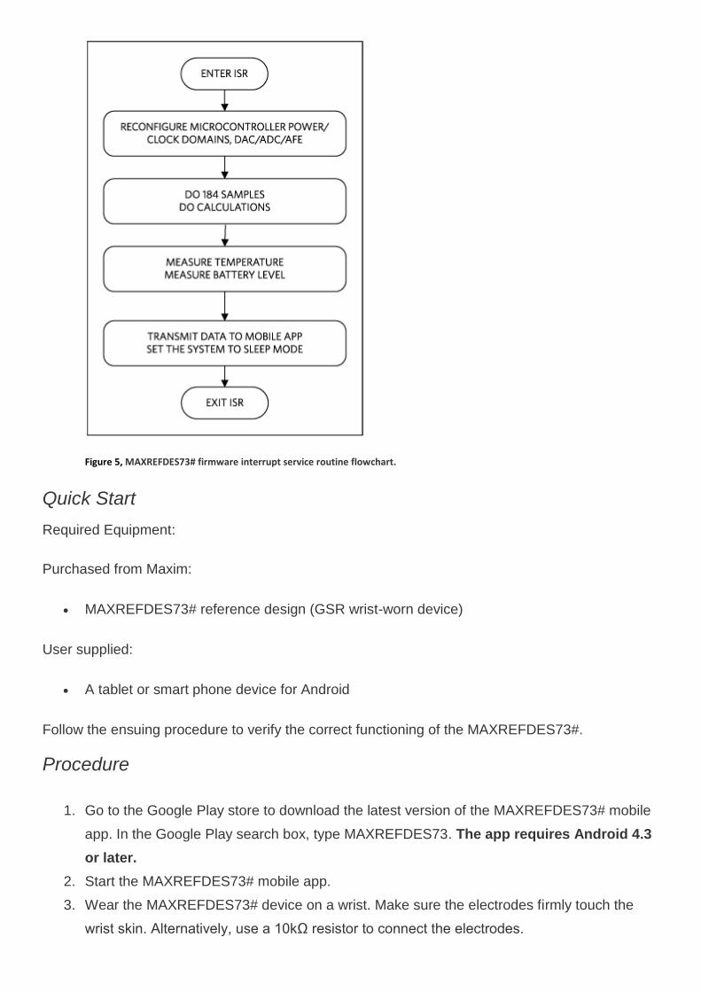
Figure 5, MAXREFDES73# firmware interrupt service routine flowchart.
4. On the device, press the pushbutton, the green LED turns on.
5. On the mobile app, when the BLE advertisement is detected, tap the device found.
6. The mobile app displays the temperature and impedance magnitude. Refreshing every 1s.
7. Verify that the red LED on the device flashes shortly every 1s.
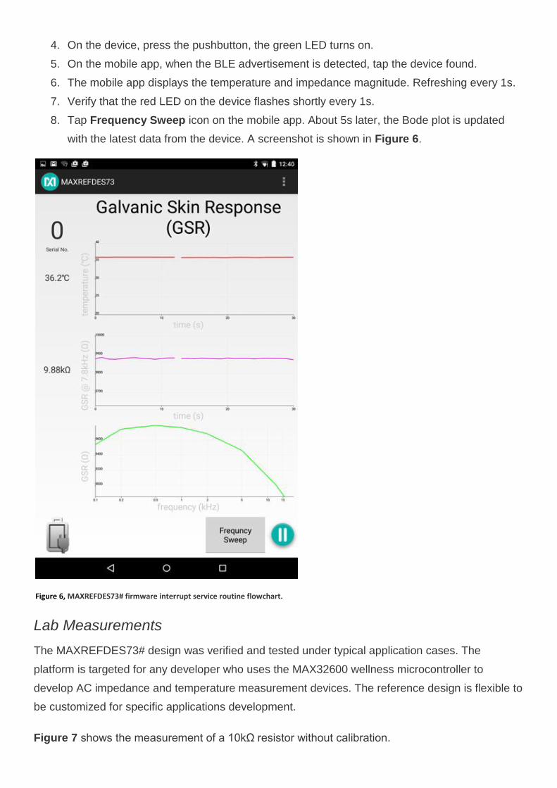
8. Tap Frequency Sweep icon on the mobile app. About 5s later, the Bode plot is updated
with the latest data from the device. A screenshot is shown in Figure 6.
Lab Measurements
The MAXREFDES73# design was verified and tested under typical application cases. The
platform is targeted for any developer who uses the MAX32600 wellness microcontroller to
develop AC impedance and temperature measurement devices. The reference design is flexible to
be customized for specific applications development.
Figure 7 shows the measurement of a 10kΩ resistor without calibration.
Figure 6, MAXREFDES73# firmware interrupt service routine flowchart.
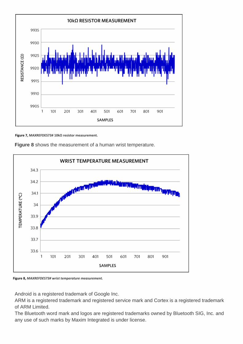
Figure 8 shows the measurement of a human wrist temperature.
Android is a registered trademark of Google Inc.
ARM is a registered trademark and registered service mark and Cortex is a registered trademark
of ARM Limited.
The Bluetooth word mark and logos are registered trademarks owned by Bluetooth SIG, Inc. and
any use of such marks by Maxim Integrated is under license.
Figure 7, MAXREFDES73# 10kΩ resistor measurement.
Figure 8, MAXREFDES73# wrist temperature measurement.

Maxim Integrated Products, Inc
All the above information was collected and can be found from
[https://www.maximintegrated.com/en/design/reference-design-center/system-board/6147.html/tb_tab1]