mc1458, mc1558 dual general-purpose operational amplifiers · mc1458, mc1558 dual general-purpose...
TRANSCRIPT

MC1458, MC1558DUAL GENERAL-PURPOSE OPERATIONAL AMPLIFIERS
SLOS069C − FEBRUARY 1971 − REVISED AUGUST 2010
1POST OFFICE BOX 655303 • DALLAS, TEXAS 75265POST OFFICE BOX 1443 • HOUSTON, TEXAS 77251−1443
� Short-Circuit Protection
� Wide Common-Mode and DifferentialVoltage Ranges
� No Frequency Compensation Required
� Low Power Consumption
� No Latch-Up
� Designed to Be Interchangeable With Motorola MC1558/MC1458 and Signetics S5558/N5558
description/ordering information
The MC1458 and MC1558 are dualgeneral-purpose operational amplifiers, with eachhalf electrically similar to the μA741, except thatoffset null capability is not provided.
The high-common-mode input voltage range andthe absence of latch-up make these amplifiersideal for voltage-follower applications. Thedevices are short-circuit protected and theinternal frequency compensation ensures stabilitywithout external components.
ORDERING INFORMATION
TAVIOmaxAT 25°C PACKAGE† ORDERABLE
PART NUMBERTOP-SIDEMARKING
PDIP (P) Tube MC1458P MC1458P
0°C to 70°C 6 mV SOIC (D)Tube MC1458D
MC14580°C to 70°C 6 mV SOIC (D)Tape and reel MC1458DR
MC1458
SOP (PS) Tape and reel MC1458PSR M1458
CDIP (JG) Tube MC1558JG MC1558JG
−55°C to 125°C 5 mV CDIP (JGB) Tube MC1558JGB MC1558JGB55 C to 125 C 5 mV
LCCC (FK) Tube MC1558FK MC1558FK† Package drawings, standard packing quantities, thermal data, symbolization, and PCB design guidelines are available at
www.ti.com/sc/package.
Copyright © 2002, Texas Instruments IncorporatedPRODUCTION DATA information is current as of publication date.Products conform to specifications per the terms of Texas Instrumentsstandard warranty. Production processing does not necessarily includetesting of all parameters.
On products compliant to MIL-PRF-38535, all parameters are testedunless otherwise noted. On all other products, productionprocessing does not necessarily include testing of all parameters.
1
2
3
4
8
7
6
5
1OUT1IN−1IN+VCC−
VCC+2OUT2IN−2IN+
(TOP VIEW)
MC1458 . . . D, P, OR PS PACKAGEMC1558 . . . JG PACKAGE
3 2 1 20 19
9 10 11 12 13
4
5
6
7
8
18
17
16
15
14
NC2OUTNC2IN−NC
NC1IN−
NC1IN+
NC
MC1558 . . . FK PACKAGE
NC
1OU
TN
C
NC
NC
NC
VN
C
NC − No internal connection
CC
+V
2IN
+
CC−
(TOP VIEW)

MC1458, MC1558DUAL GENERAL-PURPOSE OPERATIONAL AMPLIFIERS
SLOS069C − FEBRUARY 1971 − REVISED AUGUST 2010
2 POST OFFICE BOX 655303 • DALLAS, TEXAS 75265POST OFFICE BOX 1443 • HOUSTON, TEXAS 77251−1443
symbol (each amplifier)
−
+
IN+OUT
IN−
schematic (each amplifier)
IN −
IN + OUT
VCC +
VCC −

MC1458, MC1558DUAL GENERAL-PURPOSE OPERATIONAL AMPLIFIERS
SLOS069C − FEBRUARY 1971 − REVISED AUGUST 2010
3POST OFFICE BOX 655303 • DALLAS, TEXAS 75265POST OFFICE BOX 1443 • HOUSTON, TEXAS 77251−1443
absolute maximum ratings over operating free-air temperature range (unless otherwise noted)†
Supply voltage, VCC+ (see Note 1): MC1458 18 V. . . . . . . . . . . . . . . . . . . . . . . . . . . . . . . . . . . . . . . . . . . . . . . . . MC1558 22 V. . . . . . . . . . . . . . . . . . . . . . . . . . . . . . . . . . . . . . . . . . . . . . . . .
Supply voltage, VCC− (see Note 1): MC1458 −18 V. . . . . . . . . . . . . . . . . . . . . . . . . . . . . . . . . . . . . . . . . . . . . . . . MC1558 −22 V. . . . . . . . . . . . . . . . . . . . . . . . . . . . . . . . . . . . . . . . . . . . . . . .
Differential input voltage, VID (see Note 2) ±30 V. . . . . . . . . . . . . . . . . . . . . . . . . . . . . . . . . . . . . . . . . . . . . . . . . . . Input voltage, VI (either input, see Notes 1 and 3) ±15 V. . . . . . . . . . . . . . . . . . . . . . . . . . . . . . . . . . . . . . . . . . . . . Duration of output short circuit (see Note 4) Unlimited. . . . . . . . . . . . . . . . . . . . . . . . . . . . . . . . . . . . . . . . . . . . . . . Operating virtual junction temperature, TJ 150°C. . . . . . . . . . . . . . . . . . . . . . . . . . . . . . . . . . . . . . . . . . . . . . . . . . . Package thermal impedance, θJA (see Notes 5 and 6): D package 97°C/W. . . . . . . . . . . . . . . . . . . . . . . . . . . .
P package 85°C/W. . . . . . . . . . . . . . . . . . . . . . . . . . . . PS package 95°C/W. . . . . . . . . . . . . . . . . . . . . . . . . .
Package thermal impedance, θJC (see Notes 7 and 8): FK package 5.61°C/W. . . . . . . . . . . . . . . . . . . . . . . . . JG package 14.5°C/W. . . . . . . . . . . . . . . . . . . . . . . . .
Case temperature for 60 seconds: FK package 260°C. . . . . . . . . . . . . . . . . . . . . . . . . . . . . . . . . . . . . . . . . . . . . . Lead temperature 1,6 mm (1/16 inch) from case for 10 seconds: JG package 300°C. . . . . . . . . . . . . . . . . . . . Lead temperature 1,6 mm (1/16 inch) from case for 60 seconds: D, P, or PS package 260°C. . . . . . . . . . . . . Storage temperature range, Tstg −65°C to 150°C. . . . . . . . . . . . . . . . . . . . . . . . . . . . . . . . . . . . . . . . . . . . . . . . . . .
† Stresses beyond those listed under “absolute maximum ratings” may cause permanent damage to the device. These are stress ratings only, andfunctional operation of the device at these or any other conditions beyond those indicated under “recommended operating conditions” is notimplied. Exposure to absolute-maximum-rated conditions for extended periods may affect device reliability.
NOTES: 1. All voltage values, unless otherwise noted, are with respect to the midpoint between VCC+ and VCC− .2. Differential voltages are at IN+ with respect to IN−.3. The magnitude of the input voltage must never exceed the magnitude of the supply voltage or 15 V, whichever is less.4. The output can be shorted to ground or either power supply. For the MC1558 only, the unlimited duration of the short circuit applies
at (or below) 125°C case temperature or 70°C free-air temperature.5. Maximum power dissipation is a function of TJ(max), θJA, and TA. The maximum allowable power dissipation at any allowable
ambient temperature is PD = (TJ(max) − TA)/θJA. Operating at the absolute maximum TJ of 150°C can affect reliability.6. The package thermal impedance is calculated in accordance with JESD 51-7.7. Maximum power dissipation is a function of TJ(max), θJC, and TC. The maximum allowable power dissipation at any allowable case
temperature is PD = (TJ(max) − TC)/θJC. Operating at the absolute maximum TJ of 150°C can affect reliability.8. The package thermal impedance is calculated in accordance with MIL-STD-883.
recommended operating conditionsMIN MAX UNIT
VCC± Supply voltage ±5 ±15 V
T Operating free air temperature rangeMC1458 0 70
°CTA Operating free-air temperature rangeMC1558 −55 125
°C

MC1458, MC1558DUAL GENERAL-PURPOSE OPERATIONAL AMPLIFIERS
SLOS069C − FEBRUARY 1971 − REVISED AUGUST 2010
4 POST OFFICE BOX 655303 • DALLAS, TEXAS 75265POST OFFICE BOX 1443 • HOUSTON, TEXAS 77251−1443
electrical characteristics at specified free-air temperature, VCC± = ±15 V
PARAMETER TEST CONDITIONS†MC1458 MC1558
UNITPARAMETER TEST CONDITIONS†MIN TYP MAX MIN TYP MAX
UNIT
V Input offset voltage V 025°C 1 6 1 5
mVVIO Input offset voltage VO = 0Full range 7.5 6
mV
I Input offset current V 025°C 20 200 20 200
nAIIO Input offset current VO = 0Full range 300 500
nA
I Input bias current V 025°C 80 500 80 500
nAIIB Input bias current VO = 0Full range 800 1500
nA
VCommon-mode input 25°C ±12 ±13 ±12 ±13
VVICRCommon mode inputvoltage range Full range ±12 ±12
V
RL = 10 kΩ 25°C ±12 ±14 ±12 ±14
VMaximum peak output RL ≥ 10 kΩ Full range ±12 ±11
VVOMMaximum peak outputvoltage swing RL = 2 kΩ 25°C ±10 ±13 ±10 ±13
V
RL ≥ 2 kΩ Full range ±10 ±10
ALarge-signal differential
R ≥ 2 kΩ V ±10 V25°C 20 200 50 200
V/mVAVDLarge signal differentialvoltage amplification RL ≥ 2 kΩ, VO = ±10 V
Full range 15 25V/mV
BOM
Maximum-output-swingbandwidth(closed loop)
RL = 2 kΩ, VO ≥ ±10 V,AVD = 1, THD ≥ 5%
25°C 14 14 kHz
B1 Unity-gain bandwidth 25°C 1 1 MHz
φm Phase margin AVD = 1 25°C 65 65 deg
Gain margin 25°C 11 11 dB
ri Input resistance 25°C 0.3 2 0.3* 2 MΩ
ro Output resistance VO = 0, See Note 9 25°C 75 75 Ω
Ci Input capacitance 25°C 1.4 1.4 pF
zicCommon-mode inputimpedance
f = 20 Hz 25°C 200 200 MΩ
CMRRCommon-mode VIC = VICR min, 25°C 70 90 70 90
dBCMRRCommon moderejection ratio
VIC = VICR min, VO = 0 Full range 70 70
dB
kSupply-voltagesensitivity
VCC = ±9 V to ±15 V, 25°C 30 150 30 150V/VkSVS sensitivity
(ΔVIO/ΔVCC)
VCC = ±9 V to ±15 V,VO = 0 Full range 150 150
μV/V
VnEquivalent input noisevoltage (closed loop)
AVD = 100, RS = 0,f = 1 kHz, BW = 1 Hz
25°C 45 45 nV/√Hz
IOSShort-circuit outputcurrent
25°C ±25 ±40 ±25 ±40 mA
ISupply current
V 0 No load25°C 3.4 5.6 3.4 5
mAICCSupply current(both amplifiers) VO = 0, No load
Full range 6.6 6.6mA
PTotal power dissipation
V 0 No load25°C 100 170 100 150
mWPDTotal power dissipation (both amplifiers) VO = 0, No load
Full range 200 200mW
VO1/VO2 Crosstalk attenuation 25°C 120 120 dB
*On products compliant to MIL-PRF-38535, this parameter is not production tested.† All characteristics are specified under open-loop operating conditions with zero common-mode input voltage, unless otherwise specified. Full
range for MC1458 is 0°C to 70°C and for MC1558 is −55°C to 125°C.NOTE 9: This typical value applies only at frequencies above a few hundred hertz because of the effect of drift and thermal feedback.

MC1458, MC1558DUAL GENERAL-PURPOSE OPERATIONAL AMPLIFIERS
SLOS069C − FEBRUARY 1971 − REVISED AUGUST 2010
5POST OFFICE BOX 655303 • DALLAS, TEXAS 75265POST OFFICE BOX 1443 • HOUSTON, TEXAS 77251−1443
operating characteristics, VCC± = ±15 V, CL = 100 pF, TA = 25°C (see Figure 1)
PARAMETER TEST CONDITIONSMC1458 MC1558
UNITPARAMETER TEST CONDITIONSMIN TYP MAX MIN TYP MAX
UNIT
tRise time VI = 20 mV, RL = 2 kΩ, 0.3 0.3 μs
tr Overshoot factor VI = 20 mV, RL = 2 kΩ 5 5 %
SR Slew rate at unity gain VI = 10 V, RL = 2 kΩ 0.5 0.5 V/μs
PARAMETER MEASUREMENT INFORMATION
+
−
VI
0 V
Input
Output
RL = 2 kΩCL = 100 pF
Test Circuit
Input VoltageWaveform
Figure 1. Rise-Time, Overshoot, and Slew-Rate Waveform and Test Circuit

PACKAGE OPTION ADDENDUM
www.ti.com 17-Mar-2017
Addendum-Page 1
PACKAGING INFORMATION
Orderable Device Status(1)
Package Type PackageDrawing
Pins PackageQty
Eco Plan(2)
Lead/Ball Finish(6)
MSL Peak Temp(3)
Op Temp (°C) Device Marking(4/5)
Samples
5962-9760301Q2A ACTIVE LCCC FK 20 1 TBD POST-PLATE N / A for Pkg Type -55 to 125 5962-9760301Q2AMC1558FKB
5962-9760301QPA ACTIVE CDIP JG 8 1 TBD A42 N / A for Pkg Type -55 to 125 9760301QPAMC1558
MC1458D ACTIVE SOIC D 8 75 Green (RoHS& no Sb/Br)
CU NIPDAU Level-1-260C-UNLIM 0 to 70 MC1458
MC1458DE4 ACTIVE SOIC D 8 75 Green (RoHS& no Sb/Br)
CU NIPDAU Level-1-260C-UNLIM 0 to 70 MC1458
MC1458DR ACTIVE SOIC D 8 2500 Green (RoHS& no Sb/Br)
CU NIPDAU Level-1-260C-UNLIM 0 to 70 MC1458
MC1458DRE4 ACTIVE SOIC D 8 2500 Green (RoHS& no Sb/Br)
CU NIPDAU Level-1-260C-UNLIM 0 to 70 MC1458
MC1458DRG4 ACTIVE SOIC D 8 2500 Green (RoHS& no Sb/Br)
CU NIPDAU Level-1-260C-UNLIM 0 to 70 MC1458
MC1458P ACTIVE PDIP P 8 50 Pb-Free(RoHS)
CU NIPDAU N / A for Pkg Type 0 to 70 MC1458P
MC1458PE4 ACTIVE PDIP P 8 50 Pb-Free(RoHS)
CU NIPDAU N / A for Pkg Type 0 to 70 MC1458P
MC1458PSR ACTIVE SO PS 8 2000 Green (RoHS& no Sb/Br)
CU NIPDAU Level-1-260C-UNLIM 0 to 70 M1458
MC1558FKB ACTIVE LCCC FK 20 1 TBD POST-PLATE N / A for Pkg Type -55 to 125 5962-9760301Q2AMC1558FKB
MC1558JG ACTIVE CDIP JG 8 1 TBD A42 N / A for Pkg Type -55 to 125 MC1558JG
MC1558JGB ACTIVE CDIP JG 8 1 TBD A42 N / A for Pkg Type -55 to 125 9760301QPAMC1558
(1) The marketing status values are defined as follows:ACTIVE: Product device recommended for new designs.LIFEBUY: TI has announced that the device will be discontinued, and a lifetime-buy period is in effect.NRND: Not recommended for new designs. Device is in production to support existing customers, but TI does not recommend using this part in a new design.PREVIEW: Device has been announced but is not in production. Samples may or may not be available.OBSOLETE: TI has discontinued the production of the device.

PACKAGE OPTION ADDENDUM
www.ti.com 17-Mar-2017
Addendum-Page 2
(2) Eco Plan - The planned eco-friendly classification: Pb-Free (RoHS), Pb-Free (RoHS Exempt), or Green (RoHS & no Sb/Br) - please check http://www.ti.com/productcontent for the latest availabilityinformation and additional product content details.TBD: The Pb-Free/Green conversion plan has not been defined.Pb-Free (RoHS): TI's terms "Lead-Free" or "Pb-Free" mean semiconductor products that are compatible with the current RoHS requirements for all 6 substances, including the requirement thatlead not exceed 0.1% by weight in homogeneous materials. Where designed to be soldered at high temperatures, TI Pb-Free products are suitable for use in specified lead-free processes.Pb-Free (RoHS Exempt): This component has a RoHS exemption for either 1) lead-based flip-chip solder bumps used between the die and package, or 2) lead-based die adhesive used betweenthe die and leadframe. The component is otherwise considered Pb-Free (RoHS compatible) as defined above.Green (RoHS & no Sb/Br): TI defines "Green" to mean Pb-Free (RoHS compatible), and free of Bromine (Br) and Antimony (Sb) based flame retardants (Br or Sb do not exceed 0.1% by weightin homogeneous material)
(3) MSL, Peak Temp. - The Moisture Sensitivity Level rating according to the JEDEC industry standard classifications, and peak solder temperature.
(4) There may be additional marking, which relates to the logo, the lot trace code information, or the environmental category on the device.
(5) Multiple Device Markings will be inside parentheses. Only one Device Marking contained in parentheses and separated by a "~" will appear on a device. If a line is indented then it is a continuationof the previous line and the two combined represent the entire Device Marking for that device.
(6) Lead/Ball Finish - Orderable Devices may have multiple material finish options. Finish options are separated by a vertical ruled line. Lead/Ball Finish values may wrap to two lines if the finishvalue exceeds the maximum column width.
Important Information and Disclaimer:The information provided on this page represents TI's knowledge and belief as of the date that it is provided. TI bases its knowledge and belief on informationprovided by third parties, and makes no representation or warranty as to the accuracy of such information. Efforts are underway to better integrate information from third parties. TI has taken andcontinues to take reasonable steps to provide representative and accurate information but may not have conducted destructive testing or chemical analysis on incoming materials and chemicals.TI and TI suppliers consider certain information to be proprietary, and thus CAS numbers and other limited information may not be available for release.
In no event shall TI's liability arising out of such information exceed the total purchase price of the TI part(s) at issue in this document sold by TI to Customer on an annual basis.

TAPE AND REEL INFORMATION
*All dimensions are nominal
Device PackageType
PackageDrawing
Pins SPQ ReelDiameter
(mm)
ReelWidth
W1 (mm)
A0(mm)
B0(mm)
K0(mm)
P1(mm)
W(mm)
Pin1Quadrant
MC1458DR SOIC D 8 2500 330.0 12.4 6.4 5.2 2.1 8.0 12.0 Q1
MC1458DR SOIC D 8 2500 330.0 12.4 6.4 5.2 2.1 8.0 12.0 Q1
MC1458PSR SO PS 8 2000 330.0 16.4 8.2 6.6 2.5 12.0 16.0 Q1
PACKAGE MATERIALS INFORMATION
www.ti.com 14-Jul-2012
Pack Materials-Page 1

*All dimensions are nominal
Device Package Type Package Drawing Pins SPQ Length (mm) Width (mm) Height (mm)
MC1458DR SOIC D 8 2500 367.0 367.0 35.0
MC1458DR SOIC D 8 2500 340.5 338.1 20.6
MC1458PSR SO PS 8 2000 367.0 367.0 38.0
PACKAGE MATERIALS INFORMATION
www.ti.com 14-Jul-2012
Pack Materials-Page 2

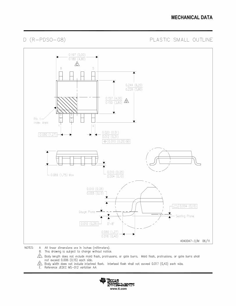


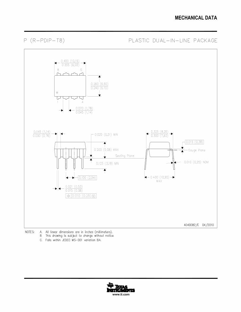
MECHANICAL DATA
MCER001A – JANUARY 1995 – REVISED JANUARY 1997
POST OFFICE BOX 655303 • DALLAS, TEXAS 75265
JG (R-GDIP-T8) CERAMIC DUAL-IN-LINE
0.310 (7,87)0.290 (7,37)
0.014 (0,36)0.008 (0,20)
Seating Plane
4040107/C 08/96
5
40.065 (1,65)0.045 (1,14)
8
1
0.020 (0,51) MIN
0.400 (10,16)0.355 (9,00)
0.015 (0,38)0.023 (0,58)
0.063 (1,60)0.015 (0,38)
0.200 (5,08) MAX
0.130 (3,30) MIN
0.245 (6,22)0.280 (7,11)
0.100 (2,54)
0°–15°
NOTES: A. All linear dimensions are in inches (millimeters).B. This drawing is subject to change without notice.C. This package can be hermetically sealed with a ceramic lid using glass frit.D. Index point is provided on cap for terminal identification.E. Falls within MIL STD 1835 GDIP1-T8

IMPORTANT NOTICE
Texas Instruments Incorporated (TI) reserves the right to make corrections, enhancements, improvements and other changes to itssemiconductor products and services per JESD46, latest issue, and to discontinue any product or service per JESD48, latest issue. Buyersshould obtain the latest relevant information before placing orders and should verify that such information is current and complete.TI’s published terms of sale for semiconductor products (http://www.ti.com/sc/docs/stdterms.htm) apply to the sale of packaged integratedcircuit products that TI has qualified and released to market. Additional terms may apply to the use or sale of other types of TI products andservices.Reproduction of significant portions of TI information in TI data sheets is permissible only if reproduction is without alteration and isaccompanied by all associated warranties, conditions, limitations, and notices. TI is not responsible or liable for such reproduceddocumentation. Information of third parties may be subject to additional restrictions. Resale of TI products or services with statementsdifferent from or beyond the parameters stated by TI for that product or service voids all express and any implied warranties for theassociated TI product or service and is an unfair and deceptive business practice. TI is not responsible or liable for any such statements.Buyers and others who are developing systems that incorporate TI products (collectively, “Designers”) understand and agree that Designersremain responsible for using their independent analysis, evaluation and judgment in designing their applications and that Designers havefull and exclusive responsibility to assure the safety of Designers' applications and compliance of their applications (and of all TI productsused in or for Designers’ applications) with all applicable regulations, laws and other applicable requirements. Designer represents that, withrespect to their applications, Designer has all the necessary expertise to create and implement safeguards that (1) anticipate dangerousconsequences of failures, (2) monitor failures and their consequences, and (3) lessen the likelihood of failures that might cause harm andtake appropriate actions. Designer agrees that prior to using or distributing any applications that include TI products, Designer willthoroughly test such applications and the functionality of such TI products as used in such applications.TI’s provision of technical, application or other design advice, quality characterization, reliability data or other services or information,including, but not limited to, reference designs and materials relating to evaluation modules, (collectively, “TI Resources”) are intended toassist designers who are developing applications that incorporate TI products; by downloading, accessing or using TI Resources in anyway, Designer (individually or, if Designer is acting on behalf of a company, Designer’s company) agrees to use any particular TI Resourcesolely for this purpose and subject to the terms of this Notice.TI’s provision of TI Resources does not expand or otherwise alter TI’s applicable published warranties or warranty disclaimers for TIproducts, and no additional obligations or liabilities arise from TI providing such TI Resources. TI reserves the right to make corrections,enhancements, improvements and other changes to its TI Resources. TI has not conducted any testing other than that specificallydescribed in the published documentation for a particular TI Resource.Designer is authorized to use, copy and modify any individual TI Resource only in connection with the development of applications thatinclude the TI product(s) identified in such TI Resource. NO OTHER LICENSE, EXPRESS OR IMPLIED, BY ESTOPPEL OR OTHERWISETO ANY OTHER TI INTELLECTUAL PROPERTY RIGHT, AND NO LICENSE TO ANY TECHNOLOGY OR INTELLECTUAL PROPERTYRIGHT OF TI OR ANY THIRD PARTY IS GRANTED HEREIN, including but not limited to any patent right, copyright, mask work right, orother intellectual property right relating to any combination, machine, or process in which TI products or services are used. Informationregarding or referencing third-party products or services does not constitute a license to use such products or services, or a warranty orendorsement thereof. Use of TI Resources may require a license from a third party under the patents or other intellectual property of thethird party, or a license from TI under the patents or other intellectual property of TI.TI RESOURCES ARE PROVIDED “AS IS” AND WITH ALL FAULTS. TI DISCLAIMS ALL OTHER WARRANTIES ORREPRESENTATIONS, EXPRESS OR IMPLIED, REGARDING RESOURCES OR USE THEREOF, INCLUDING BUT NOT LIMITED TOACCURACY OR COMPLETENESS, TITLE, ANY EPIDEMIC FAILURE WARRANTY AND ANY IMPLIED WARRANTIES OFMERCHANTABILITY, FITNESS FOR A PARTICULAR PURPOSE, AND NON-INFRINGEMENT OF ANY THIRD PARTY INTELLECTUALPROPERTY RIGHTS. TI SHALL NOT BE LIABLE FOR AND SHALL NOT DEFEND OR INDEMNIFY DESIGNER AGAINST ANY CLAIM,INCLUDING BUT NOT LIMITED TO ANY INFRINGEMENT CLAIM THAT RELATES TO OR IS BASED ON ANY COMBINATION OFPRODUCTS EVEN IF DESCRIBED IN TI RESOURCES OR OTHERWISE. IN NO EVENT SHALL TI BE LIABLE FOR ANY ACTUAL,DIRECT, SPECIAL, COLLATERAL, INDIRECT, PUNITIVE, INCIDENTAL, CONSEQUENTIAL OR EXEMPLARY DAMAGES INCONNECTION WITH OR ARISING OUT OF TI RESOURCES OR USE THEREOF, AND REGARDLESS OF WHETHER TI HAS BEENADVISED OF THE POSSIBILITY OF SUCH DAMAGES.Unless TI has explicitly designated an individual product as meeting the requirements of a particular industry standard (e.g., ISO/TS 16949and ISO 26262), TI is not responsible for any failure to meet such industry standard requirements.Where TI specifically promotes products as facilitating functional safety or as compliant with industry functional safety standards, suchproducts are intended to help enable customers to design and create their own applications that meet applicable functional safety standardsand requirements. Using products in an application does not by itself establish any safety features in the application. Designers mustensure compliance with safety-related requirements and standards applicable to their applications. Designer may not use any TI products inlife-critical medical equipment unless authorized officers of the parties have executed a special contract specifically governing such use.Life-critical medical equipment is medical equipment where failure of such equipment would cause serious bodily injury or death (e.g., lifesupport, pacemakers, defibrillators, heart pumps, neurostimulators, and implantables). Such equipment includes, without limitation, allmedical devices identified by the U.S. Food and Drug Administration as Class III devices and equivalent classifications outside the U.S.TI may expressly designate certain products as completing a particular qualification (e.g., Q100, Military Grade, or Enhanced Product).Designers agree that it has the necessary expertise to select the product with the appropriate qualification designation for their applicationsand that proper product selection is at Designers’ own risk. Designers are solely responsible for compliance with all legal and regulatoryrequirements in connection with such selection.Designer will fully indemnify TI and its representatives against any damages, costs, losses, and/or liabilities arising out of Designer’s non-compliance with the terms and provisions of this Notice.
Mailing Address: Texas Instruments, Post Office Box 655303, Dallas, Texas 75265Copyright © 2017, Texas Instruments Incorporated