mcdp2900 displayport1.4 to hdmi2.0a protocol … sheets/megachips pdfs/mcdp2900...megachips’...
TRANSCRIPT

MegaChips’ Proprietary Information – Strictly Confidential
Page 1 of 48
MCDP2900
DisplayPort1.4 to HDMI2.0a protocol converter with HDCP2.2 repeater
Datasheet
Rev. D
MegaChips’ Proprietary and Confidential
This information shall not be shared or distributed outside the company and will be exchanged based on the
signed proprietary information exchange agreement. MegaChips reserves the right to make any change
herein at any time without prior notice. MegaChips does not assume any responsibility or liability arising out
of application or use of any product or service described herein except as explicitly agreed upon.

MCDP2900
MegaChips’ Proprietary Information – Strictly Confidential
Page 2 of 48
Contents
1. Description.................................................................................................................................................. 9
2. Application overview ................................................................................................................................. 10
2.1. Adaptor application ........................................................................................................................... 10
2.2. Docking station application ............................................................................................................... 10
2.3. TV Application ................................................................................................................................... 11
3. System block diagram .............................................................................................................................. 11
4. Interface description ................................................................................................................................. 12
4.1. Input interface ................................................................................................................................... 12
4.1.1. Video stream regeneration ........................................................................................................ 12
4.1.2. Horizontal blanking expansion ................................................................................................... 13
4.1.3. On-chip video pattern generation .............................................................................................. 13
4.1.4. Audio stream regeneration ........................................................................................................ 13
4.1.5. HDCP RX ................................................................................................................................... 13
4.2. Output interface ................................................................................................................................. 13
4.2.1. HDMI transmitter ........................................................................................................................ 13
4.2.2. HDCP TX ................................................................................................................................... 14
4.2.3. DDC master ............................................................................................................................... 14
4.2.4. HDMITX_HPD ............................................................................................................................ 14
4.2.5. CEC............................................................................................................................................ 14
4.3. Chip power-up sequence and reset .................................................................................................. 14
4.4. Clock generation ............................................................................................................................... 15
4.4.1. Internal crystal oscillator operation ............................................................................................ 16
4.4.2. Crystal specifications ................................................................................................................. 17
5. Chip operation .......................................................................................................................................... 18
5.1. Initial state ......................................................................................................................................... 18
5.2. Video pixel processing ...................................................................................................................... 18

MCDP2900
MegaChips’ Proprietary Information – Strictly Confidential
Page 3 of 48
5.2.1. Color Space Converter .............................................................................................................. 18
5.2.2. Horizontal Chroma Down-Sampler ............................................................................................ 18
5.2.3. Vertical Chroma Down-Sampler ................................................................................................ 18
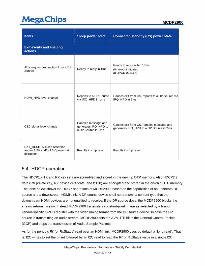
5.3. Power management .......................................................................................................................... 19
5.4. HDCP operation ................................................................................................................................ 20
5.5. CEC tunneling over AUX ................................................................................................................... 21
6. System interface ....................................................................................................................................... 22
6.1. I2C interface ...................................................................................................................................... 22
6.2. SPI interface ...................................................................................................................................... 22
6.3. UART interface .................................................................................................................................. 22
6.4. GPIO interface .................................................................................................................................. 23
6.5. Locking of system interfaces ............................................................................................................. 23
6.6. Development Parts with FX marking ................................................................................................. 23
7. BGA footprints and pin list ........................................................................................................................ 24
7.1. Signal mapping sorted by ball (pin) number ..................................................................................... 25
8. Connections.............................................................................................................................................. 28
8.1. Pin list ................................................................................................................................................ 28
8.2. Bootstrap configuration ..................................................................................................................... 32
8.3. EXT_RESETN connection ................................................................................................................ 32
9. Package .................................................................................................................................................... 34
9.1. Package drawing ............................................................................................................................... 34
9.2. LFBGA 7 x 7 dimensions .................................................................................................................. 35
9.4. Marking field template and descriptors ............................................................................................. 36
9.5. Classification reflow profile................................................................................................................ 36
10. Electrical specifications ......................................................................................................................... 37
10.1. Absolute maximum ratings ............................................................................................................ 37
10.2. Power connections ........................................................................................................................ 38

MCDP2900
MegaChips’ Proprietary Information – Strictly Confidential
Page 4 of 48
10.3. DC characteristics ......................................................................................................................... 39
10.4. AC characteristics .......................................................................................................................... 41
10.4.1. DisplayPort receiver ............................................................................................................... 41
10.4.2. HDMI transmitter I/O specifications ........................................................................................ 42
10.4.3. I2C interface timing ................................................................................................................ 43
10.4.4. SPI interface timing ................................................................................................................ 45
11. Ordering information ............................................................................................................................. 46
12. Revision history .................................................................................................................................... 47

MCDP2900
MegaChips’ Proprietary Information – Strictly Confidential
Page 5 of 48
List of tables Table 1. Crystal specifications ..................................................................................................................... 17
Table 2. MCDP2900 power saving states ................................................................................................... 19
Table 3. HDCP operations of MCDP2900 ................................................................................................... 21
Table 4. Pin list ............................................................................................................................................ 25 Table 5. DisplayPort receiver pins ............................................................................................................... 28
Table 6. HDMI output pins ........................................................................................................................... 29
Table 7. System interface pins .................................................................................................................... 30
Table 8. Power and ground pins.................................................................................................................. 31
Table 9. Bootstrap configuration.................................................................................................................. 32 Table 10. MCDP2900 package dimensions .............................................................................................. 35
Table 11. Field descriptors ......................................................................................................................... 36
Table 12. Absolute maximum ratings ........................................................................................................ 37
Table 13. DC characteristics ...................................................................................................................... 39
Table 14. IO DC characteristics ................................................................................................................. 40
Table 15. Maximum speed of operation .................................................................................................... 41 Table 15. DisplayPort receiver characteristics ........................................................................................... 41
Table 16. HDMI transmitter DC specifications ........................................................................................... 42
Table 17. HDMI transmitter AC characteristics .......................................................................................... 43
Table 18. I2C interface timing .................................................................................................................... 43
Table 19. SPI interface timing .................................................................................................................... 45
Table 20. Order codes ............................................................................................................................... 46 Table 21. Document revision history ......................................................................................................... 47

MCDP2900
MegaChips’ Proprietary Information – Strictly Confidential
Page 6 of 48
List of figures Figure 1. MCDP2900 block diagram ........................................................................................................... 8
Figure 2. MCDP2900 adaptor (dongle) use case ..................................................................................... 10
Figure 3. MCDP2900 block diagram ......................................................................................................... 11
Figure 4. Power-up timing sequence ........................................................................................................ 15 Figure 5. Internal crystal oscillator operation ............................................................................................ 16
Figure 6. Parasitic capacitance sources ................................................................................................... 17
Figure 7. MCDP2900 BGA diagram .......................................................................................................... 24
Figure 8. EXT_RESETN Connection to MCDP2900 ................................................................................ 33
Figure 9. MCDP2900 package drawing .................................................................................................... 34 Figure 10. Marking template ....................................................................................................................... 36
Figure 11. Recommended Power supply connections for MCDP2900....................................................... 38
Figure 12. I2C timing ................................................................................................................................... 44

MCDP2900
MegaChips’ Proprietary Information – Strictly Confidential
Page 7 of 48
Features • DisplayPort® (DP) ver. 1.4 receiver
− Up to 5.4Gbps Link rate supporting HBR2/HBR/RBR modes
− 1, 2, or 4 lanes configuration − Programmable receiver equalization − Single Stream − AUX CH 1 Mbps − 3.3V HPD_OUT − Link Training (LT) enhancements as in
DP1.4 specification − Video Stream Handling
− Up to 600MHz dual pixel path and 16bpc
− RGB/ YCbCr 444/422/420 pixel format
− Horizontal expansion of VESA CVT to CEA timings as per DP1.4 specification
− DPCD and CEC − Supports DPCD data structure
revision 1.4 as per DP1.4 specification
− Supports CEC tunneling over AUX − DP to HDMI Stereoscopic 3D Transport
− Frame Sequential to Stacked Top-Bottom Conversion
− Pass-through of other 3D formats − Audio Stream handling
− LPCM and Compressed Audio encoding formats
− Max Audio sample rate of 192KHz x8 Channel or 768KHz x2 Channel
• HDMI ver. 2.0a transmitter
− 600 MHz maximum TMDS character clock
− DC-coupled outputs with source termination
− TMDS character-clock divide_by_4 Mode − Scrambling over HDMI2.0a − Programmable edge rate control − Programmable pre-emphasis control − Deep color up to 16 bits per color
− High Dynamic Range support (Static and Dynamic HDR)
− 3D video timings − CEC support – snooping, tunneling − HPD_IN handling − SCDC read request handling
− Polling enabled for HDMI sinks not supporting read requests
• Video Input Processing (up to 6Gbps)
− Color space conversion − 10 bits per color input width − 12 bits per color output width − 16 bits per color pass through − Programmable coefficient 3x3 matrix − Programmable input offset − Programmable output offset − Programmable output clipping levels
• Chroma Down Sampling
− 5-tap H & V FIR filters with programmable coefficients
− 12 bits per color input width − 12 bits per color output width − YCbCr444 to YCbCr420 conversion − YCbCr444 to YCbCr422 conversion − YCbCr422 to YCbCr420 conversion − Bypass chroma down-sampling for
YCbCr420 input over DP Link
• Max video resolution and color depth on HDMI TX output
− 4Kp60Hz, RGB/YCbCr444, 8 bpc − 4Kp60Hz, YCbCr422 up to 12 bpc − 4Kp60Hz, YCbCr420, up to 16 bpc − 4Kp30Hz, RGB/YCbCr444, up to 16 bpc
• Audio stream forwarding from DP RX to HDMI TX
− Up to 8-ch, 192 kHz, 24 bps LPCM audio, AC3, DTS, Dolby-HD
− 2-ch, 768 kHz 24 bps HBR audio
• HDCP support
− HDCP1.3 to HDCP1.4 Repeater function − HDCP2.2 to HDCP1.4 Repeater function

MCDP2900
MegaChips’ Proprietary Information – Strictly Confidential
Page 8 of 48
− HDCP2.2 to HDCP2.2 Repeater function − Read-protected embedded HDCP keys
• Enhanced security
− Encrypted on-chip key storage − Security signed application firmware − Secure boot-up procedure − Debug ports disabled in production
• Metadata handling
− HDMI TX DVI/HDMI mode setting (DPCD register)
− YCbCr444-420 conversion (DPCD register)
− IEC60958 BYTE3 Channel Status overwrite
− CEA861F INFOFRAME generation − CEA861.3 HDR and Mastering InfoFrame
as per DP1.4 specification
• Device configuration options
− 8Mbit SPI flash for firmware binary image storage
− AUX CH, I2C host interface
• Internal video pattern generator
− Configurable through DPCD registers
• EMI reduction support
− Spread spectrum for DP input − Scrambler for DP input and HDMI2.0a
output
• Low power operation
− 570 mW in protocol converter operation − 11 mW sleep mode operation − 4 mW in Connected Standby operation
• ESD specification
− ESD: +/-2 KV HBM, 500 V CDM − ESD: +/-6.5 KV HBM connector facing
pins
• Package
− 64 LFBGA (7 x 7 mm)
• Power supply voltages
− 3.3 V I/O; 1.2 V core
Applications • Notebook, Tablet Accessories (USB Type-C
dongles, docking stations)
• TV, Signage, Game consoles, STB
Figure 1. MCDP2900 block diagram
HPD_OUTDPRX_HPD_OUT
AUX
DP1.3 Receiver
DP to HDMI AV Format Converter
HDCP Repeater
OCMV186
DPRX_AUX_P/_NDPRX_L0_P/_NDPRX_L1_P/_NDPRX_L2_P/_NDPRX_L3_P/_N
Clock Generation
XTAL
EXT_RESETN Reset Generation
TCLK
GPIO I2C_SDAGPIO2_33
CEC
HDMI2.0a Transmitter
I2C Slave
UART UART_RXUART_TX
I2C_SCL
HDMITX_CEC
HPD_IN HDMITX_HPD_IN
HDMITX_DDC_SDAI2C Slave HDMITX_DDC_SCA
HDMITX_CH0_P /_NHDMITX_CH1_P /_NHDMITX_CH2_P /_N
HDMITX_CLK_P /_N
GPIO1_33
SPI
VDD12ONVDD12_ON
SPI_DISPI_DOSPI_CLKSPI_CSSPI_WPN

MCDP2900
MegaChips’ Proprietary Information – Strictly Confidential
Page 9 of 48
1. Description The MCDP2900 is a power-optimized DisplayPort1.4-to-HDMI2.0a converter, targeted for enabling USB
Type-C DP Alt mode on TVs, Game consoles and other consumer equipment as well as for mobile PC and
tablet accessory applications. This device functions as an active protocol converter with HDCP1.x/ HDCP2.2
repeater supporting HDR video quality for deep color media content playback.
MCDP2900 behaves as a DP branch device with a DP-to-HDMI transport protocol converter function and
allows a DP or USB Type-C source to drive an HDMI2.0a sink device. The maximum TMDS character clock
frequency supported is 600 Mchar/s (per HDMI2.0a specification).
The MCDP2900 operates with two power supply voltages: 1.2 V and 3.3 V. It consumes:
• 570 mW in protocol converter operation
• 11 mW sleep mode operation
• 4 mW in connected standby mode operation
The MCDP2900 has a DP1.4 receiver and an HDMI2.0a transmitter. The DP receiver supports up to
5.4Gbps/lane over 4 lanes. It supports DP SST transport format on its main link and Manchester-coded AUX
signaling as the side band channel. The downstream HDMI TX port is HDMI2.0a specification compliant.
The MCDP2900 is capable of supporting Ultra High-Definition video formats with resolutions as high as 4096
x 2160 progressive @ 60 Hz (4K2Kp60Hz). It supports RGB/YCbCr video color formats with a color depth of
16 bpc (bits per component or 48 bits per pixel) as long as it fits within the DP and HDMI link bandwidth. This
device also supports pixel encoding conversion from RGB or YCbCr444 to YCbCr420 and a YcbCr420 pass-
through function. In addition, High Dynamic Range (HDR) with deep color up to 12bpc at 4Kp60Hz is
supported through the conversion of RGB/YCbCr444 over DP link to YCbCr420 on the HDMI output with a
horizontal expansion to CEA timings.
This device offers secure reception and transmission of high bandwidth digital audio and video content with
HDCP1.3 and HDCP2.2 content protection for the upstream DP interface. It also has a repeater function for
HDCP1.4 and HDCP2.2 for the downstream HDMI interface.
The MCDP2900 uses an external crystal of 27 MHz as a reference clock for its operation. An internal Power
On Reset (POR) circuit senses the voltage on the reset input and provides the chip reset during system
power-up. The device has an internal microcontroller with SPI, UART (debug only), and I2C system interface
signals. It uses an external 8Mbit SPI flash memory for storing a secure signed firmware image with fail-safe
recovery. Firmware updates of the SPI flash are done securely through the DP AUX_CH or I2C, depending
on the application.

MCDP2900
MegaChips’ Proprietary Information – Strictly Confidential
Page 10 of 48
2. Application overview The target applications of MCDP2900 are the notebook, tablet accessories i.e., adaptors (dongles), docking
stations and other AV accessories. MCDP2900 is also intended for enabling USB Type-C DP alternative
mode for inside-the-box applications such as TVs, game consoles and other consumer equipment.
2.1. Adaptor application
In a dongle topology the MCDP2900 is part of the source side adaptor that plugs into a DP source device via
a DisplayPort connector (e.g. full-size DP or mini-DP receptacle or USB-Type-C Alt-Mode receptacle on the
upstream facing port). In the conventional DP-to-HDMI dongle application, MCDP2900 functions as a system
master and operates as a protocol converter, an HDCP1.x repeater or an HDCP2.2 repeater. In a Type-C
dongle design, a PD controller functions as the system master. The upstream source typically powers the
dongle.
Figure 2. MCDP2900 adaptor (dongle) use case
DongleSource SoC
MCDP2900 HDMI SinkHDMI Cable
2.2. Docking station application
In a docking station topology, the MCDP2900 is part of a larger system into which a DP source device plugs
in via a custom connector or USB-Type-C Alt-Mode receptacle on the upstream facing port. In a docking
station design the MCDP2900 typically co-exists with other system components such as the system host or
PD controller, AV switch, and USB hub. In this application, the MCDP2900 functions as a protocol converter,
an HDCP1.x repeater, or an HDCP2.2 repeater.
Source SoC
MCDP2900
HDMI SinkHDMI Cable
Host /PD Controller
USBHub
Switch /
De-M
ux
DP SinkDP Cable

MCDP2900
MegaChips’ Proprietary Information – Strictly Confidential
Page 11 of 48
2.3. TV Application
A TV system featuring the USB Type-C connector supporting the DP Alt-mode requires a DP-to-HDMI
protocol converter. The MCDP2900 is an ideal fit for such applications; it supports video resolution up to
4K60Hz with HDR video quality for deep color media playback, end-to-end HDCP2.2 content protection, and
CEC tunneling over DP for single-point remote-control access for all connected devices.
3. System block diagram Figure 3. MCDP2900 block diagram
DPRX_HPD_OUT
SPI BUS
I2C_SDA
EXT_RESETN
MCDP2900
SPI FLASH 8Mbit
SPI_
CSN
SPI_
DOSP
I_SC
KSP
I_W
PSP
I_DI
I2C_SCL
XTLI
XTLO
RX_L3_P
RX_L2_PRX_L2_N
RX_L1_PRX_L1_N
RX_L0_PRX_L0_N
RX_L3_N
1.2V1.2V
HDMI_RX_HPD_OUTHDMI_TX_CH2P
HDMITX_HPD_INHDMI_RX_CH2_P
HDM
I CO
NN
HDMI_5V
HDMI_TX_CH2N HDMI_RX_CH2_NHDMI_TX_CH1P HDMI_RX_CH1_PHDMI_TX_CH1N HDMI_RX_CH1_NHDMI_TX_CH0P HDMI_RX_CH0_PHDMI_TX_CH0N HDMI_RX_CH0_NHDMI_TX_CLKP HDMI_RX_CLK_PHDMI_TX_CLKN HDMI_RX_CLK_N
3.3V27MHz
DP_TX_L3_P
DP_HPD_INDP_TX_L3_N
DP_TX_L2_PDP_TX_L2_N
DP_TX_L1_PDP_TX_L1_N
DP_TX_L0_PDP_TX_L0_N
3.3V SPI INTERFACE
3.3V-5V DC-DC CONV
1.2V LDO REG
DP_TX_AUX_P DP0_AUXP
HOST 3V3
HDMI Sink
DP_TX_AUX_N DP0_AUXN
1V2
VDD33_x VDD12_xVDD12ON
CEXTREXT1V2
DISP
LAYP
ORT
CO
NN
DP Source
1314
GPIO1GPIO2 HDMI_CECHDMI_CEC
HDMI_SCL
HDMI_SDA
5V
5V
3.3V
HDMI_RX_SDA
HDMI_RX_SCL
UART_RXUART_TX
DEBUG PORT
3V3
LDO Control is optional
TV SystemMobile PC / CE Source
CPU /Source SoC
MCDP2900
USB Type-C cableTV SoC
Sw
itch /D
e-Mux
I2C
USB
DP HDMI
MCDP2900
MegaChips’ Proprietary Information – Strictly Confidential
Page 12 of 48
4. Interface description
4.1. Input interface
The MCDP2900 receives audio-video streams from a source device via the DP1.4 link supporting a main link
configuration of up to 4 lanes (and up to 5.4Gbps/lane) with 0.5% down-spread option. The DP link consists
of 4 main lanes, AUX CH, and a DP_HPD signal.
Both the main link receiver and AUX CH transceiver are internally terminated to the 1.2 V power rail. The
AC-coupling capacitors for the AUX signals shall be placed externally. The DP_HPD signal is a 3.3V TTL
signal set to “1” when MCDP2900 is ready to handle an AUX request transaction. An external pull down
resistor of 100 Kohm shall be used. The power for MCDP2900 can be provided by a DP source device,
DP_PWR on a DP connector, or from the USB Type-C connector, or by an external supply.
MCDP2900 supports both native AUX transaction syntax and I2C-over-AUX transaction syntax. With I2C-
over-AUX transactions, a DP source can access the downstream EDID. EDID larger than 256 bytes can be
accessed by using segmented addressing mechanism specified in the E-DDC standard.
The MCDP2900 supports link training with AUX transactions as specified in DP1.4. The usage of TPS4
(Training Pattern Sequence 4) added to DP1.4 is recommended to optimize both DPTX PHY drive setting of
DP source and its own DPRX EQ setting. If a DP source does not support TPS4, support of the
POST_LT_ADJ_REQ procedure as defined in DP1.4 is recommended. Once the DP source has performed
link training, but later stops the main link signal transmission (for example, transitioning to the power saving
state with DPCD 00600h set to 02h), MCDP2900 requires another full link training to re-establish the link.
MCDP2900 also supports the new link training policy defined for DP alternative mode sources. In this policy,
the lane count is reduced to match the number of lanes physically connected based on the DPCD clock
recovery status register [LANEx-CR_DONE].
By default, the firmware keeps DP_HPD asserted unless it is in OFF power state, regardless of whether
HDMI_HPD input is asserted or not. The HDMITX_HPD input status is reflected on SINK_COUNT value at
DPCD 00200h. The value is 1 when the HDMITX_HPD input is asserted, and 0 when de-asserted.
Whenever MCDP2900 detects HDMI_HPD input status change, it generates IRQ_HPD on the DP_HPD line.
4.1.1. Video stream regeneration
The MCDP2900 is capable of regenerating an incoming video stream from a DP source up to
600Mpixels/sec and 16 bits per component / 48 bits per pixel, as long as the video stream bandwidth fits
within the link bandwidth.

MCDP2900
MegaChips’ Proprietary Information – Strictly Confidential
Page 13 of 48
4.1.2. Horizontal blanking expansion
MCDP2900 supports VESA CVT horizontal reduced blanking to CEA-861-F conversion up to 4Kp60Hz video
timing format.
4.1.3. On-chip video pattern generation
MCDP2900 has an on-chip pattern generator controlled by vendor-specific DPCD Addresses 00579h ~
0057Bh.
4.1.4. Audio stream regeneration
The DP receiver is capable of regenerating 2-ch audio up to 768 kHz, and 8-ch audio up to 192 kHz, with the
sample bit depth of 16, 20, and 24 bits per sample.
4.1.5. HDCP RX
MCDP2900 supports HDCP1.3 and HDCP2.2 for DP. The HDCP RX key sets are stored in a secure on-chip
OTP memory.
4.2. Output interface
The MCDP2900 outputs audio-video streams in DC-coupled (3.3 V level) TMDS format to the downstream
HDMI connector. The HDMI transmitter in MCDP2900 is compliant with both HDMI1.4 and HDMI2.0a
specifications.
4.2.1. HDMI transmitter
The HDMI output port consists of 3 data pairs, a clock pair, a DDC channel, HDMI_HPD signal and CEC
signal. The maximum data rate on this link is 6.0 Gbs per channel. Both data and clock channels shall be
terminated to 3.3 V by the downstream HDMI receiver. MCDP2900 autonomously controls both TMDS
character clock divide by 4 and scrambling as defined by HDMI2.0a. Differential voltage swing, pre-
emphasis, edge rate, and source termination can be controlled by vendor-specific DPCD registers.
The HDMI TX PHY is capable of generating three PHY test patterns selectable by DPCD registers.
The HDMI_HPD input signal shall be directly connected to the downstream HDMI_HPD from the HDMI
connector.

MCDP2900
MegaChips’ Proprietary Information – Strictly Confidential
Page 14 of 48
The HDMI CEC feature is supported by MCDP2900 as defined in the DP1.4 specification. CEC commands
between downstream HDMI device and upstream DP source device are tunneled through DP AUX_CH.
4.2.2. HDCP TX
MCDP2900 supports HDCP1.4 and HDCP2.2 content protection. It functions as an HDCP1.x and HDCP2.2
repeater. The HDCP key sets are stored in a secure on-chip OTP memory.
4.2.3. DDC master
The HDMI TX has a DDC master that supports EDID reads, MCCS and SCDC read requests. The DDC
channel is a 5 V, open-drain signal; it requires an external diode termination with a 2.2 KΩ series resistor to
a 5 V supply. No more than 10 uA of current per DDC pad is drawn when the DDC lines are pulled up to
5.5 V while the chip is powered off. The DDC data rate is selected in the range of 1 kbps to 100 kbps, with
50 kbps being the default rate, by DPCD address 00109h.
MCDP2900 reads the HDMI RX link error status once every 100 ms and updates the HDMI link error status
registers at DPCD 03031h ~ 03033h. An IRQ_HPD is generated with any HDMI_LINK_STATUS_CHANGE.
4.2.4. HDMITX_HPD
MCDP2900 monitors the HDMI_HPD status unless it is in the OFF power state and updates the
SINK_COUNT DPCD register value at DPCD Address 00200h. The value is 1 when HDMI_HPD is asserted
and 0 when HDMI_HPD is de-asserted. Upon the HDMI_HPD status change, the chip generates an
IRQ_HPD on DP_HPD line with the SINK_COUNT value updated.
HDMITX_HPD_IN pin shall have a 20k pull-down resistor. No more than 10 uA of current pad is drawn by
HDMITX_HPD_IN pin when it is pulled up by the sink to 5.5 V while the chip is powered off.
4.2.5. CEC
The MCDP2900 supports tunneling CEC commands as defined in the DP1.4 specifications. In addition, CEC
snooping and multiple logical address capability are supported. The CEC pin is connected to a 3.3 V open
drain pad. No more than 10 uA of pad current is drawn while the chip is powered off.
4.3. Chip power-up sequence and reset
The figure below shows the power-up timing sequence requirements of the 3.3 V and 1.2 V power rails and
the internal reset signal.

MCDP2900
MegaChips’ Proprietary Information – Strictly Confidential
Page 15 of 48
During rail power up, the voltage (pull-up resistor to 3.3 V supply) on EXT_RESETN pin is sensed by the
internal Power-On Reset (POR) circuit to generate an internal reset pulse. Additionally, MCDP2900 also sets
a VDD12ON signal that can be used to optionally control the external 1.2 V regulator that supplies the 1.2 V
power rail. The internal reset pulse is low until both the 3.3 V and 1.2 V rails are stable. The internal reset
pulse continues to stay low for at least 1 ms after the 1.2 V power rail reaches 0.8 V. During the device
power up, the 3.3 V supply shall lead the 1.2 V supply (VDD33 >= VDD12 for t > 0).
Figure 4. Power-up timing sequence
Vol
tage
Time
VDD33
VDD12 controlled with VDD12_ON
t
At any time: VDD33 >= VDD12
VDD12_ON (follows VDD33)
0.8V
1.5 ms (typ)
INTERNAL_RESETn(dotted line)
> 0.2ms 1.5ms (typ)
EXT_RESETn pulled low by a system host for 0.2 ms
EXT_RESETn kept low by INTERNAL_RESETn after a narrow glitch (~ 25ns)
Any time a power supply glitch causes the power rails to fall below 2.7 V (for 3.3 V power rail) and below 0.8
V (for 1.2 V power rail), the internal reset signal drops and stays low for at least 1 ms after the 1.2 V power
rail reaches 0.8 V again.
An external reset signal (active low) can be applied to the EXT_RESETN pin. This shall be driven by an
Open-Drain Output.
4.4. Clock generation
The 27 MHz TCLK is the main timing clock for this device. All other internal clocks are generated from the
TCLK. The internal TCLK oscillator generates TCLK when a crystal is attached as shown in the figure below.

MCDP2900
MegaChips’ Proprietary Information – Strictly Confidential
Page 16 of 48
Figure 5. Internal crystal oscillator operation
AVDD12
C1=22pF
C2=22pF
TCLK
XTAL
27 MHz
4.4.1. Internal crystal oscillator operation
A crystal is connected between the XTAL pin and the TCLK pin with the external capacitors (C1 and C2)
to match the proper value of loading capacitance specified in crystal specification. The logic level on the
SPI_CSN pin is latched during the de-asserting edge of the RESETN signal and provides the
XTAL_OSC_SEL bootstrap signal. A ‘1’ latched on this pin enables the crystal and internal oscillator. A ‘0’
latched on this pin turns off the internal oscillator thus enables the use of an external oscillator on the TCLK
pin.
Note: The value of C1 and C2 are determined based on the loading capacitance from the crystal specification and by compensating for the parasitic capacitance of the device and the printed circuit board traces. The external capacitors are terminated to the Analog 1V2 power supply. This connection increases the power supply rejection ratio when compared to terminating the loading capacitors to ground.
The external capacitors' value used with the crystal (shown below) is an important design parameter. The
loading capacitance (Cload) on the crystal is the combination of C1 and C2 and is calculated by Cload =
((C1 * C2)/(C1 + C2)) + Cshunt+Cparasitic. The shunt capacitance Cshunt is the effective capacitance
between the XTAL and TCLK pins. Refer to crystal specification for the proper Cshunt value. The
Parasitic capacitance is the combination of the PCB board capacitance (Cpcb), the pin capacitance (Cpin),
the pad capacitance (Cpad), and the ESD protection capacitance (Cesd). The overall parasitic
capacitance is 2-3pF range for MCDP2900 design.

MCDP2900
MegaChips’ Proprietary Information – Strictly Confidential
Page 17 of 48
Figure 6. Parasitic capacitance sources
XTAL
TCLK
MCDP2900
C1
C2
Internal Oscillator
Cpcb
Cshunt
Cpcb Cpin Cpad Cesd
Cpin Cpad Cesd
AVDD12
27 MHz
Cparasitic ~2-3pF (layout dependent)
AVDD12
Note these details of the oscillator circuit when used with a crystal resonator:
• The PCB traces should be as short as possible.
• The crystal should be a parallel resonate-cut
4.4.2. Crystal specifications
While the selection of a crystal mainly depends on the specific PCB layout and the crystal manufacturer's
specifications, the following are general recommendations.
Table 1. Crystal specifications
Parameters Specifications
Frequency 27.000 MHz
Operation Mode Fundamental
Operating Temperature -10 ºC to +70 ºC
Frequency Tolerance @ 25oC +/- 50 ppm max

MCDP2900
MegaChips’ Proprietary Information – Strictly Confidential
Page 18 of 48
5. Chip operation
5.1. Initial state
Upon power-up or after reset, the MCDP2900 executes a secure boot from IROM based firmware code.
After initial system setup and configuration, the IROM firmware performs validation of the code image stored
in the external SPI flash memory and copies this into internal memory. Upon successful validation, the code
executes from the internal memory. For security reasons further access to the external SPI-Flash memory is
blocked. If code image validation fails, execution from IROM continues in a tight loop until reset or power off.
5.2. Video pixel processing
MCDP2900 embeds a video pixel converter which is capable of color space conversion and horizontal and
vertical chroma down sampling.
5.2.1. Color Space Converter
The Color Space Converter block receives 10 bits per component from the DPRX or on-chip video pattern
generator, and outputs12 bits per component.
12-bit output is 12.0, 10.2, or 8.4. The 12.0 bit data can be generated by the 3x3 matrix in the Color Space
Converter block: 10 integer bits plus 2 zero-padding (or most significant 2 bits padding), or 8 integer bits plus
4 zero-padding bits. This block is controlled by vendor-specific DPCD registers.
5.2.2. Horizontal Chroma Down-Sampler
Horizontal Chroma Down-Sampler receives 12 bits per component from CSC block and outputs 12 bits per
component. 12-bit output is 12.0, 10.2, or 8.4.
This block is controlled by Horizontal Chroma Down-Sampler control register at DPCD 0057Fh and DPCD
005ACh ~ 005B5h for 5-tap coefficients.
5.2.3. Vertical Chroma Down-Sampler
Vertical Chroma Down-Sampler receives 12 bits per component either from CSC block or from Horizontal
Chroma Down-Sampler, and outputs 12 bits per component. 12-bit output is 12.0, 10.2, or 8.4.
This function is controlled by Vertical Chroma Down-Sampler control at DPCD 00580h, and DPCD 005B6h ~
005BFh for 5-tap coefficients.

MCDP2900
MegaChips’ Proprietary Information – Strictly Confidential
Page 19 of 48
5.3. Power management
The MCDP2900 uses 3.3 V and 1.2 V power supplies. In a dongle application, MCDP2900 receives the 3.3V
power supply from the DP source. The 1.2 V supply is generated from 3.3 V using an on-board 1.2 V (LDO
or SMPS) regulator. In other applications the 3.3V and 1.2V are supplied by the on system PMIC. The DP
source puts MCDP2900 into a low power state writing 02h to DPCD 00600h. An alternative connected
standby power state can be activated when a DP source grants the extended DPRX sleep wakeup time out.
In this power state, all internal PLL and clock sources are either turned off or run at a reduced frequency.
Additionally, Analog blocks are also put to low power mode operation or disabled.
Table 2. MCDP2900 power saving states
Items Sleep power state Connected standby (CS) power state
Register setting
EXTENDED_DPRX_SLEEP_WAKE_TIMEOUT_GRANT DPCD register setting (at DPCD Address 00119h)
00h 01h
Conditions in the power saving state
Power consumption 20mW typical 4 mW typical
TCLK Remains running Disabled
DP_HPD Remains asserted Remains asserted
GPIO’s Retain states Retain states
Registers Retains states Retain states
AUX request transaction Monitored Monitored
HDMI_HPD Monitored Monitored
CEC Monitored Monitored
Entry
Trigger event DPCD 00600h = 02h DPCD 00600h = 02h
MCDP2900
MegaChips’ Proprietary Information – Strictly Confidential
Page 20 of 48
Items Sleep power state Connected standby (CS) power state
Exit events and ensuing actions
AUX request transaction from a DP Source Ready to reply in 1ms
Ready to reply within 10ms (time-out indicated at DPCD 02211h)
HDMI_HPD level change Reports to a DP Source via IRQ_HPD in 1ms
Causes exit from CS, reports to a DP Source via IRQ_HPD in 2ms
CEC signal level change Handles message and generates IRQ_HPD to a DP Source in 1ms
Causes exit from CS, handles message and generates IRQ_HPD to a DP Source in 2ms
EXT_RESETN pulse assertion and/or 1.2V and/or3.3V power rail disruption
Results in chip reset Results in chip reset
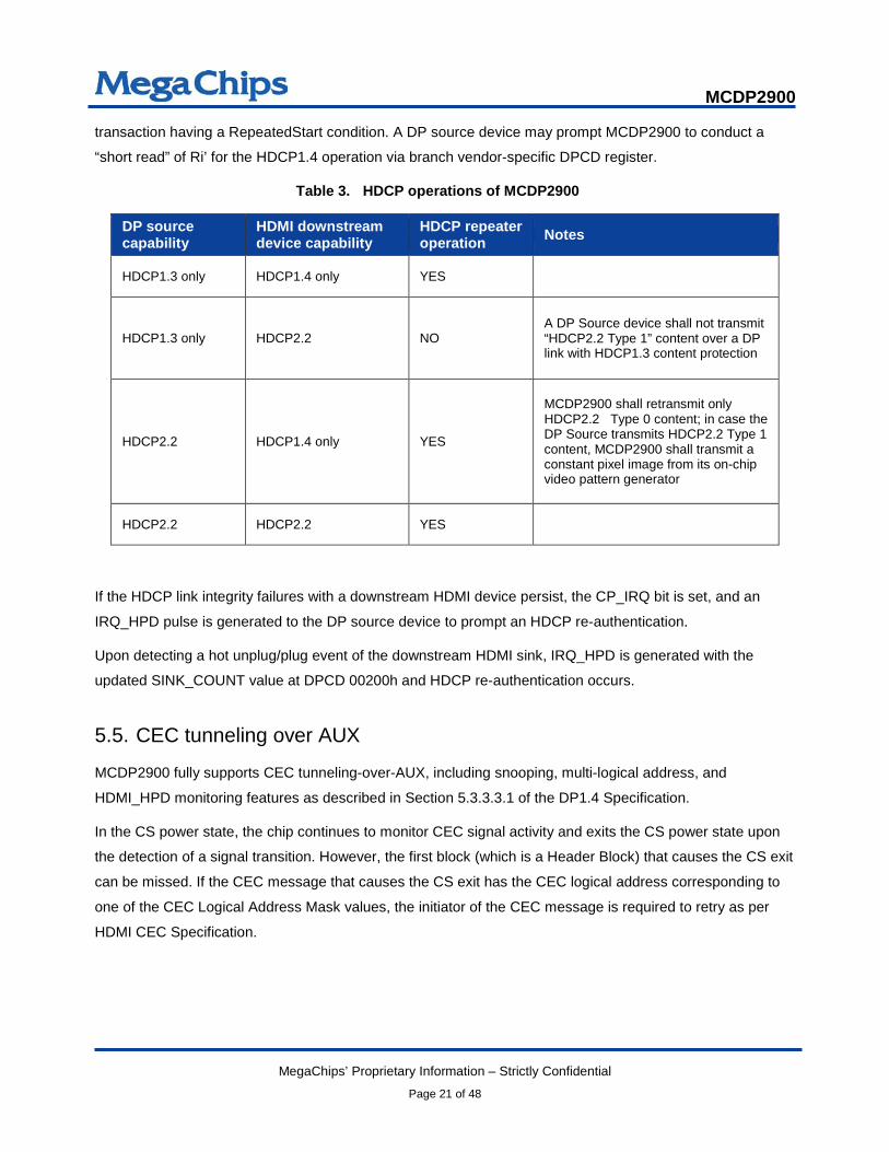
5.4. HDCP operation
The HDCP1.x TX and RX key sets are scrambled and stored in the on-chip OTP memory. Also HDCP2.2
data (RX private key, RX device certificate, and lc128) are encrypted and stored in the on-chip OTP memory.
The table below shows the HDCP operations of MCDP2900, based on the capabilities of an upstream DP
source and a downstream HDMI sink. A DP source device shall not transmit a content type that the
downstream HDMI devices are not qualified to receive. If the DP source does, the MCDP2900 blocks the
stream retransmission. Instead MCDP2900 transmits a constant-pixel image as selected by a branch
vendor-specific DPCD register with the video timing format from the DP source device. In case the DP
source is transmitting an audio stream, MCDP2900 sets the AVMUTE bit in the General Control Packet
(GCP) and stops the transmission of Audio Sample Packets.
As for the periodic Ri’ (or RxStatus) read over an HDMI link, MCDP2900 uses by default a “long read”. That
is, I2C writes to set the offset followed by an I2C read to read the Ri’ or RxStatus value in a single I2C
MCDP2900
MegaChips’ Proprietary Information – Strictly Confidential
Page 21 of 48
transaction having a RepeatedStart condition. A DP source device may prompt MCDP2900 to conduct a
“short read” of Ri’ for the HDCP1.4 operation via branch vendor-specific DPCD register.
Table 3. HDCP operations of MCDP2900
DP source capability
HDMI downstream device capability
HDCP repeater operation Notes
HDCP1.3 only HDCP1.4 only YES
HDCP1.3 only HDCP2.2 NO A DP Source device shall not transmit “HDCP2.2 Type 1” content over a DP link with HDCP1.3 content protection
HDCP2.2 HDCP1.4 only YES
MCDP2900 shall retransmit only HDCP2.2 Type 0 content; in case the DP Source transmits HDCP2.2 Type 1 content, MCDP2900 shall transmit a constant pixel image from its on-chip video pattern generator
HDCP2.2 HDCP2.2 YES
If the HDCP link integrity failures with a downstream HDMI device persist, the CP_IRQ bit is set, and an
IRQ_HPD pulse is generated to the DP source device to prompt an HDCP re-authentication.
Upon detecting a hot unplug/plug event of the downstream HDMI sink, IRQ_HPD is generated with the
updated SINK_COUNT value at DPCD 00200h and HDCP re-authentication occurs.
5.5. CEC tunneling over AUX
MCDP2900 fully supports CEC tunneling-over-AUX, including snooping, multi-logical address, and
HDMI_HPD monitoring features as described in Section 5.3.3.3.1 of the DP1.4 Specification.
In the CS power state, the chip continues to monitor CEC signal activity and exits the CS power state upon
the detection of a signal transition. However, the first block (which is a Header Block) that causes the CS exit
can be missed. If the CEC message that causes the CS exit has the CEC logical address corresponding to
one of the CEC Logical Address Mask values, the initiator of the CEC message is required to retry as per
HDMI CEC Specification.

MCDP2900
MegaChips’ Proprietary Information – Strictly Confidential
Page 22 of 48
6. System interface The MCDP2900 has the following system interfaces:
• I2C slave interface
• SPI interface
• UART interface
6.1. I2C interface
The I2C slave interface is intended for an external host controller to configure the MCDP2900 registers in
certain use cases as needed. For example in a type-C docking station the host controller may use this
interface to check the MCDP2900 power-ON status and for downloading firmware etc. However, this
interface is not enabled in the current application firmware.
6.2. SPI interface
The MCDP2900 has an SPI interface for connecting external program flash memory (SPI Flash device). The
maximum clock rate for the SPI interface is 50 MHz. The required SPI Flash ROM size is 8 MBits for storing
the application firmware code image with dual-bank option for fail-safe. The SPI flash is programmed via the
DisplayPort AUX interface. MegaChips provides the In-system-Programming (ISP) tool and the driver for
programming the SPI flash ROM. Contact MegaChips for the list of SPI flash devices supported in the ISP
driver. The SPI interface between MCDP2900 and a serial flash ROM is as follows. All signals of the SPI
interface are LVTTL (3.3 V):
• SPI_CSN: SPI chip select, connect to CE# of SPI flash ROM
• SPI_WP: SPI write protect, connect to WP# of SPI flash ROM
• SPI_DO: SPI data output from MCDP29x0, connect to SPI_DI of SPI flash ROM
• SPI_DI: SPI data input to MCDP29x0, connect to SPI_DO of SPI flash ROM
• SPI_CLK: SPI clock signal, connect to SPI_SCK of the SPI flash ROM
6.3. UART interface
The UART interface is used only during product development for firmware programming, testing, and
debugging purpose. For security reasons, the UART interface is blocked in the production version of the
silicon. All UART signals are LVTTL (3.3 V) level. The UART interface supports a maximum baud rate of
115k-baud.

MCDP2900
MegaChips’ Proprietary Information – Strictly Confidential
Page 23 of 48
6.4. GPIO interface
The GPIO interface consists of 4 pins (GPIO1_33, GPIO2_33, I2C_SDA, I2C_SCL) which may be
configured and used by application firmware.
6.5. Locking of system interfaces
MCDP2900 hardware locks the UART interface for enhanced security. Also the SPI interface is locked after
successful completion of the secure boot up.
6.6. Development Parts with FX marking
A special type of MCDP2900 FX is available for development purposes. These parts are programmed with
HDCP facsimile keys and have none of the interfaces locked.

MCDP2900
MegaChips’ Proprietary Information – Strictly Confidential
Page 24 of 48
7. BGA footprints and pin list The ball grid array (BGA) diagrams give the allocation of pins to the package, shown from the top looking
down using the PCB footprint.
Some signal names in BGA diagrams have been abbreviated. Refer to the pin list for full signal names
sorted by pin number.
Figure 7. MCDP2900 BGA diagram
A
B
C
D
E
F
G
H
1 2 3 4 5 6 7 8
1 2 3 4 5 6 7 8
A
B
C
D
E
F
G
H
DPRX_L3N DPRX_L3P
DPRX_HPD_OUT
VDD33_RX GND VDD12_
RXVDD12_
RX GND VDD12_PLL
EXT_RESETN
SPI_CSN SPI_DI GPIO1_33VDD33_
RXVDD33_
AUX R_EXT DPRX_AUXP
DPRX_AUXN
SPI_DO SPI_CLK VDD33_IO GND GND VDD12_
DIG UART_TX GND
HDMITX_DDC_SCL SPI_WPN VDD33_
IO GND GND I2C_SDA UART_RX XTAL
HDMITX_DDC_SDA
HDMITX_CEC GPIO2_33 VDD12_
OSCVDD12_
DIG I2C_SCL C_EXT TCLK
HDMITX_HPD_IN
VDD33_TX GND VDD33_
TXVDD12_
TX GND VDD12_TX
VDD12ON
HDMITX_CLKN
HDMITX_CLKP
HDMITX_CH0N
HDMITX_CH0P
HDMITX_CH1N
HDMITX_CH1P
HDMITX_CH2N
HDMITX_CH2P
DPRX_L2N DPRX_L2P DPRX_L1N DPRX_L1P DPRX_L0N DPRX_L0P
Reference: bobcat_pinlist_ballmap.xlsx revision 1r5 dated June 3, 2013
HDMI_TX DP_RX SYS_DIGITAL SYS_ANALOG
Power ReturnPower 1.2VPower 3.3V 8kV pads

MCDP2900
MegaChips’ Proprietary Information – Strictly Confidential
Page 25 of 48
7.1. Signal mapping sorted by ball (pin) number
Table 4. Pin list
Pin number Net name
A1 DPRX_L3N
A2 DPRX_L3P
A3 DPRX_L2N
A4 DPRX_L2P
A5 DPRX_L1N
A6 DPRX_L1P
A7 DPRX_L0N
A8 DPRX_L0P
B1 DPRX_HPD_OUT
B2 VDD33_RX
B3 GND
B4 VDD12_RX
B5 VDD12_RX
B6 GND
B7 VDD12_PLL
B8 EXT_RESETN
C1 SPI_CSN
C2 SPI_DI
C3 GPIO1_33
C4 VDD33_RX
C5 VDD33_AUX

MCDP2900
MegaChips’ Proprietary Information – Strictly Confidential
Page 26 of 48
Pin number Net name
C6 R_EXT
C7 DPRX_AUXP
C8 DPRX_AUXN
D1 SPI_DO
D2 SPI_CLK
D3 VDD33_IO
D4 GND
D5 GND
D6 VDD12_DIG
D7 UART_TX
D8 GND
E1 HDMITX_DDC_SCL
E2 SPI_WPN
E3 VDD33_IO
E4 GND
E5 GND
E6 I2C_SDA
E7 UART_RX
E8 XTAL
F1 HDMITX_DDC_SDA
F2 HDMITX_CEC
F3 GPIO2_33
F4 VDD12_OSC

MCDP2900
MegaChips’ Proprietary Information – Strictly Confidential
Page 27 of 48
Pin number Net name
F5 VDD12_DIG
F6 I2C_SCL
F7 C_EXT
F8 TCLK
G1 HDMITX_HPD_IN
G2 VDD33_TX
G3 GND
G4 VDD33_TX
G5 VDD12_TX
G6 GND
G7 VDD12_TX
G8 VDD12ON
H1 HDMITX_CLKN
H2 HDMITX_CLKP
H3 HDMITX_CH0N
H4 HDMITX_CH0P
H5 HDMITX_CH1N
H6 HDMITX_CH1P
H7 HDMITX_CH2N
H8 HDMITX_CH2P
MCDP2900
MegaChips’ Proprietary Information – Strictly Confidential
Page 28 of 48
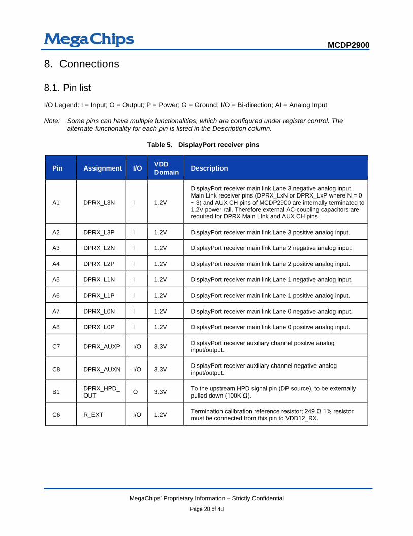
8. Connections
8.1. Pin list
I/O Legend: I = Input; O = Output; P = Power; G = Ground; I/O = Bi-direction; AI = Analog Input
Note: Some pins can have multiple functionalities, which are configured under register control. The alternate functionality for each pin is listed in the Description column.
Table 5. DisplayPort receiver pins
Pin Assignment I/O VDD Domain Description
A1 DPRX_L3N I 1.2V
DisplayPort receiver main link Lane 3 negative analog input. Main Link receiver pins (DPRX_LxN or DPRX_LxP where N = 0 ~ 3) and AUX CH pins of MCDP2900 are internally terminated to 1.2V power rail. Therefore external AC-coupling capacitors are required for DPRX Main LInk and AUX CH pins.
A2 DPRX_L3P I 1.2V DisplayPort receiver main link Lane 3 positive analog input.
A3 DPRX_L2N I 1.2V DisplayPort receiver main link Lane 2 negative analog input.
A4 DPRX_L2P I 1.2V DisplayPort receiver main link Lane 2 positive analog input.
A5 DPRX_L1N I 1.2V DisplayPort receiver main link Lane 1 negative analog input.
A6 DPRX_L1P I 1.2V DisplayPort receiver main link Lane 1 positive analog input.
A7 DPRX_L0N I 1.2V DisplayPort receiver main link Lane 0 negative analog input.
A8 DPRX_L0P I 1.2V DisplayPort receiver main link Lane 0 positive analog input.
C7 DPRX_AUXP I/O 3.3V DisplayPort receiver auxiliary channel positive analog input/output.
C8 DPRX_AUXN I/O 3.3V DisplayPort receiver auxiliary channel negative analog input/output.
B1 DPRX_HPD_OUT O 3.3V To the upstream HPD signal pin (DP source), to be externally
pulled down (100K Ω).
C6 R_EXT I/O 1.2V Termination calibration reference resistor; 249 Ω 1% resistor must be connected from this pin to VDD12_RX.

MCDP2900
MegaChips’ Proprietary Information – Strictly Confidential
Page 29 of 48
Table 6. HDMI output pins
Pin Assignment I/O VDD Domain Description
H1 HDMITX_CLKN O 3.3V HDMI transmitter CLOCK_N to TX connector.
H2 HDMITX_CLKP O 3.3V HDMI transmitter CLOCK_P to TX connector.
H3 HDMITX_CH0N O 3.3V HDMI transmitter DATA0_N to TX connector.
H4 HDMITX_CH0P O 3.3V HDMI transmitter DATA0_P to TX connector.
H5 HDMITX_CH1N O 3.3V HDMI transmitter DATA1_N to TX connector.
H6 HDMITX_CH1P O 3.3V HDMI transmitter DATA1_P to TX connector.
H7 HDMITX_CH2N O 3.3V HDMI transmitter DATA2_N to TX connector.
H8 HDMITX_CH2P O 3.3V HDMI transmitter DATA2_P to TX connector.
E1 HDMI_DDC_SCL O 3.3V, 5V TOL
HDMI TX DDC I2C master SCL. 3.3 V logic level, 5 V tolerant. Open drain, to be externally pulled up to DDC5V via a 1.5K ~ 2.2K Ω resistor.
F1 HDMI_DDC_SDA I/O 3.3V, 5V TOL
HDMI TX DDC I2C master SDA. 3.3 V logic level, 5 V tolerant. Open drain, to be externally pulled up to DDC5V via a 1.5K ~ 2.2K Ω resistor.
F2 HDMITX_CEC I/O 3.3V, 5V TOL
CEC input. 3.3 V open drain IO. Connect to HDMI CEC pin, to be externally pulled up to 3.3 V via 27K Ω resistor as per HDMI1.4b specification. Use weak external pull up or pull down (recommended 100K Ω) when CEC is not used.
G1 HDMITX_HDP_IN I 3.3V, 5V TOL
3.3 V logic level, 5 V tolerant input from HDMI connector. To be externally pulled down via 20K Ω resistor.
Note: HDMI TX output is terminated at the receiver through a 50 ohm resistor.

MCDP2900
MegaChips’ Proprietary Information – Strictly Confidential
Page 30 of 48
Table 7. System interface pins
Pin Assignment I/O VDD Domain
Reset State Description
B8 EXT_RESETN I 3.3 V Input Power-ON chip reset (active low) input signal, to be pulled up to 3.3V power rail via 2.2K Ω +/-10% resistor as shown in Figure 8.
E8 XTAL I/O 1.2V NA Connect to 27MHz crystal with 22pF to VDD12_OSC as shown in figure 5.
F8 TCLK I/O 1.2V NA Connect to 27 MHz crystal with 22pF to VDD12_OSC as shown in Figure 5.
F7 C_EXT O 3.3V NA Capacitor for filtering internal 2.5V LDOR. Connect to GND through 2.2uF capacitor.
G8 VDD12ON O 3.3 V Logic 1, output
1.2V power control signal. Reset State definition assumes 3.3V rail is ramped up to full voltage. Can be left NC.
E6 I2C_SDA IO 3.3 V Input, Internal PU
Host I2C interface data line up to 400kbps. Programmable Slew Rate and Drive Strength when this is being used as a GPIO.
F6 I2C_SCL I 3.3 V Input, internal PU
Host I2C interface clock line up to 400 kbps. Programmable Slew Rate and Drive Strength when this is being used as a GPIO.
C3 GPIO1_33 IO 3.3 V Input, Internal PD
3.3V General purpose input/output with programmable slew rate and drive control. Internal PD 50K Ohm.
F3 GPIO2_33 I/O 3.3V Input, internal PD
3.3V General purpose input/output with programmable slew rate and drive control. Internal PD 50K Ohm.
C1 SPI_CSN O 3.3 V Input, Internal PU
Serial peripheral interface chip select. Programmable Slew Rate and Drive Strength.
C2 SPI_DI I 3.3 V Input, Internal PD Serial peripheral interface data input.
D1 SPI_DO O 3.3 V Input, Internal PD
Serial peripheral interface data output. Programmable Slew Rate and Drive Strength.
D2 SPI_CLK O 3.3 V Input, Internal PD
Serial peripheral interface clock. Programmable Slew Rate and Drive Strength.
E2 SPI_WPN O 3.3 V Input, Internal PU
Serial peripheral interface write protect. Programmable Slew Rate and Drive Strength.
D7 UART_TX O 3.3 V Input, Internal PU
Universal asynchronous serial Tx output. Programmable Slew Rate and Drive Strength.

MCDP2900
MegaChips’ Proprietary Information – Strictly Confidential
Page 31 of 48
Pin Assignment I/O VDD Domain
Reset State Description
E7 UART_RX I 3.3 V Input, Internal PU
Universal asynchronous serial Rx input. Internal PU can be changed to Internal PD by register program.
Table 8. Power and ground pins
Pin Assignment Voltage Level Description
B2, C4 VDD33_RX 3.3 V DisplayPort RX analog power
B4, B5 VDD12_RX 1.2 V DisplayPort RX analog power
C5 VDD33_AUX 3.3 V DisplayPort AUX power
B7 VDD12_PLL 1.2 V PLL analog power
F4 VDD12_OSC 1.2 V Oscillator circuit power
G2, G4 VDD33_TX 3.3 V HDMI TX analog power
G5, G7 VDD12_TX 1.2 V HDMI TX analog power
D6, F5 VDD12_DIG 1.2 V Core and 1.2V IO power
D3, E3 VDD33_IO 3.3 V 3.3V IO power
B3, B6, D4, D5, E4, E5, G3, G6, D8 GND GND Power return for all supplies

MCDP2900
MegaChips’ Proprietary Information – Strictly Confidential
Page 32 of 48
8.2. Bootstrap configuration
DC levels on the bootstrap pins shown below are latched during the de-asserting edge of power-on reset
(EXT_RESETN goes HIGH). The levels specified below must be adhered to for the normal function of the
device.
Table 9. Bootstrap configuration
Bootstrap signal name
Internal PU/PD Assignment Function
Bootstrap ‘0’ PULLUP UART_TX (D7) RESERVED. Leave as NC.
Bootstrap ‘1’ PULLUP SPI_WPN (E2) RESERVED. Leave as NC.
Bootstrap ‘2’ PULLDN SPI_CLK (D2) RESERVED. Leave as NC.
Bootstrap ‘3’ PULLDN SPI_DO (D1) RESERVED. Leave as NC.
Bootstrap ‘4’ PULLUP SPI_CSN (C1) RESERVED. Leave as NC.
Bootstrap ‘5’ PULLDN GPIO1_33 (C3) Can be used for customized application configuration.
Bootstrap ‘6’ PULLDN GPIO2_33 (F3) Can be used for customized application configuration.
Note: When the pin corresponding to a specific bootstrap is left NC, the pin takes the value of the assigned by the internal PULLUP (Level 1) or PULLDN (Level 0). The internal resistor used is around 50 k Ω. To select a non-default value on a bootstrap, an external PULLUP or PULLDN resistor tied to the opposite direction that overcomes the internal PULLUP or PULLDN needs to be used.
8.3. EXT_RESETN connection
The EXT_RESETN pin must be pulled up to 3.3 V via a 2.2 Kohm +/- 10% resistor as shown below. The chip
also supports an active low, external reset pulse to EXT_RESETN allowing a system host controller to reset
the system. The recommended way to drive EXT_RESETN is through an open-drain output. Alternately, if an
open-drain output is not available, the series resistor shown in the figure below is required.

MCDP2900
MegaChips’ Proprietary Information – Strictly Confidential
Page 33 of 48
Figure 8. EXT_RESETN Connection to MCDP2900
System Host
External Reset Control (optional)
3.3VMCDP2900
RESETNExternal Reset Switch (for debug)External 1.5K to 3Kohm
+/-1% series res is tor
2.2Kohm
Capacitor Value should not exceed
50pF

MCDP2900
MegaChips’ Proprietary Information – Strictly Confidential
Page 34 of 48
9. Package Package type: LFBGA (7x7x1.4 mm, 64, F8x8, Pitch 0.8, Ball 0.4)
9.1. Package drawing
Figure 9. MCDP2900 package drawing

MCDP2900
MegaChips’ Proprietary Information – Strictly Confidential
Page 35 of 48
9.2. LFBGA 7 x 7 dimensions
Table 10. MCDP2900 package dimensions

MCDP2900
MegaChips’ Proprietary Information – Strictly Confidential
Page 36 of 48
9.4. Marking field template and descriptors
The MCDP2900 marking template is shown below: Figure 10. Marking template
Field descriptors are shown below.
Table 11. Field descriptors
Field Description Marking
A Standard MegaChips logo MegaChips B Product code MCDP2900A2 C 2-character diffusion plant code VQ D 3-digit wafer start date “YWW” E 3-character FE sequence code “ABC” F 2-character assembly plant code 99 G 3-character BE sequence code “XYZ” H Optional marking FX or <blank> I 3-character country of origin code MYS J 2-character test plant code 8U K 1-digit assembly year “Y” L 2-digit assembly week “WW” M Ball A1 identifier a DOT
9.5. Classification reflow profile
Please refer to the DisplayPort Application Note: Classification reflow profile for SMD devices (C0353-APN-06) for reflow diagram and details.

MCDP2900
MegaChips’ Proprietary Information – Strictly Confidential
Page 37 of 48
10. Electrical specifications
10.1. Absolute maximum ratings
Applied conditions greater than those listed under “Absolute maximum ratings”, may cause permanent
damage to the device. The device should never exceed absolute maximum conditions since it may affect
device reliability.
Table 12. Absolute maximum ratings
Parameter Symbol Min Typ Max Units
3.3 V supply voltages (1,2) VVDD_3.3 -0.3 3.3 3.96 V
1.2 V supply voltages (1.2) VVDD_1.2 -0.3 1.2 1.44 V
Input voltage tolerance for 3.3 V, 5 V tolerant I/O pins VIN5tol -0.3 5.5 V
Input voltage tolerance for 3.3 V I/O pins VIN3V3 -0.3 3.75 V
ESD – Human Body Model (HBM)[ JESD22-A114 spec] For all pins
VESD - - +/- 2.0 kV
ESD – Human Body Model (HBM) [IEC61000-4 spec] For DP and HDMI connector-facing pins
VESD - - +/- 6.5 kV
ESD – Charged Device Model (CDM) [JESD22-C101 spec] VESD - - +/- 500 V
Latch-up [JESD78 spec] ILA - - +/- 100 mA
Ambient operating temperature TA 0 - 70 °C
Storage temperature TSTG -40 - 150 °C
Operating junction temperature TJ 0 75 125 °C
Thermal resistance (Junction to Ambient)(3) θJA - - 37.6 °C/W
Thermal resistance (Junction to Case)(3) θJC - - 18.8 °C/W
Peak IR reflow soldering temperature TSOL - - 260 °C
Note 1: All voltages are measured with respect to GND.
Note 2: Absolute maximum voltage ranges are for transient voltage excursions.
Note 3: These are simulated results under the following conditions – Four layer JEDEC PCB, no heat
spreader, Air flow = 0 m/s.
MCDP2900
MegaChips’ Proprietary Information – Strictly Confidential
Page 38 of 48
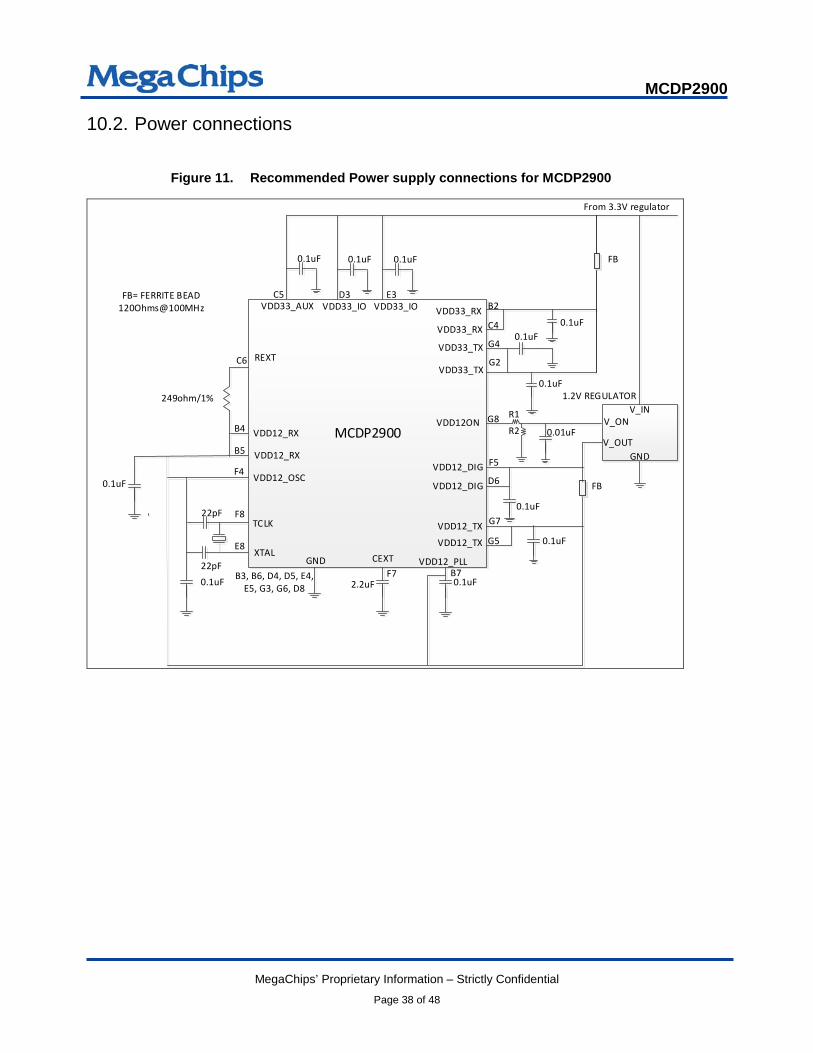
10.2. Power connections
Figure 11. Recommended Power supply connections for MCDP2900
MCDP2900
REXT
VDD33_RX
249ohm/1%
0.1uF
0.1uF
VDD12_TX
VDD12_RX
VDD33_TX
VDD12_OSC
VDD12_PLL
TCLK
XTAL
0.1uF22pF
22pF
GND
VDD33_IO
VDD12_DIG
0.1uF
0.1uF
From 3.3V regulator
0.1uF
CEXT
2.2uF
0.1uF
VDD12ON0.01uF
R1
R2V_ON
V_OUTGND
V_IN1.2V REGULATOR
B2D3 E3
VDD33_IO
G2
G4VDD33_TX
0.1uF
VDD33_RX C4
C6
VDD12_RXB4
B5
F4
F8
E8
B3, B6, D4, D5, E4, E5, G3, G6, D8
F7
VDD12_DIG D6
F5
G7VDD12_TXG5
0.1uF
G8
VDD33_AUXC5FB= FERRITE BEAD
120Ohms@100MHz
FB
FB
0.1uF
B7
0.1uF

MCDP2900
MegaChips’ Proprietary Information – Strictly Confidential
Page 39 of 48
10.3. DC characteristics
Table 13. DC characteristics
Parameter Symbol Min Typ Max Units
3.3 V supply voltages (analog and digital) VVDD_1.8 3.14 3.3 3.47 V
1.2 V supply voltages (analog and digital) VVDD_1.2 1.14 1.2 1.26 V
Power
Protocol converter Mode Measurement condition: Nominal corner, 25°C, Nominal power supply 4k x 2k / 60 Hz 4L HBR2-to-HDMI test pattern: ON-OFF
482 570 mW
4k x 2k / 30 Hz 4L HBR2-to-HDMI test pattern: ON-OFF
413 480 mW
1920 x 1080 / 60 Hz 4L HBR2-to-HDMI test pattern: ON-OFF 380 440 mW
Sleep 11 mW
Connected Standby 4 mW
Supply Current
Measurement conditions: Nominal corner, 25°C, Nominal power supply 4k x 2k @60 MHz 4L HBR to HDMI2.0a VDD (analog and digital) 3.3V VDD (analog and digital) 1.2V
25 332
27 390
mA
Note: Ripple amplitude for power supplies should be 30 mV or lower with max ripple freq up to 30 MHz.

MCDP2900
MegaChips’ Proprietary Information – Strictly Confidential
Page 40 of 48
Table 14. IO DC characteristics
Parameter Symbol Min Typ Max Unit
Inputs 3.3 V IO signals, 5 V tolerant open drain type
High voltage VIH 2.0 5.5 V
Low voltage VIL -0.3 0.8 V
Input Hysteresis voltage VHYST 300 mV
High current (VIN = 3.3 V) IIH +/- 10 µA
Low current (VIN = 0.8 V) IIL +/- 10 µA
Input capacitance CIN 5 pF
Outputs 3.3 V IO signals, 5 V tolerant open drain type
Low Current (VOL = 0.2 V) IOL 4 mA
Tri-state leakage current IOZ 10 µA
VDD12ON Output
Output Low Voltage (IOL=0.25mA) VOL 0.4 V
Output High Voltage(IOH=0.25mA) VOH 2.9 V
Low Level output Current IOL 0.25
High Level Output Current IOH 0.25
Inputs 3.3 V IO signals, 3.3 V tolerant, TRISTATE
High voltage VIH 2.0 V
Low voltage VIL 0.8 V
Input Hysteresis voltage VHYST 300 mV
High current (VIN = 3.3 V) IIH ±10 µA
Low current (VIN = 0.8 V) IIL ±10 µA
Input capacitance CIN 1.0 pF
Outputs 3.3 V IO signals, 3.3 V tolerant, TRISTATE
Output Impedance, VOL=0.3V Rout 50 Ω
Tri-state leakage current IOZ ±10 mA

MCDP2900
MegaChips’ Proprietary Information – Strictly Confidential
Page 41 of 48
10.4. AC characteristics
Table 15. Maximum speed of operation
Clock domain Max speed of operation
Reference Input Clock (TCLK) 27 MHz
Reference Internal Clock (RCLK) 324 MHz
On-Chip Microcontroller Clock (OCLK) 150 MHz
2-Wire Serial Slave (SLAVE_SCL) 400 kHz
DDC Master (MSTRx_SCL) 400 kHz
SPI Clock 50 MHz
10.4.1. DisplayPort receiver
Table 15. DisplayPort receiver characteristics
Parameter Symbol Min Typ Max Units Comments
Receiver operating range
Differential Input Voltage Range VRX_DIF_PP_RANGE 0.04~1 V
RX Termination Control Range RRX_TERM_RANGE 80 ~120 ohm
DisplayPort receiver system parameters
HBR2 unit interval (5.4Gbps) UIHBR2 185 ps
HBR unit interval (2.7Gbps) UIHBR 370 ps
RBR unit interval (1.62Gbps) UIRBR 617 ps
Link clock down spreading 0 0.5 % Modulation frequency range 0f 30 kHz to 33 kHz
DisplayPort receiver TP3 parameters
Receiver Eye TP3 RBR TRBR_EYE_TP3 0.25 UI @ 40mV V_diff_pp
Receiver Eye TP3_EQ HBR THBR_EYE_TP3EQ 0.4 UI @ 135mV V_diff_pp
Receiver Eye TP3_EQ HBR2 THBR2_EYE_TP3EQ 0.3 UI @ 70mV V_diff_pp
Lane intra-pair skew tolerance
TSKEW_INTRA_RBR 260 ps
Skew contribution from the cable in addition to the stressed EYE at TP3. TSKEW_INTRA_HBR 60 ps
TSKEW_INTRA_HBR2 50 ps

MCDP2900
MegaChips’ Proprietary Information – Strictly Confidential
Page 42 of 48
Parameter Symbol Min Typ Max Units Comments
Target bit error rate 10-9
Non-ISI at 1.62 Gbps TRX_Non-ISI_RBR 0.180 UI 1.62Gbps signal @ TP3
TJ at 1.62 Gbps TRX_TJ_RBR 0.750 UI 1.62Gbps signal @ TP3
Non-ISI at 2.7 Gbps TRX_Non-ISI_HBR 0.330 UI 2.7Gbps signal @ TP3_EQ
TJ at 2.7 Gbps TRX_TJ_HBR 0.491 UI 2.7 Gbps signal @ TP3_EQ
DJ at 5.4 Gbps TRX_DJ_HBR2 0.49 UI 5.4 Gbps signal @ TP3_EQ
TJ at 5.4 Gbps TRX_TJ_HBR2 0.62 UI 5.4 Gbps signal @ TP3_EQ
AUX parameters
Differential Input Voltage Range VAUX_RX_DIF_RANGE 0.14~1 V
RX Termination Control Range RAUX_TERM_RANGE 40~60 ohms
AUX TX peak-peak Range VAUX_TX_DIF_PP 0~1 V 7.8125mV/step in 128 steps
10.4.2. HDMI transmitter I/O specifications
Table 16. HDMI transmitter DC specifications
Parameters Symbol Min Typ Max Unit Comments
Differential output: single ended swing amplitude
VTX_PP 0.4 0.5 0.6 V
Differential output: Differential swing amplitude
VTX_DIF_PP 0.8 1 1.2 V
Differential high level output VTX_DIF_HIGH 3.12 3.3 3.49 V
Differential low level output VTX_DIF_LOW 3.12 3.49 V

MCDP2900
MegaChips’ Proprietary Information – Strictly Confidential
Page 43 of 48
Table 17. HDMI transmitter AC characteristics
Parameters Symbol Min Typ Max Unit Comments TMDS Character Clock
fTX_CHR_CLK 25 600 MHz Programmable Differential Output Voltage
VTX_DIF_PP 0 1200 mV In 128 steps TX Edge Rate
tTX_ER 75 145 pS 1V VTX_DIF_PP and Premphasis at 0dB in 8 steps
TX Pre-Emphasis Level APREMPH 0 6 dB 1V VTX_DIF_PP in 16 steps
TX Termination Control Range RTX_TERM_RANGE 100 600 ohms Programmable
Termination TX Jitter <1.65Gbps for Pattern
D10.2 TTX_J_D102_LF 60 pS
TX Jitter <1.65Gbps for PatternPRBS7 TTX_J_PRBS7_LF 70 pS
TX Jitter >1.65Gbps, < 3.4Gbps for PatternD10.2 TTX_J_D102_MF 35 pS
TX Jitter >1.65Gbps, < 3.4Gbps for PatternPRBS7 TTX_J_PRBS7_MF 45 pS
TX Jitter >3.4Gbps for PatternD10.2 TTX_J_D102_HF 30 pS
TX Jitter >3.4Gbps for PatternPRBS7 TTX_J_PRBS7_HF 35 pS
10.4.3. I2C interface timing
Table 18. I2C interface timing
Symbol Parameter Conditions Min Typ Max Unit
fSCL SCL clock rate Fast mode 0 - 400 kHz
tHD-STA Hold time START After this period, the 1st clock starts 1.2 - - µs
tLOW Low period of clock SCL 1.3 - - µs
tHIGH High period of clock SCL 1.2 - - µs
Tsu;STA Set up time for a repeated START 1.2 - - µs
tHD;DAT Data hold time For master 0.7 - 0.9(1) µs
tSU;DAT Data setup time 380 - - ns
TBUF Bus free time between STOP 1.3 - - µs
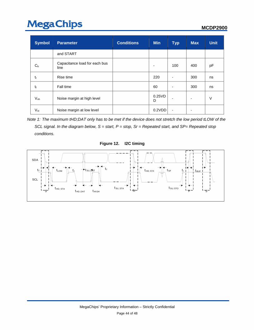
MCDP2900
MegaChips’ Proprietary Information – Strictly Confidential
Page 44 of 48
Symbol Parameter Conditions Min Typ Max Unit
and START
Cb Capacitance load for each bus line - 100 400 pF
tr Rise time 220 - 300 ns
tf Fall time 60 - 300 ns
Vnh Noise margin at high level 0.25VDD - - V
Vnl Noise margin at low level 0.2VDD - -
Note 1: The maximum tHD;DAT only has to be met if the device does not stretch the low period tLOW of the
SCL signal. In the diagram below, S = start, P = stop, Sr = Repeated start, and SP= Repeated stop
conditions.
Figure 12. I2C timing
SDA
SCL
t f
S
t LOW t r t f t SU ; DAT t HD ; STA t SP t r t BUF
S P t HD ; STA t HD ; DAT t HIGH
t SU ; STA Sr t SU ; STO

MCDP2900
MegaChips’ Proprietary Information – Strictly Confidential
Page 45 of 48
10.4.4. SPI interface timing
The table below specifies the typical SPI_CLK output frequency and the minimum requirements of the
interface between the SPI NOR Flash device and the MCDP2900 SPI interface.
Table 19. SPI interface timing
Symbol Parameter Min Typ Max Units
FCLK SPI_CLK output clock frequency 50 MHz
TSCKH Serial clock high time 20 ns
TSCKL Serial clock low time 20 ns
TR_SPI_CLK SPI_CLK rise time @10mA drive 10pF load 2.8 ns
TF_SPI_CLK SPI_CLK fall time @10mA drive 10pF load 3.2 ns
TCSN_SU CSN output setup time requirement 7 ns
TCSN_HLD CSN output hold time requirement 7 ns
T_DO_PD Data Output propagation delay 6 ns
TDI_SU Data Input setup time 3 ns
TDI_HLD Data Input hold time 5 ns

MCDP2900
MegaChips’ Proprietary Information – Strictly Confidential
Page 46 of 48
11. Ordering information Table 20. Order codes
Part number Description
MCDP2900A2 64 LFBGA (7x7x1.4 mm) in Tray
MCDP2900A2T 64 LFBGA (7x7x1.4 mm) in Tape & Reel
MCDP2900A2 FX 64 LFBGA (7x7x1.4 mm) in Tray

MCDP2900
MegaChips’ Proprietary Information – Strictly Confidential
Page 47 of 48
12. Revision history
Table 21. Document revision history Date Revision Changes
26-MAY-2015 A Initial version.
20-Nov-2015 B Updated clock generation section and electrical specification section.
14-Apr-2016 C Updated with changes throughout the datasheet. Added sleep and standby power numbers in to DC Characteristics.
29-Apr-2016 D Updated Figure 11: Recommended Power supply connections for MCDP2900, Table 15: DP Receiver jitter parameters, and Table 19: SPI timing parameters.

MCDP2900
MegaChips’ Proprietary Information – Strictly Confidential
Page 48 of 48
Notice
Semiconductor products may possibly experience breakdown or malfunction. Adequate care should be taken with respect to the safety design of equipment in order to prevent the occurrence of human injury, fire or social loss in the event of breakdown or malfunction of semiconductor products
The overview of operations and illustration of applications described in this document indicate the conceptual method of use of the semiconductor product and do not guarantee operability in equipment in which the product is actually used.
The names of companies and trademarks stated in this document are registered trademarks of the relevant companies.
MegaChips Co. provides no guarantees nor grants any implementation rights with respect to industrial property rights, intellectual property rights and other such rights belonging to third parties or/and MegaChips Co. in the use of products and of technical information including information on the overview of operations and the circuit diagrams that are described in this document.
The product described in this document may possibly be considered goods or technology regulated by the Foreign Currency and Foreign Trade Control Law. In the event such law applies, export license will be required under said law when exporting the product. This regulation shall be valid in Japan domestic.
In the event the intention is to use the product described in this document in applications that require an extremely high standard of reliability such as nuclear systems, aerospace equipment or medical equipment for life support, please contact the sales department of MegaChips Co. in advance.
All information contained in this document is subject to change without notice.
Copyright © 2015 MegaChips Corporation All rights reserved
Contact MegaChips Corporation Head Quarters 1-1-1 Miyahara, Yodogawa-ku Osaka 532-0003, Japan TEL: +81-6-6399-2884 MegaChips Corporation Tokyo Office 17-6 Ichiban-cho, Chiyoda-ku, Tokyo 102-0082, Japan TEL: +81-3-3512-5080 MegaChips Corporation Makuhari Office 1-3 Nakase Mihama-ku Chiba 261-8501, Japan TEL: +81-43-296-7414 MegaChips Corporation San Jose Office 2033 Gateway Place, Suite 400, San Jose, CA 95110 U.S.A. TEL: +1-408-570-0555 MegaChips Corporation India Branch 17th Floor, Concorde Block UB City, Vittal Mallya Road, Bangalore 560-001, India
MegaChips Corporation Taiwan Branch RM. B 2F, Worldwide House, No.129, Min Sheng E. Rd., Sec. 3, Taipei 105, Taiwan TEL: +886-2-2547-1297 MegaChips Corporation Tainan Office RM. 2, 8F, No.24, Da Qiao 2 Rd., Yong Kang Dist., Tainan 710, Taiwan TEL: +886-6-302-2898 MegaChips Corporation Zhunan Office No.118, Chung-Hua Rd., Chu-Nan, Miao-Li 350, Taiwan TEL: +886-37-666-156 MegaChips Corporation Shenzhen Office Room 6307, Office Tower, Shun Hing Square, 5002 Shen Nan Dong Road, Luohu District, Shenzhen 518000, P. R. China TEL: +86-755-3664-6990
TEL: +91-80-4041-3999