mcs-51 hardware interfacing - unimap portalportal.unimap.edu.my/portal/page/portal30/lecturer...
TRANSCRIPT
MCS-51 Hardware Interfacing
1
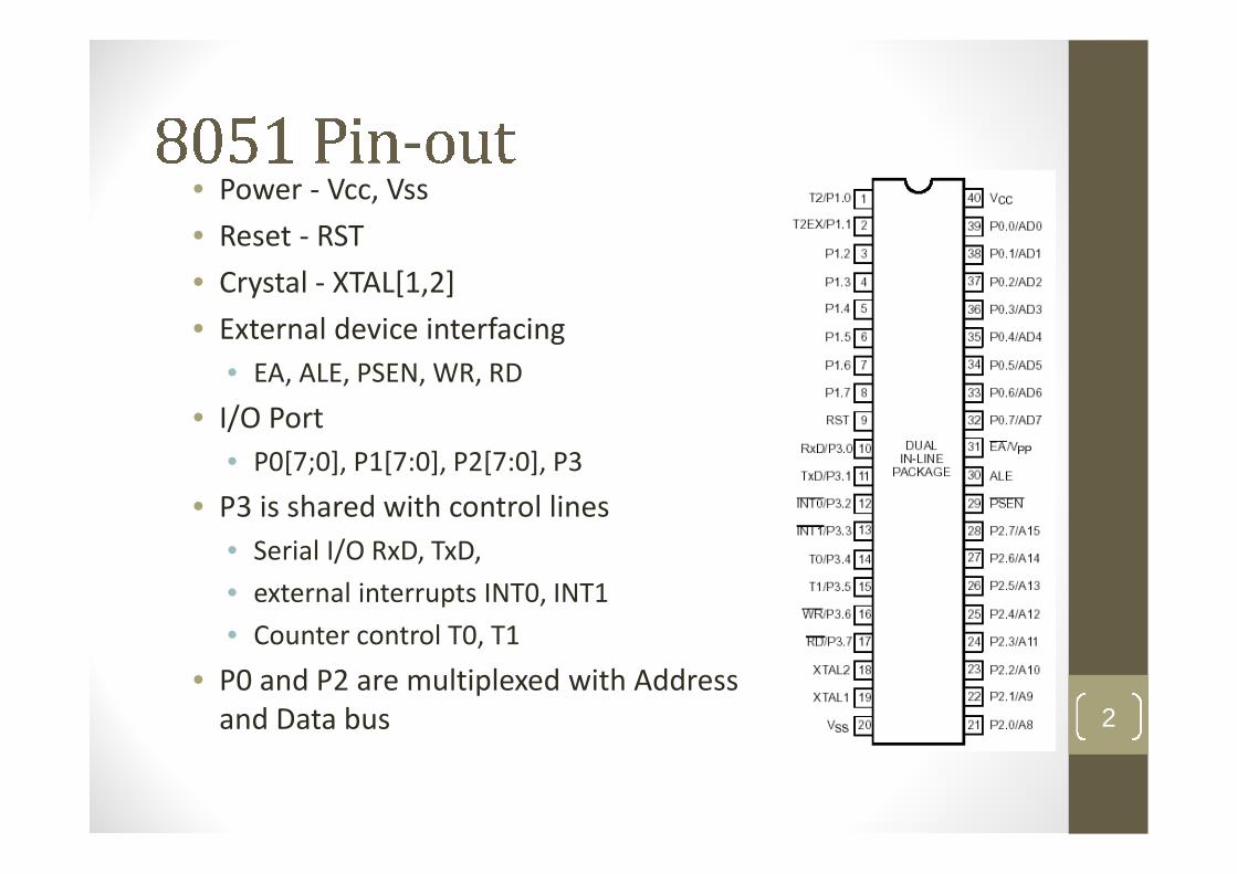
• Power - Vcc, Vss
• Reset - RST
• Crystal - XTAL[1,2]
• External device interfacing
• EA, ALE, PSEN, WR, RD
• I/O Port
• P0[7;0], P1[7:0], P2[7:0], P3
• P3 is shared with control lines
• Serial I/O RxD, TxD,
• external interrupts INT0, INT1
• Counter control T0, T1
• P0 and P2 are multiplexed with Addressand Data bus 2
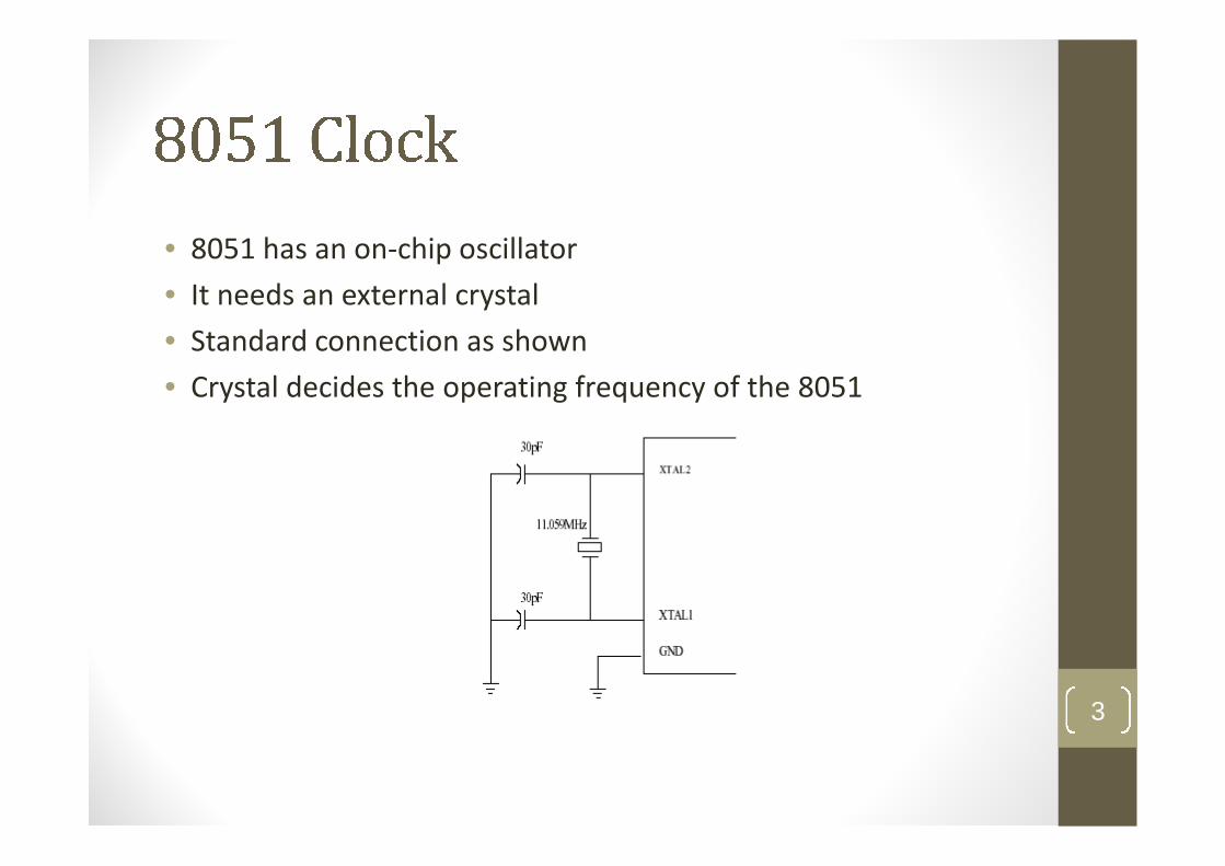
• 8051 has an on-chip oscillator
• It needs an external crystal
• Standard connection as shown
• Crystal decides the operating frequency of the 8051
3
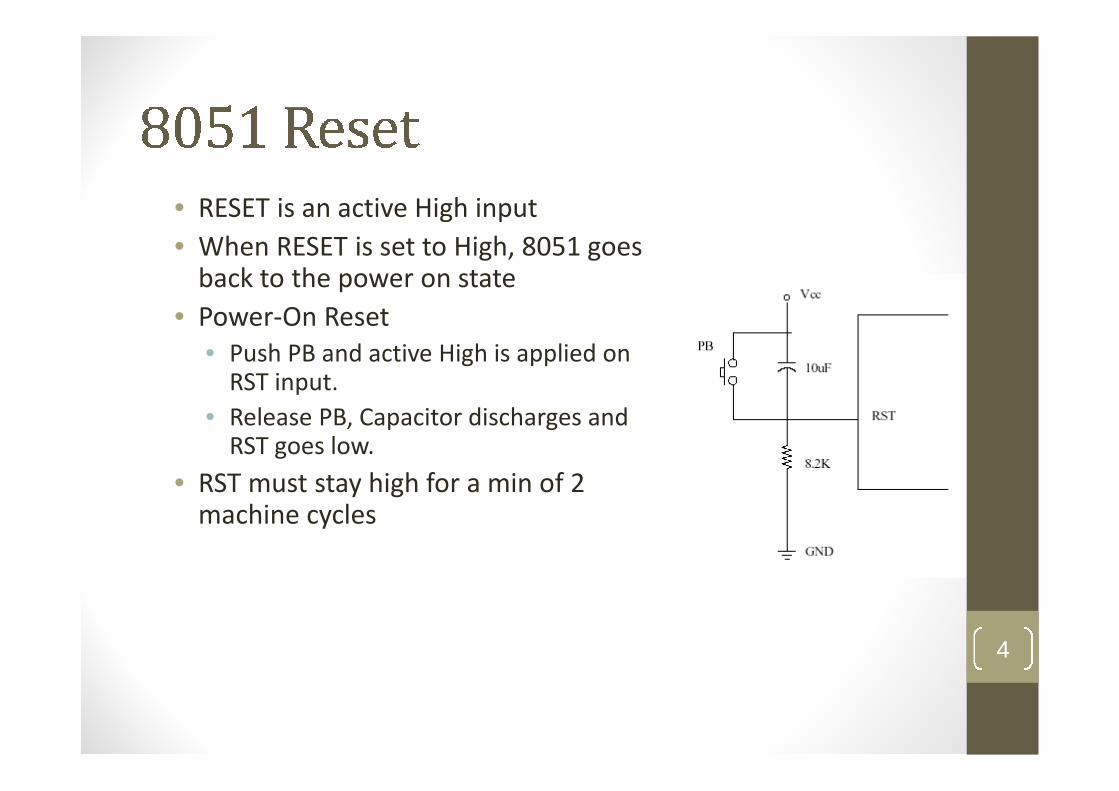
• RESET is an active High input
• When RESET is set to High, 8051 goesback to the power on state
• Power-On Reset• Push PB and active High is applied on
RST input.
• Release PB, Capacitor discharges andRST goes low.
• RST must stay high for a min of 2machine cycles
4
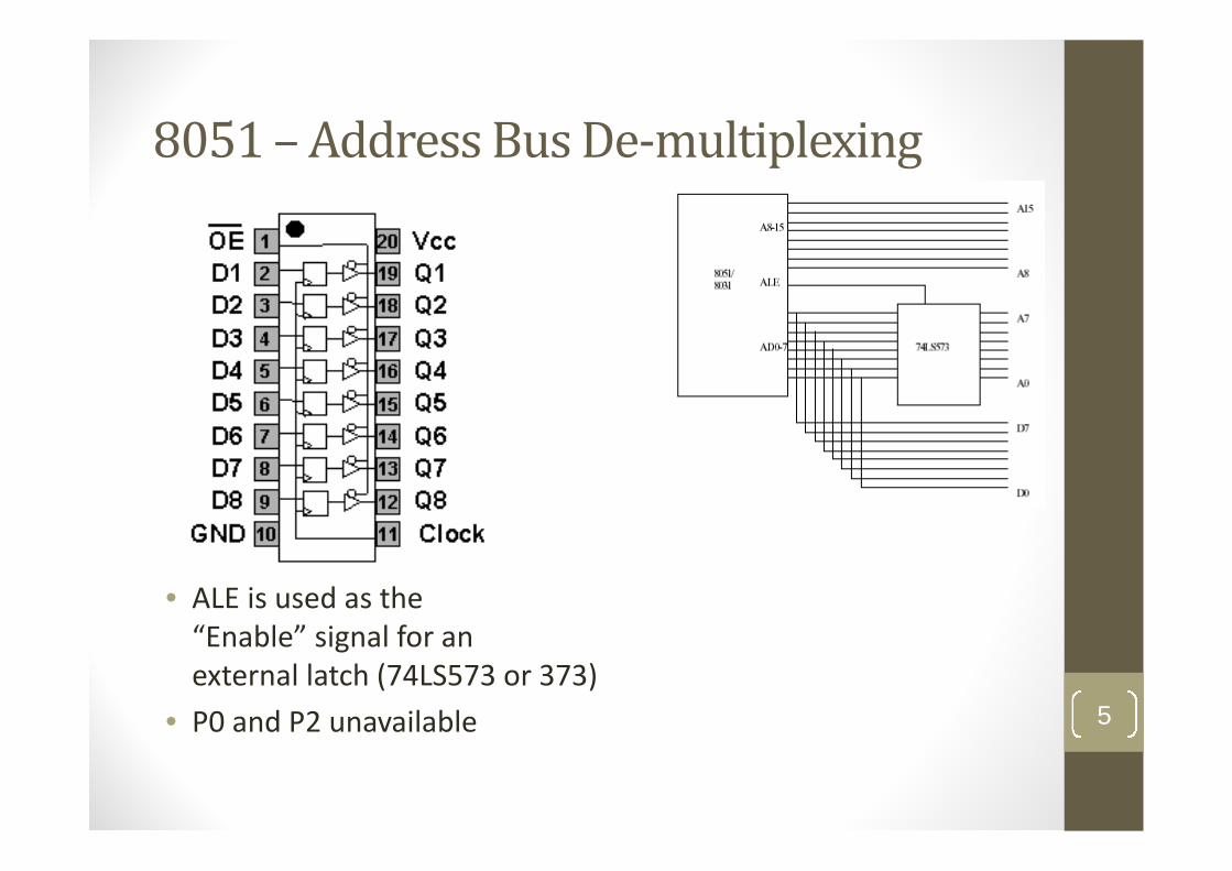
8051 – Address Bus De-multiplexing
•ALE – Address LatchEnable
•8051 drives it highwhen address is
available on AD[7,0]
• ALE is used as the“Enable” signal for anexternal latch (74LS573 or 373)
• P0 and P2 unavailable 5
8051 External Code Memory Access
• 8051 devices can have either on-chip or external code ROM
• Input pin EA decides which is used and PSEN is used to enableit.
• EA is an active low input to 8051• EA connected to GND (Low) means 8051 uses external memory
for code
• EA connected to Vcc (High) means 8051 uses on-chip ROM forcode memory
• PSEN – Program Store Enable, active low• Connect this to the OE (output enable) of external ROM device
6
Microprocessor Interfacing - Basics
• Any CPU (8051) has
• Address bus A[15:0]
• Data bus D[7:0]
• Control lines : ALE, PSEN, RD, WR
• A Single Processor mP based system has one CPU and manydevices interfaced to it
• Only one Address bus and one data bus in a Single Processorsystem
• ABUS and DBUS are common for all interfaced devices and theCPU
7
Microprocessor Interfacing (contd.)
• All Microprocessor compatible devices have enable lines (CE -Chip Enable or CS – Chip Select)
• A function of the address bus f(A[15:0]) is connected to the CE ofevery device interfaced
• This function is unique for every interfaced device
• The CPU accesses each interfaced device by way of this uniquefunction
• This function is commonly referred to as the address of thedevice
8
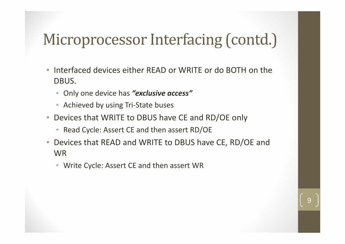
Microprocessor Interfacing (contd.)
• Interfaced devices either READ or WRITE or do BOTH on theDBUS.
• Only one device has “exclusive access”
• Achieved by using Tri-State buses
• Devices that WRITE to DBUS have CE and RD/OE only
• Read Cycle: Assert CE and then assert RD/OE
• Devices that READ and WRITE to DBUS have CE, RD/OE andWR
• Write Cycle: Assert CE and then assert WR
9
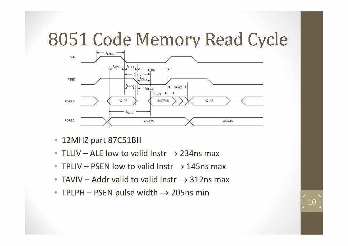
• 12MHZ part 87C51BH
• TLLIV – ALE low to valid Instr 234ns max
• TPLIV – PSEN low to valid Instr 145ns max
• TAVIV – Addr valid to valid Instr 312ns max
• TPLPH – PSEN pulse width 205ns min10
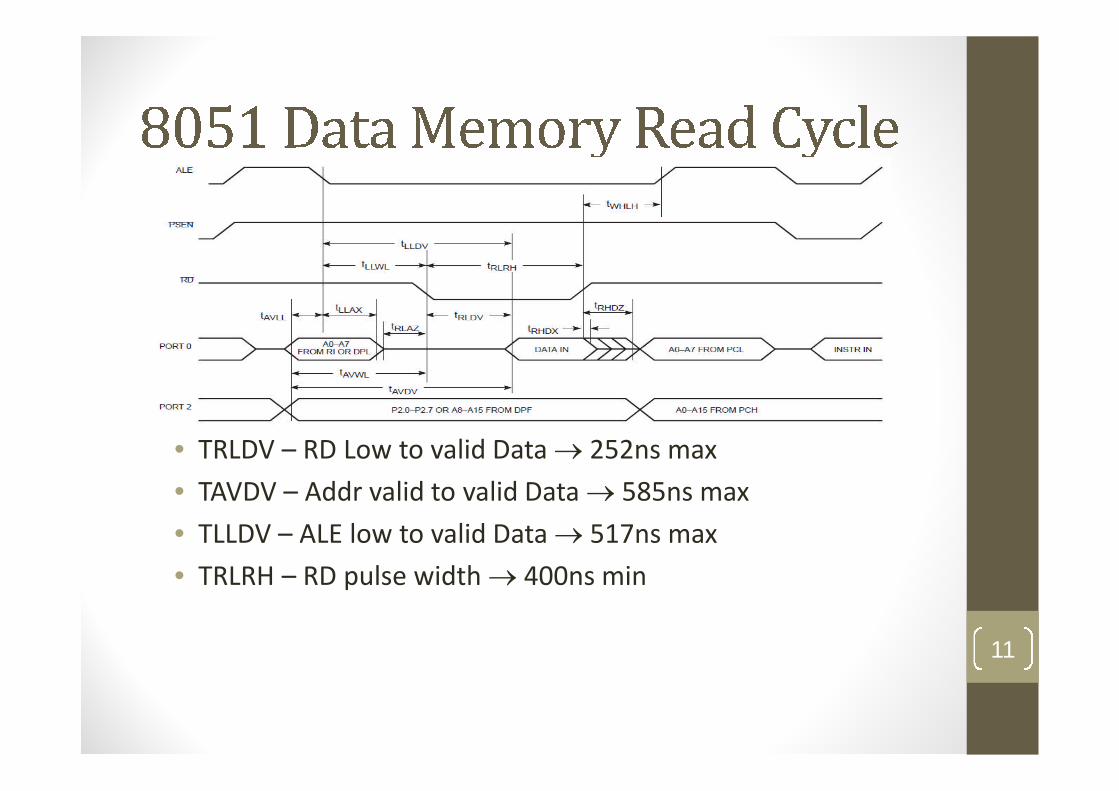
• TRLDV – RD Low to valid Data 252ns max
• TAVDV – Addr valid to valid Data 585ns max
• TLLDV – ALE low to valid Data 517ns max
• TRLRH – RD pulse width 400ns min
11
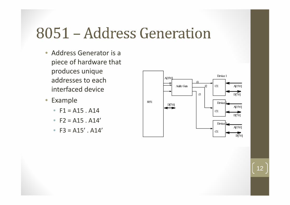
• Address Generator is apiece of hardware thatproduces uniqueaddresses to eachinterfaced device
• Example
• F1 = A15 . A14
• F2 = A15 . A14’
• F3 = A15’ . A14’
12
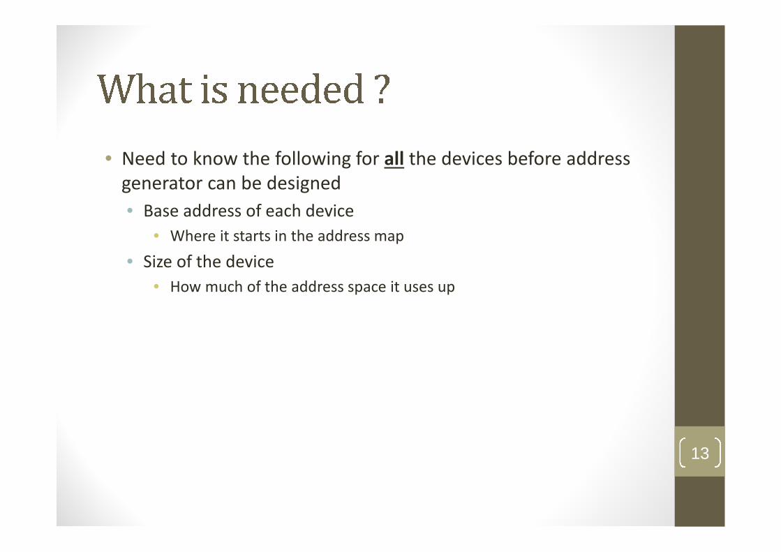
• Need to know the following for all the devices before addressgenerator can be designed
• Base address of each device
• Where it starts in the address map
• Size of the device
• How much of the address space it uses up
13
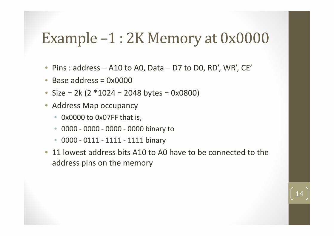
Example –1 : 2K Memory at 0x0000
• Pins : address – A10 to A0, Data – D7 to D0, RD’, WR’, CE’
• Base address = 0x0000
• Size = 2k (2 *1024 = 2048 bytes = 0x0800)
• Address Map occupancy
• 0x0000 to 0x07FF that is,
• 0000 - 0000 - 0000 - 0000 binary to
• 0000 - 0111 - 1111 - 1111 binary
• 11 lowest address bits A10 to A0 have to be connected to theaddress pins on the memory
14
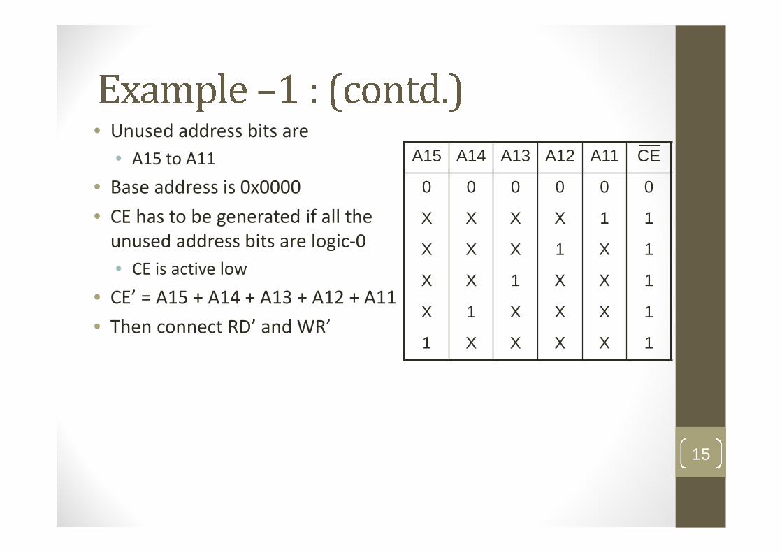
• Unused address bits are
• A15 to A11
• Base address is 0x0000
• CE has to be generated if all theunused address bits are logic-0
• CE is active low
• CE’ = A15 + A14 + A13 + A12 + A11
• Then connect RD’ and WR’
15
A15 A14 A13 A12 A11 CE
0 0 0 0 0 0
X X X X 1 1
X X X 1 X 1
X X 1 X X 1
X 1 X X X 1
1 X X X X 1
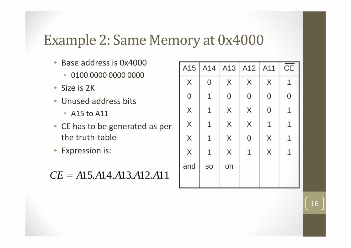
Example 2: Same Memory at 0x4000
• Base address is 0x4000
• 0100 0000 0000 0000
• Size is 2K
• Unused address bits
• A15 to A11
• CE has to be generated as perthe truth-table
• Expression is:
16
A15 A14 A13 A12 A11 CE
X 0 X X X 1
0 1 0 0 0 0
X 1 X X 0 1
X 1 X X 1 1
X 1 X 0 X 1
X 1 X 1 X 1
and so on
11.12.13.14.15 AAAAACE
Complete vs. Partial Address Decoding
• Complete address decoding:• Use all unused address bits to generate CE
• Partial addressing decoding• Use a sub-set of the unused address bits
• Used to reduce the address generator complexity
• Produces address mirrors (same device at multiple addresses)
• Example• 2K memory at 0x0000, we used A15 to A11
• Instead just connect A11 to CE
• Same 2K memory device will then be mirrored for all values ofA15 to A12
• 0x0000, 0x1000, 0x2000, 0x3000, …. , 0xF000
• Address generator became very simple, but we lost a lot ofaddress space
17
74138 Decoder for Address Generation
• 3 to 8 decoder, available in a single DIP package.
• Takes 3 address lines and generates complete addressingamong those
• Example• Connect A15, A14, A13 to the decoder inputs
• Decoder outputs give base addresses for• 0x0000, 0x2000, 0x4000, 0x6000,0x8000, 0xA000, 0xC000, 0xE000
• For more complicated address decoding:• Play tricks with 74138 enable connections.
• Use programmable devices like PALs, PLDs or FPGAs
18
• Could be RAM or ROM
• Address generation as per standard procedure
• Connect PSEN’ to the OE’ of the memory device
• RD’ and WR’ are ignored
• Connect Data bits D7-D0 of the memory and the 8051
19
• Address generation as per standard procedure
• Logically AND PSEN’ and RD’ and then connect to the OE’ ofthe memory
• Connect WR’ from the 8051 to WR of the memory
• Connect Data bits D7-D0 of the memory and the 8051
20
• Same procedure as for interfacing memory
• Only difference is that these devices have smaller sizes anduse smaller portions of the address space
• Example:
• 8 LEDS connected to an 8-bit latch. The latch is address mappedto 0xF000. Size is 1byte
• 8255 I/O device memory mapped at 0xD000. Size is 4 bytes
21
22
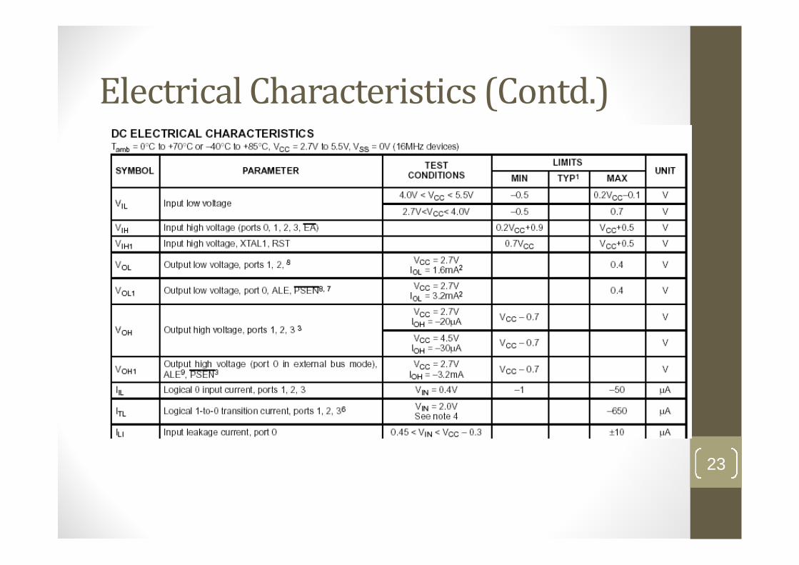
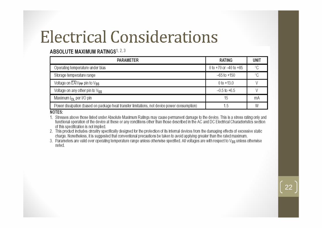
Electrical Characteristics (Contd.)
23
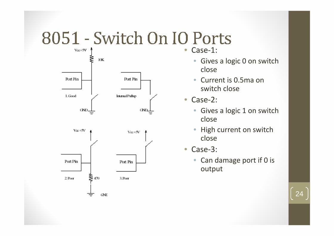
• Case-1:• Gives a logic 0 on switch
close
• Current is 0.5ma onswitch close
• Case-2:• Gives a logic 1 on switch
close
• High current on switchclose
• Case-3:• Can damage port if 0 is
output
24
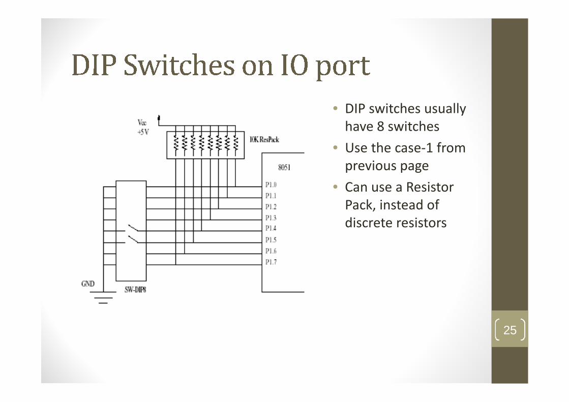
• DIP switches usuallyhave 8 switches
• Use the case-1 fromprevious page
• Can use a ResistorPack, instead ofdiscrete resistors
25
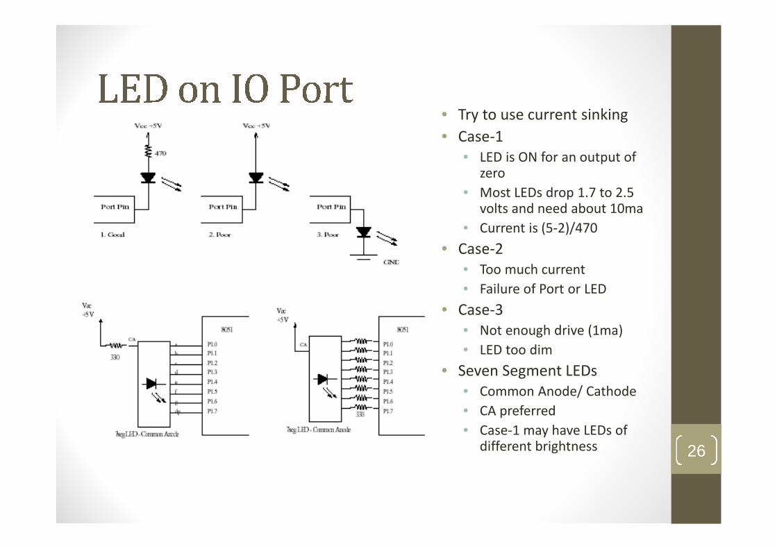
• Try to use current sinking
• Case-1• LED is ON for an output of
zero
• Most LEDs drop 1.7 to 2.5volts and need about 10ma
• Current is (5-2)/470
• Case-2• Too much current
• Failure of Port or LED
• Case-3• Not enough drive (1ma)
• LED too dim
• Seven Segment LEDs• Common Anode/ Cathode
• CA preferred
• Case-1 may have LEDs ofdifferent brightness 26
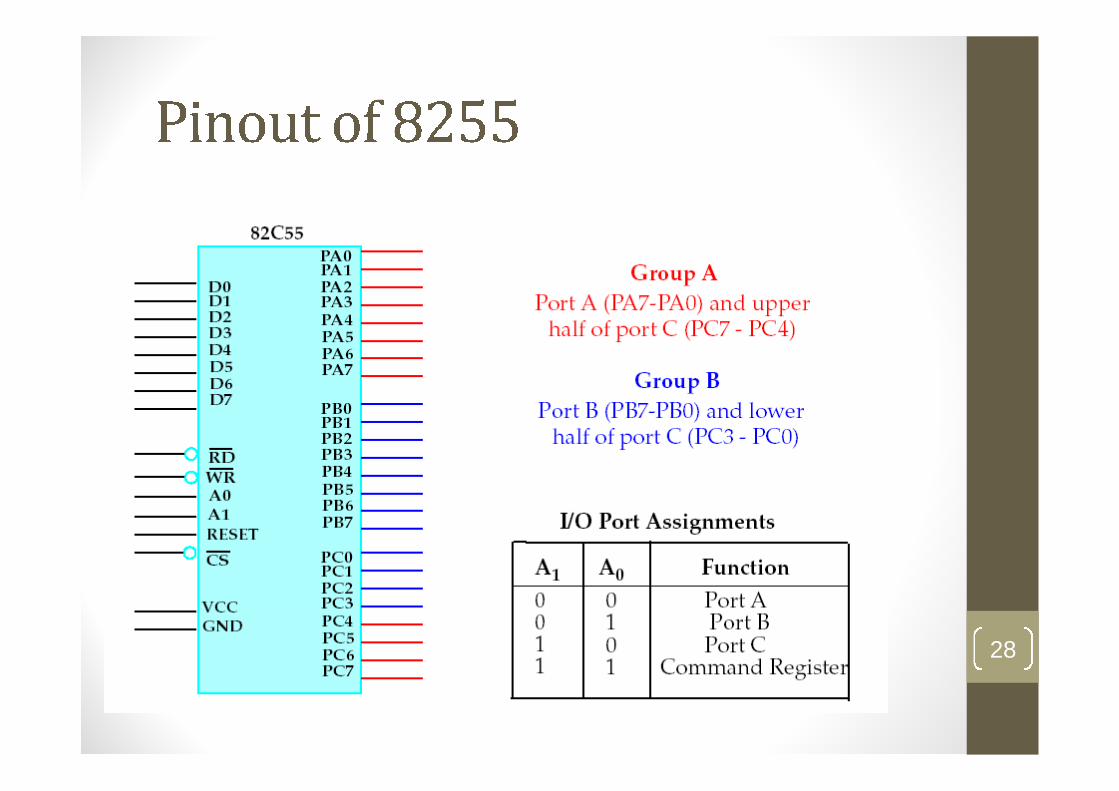
• 8255 - Widely used I/O chip• 40 pins
• Provides 3 eight bit ports PA, PB and PC
• Port PC can be used as two 4 bit ports PCL and PCU
• Ports have handshaking ability
• Two address lines A0, A1 and a Chip select CS• Address space of 4 bytes
• 00b selects Port A
• 01b selects Port B
• 10b selects Port C
• 11b selects an internal control register• Read only.
27
28
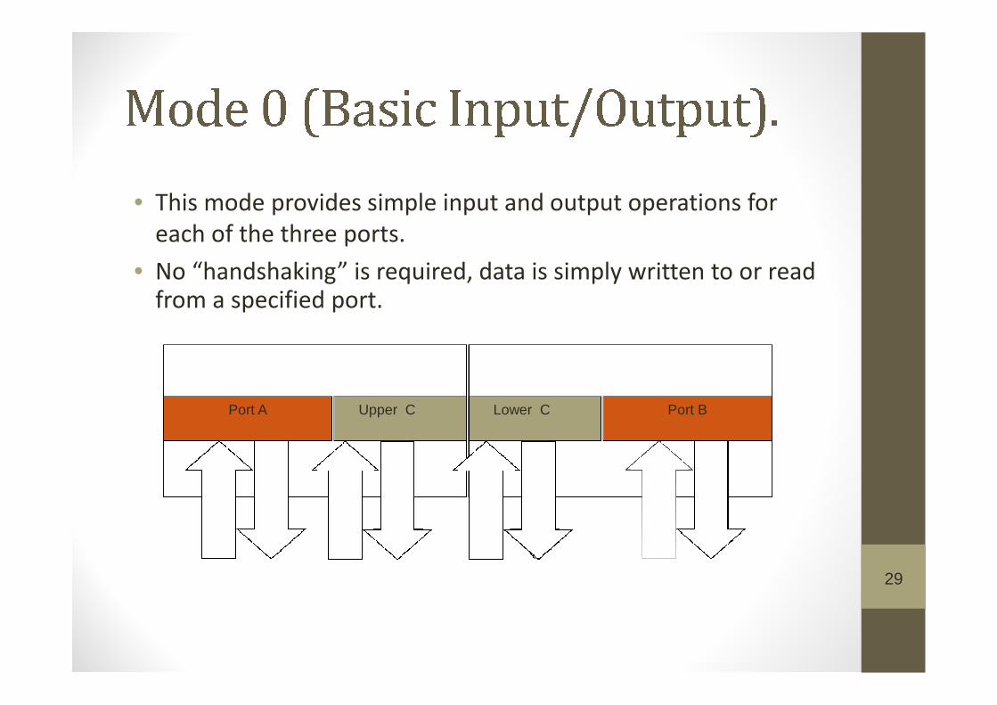
Port A Upper C Port BLower C
29
• This mode provides simple input and output operations foreach of the three ports.
• No “handshaking” is required, data is simply written to or readfrom a specified port.
30
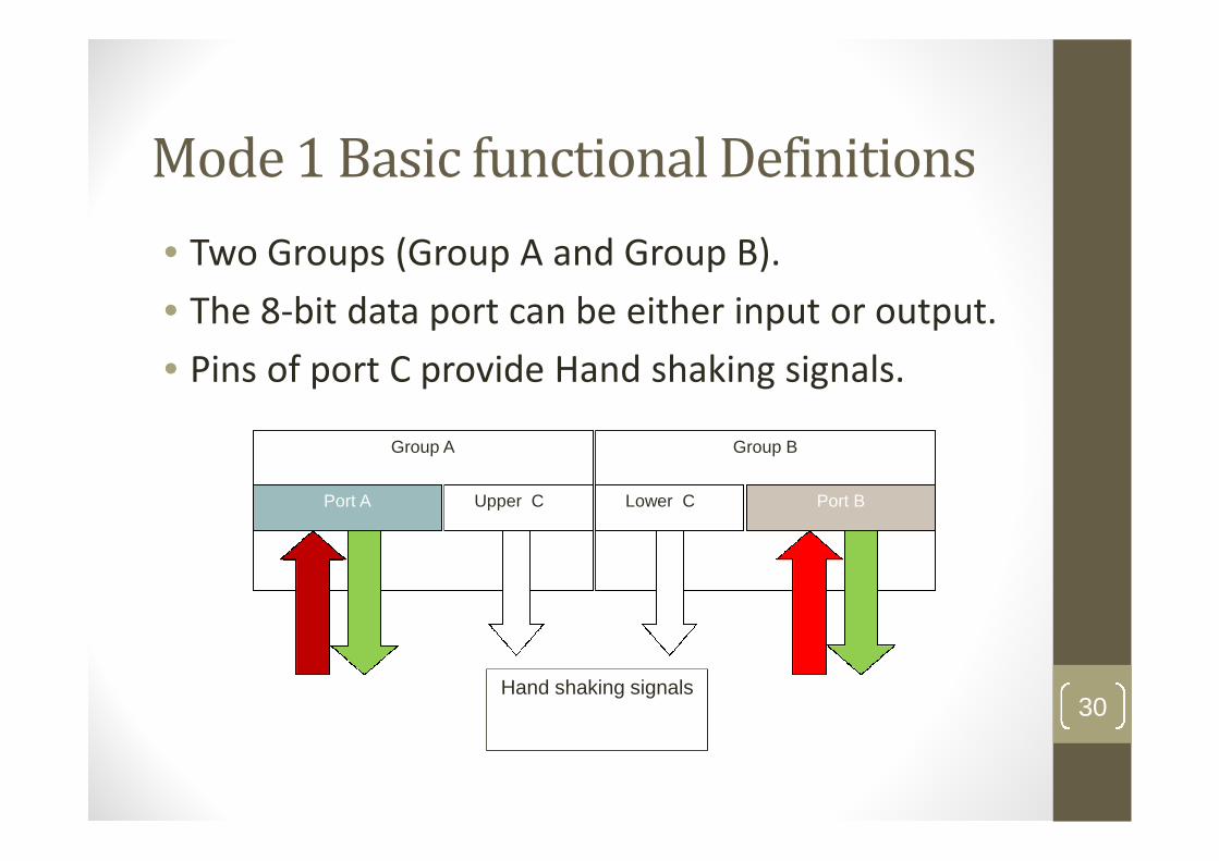
Mode 1 Basic functional Definitions
• Two Groups (Group A and Group B).
• The 8-bit data port can be either input or output.
• Pins of port C provide Hand shaking signals.
Group BGroup A
Port A Upper C Port BLower C
Hand shaking signals
31
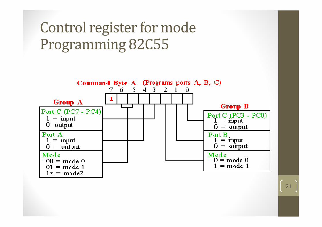
Control register for modeProgramming 82C55
32
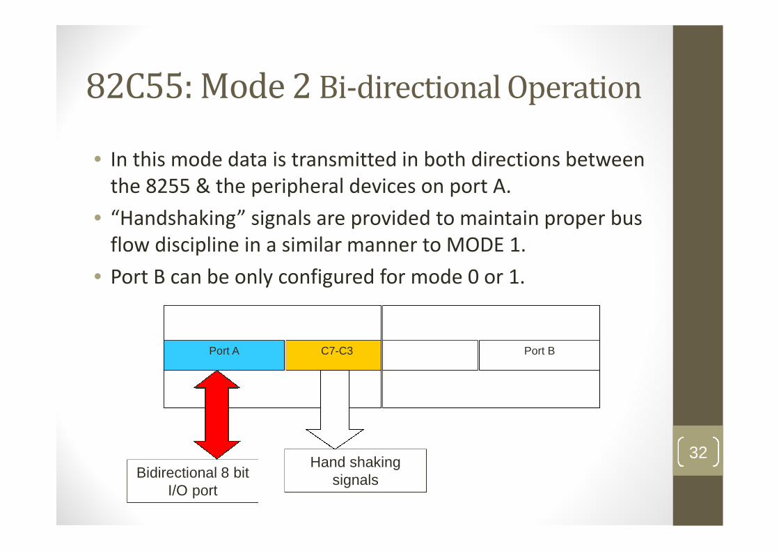
82C55: Mode 2 Bi-directional Operation
• In this mode data is transmitted in both directions betweenthe 8255 & the peripheral devices on port A.
• “Handshaking” signals are provided to maintain proper busflow discipline in a similar manner to MODE 1.
• Port B can be only configured for mode 0 or 1.
Port A C7-C3 Port B
Hand shakingsignalsBidirectional 8 bit
I/O port
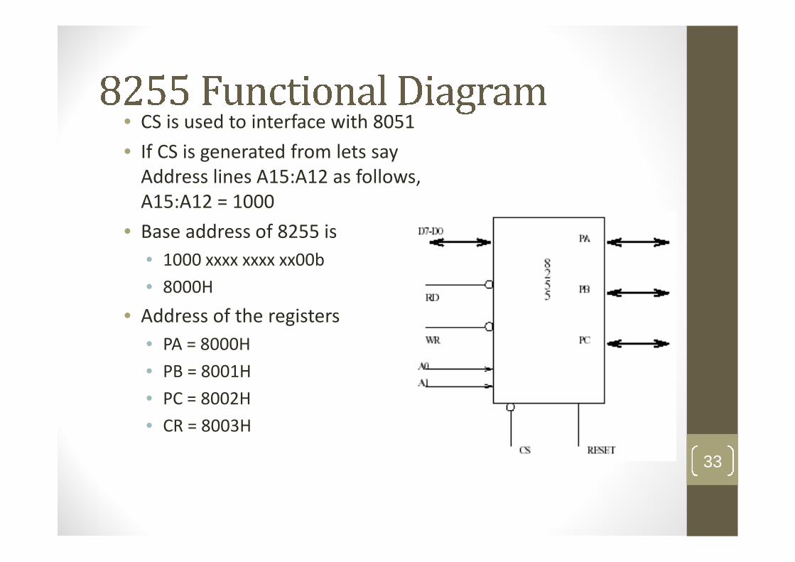
• CS is used to interface with 8051
• If CS is generated from lets sayAddress lines A15:A12 as follows,A15:A12 = 1000
• Base address of 8255 is
• 1000 xxxx xxxx xx00b
• 8000H
• Address of the registers
• PA = 8000H
• PB = 8001H
• PC = 8002H
• CR = 8003H
33
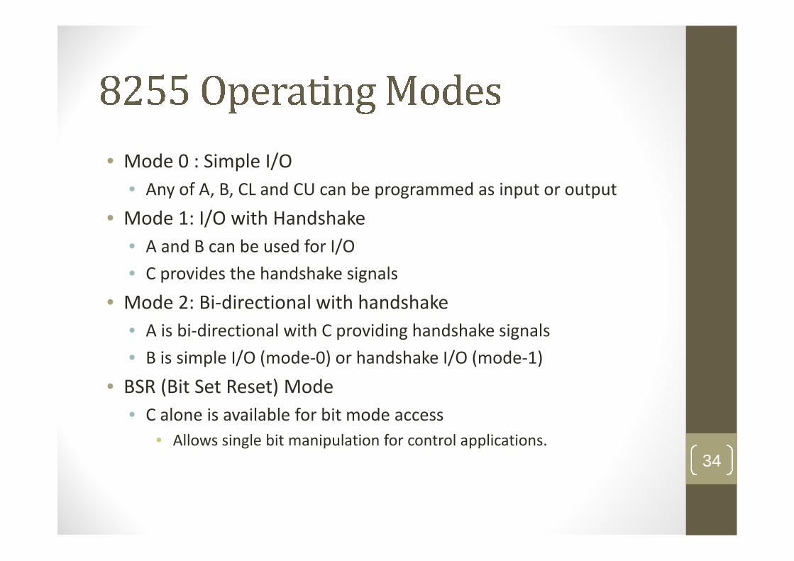
• Mode 0 : Simple I/O
• Any of A, B, CL and CU can be programmed as input or output
• Mode 1: I/O with Handshake
• A and B can be used for I/O
• C provides the handshake signals
• Mode 2: Bi-directional with handshake
• A is bi-directional with C providing handshake signals
• B is simple I/O (mode-0) or handshake I/O (mode-1)
• BSR (Bit Set Reset) Mode
• C alone is available for bit mode access
• Allows single bit manipulation for control applications.34
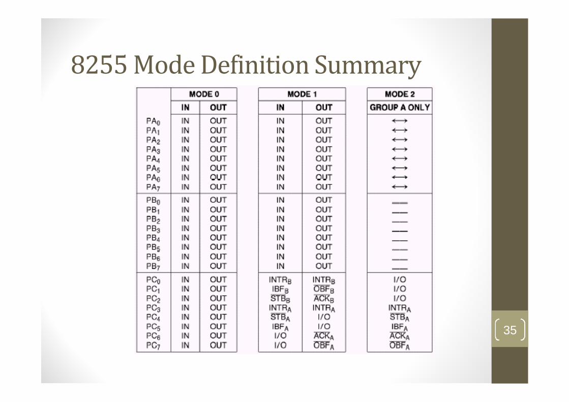
8255 Mode Definition Summary
35
• Configured by writing a control-word in CR register
• CR definition• D7 : 1I/O mode, 0 BSR
• D6,D5 : Mode selection for A and CU• 00 Mode0, 01 Mode1, 1x Mode2
• D4 : Port A control• 1 A input, 0 A output
• D3 : Port CU control• 1 CU input, 0 CU output
• D2 : Port B Mode selection• 0 B is in mode 0, 1 B is in mode 1
• D1 : Port B control• 1 B input, 0 B output
• D0 : Port CL control• 1 CL input, 0 CL output
• Refer to 8255 datasheet for additional options36
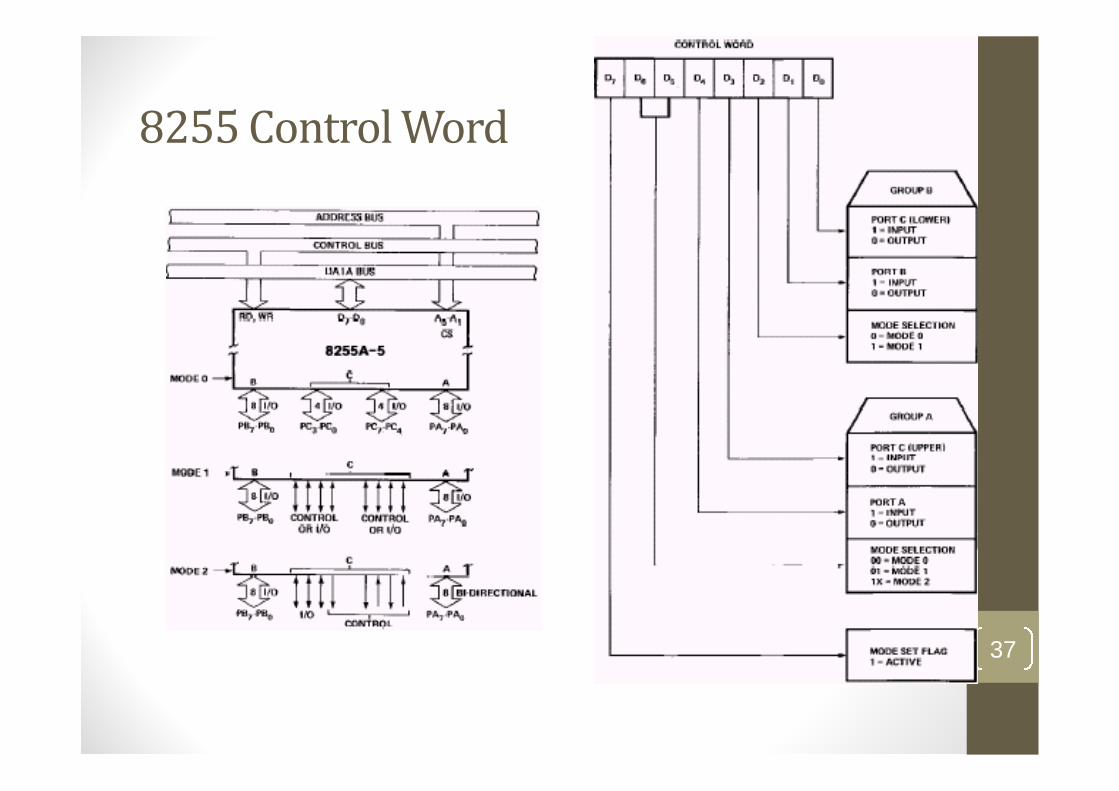
8255 Control Word
37
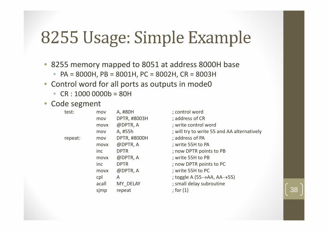
• 8255 memory mapped to 8051 at address 8000H base• PA = 8000H, PB = 8001H, PC = 8002H, CR = 8003H
• Control word for all ports as outputs in mode0• CR : 1000 0000b = 80H
• Code segmenttest: mov A, #80H ; control word
mov DPTR, #8003H ; address of CRmovx @DPTR, A ; write control wordmov A, #55h ; will try to write 55 and AA alternatively
repeat: mov DPTR, #8000H ; address of PAmovx @DPTR, A ; write 55H to PAinc DPTR ; now DPTR points to PBmovx @DPTR, A ; write 55H to PBinc DPTR ; now DPTR points to PCmovx @DPTR, A ; write 55H to PCcpl A ; toggle A (55AA, AA55)acall MY_DELAY ; small delay subroutinesjmp repeat ; for (1) 38
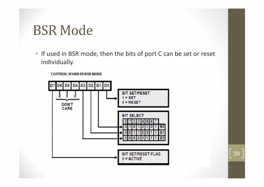
• If used in BSR mode, then the bits of port C can be set or resetindividually.
39