md0362 defibrillator monitor
TRANSCRIPT

U.S. ARMY MEDICAL DEPARTMENT CENTER AND SCHOOL FORT SAM HOUSTON, TEXAS 78234-6100
DEFIBRILLATOR/ MONITOR
SUBCOURSE MD0362 EDITION 100

DEVELOPMENT This subcourse is approved for resident and correspondence course instruction. It reflects the current thought of the Academy of Health Sciences and conforms to printed Department of the Army doctrine as closely as currently possible. Development and progress render such doctrine continuously subject to change.
ADMINISTRATION Students who desire credit hours for this correspondence subcourse must enroll in the subcourse. Application for enrollment should be made at the Internet website: http://www.atrrs.army.mil. You can access the course catalog in the upper right corner. Enter School Code 555 for medical correspondence courses. Copy down the course number and title. To apply for enrollment, return to the main ATRRS screen and scroll down the right side for ATRRS Channels. Click on SELF DEVELOPMENT to open the application; then follow the on-screen instructions. For comments or questions regarding enrollment, student records, or examination shipments, contact the Nonresident Instruction Branch at DSN 471-5877, commercial (210) 221-5877, toll-free 1-800-344-2380; fax: 210-221-4012 or DSN 471-4012, e-mail [email protected], or write to: NONRESIDENT INSTRUCTION BRANCH AMEDDC&S ATTN: MCCS-HSN 2105 11TH STREET SUITE 4191 FORT SAM HOUSTON TX 78234-5064
Be sure your social security number is on all correspondence sent to the Academy of Health Sciences.
CLARIFICATION OF TERMINOLOGY When used in this publication, words such as "he," "him," "his," and "men" 'are intended to include both the masculine and feminine genders, unless specifically stated otherwise or when obvious in context.
USE OF PROPRIETARY NAMES The initial letters of the names of some products may be capitalized in this subcourse. Such names are proprietary names, that is, brand names or trademarks. Proprietary names have been used in this subcourse only to make it a more effective learning aid. The use of any name, proprietary or otherwise, should not be interpreted as endorsement, deprecation, or criticism of a product; nor should such use be considered to interpret the validity of proprietary rights in a name, whether it is registered or not.

MD0362 i
TABLE OF CONTENTS Lesson Paragraphs INTRODUCTION 1 SERVICE PROCEDURES Section I. Preventive Maintenance Checks and Services (PMCS) ................................................................... 1-1 -- 1-3 Section II. Calibration and Verification .................................... 1-4 -- 1-8 Exercises 2 MALFUNCTIONS AND DEFECTIVE MODULES Section I. Isolate Malfunctions to Module Level ...................... 2-1 -- 2-6 Section II. Remove and Replace Defective Modules ............... 2-7 -- 2-9 Exercises APPENDIX A. Monitor Board Schematic--M 1 of 6 APPENDIX B. Monitor Board Schematic--M 2 of 6 APPENDIX C. Monitor Board Schematic--M 3 of 6 APPENDIX D. Monitor Board Schematic--M 4 of 6 APPENDIX E. Monitor Board Schematic--M 5 of 6 APPENDIX F. Monitor Board Schematic--M 6 of 6 APPENDIX G. Defibrillator Schematic--D 1 of 3 APPENDIX H. Defibrillator Schematic--D 2 of 3 APPENDIX I. Defibrillator Schematic--D 3 of 3

MD0362 ii
CORRESPONDENCE COURSE OF THE U.S. ARMY MEDICAL DEPARTMENT CENTER AND SCHOOL
SUBCOURSE MD0362
DEFIBRILLATOR/MONITOR
INTRODUCTION
In this subcourse, you will learn how to service and repair the Medical Research Laboratories (MRL) Porta Pak 90 defibrillator/monitor. This system is an extremely portable, full-function electrocardiograph (ECG) monitor/defibrillator. It can be used as an emergency, bedside, office surgery, or 12-lead diagnostic ECG monitor/recorder. You should have the monitor and defibrillator schematics in the appendixes (A through I) available while taking this entire subcourse. Refer to them as needed. Subcourse Components: This subcourse consists of 2 lessons and 9 appendixes as follows:
Lesson 1, Service Procedures.
Lesson 2, Malfunctions and Defective Modules.
Appendix A, Monitor Board Schematic--M 1 of 6.
Appendix B, Monitor Board Schematic--M 2 of 6.
Appendix C, Monitor Board Schematic--M 3 of 6.
Appendix D, Monitor Board Schematic--M 4 of 6.
Appendix E, Monitor Board Schematic--M 5 of 6.
Appendix F, Monitor Board Schematic--M 5 of 6.
Appendix G, Defibrillator Schematic--D 1 of 3.
Appendix H, Defibrillator Schematic--D 2 of 3.
Appendix I, Defibrillator Schematic--D 3 of 3.

MD0362 iii
Credit Awarded: Upon successful completion of the examination for this subcourse, you will be awarded 5 credit hours. To receive credit hours, you must be officially enrolled and complete an examination furnished by the Nonresident Instruction Branch at Fort Sam Houston, Texas. You can enroll by going to the web site http://atrrs.army.mil and enrolling under "Self Development" (School Code 555). A listing of correspondence courses and subcourses available through the Nonresident Instruction Section is found in Chapter 4 of DA Pamphlet 350-59, Army Correspondence Course Program Catalog. The DA PAM is available at the following website: http://www.usapa.army.mil/pdffiles/p350-59.pdf.

MD0362 1-1
LESSON ASSIGNMENT LESSON 1 Service Procedures. TEXT ASSIGNMENT Paragraphs 1-1 through 1-8. TASKS TAUGHT Perform PMCS on the Defibrillator/Monitor. Perform Calibration/Verification of the Defibrillator/Monitor. LESSON OBJECTIVES When you have completed this lesson, you should be able to: 1-1. Identify controls and status indicators on the defibrillator/monitor. 1-2. Perform a visual check. 1-3. Inspect the printed circuit board surfaces. 1-4. Access the main circuit board. 1-5. Perform an operational check on the defibrillator. 1-6. Perform calibration procedures. SUGGESTION Work the lesson exercises at the end of this lesson before beginning the next lesson. These exercises will help you accomplish the lesson objectives.

LESSON 1
SERVICE PROCEDURES
Section I. PREVENTIVE MAINTENANCE CHECKS AND SERVICES 1-1. GENERAL You must conduct periodic preventive maintenance checks and services (PMCS) of the Medical Research Laboratories (MRL) Porta Pak 90 defibrillator/monitor to ensure its continued operation. 1-2. CONTROLS AND STATUS INDICATOR CONTROLS Review the functions of the following controls and status indicators to ensure that you understand their purpose and how they function. Refer to figures 1-1 through 1-6. NOTE: The numbers in parenthesis correspond to the numbers in figures 1-1 through 1-6. a. Controls and Status Indicators for the Monitor. Refer to figure 1-1 for paragraphs (1) through (11). (1) Power control (1). The power control is the green push button switch for the main power to the monitor module. The power light is lit when the unit is on. When the monitor module is connected to the direct current (dc) defibrillator, turn the monitor on by depressing the defibrillator power switch. This is done to save operator time in an emergency situation. (2) Electrocardiograph monitor display (2). The nonfade electrocardiograph (ECG) display moves from right to left. (3) Quasi-Random Signal volume control (3). Turn the Quasi-Random Signal (QRS) volume control (3)switch clockwise to increase the volume of the systole beeper. For a 1 millivolt (mv) signal, push the switch and release it to activate the calibration signal on the ECG monitor and chart recorder. (4) Electrocardiograph size control (4). Turn the control clockwise to increase the amplitude. Push the button to hold or freeze the trace on the monitor scope. (5) Heart rate alarm control (5). Two rotary switches control the setting of the heart rate alarm limits. Turn the controls counter clockwise for low and clockwise for high. The Hi control provides a range of 100 to 240 beats per minute (bpm) and OFF. The Lo control provides a range of 30 to 100bpm, and OFF. When the alarm limits are exceeded, a steady tone is activated. When the chart recorder switch is in the AUTO mode, the chart recorder starts automatically and runs for 15 seconds. To deactivate the alarm system, turn both controls to OFF.
MD0362 1-2

MD0362 1-3
Figure 1-1. Monitor controls and status indicators.
(6) Heart rate display (6). The patient's heart rate is displayed from 30 to 300 bpm. (7) Chart recorder control switch (7). The four modes of control are: OFF, automatic (AUTO), DELAY, and diagnostic (DIAG). (a) OFF--The chart recorder is inactive. (b) AUTO--The chart recorder is in standby condition and will run for 15 seconds, including 6 seconds of memory information, when: (1) the alarm limits are exceeded and/or (2) the defibrillator is fired. (c) DELAY--The chart recorder will run continuously, printing 6 seconds behind what is displayed on the CRT monitor (ECG memory information). (d) DIAG--The chart recorder will run continuously at a diagnostic frequency response of .05 hertz per second (Hz) to 100Hz. The DIAG setting provides diagnostic quality for 12 lead ECG applications. (8) Lead select control (8). Turn the control clockwise to select ECG input from paddles, Lead I, II, III, AVR, AVL, AVF, or V.

MD0362 1-4
NOTE: The monitor and defibrillator modules must be interconnected and the defibrillator module turned on for paddle pick-up monitoring. (9) Chart recorder (9). The chart recorder records on standard 40mm. (10) Battery charger indicator (10). The battery charger indicator is lit when battery power paks are being charged and the unit is plugged into an alternating current (ac) power source. (11) Battery level display (11). The meter displays the charge capacity in the BATTERY mode of the MRL battery power pak when unit is turned on. When the indicator is in the green area, the power pak is adequately charged. When the indicator is in the red area, the power pak should be recharged or exchanged for one fully charged immediately. (12) Patient connector (12). Refer to figure 1-2 for paragraphs (12) through (17). The patient connector accepts the three or five lead patient cable (6 pin AAMI Standard). (13) Power cord (13). For monitor and defibrillator interconnected operation, insert the monitor power cord into receptacle on the defibrillator module. You then insert the defibrillator power cord into grounded ac power source. (14) Fuse holder (14). The fuse holder holds the appropriate fuse for the line voltage selected. (15) Electrocardiograph output (15). The ECG output provides 1 volt (v) output for accessory equipment. (16) Voltage selector switch (16). Use the voltage selector switch to select proper voltage for 110v or 220v line power. (17) Monitor rear jack (17). The monitor rear jack is for monitor and defibrillator interconnected operation.

MD0362 1-5
Figure 1-2. Monitor back panel. b. Controls and Status Indicators for the Defibrillator. Refer to figure 1-3 for paragraphs (1) through (13).
Figure 1-3. Defibrillator controls and status indicators.

MD0362 1-6
(1) Power control (18). The power control is the green push button switch for main power to the defibrillator module. NOTE: When you depress the defibrillator power switch, it activates and deactivates the monitor while both modules are interconnected and both green power switches are in the OFF position. The power lamp will light on both units. The monitor and defibrillator modules may be turned on and off independently of each other. (2) Energy select switch (19). The energy select switch is an eight position rotary switch with the following selections: 5, 10, 20, 30, 50, 100, 200, and 360 joules of delivered energy. (3) Charge button (20). To charge the defibrillator, depress the yellow charge button on the console or APEX paddle. An intermittent tone will sound, the yellow charge switch will flash, and the yellow LED selected energy display will flash during the charge period. When fully charged, the charge button will show a steady light, the tone will be constant, and the yellow selected energy display will remain lit. (4) Sync button (21). When you depress the sync button, the sync is activated, and the white push button is lit. The sinc mode automatically turns off when the disarm button is pressed, when the sync switch and defibrillator are turned off and the defibrillator is fired. NOTE: The defibrillator module must be interconnected to the monitor for synchronized operation. After a synchronized discharge, the sinc mode is automatically turned off. (5) Disarm button (22). Pressing the red disarm push button discharges the defibrillator internally, but maintains power to defibrillator module. (6) Internal fire button (23). The blue internal fire push button discharges the defibrillator for internal defibrillation. NOTE: Internal energy selections are automatically limited to 50 joules (j) or less. A higher than 50j energy selection, with the internal paddles connected will show an "Err" (error) message displayed on the selected energy meter, and the defibrillator will not charge. (7) Battery charger indicator (24). The battery charger indicator is lit when the battery paks are being charged and the unit is plugged into the ac power source.

MD0362 1-7
(8) Battery level indicator (25). The battery level meter displays the charge capacity of battery power pak when units are turned on in the BATTERY mode. When the indicator is in the green area, the power pak is adequately charged. When the indicator is in the red area, the power pak should be recharged or exchanged for one fully charged immediately. (9) Selected energy display (26). The digital display of selected energy level LED numerals will flash during the defibrillator charge. They will glow steadily when the defibrillator is fully charged. "Err" (error) will be displayed when the paddles are not plugged in or higher than 50j are selected with the internal paddles connected. (10) Delivered energy display (27). There is a digital display of the precise delivered energy into the test load circuit or to the patient at all levels (+/-15 percent) upon defibrillator discharge. (11) Sternum button (28). The sternum defibrillator paddle has one red discharge button. It should be positioned on the sternum for the paddle pick-up ECG monitor display. (12) Apex button (29). The apex defibrillator paddle has one red discharge button and one yellow defibrillator remote charge button. Depressing the yellow charge button will activate the charging cycle. The charge button flashes during the charging cycle and glows steadily when the defibrillator is ready to fire. The paddle should be positioned near the cardiac apex for paddle pick-up. NOTE: Depress both red fire buttons simultaneously to discharge the defibrillator (13) Test load display (30). A test load of 50 ohms is provided to test the defibrillation charge at any selected energy level. The delivered energy (±15 percent) is displayed by the delivered energy meter. (14) Defibrillator power cord (31). Refer to figure 1-4 for paragraphs (14) through (18). The defibrillator power cord provides ac power to the interconnected defibrillator and monitor modules when it is connected to a grounded ac power source. (15) Power cord receptacle (32). The power cord receptacle is used to receive the monitor module power cord when the defibrillator power cord is used to provide line power and a battery charge for both modules. (16) Paddle cord connector receptacle (33). The paddle cord connector receptacle receives the external, internal and/or anterior/posterior paddle cord connector. Line up the yellow guide markings to facilitate connection.

MD0362 1-8
Figure 1-4. Defibrillator back panel. (17) Voltage selector switch (34). Refer to figure 1-5 for a more detailed view. Use the voltage selector switch to select proper voltage for 110v or 220v line power. (18) Fuse holder (35). The fuse holder holds the appropriate fuse for the line voltage selected.
Figure 1-5. Voltage selector switch. 1-3. PERFORM A VISUAL CHECK ON DEFIBRILLATOR AND MONITOR Now that you know the functions of the controls and status indicators, you can perform the inspections and tests to ensure the readiness and optimum working condition of your MRL Porta Pak 90. Be sure to follow the safety precautions when accessing the monitor and defibrillator main circuit board. a. General Safety Precautions. Perform the following before disassembling the monitor: NOTE: The defibrillator has 1350v. (1) Turn off the monitor.

MD0362 1-9
(2) Disconnect the monitor from the ac line. (3) Remove the patient cable. (4) Remove the output cable. b. Access the Monitor Main Circuit Board. (1) Remove the two front screws holding the base to the monitor chassis (figure 1-6). (2) Loosen the two rear screws to function as a hinge for easy access to the circuit boards. (3) Rotate the monitor into an upright position (figure 1-7). Figure 1-6. Monitor circuit board access. Figure 1-7. Monitor chassis in fully open position. c. General Safety Precautions. Perform the following before disassembling the defibrillator/cardioscope: (1) Turn off the defibrillator module. (2) Remove the line cord. (3) Remove the paddle set.

MD0362 1-10
d. Access the Defibrillator Main Circuit Board. (1) Remove the defibrillator/cardioscope from the Model Porta Pak 90 case to access the defibrillator main circuit board components. (a) Remove the defibrillator cover plate as a single unit by leaving the three screws (refer to arrows in figure 1-8) on the panel installed and removing the remaining eight screws. (b) Reach through the paddle set connector opening (at the rear of the defibrillator) and, with your other hand at the front panel edge, carefully lift up the defibrillator cover plates.
Figure 1-8. Defibrillator cover plate removal.
(2) Inspect all external surfaces. (a) Check for physical damage. (b) Check for breakage. (c) Check for loose or dirty contacts. (d) Check for missing components. (3) Inspect the printed circuit board surfaces. Refer to figure 1-9. (a) Check for discoloration. (b) Check for cracks and breaks. (c) Check for warping.

MD0362 1-11
Figure 1-9. Defibrillator circuit board. (4) Inspect all assemblies for burnt or loose components. (5) Inspect all chassis and panel mounted components for looseness, breakage, loose contacts, or loose conductors. (6) Inspect for disconnected, broken, cut, loose, or frayed wires and cables. (7) Inspect the patient paddles for pitted conditions and excess buildup of electrolyte paste. (8) Inspect the patient cables for discoloration, broken insulation, and loose connectors. e. Perform an Operational Check on the Defibrillator. After performing visual checks and inspections, you perform the operational checks. Perform the checks daily or at each shift change. Refer to Figure 2-2 in lesson 2 for procedures to perform daily checks.

MD0362 1-12
f. General Safety Precautions. Ensure that the following precautions are followed when operating the defibrillator. (1) Select the proper voltage for either 110v or 220v. (2) Stand clear of the patient during defibrillation procedures. (3) Do not use the MRL Porta Pak 90 defibrillator and cardiac monitor in the presence of anesthetics or flammable material. (4) Keep defibrillator paddles clean and dry when not in use. When preparing electrodes and during defibrillation procedures, exercise extreme care to prevent gel or any conductive material from forming a contact between the operator and the paddles. (5) Use only MRL patient cables or those that meet AAMI patient cable and connector standards.
WARNING
Pacemaker Patients. Rate meters may continue to count the pacemaker rate during some occurrences of cardiac arrest or some arrhythmias. Do not rely upon rate meter alarms. Keep pacemaker patients under close surveillance.
Section II. CALIBRATION AND VERIFICATION
1-4. CALIBRATE AND VERIFY THE POWER SUPPLY/DEFLECTION OF THE MONITOR In addition to PMCS, you are also responsible for performing calibration and verification procedures. In this section you will learn how to calibrate the MRL Porta Pak 90 to ensure its safe use during surgery. When you calibrate the defibrillator/monitor, you verify its output against a known standard. If the unit fails calibration, you must repair it before returning it to service. Refer to paragraph 1-3 for general safety precautions. a. Access the Monitor Main Circuit Board. To calibrate the monitor, you must access the main circuit board. Remove the monitor chassis from the base. Follow the procedures in paragraph 1-3.b. Rotate the monitor into an upright position (figure 1-10).
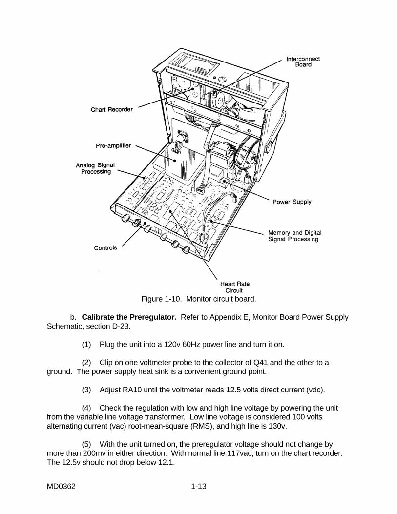
MD0362 1-13
Figure 1-10. Monitor circuit board.
b. Calibrate the Preregulator. Refer to Appendix E, Monitor Board Power Supply Schematic, section D-23. (1) Plug the unit into a 120v 60Hz power line and turn it on. (2) Clip on one voltmeter probe to the collector of Q41 and the other to a ground. The power supply heat sink is a convenient ground point. (3) Adjust RA10 until the voltmeter reads 12.5 volts direct current (vdc). (4) Check the regulation with low and high line voltage by powering the unit from the variable line voltage transformer. Low line voltage is considered 100 volts alternating current (vac) root-mean-square (RMS), and high line is 130v. (5) With the unit turned on, the preregulator voltage should not change by more than 200mv in either direction. With normal line 117vac, turn on the chart recorder. The 12.5v should not drop below 12.1.

MD0362 1-14
c. Check the Battery Charger (NiCad). Refer to Appendix E, Monitor Board Power Supply Schematic, section D-22. (1) Disconnect the battery from the charging circuit and substitute a resistive load of 75 ohms (± 5 percent). This load should have a power rating of approximately 5 watts (w). (2) Plug the unit into an outlet. The rest of the unit should remain turned off. (3) Place an milliampere (ma) meter in series with the 75 ohm load. Adjust RA2 until the meter reads 250ma. Short circuit the load for a few seconds at a time. The current should not increase by more than 70ma, showing correct action of the current regulator circuit. (4) Turn on the unit. With nominal line voltage (120v or 230v RMS), the charge current should not fall by more than 60ma. The voltage across the load resistor should be at least 14vdc with the unit turned off. A discharged NiCad battery in good condition should recover 100 percent of its charge in 14 hours at room temperature (approximately 70 degrees Fahrenheit). d. Check the Low Battery Shut-Off. Refer to Appendix E, Monitor Board Power Supply Schematic, section E-24. (1) Unplug the unit from line. (2) Remove the battery completely and connect, in its place, a variable dc power supply from 9v to 14v and 2 amps current capability. (3) Set the supply voltage to 12.0v. (4) Turn on the unit. (5) After the trace is stabilized, lower the voltage gradually until the unit shuts off. This should occur at 9.5v. If this is not the case, adjust RA16 (four-turn control) and repeat the procedure until the low voltage shut off is correct. (6) Check the hysterisis control by increasing the power supply voltage to 11.0v. Leave the monitor on/off switch on and allow the low voltage shut off to turn the unit off. The unit should not turn itself on below this voltage. e. Check the Overall Battery Current. (1) With the same set up as described under low battery shut off calibration, connect a dc ammeter (0-2A) in series with the positive lead of the power supply.

MD0362 1-15
(2) Adjust the voltage at the input terminals to the printed circuit board (pcb) to be 12.5v with the unit turned on, but the chart recorder turned off. (3) Apply a signal of 1mv, 60bpm from the ECG simulator to the patient cable input. The current taken from the supply should be 580ma or less, with small fluctuations in accordance with the heart rate display. When the chart recorder is turned on, this current should jump up 500ma. f. Calibrate the Battery Meter. Refer to Appendix E, Monitor Board Power Supply Schematic, section D-24. (1) The line or pointer of the moving coil meter should be at the intersection of the green and red areas with a supply voltage of 11.0v using the same general set up as for low battery shut off calibration. (2) This adjustment is performed by turning RA13 (four-turn control). g. Adjust the Horizontal Amplitude. Refer to Appendixes E, Monitor Board Power Supply Schematic, section C-24. (1) Using a 60bpm heart rate, adjust the distance between QRS complexes to 25mm by adjusting R241 (one-turn control) in the center portion of the screen. (2) If the trace is not covering the full width of the screen, rotate one or both magnets located on the back of the deflection yoke assembly. If some non-linearity seems to be present, you must corrected this by using the horizontal linearity controls R216 and R217 located on the main PCB. h. Calibrate the Vertical Amplitude. Refer to Appendix E, Monitor Board Power Supply Schematic, section C-22. (1) Use the same general set up as for horizontal deflection amplitude. Operate the unit with an ECG simulator 1mv output. (2) Set the manual amplitude control to the center position and adjust the actual signal amplitude on the CRT to a high of 20mm by turning control R231 (one-turn control). NOTE: The horizontal and vertical deflection controls affect only the display on the CRT. Their settings do not affect the chart recorder or any of the auxiliary outputs.

MD0362 1-16
i. Adjust the Brightness and Focus. Refer to Appendix E, Monitor Board Power Supply Schematic, sections A-23 and B-24. (1) Start with a brightness setting by adjusting R85, which gives an acceptable trace reading with the light filter in position. Next, turn R80 (one-turn control) focus adjust to the best trace definition possible, both vertical and horizontal, since this CRT doesn't need astigmatism adjustment. (2) If the trace is getting too bright once you correct focus, reduce the brightness by turning R85 to a more suitable value. If these adjustments are not turning out satisfactorily, check the fixed dc voltage on pins 2 and 6 of the CRT (+360v approximately) and also the high voltage on the second anode of the CRT. (3) Since this electrode is taking only about 5.0 microamperes under normal brightness condition, any additional load by the voltmeter probe has to be kept as low as possible. In practice, we found that a 1000 meg ohm (meg) probe introduces a minus error of about 6 percent without disturbing the filtering. So a reading of 4.9 kilovolt (kv) with the probe means that the true anode voltage is close to 5.1kv. NOTE: Discharging the high voltage through short-circuit may cause permanent damage to the caper military occupational specialty (CMOS) circuits. Use a 1meg, 1w resistor to discharge the high voltage. NOTE: Do not operate the CRT below 4.0kv or above 6.5kv. 1-5. CALIBRATE THE GROUNDED ANALOG AMPLIFIER In this section, it is assumed that the power supply assembly and the preamplifiers (patent cable and paddle) are already completely adjusted. Perform the following procedures to calibrate the grounded analog amplifier. a. Calibrate the Monitor. Refer to Appendix A, Monitor Board Pre-Amp Schematic, section C-4. (1) Adjust the dc offset control, R33, so as to present 0v to 0.02v positive at pin 9 of the voltage to frequency converter. This voltage should never read negative. (2) This calibration should be done with no input signal or all patient leads shorted together. b. Calibrate the FM Detector. Refer to Appendix B, Monitor Board Analog Schematic, section C-6. (1) With lead 1 position RA, LA, and LL shorted together, connect the voltmeter to pin 7 of U101 and adjust R102 (four-turn control) to the lowest possible dc offset voltage as shown by the digital voltmeter.

MD0362 1-17
(2) This calibration should be performed after five minutes of a warm up interval to ensure tracking between the voltage to frequency converter and the phase lock loop (PLL). c. Calibrate the Manual Size Control and 1mv Calibration Chart Recorder. Refer to Appendix B, Monitor Board Analog Schematic, sections B-7 and B-9. (1) Be sure the ECG simulator and lead selector switch are in the lead 1 configuration, the simulator output is exactly 1.0mv with 60 to 80bpm, and the size control is in its center position. (2) Turn the unit on and wait five minutes for stabilization. Depress the 1mv calibration button several times. A positive going pulse should appear on the CRT with sharp rising and falling edges. (3) By adjusting R111 (one-turn control), make the positive deflection above the base line exactly the same height as the peak of the QRS complex of the incoming signal. (4) Now switch the chart recorder selector to DIAGNOSTIC. (5) Adjust R138 (four-turn control) so as to obtain exactly 20mm of pen deflection at the peak of the QRS complex. (6) Push the 1mv calibration button for 1/2 second at a time. During each interval the button is pushed, the input signal is removed, and a square pulse appears on the chart which should have the same amplitude (20mm) as the QRS complex. If you notice a deviation of more than 2mm between the amplitude of both signals, check the frequency response of the chart recorder. It may have changed from the original settings because of differences in paper or pen pressure. d. Calibrate the Display and Chart Recorder Amplitude. Refer to Appendix B, Monitor Board Analog Schematic, sections B-8, B-9, and B10. (1) Reconnect the ECG simulator to the input. (2) Adjust the output to 1mv and 60bpm. (3) Turn the size control to its center position. (4) Now turn R123 until the oscilloscope connected to pin 14 of U102 shows a signal of 1.5v P/P. Disregard the superimposed dc voltage. If there is a difference in amplitude between the signal on the chart recorder and the CRT in diagnostic operation, R138 has to be adjusted until both are identical.

MD0362 1-18
(5) Switch the chart recorder mode selector to DELAYED. (6) Adjust R141 until the signal amplitude on the chart recorder and the CRT are similar in amplitude. Remember that the signal recorded on the chart is always five seconds delayed with respect to the CRT display in this mode of operation. e. Calibrate and Check the Quasi-Random Signal Sensitivity Sensitivity. Refer to Appendix B, Monitor Board Analog Schematic, section D-8. (1) Turn down the output of the ECG simulator to 0.4mv, 60bpm, Lead 1 configuration. (2) Adjust R145 (one-turn control) to a point where the system just recognizes a QRS complex. (3) Now switch the ECG simulator to 5.0mv output. (4) Reduce the size to 20mm. No double triggering should be noticeable. (5) Switch the amplitude back to 1.0mv and the rate to 240bpm. No beats should be missing. (6) Now lower the rate to 30bpm. The recognition should be correct. f. Check the Overall Signal to Noise. (1) Operate the unit in Lead 1. Allow a few minutes for stabilization. (2) Apply a 20 microvolt signal from the output of the ECG simulator to the patient cable input. The heart rate should be 60bpm. The QRS complexes should still be recognizable as little bumps about twice in size than the width of the base line trace. g. Check the Synchronizer. (1) You can make this check with or without the defibrillator connected and turned ON (not charged up and sync switch engaged). A marker pulse should appear on the CRT screen each time a QRS complex appears at the patient cable input. (2) Switch to paddle pick-up, and the marker pulse is canceled out, even if a QRS signal is applied to the paddles.

MD0362 1-19
(3) Another way of testing without the defibrillator is to apply an external 12 dc power source to pin 4 of J3 with the positive through a 1 kilo (k) resistor to pin 4 of J3, and the negative to the ground. As soon as the external source is turned on, the marker pulse is present. By observing the signal at pin 4 of J3 on the oscilloscope, a negative-going pulse of about 4.0 volt amplitude and 5.0 milliseconds (msec) duration should appear for each QRS recognition. The pulse should not be present during the time the hold button is depressed. h. Check the Paddle Preamplifier Input. (1) Select paddle pick-up mode and apply a 10.0Hz 1.0v P/P signal from the low frequency audio generator to pin 6 of J3 and pin 11 (ground) of J3. (2) A clean recorder sine wave should be displayed on the CRT and on the chart records when in the delayed mode of operation. This signal should diminish rapidly in amplitude above 30Hz. i. Calibrate the Heart Rate Meter and Alarm. Refer to Appendix D, Monitor Board Heart Rate Meter Schematic, sections C-17, C-18, and D-18. (1) Since the heart rate meter takes its signal from the QRS recognizer, it is necessary to verify that the recognizer circuit functions properly. Calibrate the reference voltage which appears at TP1 pin 1 to exactly 1.000v +\-1.0mv by turning R186. (2) Drive the patient cable input with an ECG simulator at 1.0mv and 240bpm. The following repetition rates of the signal have to be accurately known: 30, 60, and 240bpm, for this test. (3) Once the read out number has stabilized within 2 beats plus or minus, turn R190 (four-turn control) so as to obtain a read out of 240bpm, + or - 2bpm. (4) Now switch to 60bpm. The read out should stabilize at + or - 1bpm. After this test, switch to 30bpm. The read out should, again, stabilize at + or - 1bpm. NOTE: This concludes the calibration and verification of its linearity. Let us proceed to the heart rate alarm circuits. (5) Connect an oscilloscope probe between TP1 pin 3 and TP1 pin 4 (ground). An absolutely linear, positive ramp should appear at the repetition rate of four times per second, approximately, when the input to the unit is driven by an ECG signal of 240bpm. (6) Adjust R197 (one-turn control) until the peak value of the ramp is 4.0v in amplitude.

MD0362 1-20
(7) Go back to 60bpm. Turn the Hi limit set ON with the pointer facing 240bpm. Switch to 240bpm. After a few seconds, the alarm triggers, indicated by a loud continuous tone from the beeper. (8) Verify that the pointer of the knob is facing the number 240 on the front panel; loosen and reposition if necessary. (9) Now switch the input signal to 30bpm. After a few seconds, the unit goes out of alarm. Turn the Lo limit set on and advance clockwise until the pointer faces 30bpm. After stabilization, the alarm should sound. (10) Verify that the pointer knob faces the number 30 on the panel. (11) Switch the input signal to 60bpm. No alarm condition should be registered once the read-out reaches that figure. j. Adjust the Chart Recorder Timer. Refer to Appendix B, Monitor Board Analog Schematic, section E-7. (1) Switch the chart recorder mode selector to the AUTO position. (2) Create a Hi or Lo heart rate alarm condition by adjusting the repetition rate of the ECG simulator connected to the patient cable input. (3) The chart recorder should start as soon as the beeper signals an alarm condition. It should keep running for 15 seconds even if the alarm condition disappears before that interval and the signal displayed will be in the delayed mode. (4) The running time can be adjusted with R176 (one-turn control). With the chart recorder mode selector in the same position, connect the defibrillator and turn it on and charge up (any energy level). In the same instant the defibrillator is fired, the chart recorder starts running again for 15 seconds. The same action can be simulated by introducing a 12v positive-going pulse into pin 8 of J4, which is the defibrillator fire pulse input to the monitor. NOTE: This concludes the check and calibration procedure for the grounded analog section of the Porta Pak 90 monitor.

MD0362 1-21
1-6. CALIBRATE THE NONFADE CIRCUIT Perform the following procedures to calibrate the nonfade circuit. a. Check and Adjust the Linearity. Refer to Appendix E, Monitor Board Power Supply Schematic, sections C-23 and C-24. (1) Apply an ECG signal to the input of monitor. (2) Check the horizontal width for correct adjustment. (3) Adjust both linearity controls R216 and R217 for the best linearity of trace. b. Calibrate the Delayed Analog Signal. Refer to Appendix B, Monitor Board Analog Schematic, section D-10. (1) Apply an ECG signal to input of the monitor. (2) Adjust R141 for proper level on the chart recorder. 1-7. CALIBRATE THE DEFIBRILLATOR BOARD Perform the following procedures to calibrate the defibrillator board. CAUTION: Potentials of approximately 1.4kvdc are present on the defibrillator board. a. Calibrate the High Voltage. Refer to Appendix G, Porta Pak 90 Defibrillator Schematic, section C-10. (1) With a digital voltmeter (with appropriate attenuator for 1500vdc) connected at J1, pin 3 (-) and pin 5 (+), turn on the power. Be sure that the standard paddle set is connected at J10. (2) Select 200j energy level and activate the charge button. The meter should read 1170v when the ready light comes on. If not, then R111 should be slowly adjusted clockwise or counter clockwise until the voltage reads 1170v. (3) Press the disarm button and select energy levels progressively from 5j. Check the voltages. The voltages will all be within ± 2.0v if R111 was carefully set. Check for the following (table 1-1).

MD0362 1-22
ENERGY SETTING VOLTAGE Joules Volts 5 200 10 270 20 370 30 440 50 575 100 832 360 1355
Table 1-1. Energy setting and voltage.
(4) Next, with the aid of a defibrillator output tester, select 200j. Charge up the defibrillator and deliver energy to the tester. The output should be 200j. If not, adjust R112 clockwise or counter clockwise until exactly 200j are delivered. All other energy levels should be nominal ± 1j, except 360j, which will be 5j or a maximum deviation of 15 percent, whichever is greater. b. Adjust the Safety Dump Time-Out. Refer to Appendix G, Porta Pak 90 Defibrillator Schematic, section B-4. (1) The safety dump time-out is adjusted by R61 so that if the paddles are fired open circuit, the high voltage will be internally dumped in less than 40msec. (2) This can best be seen on the oscilloscope by observing the discharge across R67, the 1k 25w resistor. In essence, this is viewing the pulse from paddle to paddle. This must be done using a scope with a high voltage probe capable of 2000v with the scope in the triggered sweep mode. c. Adjust the Battery Meter. Refer to Appendix G, Porta Pak 90 Defibrillator Schematic, section B-9. (1) With the battery disconnected from J4, connect a variable dc power supply to J4 with the voltage adjusted to 11.0v. (2) Turn on the power switch, but do not charge. (3) Adjust R198 so that the needle on the meter is on the line of transition between the red and green area of the meter face.

MD0362 1-23
d. Adjust the Low Battery Cut-off Circuit. Refer to Appendix G, Porta Pak 90 Defibrillator Schematic, section B-10. (1) With the power supply connected to J4 as for the battery meter (see paragraph f(3)), close the power switch and observe it light up. (2) Adjust R113 to a point where the light just turns off at 9.5v. This is the proper setting for the low battery cut-off. e. Adjust the Battery Charger (NiCad). Refer to Appendix G, Porta Pak 90 Defibrillator Schematic, section B-10. (1) Disconnect the battery from the charging circuit and substitute a resistive load of 75 ohms (± 5 percent). This load should have a power rating of approximately 5w. (2) Plug the unit into an outlet. The rest of the unit should remain turned off. (3) Adjust RA2 until an ma meter in series with the 75 ohm load reads 250ma. Short circuit the load for a few seconds at a time. The current should not increase by more than 70ma, showing correct action of the current regulator circuit. (4) Turn on the unit. With nominal line voltage (120v or 230v RMS), the charge current through the load should not fall by more than 60ma. The voltage across the load resistor should be at least 14vdc with the unit turned off. A discharged NiCad battery in good condition should recover 100 percent of its charge in 14 hours at room temperature (approximately 70 degrees Fahrenheit). f. Calibrate the Delivered Energy. Refer to Appendix G, Porta Pak 90 Defibrillator Schematic, section C-4. CAUTION: The power supplies and ground of this entire pcb may be as much as 1360vdc above ground potential of the rest of the unit. (1) Turn on the power switch; however, do not charge the defibrillator. Any calibration has to start with the reference voltage of the digital voltmeter. The voltage has to be exactly 1.000vdc between test points 1 and 2, connecting pin 37 of U38 to +5v of the on board supply. All segments of the three display digits should light up. Do not leave the system in this condition for more than 10 seconds. (2) Turn off the power switch. Wait a couple of seconds and turn it on again. The display should light up showing 000,001 is acceptable. If any significant reading appears, turn R160 (zero balance) until 000 is displayed each time the unit is turned on. NOTE: For the following steps, a defibrillator tester is needed with a standard load of
50.0 ohm.

MD0362 1-24
(3) Charge the defibrillator in the 360j position and fire it into the defibrillator tester and also take note of the reading on the display. Let us assume it reads 280j against 340j displayed on the defibrillator tester. (4) Repeat the operation at 30j setting. Let us assume the delivered energy reading is 22j against 30j on the defibrillator tester. (5) Comparing the readings of low and high energy, both appear low. This is an indication that the calibration control (R132) needs adjustment. (6) Set the energy selector of the defibrillator to 200j and charge and fire into the defibrillator tester. During the display time (eight seconds), adjust R132 until a close reading to that of the defibrillator tester is obtained. (7) After completion of the 200j adjustment, check readings at 30j and 360j. They should fall within ± 15 percent +1 digit of the defibrillator tester indication. NOTE: Let us assume now a different condition exists: Readings on the high energy levels are above or below the error limit. (8) Keep the energy setting of the defibrillator at the extreme where the readings show the worst error. (9) Charge and fire into the defibrillator tester repeatedly. Between firings, adjust R140 a 1/8th turn at a time until your error seems to be corrected. (10) Check the voltmeter calibration on 30j and 360j and repeat any of the corrections explained earlier. NOTE: The third possible error may be as follows: All delivered energy readings are correct with the exception of 5j and 10j. This indicates that a dc offset is present and is percentage-wise most important on the low reading. (11) Adjust the setting of R160 (balance) slightly. NOTE: This concludes the calibration procedure for the delivered energy section. The other three display digits for selected energy are mounted on this pcb board for convenience. NOTE: The voltages of selected energy display are referred to real, not floating, ground. Up to 1360vdc may be present between the two groups of display digits.

MD0362 1-25
1-8. CALIBRATE THE PADDLE PREAMPLIFIER The only calibration necessary is to adjust the CMMR. Perform the following procedures to calibrate the paddle preamplifier. a. Adjust the CMMR. Refer to Appendix H, Porta Pak 90 Defibrillator Schematic, section A-17. (1) Turn on the defibrillator's power switch. Do not charge. The test is to be performed on battery power. (2) Connect the low output post of the generator to ground of the board (a good place is the shield of the preamplifier which is not removed for calibration). The high output goes to both paddles connected in parallel. (3) Set the generator frequency to 5.0Hz and 5v peak to peak amplitude. (4) Connect the audio millivolt meter or a sensitive oscilloscope probe to pin 5 of J11. (5) Through the corresponding hole in the shield, insert a small screwdriver and turn R180 so as to obtain the smallest possible output signal. (6) Now change the input frequency to 60.0Hz (50.0Hz for 50Hz power line) and turn the trimmer capacitor C97 until minimum signal condition is reached again. This adjustment is critical. You may find it necessary to retrim R180 slightly and return to C97 if the unit was badly out of calibration. b. Check the Signal Gain. Refer to Appendix H, Porta Pak 90 Defibrillator Schematic, section B-17. (1) Connect a heart wave signal simulator with an output of 1mv from RA and LA to each paddle. (2) The signal amplitude at pin 5 of J11 should be in the order of 0.5v per mv of input signal or greater. NOTE: The CMMR of the paddle preamplifier should be checked periodically.
Continue with Exercises

MD0362 1-26
EXERCISES, LESSON 1 INSTRUCTIONS: Answer the following exercises by marking the lettered response that best answers the question or best completes the sentence. After you have answered all of the exercises, turn to "Solutions to Exercises" at the end of the lesson and check your answers. For each exercise answered incorrectly, reread the lesson material referenced with the solution. 1. You want to increase the amplitude. Which control do you use to hold or freeze the trace on the monitor scope? a. ECG size control. b. QRS volume control. c. Heart rate alarm control. d. Chart recorder control switch. 2. You are charging the defibrillator. You depressed the yellow CHARGE button on console or APEX paddle. An intermittent tone sounded, the yellow charge switch is flashing, and the yellow LED selected energy display is flashing during the charge period. How will you know when it is fully charged? a. The charge button will show a steady light, the tone will be constant, and the yellow selected energy display will remain lit. b. The charge button will flash, the tone will be intermittent, and the yellow selected energy display will remain lit. c. The charge button will show a steady light, the tone will be constant, and the yellow selected energy display will go off. d. The charge button will show a steady light, the tone will be constant, and the yellow selected energy display will flash.

MD0362 1-27
3. You are performing the general safety precautions before disassembling the monitor. Which task do you perform? a. Rotate the monitor into an upright position. b. Remove the monitor chassis from the base. c. Set the supply voltage to 12v. d. Remove the output cable. 4. You check the NiCad battery charger when you calibrate the monitor. You disconnect the battery from the charger and substitute a resistive load of: a. 40ohms. b. 55ohms. c. 60ohms. d. 75ohms. 5. You are calibrating the ground analog amplifier. Which of the following is included in this calibration? a. Battery meter. b. Vertical amplitude. c. Delayed analog signal. d. Chart recorder amplitude. 6. You are calibrating the nonfade circuit. Which task do you perform during this calibration? a. Calibrate the high voltage. b. Check and adjust the linearity. c. Adjust the low battery cutoff circuit. d. Calibrate the heart rate meter and alarm.

MD0362 1-28
7. You are calibrating the defibrillator board. You selected 200j energy level and activated the charge button. How many volts should the meter read when the light comes on? a. 1100v. b. 1170v. c. 1250v. d. 1700v. 8. You are calibrating the delivered energy. You turned on the power. What must the voltage be between test points 1 and 2, connecting pin 37 of U38 to +5v of the board supply? a. 1.000vdc. b. 1.500vdc. c. 2.000vdc. d. 5.000vdc.
Check Your Answers on Next Page

MD0362 1-29
SOLUTIONS TO EXERCISES, LESSON 1 1. a (para 1-2a(4)) 2. a (para 1-2b(3)) 3. d (para 1-3a) 4. a (para 1-4c) 5. d (para 1-5d) 6. b (para 1-6a) 7. b (para 1-7a(2)) 8. a (para 1-7f(1))
End of Lesson 1

MD0362 2-1
LESSON ASSIGNMENT LESSON 2 Malfunctions and Defective Modules TEXT ASSIGNMENT Paragraphs 2-1 through 2-9. TASKS TAUGHT Isolate malfunctions to module level in defibrillator/monitor. Remove and replace defective modules of defibrillator/monitor. LESSON OBJECTIVES When you have completed this lesson, you should be able to: 2-1. Identify signal paths of the Porta Pak 90. 2-2. Identify functions of the ECG monitor. 2-3. Identify functions of the circuits in the defibrillator. 2-4. Perform operational checks. 2-5. Perform troubleshooting procedures. 2-6. Disassemble the defibrillator and monitor. SUGGESTION Work the lesson exercises at the end of this lesson before beginning the next lesson. These exercises will help you accomplish the lesson objectives.

MD0362 2-2
LESSON 2
MALFUNCTIONS AND DEFECTIVE MODULES
Section I. ISOLATE MALFUNCTIONS TO MODULE LEVEL 2-1. GENERAL Performing PMCS and calibrating equipment will reveal malfunctions. As a medical equipment repairer, you are responsible for locating the causes of malfunctions to determine their probable cause(s). In this lesson, you will learn how to isolate a variety of malfunctions in the MRL Porta Pak 90. Maintaining the defibrillator/monitor in a proper operating condition is essential for ensuring its safe use during surgery. 2-2. SIGNAL PATHS OF THE PORTA PAK 90 You must understand signal paths in order to trace the circuit and locate the cause of malfunctions. a. Signal Paths in the Monitor. (1) Isolated patient cable preamplifier. (a) Each patient cable signal, with the exception of the reference, goes through a buffer stage. The very high input impedance is converted to a low impedance before the signal reaches the lead selector switch or paddle enable circuit. (b) The switch is followed by a common mode rejection circuit which, in turn, feeds two high gain stages and a fast recovery circuit. This temporarily (in the presence of a signal overload condition) switches from the diagnostic to monitor frequency response and back. Long recovery times and eventual loss of signal during that period are avoided. (c) The signal gain of the two amplifier stages is inhibited during the duration of a pacer pulse. This is detected by the pacemaker pulse detector whose output signal "punches a hole" into the main signal, avoiding amplifier overloads and, as a consequence, signal distortion. (d) The amplified signal modulates a Lo voltage frequency converter and is passed on to the grounded analog section through opto-coupler K6. (e) K7 enables the paddle pick-up signal at the grounded side to complete the isolated patient cable amplifier, if the selector switch is in that position. A ± 6v regulates the power supply which is driven by a 25 kilohertz (Khz) pulse width modulated signal. The signal is derived from the main switching power supply.

MD0362 2-3
(2) Grounded analog section. (a) The frequency modulated signal from opto-coupler K6 is demodulated by a phase locked loop (PPL) and filtered to diagnostic frequency response by a three pole 100Hz low pass filter. Similarly, the paddle preamplifier output signal from the defibrillator section is filtered by a 30Hz low pass filter. When the 1mv calibration button is depressed, both signals, plus an equivalent 1mv signal, appear at the inputs of a group of analog gates. This automatically permits the selected signal to progress to the size or manual gain control. From there, it goes to an internally selectable 50Hz or 60Hz notch filter which also can be switched out of the circuit completely by another pcb mounted switch. (b) The output signal of 1v per mv input is derived from the filters output and drives the chart recorder when its diagnostic mode of operation is selected. (c) The main amplified signal passes through a monitor quality filter with a response of 0.5Hz to 40Hz and drives the digital circuits. (d) The QRS filter and recognizer converts it into a 60msec pulse upon recognition. This pulse activates the beeper through its volume control and continues to the synchronizer logic. The synchronizer logic is enabled from the corresponding control at the defibrillator. It provides the signal for the heart rate meter with the associated Hi and Lo presettable alarms together with an independent asystole alarm. (e) When any of the alarms is triggered and when the defibrillator is fired, a timer runs the chart recorder for 15 seconds showing the information present in memory from approximately six seconds before the actual alarm condition is detected. This mode of operation requires that the chart recorder mode selector is in the AUTO position. The other positions permit the selection of diagnostic or delayed signal recording continuously. (3) Monitor power supply. (a) The primary energy for the monitor can be line power 50Hz or 60Hz with selectable voltages of 120v or 240v, or from a self contained 2.2 ampere hour (AH) NiCad battery. Switching over to line power occurs automatically as soon as the line cord is plugged into an outlet, and the battery is recharged. (b) If the monitor is turned on under line power conditions, a preregulator circuit takes the place of the battery supplying approximately 12v to the main switching power supply. This circuit delivers all the stabilized voltages for every stage in the monitor and obtains its regulation through a Pulse Width Modulation (PWM) technique. (c) When the battery voltage falls below 9.5v, an automatic shut off feature shuts the monitor down completely. This stage also performs the local function Monitor-ON-OFF and follows the command from System ON-OFF located on the defibrillator.

MD0362 2-4
(4) Digital section--monitor. (a) All synchronized timing signals for the digital monitor section originate with the timing generator. (b) The incoming analog signal is converted to an equivalent digital value by the A/D section. This digital value is then stored in a 2000 byte (2K) memory device. If the sync control section detects a sync marker pulse, it inhibits the A/D from outputting its digitized analog value. In place of the A/D's output, the sync controller presents a unique digital word to the memory device to be stored at the current memory location. (c) The sync controller monitors the data as it is being read from the memory device. When the sync controller recognizes the unique digital word which it previously stored in memory, it outputs a pulse to the blanking controller. The blanking controller, in turn, sends a signal to the blanking driver to temporarily blank the video trace, thus marking the point when the original sync marker pulse was received. (d) The memory addressing section generates the memory address at which data is stored and from where data will be read. When the memory outputs data, the memory addressing section drives the device so that it multiplexes data which represents the video signal with data which represents the delayed signal. The memory addressing section is also responsible for making the video signal appear to scroll from the right to the left on the CRT screen. (e) The D/A section converts the digital words output from the memory device into an equivalent analog signal. The analog signal from the D/A converter consists of the video signal and the delay signal multiplexed together. The signal demultiplexer section separates the two signals which are each fed into their respective filter/amplifiers. (f) The output from the vertical filter/amplifier is fed to the vertical deflection amplifier, while the output from the delayed filter/amplifier is fed to the chart recorder mode selector. (g) The hold control section detects when the hold button is depressed. When a hold is detected, the hold control section inhibits the memory addressing section from scrolling the video signal on the CRT screen. It inhibits the signal demultiplexer section from decoding the delayed signal and prevents the blanking controller from blanking the video signal when a sync marker pulse has been detected. (h) As mentioned before, the blanking controller sends a blanking pulse to the blanking driver when it receives a signal from the sync controller. It will also send a blanking pulse to the blanking driver whenever it receives a blanking signal from the timing generator. The timing generator sends a blanking signal during horizontal retrace.

MD0362 2-5
(i) The blanking signal from the timing generator also is fed to the ramp generator. After the blanking signal is negated, the ramp generator begins to output a positive-going ramp with a linear slope. The ramp continues to rise until the next blanking pulse arrives and starts a new cycle. b. Signal Paths in the Defibrillator. (1) Generation of the trapezoidal defibrillator pulse. (a) The cathodes of two high voltage and high current capacity silicon controlled rectifiers (SCR) are connected to each other and to the negative terminal of the capacitor bank through resistor R1. The anode of the dumper SCR connects directly to the positive terminal of that bank. The fire SCR anode is connected through resistor R2 to the same point. (b) One paddle also receives this voltage directly once the fire button located on its housing is depressed. The second paddle, through a similar switch arrangement, takes its signal from the anode of the fire SCR. (c) As long as neither of the SCR is triggered into conduction, no voltage differential exists between paddles. As soon as the fire SCR starts conducting, its anode falls to the negative polarity of the capacitor bank. This bank starts discharging into the load, patient, or test resistor. (d) The current which is now flowing through R1 is integrated. Once the selected amount of joules (watts/second) is detected, the dumper SCR is fired removing the current from the load and discharging the capacitor bank completely. By integrating the current, a 4:1 load resistance ratio (25 ohm to 100 ohm) can be covered with substantially the same energy delivery by simply changing the pulse duration. This feature is called the transthoracic load compensation. (2) Main power invertor, energy selector, hi voltage regulators. (a) The energy selection is primarily obtained by charging the capacitor bank to a preset voltage which, as a consequence, stores approximately 50 percent more energy than needed for each watt second setting. This technique conserves the battery charge and still produces an output pulse with reasonable droop. (b) As soon as the capacitor bank reaches the corresponding voltage, the main power invertor shuts off, and the ready line informs the rest of the circuitry that the defibrillator is ready to be fired.

MD0362 2-6
(c) The small but unavoidable leakage currents tend to discharge the bank to a voltage so low that the preset energy would be undeliverable. In order to avoid this, a refreshing cycle (governed by the high voltage regulator) turns the main invertor briefly on, keeping the system ready indefinitely or until fired. (3) Safety dump, manual dump, and automatic dump. (a) If the load impedance is higher than 100 ohms, the pulse would extend too long in time, or in the case of open circuit firing, the bank would be connected to the paddles indefinitely. To avoid this highly undesirable situation, a 35msec timer is started each time the fire SCR enters conduction. At the end of its cycle it throws the dumper SCR into conduction. This terminates the pulse regardless of the total energy delivered. (b) The red push button on the panel covers the manual dump function such that the charge cycle can be interrupted and the bank can be totally discharged at any moment. A similar action takes place if, during charge up or ready condition, the energy selector is set to a different position. Finally, if the charged up unit is turned off, again a pulse triggers the dumper SCR only. (4) Hold OFF logic, type of paddle sensor. (a) After firing, these circuits avoid automatic recharging and also sense the no paddle condition and limits maximum delivered energy to 50 watt/seconds for the internal paddles. (b) Any normal condition related to the paddles will generate an "ERR" (error) signal on the selected energy display, and the unit will not charge up. (5) Fire and synchronizer logic. (a) This circuit requires that both paddle fire buttons have to be depressed simultaneously in order to fire the defibrillator with a regular paddle set. The firing can be accomplished with the single fire button on the panel only if internal paddles are used. If anterior/posterior paddles are used, the firing is possible using the single fire button on the anterior paddle. (b) When the sync button is depressed, a third signal is required for the firing. This signal is delivered by the sync circuit in the monitor and derived from the QRS recognizer.

MD0362 2-7
(6) Selected and delivered energy displays. (a) The selected energy display logic receives its information from two sources: (1) the energy selector switch and (2) the paddle sensor block. The latter has priority over the selector switch. The information for the display is contained in a memory integrated circuit (IC) and displayed according to the binary information from the sources mentioned before. (b) This block also generates a slow pulsed signal once the charge button is depressed. The signal changes to a steady dc level once the capacitor bank is at the right voltage. All the flashing lights on the panel and on the paddles, plus a beeper, are driven from this signal. (c) The delivered energy meter, isolated from a ground, senses and integrates the signal developed by the load current through R1 and feeds a square law integrator according to RXI-2w rule. This value is sampled and held for approximately 10 seconds. The digit R1 volt meter fed by its output, displays the voltage which is calibrated to be representative of the delivered watt/seconds into the load. (7) Power supplies. (a) The defibrillator can be powered directly from line selectable 120v or 240v, 50/60Hz, or from a self-contained NiCad battery. (b) As soon as the defibrillator line cord is plugged into an outlet, the system switches over to ac operation by passing into the battery which is recharged, and connecting into its place a 12v preregulator. (c) Only the first supply is put into action when the following conditions exist: (1) the battery operation is switched in (cord removed from outlet) or ac operation is chosen and, (2) the unit is turned ON by a combined low battery shutoff and system turn On circuit. It supplies all the auxiliary, floating, and grounded voltages including the power to the charge logic which, after the CHARGE command, can start the main invertor. (d) The heavy load makes the battery voltage drop below the shut off voltage and turns the unit off. However, in this instance, the first power supply and the low batt shut off are powered by a 12v regulated booster line fed by the main invertor each time it is turned running. (8) Paddle preamplifier. With the exception of the high voltage input protection and the more elaborate common mode rejection circuit, this amplifier is very straight forward and simple in its configuration. In order to restrict noise, its output is heavily filtered before the signal leaves this board for the corresponding monitor paddle signal input.

MD0362 2-8
2-3. FUNCTIONS OF CIRCUITS IN THE ECG MONITOR Knowing the signal paths will help you trace the cause of malfunctions to a general area. Knowing the functions of circuits will help you pin point the malfunction in terms of precise voltages/signals in the ECG monitor. a. Functions of the Circuits in the Power Supply, Deflection, and Battery Charger. (1) General. (a) The MRL Porta Pak 90 Monitor can be powered by its self-contained 12v AH battery or from line (120/240v, 50-400Hz). When connected to the line (unit ON or OFF), the battery is recharged at a constant rate. A low voltage cut-off circuit avoids deep battery discharge by turning the unit off at a battery voltage below 9.5v. A high frequency switching power supply converts the battery voltage to the particular requirements of each section of the monitor. (b) Under normal operating conditions, the monitor requires approximately 6.0w from the battery. This enables it to run continuously for at least four hours from a fully charged battery. (2) Main dc-dc invertor. (a) U20 (TL493) is an integrated circuit which not only has a free running clock, but also has error amplifiers and circuits necessary to deliver a push-pull pulse width modulated signal to the power field, transistors Q20 and 021. The constants of the clock are selected to deliver a 25kHz signal to the outputs and hence to the primary windings of T2 which has several secondary windings. (b) Pin 1 provides approximately 65v P/P for the input of the high voltage multiplier (MRL 490247) and also feeds the second grid and focus circuits for the CRT. (c) Pin 2 provides approximately 650v peak for the negative, polarization and blanking circuit related to grid number one of the CRT. The remaining windings feed a full wave rectifier bridge CR27 through a dual inductor (L, L2) to provide a regulated plus and minus voltage of approximately 12v each. It also provides the energy to operate the patient cable preamp. (d) The positive voltage is fed back to U20 through a zener diode (CR28) to present a nominal voltage of 2.5v at pin 1 of U20. If this voltage increases above that value, the duty cycle of the drive pulses at pin 9 and 10 of IC U20 is reduced. As a consequence, less energy is transferred to the secondary of T2 which in turn lowers the dc output voltages until the original values are restored. By this arrangement, a ± 5 percent regulation is obtained for all dc voltages against load and/or battery voltage from 13.6v to 10.0v.

MD0362 2-9
(e) The circuits depending on this power supply require a more precise regulation. As is the same case for most of the digital and analog sections, three terminal regulators (VR-1, VR-2, and VR-3) are used. Also, the medium voltages and the negative bias for the CRT have their regulation enhanced by the use of suitable zener diodes (CR22 through CR26). (3) Magnetic deflection circuit. With the exception of the input signal conditioning for the sweep and one resistor value, both deflection stages are identical. Therefore, only one stage will be described. (a) The deflection signal amplitude can be controlled by R231 or R241. The deflection signal is amplified by one section of U118. It, in turn, drives a complementary stage (Q120, Q124) operating in class C. It has enough current capability to drive the power transistors Q122 through 126 and Q123 through 127 again in the class C push-pull configuration. (b) A partial negative feedback network R235 through 245 and R236 through 246 ensures dc stability and good linearity even at the four crossover points per cycle of signal. R239 through 240 dampens the inductive kicks. The current flowing through the yoke produces a voltage drop across R232 through 242 which is the overall negative feedback. This configuration is strictly a current amplifier with no power consumption during a no-signal condition. Whatever power it takes is directly proportional to the current in the yoke. Although the sweep signal or ramp is perfectly linear, it requires some conditioning before entering the deflection circuit in order to show a linear time base despite the flat screen and 110 degrees deflection on the CRT. (c) Diode assemblies CR241 and CR242 in combination with R214 slow down both ends of the ramp signal the further it deviates from the electrical center. The weighing of the effect of each diode assembly can be adjusted by R216 for the left side of the screen and by R217 for the right side. CR240 and R215 compensate for the flat negative peak value of the ramp signal which allows time for the retrace. C92 blocks the dc signal of the ramp generator, and C94 blocks the small dc values generated by the diodes. (4) Battery charge indicator. (a) The state of the battery charge meter is a moving coil micro-ammeter with an expanded scale. (b) Only the voltage drop across the series resistor to a 10 volt zener diode is measured. Calibration of the meter reading is accomplished by adjusting RA13.

MD0362 2-10
(5) AC power supply. (a) In ac operation, a conventional step-down power transformer (700 degrees 42) which delivers energy to a bridge rectifier CR30 through CR33 and, in turn, to a filter C40. The resulting direct current is split in the following two ways: (1) approximately 250 milliamperes for the constant current battery charge, when operating and, (2) the rest feeds a voltage preregulator. It is capable of running the monitor and chart recorder totally independent from the battery, with instantaneous switch-over from battery power to line power as soon as the line cord is plugged into the outlet. (b) If the preregulator is delivering less than 12.5v at its output, Q43 is conducting very little even in cut-off condition. All or part of the current flowing through RA7 is applied to the base of Q42, throwing this transistor in heavy conduction. (c) The resulting collector current is driving the base of 041, reducing the voltage drop across this pass transistor, which increases the voltage on its collector in reference to ground. (d) On the other hand, if the output voltage of the preregulator is above the calibrated 12.5v, Q43 goes into heavy conduction. This deprives Q42 from its base drive. Its collector current is reduced, and the current through Q41 reduces the output voltage. Regulation of the circuit is better than 5 percent departure from the nominal value against line voltage and load variations. (6) Battery charger (NiCad). (a) Because of the particular characteristics of NiCad batteries, it is important to charge them using a temperature-compensated, constant-current supply. The charging current should be approximately 1/10 of the ampere-hour rating of the battery. In the Porta Pak 90, these 2.2AH batteries require a charging current of 250ma. A pass transistor Q40 supplies the charging current through diode CR36 to the battery. The base of Q40 is driven by a network consisting of CR34, RA2, and RA3 which maintains a certain base current adjustable by RA2. (b) In order to make this network independent of rectified line voltage variations, a zener diode CR35 keeps a constant voltage of 12v across it. This is due to the current flowing to ground through RA4. The combination of CR34 together with negative feedback resistor RA1 and the constant current drive network maintains the charging current very independent of line voltage and temperature variations. (7) On-off and low battery shut-off circuit. (a) Both functions are combined into one building block. In battery operation, only a high impedance voltage divider composed of RA15, RA16, and RA17 is adjusted so as to present, under normal battery voltages, more than 1.35v to pin 3 of U21.

MD0362 2-11
(b) If the supply voltage falls below 9.5v, pin 3 and pin 4 of U21 go from a low to a logic high. This is presented to the gate of a P channel power field effect transistor (FET) (Q50), interrupting the supply to the monitor. (c) The on-off switch on the monitor or the system ON switch on the defibrillator completes the signal pass to the gate of Q50, which turns the monitor on as long as pin 4 of U21 is in its low state. (d) Resistor RA20 adds a certain hysterisis so as to make the switch on and off function have a certain snap action. U21 is connected permanently across the battery, but its current consumption, with pin 4 disconnected, is almost seven times lower than the normal self-discharge current of the NiCad cells. (8) Blanking circuit. (a) The negative-going blanking pulse emanating from the digital section activates PNP transistor Q23 which in turn throws Q22 from normally cut-off into full conduction. This applies the full negative bias to grid one of the CRT which cuts off its beam current. (b) When Q22 returns to its normal cut-off condition, the present voltage by the brightness control is applied back again on grid one of the CRT. b. Functions of the Circuits in the Isolated Patient Cable Preamp. (1) General. (a) This preamplifier can accept a three lead or a five lead patient cable as long as they conform to AAMI standards. An eight position selector switch permits the signal pickup from the paddles (by enabling a separate paddle preamplifier) or lead configurations I, II, III, AVR, AVL, AVF and V. (b) The frequency response is diagnostic (.05-100Hz for 3 decibel (Db) points) all the time but with a fast recovery circuit which switches the response to monitor quality after any severe overload and back to diagnostic response 1.5 seconds after end of overload. This feature avoids the very low frequency instability (and even loss of signal) normally found in amplifiers with diagnostic frequency response. (c) A signal to noise ratio greater than 50dB refers to 1mv. A minimum common mode rejection is 60dB in direct measuring mode and above 120dB against line ground (case and auxiliary outputs). A pacemaker pulse detector and pulse overload protection is included and will be detailed later. Input impedance over diagnostic frequency band is 5 meg.

MD0362 2-12
(2) Input circuit and lead selection. (a) All inputs are protected against damage by defibrillation pulses, by resistors (R4, R6, R8, R11), and 90v spark gaps (K1 through K4). This combination limits any applied pulse to 90v maximum against reference and floating ground. This pulse is further voltage and current limited to a safe value which can be tolerated by the input stages of the buffer integrated circuit U1. (b) The buffer outputs are connected to a resistive network (Eindhoven triangle) composed of resistors contained in resistor Pak R16 and R17. This, together with switch (sw) SW2, permits you to obtain the traditional lead configurations I, II, III, AVR, AVL, AVF and V, with the use of a five-lead patient cable. (c) The analog gates contained in U2 switch the unused leads for every lead configuration to the right leg of the patient. This avoids noise pick-up which, through the respective buffers, would appear at the resistor triangle. (3) Preamplifier and CMMR circuit. (a) The selected differential signal is applied to an instrumentation amplifier (first three sections of U3) with a gain for differential signals of approximately five times and a rejection for common mode signals of at least 10,000 times (80dB) with R30 and R31 correctly adjusted. (b) The amplified signal on pin 14 of U3 is applied through R32 to a blocking capacitor C2. This capacitor together with R34 and R35 defines the low frequency response. It also blocks any direct current applied to the input, such as polarization of the electrode gel after defibrillation. (c) The fourth section of U3 and first section of U4 provide the real gain of the preamplifier and the upper limit of the frequency response. This amplified signal drives a voltage to frequency converter U7 which converts it to a frequency modulated signal, which, through Q6, drives the infrared emitter diode of opto-coupler K7. The photo transistor in K7 (on the grounded side) detects this FM signal and applies it to a frequency to the voltage converter (see paragraph c, Grounded Analog Section). (4) Quick recovery circuit. (a) Pin 7 of U4 delivers the signal to the fast recovery circuit which switches the amplifier characteristics, on the low frequency end only, from diagnostic to monitor response during overload conditions and back to diagnostic after that condition disappears.

MD0362 2-13
(b) As long as the signal amplitude on the junction point of R44, R45, CR6, and CR7 is not approaching the zener voltage of CR6, CR7, the system is in the full diagnostic mode. If any of the zener diodes enter into conduction, Q5 (in case of a negative overload signal) conducts, which pulls its collector to +6v and drives the gate of Q3 from -6v to +6v. This action makes Q3 conduct, and shorts out R34 which reduces the time constant to 1/10 of its original value. This is, of course, a temporary monitoring frequency response which returns to diagnostic as soon as Q3 ceases to conduct because its gate is returned to -6v, which is below its "pinch off" value. Similarly, a positive overload signal makes CR6 conduct which drives Q4 into conduction and consequently 05. (c) The combination of CR5, C4, and R48 provides a fast switch over from diagnostic to monitor quality and a gradual recovery (approximately 1.5 seconds) from monitor to diagnostic mode. By this means, huge slow drifts of the baseline are practically avoided, and total loss of signal is minimized. (5) Isolated power supply. (a) The 25kHz pulse width module signal drives the primary of isolation transformer T1. The secondary of T1 feeds a full wave rectifier bridge CR1 and provides plus and minus dc voltages in reference to its center tap (pin 5). A combination of monolithic capacitors C16, C17, and tantalum capacitors C14 and C15 filter the high frequency components out. Since the plus and minus sides of the regulated power supply are exactly mirror images from each other, we will describe only the positive regulator. (b) A pass transistor Q1 is driven by one section of U5 whose input is comparing the nominal voltage drop of zener diode CR2 against the true output voltage. If the output voltage is low, pin 12 of U5 will be negative against floating ground (pin 13). As a consequence, pin 14 goes negative, which makes Q1 conduct harder and therefore overcomes the lack of voltage at the output. (c) The opposite condition (output voltage too high) makes pin 12 positive, and as a consequence, Q1 conducts less. The departure from the nominal voltage or reference CR2 is very small since the full open loop gain (minimum 20,000 times) of the particular section of U5 is present to correct the detected error. (d) The resistors connected across Q1 and Q2 aid in starting up the regulators. The power supply works perfectly with a differential voltage of only 0.5vdc between input and output voltage. The transient response is improved by output capacitors C12 and C13. (e) For paddle signal pick-up, SW2 enables the infrared diode of K6 opto-coupler which in turn enables, on the grounded analog section, the paddle preamplifier signal to reach the output (CRT and Chart Recorder).

MD0362 2-14
(6) Pacemaker detection. (a) A pacemaker pulse picked up by any combination of leads, by the lead selector switch and applied to the CMR's fuse, is amplified differentially (approximately five times) at pin 14 of U3 together with the regular ECG signal. The much shorter pacemaker pulse, through differentiation, is presented at pin 2 of U4. It is inverted in phase, amplified 50 times, and clipped before it proceeds to the voltage comparator stages of U5. (b) Either positive or negative polarity pulses, whichever occurs first, triggers a monostable oscillator, U6, which delivers a 4.5msec long pulse at its Q output (pin 10). This throws the analog gate of U8 into full conduction exciting the LED of opto-coupler K8 which transfers the signal to the grounded section. (c) To avoid overload and long recovery times in the Hi gain section of the preamplifier, this pulse has to be cut out from the normal signal flow. The other three sections of U8 are driven by the complementary output of U6 (pin 11) and will open during the pulse. This prevents overload. The signal then progresses to the voltage to frequency (VTF) converter U7. (d) At the grounded side of K8, the pacemaker signal triggers U116 in a monostable configuration. The output signal is inverted into the last gain stage prior to the v/mv output and A/D converter so as to be recorded in any chart recorder mode and on the CRT as a negative going marker. c. Functions of the Circuits in the Ground Amplifier Section. (1) General. (a) The pcb accepts two signals emanating from separate preamplifiers and with distinctive frequency characteristics. A pacemaker signal entering the patient cable pickup can be recognized and displayed as a marker pulse on the CRT and on the chart recorder in real time or delayed mode. (b) The signal presented at the chart recorder can be of diagnostic quality real time or delayed, monitoring quality, with a total delay of five seconds. This permits the recording of what happened during the five seconds before any event, such as defibrillator firing or heart rate alarm, to be displayed when the chart recorder is in AUTO mode. The display quality of the CRT is always of monitor quality (0.5Hz-40Hz). (c) A calibrated 1mv pulse can be injected into the signal line for comparison purposes. A three digit heart rate meter combined with an independent selectable Hi and Lo rate alarm completes the main features of the system. A synchronized pulse selected at the defibrillator assembly is displayed as a marker on the CRT and delayed output to the chart recorder in cardioversion mode.
MD0362 2-15
(2) Modulated frequency detector and 1mv calibration signal. (a) The frequency modulated signal from the preamplifier crosses over to the grounded section through the opto-coupler K7. The emitter output of its phototransistor drives a PLL U100. (b) U101 is connected as a voltage follower which drives a 100Hz Lo pass filter. Its output can be switched directly to the manual gain control or replaced by a circuit generating an equivalent 1mv pulse of fixed duration and amplitude each time the knob corresponding to the beeper volume is pushed. The timing of the pulse is obtained by the combination of C107 and R109. The amplitude is preadjusted by R111. (3) Paddle pick-up filter. The amplified and filtered paddle pick-up signal from the preamplifier, located on the defibrillator assembly, is filtered by a Lo pass 30Hz filter with a 4dB enhancement at approximately 25Hz. This, together with the filters mentioned earlier, presents 3dB at 30Hz and a very fast roll off thereafter. (4) Patient cable or paddle pick-up selection. (a) As long as regular lead positions are in use at the patient cable preamplifier, the light emitting diode in opto-coupler K6 is not energized. Consequently, its phototransistor is in cut-off, and the collector of Q100 is pulled high by resistor R116. The analog gate in U112 is closed since pin 5 is at a logic high. (b) When the paddle pick-up is selected, the emitter of the phototransistor in K6 goes high and so does pin 13 of U112. This enables the signal from the 30Hz filter to proceed to the size control. At the same time, the collector of Q100 goes low, and the corresponding gate disconnects the signal coming from the 100Hz filter. (5) Size control and notch filter. (a) A linear 50k ohm control acts as the size or sensitivity adjustment. Note that the patients signal and the 1mv calibration pulse are attenuated by the same control. This maintains the correct relationship of both no matter the amplitude setting. (b) The wiper of this control feeds the input of a high to low impedance converter U101 (section C1) from its output. The signal is split in two ways. R122 together with R128 defines the "Q" of the filter between 4 and 5, and through R123 goes to one arm of a modified Wien bridge composed of R124, R125, C111, and C112. Jumpers x and y, when closed, lower the bridge frequency to 50Hz by adding C113 and C114 respectively.

MD0362 2-16
(c) The bridge signal output is one third of the input value (disregarding phase rotation) and is applied to pin 5 of U102 whose output is fed back to the bridge input in the right amplitude, and phased to cancel the 60Hz or 50Hz signal. The attenuation at the bridge frequency is typically over 40dB. Any other frequency signal is attenuated approximately five times by divider composed of R119, R120, and R121 and enters U102 through pin 6. The fine-tuning of the bridge frequency is accomplished by R123 and the depth of the notch by R119. Input and output signal amplitudes (outside the notch) are the same, but inverted in phase. (d) If the filter action is not desired, it can be eliminated by grounding pin 5 of U102. This occurs when the test switch is thrown to the right. (e) The upper two switches select 60Hz (left) or 5OHz notch when both face towards the right. The filter is followed by an inverting gain stage which leads to an amplification of six times. The real time chart recorder signal and the 1v per mv output is derived from this stage, having diagnostic frequency characteristics. (6) 0.5Hz to 40Hz filter. (a) The low frequency cut-off is obtained by the time constant of C117 and R132 in parallel with R133. The high frequency cut-off is accomplished with a three pole filter similar to the 100Hz low pass filter but with different time constants. (b) R132 and R133 form a voltage divider so as to provide a center point of the 5v supply which permits an equal number of bits for positive or negative signals at the A/D converter. (7) Quasi-Random Signal recognizer and synchronizer stages. (a) The input signal for the QRS recognizer is taken from the output of the first amplifier stage. This signal is shorted to the ground by the analog gate U113 each time the 1mv calibration pulse is generated avoiding the counting of this signal as a QRS complex. (b) After adjustable attenuation and additional high frequency filtering, the signal enters U102. This is due to the double T bridge in its negative feedback branch. This enhances the amplitude of signals around 13Hz presenting a gain of one for all other frequencies. (c) This 13Hz sine wave drives Q101 if the excursion is positive or Q102 if it is negative. Each of these transistors, in turn, drives a complimentary transistor Q111 or Q103. In either case, a negative-going pulse is triggering the monostable oxillator U103.
MD0362 2-17
(d) The Q output, pin 10 of U103, delivers one 160msec long positive pulse per each QRS recognition. This signal activates the beeper through its volume control R160 and emitter follower Q104, and also proceeds to the heart rate meter and alarm section. (e) The same pulse is used to fire the defibrillator in the sinc mode. (f) The 160msec pulse will appear inverted at the output of the first NAND gate (U104) as long as pin 2 stays at a logic 1, which is the normal condition. (g) A fire inhibiting signal is detected when the HOLD is depressed which pulls pin 2 of U104 low. (h) Q105 can be driven only if the defibrillator is switched to the sinc mode. This applies +12v to the collector of Q105 and through the network composed of R164, C131, and R165, drives pin 5 of U104 to a logic 1. The first signal which pulls the collector of Q105 down fires the defibrillator when this mode is selected. (8) Heart rate meter and hi-lo alarm. (a) Three seven-segment displays are used (U107, U108, and U109) with the leading zero blanking for the hundreds. For reasons of conserving battery energy, the display is strobed at approximately 60 percent duty by the oscillator frequency from U106. (b) The analog gate U111 drives the base of the pass transistor Q107 which controls the power to all the common anodes of the display. From pin 27 of U106, a ramp is derived with a resolution of better than ± 1.0mv referred to the input (pins 30 and 31) of U106, and a repetition rate of 3 to 4 times per second. The actual update of the display board is controlled by a 2 second oscillator U119 connected to pin 1 (Hold) of U106. (c) After amplification, C145 is charged to the peak value of the ramp and is presented to 2 voltage comparators (sections of U114) with hysterisis. One of these comparators is detecting high heart rate, and the other detects low heart rate. They do this by adjusting their respective reference voltages with the Hi limit and Lo limit set controls. These are combined with a set of switches that not only enables the alarm function but also starts the chart recorder timer. (d) The resulting positive going alarm signal is overriding the QRS beeper volume control by driving Q104 directly, which in turn drives the QRS Alarm beeper into full volume. (e) The alarm signal drives pin 12 of U104 where also the firing pulse from the defibrillator appears. Either one will generate a low at pin 2 of U105, a 15 second timer.

MD0362 2-18
(f) When the chart recorder selector switch SW1 is in the AUTO position, the timer output drives pins 8 and 9 of U104. This enables the chart recorder switching transistor Q110 to turn on. (g) The second drive signal for U104 is taken from other positions of SW1, which goes high in diagnostic or delayed chart recorder mode selection. This activates either section of U113 for the correct signal to be recorded. (h) U106 makes 3.5 conversions per second by internal frequency dividers fed by the main clock. This conversion signal can be picked up at pin 28 and, by sending it into a voltage comparator U110, converts it to be used as a clock signal for a divide by 10 counter, U115. This counter is always reset by the QRS recognizer pulse. (i) If an asystolic condition occurs, the reset is not accomplished, and the counter advances to 5 which makes its pin 12 (C.O.) go low. This disables U119 so U106 can update test when count 8 closes one section of U111. The signal input to U106 shorts and now reads 00. (j) The following clock pulse drives the counter to 9 and inhibits any further clock signal to be counted. When pins 11 and 13 of U115 go high, so does pin 1 of U106 latching into the display the last reading which was 00. (k) The latching signal also closes a section of U111 injecting +5v into the comparator references, making both limit alarms go high, sounding the beeper, and starting the chart recorder. That is, if it was in the AUTO mode showing the events from 5 seconds prior to the actual alarm condition. (l) By using a separate asystolic alarm circuit, total independence is gained from the heart rate meter time constants and number of bpm reading the moment the heart failure occurred. The time from the moment that the lack of QRS is detected to the moment the alarm sounds is fixed at 3.5 seconds approximately. d. Functions of the Circuits in the Monitor Digital Logic. (1) Power-up reset. (a) A high-going pulse (approximately 1 second in duration) applied to U126 pin 11 and then inverted by U131 pins 13 and 12 produces a low-going pulse to reset U130 at pin 13. (b) Upon power-up, C226 is fully discharged, and a valid high logic lever is applied to pin 9 of U132. Pin 10 of U132 is also at a valid high logic level at the moment of power-up.

MD0362 2-19
(c) The logic level at pin 8 of U132, now high, passes through U133 pins 12 and 11 to U132 pins 12 and 13. Pin 11 of U132 drives the reset signal for U126 and, indirectly, U130. This signal is fed back to U132 pin 10 to maintain the high state of U132 pin 8 for the duration of there set pulse. (d) Immediately after power-up, R229 starts charging C226. After about 1 second, the logic lever at U132 pin 9 equals a valid logic low. At this time, pin 8 of U132 falls low followed by U133 pins 12 and 11, U132 pins 12, 13, 11, and U132 pin 10. (e) A logic low is now present at U126 pin 11, and a logic high is present at U130 pin 13. After this occurs, normal system operation can begin. (2) Timing. (a) Circuit timing originates with a 640kHz clock signal driven by U131 pin 8. This signal is divided at U130 pin 5 and fed to binary counter U126 pin 10. U126 is a 12 bit binary counter which drives the address pins, A0 through A11, of U125. (b) Besides providing A11 to U125, the signal from U126 pin 1 is inverted and input to U130 at pin 11. This flip-flop divides its input signal by 2 at pin 9 and is then used to generate A12 for U125. (c) U125, an 8k x 8 EPROM, is permanently enabled. As U126 and U130 increment U125's address pins, U125 provides a continuous flow of data to U123. Latch U123 captures the data from U125 on the rising edge of its clock input (pin 11). (d) This clock input is driven by the 640kHz signal originating from U131 pin 8. The eight outputs of U123, Q0 through Q7, provide the general synchronized timing signals used by the rest of the circuit. (e) At pin 19 of U123, Q7, a high-going pulse passes through U133 pins 13 and 11 to U132 pins 12 and 13. This signal, driven by U132 pin 11, resets U126 at its pins 11 and 15 and inverted by U131 pins 13 and 12 to produce a low-going pulse which resets U130 at pin 13. Resetting these devices at the end of each timing sequence automatically starts the timing sequence again, providing continuous timing signals at the outputs of U123. (3) Analog to digital. (a) The analog to digital (A/D) converter U120 is an 8 bit successive approximation device. It samples the incoming analog signal eight times per horizontal sweep (400 times per second). The write command, a low-going pulse at U120 pin 3, is received from Programmable Array Logic (PAL) device U127 pin 17. This write pulse is an inversion of the pulse received by U127 at pin 9.

MD0362 2-20
(b) When U120 receives the write command, the device samples the incoming analog signal (pin 6) and begins its (digital) conversion internally. (c) After the conversion is complete, the device outputs the signal's digital value on pins 11 through 18 and momentarily asserts pin 5 low. When the pulse at U120 pin 5 returns high, U121 latches and holds the digital value presented to it by U120 pins 11 through 18. (d) When U121 pin 1 receives a low pulse from U127 pin 16, U121 enables its output pins. This makes its internally latched data available Lo random access memory (RAM) U124. The pulse seen at U127 pin 16 is an inversion of the pulse seen at U127 pin 9. (4) Memory. (a) The data storage device for this system is U124. U124 is a CMOS 2K x 8 RAM. Digitized analog data from the A/D converter (U120) is stored in this device during a RAM write cycle. Data stored in this device is output on its data pins (pins 9 through 11, 13 through 1) during a RAM rad cycle. (b) U124 is normally held in a RAM read cycle mode. This mode is characterized by U124 pin 20 being low and U124 pin 21 being high. When U123 pin 16 (retrace blanking) is high, the RAM is outputting data. NOTE: Refer to figure 2-1 for an illustration related to paragraphs (c) through (f).
Figure 2-1. Timing diagram.

MD0362 2-21
(c) When in the RAM read mode, U124 is usually outputting video data. Video data will be discussed in the memory addressing section. When U123 pin 9 goes low A, the RAM stops outputting video data. Delay data will be discussed in the memory addressing section. (d) Shortly afterward, U123A pin 12 goes high B. This signal is immediately available to U132A pin 1, but delayed due to R224 and C221, to U132 pin 2. This produces a delayed high-going pulse at U132A pin 3. (e) This high state is seen by U124 at pin 20 (OE), disabling U124's data output drivers. The pulse from U132 pin 3 also feeds U127 pin 9. As explained in the A/D section, this now allows U121 to present the RAM with the digitized value of the incoming analog signal. When U132 pin 3 goes high C, U131 pin 4 goes low. As R225 charges C222, the voltage at U131 pin 3 will reach a valid logic low level. At this point, U131 pin 4 will go high D. The RAM is now in a RAM write cycle. Note that the following will occur before U132 pin 3 goes low E. (f) When the low to high transition D is seen at U124 pin 21 (WR), the data presented to the RAM by U121 will be written into it. When U123 pin 9 returns high, the RAM write cycle is completed, and U124 resumes its normal mode of operation. (5) Memory addressing. (a) There are two devices which alternately drive the address lines of U124. U128 drives the RAM address pins when U124 is outputting video data. When the RAM is outputting delay data, and when data is being written to U124, U129 is driving the address pins. (b) The state of U123 pin 9 determines which device is driving U124's address pins. When U123 pin 9 is high, U128 is driving U124's address inputs and U129's outputs are tri-stated. The opposite situation exists when U123 pin 9 is low. (c) When U123 pin 9 drives U129 pin 2 low, U129 outputs an address on its pins 3 through 5 and 15 through 22. Upon receiving this address, U124 will drive its data lines with the data stored at that address location. The data which U124 outputs when U129 is driving its address bus is known as delay data. After a short time, U124's data outputs are disabled, and new data from the A/D converter is written into RAM at the same address location. (d) When pin 2 to U129 returns high, U129's address outputs are again disabled. At the same time, the devices’ internal counter is incremented by one so that the next time its outputs are enabled, the next sequential address appears at its address pins. After the counter increments to 1799, it automatically resets itself to zero and starts to increment again.

MD0362 2-22
(e) When U123 pin 9 is high, the output drivers for U128 (pins 3 through 5 and 15 through 22) are enabled. When U128 is driving U124's address inputs, and U123 pin 16 retrace blanking is high, U124 is outputting video data at it data outputs. (f) The signal at U128 pin 23 increments U128's internal address counter, thus providing sequential period (retrace blanking is high), U128's address counter is incremented 1400 times. (g) After the blanking signal is asserted (U123 pin 16 goes low), U123 pin 5 drives U128 pin 11 high. When this signal is high, U128's internal address counter is allowed to increment at the 640kHz clock rate input to the device at pin 8. The pulse width at pin 11 of U128 is long enough to allow the counter to advance another 400 locations. (h) At this point, U128 is outputting the same address as it was at the beginning of the previous horizontal scan. After U123 pin 5 goes low, U123 pin 6 drives U128 pin 2 high. Just as when U128 pin 11 is high, a high state at pin 2 also allows U128's internal counter to increment at the 640kHz clock rate. This pin, however, is high only long enough to allow the counter to increment another 8 locations. (i) When the next video display period (U123 pin 16 is high) begins, the RAM will output data 8 locations past the location it started at during the previous video display period. Additionally, because the video data starts 8 locations later, it will also end 8 locations later. Therefore, since the horizontal trace scans the screen from left to right, the video data will appear to move from right to left. (6) Digital to analog. (a) The circuit consists of an 8 bit latch U122, R/2R resistor network R222, and OP-AMP U83. As RAM U124 outputs data, U122 latches it, making it available to R222. U122 latches the data at its input pins on the rising edge of its clock input. Since U122's outputs are permanently enabled, any data latched by the device immediately appears at its output pins. (b) R222 converts the digital data presented to it by U122 into an equivalent analog value. This analog value is seen at R222 pin 1. U83 is configured as a non-inverting voltage follower and, therefore, buffers the signal applied to it by R222. (c) Random access memory (RAM) provides both video and delay data to U122, depending on the state of U123 pin 9. (See memory addressing section.) Video data are latched by U122 on the rising edge of the signal at U123 pin 15. Delay data are latched by U122 on the rising edge of the signal at U123 pin 12. U123 pin 15 drives the input at U129 pin 14 and U123 pin 12 drives the input at U129 pin. These two signals are U122's clock input at pin 11. It should be noted that the analog signal output at U38 pin is a multiplexed signal composed of the video data analog value and the delay data analog value.

MD0362 2-23
(7) Analog signal demultiplexer. (a) The video and delay portions of the multiplexed analog signal from U83 pin are separated by the switching on and off of two bilateral switches internal to U81. As the signal at U123 pin 15 goes high, C80, R90, R91, and U84 pins 1, 2, and 3 level adjust it to ± 8v. RA26, C81, and U84 pins 4, 5, and 6 delay the pulse. When U84 pin 4 drives U81 pin 13 high, the bilateral switch between pins 1 and 2 of U81 is put in the low-impedance state. (b) U85 now charges to the voltage present at U83 pin and voltage follower U80 buffers the signal at pin 1. RA23, RA24, and RA25 bias U81 pin 3 to 2.5v. The signal at U123 pin 15 is synchronized so that it turns on U81 pins 1 and 2 only when the video portion of the analog signal is present at U83 pin. Therefore, the signal at U80 pin 1 is the video analog signal. (c) As the signal at U129 pin 8 goes high, C86, R93, R94, and U84 pins 8, 9, and 10 level adjust it to ± 8v. RA21, C9, and U84 pins 11, 12, and 13 delay the pulse. When U84 pin 11 drives U81 pin 6 high, the bilateral switch between pins 8 and 9 of U81 is forced into the low-impedance state. C87 now charges to the voltage present at the U83 pin and voltage follower U82 buffers the signal at pin 1. (d) RA22, RA23, and RA24 bias U82 pin 3 to 2.5v. The signal at U129 pin 8 is synchronized so that it turns on U81 pins 8 and 9 only when the delay portion of the analog signal is present at U83 pin. Therefore, the signal at U82 pin 1 is the delayed analog signal. (8) Synchronized mode. (a) Operating in the sinc mode, a QRS synchronous pulse is applied to pin 1 of U127. When the rising edge of this pulse is detected, a register inside U127 is set. Usually, when a pulse is applied to U127 pin 9, U127 inverts the pulse and inputs it at pin 16 and pin 1. However, if U127 receives a pulse on pin 9, and its internal sync register is set, it inputs an inverted pulse at pin 1 but not pin 16. (b) Because U121's outputs are not enabled during U124's (RAM) write cycle, U124 is loaded with the binary sync word 10,000,000 (as determined by R220 and R221) in place of the digitized value of the analog signal. When the pulse at U127 pin 1 rises, a positive-going pulse is applied to U127 pin 11. This pulse resets U127's internal sync register, thus allowing pulses at U127 pin 16 to occur again.

MD0362 2-24
(c) When U124 is in the read mode (RAM out- putting data), and U127 recognizes a binary 10,000,000 at pins 2 through 8 and 15, a negative-going pulse appears at U127 pin 18. This pulse is lengthened and then output by U133 pin 6, which is then applied to U133 pin 10, one input of an OR gate. The other input of this OR gate (pin 9) is driven by U134 pin 3. U134 produces a pulsing signal which controls the blink rate of the QRS pulse while in the sinc mode. (9) Hold. (a) When the hold button is depressed, U131 pin 2 drives U128 pin 10, U129 pin 23, and U127 pin 14 high. While U129 pin 23 is high, the pulses usually output by U129 pin 8 are inhibited, allowing no further delayed signal to be output by U82 pin 1 (refer to paragraph 2-2d(7), Analog signal demultiplexer). If the sinc mode is enabled during hold, the blinking of the QRS pulses is inhibited. The signal initiates a QRS blink at U127 pin 18, which is held high during the hold. (b) Finally, when U128 pin detects hold, U128's address counter is not allowed to advance the 8 additional increments that it usually would while U128 pin 2 is high. Because this counter is not incremented the eight additional counts, the trace on the monitor appears to stand still. (Refer to paragraph 2-2d(5), Memory addressing.) (10) Horizontal sweep generator. (a) The horizontal sweep ramp is derived from OP-AMP U83 pins 1, 2, and 3, C93, R96, U81, and 081. When the horizontal retrace blanking pulse from U123 pin 16 goes low, Q81 conducts. This puts the bilateral switch between pins 3 and 4 of U81 in the low-impedance state, discharging C93 through R69. (b) When the blanking pulse returns high, R96 starts charging C93. As C93 charges, inverting amplifier U83 produces a positive-going linear ramp at pin 1. This signal is then fed to the horizontal deflection circuit. (11) Blanking. The horizontal retrace blanking pulse from U123 pin 16 and the sinc mode QRS. blanking pulse from U133 pin 8 are logically added at U132 pins 5 and 4 respectively. The resulting low-going blanking signal from U132 pin 6 controls the CRT blanking driver. (12) Vertical amplifier. The video signal from U80 pin 1 is fed to a low-pass amplifier consisting of R92, C82 through C84, and U80 pins 5, 6, and 7. The output of U80 pin 1 is coupled through C91 to the vertical gain control R231. (13) Delayed analog signal. The output of U82 pin 1 is fed to a low-pass amplifier consisting of R95, C88 through C90, and U82 pins 5, 6, and 7. The signal from U82 pin 7 is coupled through C115 to the chart delay size control R141.

MD0362 2-25
2-4. FUNCTIONS OF THE CIRCUITS IN THE DEFIBRILLATOR You have just learned how to pin point malfunctions in terms of precise voltages/signals in the ECG monitor. The following paragraphs discuss how to pin point malfunctions in terms of precise voltages/signals in the defibrillator. a. Functions of the Circuits in the AC Power Supply. The purpose of this circuit is to bypass the battery completely as soon as the unit is plugged into an ac outlet. (1) The output from this power supply allows operation of the defibrillator while the battery is being charged. A transformer, with two identical primaries, makes the supply switchable from 120v to 24Ov, 50/60Hz, line. (2) The 17v secondary is rectified by a full-wave bridge (CR4) and is filtered by C1, C2, and C3. (3) The 24vdc output supplies the battery charger, and the regulating transistor Q1. The output of Q1 is regulated by voltage reference CR1 (12v zener diode), which presents any error voltage to the base of Q3. (4) If the output voltage deviates from the nominal value (12.6v ± 5 percent), this transistor alters the drive current at the base of Q2. Q2 will, in turn, control the drive current to the base of Q1 until the nominal value is reached. Capacitors C7 and C5 improve the transient response of the supply. C5 and C6 prevent oscillation under certain load conditions. (5) The regulated output closes relay K1 removing the battery entirely from the load, although it is still kept under normal charging conditions. Fuse Fl, located on the supply's PC board, protects both the battery and the supply from overloads. CAUTION: Before the unit is plugged into any outlet, verify the line voltage. If it is different from the one shown at the line voltage selector switch at the rear of the unit, set to correct value. (6) The line fuse in the primary circuit of the transformer has to be of the recommended value for that particular line voltage: (a) 2 amp for 110v--126v, 50/60Hz line. (b) 1 amp for 210v--240v, 50/60Hz line. NOTE: Failure to comply with the above may result in severe damage to the unit and may pose a fire hazard.

MD0362 2-26
b. Functions of the Circuits in the Main Power ON/OFF Circuitry. The main power source for the Porta Pak 90 is a 12v rechargeable NiCad battery. (1) The main power ON switch applies battery power to several sections of the machine for functions which are not dependent on high voltage, such as the synchronizer, the monitor, paddle preamplifier, and floating power supply. (2) Other voltages are available only when the panel or paddle charge button is depressed. These voltages are applied through the closure of contacts on the power relay K1, which remains latched on by the action of transistor Q9. In this way, such actions as firing the paddles or pushing the disarm switch allow Q9 to be interrupted. The relay opens allowing the whole cycle to be started again. (3) The battery status is monitored continuously by a front panel meter showing the user when the battery is approaching depletion of charge. c. Circuits in the Battery Charger (NiCad). (1) Because of the particular characteristics of NiCad batteries, it is important to charge them using a constant current supply. The charging current should be approximately 1/10 of the ampere-hour (AH) rating of the battery. In the Porta Pak 90, these 2.5 AH batteries require a charging current of 250ma. A pass transistor Q1 supplies the charging current through diode CR53 to the battery. (2) The base of Q1 is driven by a network consisting of CR56, R115, and R85 which maintains a certain base current adjustable by R115. In order to make this network independent of rectified line voltage variations, a zener diode CR80 keeps a constant voltage of 12v across it, due to the current flowing to ground through R84. (3) The combination of CR56 together with negative feedback resistor R86 and the constant current drive network maintains the charging current independent of line voltage and temperature variations. d. Functions of the Circuits in the 12v Floating Power Supply. (1) The 12v floating power supply is needed to provide isolation from the primary power. This is in order to operate all the controlling circuits in the high voltage or secondary side of the defibrillator circuit, such as the high voltage regulator, the primary dump circuit, and the delivered energy circuit. All other circuits are supplied either from the battery directly or from power which is switched on only when the machine is charging. (2) This latter voltage is supplemented by the regulated filtered output from the primary side of the main power invertor, called the 12v booth supply, consisting of U4 and its associated components.

MD0362 2-27
(3) Q4 and Q5 are arranged with transformer T2 in a free running oscillator at approximately 2.5kHz, and runs as long as the main power is turned on. (4) The secondary, or isolated side, delivers a regulated 12v, designated as floating 12v, to all high voltage support circuitry as well as to the delivered energy circuits (described later). These voltages are isolated and referred to the negative side of the high voltage as opposed to circuit ground. e. Functions of the Circuits in the Power Invertor and High Voltage Supply. (1) The main power invertor consisting of T7, Q1, Q2, U1, U2, and U3 is so arranged that it will oscillate (produce high voltage on the secondary side) as long as there is no ready signal. A ready signal only comes on when high voltage is delivered in sufficient amount to match the selected energy chosen by the operator and as long as there is operating voltage for the oscillator U1. (2) This second requirement is taken care of by a section of SW5 and arranged so that when internal paddles (low energy only) are used, the machine cannot charge beyond a selection of 50j. (3) The oscillator develops two out-of-phase signals of approximately 40kHz. They are optimized in terms of waveform and duty cycle by U2 and buffered by U3 and become the drive signals for the 2 power MOSFET invertor transistors Q1 and Q2, which are mounted directly on a heat sink. (4) The high voltage outputs from transformer T7 are subsequently applied to rectifiers CR10 through CR17 which are configured as voltage doublers. Each has a high voltage capacitor C10 and C11 in their common legs. (5) These capacitors prevent the capacitors in the storage bank C12 through C19 from attempting to charge up instantaneously, thereby controlling the overall charge time. CR46 through 49 are connected across each portion of the capacitor bank to limit reverse voltage across the capacitors to a safe valve in the event of unequal discharge due to small capacitance differences. (6) There is a string of zener diodes, a current limiting resistor, and the LED portion of an opto-coupler U6 through U9 across each quarter of the capacitor bank. They are all equal and intended to produce an output to the phototransistor at approximately 340v. (7) All four opto-couplers have their outputs in parallel. Whichever opto-coupler is turned on first produces an output called ready voltage.

MD0362 2-28
(8) This voltage is filtered by R11 and C20 and appears at the gates of U2 and shuts down the invertor by removal of the drive signals. As charge leaks off of any capacitor section, the ready signal disappears and the charging resumes. These occurrences are very rapid and occur alternately in any sequence. They serve to deliver small packets of energy to the capacitors so as to refresh the charge. (9) No matter what energy level was selected, the invertor action would be the same and give the same results (= 4 x 340v or 1360v) due to the string of zener diodes activating each opto-coupler. This would be true except that there is yet another opto-coupler U16 which also has its output in parallel with the others and is likewise capable of inhibiting charging. f. Functions of the Circuits in the High Voltage Regulator. (1) As mentioned before, the opto-coupler U16 together with 1/2 of U10 form the basis of a high voltage regulator. A 6.2 volt zener diode CR31 is arranged to put a preset voltage, on the inverting input of comparator U10. (2) The non-inverting input, however, is configured in a precision voltage divider consisting of a resistor R20, (11K ohms) with a tolerance of two percent. The other leg of the divider is provided by R34 through R39, R167, R163, and R164 depending on the setting of another section of SW5. (3) Eight of these resistors are all high voltage power resistors with a tolerance of one percent. R164 is placed between the switch positions and thus shares R167 for the two uppermost energy levels. (4) R163 is a calibration resistor used only to trim the value of R164 for the 360j energy level. There will be no output from this comparator as long as there are dissimilar inputs to the chip, but if the inputs are the same, the output goes high, and as described before, provides an inhibit to charging. (5) With the desired width of the output pulse known at 12.0msec. and with the nominal value of the storage capacitor known to be 1000 mfd each, the starting voltage of the capacitor discharge was carefully arrived at empirically. These precision resistors were selected to inhibit charging at a specified voltage for each of the energy levels selected. (6) This voltage varies from 200v for 5j to 1355v for 360j. Because of the precision of this voltage selection and of the controlled pulse width, it is possible to deliver very accurate energy to the load.

MD0362 2-29
(7) Furthermore, because of the transthoracic load compensation circuit, to be described later, the selected energy remains very precise over a wide range of load conditions. Potentiometer R11 is used to set the comparator at the 200j level. Because all the resistors are one percent in tolerance, each energy selected will be nominal. Since the voltage divider is set for 1170v at the 200j level, a trim resistor R163 is used across R164 in the 360j position. To ensure that the voltage at this selection is accurately set at 1355v. g. Functions of the Circuits in the Defibrillator Section. (1) The defibrillator uses a dual SCR, CR62, and a series resistor R26. They are connected in such a way that the initiation of the discharge waveform is controlled by the turn on of the first (fire) SCR, and the termination of the discharge waveform is controlled by the turn on of the second (dump) SCR. (2) Note that the dump SCR is connected across the capacitor bank through a 4 ohm resistor R26, and that the anode of the SCR is connected to the positive paddle. The anode of the fire SCR is connected to the anode of the dump SCR through a 1k, 25w resistor R67 and directly to the negative paddle. The cathodes of both SCRs are connected to the negative side of the capacitor through the 4 ohm resistor. (3) When the fire SCR is turned ON, energy is delivered to the load (patient). It comes from the capacitor bank through the current path, from the positive terminal of the capacitor bank. It then goes through the paddle, the load, the fire SCR, which is now on, the negative paddle and through the 4 ohm resistor to the low side of the capacitor bank. (4) When the selected energy has been delivered to the dump, the SCR is turned on. This SCR shunts the load, discharging the remaining energy in the capacitor bank through the 4 ohm resister and terminates the energy discharge through the load. The waveform from this action is trapezoidal. (5) The composition of the capacitor bank is such that with 8 series parallel connected capacitors of 1000 mfd. each, the total capacity for energy storage is 500 mfd. Since energy is expressed by the formula E=0.5* (CV)^2, the total stored energy in the 360j selected position would be 455j. (6) Furthermore, because of the action of the high voltage regulator, the stored energy for each successive selection becomes lower. Stored energy versus delivered energy at the critically selected voltages appears in table 2-1 (into 50 ohms). (7) The portion of the stored energy delivered to the load is determined by controlling the discharge time. The remaining energy is dissipated in the 4 ohm resistor. Subsequently, the regulation of high voltage and precise control of pulse not only yields repeatedly consistent outputs, but also contributes to high efficiency and prolonged battery life.

MD0362 2-30
DELIVERED
JOULES
STORED JOULES
VOLTAGE VOLTS
TIME (MSEC)
360 455 1355 17.0 200 342 1170 12.0 100 172 830 12.0 50 82.6 575 12,0 30 48.4 440 12.0 20 34.2 370 12.0 10 18.2 270 12.0 5 10.0 200 12.0
Table 2-1. Stored energy versus delivered energy at the critically selected voltages.
h. Functions of the Circuits in the Transthoracic Load Compensation. (1) Since the source impedance of a defibrillator is fixed, the energy delivered to the load is highly dependent on the load impedance. Many defibrillator are not able to deliver the selected energy to a load which differs from the load impedance which was assumed in the design. (2) The patented MRL transthoracic load compensation overcomes this difficulty by varying the discharge pulse width to compensate for rather wide variations in actual load impedance. This circuit will be discussed under the heading of primary dump circuit. i. Functions of the Circuits in the Ready Lite Circuitry. (1) The ready lite circuit, which is initiated by the previously explained outputs from the various high-voltage regulators, not only inhibits further charging, but also is used to turn on transistor Q3. This turns on the various ready lamps and also supplies an input to the fire control IC, U15, which only then allows firing and delivery of energy to the load. (2) This is a form of a low voltage safety circuit because of inability to fire until the voltage is high enough to deliver the selected energy. j. Functions of the Circuits in the Fire Circuitry. (1) When the ready circuit has supplied its signal, and there is no command from the synchronizer (to be explained later), the machine can be fired by depressing both fire switches simultaneously. This completes the inputs to the fire control chip, and pulls the reset pin on U14 high.

MD0362 2-31
(2) This allows a chain of fire pulses to appear in the output of U14 and on the primary side of torroid T5. These pulses subsequently appear at the gate of the fire SCR through the current limiting resistor R69, and the discharge is initiated. k. Functions of the Circuits in the Primary Dump Circuit. (1) The load current is sensed by R26, the 4 ohm resistor. The voltage across the resistor is used to charge the main timing capacitor (.47 mfd) C26 through a precision resistor selected by another section of SW5. It appears on the non-inverting input of the remaining section of U10. (2) The inverting input of this comparator has a preset voltage on it which is set at the 200j output by R112 and not readjusted again. This corresponds to a 12.0msec pulse width into the 50 ohm load. (3) When the voltage across the 4 ohm resistor charges the timing capacitor to the same voltage as the preset input, the comparator outputs a high which turns on the U11 chip. A chain of pulses then appears in the primary of torroid T4. (4) The secondary side of the torroid couples the pulses to the gate of the dump SCR through an "OR" diode CR40 and a current limiting resistor R50, firing the dump SCR and terminating the output pulse. (5) The current available for charging the timing capacitor depends on the load current as sensed by R26 and the value of the precision resistor as selected by energy switch SW5. This same current is capable of compensating for differences in load impedance. (6) Since the current through R26 is the load current, a lower load impedance will cause an increased voltage drop across the 4 ohm resistor due to increased current flow in the load. This larger voltage drop gives a proportional increase in the current available to charge C26, resulting in a shorter output pulse width. A higher load impedance will act to increase the output pulse width. This is the principal of transthoracic compensation which allows the defibrillator to deliver selected energy over a wide range of load impedances. l. Functions of the Circuits in the Safety Dump. (1) An abnormally high resistive load or no load at all can cause the primary dump circuit not to fire at the appropriate time. This indicates the paddles have a high voltage on them decaying exponentially. An extra dump circuit is supplied to prevent this. (2) When the machine is fired, the safety dump network (T3, C33, Q7, R65, R61, R66 and CR41) is placed across the entire high voltage by virtue of the fire SCR providing a low impedance path to the low side of the capacitor bank.
MD0362 2-32
(3) Through the action of the zener diode CR41, the total voltage can never exceed 200v. This voltage, through R65, charges up C33 until the trigger device Q7 breaks down providing a pulse to the torroid T3. (4) A pulse appears on the secondary side of the torroid and through diode CR39 and current limiting resistor R50 and activates the dump SCR. (5) The time constant is such that this occurs only if the high voltage lasts beyond 40 milliseconds (adjusted by the potentiometer). This is longer than the primary dump pulse for any energy level and any normal load condition. However, this safety dump will terminate the output pulse while the discharge is still substantially trapezoidal. m. Functions of the Circuits in the Selected Energy Protection. (1) Another dump circuit is provided. It is referred to as selected energy protection or a safety discharge circuit. This circuit is necessary in order to assure that anytime the machine is placed in a CHARGE mode, and the operator changes the energy select switch to another position, without first delivering the energy to the paddles, the entire energy will be dumped internally. Furthermore, the charging system will be shut down by providing a pulse to Q8 in the automatic off circuit just as though the machine had been fired. (2) This now requires a restart with either panel or paddle charge button, thus preventing the wrong energy (due to incorrect starting pulse voltage) from being delivered to the paddles. This is accomplished with yet another section of SW5. Transistor Q6, through R63, CR38 and CR37 would be capable of placing a high at pin 4 of U11, the trigger for dump pulses, if it were allowed to conduct. However, SW5 keeps the base of Q6 at floating ground potential as long as SW5 is in any energy position. (3) If the switch is moved in any direction, this ground is momentarily removed. Through R64 the base of Q6 rises and outputs a high to U11 generating dump pulses and discharging the capacitor bank internally. (4) The front panel disarm switch SW10 is also connected in this path and performs the same safety discharge at any time required. An additional section of the disarm switch also supplies ground signal to Q9 and releases the holding on the power relay K1 which turns off all charging simultaneously with the safety discharge. n. Functions of the Circuits in the Additional Defibrillator Components. (1) R68, C32, R70, and C35 are DV/DT filters for the SCR. (2) The two high voltage diodes CR42 and CR43 between the two SCR anodes prevent noise impulses. These impulses may be produced by contact of the paddles to an external object. This increases the potential across the fire SCR and prevents an AUTO FIRE mode.

MD0362 2-33
o. Functions of the Safety Circuits. (1) Numerous safety circuits are provided to protect the patient and the operator from the possible effects of improper operation or equipment malfunction. Some of these have been discussed already such as safety dump, low voltage fire safety (ready light), energy protection discharge, and external/internal paddle charge lockouts. (2) Another safety feature is two button firing where both paddle fire buttons must be depressed simultaneously in order to fire. (3) There is also an automatic energy dump. A power switch and load resistor, R6 (500 ohm), are so arranged that when the cover of the defibrillator section is removed, the capacitor bank is discharged through the resistor yielding a safe chassis for handling. (4) There is another circuit consisting principally of Q8 which gets turned on by a fire pulse from U14. It acts upon Q9 to release relay K1 after each firing and requires reactivation of the charge button for additional operations. This is the automatic shut off circuit. (5) To better understand this AUTO/OFF feature, carefully examine the schematic in Appendix G. It reveals the mechanism of this circuit which serves several purposes. Observe the diode CR59 in series with the 4 ohm resistor and the dump SCR. Each time that the dump SCR is activated, a current flows through the 4 ohm resister and the diode creating a voltage drop of approximately 0.7 volt on the diode. The voltage is impressed on the non-inverting input of U10, a comparator, which has approximately 0.5v on the inverting input due to voltage divider R127(1K), and R128 (220 ohm). (6) Normally, there is no output from the comparator, and hence the 4N36 (U13) is not in conduction. This Q18 2N4403 is conducts normally and provides the 12v boost voltage from its collector to the pole SW5. Standing-wave ratio (SWR) supplies power to the driver U3 to permit charging. Furthermore, Q19 (2N4401), is also conducting by virtue of R131(3.3K) and R132(1.5K) supplying base drive. (7) However, when the dump SCR is activated and voltage generates on the diode CR 59(MR752), the comparator will reach the point where it outputs a high which turns on the opto-coupler U13. (8) When the output side conducts the 2N4403, Q18 is deprived of drive and turns off, which removes power from U3 and stops the charge. It also stops Q19 (2N4401) from conducting. As its collector pulls up, a pulse is output through the 1N4148 diode which activates the auto-off circuit, opening relay K1, via Q9, the holding transistor.

MD0362 2-34
(9) This multiple action described above is another form of safety circuit. By virtue of the removal of drive on the main invertor for a period of time that it takes for the SCR current to diminish to a point where the comparator flips back to nonconduction, a certain hold-off time has been provided to ensure that the SCR current is low enough so as not to be latched on or hung up. (10) Another circuit in relatively the same position as the above is the low battery shut off circuit. If the voltage on pin 3 of U12 falls low enough, the entire unit is disabled. p. Functions of the Circuits in the Synchronizer. (1) The synchronizer section consists primarily of Q17, Q12, U18, and K3. If the operator chooses synchronized operation, he activates the front panel synchronizer switch which turns on Q17. It generates a clock pulse for U18 which provides an output at pin 1 which turns on transistor Q12. (2) This action pulls in relay K3 which turns on the sync lamp and latches the relay. This action creates a high at the sync output by removing the ground lead and now one of the fire control gates is high, prohibiting the firing of the defibrillator. (3) However, if the monitor scope outputs the sync signal during this time, the sync output line returns to a low condition, and the fire control is again enabled, ready for firing the defibrillator. (4) The other components in the reset circuit of U18 are necessary in order to ensure that the U18 chip is always in the off state each time that there is an initial power up of the machine. Therefore, sync has not been inadvertently selected. q. Functions of the Circuits in the Selected Energy Display and Charging Indicator. (1) Energy selector switch SW5 (isolated section) selects one of eight inputs (energy levels) for EPROM U32. Oscillator/divider U21 continually select four inputs for EPROM U32. This allows for four different data codes for each input selected by SW5. Three of these codes are used to multiplex the three-level indicators U52, U53, and U54. U21 also provides the signals for blinking (charging) of the energy indicators and the tone and beeping of the audible charging indicator K4. (2) U22 decodes the data from U21 to control the multiplexing transistors Q13, Q14 and Q15. U47 and U48 are the control logic for the energy display and audible charging indicator. Two additional inputs to U32 are used (1) an error message and (2) a seven segment test (all on).

MD0362 2-35
(3) U23 is a driver buffer for the energy indicators and the audible charging indicator. U26 controls the logic for the error message. The error message is determined by the external/internal paddle connector and the energy selector switch SW5. Err (error) equals internal paddle set and energy selector levels of 100, 200, and 320. r. Functions of the Circuits in the Paddle Preamplifier and Filter. (1) Several important conditions have to be fulfilled by a paddle preamplifier besides amplification of the signal. It has to be able to do the following: (a) Withstand high input voltages. (b) Have a very fast recovery time. (c) Have an excellent tolerance to direct current offset voltages. (d) Have a very good common mode rejection, since there is no third wire connection which acts as a reference. NOTE: In addition, it is usually advisable to provide heavy filtering out of unwanted signals like 60Hz and any radio frequency interference. (2) Despite the use of transfer switches in tandem with the fire buttons in each paddle, enough high voltage transients may appear at the input of the amplifier to damage it permanently. For this reason, two current limiting resistors (R168, R169) and two spark gaps (K5, K6) clamp any high voltage transient to maximum 230v against the common (ground) connection of the preamplifier. (3) These transients are further current limited by resistors (R172 and R173) to a few microamperes at the inputs of U45, a current low enough to be harmless to the integrated circuit. Any permanent offset voltage produced by the polarization of the gel used on the paddles is blocked by capacitors (C84, C85). (4) The high input impedance in-series with each signal input requires that two common mode adjustments have to be performed to reach a CMMR of 100dB or better. The first adjustment takes care of the resistive component by varying, R18O. The second adjustment C97, balances any phasing error. (5) The first three sections of U45 form an instrumentation amplifier with very little gain but with excellent CMMR. Whatever interference is left above the normal frequency band of the desired signal is filtered out by a combination of notch and low-pass filters.

MD0362 2-36
(6) The notch filter attenuates approximately 20dB at 60Hz (50Hz for some export models) with a signal amplitude at 20Hz. A signal follower U46 isolates its output from a 4 pole low-pass filter with a slope of approximately 20dB per octave above 30Hz. This attenuation combined with the notch filter gives approximately 40dB loss at the line frequency. (7) The CMMR circuits plus the filters provide a ratio of close to a million to one before the interference becomes great enough to saturate the last stage of U45. Practically all the signal gain of the preamplifier is accomplished in the last stage. Power supply voltages are stabilized ± 6.2v, ± 5 percent derived from the common supply, which drives other sections of the defibrillator board. s. Functions of the Circuits in the Delivered Energy Display. NOTE: By definition: watts-sec = joules = I^2R/sec. (1) The MRL defibrillator compensates for wide variations of load resistance by changing the pulse duration. By measuring the current delivered to the load and the time during which the current is flowing, you can obtain a reading of delivered energy in joules. (2) The current is sensed by the voltage drop across the 4 ohm resistor which is in series with the load. (3) This signal, after filtering high frequency components, is divided down to an amplitude suitable to be applied to the input of an analog integrated circuit (first section of U37). It is also applied to the input of a voltage comparator (section of U37). (4) If the pulse is large enough (well above the noise level), the output of the voltage comparator will go negative, opening the analog gate U42. From this moment on, C73 is charged at a current directly proportional to the signal amplitude present at pin 5 of U37 at any instant. Consequently, its final charge will be the integral of I, where I is the current flowing through the load. (5) At the end of the trapezoidal pulse, pin 8 of U37 returns to its initial (positive) state triggering the timer U36. In this instant, C73 is disconnected from the charging circuit and the other plate is connected to ground. Its charge is then returned and applied to a high input impedance voltage follower. (6) This dc signal is amplified to a suitable level to enter the square law generator whose output will be essentially proportional to I^2. (7) This voltage is applied to a digital volt meter and displayed on three digits as delivered energy in joules.

MD0362 2-37
(8) The display time is limited by the timer (U36, Q18, and Q19) to approximately eight seconds. After this period, the display turns off and the circuit is ready to process another signal. 2-5. DAILY OPERATIONAL CHECKS a. Perform a daily operational check to identify if a circuit is malfunctioning. Use the daily check chart (figure 2-2) to ensure the readiness of your MRL Porta Pak 90 and its optimum working condition. The inspections and tests on the chart should be performed daily or at the end of each shift. In addition to the daily check, performance and calibration must be verified by authorized personnel at regularly schedule intervals not to be longer than one year. b. Test each function on the daily check chart for both the monitor module and Defibrillator Module. If you do not get the proper response and if the remedy provided doesn't resolve the problem, proceed to performing the troubleshooting procedures (paragraph 2-6) to isolate the cause of the malfunction. NOTE: Select the proper voltage for 110v or 220v.
FUNCTION 1. Connect the MRL Porta Pak 90 to an ac outlet via the defibrillator power cord. 2. Disconnect the defibrillator power cord from the ac outlet. MONITOR MODULE: 3. Press the power switch on the monitor scope.
RESPONSE The green charge lamps will light on both modules. The green charge lamps will go out. The green power light will glow. A baseline trace will appear on the scope. The battery level indicator should be in the green area. If the battery indicator falls into the red area, the unit should be charged for 10 hours before putting into service. NiCad version requires 16 hours.
Figure 2-2. Daily check (continued).

MD0362 2-38
FUNCTION
4. Turn QRS volume clockwise to maximum. 5. Depress (QRS volume) 1mv button. 6. Turn on chart recorder by turning the switch to delay. 7. Depress 1mv button (QRS volume) several times. 8. Turn off the chart recorder. DEFIBRILLATOR MODULE: 9. Depress the green power switch on the defibrillator module. 10. Select any energy level on the energy selector.
RESPONSE Calibration signal is displayed on the screen and the QRS volume is activated. The chart recorder begins to run at 25mm per second. Baseline will be printed on chart paper. 1mv calibration signals will appear on the chart recorder approximately 6 seconds after the first depression due to the 6 second delay. Chart recorder stops. Green power light will glow. The battery level indicator should be in the green area. If the indicator stays in the red area, charge the unit for 8 eight hours before putting into service. NOTE: If the green power switch is off on the monitor module, depressing the green power switch on the defibrillator module will activate both modules. The setting is confirmed by the LED display on the selected energy meter.
Figure 2-2. Daily check (continued).

MD0362 2-39
FUNCTION
11. Charge the defibrillator utilizing either the yellow charge button on the defibrillator base or the yellow charge button located on the apex paddle. TEST PROCEDURE: 12. Fire the defibrillator by simultaneously depressing both red fire buttons into the 50ohm test load located in the paddle
tray.
13. Turn off both modules by depressing both green power buttons. 14. Reconnect ac power to both modules via the defibrillator ac power cord. 15. Repeat steps 4 through 13 to verify line-powered performance.
RESPONSE An intermittent tone will sound during the defibrillator charging period. A digital display will flash on the selected LED energy meter. Both charge switch indicators will flash intermittently. At the completion of the charging cycle, a steady tone will be constant, the charge lights will glow continuously, and the digital selected energy display will glow steadily. Delivered energy meter will display + 15% of the selected energy. Power lights will go out. The green battery charge indicators on both modules will light.
Figure 2-2. Daily check (concluded).
2-6. TROUBLESHOOTING PROCEDURES After identifying the symptom of a malfunction during the operational (daily) check, use the troubleshooting guides (figures 2-3 and 2-4) and schematics in the appendixes to isolate the cause of the malfunction. a. Using the Troubleshooting Guides. In the following two examples, you are given a symptom of a malfunction and told how to use the troubleshooting guides to do the following. (1) Identify a similar malfunction in column one of the troubleshooting chart. (2) Identify a probable cause in column two of the troubleshooting guide.

MD0362 2-40
(3) Troubleshoot using a procedure from column three of the troubleshooting guide. Use the schematics to locate the area of the unit where the cause of the problem is likely be found. (4) Continue to use the chart and schematics until you find the malfunction. (5) Decide what corrective action should be taken (column three). b. Locate the Cause of the Malfunction (Example 1). SYMPTOM: The monitor/defibrillator is attached to the heart rate output tester via a five lead patient cable with 60 bpm selected. There is a flat line (trace) displayed on the CRT. The heart rate meter is not counting, but the 1mv calibration button shows a square wave on the CRT when it is depressed. (1) Identify malfunction (column 1). Notice that a similar problem exists in section 16.1.4 (Trace present but no QRS. Rate meter not counting). (2) Select a probable cause (column 2). You suspect the problem is caused by the patient cable (number 1). (3) Troubleshoot (checking procedure--column 3). You replace the cable with a known good patient cable either from another working unit or from stock. However, the symptom is still present. Therefore, you refer back to the Probable Cause column to select another probable cause. (4) Select another probable cause (column 2). You suspect the problem is in the monitor circuitry prior to the QRS signal separating into the CRT circuit and the heart rate counting circuit, but before the 1mv calibration circuit. You refer to the C7-B8 section (U101 and U102) on the monitor schematic in Appendix B. The problem is probably with U112 or U101 (number 3). (5) Troubleshoot (checking procedure--column 3). Check for 1.25v QRS on pin 8 of U101. With an oscilloscope referenced to a ground, you expect to see a 1.25v QRS signal at U101 pin 8. You discover this signal is not present. Follow the circuit back to U101 pin 7. You expect to read a positive going triangular shaped 1.2v wave. Again, this signal is not there. You follow the circuit back U101 pin 1. You see a QRS wave on the oscilloscope and trace it through the shaper network and back into U101 pin 5. It is present at U101 pin 5, but not at pin 7. (6) Determine corrective action (column 3). You should replace the faulty U101 component.

MD0362 2-41
MALFUNCTION
16.1.1. No trace on CRT charger (line) light and power light not on. 16.1.2. No trace on CRT charger (line) light and power light are on or, trace fading on CRT as battery voltage decreases.
PROBABLE CAUSE Fuses F1, F2 transistor Q50, IC U21. 1. IC U20, Q20, Q21, T2 and associated power supply components. 2. CR21. 3. CR20. 4. CR25, CR26. 5. Hv multiplier. 6. Dirty pins at CRT connector.
CORRECTIVE ACTION Check for switches battery at drain of Q50. Replace faulty component. If fuse is replaced and fuse opens when machine powered up, check for short circuit in scope power supply/charger. Check for ± 12. If not present. find and replace faulty component. Check for 500v at cathode of CR21. Replace CR21 if open or shorted. Check for 65v at anode of CR25. Replace CR20 if open or shorted. Check for 48v at anode of CR25. If voltage is greater than 50v or less than 46v, replace faulty zener diode. If 500v is present, check for 5.1kv at anode of CRT. Replace Hv multiplier. Visual inspection. Clean pins on CRT.
Figure 2-3. Monitor troubleshooting guide (continued).

MD0362 2-42
MALFUNCTION
16.1.3. Trace out of focus. 16.1.4. Trace present but no QRS, rate meter not counting; gain control fully clockwise. 16.1.5. Trace present but no QRS, rate meter counting. 16.1.6. Trace noisy with wandering baseline.
PROBABLE CAUSE Focus pot R80 out of adjustment. 1. Patient cable. 2. Faulty preamplifier. 3. U112, U101. 1. Non fade circuitry. 2. Q122, Q123, vertical yoke, Q121, U118. 1. Check for proper electrode application or placement. Make sure electrodes are not dried up or past expiration date.
CORRECTIVE ACTION Adjust R80 till sharply focused. Check with good cable. Replace faulty cable. Check for 1.25v QRS on pin 8 of U101. If not present check FM demodulator and preamplifier. Check for 1.25v QRS on pin 8 of U101. If not present replace faulty component. Check for 0.8v QRS signal on pin 6 of U120 and 0.8v video on pin 7 of U80. If video output not present, troubleshoot non fade display circuitry. Check U118 pins 2,3. Signals should be identical. Check dc resistance of yoke. Should be 44 ohms. Replace faulty component. Remove electrodes check for dry gel. Replace dried up or out of date electrodes.
Figure 2-3. Monitor troubleshooting guide (continued).

MD0362 2-43
MALFUNCTION
A. Patient cable.
B. Paddle pickup.
16.1.7. Normal QRS rate meter not counting, Sonalert. 16.1.8. Normal QRS, rate meter counting, volume at full. Sonalert not sounding. 16.1.9. Normal QRS, rate meter not counting. Sonalert sounding.
PROBABLE CAUSE 2. Patient cable. 1. Paddles must be clean and freshly gelled. 2. Place unit in a position that inhibits cables from flexing excessively. 1. Misadjustment of R145. 2. U102, Q101, Q102, Q111, Q103, U103. R150, CR102, Q104, Sonalert. U111, U105, L100.
CORRECTIVE ACTION Replace faulty cable. Clean and reapply gel. Reposition unit. Best results are obtained when cables and patient are still. If this is impossible, use patient cable. Check for 0.5v at pin 10 of U102. Adjust R145 for proper level. Check for 12v 170 msec pulse on emitter of Q103. Find and replace faulty component. Check for 12v 170 msec pulse on emitter of Q104. Find and replace faulty component. Check as required. U11, U105, are best checked by substitution, L100 by continuity. Replace faulty component.
Figure 2-3. Monitor troubleshooting guide (continued).

MD0362 2-44
MALFUNCTION
16.1.10. No horizontal trace. 16.1.11. Chart recorder not
running.
16.1.12. Chart recorder running but
no trace. 16.1.13. Stylus heating but motor not
running.
16.1.14. Battery not holding charge.
PROBABLE CAUSE 1. Digital section. 2. Q81, U81, U83. 3. U118, Q124,
Q125, Q126, Q127, h orizontal yoke.
U104, Q110, SW1-2. 1. Stylus. 2. Make sure stylus is clean and
unobstructed.
Chart recorder. 1. Excessive current draw. 2. Make sure battery has been fully charged. 3. Q40, CR35, CR34, RA2 set incorrectly. 4. Battery.
CORRECTIVE ACTION Check for 2.5 msec pulse on pin 16, U123. Troubleshoot digital section. Replace faulty component. Check for 4v ramp on pin 1 of U83. Replace faulty component. Check for 0.8v ramp on pin 6 of U118. Check dc resistance of horizontal yoke. Should be between 5-10 ohms. Replace faulty components. Check for 12v recorder power on J6 pin 1. Replace faulty component. Check continuity of stylus. Replace if open. Visual inspection. Clean as required. Replace recorder. Check for 540ma current draw. Find section which is drawing excessive current and troubleshoot. Charge battery for 16 hours. Battery should draw constant 200ma from charger. Repair and calibrate as required. Load test. Replace if faulty.
Figure 2-3. Monitor troubleshooting guide (concluded).
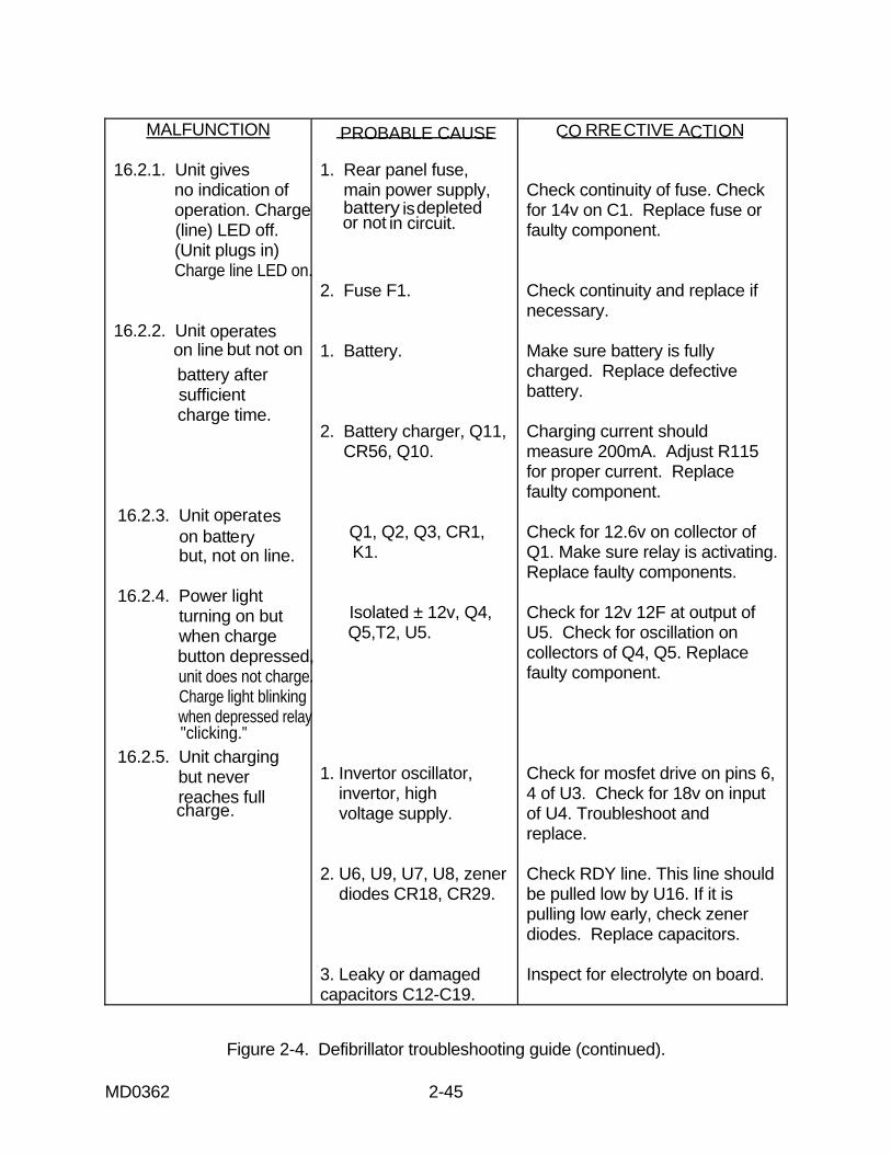
MD0362 2-45
MALFUNCTION 16.2.1. Unit gives no indication of operation. Charge (line) LED off. (Unit plugs in) Charge line LED on. 16.2.2. Unit
operates on line but not on
battery after sufficient charge time. 16.2.3. Unit operates
on battery but, not on line. 16.2.4. Power light turning on but when charge button depressed, unit does not charge. Charge light blinking when depressed relay 16.2.5. Unit charging but never reaches full
PROBABLE CAUSE 1. Rear panel fuse, main power supply, battery
is depleted
or not in circuit.
2. Fuse F1. 1. Battery. 2. Battery charger, Q11, CR56, Q10. Q1, Q2, Q3, CR1, K1. Isolated ± 12v, Q4, Q5,T2, U5. 1. Invertor oscillator, invertor, high voltage supply. 2. U6, U9, U7, U8, zener diodes CR18, CR29. 3. Leaky or damaged capacitors C12-C19.
CO RRECTIVE ACTION
Check continuity of fuse. Check for 14v on C1. Replace fuse or faulty component. Check continuity and replace if necessary. Make sure battery is fully charged. Replace defective battery. Charging current should measure 200mA. Adjust R115 for proper current. Replace faulty component. Check for 12.6v on collector of Q1. Make sure relay is activating. Replace faulty components. Check for 12v 12F at output of U5. Check for oscillation on collectors of Q4, Q5. Replace faulty component. Check for mosfet drive on pins 6, 4 of U3. Check for 18v on input of U4. Troubleshoot and replace. Check RDY line. This line should be pulled low by U16. If it is pulling low early, check zener diodes. Replace capacitors. Inspect for electrolyte on board.
Figure 2-4. Defibrillator troubleshooting guide (continued).
"clicking."
charge.

MD0362 2-46
MALFUNCTION 16.2.6. Unit reaches full charge but does 16.2.7. Unit fires but fails to deliver energy. 16.2.8. Unit delivers incorrect energy. Caution: Voltages present inside the unit are lethal.
PROBABLE CAUSE 1. Paddle set. 2. U15, U14. 1. Paddle set. 2. Delivered energy meter not functioning. 3. CR42, CR43. 1. Delivered energy meter. 2. High voltage regulation. U10, CR31, SW5, U16, CR58, CR32. 3. CR62, U11, U10 and associated components.
CORRECTIVE ACTION Substitute with good component. Repair or replace. Pin 3 should pulse when fire buttons are depressed. Replace faulty component. Substitute with good component. Repair or replace. Fire into external test. Check delivered energy board. Check with ohm meter. Replace faulty components. Check with external tester. Replace faulty component. Put Hv meter on J1 pins 1 and 3. At 360 w/sec, voltage should be 1350v ± 10v. Replace faulty component. Check by substituting with good component. Replace faulty components.
Figure 2-4. Defibrillator troubleshooting guide (continued).
not fire.

MD0362 2-47
MALFUNCTION
16.2.9. Unit fails to fire in sync mode. 16.2.10. Paddle pickup not functioning.
PROBABLE CAUSE 1. No QRS recognition. 2. Monitor not seated properly on defib or connector damaged. 3. Synchronizer circuit not latching relay K3. Check associated components. 1. Paddle set. 2. Missing ±12 or ±6v Q4, Q5, T2, CR82, CR95, CR83, L4, L5, CR86, CR87, or broken pin 3 on rear connector. 3. U45, U46.
CORRECTIVE ACTION Make sure a good QRS is present and rate meter is counting. See monitor troubleshooting guide. Visual inspection. Reseat monitor. Repair or replace damaged connector. Sync relay should latch when button pushed. Troubleshoot sync circuit and repair as required. Substitute with good component. Repair or replace. Check as required for proper supply voltages on U46. Replace faulty component. Inject 2 Mv signal into paddles check output on pin3. Should be 1v. Replace faulty component.
Figure 2-4. Defibrillator troubleshooting guide (concluded).
c. Locate the Cause of the Malfunction (Example 2). SYMPTOM: After charging the defibrillator for 16 hours, the unit still will not work on battery power. However, it works fine while plugged into an ac outlet. (1) Identify malfunction (column 1). Notice that a similar problem exists in section 16.1.14 (Battery not holding charge).

MD0362 2-48
(2) Select a probable cause (column 2). You suspect the problem is caused by an excessive current draw (number 1). (3) Troubleshoot (checking procedure - column 3). You check to see if the unit is putting out a constant 540ma current draw. You refer to the charging circuitry for the monitor in Appendix E (D-23). First you unsolder the anode CR36 from the circuit board and place an ma meter in series between the anode and where it normally sits on the board. Then you plug the unit into a known good ac outlet. You expect to see 540ma on the meter, but you do not. After unplugging the unit and re-soldering the CR36 anode, you refer back to the Probable Cause column to select another probable cause. (4) Select a probable cause (column 1). You suspect the problem is in the CR34 and CR35 circuitry (number 3). (5) Troubleshoot (checking procedure - column 3). Using the volt meter, which is referenced to a ground, you plug the unit into an ac outlet. You read a +12vdc on the cathode of CR35 indicating CR35 is good. Following the circuit, you read the same voltage on the anode of CR34, but 0v at the cathode of CR34. This indicates that CR34 is open. Therefore the problem is CR34. (6) Determine corrective action (column 3). You should replace the faulty CR34 component.
Section II. REMOVE AND REPLACE DEFECTIVE MODULES 2-7. GENERAL Once you have isolated a malfunctioning module, you repair or replace the module. Field repairs are usually limited to replacing worn or damaged parts. Use the following procedures when removing and replacing defective modules of the MRL Porta Pak 90. 2-8. DISASSEMBLE THE MONITOR Follow the procedures for accessing the main circuit board in lesson 1, paragraph 1-3. Use the following procedures to remove the major components. When you have repaired or replaced the defective module, reassemble it by reversing the disassembly procedures. a. Remove the Monitor Main Circuit Board. (1) Disconnect the following five cables: (a) Monitor cable assembly. (b) Battery cable.

MD0362 2-49
(c) CRT high voltage. (d) Load (L) vac input. (e) Deflection cable. (2) Remove the two rear hinge screws that hold the monitor base to the chassis. Separate the monitor form the base. (3) Next, remove the three screws from the under side of the monitor base and the two center screws near the jack at the rear. Carefully lift the board out of the base and place it on the non-metallic surface. b. Remove the Nickel-Cadmium Battery. (1) Remove the two front screws holding the base to the chassis (figure 2-5).
Figure 2-5. Nickel-Cadmium battery replacement. (2) Loosen, but do not remove, the two back screws. (3) Open the monitor and lay it on its side carefully. (4) Disconnect the battery plug from the 590260 board. (5) Remove the single nylon nut and washer retaining the battery enclosure and slide it out of the monitor.

MD0362 2-50
c. Remove the CRT. CAUTION: The high voltage connector cable may have a residual charge and should be discharged to the chassis through a high resistance. (1) Disconnect the high voltage connector (2nd anode) as shown in figure 2-6.
Figure 2-6. Location of CRT high voltage connector. (2) Disconnect the CRT socket (figure 2-7). (3) Remove the two chassis screws holding the grounding wire form (figure 2-7). (4) Remove the CRT assembly.
Figure 2-7. CRT socket disconnect.

MD0362 2-51
CAUTION: Exercise extreme care to avoid breaking the CRT, especially at the neck of the tube. d. Remove the Chart Recorder. (1) Disconnect chart recorder plug (figure 2-8). (2) Remove the four chassis mounting screws holding the chart recorder into the chassis brace. (3) Remove the chart recorder using special care to avoid any damage to the stylus on the center side of the chart recorder assembly (figure 2-9).
Figure 2-8. Chart recorder disconnect.
Figure 2-9. Location of stylus.

MD0362 2-52
2-9. DISASSEMBLE THE DEFIBRILLATOR Follow the procedures for accessing the main circuit board in lesson 1, paragraph 1-3. Use the following procedures to remove the major components. When you have repaired or replaced the defective module, reassemble it by reversing the disassembly procedures. a. Remove the Defibrillator Main Circuit Board. Remove the defibrillator/cardioscope from the MRL Porta Pak 90 case to access the defibrillator main circuit board components. (1) Remove the defibrillator cover plate as a single unit by leaving the three screws on the panel installed and removing the remaining eight screws (figure 1-8). (2) Reach through the paddle set connector opening (at the rear of the defibrillator) and, with your other hand at the front panel edge, carefully lift up the defibrillator cover plates. (3) Disconnect the battery connector (figure 1-9). The battery is secured to the cover plate with one holding screw. CAUTION: Verify that the rear capacitor has been discharged before proceeding. (4) Disconnect the other connectors in the order presented in index in figure 1-9. (5) Slide the defibrillator board forward and lift out the chassis. b. Remove the Paddle Tray. (1) Remove the two screws (orange lead wires) which connect the test load resistor to the paddle tray (figure 2-10). (2) Turn over the defibrillator board and remove the six bottom screws attaching the paddle tray to the board. (3) Remove the paddle tray.

MD0362 2-53
Figure 2-10. Paddle tray test load resistor disconnect. c. Remove the Defibrillator Beeper. NOTE: The beeper connector is located under the paddle tray, so remove the paddle tray before replacing the defibrillator beeper. Refer to paragraph 2-9b. (1) Disconnect the 2-pin connector located under the paddle tray (figure 2-11). (2) Remove the two screws which hold the beeper mounting bracket in place. (3) Place your first and second fingertips under the beeper mounting plate. Use thumb pressure to press down on the beeper spring tabs encircling the edge of the seating hole. The beeper should release easily. d. Remove the Switch Plate. (1) Remove the two mounting screws on board 590235 and carefully lift the board away (figure 2-12). NOTE: The right end of the 590235 board seats into a small slot in the mother board. Be sure to reseat it into the slot when remounting the board. (2) Disconnect the 2-pin plug connecting the battery indicator assembly to the mother board.

MD0362 2-54
Figure 2-11. Defibrillator beeper removal.
Figure 2-12. Switch plate removal.
(3) Turn the board over and remove the four screws holding the switch plate into position. (4) Remove the switch plate. CAUTION : Exercise extreme care when replacing the 590235 board. Do not crush or force the resistors indicated in figure 2-13 out of position.

MD0362 2-55
Figure 2-13. Main circuit board resistors. e. Replace the Switch Lamp. (1) Lift the button cap out of its mount. It is a snap-fit (figure 2-14). (2) Depress the white inner button base so that it is in the ON position. It will expose a grip tab behind the bulb. Using a needle nose pliers, pull up on this tab to release the bulb. (3) When placing the new bulb, be careful to avoid bending the bulb.
Figure 2-14. Switch lamp replacement.

MD0362 2-56
f. Remove the Switch Gear Assembly. Use a .050 hex wrench to loosen the hex screw holding the switch gear on its shaft (figure 2-15). The gear should slide off.
Figure 2-15. Switch gear replacement.
Continue with Exercises

MD0362 2-57
EXERCISES, LESSON 2 INSTRUCTIONS: Answer the following exercises by marking the lettered response that best answers the question or best completes the sentence. After you have answered all of the exercises, turn to "Solutions to Exercises" at the end of the lesson and check your answers. For each exercise answered incorrectly, reread the lesson material referenced with the solution. 1. All synchronized timing signals for the digital monitor section originate with the: a. Capacitor bank. b. Timing generator. c. Monitor power supply. d. Preregulator circuit. 2. You are following the signal in the safety, manual, and automatic dump circuit. The load impedance is higher than 100 ohms. The pulse is extending too long in time, and the bank could be connected to the paddles indefinitely. What is started each time the fire SCR enters conduction to avoid this highly undesirable situation? a. 15msec timer. b. 25msec timer. c. 35msec timer. d. 45msec timer. 3. Which of the following circuits is in the power supply, deflection, or battery charger? a. Comparator. b. Main dc-dc invertor. c. AC/DC convertor. d. Bandpass filter.

MD0362 2-58
4. Which of the following is a circuit in the ground amplifier section? a. Battery charger (NiCad). b. Paddle pick-up filter. c. Preregulator circuit. d. Memory addressing. 5. You want to completely bypass the battery as soon as the defibrillator is plugged into the ac outlet. Where are the circuits located that control this function? a. Main power ON/OFF circuitry. b. Battery charger (NiCad). c. Floating power supply. d. AC power supply. 6. Which of the following is a function of the magnetic deflection circuit? a. Error amplifiers and circuits deliver a push-pull pulse width modulated signal to the power field. b. Applies the full negative bias to grid one of the CRT which cuts off its beam current. c. Runs the monitor and chart recorder totally independent from the battery. d. R231 can control the deflection signal amplitude.

MD0362 2-59
7. Given the following symptom, use the troubleshooting chart (figure 2-4) and refer to the defibrillator schematic in Appendix G to isolate the cause of the malfunction. SYMPTOM: The monitor works perfectly, but the defibrillator charges continuously without ever reaching a full charge. SITUATION: On the oscilloscope, you see that U3 pins 4 and 6 have square wave outputs, 180 degrees out of phase, with alternating 5 and 10 microsecond pulses. With the oscilloscope still referenced to ground, you read the voltage at U4 pin 2. It reads only 10vdc. You followed the circuit (Appendix G) back to CR6 and CR7, and you read 10vdc on the cathode of CR6, but zero v on the cathode CR7. Which item is open and needs to be replaced? a. U4 pin 2. b. U3 pin 4. c. CR6. d. CR7. 8. You have isolated a malfunction to a defective recorder, and you are replacing the recorder. After you disconnect the chart recorder plug, you should: a. Remove the chart recorder. b. Loosen the two rear screws to function as a hinge for easy access to the circuit boards. c. Remove the four chassis mounting screws holding the chart recorder into the chassis brace. d. Remove the two front screws holding the base to the monitor chassis.
Check Your Answers on Next Page

MD0362 2-60
SOLUTIONS TO EXERCISES, LESSON 2 1. b (para 2-2a(4)(a)) 2. c (para 2-2b(3)(a)) 3. b (para 2-3a(2)) 4. b (para 2-3c(3)) 5. d (para 2-4a) 6. d (para 2-3a(3)(a)) 7. d (figure 2-3, section 16.2.5, and Appendix G, section D4-D5) 8. c (para 2-8d(2))
End of Lesson 2

MD0362 A-1
APPENDIX A
Monitor Board Schematic--M 1 of 6

MD0362 A-2
End of Appendix A

MD0362 B-1
APPENDIX B
Monitor Board Schematic--M 2 of 6

MD0362 B-2
End of Appendix B

MD0362 C-1
APPENDIX C
Monitor Board Schematic--M 3 of 6

MD0362 C-2
End of Appendix C

MD0362 D-1
APPENDIX D
Monitor Board Schematic--M 4 of 6

MD0362 D-2
End of Appendix D

MD0362 E-1
APPENDIX E
Monitor Board Schematic--M 5 of 6

MD0362 E-2
End of Appendix E

MD0362 F-1
APPENDIX F
Monitor Board Schematic--M 6 of 6

MD0362 F-2
End of Appendix F
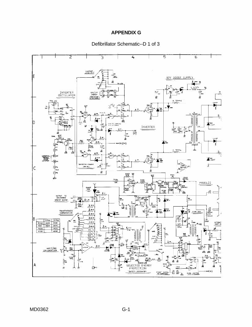
MD0362 G-1
APPENDIX G
Defibrillator Schematic--D 1 of 3

MD0362 G-2
End of Appendix G

MD0362 H-1
APPENDIX H
Defibrillator Schematic--D 2 of 3

MD0362 H-2
End of Appendix H
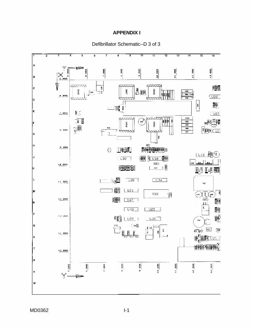
MD0362 I-1
APPENDIX I
Defibrillator Schematic--D 3 of 3

MD0362 I-2
End of Appendix I