mechanics analysis of semiconductor nanotube …
TRANSCRIPT

Adviser:
Professor K. Jimmy Hsia
BY
BRAD ERIC DERICKSON
MECHANICS ANALYSIS OF SEMICONDUCTOR NANOTUBE
FORMATION DRIVEN BY RESIDUAL MISMATCH STRAIN
Urbana, Illinois
THESIS
Submitted in partial fulfillment of the requirements
for the degree of Master of Science in Theoretical and Applied Mechanics
in the Graduate College of the
University of Illinois at Urbana-Champaign, 2010

ii
Abstract
The intent of this thesis is to investigate the formation mechanics of bi-layer
semiconductor nanotubes (SNTs). SNTs are a promising architecture for use in a variety of
applications from quantum structures to building blocks in micro- and nano-eletro-mechanical
systems. Bi-layer SNTs are manufactured using a thin film bending process which relies on the
residual stress in the system due to a lattice mismatch between each layer as the driving force for
formation from a flat plate into a tube. A recent technique utilizing a photolithographic
patterning process has allowed for large scale manufacturability of these tubes. However, when
large scale arrays are constructed using this pattering method, inconsistencies can arise in the
direction along which tubes form. This investigation centers on identifying key parameters
controlling SNT formation in order to identify the source of these inconsistencies. The first
objective pursues determining the energetics associated with tube formation and seeks to identify
which formation states are thermodynamically preferential. The second objective discusses
whether or not the history dependence affects the formation process. It was found that while the
energetics of the process largely dictates the formation characteristics, under special conditions
the history dependence in the process may be the source of the inconsistencies seen.

iii
Acknowledgements
First and foremost, I would like to thank my adviser, Dr. K. Jimmy Hsia, for the
opportunity to work with him and for all of his patience and guidance throughout this project. I
would also like to thank Dr. Xiuling Li and her graduate students for providing experimental
results and for their assistance with this project. Thank you to all of my group members and
fellow students for their help along this journey. Finally, I would like to thank my friends and
family for making this possible through all of their love and support.

iv
Table of Contents
List of Symbols .............................................................................................................. vi
List of Figures ............................................................................................................... vii
List of Tables .................................................................................................................. ix
Chapter 1 Introduction .................................................................................................. 1
1.1 Background and Applications ............................................................................... 1
1.2 System and Formation ........................................................................................... 2
1.3 Experimental Procedure ........................................................................................ 3
1.4 Elasticity ................................................................................................................ 4
1.5 Strain Energy ......................................................................................................... 6
1.6 Stiffness Tensor ..................................................................................................... 7
1.7 Plate Theory .......................................................................................................... 9
1.8 Effects of Thin Films........................................................................................... 10
1.9 Edge Effect .......................................................................................................... 13
1.10 Finite Element Methods of Plates and Shells .................................................. 14
1.11 Figures ............................................................................................................. 17
1.12 Tables............................................................................................................... 24
Chapter 2 Experimental Observation ...................................................................... 25
2.1 System ................................................................................................................. 25
2.2 Experimental Results........................................................................................... 25
2.3 Figures ................................................................................................................. 28
Chapter 3 Research Objectives and Approach ..................................................... 32
3.1 Objectives ............................................................................................................ 32
3.2 Approach ............................................................................................................. 32
3.3 Figures ................................................................................................................. 39
Chapter 4 Results ......................................................................................................... 41
4.1 Anisotropic Etching............................................................................................. 41
4.2 Rolling Energy .................................................................................................... 41
4.3 Etchant Kinetics .................................................................................................. 42
4.4 Edge Effect .......................................................................................................... 43
4.5 Rolling Diameter ................................................................................................. 44
4.6 Figures ................................................................................................................. 46

v
4.7 Tables .................................................................................................................. 56
Chapter 5 Discussion ................................................................................................... 57
5.1 Controlling Mechanisms of Rolling .................................................................... 57
5.2 Etchant Kinetics .................................................................................................. 57
5.3 Edge Effect .......................................................................................................... 58
5.4 Rolling Diameter ................................................................................................. 58
Chapter 6 Conclusions ................................................................................................ 60
References ...................................................................................................................... 61

vi
List of Symbols
M = Bending Moment
b = Body force
ρ = Density
u = Displacement
ν = Poisson’s ratio
ε = Strain
U = Strain Energy
σ = Stress
T = Surface traction
E = Young’s modulus

vii
List of Figures
Figure 1.1: Cross-sectional view of components in bi-layer SNT thin film system ................................................... 17
Figure 1.2: Stress driven formation process of GaAs/InGaAs SNT due to lattice mismatch with AlGaAs sacrificial
layer and GaAs substrate ............................................................................................................................................. 17
Figure 1.3: Types of boundary conditions .................................................................................................................. 18
Figure 1.4: Deformation of a spring subjected to a force ........................................................................................... 18
Figure 1.5: Deformation of an infinitesimal element subjected to uni-axial stress ..................................................... 19
Figure 1.6: Cross-section of a long rectangular strip subjected to pure bending ........................................................ 19
Figure 1.7: Silicon thin film constructed using CVD process .................................................................................... 20
Figure 1.8: Crystallographic alignment of film and substrate during epitaxial growth with substrate thickness taken
to be large compared to the film thickness so that the lattice mismatch is accommodated entirely by the film .......... 20
Figure 1.9: A multilayer epitaxial film composed of alternating layers of film and substrate .................................... 21
Figure 1.10: A thin film substrate depicting a free edge and the traction distribution across the interface between the
film and the substrate ................................................................................................................................................... 21
Figure 1.11: Stresses along the interface of a bi-layer thin film system depicting the solutions of Suhir, Hess, and
Eischen for an aluminum substrate and molybdenum film of equal thickness ............................................................ 22
Figure 1.12: A differential slice from a plate deforming in the absence of shear deformation ................................... 23
Figure 1.13: A differential slice from a plate deforming in the presence of shear deformation ................................. 23
Figure 2.1: SEM images of SNT formation process for a 5 x 10 µm plate ................................................................. 28
Figure 2.2: SEM images of time evolution of SNT formation process for a 10 x 25 µm plate .................................. 28
Figure 2.3: SEM images of time evolution of SNT formation process for a 19 x 50 µm plate .................................. 28
Figure 2.4: STEM image of bi-layer cross-section displaying oxide layer prior to tube formation ........................... 29
Figure 2.5: Array of bi-layer SNTs ............................................................................................................................. 29
Figure 2.6: Array of bi-layers SNTs with inconsistencies in tube formation direction ............................................... 30
Figure 2.7: Wheel pattern used in crystallographic orientation dependence study prior to etching ........................... 30
Figure 2.8: Wheel pattern used in crystallographic orientation dependence study after etching ................................. 31

viii
Figure 3.1: Use of symmetry in finite element modeling and boundary conditions applied ...................................... 39
Figure 3.2: Perturbation applied to FE model to induce rolling along the long side edge .......................................... 39
Figure 3.3: Loading condition for analytical plate model ........................................................................................... 40
Figure 4.1: Notation of dimensions of quarter plate ................................................................................................... 46
Figure 4.2: Results of numerical simulation identifying the transition between long side rolling and short side rolling
for quarter plate geometries with major dimensions 10 x 10-75 µm utilizing a 250 µε mismatch strain .................... 47
Figure 4.3: Results for deformation of short side and long side rolling modes of a 9.5 x 25 µm quarter plate, under a
500 µε mismatch strain, isotropically etched, and with an etched area of 95% ........................................................... 48
Figure 4.4: Results for strain energy as a function of mismatch strain associated with short side and long side rolling
modes of a 9.5 x 25 µm quarter plate, under a 500 µε mismatch strain, isotropically etched, and with an etched area
of 95% ......................................................................................................................................................................... 49
Figure 4.5: Results for strain energy as a function of associated with the different regions of a 9.5 x 25 µm quarter
plate, under a 500 µε mismatch strain, and isotropically etched .................................................................................. 50
Figure 4.6: Results for deformation of a 9.5 x 25 µm quarter plate, under a 500 µε mismatch strain, isotropically
etched and with etched areas of: (a) 20%, (b) 40%, (c) 50%, (d) 60%, (e) 80%, (f) 95% ........................................... 51
Figure 4.7: Results for deformation of plates isotropically etched, under a 1250 µε mismatch strain, with etched
areas of 40%, and with geometries corresponding to: (a) a 4 x 25 µm plate (2 x 12.5 µm simulated) (b) a 19 x 50 µm
plate (9.5 x 25 µm simulated) ...................................................................................................................................... 52
Figure 4.8: Results for a free standing, 20 x 90 µm plate (10 x 45 µm simulated), under a 250 µε mismatch strain . 53
Figure 4.9: Schematic depicting assumed energy-less region along plate edge .......................................................... 53
Figure 4.10: Results for correlation between analytical and numerical models of stresses along the bending direction
of a 10 nm thick plate subjected to a 250 µε mismatch stain ....................................................................................... 54
Figure 4.11: Results for correlation between analytical and numerical models of stresses along the transverse
direction of a 10 nm thick plate subjected to a 250 µε mismatch stain ........................................................................ 54
Figure 4.12: Results for comparison of rolling diameter between analytical models and numerical simulations ...... 55

ix
List of Tables
Table 1.1: Material and system properties used in comparison between methods for determining stress field near a
free edge in a bi-layer system ...................................................................................................................................... 24
Table 4.1: Results from edge effect analysis .............................................................................................................. 56
Table 4.2: Material properties used in rolling diameter calculations .......................................................................... 56

1
Chapter 1 Introduction
1.1 Background and Applications
A recently emerging field in the area of small scale technology has been the nanotube.
This field was perhaps largely initiated by one of the most well known nanotubes, the carbon
nanotube (CNT), which was first introduced by Iijima in 1991 [1].Common techniques for
synthesizing CNT’s include chemical vapor deposition [2], arc discharge [1], and laser ablation
[3]. With their extraordinary strength and unique electrical and physical properties, CNT’s have
spawned extensive research into their application in the fields of nanotechnology, electronics,
and optics amongst others.
In recent years, thin-film bending processes have been utilized to construct nanoscale
devices and sensors [4-5]. This bending mechanism was exploited by Prinz et al in 2000, to form
the first III-V compound semiconductor nanotubes [6]. This new technique for fabricating
nanotubes is very promising due to its capability to self form small objects with ease and
reproducibility. Using this method, SNTs have been formed with diameters as small as 3nm and
10nm from InGaAs/GaAs [6] and SiGe/Si [7] systems respectively. In addition to
semiconductors, this method has also been extended to successfully form micro- and nanotubes
from composites [8-9], metals [10], and polymers [11]. Other objects such as helices [6],
cantilevers, and rings [12] have also been formed. Large scale arrays of InGaAs/GaAs nanotubes
have been created with this technique indicating a large potential for manufacturability [13].
Currently these nanotubes have been exploited to create radial superlattices and nanoreactors
[14], needles for micro injections and ink-jet printing [15], and nanopipelines [16]. In addition to
components for use in MEMS and NEMS, potential applications include micro- and
nanocapacitors [9], micro- and nanocoils and transformers [9, 17], transitors [9], x-ray
waveguiding [18], biology [19] and fluidics [20-21].

2
1.2 System and Formation
In this paper we will focus on the formation mechanism used in the construction of bi-
layer SNTs. In order to create these tubes, two components are necessary. The first component is
a sacrificial layer, between the substrate and the bi-layer, which can be selectively etched away
allowing for complete detachment of the bi-layer. A cross-sectional view showing this system
can be observed in Figure 1.1. The second necessary component is a driving force within the bi-
layer which can be used to drive the rolling of the tube. This driving force can be created either
due to an epitaxial mismatch between the two layers, or be due to an intrinsic surface stress
imbalance due to surface reconstruction [22-23]. In this paper the former case will be of concern
as it serves as the driving force for the tubes studied here.
The rolling mechanism of the system described can be observed in Figure 1.2. This
example system consists of an InGaAs/GaAs bi-layer, along with an AlAs sacrificial layer and a
GaAs substrate. With a larger lattice constant, the InAs is compressively strained after
deposition, as depicted in Figure 1.2(a) and Figure 1.2(b). After the selective etching process is
initiated, the bi-layer begins to detach from the substrate. During this process, the expansion of
the compressively strained InAs layer is resisted by the GaAs. As a consequence, a pair of
opposing forces created between the two layers gives rise to a net moment which acts as the
driving force necessary to roll the tube, as depicted in Figure 1.2(c).
The classical Timoshenko formula for the radius of curvature of a thin bi-metallic strip
can be used to roughly illustrate the dependence of tube diameter on system parameters. This
equation for the diameter is stated as:
� = �3�1 + ��� + �1 + ��� ��� + 1����3�∆���1 + ��� , (1.1)
where t is the total thickness of the bi-layer, m and n are the ratios of the thicknesses and
Young’s moduli of the top and bottom layers respectively, and ∆�, in our case, is the amount of
mismatch strain due to a difference in lattice constants of the two layers [24]. Equation 1.1 can
be simplified further by noting that changes in the values of � close to 1 do not have a significant
effect in the diameter of the strip [24]. If we approximate � = 1, we obtain the following:

3
� = 13�∆�� ! � ", (1.2)
where " and � are thicknesses of the individual top and bottom layers. We can observe that the
tubes diameter depends strongly on the thicknesses of the films and the extent of the mismatch
strain between them. Thus, a means of controlling the tube diameter through tailoring the film
thickness and composition of the bi-layers exists.
1.3 Experimental Procedure
The fabrication process of the tubes begins with the growth of the bi-layer. In the case of
SNTs this can be done using molecular beam epitaxy or chemical vapor deposition methods
[6, 12]. Observing Equation 1.2, by controlling the thickness of these layers during deposition,
the diameter of the tube can be controlled while its length can by the length of the pattern.
Once the strained bi-layer has been deposited, the next step in the process is to expose the
sacrificial layer. This is done in order to allow the etchant solution to access the sacrificial layer
so that the bi-layer can be released from the substrate. Several methods can be used to do this,
such as scratching the surface of the system which creates a cut down to the substrate [25],
selective growth [26], optical lithography [27], and electron beam lithography [28]. The
lithographic patterning methods offer the advantage of greater efficiency, being more
manageable, and greater manufacturability when constructing large patterned arrays.
Consideration of the crystallographic orientation is also taken into consideration during this stage
as the tubes will roll along the crystallographic direction with the least stiffness [22].
After the sacrificial layer has been exposed, an etching process is used to free the bi-layer
from the substrate. An etchant is chosen such that the sacrificial layer is selectively etched,
leaving the bi-layer with little to no disruption. At this stage it should be noted that several of the
processes in the manufacturing of the tubes up until this point can remove material thickness
from the bi-layer. In addition to the selective etching, these processes can include removal of the
photo-resist if a lithographic patterning process was used, as well as the removal of oxide layers
which may form during manufacturing [12].

4
Once the tubes have been formed, several properties of the tubes can be characterized.
The determination of tube diameter as well as imaging of the tubes is carried out through
scanning electron microscopy (SEM). Tube wall thickness measurements can be taken using
scanning transmission election microscopy (STEM), while energy dispersive spectroscopy can
be used to determine the composition of the tube wall [22].
1.4 Elasticity
In 1678, Robert Hooke arguably initiated the field of elasticity when he proposed the
concept of elastic force deformation. Since that time many prominent scientists and
mathematicians have helped developed the mathematical theory of elasticity. This theory
describes the response of elastic bodies subjected to loading.
In order to describe the physics within an elastic body, a set of field equations relating the
stresses, strains, and displacements in the body can be used. A proper set of boundary conditions
can be used to represent the loading of a given body. When the field equations are combined
with the boundary conditions a boundary value problem is formed. This problem can then be
solved to determine the response of the body to the given loading.
In this section we will consider the linearized theory of elasticity. In this theory we
assume the displacement gradients in the body to be small, the stress-strain response of the
material to be linear, and we assume that the material does not reach a stress state which
produces yielding. Under these assumptions the governing field equations for the theory of linear
elasticity can be developed using basic principles of continuum mechanics. Using index notation,
these equations are [29]:
Equilibrium
#$%,$ + &% = '(,) (1.3)
which, in a static body, can be expressed:
#$%,$ + &% = 0. (1.4)

5
Strain-Displacement
�$% = 12 -($,% + (%,$. (1.5)
Stress-Strain
#$% = /$%01�01, (1.6)
which, for an isotropic material, can be written:
#$% = 1 + 23 �$% − 23 �005$% . (1.7)
In order to complete the boundary value problem, a set of appropriate boundary
conditions are needed. Boundary conditions of interest for which a body may be subjected
generally include specifying how the body is supported or loaded. These conditions
mathematically correspond to specifying displacements or tractions along the boundary
respectively. Here, three typical cases exist. The first consists of specifying the displacements
along the entire boundary. The second consists of specifying the tractions along the entire
boundary, while the third is a mixed case consisting of specifying the displacements along one
portion of the boundary and specifying the tractions along another portion of the boundary.
These three cases are illustrated in Figure 1.3. In this paper we will deal with the traction type
boundary condition.
The surface tractions are related to the surface stress and outward normal of the body
through the Cauchy equations. These equations are stated mathematically as [29]:
6$ = #$%�% . (1.8)
In order to obtain a unique solution, we must also check that the displacement field is
single valued. This corresponds to ensuring that two points within the body cannot collapse to a
common point and that voids within the body cannot be created. This compatibility problem
within in a simply connected domain can be expressed in terms of the strains as [29]:
�$%,01 + �01,$% − �$0,%1 − �%1,$0 = 0. (1.9)

6
Equations 1.9 are known as the Saint Venant compatibility equations. Of these 81 equations only
6 are independent. These independent equations are [29]:
�"",�� + ���,"" = 2�"�,"�, ���,!! + �!!,�� = 2��!,�!, �!!,"" + �"",!! = 2�!",!", �"",�! = −��!,"" + �!",�" + �"�,!", ���,!" = −�!",�� + �"�,!� + ��!,"�, �!!,"� = −�"�,!! + ��!,"! + �!",�!. (1.10)
Noting that the strain tensor is the symmetric portion of the displacement gradient and
that it can be shown, using conservation of angular momentum, that the stress tensor is also
symmetric, the system consists of 15 equations in 15 unknowns, 3 displacements, 6 �$%, and 6 #$%.
This is the most general problem; however, simplifications may be made to reduce the
complexity of the system.
1.5 Strain Energy
When an elastic body is subjected to surface tractions and body forces, these loads will
do work on the body. This work will be stored in the body in the form of strain energy. For an
idealized elastic body, when the loading is removed and the body is allowed to return to its un-
deformed configuration, this energy is completely recovered.
A simple illustration of this concept is a Hookean spring subjected to a load 78. Here, the
energy stored in the body is just the work done by the force as it acts through the displacement of
the spring, as depicted in Figure 1.4. The energy stored in this type of body is simply given by:
9 = : 7 ∙ <= = : >? <?@A
B= 12 >?8� = 12 7B?8 . (1.11)
Ideally, this energy stored in the spring is completely released when the force is removed.
Next, we will consider an infinitesimal cubic element which is subjected to a stress σ
normal to its face, as demonstrated in Figure 1.5. We will neglect body forces in this case of
simple uniaxial deformation. Furthermore, we assume that the loading of the element is such that
there are no inertial effects. Applying the same concept as with the previous case, the net energy
7
stored in the body, the strain energy, will be equal to the net work done on the element. This
work is given by:
C = : #< D(" + <("<?" <?"EFGG
B<?� <?! − : # <?"
FGG
B<?� <?!
= : #< D<("<?"EFGG
B<?"<?�<?!
(1.12)
Applying Hooke’s law and the strain displacement equations, the following relation is obtained:
�"" = <("<?" = #""3 . (1.13)
Substituting this relation back into Equation 1.12, the following relation is given:
C = : 3�<�HGGB <?"<?�<?! = 3�""�
2 <?"<?�<?!. (1.14)
More generally the strain energy is given by:
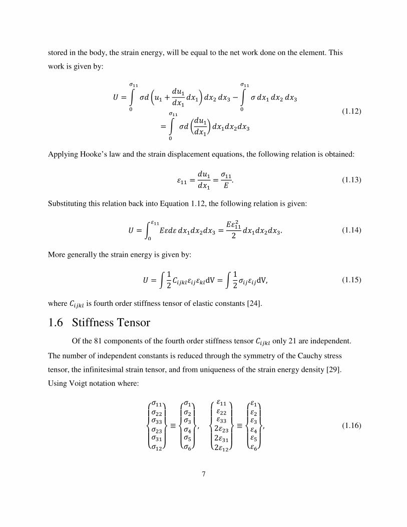
C = : 12 /$%01�$%�01dV = : 12 #$%�$%dV, (1.15)
where /$%01 is fourth order stiffness tensor of elastic constants [24].
1.6 Stiffness Tensor
Of the 81 components of the fourth order stiffness tensor /$%01 only 21 are independent.
The number of independent constants is reduced through the symmetry of the Cauchy stress
tensor, the infinitesimal strain tensor, and from uniqueness of the strain energy density [29].
Using Voigt notation where:
KLMLN
#""#��#!!#�!#!"#"�OLPLQ ≡
KLMLN
#"#�#!#S#T#UOLPLQ,
KLMLN
�""����!!2��!2�!"2�"�OLPLQ ≡
KLMLN
�"���!�S�T�UOLPLQ, (1.16)

8
we can then represent Equation 1.6 in matrix form as:
KLMLN
#"#�#!#S#T#UOLPLQ =
KLMLN
/"" /"� /"! /"S /"T /"U/"� /�� /�! /�S /�T /�U/"! /�! /!! /!S /!T /!U/"S /�S /!S /SS /ST /SU/"T /�T /!T /ST /TT /TU/"U /�U /!U /SU /TU /UUOLPLQ
KLMLN
�"���!�S�T�UOLPLQ. (1.17)
This represents the most general form of the stiffness matrix. For isotropic materials, materials
whose properties are independent in space, there are only two independent constants. For these
types of materials the stiffness tensor matrix representations is expressed as [30]:
KLMLN
#"#�#!#S#T#UOLPLQ =
KLLLMLLLN
/"" /"� /"� 0 0 0/"� /"" /"� 0 0 0/"� /"� /"" 0 0 00 0 0 �/"" − /"��2 0 00 0 0 0 �/"" − /"��2 00 0 0 0 0 �/"" − /"��2 OL
LLPLLLQ
KLMLN
�"���!�S�T�UOLPLQ. (1.18)
The simplest anisotropic materials are those which exhibit cubic symmetry in their crystal
structure. Many group III-V semiconductors have this type of crystal structure. For materials
with cubic symmetry, there are three independent elastic constants. The corresponding stiffness
matrix for these types of materials is given by [30]:
KLMLN
#"#�#!#S#T#UOLPLQ =
KLMLN
/"" /"� /"� 0 0 0/"� /"" /"� 0 0 0/"� /"� /"" 0 0 00 0 0 /SS 0 00 0 0 0 /SS 00 0 0 0 0 /SSOLPLQ
KLMLN
�"���!�S�T�UOLPLQ. (1.19)
The materials considered in this paper are those with cubic crystal structure with stiffness
matrices of that in the form of Equation 1.19. The effective Young’s modulus and Poisson’s ratio
may be calculated with respect to a given direction. All of the calculations considered in this
paper will take place with respect to the V0 0 1W and V0 1 0W crystallographic directions, for which
the effective Young’s modulus given by [31]:
9
3"BB = �/"" + 2/"���/"" − /"���/"" + /"�� , (1.20)
and the effective Poisson’s ratio is given by [31]:
2"BB = /"��/"" + /"��. (1.21)
1.7 Plate Theory
In this section we consider the behavior of thin plates which undergo small deflections.
Here, we define a small deflection as a deflection which is small relative to the thickness of the
plate. For this type of system subject to bending by lateral loads, several assumptions can be
made which lead to an effective approximation of the system behavior. These assumptions are as
follows:
1. There is no deformation in the middle plane of the plate. This plane is commonly referred
to as the neutral plane.
2. Sections which are initially plane and perpendicular to the mid-plane of the plate remain
plane and perpendicular after bending.
3. The normal stresses in the transverse direction of the plate can be neglected.
Under these assumptions the deflection of the plate becomes a function of only the two
in-plane coordinates of the plate. The second assumption neglects the effect of shearing forces on
the deflection of the plate. These results greatly simplify and reduce the governing equations to a
much more manageable system.
As an illustration of this type of problem, we will consider cylindrical bending of a long
rectangular plate, subjected to a transverse load which is constant along the length of the plate.
We consider an elemental strip cut from the plate away from the edges, so that there are no end
effects and the deformation of the plate can be considered cylindrical, as depicted in Figure 1.6.
Under the governing assumptions, and for the given loading, the curvature can be taken equal to
− <�(! <?"�⁄ and the unit elongation of a fiber at a distance z from the mid-surface is then given
by − ?! <�(! <?"�⁄ [32]. Hooke’s law for this problem reduces to:
10
�"" = #""3 − 2#��3
��� = #��3 − 2#""3 = 0, (1.22)
where we observe that #�� = 2#"". We can then rewrite the Equation 1.22 as:
�"" = �1 − 2��#""3 . (1.23)
Inverting Equation 1.23 we find obtain:
#"" = 3�""�1 − 2�� = − 3?!�1 − 2�� <�(!<?"� . (1.24)
Substituting Equation 1.24 into the definition of the bending moment we find:
Y = : #""Z/�
Z/� ?! <?! = − : − 3?!��1 − 2�� <�(!<?"� = − 3ℎ!12�1 − 2�� <�(!<?"�
Z/�Z/� . (1.25)
By rearranging Equation 1.25 we obtain:
<�(!<?"� = −Y 12�1 − 2��3ℎ! . (1.26)
With the bending moment known, the stresses can be determined and thus strains are
known through Equations 1.22. The displacement field is also known through integration of
Equation 1.26. With all of the unknowns uniquely determined, the energy of the system as well
as the curvature of the plate can be determined. This simple example serves as basis for
calculations which will be made later in the paper.
1.8 Effects of Thin Films
1.8.1 Classification
Thin film systems can be categorized based on their physical dimensions and their
intrinsic length scales. The physical dimension of concern in these systems is primarily the
thickness of the film. Intrinsic length scales can include, in a polycrystalline film for example,

11
atomic unit cell size, spacing of crystalline defects, and crystal grain size amongst others. Here
film behavior can change based on how the size of these intrinsic scales compares with the
physical dimensions.
In the case of mechanically thin films, the intrinsic length scales are much smaller than
the film thickness. The thickness of such films is typically on the scale of tens to hundreds of
micrometers. In this category of films, a continuum mechanics approach can usually be used to
adequately describe the mechanical response of the film [31].
In microstructurally thin films, the intrinsic length scales are on the same scale of the film
thickness. The mechanical properties of these films become dependent on grain size, shape,
distribution, and crystallographic texture [31].
Films whose thickness is on the order of a few atomic layers fall into the category of
atomically thin films. In these films the mechanical response is strongly influenced by surface
energy and interatomic potentials rather than macroscopic properties or micromechanisms of
deformation [31].
1.8.2 Epitaxial Films
The two most common methods for transferring material atom by atom to the growth
surface of a film being deposited on a substrate are Physical Vapor Deposition (PVD) and
Chemical Vapor Deposition (CVD). PVD represents a class where physical processes are used to
transfer atoms from a solid or molten source onto a substrate. An example of this technique is a
Molecular Beam Epitaxy, a method where the source material is evaporated at high temperature
in a high vacuum environment, and condenses onto a growth substrate. In CVD a chemical
reaction between a volatile compound and suitable gases is typically used to deposit a
nonvolatile film onto the substrate, as shown in Figure 1.7.
Using either of these methods, for a suitable system and under proper conditions, film
growth can occur epitaxially. This growth refers to the continuation of alignment of
crystallographic atom positions in the single crystal substrate into the single crystal film, as
demonstrated in Figure 1.8. If the film and substrate materials are the same, this arrangement is
known as homoepitaxy, while if they differ the arrangement is known as heteroepitaxy.

12
In the case of heteroepitaxy, the difference in lattice constants between the substrate and
film material gives rise mismatch strain. For a substrate which is substantially thicker than the
film, the film will take on the necessary strain in order to facilitate the atomic alignment.
Denoting the lattice dimension of the stress free film as ]^ and that of the substrate as ]_ , the
mismatch strain is given by:
�` = ]_ − ]^]^ . (1.27)
The energy necessary to facilitate adding material with this strain is offset in very thin films by
the gain associated with the bonding process.
1.8.3 Elastic Strain in Epitaxial Films
The mismatch strain �` gives rise to an elastic strain in the film substrate system. If we
consider the system depicted in Figure 1.9, the elastic mismatch strain must be accommodated by
the film and substrate which leads to the requirement:
�̂ − �_ = �`. (1.28)
The multi-layer system is used here in order to simplify this illustration by removing the effect of
bending. No external loading of the structure is considered. We also assume that we are far from
the perimeter of the system so edge effects need not be considered. Furthermore, we consider the
strain component in the out of page direction, so that the strain state is equi-biaxial. Following a
similar procedure to the example in the previous section, this equi-biaxial state of the thin film
system leads to:
#̂ = 3̂1 − 2̂ �̂ , #_ = 3_1 − 2_ �_. (1.29)
From equilibrium, the net force per unit thickness into the page must be zero, leading to the
condition:
3̂1 − 2̂ �̂ ℎ^ + 3_1 − 2_ �_ℎ_ = 0. (1.30)
Solving Equations 1.29 and 1.30, we find that

13
�̂ = �`ℎ_ � 3_1 − 2_�
ℎ^ D 3̂1 − 2̂ E + ℎ_ � 3_1 − 2_�, �_ = −�`ℎ^ D 3̂1 − 2̂ E
ℎ^ D 3̂1 − 2̂ E + ℎ_ � 3_1 − 2_�. (1.31)
From this result we can observe that in the limit where the substrate is much thicker than
the film, the film accommodates the complete mismatch strain. That is as ℎ^ ℎ_⁄ → 0 then �̂ →�`. We can also observe that the strain in the film is tensile for a tensile mismatch strain.
Similarly when the film is much thicker than the substrate, ℎ^ ℎ_⁄ → 0 then �_ → −�` and the
strain in the substrate is compressive for a tensile mismatch strain. In the systems considered in
this paper, the layers will be of comparable thickness and thus the mismatch strain will be
accommodated by both.
1.9 Edge Effect
In the derivation in the previous section we assumed that we were far from the perimeter
of the system so that edge effects are not considered. The focus of this section is to consider what
happens in the vicinity of the edge.
We start by considering a bi-layer thin film with an epitaxial mismatch, described above,
which induces a bi-axial stress state in the system. The stresses are induced due to the lattice
mismatch. As a thin film layer is deposited onto a substrate, the constraint of the substrate
prevents the film from settling to an unstrained state. If we do not consider the edge effect, a
paradox is presented. Across the film-substrate interface there is zero traction transmitted
everywhere and thus, there can be no interaction between the two layers.
This paradox is resolved when we consider what happens at the edge of the system. Far
from the edge the stress state is bi-axial; however, by noting that there is no externally applied
loading to the system, this stress state cannot exist in equilibrium near the edge. A different stress
state near the edge must exist which permits interaction between the film and substrate. This
interaction is depicted in Figure 1.10. In the most general case there may be a shear stress b�?"�,
normal stress c�?"�, internal extensional force �?"�, internal shear force =�?"�, and internal
bending moment ��?"�.
14
The objective of this problem is to determine the stress state in terms of the film
mismatch stress #`, film thickness ℎ^, and material properties of the system. This is done by
invoking equilibrium in the system everywhere. However, this leads to a coupled set of
governing equations to which no exact solutions exist [31]. Several approaches have been taken
in order to determine the stress state near the edge. An approach using modified beam theory was
considered [33-35], an approach using Airy stress functions [36], as well as an approach using
FEA [37-38].
Plots can be observed in Figure 1.11 comparing the three methods of Suhir [33], Hess
[36], and Eishcen [38]. The system and material properties used for the comparison are given in
Table 1.1 [38]. Good agreement was determined between Hess and Eischen; however, Suhir’s
simplified model did not capture results which were in good agreement. Therefore, we will
confine this discussion to the results of Hess and Eichsen. From these plots we can observe the
stress behavior in the vicinity of the edge, as well as how far inward this stress field propagates
inward. The axial stresses in the system are uniform until approximately thirty percent of the
normalized distance from the edge, where they decay to an asymptote. Approximately thirty
percent away from the edge normal stresses also come into effect, increasing from a value of
zero as the edge is approach for a short distance, then decreasing, reversing sign, and then
increasing negatively with a rapid exponential like behavior toward the edge. The shearing
stresses similarly come into effect around thirty percent of the way from the edge, increasing
rapidly from zero as the edge is approached, and then decaying back to zero at the edge.
This section serves to illustrate the complex stress state which exists near the perimeter of
the system. Furthermore, to illustrate that good agreement with other techniques can be obtained
using finite element modeling.
1.10 Finite Element Methods of Plates and Shells
The finite element method (FEM) is a numerical technique which can be used to obtain
approximate solutions to partial differential equations. Significant development of the method
occurred in the 1950s in order to analyze aircraft structures. With the finite element method the
domain of the body to be analyzed is divided up (or discretized) into many smaller pieces,

15
known as finite elements, which are interconnected at points called nodes. In the case of a
structural analysis, within each element an approximate solution is assumed and the conditions of
complete equilibrium of the structure are derived. The satisfaction of these conditions leads to an
approximate solution for the displacements and stresses throughout the body.
1.10.1 Plates and Shell Elements
Plates and shells are specific forms of three-dimensional solids in which the thickness is
small relative to the other dimensions of the body. These bodies are common structures in
engineering and support transverse loads through bending action. Just as we have beam theory to
characterize the mechanical behavior of beams, we have plate theories to characterize the
behavior of plates and shells. Two common theories are used as formulations in the finite
element method to model the behavior plates and shells and reduce these types of problems to
two dimensions rather than three, significantly reducing computational cost while maintaining
accuracy. The two formulations are the Kirchoff theory for thin plates and shells and the
Reissner-Mindlin theory which is commonly used to model moderately thick plates and shells
1.10.2 Kirchoff
The assumptions used in Kirchoff plate theory are the same as those discussed earlier in
section 1.7, namely:
1. There is no deformation in the middle plane of the plate. This plane is commonly referred
to as the neutral plane.
2. Sections which are initially plane and perpendicular to the mid-plane of the plate, remain
plane and perpendicular after bending
3. The normal stresses in the transverse direction of the plate can be neglected.
These assumptions lead to the governing strain and displacement relations [39]:
(" = −?! d(!d?" , (� = −?! d(!d?� , (! = (!�?", ?��
�"" = −?! d�(!d?"� , ��� = −?! d�(!d?�� , �"� = −?! d�(!d?"d?� , �"! = ��! = 0. (1.32)
16
A plate undergoing this type of deformation can be observed in Figure 1.12. As discussed
in section 1.7, these assumptions are generally acceptable for systems in which the thickness is
thin relative to other dimensions.
1.10.3 Reissner-Mindlin
Contrary to the Kirchoff theory, the Reissner-Mindlin theory accounts for transverse
shear deformation across the thickness. The theory still assumes that stresses normal to the plate
are zero which leads to the following strains displacements [39]:
(" = ?!e�, (� = −?!e", (! = (!�?", ?��
�"" = ?! de�d?" , ��� = −?! de"d?� , �"� = ?! Dde�d?� − de"d?"E, �"! = d(!d?" + e�, ��! = d(!d?� − e".
(1.33)
A plate undergoing this type of deformation can be observed in Figure 1.13. The relaxed
assumptions in this formulation allow for the inclusion of modeling plates which are thicker or
subject to transverse shear.

17
1.11 Figures
Figure 1.1: Cross-sectional view of components in bi-layer SNT thin film system
Figure 1.2: Stress driven formation process of GaAs/InGaAs SNT due to lattice mismatch with AlGaAs sacrificial layer and
GaAs substrate

18
Figure 1.3: Types of boundary conditions
Figure 1.4: Deformation of a spring subjected to a force

19
Figure 1.5: Deformation of an infinitesimal element subjected to uni-axial stress
Figure 1.6: Cross-section of a long rectangular strip subjected to pure bending

20
Figure 1.7: Silicon thin film constructed using CVD process
Figure 1.8: Crystallographic alignment of film and substrate during epitaxial growth with substrate thickness taken to be large
compared to the film thickness so that the lattice mismatch is accommodated entirely by the film

21
Figure 1.9: A multilayer epitaxial film composed of alternating layers of film and substrate
Figure 1.10: A thin film substrate depicting a free edge and the traction distribution across the interface between the film and the
substrate

22
Figure 1.11: Stresses along the interface of a bi-layer thin film system depicting the solutions of Suhir, Hess, and Eischen for an
aluminum substrate and molybdenum film of equal thickness

23
Figure 1.12: A differential slice from a plate deforming in the absence of shear deformation
Figure 1.13: A differential slice from a plate deforming in the presence of shear deformation

24
1.12 Tables
Table 1.1: Material and system properties used in comparison between methods for determining stress field near a free edge in a
bi-layer system
Properties Substrate-Aluminum Film-Molybdenum
Poisson’s Ratio 0.345 0.293 Young’s Modulus 70.38 GPa 325 GPa
Coefficient of Thermal
Expansion 23.6 × 10pU ˚/p" 4.9 × 10pU ˚/p"
Thickness 0.0025 m 0.0025 m Length 0.0254 m 0.0254 m Width 0.001 m 0.001 m
Temperature Change 250 ˚/ 250 ˚/

25
Chapter 2 Experimental Observation
2.1 System
All experimental work carried out in this chapter was conducted by the students of
Professor Xiuling Li of the Department of Electrical Engineering. The formation of SNTs
utilizing the strain-driven mechanism, previously discussed, was carried out by first growing a
planar strained bi-layer structure epitaxially on a �1 0 0� on-axis GaAs growth substrate. The bi-
layer consisted of GaAs and InxGa1-xAs (x =0.2 and x=0.3) with each layer having a thickness of
6 nm. The growth of the bi-layer was carried out using metalorganic chemical vapor deposition.
The sacrificial layer was composed of AlxGa1-xAs (x > 0.6) with thickness which varied from 50
nm to 2 µm. Once deposition was completed, photolithographic patterning was used to define
the undercut mesa for detachment of the bi-layer. The mask used for patterning contained arrays
of squares and rectangles with dimensions of the length and width varying from 1 to 50 µm.
Once patterning was complete and the sacrificial layer was exposed, a timed etch using 1:5
HF:H20 was use to remove the sacrificial layer and thus release the bi-layer from the substrate.
Measurement and imaging were carried out using SEM, STEM, and energy dispersion
microscopy.
2.2 Experimental Results
2.2.1 Tube formation
Tube formation during various stages of the etching process can be observed in Figures
2.1-2.3. It can be observed that as etching begins and proceeds inward, all four sides of the bi-
layer begin rolling along the V0 0 1W and V0 1 0W directions, as depicted in Figure 2.1. Then, as
etching proceeds, a transition occurs and rolling proceeds in one distinct direction, which can be
observed in Figure 2.1, Figure 2.2(c), and Figure 2.3(b), after which the remainder of rolling
continues until the tube is formed, as depicted in Figure 2.1, Figure 2.2(d), and Figure 2.3(c)-
16(d). Eventually, as the entire sacrificial layer is etched away, the tube is placed on the substrate

26
and is held in place by van der Walls forces [40]. By varying the geometry of the initial pattern,
multi turn tubes can be formed as well as double multi-turn tubes, which are shown in Figure
2.3(d).
After deposition of the thin films has occurred, prior to etching, an oxide layer can form
on the exposed upper layer. Figure 2.4 shows a STEM cross-sectional image of the epitaxial
planar structure which has been exposed to air for four months. From Figure 2.4 we can observe
that a portion of the GaAs is consumed through oxidation. Thus, it should be noted that the bi-
layer tube walls are not the same thickness as the initial deposition thicknesses.
2.2.2 Inconsistencies in rolling direction
Large scale arrays of tubes have been formed thanks to the flexibility of the lithographic
patterning process. These arrays can be observed in Figure 2.5. For many applications it is
desirable to have consistency in these arrays. However, for certain geometry patterns, large
inconsistencies may occur. These inconsistencies can be observed in Figure 2.6. The
inconsistencies come in the form of non-uniform rolling direction of the tubes. As opposed to
Figure 2.5 where the tubes consistently roll in one direction, in Figure 2.6 the tubes tend to roll in
multiple directions. In Figure 2.6, approximately eighty-five percent of the tubes rolled up along
the short side of the initial rectangular pattern yielding shorter tubes with more rolls.
Approximately ten percent of the tubes rolled up along the long side of the pattern which yielded
longer tubes with thinner walls. While in approximately five percent of the tubes there was no
distinct rolling direction, different regions of the pattern rolled in different directions and no
actual tube was ultimately formed. These inconsistencies not only lead to non uniform arrays but
also non-form tube properties due to inconsistencies in length and wall thickness.
2.2.3 Rolling diameter
For mainly applications it is also desirable to obtain a precisely tailored tube diameter in
order to obtain optimal mechanical and electrical characteristics. Tube diameter measurements
were taken using SEM for a tube formed bilayer of In0.2Ga0.8As and GaAs with thicknesses of
5.8 and 5.2 nm respectively. Equation 1.1 was used to predict the diameter of the tube. Young’s
modulii E(In0.2Ga0.8As) =75.1 GPa and E(GaAs)=85.6 GPa were used along with a mismatch
strain of 0.01434 [22]. The predicted tube diameter of 1024 nm was not consistent with the

27
measured diameter of 884 nm. Other experiments showed similar results with the actual diameter
being consistently lower than the theoretical prediction when using this model.
2.2.4 Crystallographic orientation dependence
Due to anisotropic stiffness in cubic crystals along different crystallographic directions,
experiments were conducted to observe SNT formation when patterned along different
directions. A wheel using eight anchored rectangular strip pads oriented along V1 0 0W and V1 1 0W directions was formed using the patterning process previously described. The substrate
was (0 0 1) GaAs. This wheel can be observed in Figure 2.7. The dimensions of each strap were
20 µm in length, 15 µm in width, with 5 µm anchors. Tube formation results after the bi-layer is
released from the substrate can be observed in Figure 2.8. It can be seen that despite different
crystallographic orientations, rolling persisted along the V1 0 0W direction for all pads. The
stiffness of GaAs along the V1 0 0W direction is 85.3 GPa, while along the V1 1 0W the stiffness is
121.3 GPa [55-56], indicating that rolling took place along the direction with the least amount of
stiffness.

28
2.3 Figures
Figure 2.1: SEM images of SNT formation process for a 5 x 10 µm plate
Figure 2.2: SEM images of time evolution of SNT formation process for a 10 x 25 µm plate
Figure 2.3: SEM images of time evolution of SNT formation process for a 19 x 50 µm plate

29
Figure 2.4: STEM image of bi-layer cross-section displaying oxide layer prior to tube formation
Figure 2.5: Array of bi-layer SNTs

30
Figure 2.6: Array of bi-layers SNTs with inconsistencies in tube formation direction
Figure 2.7: Wheel pattern used in crystallographic orientation dependence study prior to etching

31
Figure 2.8: Wheel pattern used in crystallographic orientation dependence study after etching

32
Chapter 3 Research Objectives and Approach
3.1 Objectives
As was previously discussed, for the various applications of strain driven self rolling
nanotubes, uniformity in the tube fabrication process is necessary to achieve the desired
mechanical properties and functionality of the tubes. Based on experimental results presented
earlier, we have seen that consistent manufacturing characteristics of these tubes can sometimes
be difficult to obtain. Thus, it is critical to study and explain the rolling mechanisms, as well as
the parameters controlling the rolling process of these tubes, so that uniform, large scale,
manufacturing of the tubes may be consistently obtained.
The objectives of this paper are to study the system outlined in section three and include
the following:
1. Understand parameters controlling the rolling process by studying kinetics of the etching
process.
2. Understand parameters controlling the rolling process by studying the energetics
associated with tube formation .
3. Determine whether tube formation is kinetically controlled, energetically controlled, or
both.
4. Present an updated model to more accurately predict the rolling diameter of the tubes.
3.2 Approach
For each of the objectives, the following approach taken was as follows

33
1. An F.E. model will be used to determine the effect that anisotropy in the etching process
has on the rolling behavior. This model will also be used to determine how the
deformation of the tube during etching can lead to anisotropy in the etching process.
2. An F.E. model will be used to determine the energy associated with each of the rolling
directions, the long side rolling direction and the short side rolling direction. This model
will also be used to study the evolution of the energy in the system as etching proceeds.
The impact in energy on the system due to the edge effect near the periphery of the tube
will also be determined in order to understand this effect’s contribution to the rolling
behavior in the system. This will be done through the comparison of an analytical model
which does not account for the edge effect and a finite element model which does
account for the edge effect.
3. Results from 1 and 2 will be compared with experimental results to determine the
mechanism controlling the formation process.
4. The model previously used to predict the rolling diameter, Equation 1.1, will be replaced
with an updated model which account for out of plane effects. These results will be
compared with experimental results.
3.2.1 F.E. Model
Finite element (FEM) modeling was used to simulate the rolling behavior of the
nanotubes using ABAQUS. The bilayer of InxGa1-xAs and GaAs was simulated using reduced
integration, eight-noded, S8R quadratic thick-shell elements. These elements utilize a Mindlin
type shell formulation previously discussed. Though the geometries simulated were very thin and
in general, accounting for transverse shear would not be necessary for accuracy, these elements
were used in this application due to the non-uniform effects at the perimeter of the plate caused
by the edge effect. These elements permit variation in properties through the thickness so that the
bi-layer may be simulated with one element in the thickness direction. The bi-layer was
simulated by defining two sections across the thickness of the element with the specified
thickness and properties of each of the bi-layers. Simpson integration was used with 5 integration
points through the thickness of each section, ten in total through the thickness of the element.
The reduced integration formulation was used because it generally provides more accurate
results and while reducing running time [43].

34
The materials are assumed to be elastic. Parameters for the elastic properties of each
material used in the simulation are taken from literature [44-45]. To simulate the epitaxial
mismatch strain between the layers, different in-plane coefficients of thermal expansion were
assigned to the InxGa1-xAs and GaAs sections (in the simulations, the thermal expansion
coefficient of GaAs is assigned to be zero). A mismatch strain of prescribed magnitude can then
be induced by introducing a temperature change. To reduce computational time, symmetry
condition was invoked, and only one quarter of the plate was modeled by applying the
appropriate boundary conditions which are shown in Figure 3.1. Due to the large amount of
deformation in the rolling process, non-linear geometry was specified in the analysis to account
for geometric non-linearity.
In all simulations, the temperature change is ramped up until the prescribed mismatch
strain level is reached. For a given geometry (length, width, and the dimensions of the etched
portion), only one rolling mode is achieved as the temperature change increases. However, to
understand the controlling mechanisms of rolling process, the total strain energy of different
rolling behaviors (long side, short side) needs to be evaluated. To simulate different rolling
behavior, a perturbation was applied to the model. During the initial stage of the simulation, one
of the edges would be clamped down to promote rolling of the other edge. A small temperature
change was applied, and the edge was then released for the remainder of the simulation. For
example, to induce rolling along the long side edge, the short side edge was initially clamped
during the perturbation and subsequently released. A schematic of this perturbation can be
observed in Figure 3.2. It was observed that once one side (long or short or mixed) started to roll,
it would continue to roll even after the artificial clamping of the other side is released, regardless
whether it has a higher total strain energy. The resulting model allowed for energy calculations to
be made at a fixed point in the etching process. Various points during the etching process could
be simulated by changing the dimensions.
3.2.2 Analytical Model
A free-standing bi-layer plate under a planar epitaxial mismatch is considered. The
section of an infinite plate considered is subject to the given conditions in Figure 3.3. The plate
under consideration may be a cubic material oriented along the V0 0 1W or V0 1 0W directions so

35
that the effective Young’s modulus and Poisson’s ratio used through Equations 1.20 and 1.21.
Under the assumptions of thin shell plate theory, the equations governing the system are then the
following:
Constitutive:
�""" = − Y"?�r"3" + s"t"3" − 2"�!!" , (3.1)
�""� = − Y�?�r�3� + s�t�3� − 2��!!� , (3.2)
�!!" = a = constant, (3.3)
�!!� = b = constant, (3.4)
#!!" = 3"1 + 2" �!!" + 2"3"�1 + 2"��1 − 2"� ��""" + �!!" �, (3.5)
#!!� = 3�1 + 2� �!!� + 2�3��1 + 2���1 − 2�� ��""� + �!!� �, (3.6)
#""" = 3"1 + 2" �""" + 2"3"�1 + 2"��1 − 2"� ��""" + �!!" �, (3.7)
#""� = 3�1 + 2� �""� + 2�3��1 + 2���1 − 2�� ��""� + �!!� �. (3.8)
Equilibrium:
s" = −s�, (3.9)
Y" + Y� = Z��s" − s��, (3.10)
: #!!" <t" = : #!!� <t�. (3.11)
Compatibility:
�!!" D?� = − "2 E = �!!� D?� = �2 E + ∆�, (3.12)

36
�""" D?� = − "2 E = �""� D?� = �2 E + ∆�, (3.13)
where ∆� is the epitaxial mismatch strain created by the difference in lattice coefficients of the
two materials. We take the plates to have the same width w . We also assume the radii of curvature of the two plates are equal, which leads to: '" = '�, (3.14)
Equation 3.14 can also be expressed as the relation:
Y"3"r" = Y�3�r�. (3.15)
By noting r = 1 12 � !⁄ and rearranging Equation 3.15, the following relation is obtained:
Y� = 3� �!3" "! Y". (3.16)
Using the equilibrium conditions, Equations 3.9 and 3.10, along with Equation 3.16, it can also
be shown:
Y" = 3" "!3" "! + 3� �!� " + ��2 s", (3.17)
Y� = 3� �!3" "! + 3� �!� " + ��2 s". (3.18)
Substituting Equations 3.3 and 3.4 into Equation 3.12, the compatibility condition becomes:
] = & + ∆�. (3.19)
Substituting Equations 3.1 and 3.2 into Equation 3.13, the remaining compatibility condition
becomes:
Y" "2r"3" + s"t"3" − 2"] = − Y� �2r�3� + s�t�3� − 2�& + ∆�. (3.20)
Substituting Equation 3.9, 3.17, and 3.18 into Equation 3.20 and simplifying the following
relation is obtained:

37
s"� �3"� "S + 3�� �S + 43"3� "! � + 43"3� " �! + 63"3� "� ��3"�3� "S � + 3"3�� " �S � − 2"] + 2�& = ∆�. (3.21)
Substituting the constitutive relations for the stresses and strains, Equations 3.1-3.6, into the
equilibrium condition in the transverse direction, Equation 3.11, the following is obtained:
: : ]3"1 + 2" + 2"3"1 − 2"� D− Y"?�r"3" + s"t"3" − 2"] + ]E <?"<?�� ��
p� ��
�G ��
p�G ��=
(3.22)
: : &3�1 + 2� + 2�3�1 − 2�� D− Y�?�r�3� + s�t�3� − 2�& + &E <?"<?�,� ��
p� ��
�� ��
p�� ��
integrating and simplifying it is found:
s"� � 2"1 − 2"� − 2�1 − 2��� + ]3" " + &3� � = 0. (3.23)
By noting the materials under consideration are similar, taking the approximation 2" = 2�, and
solving Equations 3.19, 3.21 and 3.23 for the three unknowns s", ], and & it can be shown:
s" = �∆��1 + 2� � 3"�3� "S � + 3"3�� " �S3"� "S + 3�� �S + 43"3� "! � + 43"3� " �! + 63"3� "� ���, (3.24)
] = 3� �∆�3" " + 3� �, (3.25)
& = − 3" "∆�3" " + 3� �. (3.26)
Having determined s", ], and & the complete stress and strains fields are known through
Equations 3.1-3.8. This allows for a determination of the strain energy of the system through
Equation 1.15. This leads to:
C = : : : 12 �#""" �""" + #!!" �!!" �<?"<?� <?!� ��
� ��
�G ��
�G ��
� ��
� ��+ (3.27)

38
: : : 12 �#""� �""� + #!!� �!!� �<?"<?� <?!� ��
� ��
�� ��
�� ��
� ��
� ��.
Substituting Equations 3.1-3.8 and carrying out the integration, it is found:
C = �92 3"1 − 2"� � Y"� "!12r"�3"� + s"� "t"�3"� + ]� "�1 − 2"��� +
(3.28) �92 3�1 − 2�� � Y�� �!12r��3�� + s�� �t��3�� + &� ��1 − 2����,
where all parameters are known. Furthermore, noting ' = 3r Y⁄ , the diameter of the tube,
� = 2', can be determine using Equations 3.17 and 3.24, which leads to the following relation:
� = 3"� "S + 3�� �S + 43"3� "! � + 43"3� " �! + 63"3� "� ��3� " + ��3"3� " �∆��1 + 2� . (3.29)
It can easily be verified that the equilibrium equations, compatibility, and, by
construction, the boundary conditions, are all satisfied and thus we have a unique solution. We
also note this model follows thin-shell plate theory while the finite element model uses a Mindlin
formulation. Far from the edge we expect both models to follow thin shell behavior due to the
dimensions of the plate; however, due to non-uniform effects near the perimeter of the plate due
to the edge effect, a Mindlin theory was used in the finite element model in order to account for
shear effects in this region. Since there is no edge accounted for in the analytical model, it was
not necessary to account for the edge effect, and thus a thin shell formulation was suitable. It is
expected, and will later be shown, that far from the edge of the plate, both models will converge
to the same results.
For both models we also implicitly take a continuum mechanics approach. Though, the
dimensions of the system fall into the class of a microstructurally thin film system, due to the
growth process used, the system is highly ordered and defect free allowing for this approach to
be used.

39
3.3 Figures
Figure 3.1: Use of symmetry in finite element modeling and boundary conditions applied
Figure 3.2: Perturbation applied to FE model to induce rolling along the long side edge

40
Figure 3.3: Loading condition for analytical plate model

41
Chapter 4 Results
4.1 Anisotropic Etching
Simulations were carried out to study the effect that anisotropy in the etching process
may have on the formation direction of the tubes. Transitions between long-side rolling and
short-side rolling were identified. These transitions are plotted for the amount of anisotropy in
etching as a function of the ratio of major dimensions of the plate. Notation of these dimensions
can be observed in Figure 4.1 for the quadrant of the plate simulated. The notation for the
amount of anisotropy is given by:
∆&∆] = &B − &"]B − ]". (4.1)
A value of one for this ratio represents the case of isotropic etching, the larger the deviation from
a value of one, the greater the amount of anisotropy in the etching. The ratio ]" ]B⁄ was held
constant for each series of simulations and various values of this ratio were simulated. Results
from these simulations are demonstrated in Figure 4.2. The lines in Figure 4.2 represent the
transition between long side rolling and short side rolling. For points above each line, short-side
rolling occurred, for points below each line, long-side rolling occurred.
4.2 Rolling Energy
Further simulations were carried out to observe the energy in the system as a function of
mismatch strain for the cases of long-side rolling, and short-side rolling. A perturbation,
previously discussed, was applied to the model to induce each rolling mode. The amount
mismatch strain induced in the perturbation was below that of the critical bifurcation strain
which was determined to be approximately 2.5 µε. Deformation plots of the rolling modes can be
observed in Figure 4.3. The results for strain energy plotted as a function of mismatch strain can
be observed in Figure 4.4. For this case, the plate naturally rolled toward the long side direction,

42
shown in Figure 4.3(a), while a perturbation was required to induce the short side rolling case,
shown in Figure 4.3(b). In Figure 4.4, it can be observed that long side rolling is the lower
energy rolling direction. This was always found to be the case for isotropic etching once a
distinct rolling direction occurred.
Additional simulations were carried out in order to study the evolution in energy of the
system as etching proceeded. Simulations were performed at various stages in the etching
process, starting from 10% of the total area etched up to 95% of the total area etched. The case of
isotropic etching was simulated. The energy in the etched region of the plate, the unetched region
of the plate, and the total energy in the system are plotted in Figure 4.5. It can be observed that as
etching proceeds during the tube formation process, the total energy of the system decreases.
Plots of the deformation at distinct stages in the etching process are demonstrated in Figure 4.6.
It can be observed that during the initial stages of etching, mixed mode rolling case occurs before
transitioning to a distinct rolling direction, which is consistent with experimental observation.
Once approximately 50% of the total area is etched, shown in Figure 4.6(c), a transition from
mixed mode rolling, to long side rolling occurs. In all simulations performed for isotropic
etching, regardless of geometry, the transition from mixed rolling was always to the long side
rolling direction. A transition to the short side direction never occurred. During experiments,
transitions were primarily to the long side direction, as depicted in Figures 2.1-2.2, however, for
certain geometries it was possible for transition to the short side to occur, as shown in Figure 2.3.
These geometries for which a transition to short side rolling was experimentally observed were
simulated and the transition was always to the long side rolling direction.
4.3 Etchant Kinetics
As previously discussed, based on energetics alone, for isotropic etching, rolling along
the long side always becomes more energetically favorable based on simulation results.
However, experimentally tube formation along the short side is also possible. In order to
examine other possibilities for this explanation, the deformation characteristics during tube
formation were studied in order to determine whether the transport of etchant was affected by the
geometry of plate used during tube formation. Two geometries were specifically studied to

43
compare with experimental results. A 19 x 50 µm plate was simulated as well as a 4 x 25 µm
plate which experimentally exhibited formation along the short side and long side respectively.
Deformation characteristics were studied during early stages of the etching process before a
distinct rolling direction was obtained. Results for these simulations can be observed in Figure
4.7. It can be observe that the deformation patterns for the two geometries are distinctly different
at the corner. In Figure 4.7(a), the 4 x 25 µm plate, the entire corner of the plate rolls ups. On the
other hand, in Figure 4.7 (b), the 19 x50 µm plate, the corner rolls up along the short side of the
plate while the portion of the corner along the long side of the plate remains flat.
4.4 Edge Effect
By comparing the energy calculated from the analytical model, which does not account
for the edge effect, to the energy of the finite element model, which accounts for the edge effect,
the impact of the edge effect on the energetics of the system could be determined. For these
calculations a quadrant of a free standing plate was simulated. Results from a simulation can be
observed in Figure 4.8. It can be seen that along the direction where the rolling occurs, the short
side direction in Figure 4.8, there is no apparent edge effect due to the relaxation of the plate in
this direction. Energy calculations from the analytical model, Equation 3.28, were compared to
those of the finite element model. It was assumed that the reduction in energy due to the edge
effect was confined to a distinct energy-less region along the edge. This region can be observed
in Figure 4.9. The width of this region was determined through the difference between the
energy of the analytical and numerical models. Results from the series of simulations performed
can be observed in Table 4.1. It can be observed that as the plate becomes wider, the reduction in
energy in the system due to the edge effect becomes relatively less prominent. While for
geometries which are narrower, the edge effect has a more significant impact on the energy in
the system. By observing column six of Table 4.1, we can notice that regardless of the
dimensions of the system, the width of the approximated energy-less region does not change.
In order to correlate results from the analytical model and the finite element model, the
stresses were compared. Stresses from the finite element model were taken at the center of the
plate so that non-uniformities in the stress field due to the edge effect would not be present.

44
Results for stresses are plotted through the thickness of the plate in the bending direction and the
transverse direction. These results can be observed in Figures 4.10 and 4.11 respectively.
4.5 Rolling Diameter
Calculations were made with Equation 3.29 to determine if the rolling diameter of the
tube could accurately be determined given the system parameters. These results were compared
to experimental measurements. Material properties used in all calculations are listed in Table 4.2
[46]. The effective Young’s modulus and Poisson’s ratio along the V1 0 0W direction were
calculated using Equations 1.20 and 1.21 respectively. In Equation 3.29 it was assumed that the
Poisson’s ratio of the two layers was the same, to account for this, the average Poisson’s ratio of
the two layers was used in all calculations. The mismatch strains were calculated using Equation
1.27.
Comparing calculations to those listed for the system in [22], for a mismatch strain of ε =
0.01433 and thicknesses of the In0.2Ga0.8As and GaAs layers of 5.8nm and 5.2nm respectively, a
diameter of 779nm is calculated using Equation 3.29, while a diameter of 1024 nm is predicted
by using Equation 1.1. The experimentally measured diameter of this tube was found to be 884
nm.
A comparison was also performed for the system in [13]. For thicknesses of the
In0.3Ga0.7As and GaAs layers of 6 nm each and a mismatch strain of 0.0215, a rolling diameter of
565 nm is calculated using Equation 3.29, while a diameter of 745 nm is predicted using
Equation 1.1. These results are compared with the experimentally measured values of 590 nm.
It was observed that while Equation 1.1 provides a plane stress prediction for rolling
diameter and Equation 3.29 provides a plane strain model, experimental results fell in between
both models. To investigate the out of plane effect, diameters were taken from numerical
simulations and compared with Equation 1.1 and Equation 3.29 as a function of aspect ratio of
the plate width to plate thickness. All results were normalized by the Equation 1.1 and are
depicted in Figure 4.12.

45
As previously discussed the formation of oxide layers during production as well as
deviation of the patterns from the primary crystallographic direction during deposition will affect
experimental results and thus perfect agreement should not be expected. The uniformity in tube
diameter along the length of a given tube as well as between tubes has been seen to have as high
as a 9% standard deviation.

46
4.6 Figures
Figure 4.1: Notation of dimensions of quarter plate

47
Figure 4.2: Results of numerical simulation identifying the transition between long side rolling and short side rolling for quarter
plate geometries with major dimensions 10 x 10-75 µm utilizing a 250 µε mismatch strain

48
Figure 4.3: Results for deformation of short side and long side rolling modes of a 9.5 x 25 µm quarter plate, under a 500 µε
mismatch strain, isotropically etched, and with an etched area of 95%

49
Figure 4.4: Results for strain energy as a function of mismatch strain associated with short side and long side rolling modes of a
9.5 x 25 µm quarter plate, under a 500 µε mismatch strain, isotropically etched, and with an etched area of 95%

50
Figure 4.5: Results for strain energy as a function of associated with the different regions of a 9.5 x 25 µm quarter plate, under a
500 µε mismatch strain, and isotropically etched

51
Figure 4.6: Results for deformation of a 9.5 x 25 µm quarter plate, under a 500 µε mismatch strain, isotropically etched and with
etched areas of: (a) 20%, (b) 40%, (c) 50%, (d) 60%, (e) 80%, (f) 95%

52
Figure 4.7: Results for deformation of plates isotropically etched, under a 1250 µε mismatch strain, with etched areas of 40%,
and with geometries corresponding to: (a) a 4 x 25 µm plate (2 x 12.5 µm simulated) (b) a 19 x 50 µm plate (9.5 x 25 µm
simulated)

53
Figure 4.8: Results for a free standing, 20 x 90 µm plate (10 x 45 µm simulated), under a 250 µε mismatch strain
Figure 4.9: Schematic depicting assumed energy-less region along plate edge

54
Figure 4.10: Results for correlation between analytical and numerical models of stresses along the bending direction of a 10 nm
thick plate subjected to a 250 µε mismatch stain
Figure 4.11: Results for correlation between analytical and numerical models of stresses along the transverse direction of a 10
nm thick plate subjected to a 250 µε mismatch stain

55
Figure 4.12: Results for comparison of rolling diameter between analytical models and numerical simulations
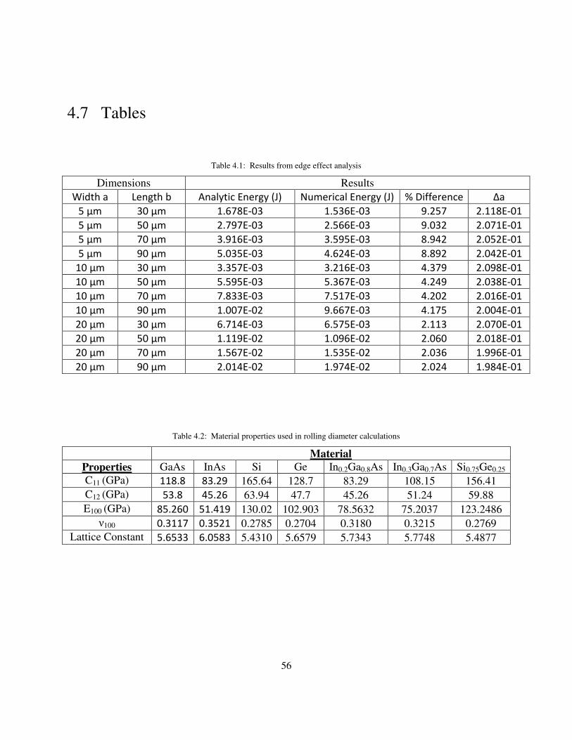
56
4.7 Tables
Table 4.1: Results from edge effect analysis
Dimensions Results
Width a Length b Analytic Energy (J) Numerical Energy (J) % Difference ∆a
5 μm 30 μm 1.678E-03 1.536E-03 9.257 2.118E-01
5 μm 50 μm 2.797E-03 2.566E-03 9.032 2.071E-01
5 μm 70 μm 3.916E-03 3.595E-03 8.942 2.052E-01
5 μm 90 μm 5.035E-03 4.624E-03 8.892 2.042E-01
10 μm 30 μm 3.357E-03 3.216E-03 4.379 2.098E-01
10 μm 50 μm 5.595E-03 5.367E-03 4.249 2.038E-01
10 μm 70 μm 7.833E-03 7.517E-03 4.202 2.016E-01
10 μm 90 μm 1.007E-02 9.667E-03 4.175 2.004E-01
20 μm 30 μm 6.714E-03 6.575E-03 2.113 2.070E-01
20 μm 50 μm 1.119E-02 1.096E-02 2.060 2.018E-01
20 μm 70 μm 1.567E-02 1.535E-02 2.036 1.996E-01
20 μm 90 μm 2.014E-02 1.974E-02 2.024 1.984E-01
Table 4.2: Material properties used in rolling diameter calculations
Material
Properties GaAs InAs Si Ge In0.2Ga0.8As In0.3Ga0.7As Si0.75Ge0.25
C11 (GPa) 118.8 83.29 165.64 128.7 83.29 108.15 156.41
C12 (GPa) 53.8 45.26 63.94 47.7 45.26 51.24 59.88
E100 (GPa) 85.260 51.419 130.02 102.903 78.5632 75.2037 123.2486
ν100 0.3117 0.3521 0.2785 0.2704 0.3180 0.3215 0.2769
Lattice Constant 5.6533 6.0583 5.4310 5.6579 5.7343 5.7748 5.4877

57
Chapter 5 Discussion
5.1 Controlling Mechanisms of Rolling
Increasing a1/a0 can be thought of as the increase in time during etching. As etching
proceeds, for a given geometry, during initial stages a large amount of anisotropy in the etching
process is required for a transition to occur between long side and short side rolling. However, as
etching continues, the sensitivity to anisotropy in the etching process increases and much smaller
changes in etching can cause a transition. Finally, at the later stages in the etching process any
anisotropy makes it thermodynamically favorable for a transition to occur. Nonetheless, at this
stage, a distinct rolling directions has usually occurred making it difficult or impossible for a
tube to roll up, e.g. the tube already has completed a full roll in one direction.
In the case of isotropic etching, based on simulations, it was found that a transition to the
long side rolling direction was always thermodynamically favorable compared with rolling along
the short side, as depicted in Figure 4.4. Experimental results show that most often rolling along
the long side occurs however, rolling along the short side is sometimes observed.
5.2 Etchant Kinetics
Based on the results described in section 5.1.1, if isotropic etching occurs, it is always
expected that the tubes should roll up along the long side. However, contrary to these results,
experimentally it is possible for tubes to form along both directions. One possible explanation for
this result is that in practice, the etching process may not always take place isotropically.
Experimentally it was observed that 19 x 50 µm plates rolls up along the short side while 4 x 25
µm plates roll up along the long side. During simulations, both of these geometries roll up along
the long side in the case of isotropic etching. However, when these geometries were simulated at
earlier stages in the etching process, as depicted in Figure 4.7, it was seen that the corner of the
19 x 50 µm plate, Figure 4.7(b), rolls up along the short side while staying flat along the long

58
side. This deformation behavior would tend to promote access of etchant to the sacrificial layer
on the short side while inhibiting it on the long side of the plate. This result would clearly
promote anisotropy in the etching process, leading to the possibility of rolling along the short
side of the plate based on earlier results. On the other hand, the corner of the 4 x 25 µm plate,
shown in Figure 4.7(a), tends to roll up uniformly in both directions. This uniformity would lead
to isotropic etching and thus rolling up along the long side of the plate. Both of these results are
consistent with the experimental observations which were observed for these geometries.
5.3 Edge Effect
From the results in Table 4.1, it is seen that for plates which are narrower, the energy
reduction in the system to the edge effect becomes more prominent. Noting that the width of the
energy-less region which was assumed is relatively constant regardless of the plate dimensions,
rolling along the short side would reduce more energy in the system than rolling along the long
side with respect to the edge effect. Although, overall it may still be more energetically favorable
to roll along the long side, for more narrow geometries the amount of favorability would not be
as significant. This result may cause inconsistencies or irregularities in the formation process to
have a greater chance to promote short side rolling in more slender geometries. This result is
consistent with the rolling directions which were observed with the 4 x 25 µm and the 19 x 50
µm plates.
5.4 Rolling Diameter
In literature previous calculations to determine rolling diameter were carried out using
Equation 1.1. However, Equation 1.1 is modeled under the assumption of plane stress for thin
strips. Using this equation the values of the diameter were consistently larger than measured
values by approximately 14-16%. Nevertheless, the model presented here accounts for out of
plane thickness which is not thin compared with the other dimensions of the plate and should
thus more accurately model the rolling diameter of the tubes. The model presented here however,
tends to consistently predict rolling diameters smaller than measure value by 4-12%. Based on
the results in Figure 4.12, it is observed that the out of plane dependence becomes important
once the width to thickness ratio becomes larger than 20. At values below this ratio, results

59
converge to Equation 1.1. At aspect ratios approaching 2000 and larger, results converge to
Equation 3.29. In between these ratios neither model provides an accurate description of the
rolling diameter. It can also be observed that Equation 1.1 and Equation 3.29 do not provide
bounding limits. Rather, it is proposed that for smaller aspect ratios there is no edge effect due to
the plane stress state and results are consistent with Equation 1.1. As the aspect ratios tend to
increase the edge effect becomes more prominent and acts to further relax the rolling diameter
from Equation 1.1. As the aspect ratio is further increased, the relative impact of the edge effect
becomes less and less prominent until Equation 3.29 provides a lower bound on the rolling
diameter.

60
Chapter 6 Conclusions
Based on this study it was seen that for SNT formation, a much more complex process
than energetics alone plays a role in describing tube formation. History dependence in the
etching process may also dictate the rolling direction. In the case of isotropic etching it is
thermodynamically favorable for tube to always roll along the long side of the plate. However,
when anisotropy is present, rolling along the short side becomes possible. The transition caused
by anisotropy during etching is less sensitive earlier in the etching process while becoming more
sensitive as the process proceeds. Experimentally tubes have been formed along the long side
and short side. This indicates that the etching process likely does not take place isotropically.
The deformation of the plate at earlier stages may tend to inhibit etching in one direction
promoting anisotropy and leading to rolling along the short side. Furthermore, it was seen that
the energy reduction in the system due to the edge effect made rolling along the long side
increasingly less favorable thermodynamically as the plate geometries became more slender.
These results were consistent with experimental observation for the 4 x 25 µm and 19 x 50 µm
plate which were experimentally tested. In order to more consistently tailor SNT formation,
etching should be performed at a slower rate so that diffusion dominates the process leading to
an isotropic etch. Geometries which are slender and narrow will lead to a greater change of
inconsistency in rolling behavior and should be avoided. At intermediate width to thickness
aspect ratios of the initial plate, no simple method exists to predict the rolling diameter. Through
tailoring this aspect ratio however, analytical models have been presented to predict the rolling
diameter of the tube.

61
References
[1] Iijima, S. "Helical microtubules of graphite carbon." Nature 354 (1991): 56-68.
[2] Dai, H., A. G. Ringler, P. Nikolaev, A. Thess, D. T. Colbert, R. E. Smalley. "Single-wall
nanotubes produced by metal-catalyzed disproportionation of carbon dioxide." Chemical
Physics Letters 260 (1996): 471-475.
[3] Kingston, C. T., S. Benoit. "Recent advances in laser synthesis of single-wall carbon
nanotubes." Nanoscience and Nanotechnology 260 (2006): 1225-1232.
[4] Berger, R., E. Delamarche, H. P Lang., C. Gerber, J. K. Gimzewski, E. Meyer, H. J.
Guntherodt. "Surface Stress in the Self-Assembly of Single-Wall Carbon Nanotubes."
Science 276 (1997): 2021-2024.
[5] Khang, D. Y., H. Jiang, Y. Huang, J. A. Rogers. "A Strechable form of Single-Crystal
Silicon for High Performance Electronics on Rubber Substrates." Science 311 (2006): 208-
212.
[6] Prinz, V. Y., V. A. Seleznev, A. K. Gutakovsky, A. V. Chehovskiy, V. V. Preobrazhenskii,
M. A. Putyato, T. A. Gavrilova. "Free-atanding and overgrown InGaAs/GaAs nanotubes,
nanohelicies, and their arrays." Physica E 6 (2000): 828-831.
[7] Golod, S. V., V. Y. Prinz, V. I. Mashanov, A. K. Gutakovsky. "Fabrication of conducting
GeSi/Si micro- and nanotubes and helical microcoils." Semiconductor Science and
Technology 16 (2001): 181-185.
[8] Zhang, L., E. Deckhardt, A. Weber, C. Schonenberger, D. Grutzmacher. "Controllable
fabrication of SiGe/Si and SiGe/Si/Cr helical nanobelts." Nanotechology 16 (2005): 655-
663.
[9] Golod, S. V., V. Y. Prinz, P. Wagli, L. Zhang, O. Kirfel, E. Deckhardt, F. Glaus, C. David,
D. Grutzmacher. "Freestanding SiGe/Si/SiCr and SiGe/Si/SixNiy/Cr microtubes." Applied
Physics Letters 84 (2004): 3391-3393.
[10] Nastaushev, Y. V., V. Y. Prinz, S. N. Svitasheva. "A technique for fabricating Au/Ti
micro- and nanotubes." Nanotechnology 16 (2005): 908-912.
[11] Luchnikov, V., O. Sydorenko, M. Stamm. "Self-Rolled Polymer and Composite
Polymer/Metal Micro- and Nanotubes with Patterned Inner Walls." Advanced Materials 17
(2005): 1177-1182.

62
[12] Zhang, L., S.V. Golod, E. Deckardt, V. Prinz, D. Grutzmacher. "Free-standing Si/SiGe
micro- and nano objects." Physica E 23 (2004): 280-284.
[13] Chun, I. S., Li X. "Controlled Assembly and Dispersion of Strain-Induced InGaAs/GaAs
Nanotubes." IEEE Transactions on Nanotechnology 7 (2008): 493-495.
[14] Deneke, Ch., N. Y. Jin-Phillipp. "Radial superlattices and singles nanoreactors, I. Loa, O.
G. Schmidt." Applied Physics Letters 84 (2004): 4475-4477.
[15] Prinz, A. V., V. Y. Prinz, V. A. Seleznev. "Semiconductor micro- and nanoneedles for
microinjections and ink-jet printing." Microelectronics Engineering 67-68 (2003): 782-788.
[16] Deneke, Ch., O. G. Schmidt. "Lithographic positioning, areal density increase and fluid
transport in rolled-up nanotubes." Physica E 23 (2004): 269-273.
[17] Schmidt, O. G., Ch. Deneke, S. Kiravittaya, R. Songmuang, H. Heidemeyer, Y. Nakamura,
R. Zapf-Gottwick, C. Muller, N. Y. Jin-Phillipp. "Self-Assembled Nanoholes, Lateral
Quantum-Dot Molecules, and Rolled-Up Nanotubes." IEEE Journal of Selected Topics in
Quantum Electronics 8 (2002): 1025-1034.
[18] Deneke, Ch., O. G. Schmidt. "Structural characterization and potential x-ray waveguiding
of a small rolled-up nanotube with a large number of windings." Applied Physics Letters
89 (2006): 123121.
[19] Prinz, V. A., V. Ya. Prinz. "Application of semiconductor micro- and nanotubes in
biology." Surface Science 532-535 (2003): 911-915.
[20] Thrumer, D. J., C. Deneke, Y. Mei, O. G. Schmidt. "Process integration of microtubes for
fluidic applications." Applied Physics Letters 89 (2006): 223507.
[21] Giordano, C., M. T. Todaro, A. Salhi, L. Martiradonna, I. Viola, A. Passabi, L. Carbone, G.
Gigli, A. Passaseo, M. Ve. Vittorio. "Nanocrystals cylindrical microcavities exploiting
thin-walled InGaAs/GaAs microtubes." Microelectronics Engineering 84 (2007): 1408-
1411.
[22] Chun, I. S., V. B. Verma, V. C. Elard, S. W. Kim, J. W. Zuo, J. J. Coleman, X. Li.
"InGaAs/GaAs 3D architecture formation by strain-induced self-rolling with
lithographically defined rectangular stripe arrays." Journal of Crystal Growth 310 (2008):
2353-2358.
[23] Zang, J., M. Huang, F. Liu. "Mechanism for Nanotube Formation from Self-Bending
Nanofilms Driven by Atomic-Scale Surface-Stress Imbalance." Physical Review Letters 98
(2008): 146102.
[24] Timoshenko, S. "ANALYSIS OF BI-METAL THERMOSTATS." Journal of the Optical
Society of America 11 (1925): 233-255.

63
[25] Schmidt, O. G., C. Deneke, Y. M. Manz, C. Muller. "Semiconductor tubes, rods and rings
of nanometer and micrometer dimesnion." Physica E 13 (2002): 969-973.
[26] Prinz, V. Ya., A. V. Chekhovskiy, V. V. Preobrazhenskii, B. R. Semyagin, A. K.
Gutakovsky. "A technique for fabricating InGaAs/GaAs nanotubes of precisely controlled
lengths." Nanotechnology 13 (2002): 231-233.
[27] Schumacher, O., S. Mendach, H. Welsch, A. Schramm, Ch. Heyn, W. Hansen.
"Lithographically defined metal-semiconductor-hybrid nanorolls." Applied Physics Letters
86 (2005): 143109.
[28] Prinz, V. Ya., S. V. Golod. "ELASTIC SILICON-FILM-BASED NANOSHELLS:
FORMATION, PROPERTIES, AND APPLICATIONS." Journal of Applied Mechanics
and Technical Physics 47 (2006): 867-878.
[29] Sadd, M.H. Elasticity: Theory, Applications, and Numerics. Burlington, MA: Elsevier,
2005.
[30] Singh, A. K. Mechanics of Solids. New Dehli, India: Prentice Hall, 2007.
[31] Fruend, L. B., S. Suresh. Thin Film Materials: Stress, Defect Formation, and Surface
Evolution. Cambridge, UK: Cambridge University Press, 2003.
[32] Timoshenko, S., S. Woinowsky-Krieger. Theory of Plate and Shells. New York, NY:
McGraw-Hill, 1959.
[33] Suhir, E. "Interfacial Stresses in Bimetal Thermostats." ASME Journal of Applied
Mechanics 56 (1989): 595-600.
[34] Chen, W. T., C. W. Nelson. "Thermal Stress in Bonded Joints." IBM Journal of Research
and Development 23(2) (1979): 179.
[35] Pao, Y. H., E. Eisele. "Interfacial Shear and Peel Stress in Multi-Layered Assemblies."
ASME Journal of Electronic Packaging 113 (1991): 164-172.
[36] Hess, M. S. "The End Problem of a Laminated Elastic Strip -: I. The General Solution."
Journal of Composite Materials 3 (1969): 262-280.
[37] Wang, A. S. D., F. W. Crossman. "Edge Effects on Thermally Induced Stresses in
Composite Laminates." Journal of Composite Materials 11 (1977): 300-312.
[38] Eischen, J. W., C. Chung, J. H. Kim. "Realistic Modeling of Edge Effect Stresses in
Bimaterial Elements." ASME Journal of Electronic Packaging 112 (1990): 16-23.
[39] Fung, Y. C., P. Tong. Classical and Computational Solid Mechanics. Singapore: World
Scientific Publishing Co., 2001.

64
[40] Li., X. "Strain induced semiconductor nanotubes: from formation process to device
applications." Journal of Physics D: Applied Physics 41 (2008): 193001.
[41] Cottam, R. I., G. A. Saunders. "The elastic constants of GaAs from 2 K to 320 K." Journal
of Physics C: Solid State Physics 6 (1973): 2105-2118.
[42] Brantley, W. A. "Calculated elastic constants for stress problems associated with
semiconductor devices." Journal of Applied Physics 44 (1973): 534-535.
[43] ABAQUS FEA. Version 6.8. Providence, RI: Simulia, Dassault Systemes, 2009.
[44] Jain, S. C., M. Willander, H. Maes. "Stresses and strains in epilayers, stripes and quantum
structures of III-V compound semiconductors." Semiconductor Science and Technology 11
(1996): 641-671.
[45] Paetzelt, H., V. Gottschalch, J. Bauer, H. Herrnberger, G. Wagner. "Fabrication of III-V
nano- and microtubes using MOVPE grown materials." Physics Status Solidi 203 (2006):
817-824.
[46] Adachi, S., P. Capper, S. Kasap. Properties of Semiconductor Alloys. Wiltshire, U.K.: John
Wiley and Sons Ltd., 2009.