medium-term management plan - tokyo electron...pc/mobile systems moore’s law improved performance...
TRANSCRIPT

CORP IR / May 28, 2019 1
28 May, 2019
Toshiki Kawai
Representative Director, President & CEO
Medium-term Management Plan

CORP IR / May 28, 2019 2
Disclaimer regarding forward-looking statement
Forecast of TEL’s performance and future prospects and other sort of information published are made based on information available
at the time of publication. Actual performance and results may differ significantly from the forecast described here due to changes in
various external and internal factors, including the economic situation, semiconductor/FPD market conditions, intensification of sales
competition, safety and product quality management, and intellectual property-related risks.
Processing of numbers
For the amount listed, because fractions are rounded down, there may be the cases where the total for certain account titles does not
correspond to the sum of the respective figures for account titles. Percentages are calculated using full amounts, before rounding.
Exchange risk
In principle, export sales of Tokyo Electron’s mainstay semiconductor and FPD panel production equipment are denominated in yen.
While some settlements are denominated in dollars, exchange risk is hedged as forward exchange contracts are made individually at
the time of booking. Accordingly, the effect of exchange rates on profits is negligible.
Disclaimer regarding IHS Markit data (Page 84, 86)The IHS Markit reports and information referenced herein (the "IHS Markit Materials") are the copyrighted property of IHS Markit Ltd. (“IHS Markit”) and represent data, research,
opinions or viewpoints published by IHS Markit, and are not representations of fact. The IHS Markit Materials speak as of the original publication date thereof (and not as of the
date of this offering document). The information and opinions expressed in the IHS Markit Materials are subject to change without notice and IHS Markit has no duty or
responsibility to update the IHS Markit Materials. Moreover, while the IHS Markit Materials reproduced herein are from sources considered reliable, the accuracy and
completeness thereof are not warranted, nor are the opinions and analyses which are based upon it. To the extent permitted by law, IHS Markit shall not be liable for any errors
or omissions or any loss, damage or expense incurred by reliance on the IHS Markit Materials or any statement contained herein, or resulting from any omission. No portion of
the IHS Markit Materials may be reproduced, reused, or otherwise distributed in any form without the prior written consent of IHS Markit. Content reproduced or redistributed with
IHS Markit’s permission must display IHS Markit’s legal notices and attributions of authorship. IHS Markit and the IHS Markit globe design are trademarks of IHS Markit. Other
trademarks appearing in the IHS Markit Materials are the property of IHS Markit or their respective owners.
Disclaimer regarding Gartner data (Page 6)All statements in this presentation attributable to Gartner represent Tokyo Electron’s interpretation of data, research opinion or viewpoints published as part of a
syndicated subscription service by Gartner, Inc., and have not been reviewed by Gartner. Each Gartner publication speaks as of its original publication date (and not as of
the date of this presentation). The opinions expressed in Gartner publications are not representations of fact, and are subject to change without notice.
Forward Looking Statements
FPD: Flat panel display

CORP IR / May 28, 2019 3
With the adoption of IoT, AI and 5G the transition to a data society is
accelerating. Amid the expansion of semiconductor applications and demand
for technological innovation enabling this transition, medium- to long-term
growth in both the semiconductor and FPD manufacturing equipment
markets can be expected
TEL’s business expansion is progressing well in focus areas. Both sales and
profit outperformed market growth
Revised financial model towards further growth. Aim for world-class operating
margin and ROE of over 30% in the medium- to long- term
Plan to repurchase 150B yen of own shares based on our confidence in
future profit growth and in light of our current cash position and growth
investment capital
Today’s Key Messages

CORP IR / May 28, 2019 4
FY2019 (April 2018 – March 2019) Highlights
Net sales +13% YoY driven by higher competitiveness in the growing SPE*1 market and expanded share in FPD*2
New record highs for gross profit, operating income and net income attributable to owners of parent Achieved medium-term ROE target of 30%
Net Sales and Gross Profit Margin
613.1 663.9799.7
1,130.7
39.6% 40.2% 40.3%42.0% 41.2%
0
400
800
1,200
FY'15 FY'16 FY'17 FY'18 FY'19
Net sales (¥B)
Gross profit margin
88.1116.7
155.6
281.1310.5
14.4%
17.6%19.5%
24.9%
24.3%
0.0%
5.0%
10.0%
15.0%
20.0%
25.0%
30.0%
0
50
100
150
200
250
300
FY'15 FY'16 FY'17 FY'18 FY'19
Operating income (¥B)
Operating margin
Operating Income and Operating Margin
Net Income Attributable to
Owners of Parent and ROE
71.8 77.8
115.2
204.3
248.211.8% 13.0%
19.1%
29.0%
30.1%
0
50
100
150
200
250
FY'15 FY'16 FY'17 FY'18 FY'19
Net income attributable toowners of parent (¥B)
ROE
*1 SPE: Semiconductor production equipment *2 FPD: Flat panel display production equipment
1,278.2

CORP IR / May 28, 2019 5
14.01
12.77
10.91
10.87
4.20
2.59
2.22
1.49
1.48
1.40
1.18
1.17
0.99
0.97
0.80
Source: VLSI Research, March 19, 2019,
Total IC Mfg Equipment (Preliminary)
System and Service Sales
CY2018 sales YoY growthApplied Materials
ASML
Tokyo ElectronLam Research
KLA-Tencor
Advantest
Teradyne
Kokusai Electric
Hitachi High-Technologies
ASM Pacific
SEMES
ASMI
Daifuku
Canon
1
2
3
4
5
6
7
8
9
10
11
12
13
14
15
6.5%
30.9%
25.8%
13.7%
14.1%
54.9%
19.5%
-10.3%
25.8%
16.9%
6.7%
-13.2%
18.6%
34.1%
53.3%
25.8%
($B)
CY2018 SPE Makers Top 15
Outperformed market growth on steady business expansion
SCREEN Semiconductor Solutions

CORP IR / May 28, 2019 6
CY2018 WFE Market Share
Company Revenue ($M) YoY Growth Share YoY Change
1 Applied Materials 10,990 3% 18.5% -2.4pts
2 ASML 9,743 36% 16.4% 2.4pts
3 Lam Research 9,001 11% 15.1% -0.8pts
4 Tokyo Electron 8,967 24% 15.1% 1.0pts
5 KLA-Tencor 3,264 16% 5.5% 0.0pts
6 SCREEN Semiconductor Solutions 1,799 29% 3.0% 0.3pts
7 Kokusai Electric 1,187 22% 2.0% 0.1pts
8 Hitachi High-Technologies 1,166 13% 2.0% -0.1pts
9 SEMES 1,129 8% 1.9% -0.2pts
10 Daifuku 930 35% 1.6% 0.2pts
Total Market 59,442 16% 100%Graph created by TEL based on Gartner Research, Source : Gartner, Market Share: Semiconductor Wafer Fab Equipment, Worldwide, 2018,
Bob Johnson et al., 24 April 2019
Exceeded 15% for the first time on progress in focus areas

CORP IR / May 28, 2019 7
33.7
58.9
CY'14 CY'18
1.7x
Growth Over the Past 5 Years
Sales and operating income outperformed market growth on steady
increase in market share and improvement in productivity
88.1
FY'15 FY'19
3.5x
WFE* ($B) Net sales (¥B) Operating income (¥B)
613.1
FY'15 FY'19
1,278.2 310.5
2.1x
* WFE (Wafer fab equipment): The semiconductor production process is divided into front-end production, in which circuits are formed
on wafers and inspected, and back-end production, in which wafers are cut into chips, assembled and inspected again.
Wafer fab equipment refers to the production equipment used in front-end production and in wafer-level packaging production.

CORP IR / May 28, 2019 8
Launch of 5G: First Step to a Future Beyond Imagination
5G will enable transmission of vast amount of data
1970 1980 1990 2000 2010 2020 2030
Compared to 4G:
100x speed and capacity
1/10th latency100x simultaneous
connections
Global data transmission volume
5G: 5th generation mobile
communications system
5Gnetwork

CORP IR / May 28, 2019 9
First Year of 8K TV and Foldable
Technological innovation in displays continues
8K OLED TV
• Larger size
• Higher resolution
• OLED
• Design
(Flexible, foldable,
free format)
Quality is 4x that of 4K
Foldable smartphone

CORP IR / May 28, 2019 10
With the adoption of IoT, AI and 5G the transition to a data society is
accelerating. Amid the expansion of semiconductor applications and demand
for technological innovation enabling this transition, medium- to long-term
growth in both the semiconductor and FPD manufacturing equipment
markets can be expected
TEL is looking towards future growth, and intends to continue active
investment. Specifically, we intend to conduct 400B yen in R&D investment
over the next 3 years
Amid increasing uncertainty such as US-China trade friction and Brexit,
we decided to revise the FY2021 financial model announced last year
Revision of Financial Model

CORP IR / May 28, 2019 11
73.278.6
71.376.2
83.8
97.1
0
50
100
150
FY'13 FY'14 FY'15 FY'16 FY'17 FY'18 FY'19 FY'20 FY'21 FY'22
R&D Investment
400B yen in R&D investment over the next three years.
Realize growth through development of cutting-edge technologies
looking at future generations
113.9B yen
120.0B yen
400.0B yen3 year total

CORP IR / May 28, 2019 12
Financial model (within 5 years)
Net sales ¥1,500.0B ¥1,700.0B ¥2,000.0B
Operating
margin26.5% 28% >30%
ROE >30%
New Financial Model (within 5 Years)
Changes
1. Eliminate linkage of WFE and financial model, 2. Set timeframe for achievement
within 5 years, 3. Add net sales of 2 trillion yen, operating margin of over 30%,
4. Revise ROE to over 30%

CORP IR / May 28, 2019 13
Semiconductor Technology Roadmap
Future device systemsfor HPC/AI/IoT
Logic sub
Logic BEOLeMemory
HBM
Logic sub
Logic BEOL
Interposer
3D NAND
High AR TSV
High density RDL
RF/Analog
Capacitor for stable power supply
Low-k
Face-to-Face bonding
High dense TSV
Low energy
consumption
High productivity
SPE tool
Power device
for IoT
RF analog
for IoT
Demand for ultra-low power consumption technology
>2 TiersScalingMRAMReRAM
AI chip (Analog memory)
New architecture Higher-k capacitor Scaling (WL/BL)
DRAM
>2 TiersWL metal>150 layers
NAND
Logic
Ad-packageEUV doubleEUV singleAd-SAQP
Patterning
GAA Tr.*Contact metalBEOL structure Systemize technology by integrating chips - DRAM tower with via- Analog/NAND/Logic by stacking- Built-in AI (Analog memory) - Moore’s Law by package scaling
TEL forecasts
underarrayCMOS
* Gate-all-around transistor

CORP IR / May 28, 2019 14
Market Heading Towards Diversification
PC/Mobile systems
Moore’s LawImproved performance through
transistor integration
CustomizationMulti-functionality
Hyper-massPursuit of ultra-efficient productivity
Applications increase, production technology diversifies too
OS
CPU + Memory AI system
Communicationsystems
Healthcaresystems
Roboticsystems
Mobility systems

CORP IR / May 28, 2019 15
Maximize Utilization of TEL’s Comprehensive Strengths
Market-
ingCoater/
Developer Etch Deposition Cleaning Test
Sales
R&D Manu-
facturing
FS
Strong next generation
product development
Process integration High quality
Robust supply chain
Largest installed
base in industry:
69,000 units
Advanced FS
Broad product coverage
Advanced data
collection and
analysis abilities
Customer trust

CORP IR / May 28, 2019 16
Continually Pursuing the Best Products and Best Service
Front-loading
Advanced
field solutions
Business development leveraging industry’s largest installed
base of 69,000 units
TELeMetrics™ remote maintenance
Predictive maintenance with machine learning
Vision: A truly global company generating high added value and profits in the semiconductor and
FPD industries through innovative technologies and groundbreaking proactive solutions that
integrate diverse technologies
Share roadmap for next several generations with customers
Promote early engagement
Realize maximum yield of customer devices and equipment
availability from early stage of customers’ mass production and
reduce burden on the environment
Further increase investment in human resources/R&D by raising
operational efficiency and driving higher per-employee productivity

CORP IR / May 28, 2019 17
Tohoku plant
New production
building
Started construction: Oct. 2018Planned completion: Nov. 2020
Increasing Development and Production Capacity
Enhancing development and production structures in growth areasExpect capex of 40-50B yen/year, depreciation of 35-37B yen/year
Deposition systems, gas chemical etch systems, test systems
2018 2019 2020
Etch systems
Miyagi plant
New development
building
Completed Sep. 2018
Yamanashi plant
New production
building
Started construction: Feb. 2019Planned completion: Apr. 2020

CORP IR / May 28, 2019 18
Continually Pursuing the Best Service
Support customers with the latest technology to
maximize uptime and increase yield
170.0185.0
208.0
251.0
0
100
200
300
400
FY'15 FY'16 FY'17 FY'18 FY'19Field solutions sales are included in SPE and FPD sales.
Numbers from FY’15 to FY’17 are approximate.
Field solutions
sales380.0B yen
288.2B yen
Global installed base
largest in industry
69,000units
Parts
Used equipment
Service
contracts
Modifications
Repairs
- TELeMetrics™ remote maintenance
- Predictive maintenance with
machine learningTarget for
5 years hence

CORP IR / May 28, 2019 19
Safety first Compliance Quality Engagement
Achieve world-class operating margin and ROE of over 30%
Offence
Towards Further Raising Corporate Value
攻めBusiness
ESGIndispensable to business sustainability
Higher
productivity
Product
competitiveness
Responsiveness
to customers
1. Front-loading
2. Advanced FS
Measures
DefenseOffence&
CORP IR / May 28, 2019 20
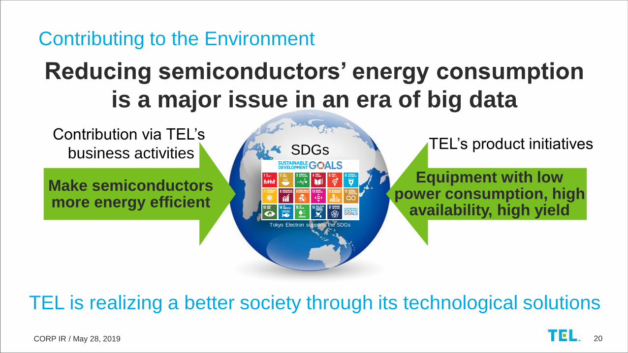
Contributing to the Environment
Reducing semiconductors’ energy consumption
is a major issue in an era of big data
TEL is realizing a better society through its technological solutions
TEL’s product initiativesContribution via TEL’s
business activities
Make semiconductorsmore energy efficient
Equipment with low power consumption, high
availability, high yield
SDGs
Tokyo Electron supports the SDGs
CORP IR / May 28, 2019 21
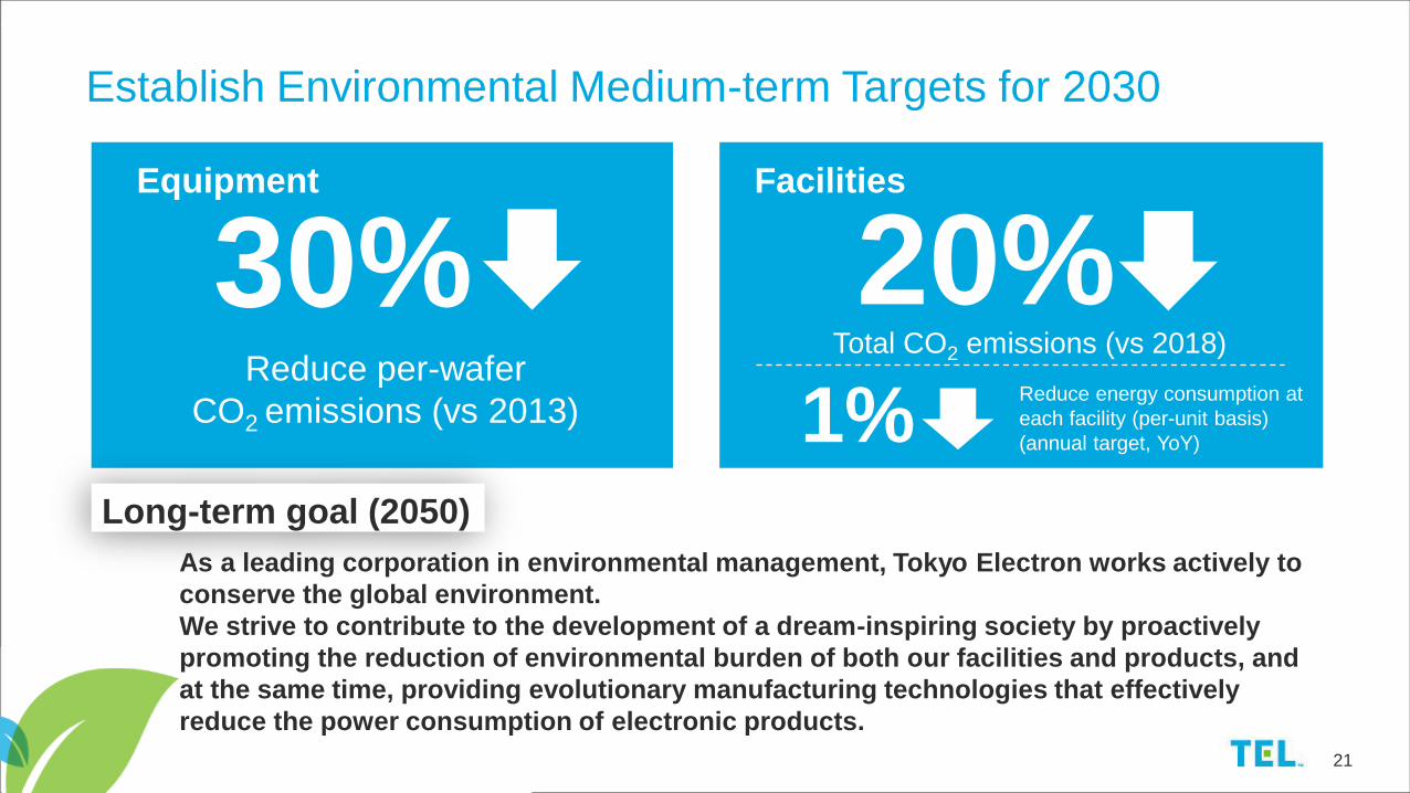
Establish Environmental Medium-term Targets for 2030
21
Total CO2 emissions (vs 2018)Reduce per-wafer
CO2 emissions (vs 2013)
Equipment Facilities
Long-term goal (2050)
30%Reduce energy consumption at
each facility (per-unit basis)
(annual target, YoY)1%
As a leading corporation in environmental management, Tokyo Electron works actively to
conserve the global environment.
We strive to contribute to the development of a dream-inspiring society by proactively
promoting the reduction of environmental burden of both our facilities and products, and
at the same time, providing evolutionary manufacturing technologies that effectively
reduce the power consumption of electronic products.
20%

CORP IR / May 28, 2019 22
Share Repurchase Plan
• Type of shares to be acquired: Shares of common stock
• Total number of shares to be acquired: Up to 14 million shares
(Equivalent to 8.5% of outstanding shares excluding treasury stock)
• Total cost of acquisition: Up to 150 billion yen
• Period of acquisition: From May 28, 2019 to December 31, 2019
Plan to implement share repurchase of up to 150B yen
We will continue to manage our balance sheet flexibly
while considering our ability to generate cash, necessary
cash on hand and growth investment capital

CORP IR / May 28, 2019 23
Revised financial model with aim of further growth
TEL is looking towards future growth, and intends to continue stable
investment. We intend to conduct 400B yen in R&D investment over the
next 3 years
Aim for operating margin and ROE of over 30% in the medium- to long-
term by continually pursuing the best products and best service
Plan to repurchase 150B yen of own shares based on our confidence in
future profit growth
Summary
Aim for sustained growth in corporate value through
a management base with global-standard strength

CORP IR / May 28, 2019 24
May 28, 2019
Akihisa Sekiguchi, Ph.D.
Device Technology GM, Corporate Marketing
The Big Picture: Future of the Electronics Industry

CORP IR / May 28, 2019 25
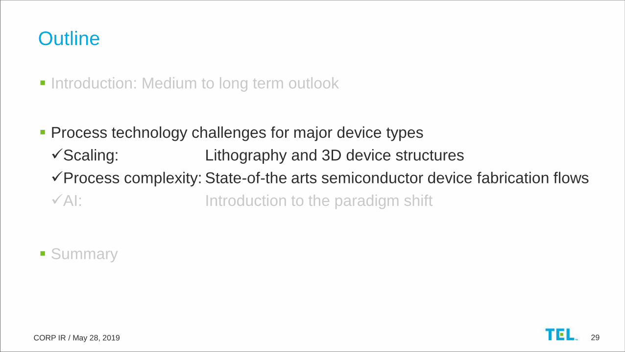
Introduction: Medium to long term outlook
Process technology challenges for major device types
Scaling: Lithography and 3D device structures
Process complexity: State-of-the arts semiconductor device fabrication flows
AI: Introduction to the paradigm shift
Summary
Outline

CORP IR / May 28, 2019 26
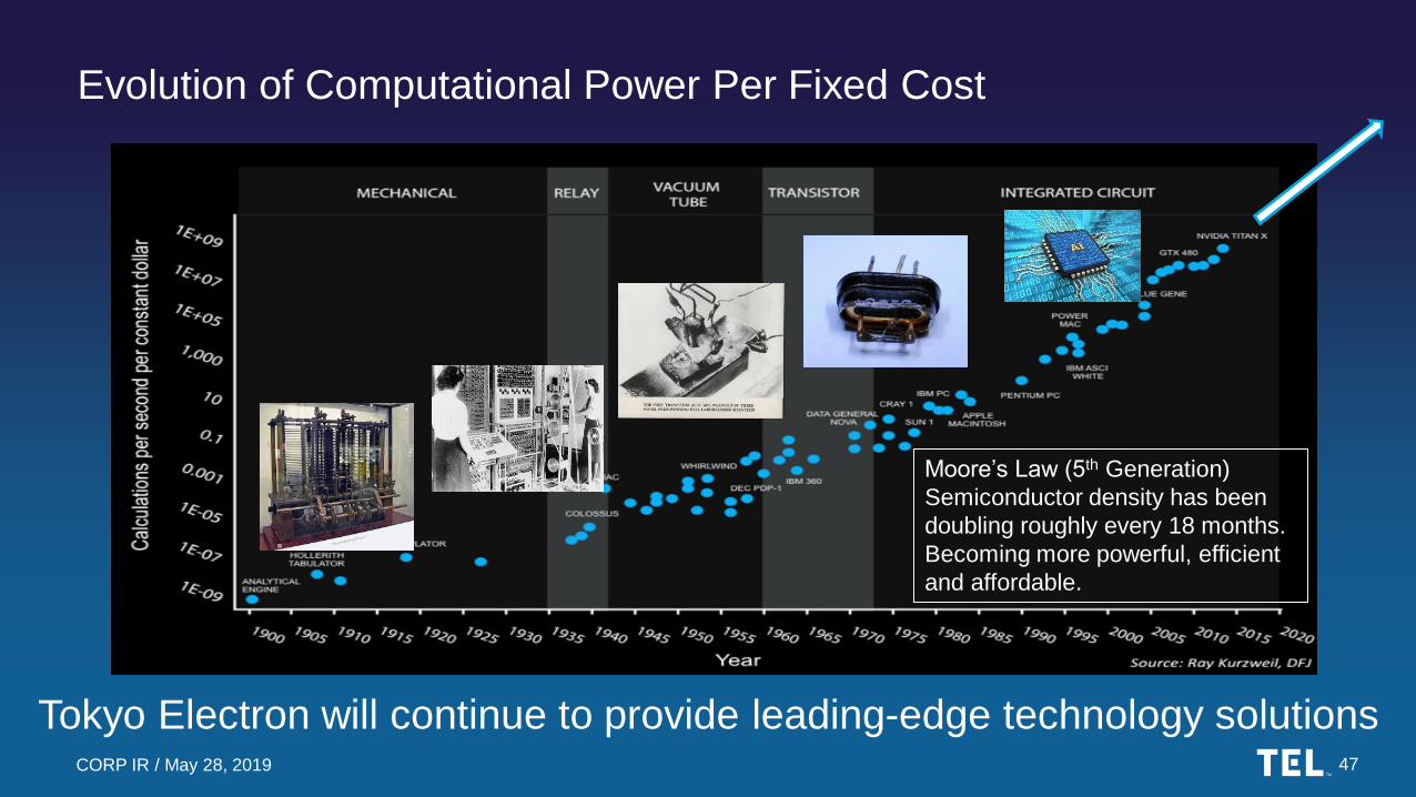
Evolution of Computational Power Per Fixed Cost
Today’s key phrase is PPAC (Power Performance Area Cost)
Moore’s Law (5th Generation)
Semiconductor density has been
doubling roughly every 18 months.
Becoming more powerful, efficient
and affordable.

CORP IR / May 28, 2019 27
Technology Landscape
Mobile
Connected
devices
FinTech
AR/MR/VRCloud
Network
Autonomous
Driving
PC
AI/ML
Robotics
RPA
New application is creating enormous
amounts of data through synergy
Quantum
Computing
Neuromorphic
devices
Medical/DNA
technology

CORP IR / May 28, 2019 28
Mobile Phone Full of Leading-edge Devices
Memory: DRAMWorking memory
Memory: NAND
Storage memory
Logic/MPU
Data processing
CIS Visual
Image sensor
Evolution towards a portable cognitive device with AI chip on boardGate
Gate
FinSTI
Interconnects
Contact
Photodiode
Interconnects
Gate
Color
filter
Pixel isolation
Micro lens
Contact
Channel
Staircase
Word line isolation (Slit)
STI
Capacitor
Buried gateBitline
Contact
Interconnects
CORP IR / May 28, 2019 29
Introduction: Medium to long term outlook
Process technology challenges for major device types
Scaling: Lithography and 3D device structures
Process complexity: State-of-the arts semiconductor device fabrication flows
AI: Introduction to the paradigm shift
Summary
Outline

CORP IR / May 28, 2019 30
Scaling Lead by Lithography Tools
Device evolution has been supported for a long time but…
180130 110 90
6545
3222
14
107
5
1
10
100
1000
1990 1993 1996 1999 2002 2005 2008 2011 2014 2017 2020
Wavelength
Technology node
ArF
EUV
i-ArF
Scaling
KrFi-line
Planar FET
(nm)
Planar NANDPlanar FET

CORP IR / May 28, 2019 31
Material and Structural Innovation
High AR of DRAM
3D NAND
Planar FET
FinFET
GAA FET
3D architecture
3D NAND large stack
New material and 3D devices have also contributed to performance gains

CORP IR / May 28, 2019 32
Performance Enhancement through Scaling, Material Development
and 3D Structures
Architecture, design, process are also being actively investigated
180130 110 90
6545
3222
14
107
5
1
10
100
1000
1990 1993 1996 1999 2002 2005 2008 2011 2014 2017 2020
ArF
EUV
i-ArF
Scaling
KrFi-line
High AR of DRAM
3D NAND
Planar FET
FinFET
GAA FET
3D architecture
(nm)
Planar NANDPlanar FET
3D NAND large stack
Wavelength
Technology node

CORP IR / May 28, 2019 33
0
42.5
85
127.5
170
212.5
0 42.5 85 127.5 170 212.5
Min
. m
eta
l li
ne
wid
th (
ato
ms
)
Patterned gate length (atoms)
The Real Meaning of Scaling
Traditional thinking
N22
N10
N7
N5
N14
Stochastic
effects
Process
control
N22

CORP IR / May 28, 2019 34
0
42.5
85
127.5
170
212.5
0 42.5 85 127.5 170 212.5
Min
. m
eta
l li
ne
wid
th (
ato
ms
)
Patterned gate length (atoms)
Traditional View of Scaling
Nanowire example: HfO2 used for gate oxide is about 140Å3…
Traditional diagram
N22
N10
N7
N5
N14
Stochastic
effects
Process
control
N22

CORP IR / May 28, 2019 35
0
42.5
85
127.5
170
212.5
0 42.5 85 127.5 170 212.5
Min
. m
eta
l li
ne
wid
th (
ato
ms
)
Patterned gate length (atoms)
The Impact of Scaling to Process
High volume manufacturing requires ±10% range process control
In reality
N22
N10
N7
N5
N14
Stochastic
effects
Process
control
N22

CORP IR / May 28, 2019 36
Next Generation Gate-All-Around Transistor (GAA FET)
Leading-edge process enables formation of even complex 3D structuresSource: imec
FinFET Nanowire FET Nanosheet FET
Fabrication flow
of GAA FET

CORP IR / May 28, 2019 37
Fabrication Flows of DRAM, 3D NAND and Logic Device
DRAM 3D NAND Logic
Video

CORP IR / May 28, 2019 38
14/16nm 10nm 7nm 5nm
Logic
4X 6/7X 9X 12X
3D NAND
2Z 1X 1Y 1Z
DRAM
Rising Added-value in SPE
WFE investment (100k WSPM*, greenfield/TEL estimates)
~$7B~$8B
~$20B
* WSPM: Wafer starts per month
Expanding business opportunities for SPE manufacturers on arrival
of new applications and rising level of technological difficulty

CORP IR / May 28, 2019 39
Introduction: Medium to long term outlook
Process technology challenges for major device types
Scaling: Lithography and 3D device structures
Process complexity: State-of-the arts semiconductor device fabrication flows
AI: Introduction to the paradigm shift
Summary
Outline

CORP IR / May 28, 2019 40
Estimated data generation by year in Zettabytes
Increasing Data Generation
0
20
40
60
80
100
120
140
160
180
2010 2015 2020 2025
Source: StorageNewsletter.com white paper (2017)
Data
(Z
ett
abyte
s)
Year
Drivers:
Connecting people connecting devices (IoT):
by 2025 the average person will interact with
connected devices once every 18 seconds,
Metcalfe’s law
Increase in criticality of data: “edge” & “cloud”
Real-time data available instantly anywhere it is
needed (medical, etc.) where latency is an issue
Cognitive systems (AI, ML/DL, language
processing) becomes available at the “edge”
Virtual, Augmented, Mixed Reality (VR/AR/MR)
Information & data security
Autonomous driving, blockchain, etc…
Scale Multiple
giga 109
tera 1012
peta 1015
exa 1018
zetta 1021
yotta 1024
163ZB in 2025
Edge and cloud contribute to the growth of data generation through network

CORP IR / May 28, 2019 41
Data creationsensor
Local data
storage
Local data
analysis
Data upload
Cloud data
storage
Cloud data
analysis
Cloud data
creation
An Example of Data Creation, Storage, Analysis That Leads to
More Data
A variety of algorithms analyze the created data to create even more data
Data creation
Data storage
Data analysis

CORP IR / May 28, 2019 42
Artificial/Augmented Intelligence AI device related development is
accelerating (in particular algorithms
and applications)
Hardware development active but
takes longer time
CY'17 CY'18 CY'19 CY'20 CY'21 CY'22
CAGR 67%
$15.8B
$1.2B
AI devices expected to grow at an annualized rate of almost 70%

CORP IR / May 28, 2019 43
The Future of Computing
“AI will transform the world in dramatic ways in the coming
years. We are creating a global hub of AI hardware research
with an ecosystem to innovate, incubate, and lead in the
development of disruptive technologies.”
Mukesh V. Khare, Ph.D.
Vice President
IBM Research
Era of AI hardware
CORP IR / May 28, 2019 44
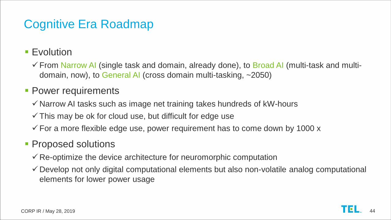
Cognitive Era Roadmap
Evolution
From Narrow AI (single task and domain, already done), to Broad AI (multi-task and multi-
domain, now), to General AI (cross domain multi-tasking, ~2050)
Power requirements
Narrow AI tasks such as image net training takes hundreds of kW-hours
This may be ok for cloud use, but difficult for edge use
For a more flexible edge use, power requirement has to come down by 1000 x
Proposed solutions
Re-optimize the device architecture for neuromorphic computation
Develop not only digital computational elements but also non-volatile analog computational
elements for lower power usage

CORP IR / May 28, 2019 45
Introduction: Medium to long term outlook
Process technology challenges for major device types
Scaling: Lithography and 3D device structures
Process complexity: State-of-the arts semiconductor device fabrication flows
AI: Introduction to the paradigm shift
Summary
Outline

CORP IR / May 28, 2019 46
Electronics industry will continue to grow
Driver is the synergy between the ever increasing data and the
connected devices
Major devices have been evolving over the many decades thanks to the
numerous innovations
Molecular level process control is only possible with leading-edge tools
AI semiconductor which is a new category of device will prompt further
growth of the industry
Summary
CORP IR / May 28, 2019 47
Evolution of Computational Power Per Fixed Cost
Tokyo Electron will continue to provide leading-edge technology solutions
Moore’s Law (5th Generation)
Semiconductor density has been
doubling roughly every 18 months.
Becoming more powerful, efficient
and affordable.

CORP IR / May 28, 2019 48
Technology Enabling Life
Safer mobility
Precision medicine
Ubiquitous education
Technology which contributes to the society
CORP IR / May 28, 2019 49
May 28, 2019
Yoshinobu Mitano
SVP & General Manager, SPE Business Division
SPE Business Market Outlook

CORP IR / May 28, 2019 50
Business Environment and Outlook for TEL’s SAM in the SPE
Business
($B)
Business environment
DRAM– Copper material adopted to lower resistance of
interconnect
– Capacitor formation is the key to continuing scaling
NAND– Multi-layering has reached over 90 layers
– Higher aspect ratio etch, high-productivity sacrificial
film removal and atomic level control in film formation
in 3D structures are crucial for continued increase in
density
Logic/Foundry– Increasing complexity of patterning requires co-
optimization between unit processes
– Adoption of EUV lithography for mass production
TEL’s SAM* in the semiconductor
manufacturing equipment market* TEL forecasts. SAM: Served available market
Coater/Developer Cleaning
Etch Deposition
3.0 3.4 2.9 3.6 3.8 4.01.8 2.2 2.0 2.1 2.4 2.5
10.812.1
10.1
13.315.5 15.8
4.5
5.0
3.9
5.2
5.8 6.1
0
10
20
30
CY'17 CY'18 CY'19 CY'20 CY'21 CY'22
CORP IR / May 28, 2019 51
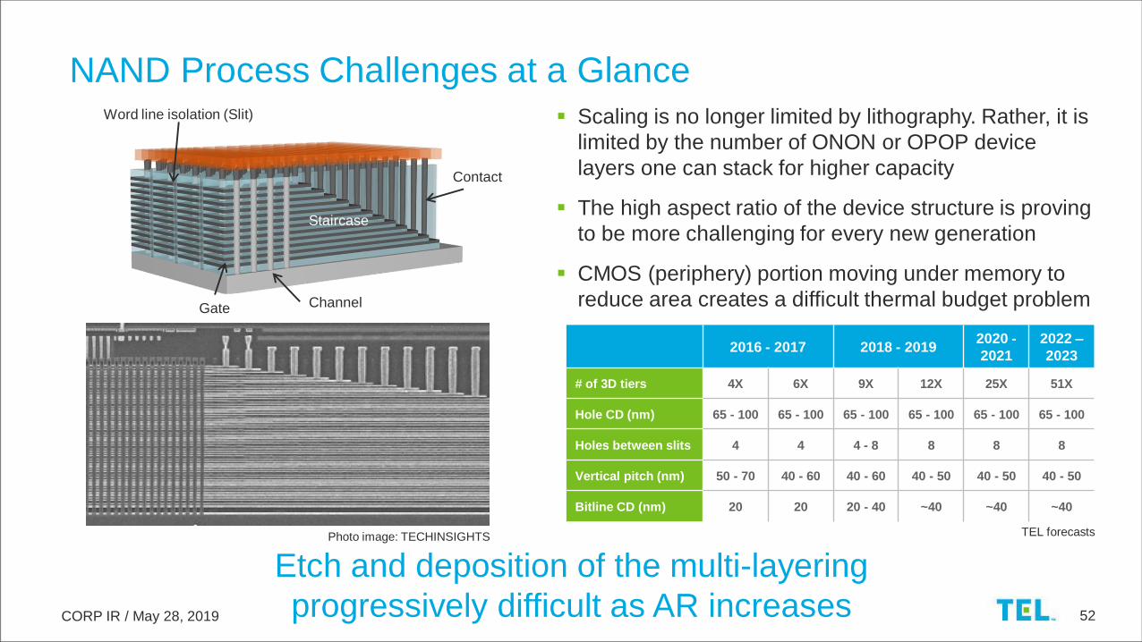
DRAM Process Challenges at a Glance
Scaling increasingly difficult due to capacitor pitch
limitation
– Multi-patterning at Capacitor, WL, BL, STI levels
To scale capacitor EOT, high-k (ZrO2/Al2O/ZrO2)
dielectrics have been introduced with metal (MIM)
CMOS (periphery) portion moving to HKMG* &
FinFETs to reduce area
Capacitors will change from cylinders (dielectric
on outside and in center) to pillars (dielectric on
outside only) with thinner high-k for space saving
– Aspect ratio increases to >50:1 @D16 node
and continues to ~80:1
All aspects of high aspect ratio structure difficult to
fabricate (etch, film deposition, cleaning, …)
STI
Capacitor
Interconnects
Contact
Bitline
Buried gate
Conventional 6F2
cell structure
DRAM faces scaling, materials and integration challenges
* HKMG: High-k metal gate
CORP IR / May 28, 2019 52
NAND Process Challenges at a Glance Scaling is no longer limited by lithography. Rather, it is
limited by the number of ONON or OPOP device
layers one can stack for higher capacity
The high aspect ratio of the device structure is proving
to be more challenging for every new generation
CMOS (periphery) portion moving under memory to
reduce area creates a difficult thermal budget problem
Contact
Channel
Staircase
Word line isolation (Slit)
Gate
Photo image: TECHINSIGHTS
Etch and deposition of the multi-layering
progressively difficult as AR increases
2016 - 2017 2018 - 20192020 -
2021
2022 –
2023
# of 3D tiers 4X 6X 9X 12X 25X 51X
Hole CD (nm) 65 - 100 65 - 100 65 - 100 65 - 100 65 - 100 65 - 100
Holes between slits 4 4 4 - 8 8 8 8
Vertical pitch (nm) 50 - 70 40 - 60 40 - 60 40 - 50 40 - 50 40 - 50
Bitline CD (nm) 20 20 20 - 40 ~40 ~40 ~40
TEL forecasts

CORP IR / May 28, 2019 53
1
12
33 masks
Too close
Closer
Too far
1 mask
Cut
Three exposures: (Litho + Etch) x 3 Lower yield
Increased yield
Placement errors reduced
Cross section of
a logic structure
EUV
introduction
Conventional
exposure
Exposure using
EUV
11
11
Line
Space
Self-aligned multiple patterning (SAMP)
- high etch and dep usage
LELELE = (Litho-Etch)3
- limited etch and dep usage
Step 1: Line/Space
Step 2: Cut
One exposure: (Litho + Etch) x 1
Each exposure process
creates placement errors
Logic: Overcoming Technological Hurdles (Placement Errors)
with EUV

CORP IR / May 28, 2019 54
EUV adoption will solve the technological hurdles our customers face (i.e.
placement errors), bringing about positive effects for the semiconductor and
SPE industries
– Advancement of scaling
– Acceleration of customers’ investment in next generation technologies through yield
enhancement
The advancement of scaling driven by EUV will further differentiate our
products and create business opportunities
– Greater market share for coater/developer
– Increase demand for etch, deposition and cleaning equipment
– Product differentiation driven by evolution of self-aligned patterning technology
– Business expansion through process integration that leverages our robust product line-up
Effects of EUV Lithography Adoption
CORP IR / May 28, 2019 55
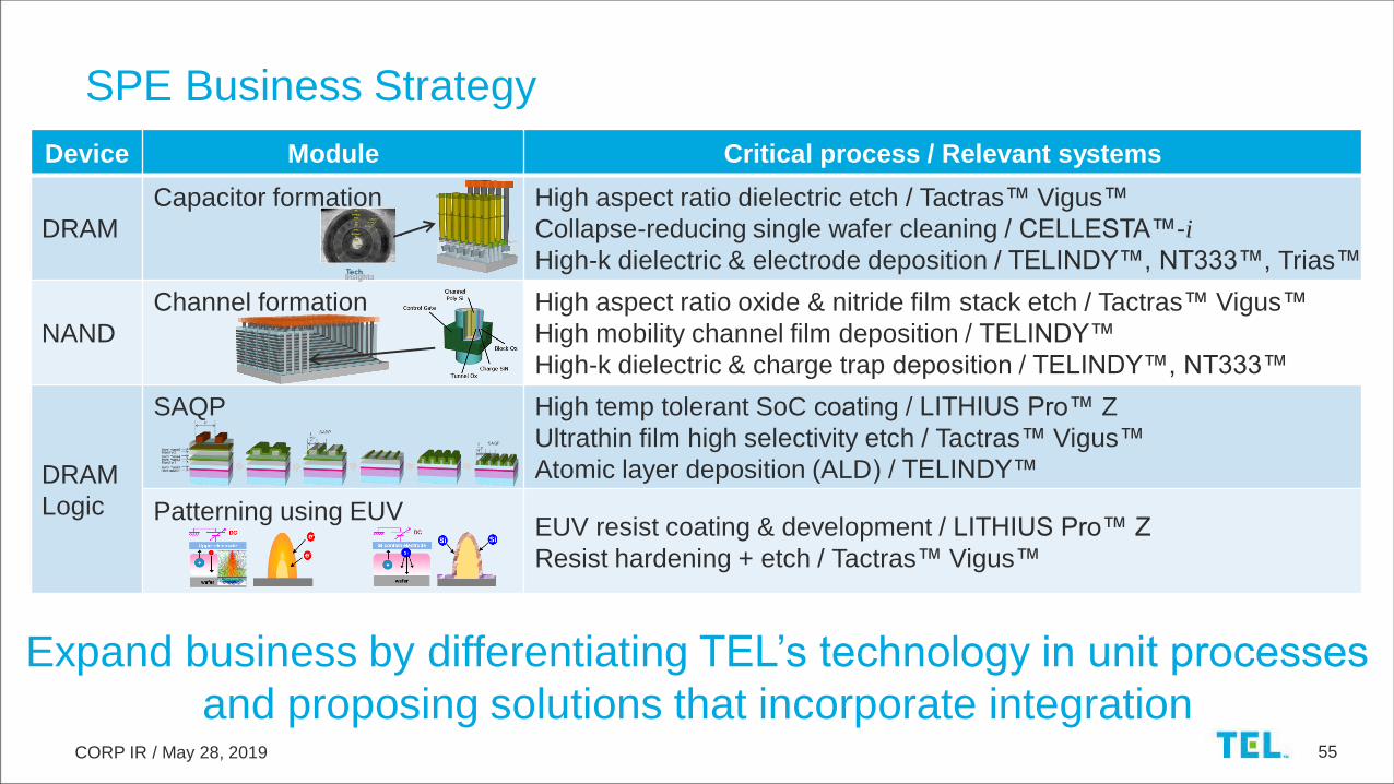
SPE Business Strategy
Device Module Critical process / Relevant systems
DRAM
Capacitor formation High aspect ratio dielectric etch / Tactras™ Vigus™
Collapse-reducing single wafer cleaning / CELLESTA™-i
High-k dielectric & electrode deposition / TELINDY™, NT333™, Trias™
NAND
Channel formation High aspect ratio oxide & nitride film stack etch / Tactras™ Vigus™
High mobility channel film deposition / TELINDY™
High-k dielectric & charge trap deposition / TELINDY™, NT333™
DRAM
Logic
SAQP High temp tolerant SoC coating / LITHIUS Pro™ Z
Ultrathin film high selectivity etch / Tactras™ Vigus™
Atomic layer deposition (ALD) / TELINDY™
Patterning using EUVEUV resist coating & development / LITHIUS Pro™ Z
Resist hardening + etch / Tactras™ Vigus™
Expand business by differentiating TEL’s technology in unit processes
and proposing solutions that incorporate integration

CORP IR / May 28, 2019 56
May 28, 2019
Keiichi Akiyama
VP & General Manager, CTSPS BU
Coater/Developer, Cleaning System Business Strategy

CORP IR / May 28, 2019 57
Business Environment and Outlook for TEL’s SAM in the
Coater/Developer and Cleaning System Businesses
TEL’s SAM in the coater/developer
and cleaning systems markets*($B)
Business environment
Coater/Developer
– Adoption of EUV lithography for mass production
is accelerating
Cleaning system
– Increased demand for bevel cleaning
– Further demand for drying technology that
prevents pattern collapse accompanying scaling
Coater/Developer
CLEAN TRACK™
LITHIUS Pro™ Z
Single wafer cleaning system
CELLESTA™-i
Batch cleaning system
EXPEDIUS™-i
Growth in coater/developer and cleaning systems SAM on demand for
increasing density of semiconductor devices
Coater/
Developer
Cleaning3.0 3.4 2.9 3.6 3.8 4.01.8 2.2 2.0 2.1 2.4 2.5
0
10
20
30
CY'17 CY'18 CY'19 CY'20 CY'21 CY'22
* TEL forecasts

CORP IR / May 28, 2019 58
Coater/Developer
– Grew market share to 88% amid increased ratio of investment in leading-edge processes
– Maintained 100% share in in-line coater/developer for EUV
Cleaning system
– Maintained market share of 25%,
a five-point increased in CY’17
– Enhanced product line-up• Launched CELLESTA™ Pro SPM
– Expanded bevel wet etch applications• Expanded its use in wiring materials (metal)
FY2019 Progress
CELLESTA™ Pro SPM Features
High productivity and availability
High uniformity
Controlled selectivity for metal
Wafer Wafer
Metal
Dielectric
film
Bevel wet etchMetal removal with
high-selectivity

CORP IR / May 28, 2019 59
1.8
2.2
2.02.1
2.42.5
0.0
1.0
2.0
3.0
CY'17 CY'18 CY'19 CY'20 CY'21 CY'22
EUV ArF Immersion ArF KrF i-Line Others
EUV
– Growth in line with progress made on
scaling
ArF Immersion
– Although SAM ratio will gradually fall due to
introduction of EUV, market is the largest
ArF, KrF, i-Line, Others
– SAM ratios will continue to be high due to
expansion of 3D NAND, IoT devices, etc.
Coater/Developer SAM Outlook
Coater/Developer SAM
by light source** TEL forecasts
($B)

CORP IR / May 28, 2019 60
Promote unification of system platforms
– Improve value for customers and unify development
with latest LITHIUS Pro™ Z series
Develop value-added products for scaling
and 3D structures
– Address 3D NAND wafer warpage
Improve quality of service through use of data
and automation
– Promote high-quality support not reliant on technical
skill of personnel
CLEAN TRACK™
LITHIUS Pro™ AP
CLEAN TRACK™
LITHIUS Pro™ Z
3D NAND
Coater/Developer Strategy

CORP IR / May 28, 2019 61
3.0
3.4
2.9
3.63.8
4.0
0.0
1.0
2.0
3.0
4.0
5.0
CY'17 CY'18 CY'19 CY'20 CY'21 CY'22
Single wafer cleaning Batch cleaning Scrubber cleaning
No significant changes to SAM ratios for
cleaning systems
Single wafer cleaning
– Will continue to be the largest market
– Technological innovation aimed at reducing
defects and improving etch/drying performance
will continue
Batch cleaning
– Demand will continue in the market for wet etch
for 3D NAND critical processes
Scrubber cleaning
– The importance of physical back/bevel cleaning
is increasing in pre-lithography process and
other areas
Cleaning System SAM Outlook
($B)
Cleaning system SAM
by system type*
* TEL forecasts

CORP IR / May 28, 2019 62
Single wafer cleaning
– Bevel wet etch• Expect annual market growth rate of around 10%
• Contribute to improving customers’ yields.
Maintain a high market share by differentiating
through performance in precisely removing film from
the outer part of the wafer
– Prevent pattern collapseExpand market share by TEL original technology to
reduce collapse of high aspect ratio pattern
– Metal etchLaunched new dedicated SPM chambers for controlling
selectivity for metal in order to solve reduced yield
issues caused by dry etch damage and residue
Single Wafer Cleaning Strategy
Conventional drying
technologyNew drying technology
Pattern collapses occur No collapse
Metal etch process
Without bevel wet etch With bevel wet etch
W W W WTiN TiN

CORP IR / May 28, 2019 63
Batch and Scrubber Cleaning Strategy SiN etch process
Wafer back and defocus diagram
Wet
etch
Selectivity to SiO2
Uniformity Batch cleaning
– SiN etch and W etch processes for 3D NANDFocus on processes that require long durations
and advanced process technology. Differentiate by
realizing high uniformity, high selectivity and high
productivity in wet etch
Scrubber cleaning
– Pre-lithography processProvide high-value solutions such as reducing
particles brought in by wafers, contributing to the
improvement of exposure tool availability which
have grown increasingly important due to the
introduction of EUV
539
787
1 10
500
1,000
Nitride Oxide
Before
After
Total focus spot count (>50nm)
Small particles
Embedded particles Surface particles

CORP IR / May 28, 2019 64
Cleaning System Growth Scenario
Single wafer cleaning
– Grow sales with pattern collapse reduction
technology and by improving productivity
– Maintain a high market share for bevel wet etch
and expand applications through removal of new
materials
Batch cleaning
– Expand POR in 3D NAND critical processes
Scrubber cleaning
– SAM will grow as importance of back/bevel
processing increases due to introduction of EUV
Aim for 30% SAM share within 5 years
-10%
10%
30%
50%
70%
90%
110%
130%
150%
0.0
1.0
2.0
3.0
4.0
5.0
CY'17 CY'18 CY'19 CY'20 CY'21 CY'22
SAM (in dollars) Single wafer cleaning
Batch cleaning Scrubber
SAM share
25%
* TEL forecasts. SAM shown on a dollar basis and sales on a yen basis
Sales targets by system type within
TEL’s SAM for cleaning systems*

CORP IR / May 28, 2019 65
Coater/Developer
Continue to develop technology that differentiates TEL in leading-edge
technology areas and maintain high value and market share
Cleaning system
Continue to differentiate via technological development, focusing on processes
where customers need a high level of technological support, such as improving
yield
Synergies
Raise efficiency of development and production by sharing BKM* and
promoting unification of development, production and management of
coater/developer and cleaning systems
Summary
* BKM: Best known method

CORP IR / May 28, 2019 66
May 28, 2019
Isamu Wakui
VP & General Manager, ES BU
Etch System Business Strategy

CORP IR / May 28, 2019 67
Business Environment and Outlook for TEL’s SAM in the Etch System
Business
Business environment
Investment in HARC process growing due to
increases in number of 3D NAND layers and
production capacity
Increase in patterning process accompanying
logic scaling
SAM in CY’22 forecast to be 50% greater than
in CY’19
Tactras™ Vigus™ Certas LEAGA™
($B)
TEL’s SAM in the etch systems market*
* TEL forecasts
SAM in the etch business to continue growing due to increase in
HARC and patterning processes
10.812.1
10.1
13.315.5 15.8
0
10
20
30
CY'17 CY'18 CY'19 CY'20 CY'21 CY'22
Etch

CORP IR / May 28, 2019 68
Achieved medium-term market share target of 30% in CY’18 by focusing on
HARC process, patterning process and interconnect process, all of which
leverage TEL’s strengths
Expanded market share in 3D NAND 6X/9X generations by differentiating
through process performance and productivity
Increased sales in DRAM copper interconnect process, where we captured
market share by leveraging knowledge of logic
FY2019 Progress

CORP IR / May 28, 2019 69
FY2019 Progress
Video
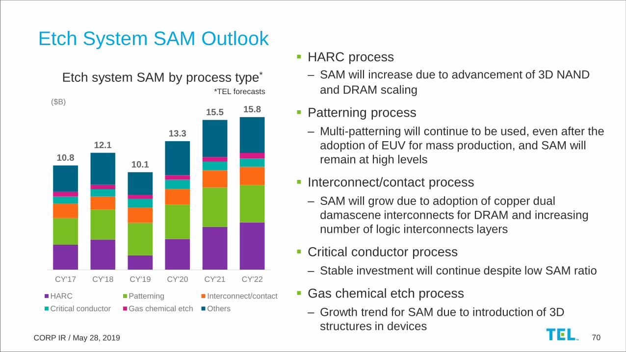
CORP IR / May 28, 2019 70
HARC process
– SAM will increase due to advancement of 3D NAND
and DRAM scaling
Patterning process
– Multi-patterning will continue to be used, even after the
adoption of EUV for mass production, and SAM will
remain at high levels
Interconnect/contact process
– SAM will grow due to adoption of copper dual
damascene interconnects for DRAM and increasing
number of logic interconnects layers
Critical conductor process
– Stable investment will continue despite low SAM ratio
Gas chemical etch process
– Growth trend for SAM due to introduction of 3D
structures in devices
Etch System SAM Outlook
10.8
12.1
10.1
13.3
15.5 15.8
0.0
1.0
2.0
3.0
4.0
5.0
6.0
7.0
8.0
9.0
10.0
11.0
12.0
13.0
14.0
15.0
16.0
17.0
18.0
19.0
20.0
CY'17 CY'18 CY'19 CY'20 CY'21 CY'22
HARC Patterning Interconnect/contact
Critical conductor Gas chemical etch Others
*TEL forecasts
($B)
Etch system SAM by process type*

CORP IR / May 28, 2019 71
HARC process– 3D NAND (multi-level contact, word line isolation), DRAM (capacitor):
Continue to differentiate through process performance and productivity
– 3D NAND (channel): Launch new systems that can
differentiate by providing both precise process controllability
and even higher productivity
Patterning process– DRAM: Reduce customer production costs by combining
etch steps
– Logic: Differentiate through integration of etch and deposition
technologies
Interconnect/contact process– Apply knowledge cultivated in logic to DRAM
Gas chemical etch process
– Create a new market through plasma assist technology
Etch System Strategy
Word line
isolation (slit)Channel
Multi-level
contact
Capacitor
Interconnects
Isotropic etch
Nanosheet image:
Courtesy of IBM
Source: N. Loubet, et al., Stacked Nanosheet Gate-All-Around Transistor to Enable Scaling Beyond FinFET
CORP IR / May 28, 2019 72
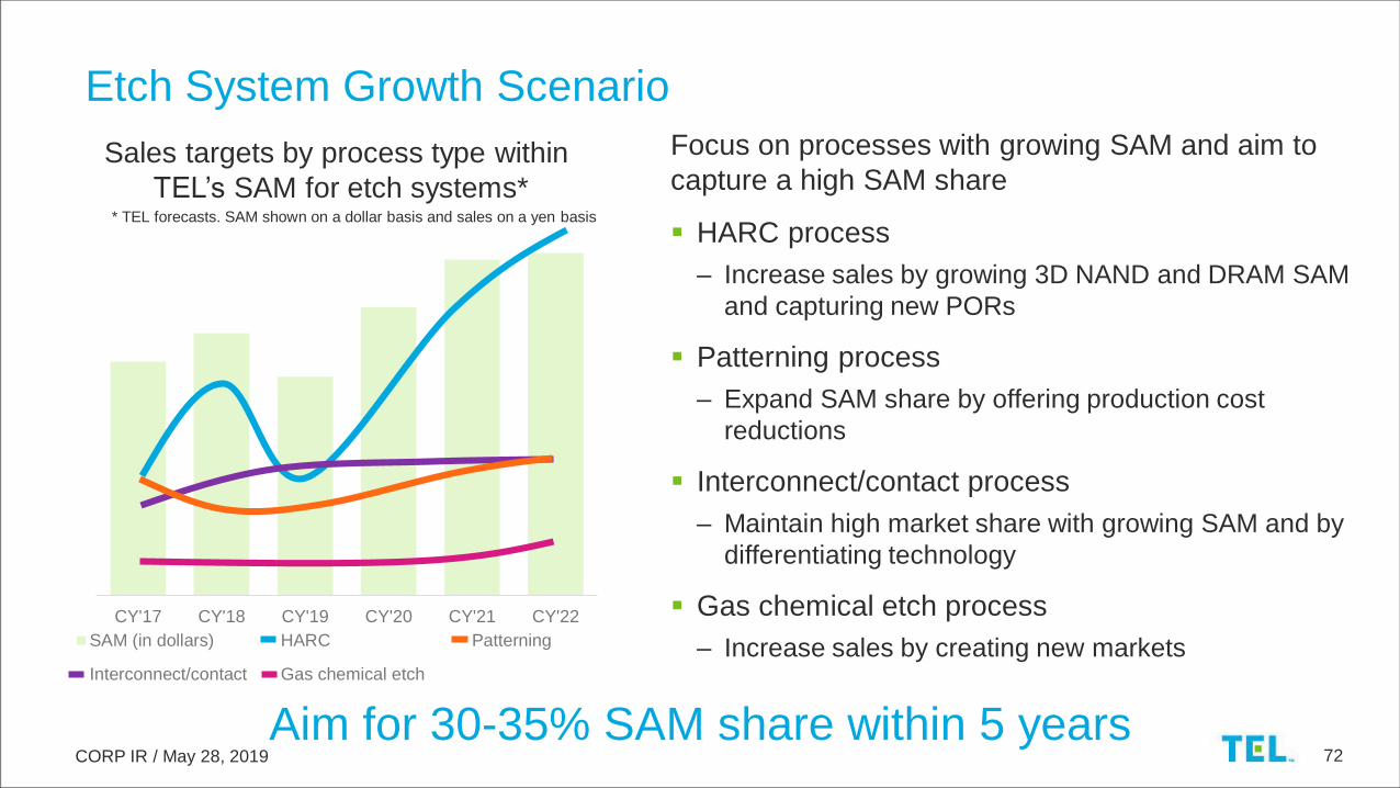
Etch System Growth Scenario
Focus on processes with growing SAM and aim to
capture a high SAM share
HARC process
– Increase sales by growing 3D NAND and DRAM SAM
and capturing new PORs
Patterning process
– Expand SAM share by offering production cost
reductions
Interconnect/contact process
– Maintain high market share with growing SAM and by
differentiating technology
Gas chemical etch process
– Increase sales by creating new markets
0
500
1000
1500
2000
2500
3000
3500
0.0
1.0
2.0
3.0
4.0
5.0
6.0
7.0
8.0
9.0
10.0
11.0
12.0
13.0
14.0
15.0
16.0
17.0
18.0
19.0
20.0
CY'17 CY'18 CY'19 CY'20 CY'21 CY'22
SAM (in dollars) HARC Patterning
Interconnect/contact Gas chemical etch
Sales targets by process type within
TEL’s SAM for etch systems** TEL forecasts. SAM shown on a dollar basis and sales on a yen basis
Aim for 30-35% SAM share within 5 years

CORP IR / May 28, 2019 73
SAM in the etch business to continue growing due to increase in HARC and
patterning processes
Achieved medium-term market share target of 30% in CY’18 by focusing on
HARC process, patterning process and interconnect process, all of which
leverage TEL’s strengths
Focus on processes with growing SAM and aim to capture a high SAM share
Summary

CORP IR / May 28, 2019 74
May 28, 2019
Hiroyuki Ishida
VP & GM, TFF BU
Deposition System Business Strategy

CORP IR / May 28, 2019 75
Business Environment and Outlook for TEL’s SAM in the Deposition
System Business
NT333™
TELINDY PLUS™
Triase+™
Business environment
Increasingly scaled and complex device structures are
increasing the number of deposition processes. In
particular, demand for ALD, which has excellent
performance, is growing
Customers are choosing the most appropriate
technology for each process among batch, semi-batch
and single wafer to balance performance and cost
The number of deposition processes is increasing as device structures become
increasingly scaled and complex. Demand for ALD in particular is growing
4.5
5.0
3.9
5.2
5.8 6.1
0
10
20
30
CY'17 CY'18 CY'19 CY'20 CY'21 CY'22
($B)
TEL’s SAM in the deposition
systems market** TEL forecasts. TEL’s SAM: Diffusion furnaces, semi-batch
ALD system, metal CVD system
Deposition

CORP IR / May 28, 2019 76
Streamlined production, meeting strong demand for systems
Successfully captured business in the memory market, which experienced particularly high
demand, thereby growing market share
Secured business in multiple new functional film processes of major customers
Started construction of new production buildings at the Yamanashi (Fujii) and Tohoku plants
in response to growing market for deposition systems
FY2019 Progress
New building at
the Tohoku plant
New building at the
Yamanashi (Fujii) plant
CORP IR / May 28, 2019 77
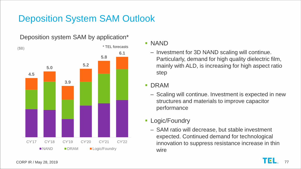
Deposition System SAM Outlook
Deposition system SAM by application*
4.5
5.0
3.9
5.2
5.86.1
0.0
1.0
2.0
3.0
4.0
5.0
6.0
7.0
CY'17 CY'18 CY'19 CY'20 CY'21 CY'22
NAND DRAM Logic/Foundry
NAND
– Investment for 3D NAND scaling will continue.
Particularly, demand for high quality dielectric film,
mainly with ALD, is increasing for high aspect ratio
step
DRAM
– Scaling will continue. Investment is expected in new
structures and materials to improve capacitor
performance
Logic/Foundry
– SAM ratio will decrease, but stable investment
expected. Continued demand for technological
innovation to suppress resistance increase in thin
wire
($B) * TEL forecasts

CORP IR / May 28, 2019 78
Dia: 20nm, AR = 50:1
To
pB
ott
om
Deposition Business Strategy
• Lower temperatures
• High-k dielectric film
• Capacitor electrode
DRAM 3D NAND• Channel silicon film
• Charge trap film
• Block high-k dielectric film
• Buried oxide film
• Buried silicon film
TELINDY PLUSTM Super Large Batch
100/125 150/175
NT333TM
N2
N2
Si precursor
Oxidation
Modification
Triase+™ EX-II ProTM TiN
S/C >95%
Gap-fill SiO2 Dep
Provide high value-added technology by leveraging our
advantage of having batch, semi-batch and single wafer
technologies
Vertical Furnace Semi-batch SystemSingle-wafer System
Equipmentstability
Improved productivity/coverage
Highertempera-
ture
Continuousthin film/
film qualityimprovement
AR ≃ 16:1

CORP IR / May 28, 2019 79
Expand business by choosing the most
appropriate method among batch, semi-batch
and single wafer, and providing high value-
added technologies
In deposition technologies, which are becoming
increasingly advanced, accelerate development
of new materials and new deposition method by
leveraging our strengths. Aim for further growth
– Deposition of new metal material to achieve lower
resistance
– New deposition methods to promote scaling, such
as anisotropic deposition and selective deposition
– Pre-treatment technology to realize better electric
characteristics
Deposition System Growth Scenario
Focus on high value-added deposition processes,
aim for 40%+ SAM share within 5 years
0
20000
40000
60000
80000
100000
120000
140000
160000
0.0
1.0
2.0
3.0
4.0
5.0
CY'17 CY'18 CY'19 CY'20 CY'21 CY'22
SAM (in dollars) DRAM NAND Logic/Foundry Others
Sales targets by application within
TEL’s SAM for deposition systems** TEL forecasts. SAM shown on a dollar basis and sales on a yen basis
CORP IR / May 28, 2019 80
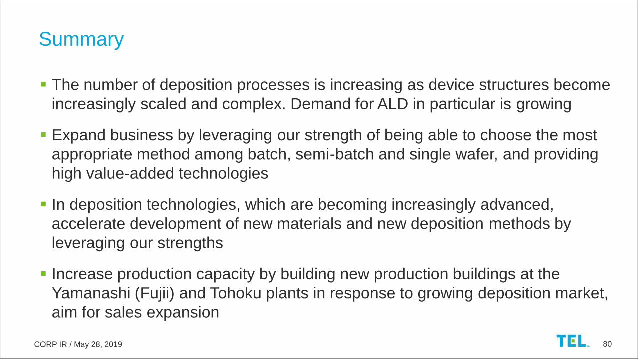
The number of deposition processes is increasing as device structures become
increasingly scaled and complex. Demand for ALD in particular is growing
Expand business by leveraging our strength of being able to choose the most
appropriate method among batch, semi-batch and single wafer, and providing
high value-added technologies
In deposition technologies, which are becoming increasingly advanced,
accelerate development of new materials and new deposition methods by
leveraging our strengths
Increase production capacity by building new production buildings at the
Yamanashi (Fujii) and Tohoku plants in response to growing deposition market,
aim for sales expansion
Summary

CORP IR / May 28, 2019 81
May 28, 2019
Tsuguhiko Matsuura
VP & GM, FPD Business Division
FPD Business Strategy

CORP IR / May 28, 2019 82
Display Trends
Increasing screen size
Increasing resolution
FHD 4K 8K
OLED
Design flexibility
LCD OLED
TFT
Color filter
Backlight
LCD
TFT
Emissive
layer
Flexible, free format
TV
Mobile, VR 300 ppi 1,000 ppi
Technological change in displays increasing business opportunities

CORP IR / May 28, 2019 83
Display Evolution and Diversification of Process Technology
Advanced patterning
New structure/material New display
methods
Flexible
Foldable
Edge bending
μLED
Mini LED
Enhance light extraction efficiency
QLED
OLED
Top emission/TFE
IGZO、LTPO
Top gate/BCE
Capacitance increase/low leak current<1.0μm
Nanoimprint
Direct writing Larger panel size
FPD
manufactu-
ring technology
Diverse new technologies will enable display evolution

CORP IR / May 28, 2019 84
6.6
5.14.7
5.6
4.5
5.0
CY'17 CY'18 CY'19 CY'20 CY'21 CY'22
Coater/Developer Dry etch AMOLED
Business Environment and Outlook for TEL’s SAM in the FPD
business
Business environment
Resolution in large displays increasing, OLED
market expanding
Evolution of mobile displays
($B)
Data based on IHS Markit, Technology Group, Display Supply Demand Equipment Tracker Q4 2018.
Results are not an endorsement of Tokyo Electron Limited. Any reliance on these results is at the third party’s
own risk. Visit technology.ihs.com for more details.
TEL’s SAM in FPD manufacturing
equipment market
Technological innovation continues mainly in large displays
and mobile displays
FPD coater/developer
Exceliner™
FPD plasma etch/ash system
Impressio™
Inkjet printing system for
manufacturing OLED panels
Elius™

CORP IR / May 28, 2019 85
FY2019 Progress
FPD coater/developer
Exceliner™
FPD plasma etch/ash system
Impressio™
Inkjet printing system for
manufacturing OLED panels Elius™
* PICP: Plasma source for producing extremely uniform high-density plasma on substrate
Achieved medium-term operating margin target of 20%
Established a leading position in G10.5
PICP™* etch system product development steady
Launched Elius™ 1000 G4.5 inkjet printing system for manufacturing OLED
panels, which accommodates high resolution

CORP IR / May 28, 2019 86
OLED TV market will further grow. 8K TV market will launch
Mark shift to OLED in high-end monitors, automotive displays and public displays
Business Opportunity: Increasing Resolution in Large Displays,
Growth of OLED TV Market
0
2,000
4,000
6,000
8,000
CY'16 CY'17 CY'18 CY'19 CY'20 CY'21
OLED TV (units)(K units)
Data based on IHS Markit, Technology Group, Display Long-Term Demand Forecast Tracker Q4 2018.
Results are not an endorsement of Tokyo Electron Limited. Any reliance on these results is at the third
party’s own risk. Visit technology.ihs.com for more details.
Promote development activities that reflect technological
trends in large panels
Deploy PICP™ plasma etch system in
G8.5/G10.5
Launch inkjet printing system accommodating
high resolution (200 ppi and above)
Growth strategy

CORP IR / May 28, 2019 87
High resolution, full-screen, OLED, embedded fingerprint sensors, lower power
consumption, foldable
Business Opportunity: Evolution of Mobile Displays
Opportunities for differentiation will expand as technological requirement
becomes more sophisticated
Increase number of masks and dry etch processes
Scaling and patterning precision improvement is
required. Respond to LTPS and IGZO
Improve performance of dry etch system and
coater/developer. Introduce SPE technologies
Business strategy
CORP IR / May 28, 2019 88
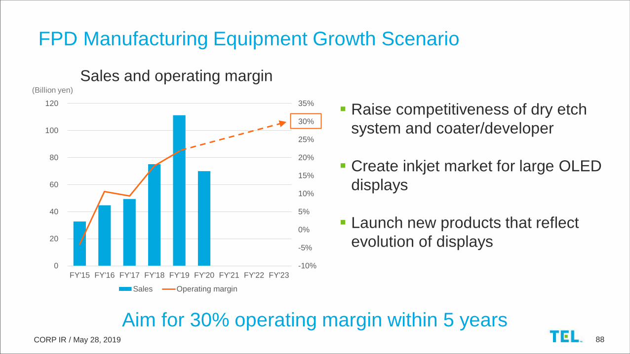
FPD Manufacturing Equipment Growth Scenario
Sales and operating margin(Billion yen)
Raise competitiveness of dry etch
system and coater/developer
Create inkjet market for large OLED
displays
Launch new products that reflect
evolution of displays
-10%
-5%
0%
5%
10%
15%
20%
25%
30%
35%
0
20
40
60
80
100
120
FY'15 FY'16 FY'17 FY'18 FY'19 FY'20 FY'21 FY'22 FY'23
Sales Operating margin
Aim for 30% operating margin within 5 years

CORP IR / May 28, 2019 89
Increase market share and profitability in growing market. Aim for 30%
operating margin
Focus on areas in cutting-edge manufacturing processes where we can
leverage our technological advantages
– Raise competitiveness of dry etch system and coater/developer
– Create inkjet market for large OLED displays
– Launch new products that reflect evolution of displays
Summary

CORP IR / May 28, 2019 90
May 28, 2019
Kiyoshi Sunohara
Corporate Director, SVP & General Manager, Field Solutions Business Division
Subleader, Business Innovation Project
Field Solutions Business Strategy
CORP IR / May 28, 2019 91
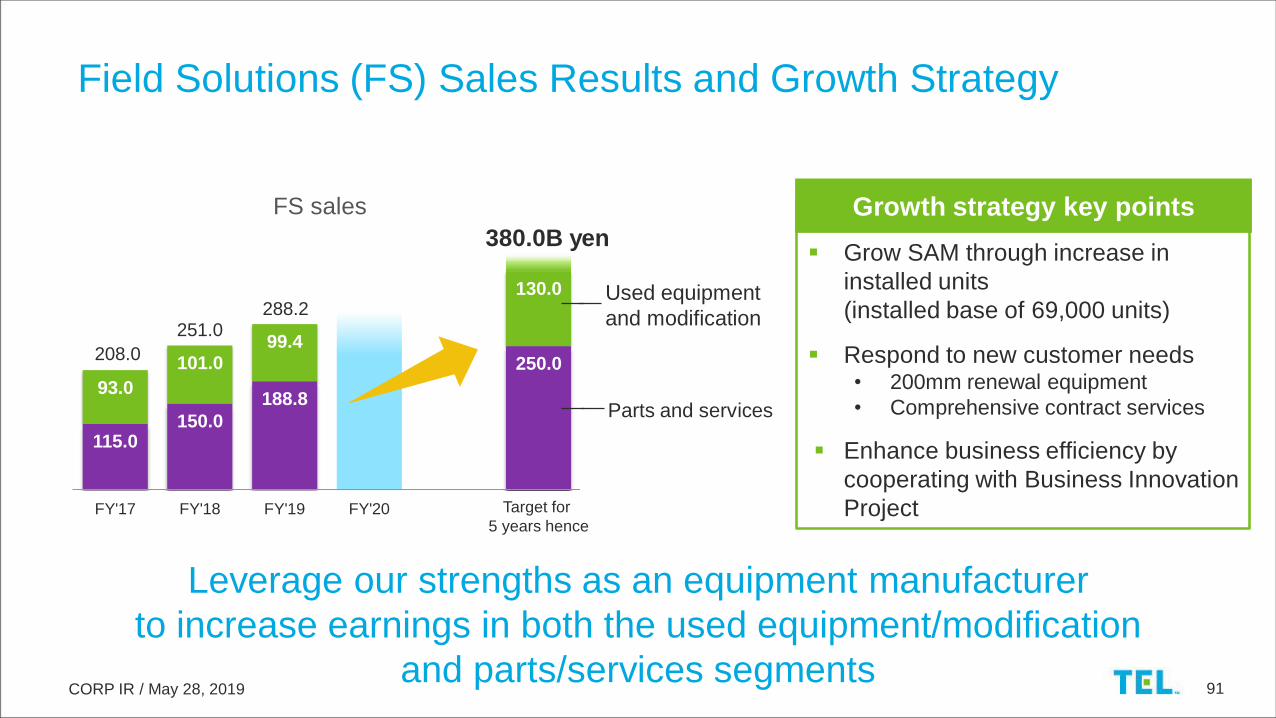
115.0150.0
188.8
250.0
93.0
101.099.4
130.0
0
FY'17 FY'18 FY'19 FY'20
FS sales
Grow SAM through increase in
installed units
(installed base of 69,000 units)
Respond to new customer needs• 200mm renewal equipment
• Comprehensive contract services
Enhance business efficiency by
cooperating with Business Innovation
Project
Used equipment
and modification
Parts and services
Growth strategy key points
Field Solutions (FS) Sales Results and Growth Strategy
380.0B yen
208.0
251.0288.2
Leverage our strengths as an equipment manufacturer
to increase earnings in both the used equipment/modification
and parts/services segments
Target for
5 years hence

CORP IR / May 28, 2019 92
200mm renewal equipment
– Diffusion furnaces, deposition system
– Cleaning system
– Etch system
– Coater/Developer
Capture power device market
– SiC etch
– SiC epitaxial deposition
Used Equipment/Modification Business
Automotive, smartphones, sensors, MEMS, communications markets growing
0
20
40
60
CY'20 CY'21 CY'22 CY'23 CY'24 CY'25 CY'30
Power device market*
Power all Power MOS IGBT SiC
($B)* TEL forecasts
CORP IR / May 28, 2019 93
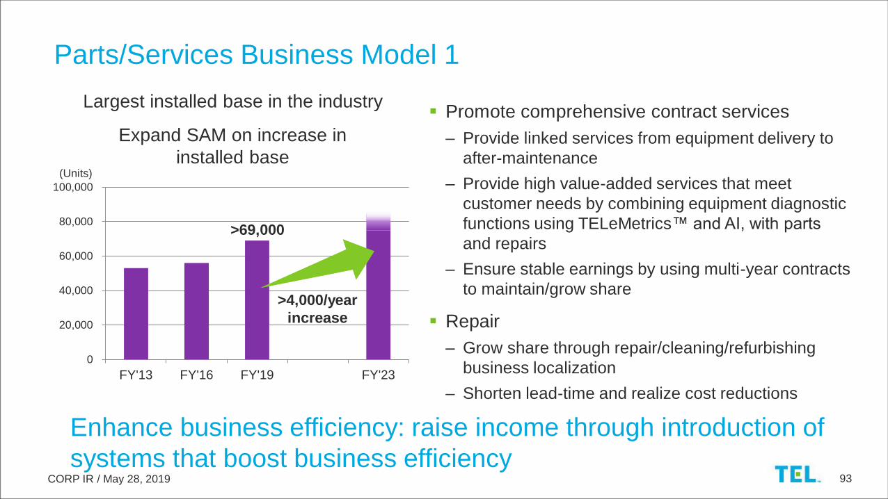
Largest installed base in the industry
Expand SAM on increase in
installed base
Parts/Services Business Model 1
Promote comprehensive contract services
– Provide linked services from equipment delivery to
after-maintenance
– Provide high value-added services that meet
customer needs by combining equipment diagnostic
functions using TELeMetrics™ and AI, with parts
and repairs
– Ensure stable earnings by using multi-year contracts
to maintain/grow share
Repair
– Grow share through repair/cleaning/refurbishing
business localization
– Shorten lead-time and realize cost reductions
Enhance business efficiency: raise income through introduction of
systems that boost business efficiency
0
20,000
40,000
60,000
80,000
100,000
FY'13 FY'16 FY'19 FY'23
>69,000
(Units)
>4,000/year
increase
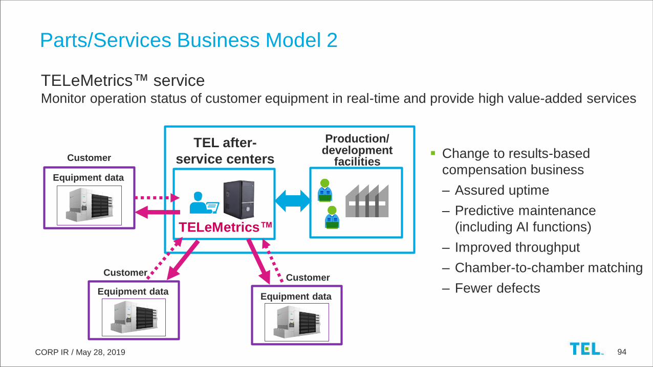
CORP IR / May 28, 2019 94
Equipment data
TEL after-
service centersCustomer
Equipment data
Customer
Equipment data
Production/ development
facilities
TELeMetrics™ serviceMonitor operation status of customer equipment in real-time and provide high value-added services
Parts/Services Business Model 2
Change to results-based
compensation business
– Assured uptime
– Predictive maintenance
(including AI functions)
– Improved throughput
– Chamber-to-chamber matching
– Fewer defects
TELeMetrics™
Customer

CORP IR / May 28, 2019 95
Respond to expansion in SAM on increase in installed base
Grow used equipment/modification business
Promote comprehensive contract services
Enhance business efficiency
Summary
115.0150.0
188.8
250.0
93.0
101.099.4
130.0
0
FY'17 FY'18 FY'19 FY'20
FS sales
Used equipment
and modification
Parts and services
380.0B yen
208.0251.0
288.2
Target for
5 years hence

CORP IR / May 28, 2019 96