memory basics (morris mano – chapter...
TRANSCRIPT
Memory Basics (Morris Mano – Chapter 9)
• Basic Concepts• Address/Data/Control Lines
Read/Write Operations• Read/Write Operations• Read Only Memory (ROM)
– Programmable ROMg– ROM Look-up Tables
• Random Access Memory (RAM)M Add Si E i• Memory Address Size Expansion
ACOE201 1
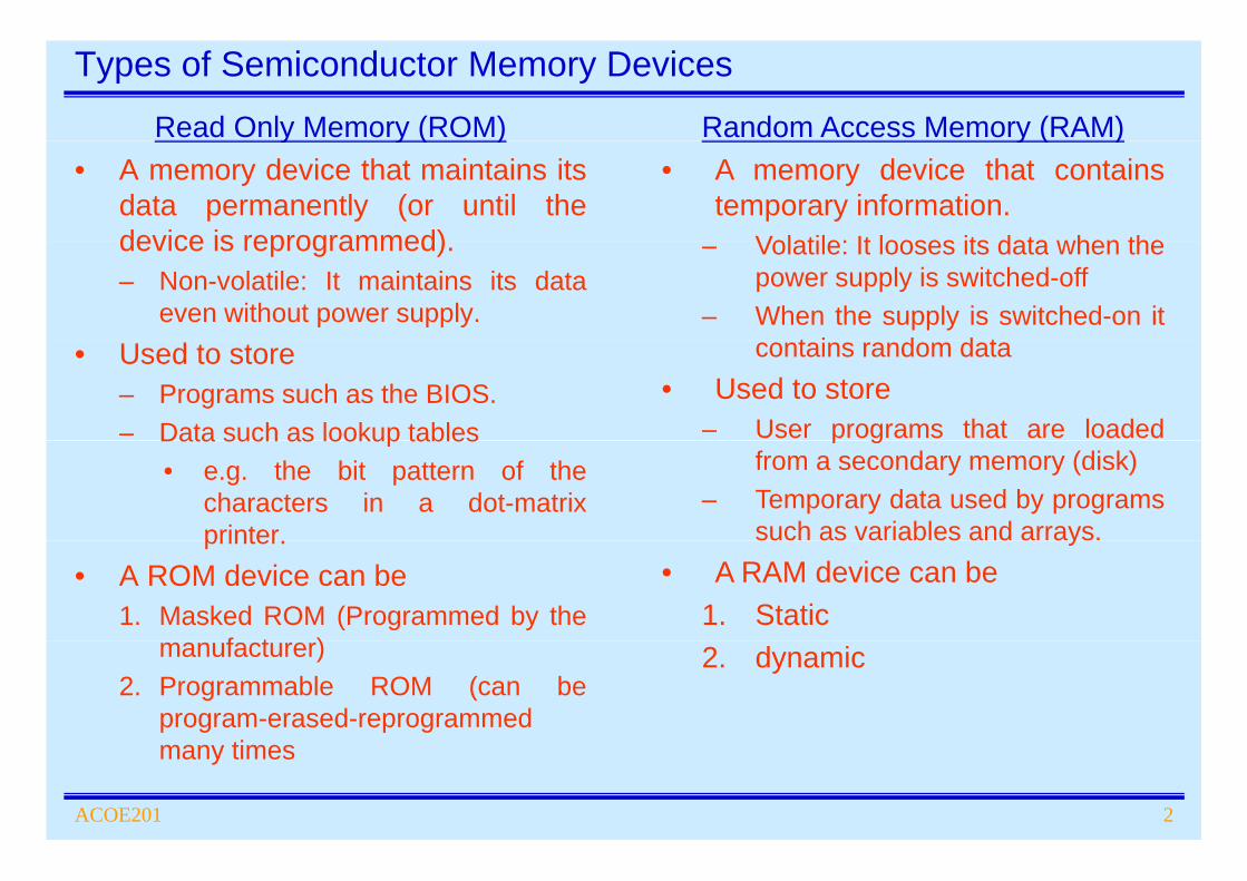
Types of Semiconductor Memory Devices
Read Only Memory (ROM) Random Access Memory (RAM)y y ( )• A memory device that maintains its
data permanently (or until thedevice is reprogrammed)
y ( )• A memory device that contains
temporary information.Volatile: It looses its data when thedevice is reprogrammed).
– Non-volatile: It maintains its dataeven without power supply.
– Volatile: It looses its data when thepower supply is switched-off
– When the supply is switched-on itt i d d t• Used to store
– Programs such as the BIOS.– Data such as lookup tables
contains random data• Used to store
– User programs that are loadedData such as lookup tables• e.g. the bit pattern of the
characters in a dot-matrixprinter
p gfrom a secondary memory (disk)
– Temporary data used by programssuch as variables and arrays.printer.
• A ROM device can be1. Masked ROM (Programmed by the
f t )
y• A RAM device can be
1. Staticmanufacturer)
2. Programmable ROM (can beprogram-erased-reprogrammed
ti
2. dynamic
ACOE201 2
many times
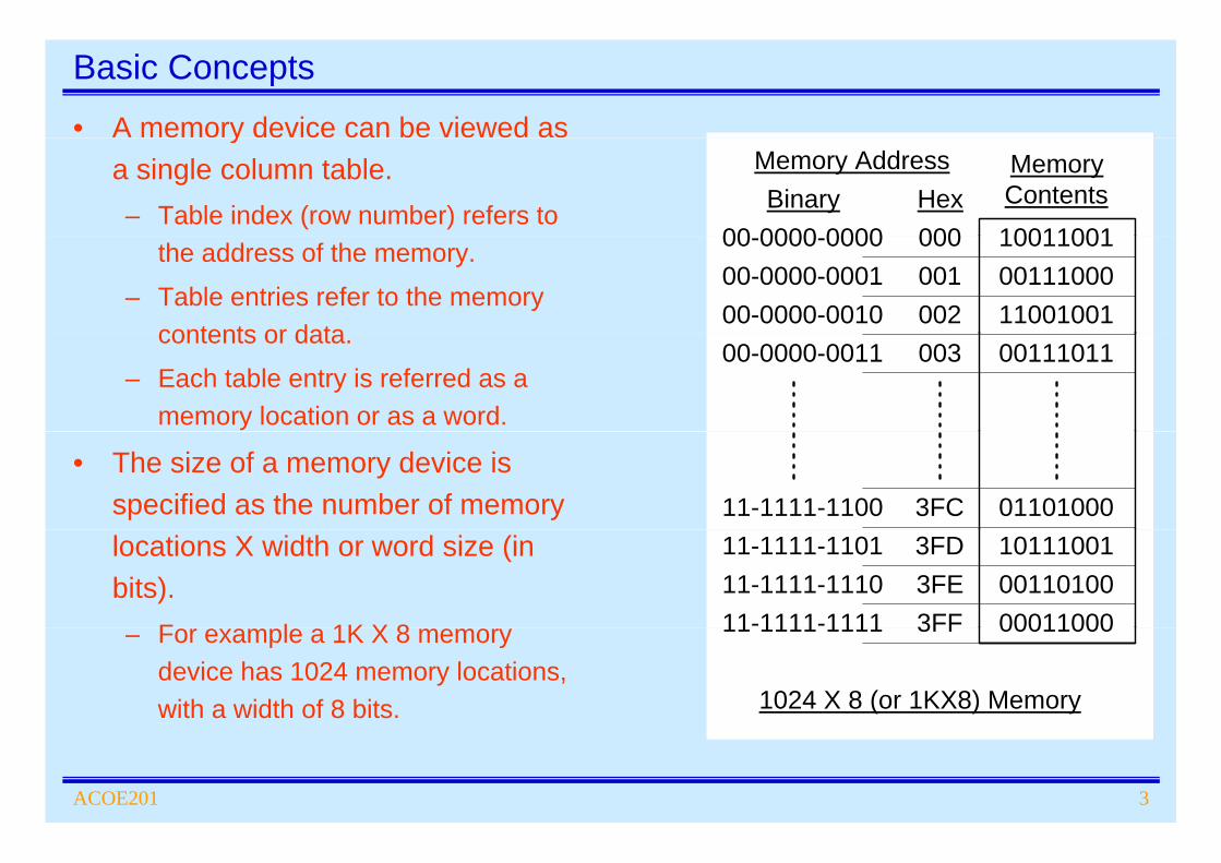
Basic Concepts
• A memory device can be viewed as ya single column table.– Table index (row number) refers to
000Hex
MemoryContents1001100100 0000 0000
Memory AddressBinary
the address of the memory.
– Table entries refer to the memory contents or data
000001002
1001100100111000
00-0000-000000-0000-000100-0000-0010 11001001
contents or data.
– Each table entry is referred as a memory location or as a word.
00300-0000-0011 00111011
• The size of a memory device is specified as the number of memory 3FC11-1111-1100 01101000locations X width or word size (in bits).
F l 1K X 8
3FD3FE
11-1111-110111-1111-111011-1111-1111 3FF
101110010011010000011000– For example a 1K X 8 memory
device has 1024 memory locations, with a width of 8 bits.
11 1111 1111 3FF 00011000
1024 X 8 (or 1KX8) Memory
ACOE201 3
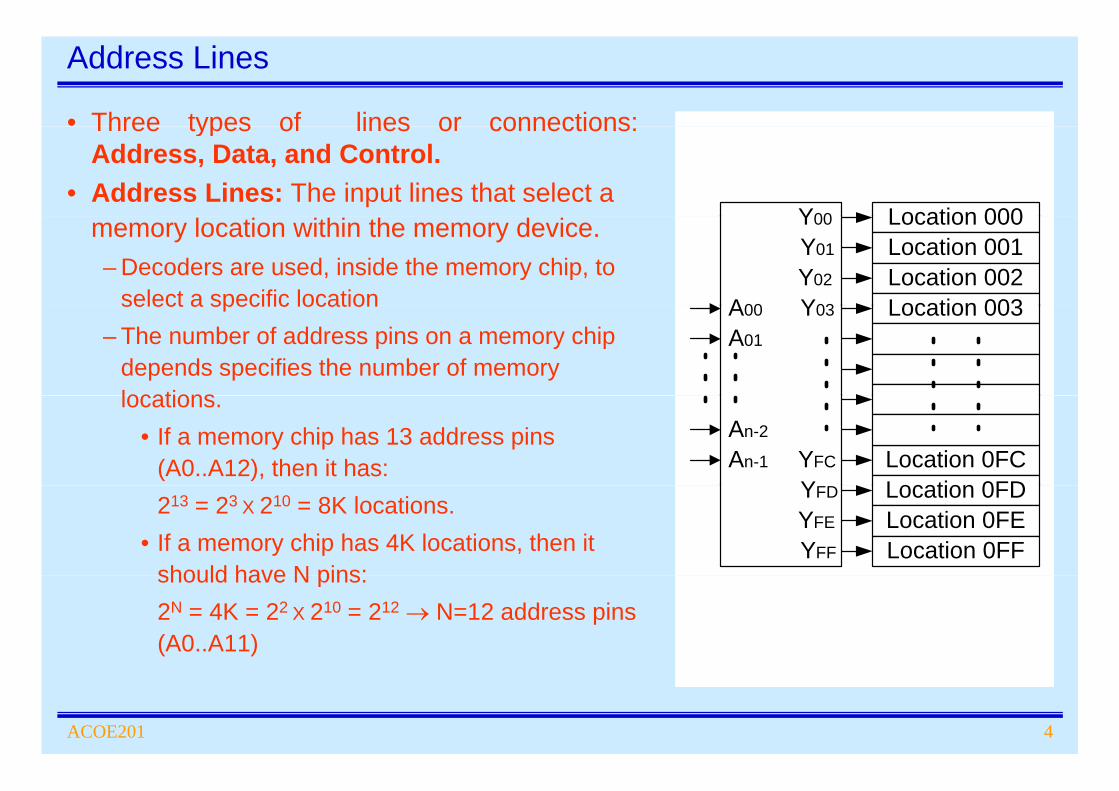
Address Lines
• Three types of lines or connections:Three types of lines or connections:Address, Data, and Control.
• Address Lines: The input lines that select a Location 000Y00memory location within the memory device.
– Decoders are used, inside the memory chip, to select a specific location
Location 000Location 001Location 002Location 003
Y00
Y01
Y02
Y03A00select a specific location– The number of address pins on a memory chip
depends specifies the number of memory locations
Location 003Y03A00
A01
locations.• If a memory chip has 13 address pins
(A0..A12), then it has: Location 0FCLocation 0FD
YFC
Y
An-2
An-1
213 = 23 X 210 = 8K locations.• If a memory chip has 4K locations, then it
should have N pins:
Location 0FDLocation 0FELocation 0FF
YFD
YFE
YFFshould have N pins: 2N = 4K = 22 X 210 = 212 → N=12 address pins (A0..A11)
ACOE201 4

Data Lines
• Data Connections: All memory devices have a set of data output pins (for ROM y p p (devices), or input/output pins (for RAM devices).–Most RAM chips have common bi-directional I/O connections. –Most memory devices have 1, 8 or 16 data lines.
Data Input Lines(DI0..DIn-1)
k- address lines2m d
k- address lines2m dk- address lines
(A0..Am-1)
n-bits perd
Read (RD)Write (WR)
2m words(A0..Am-1)
n-bits perword
Read/Write (R/W)Chip Select (CS)
2m words (A0..Am-1)
n-bits perword
Output Enable (OE)Chip Select (CS)
2m words
wordWrite (WR)
Data Output Lines
Chip Select (CS)
Data Input/OutputLines (D0 Dn 1)
Data Output Lines(D0..Dn-1)
Data Output Lines(DO0..DOn-1)
(2m X n) RAM with separate I/Pand O/P Data lines
Lines (D0..Dn-1)
(2m X n) RAM with common I/Pand O/P Data lines
(2m X n) ROM with only O/P Datalines
ACOE201 5
Control Lines
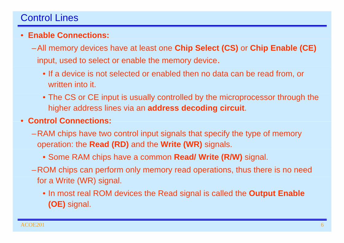
• Enable Connections:–All memory devices have at least one Chip Select (CS) or Chip Enable (CE)
input, used to select or enable the memory device.• If a device is not selected or enabled then no data can be read from, or
written into it.• The CS or CE input is usually controlled by the microprocessor through the
higher address lines via an address decoding circuit. • Control Connections:• Control Connections:
–RAM chips have two control input signals that specify the type of memory operation: the Read (RD) and the Write (WR) signals.
• Some RAM chips have a common Read/ Write (R/W) signal.–ROM chips can perform only memory read operations, thus there is no need
for a Write (WR) signal. • In most real ROM devices the Read signal is called the Output Enable
(OE) signal
ACOE201 6
(OE) signal.
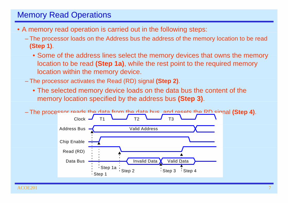
Memory Read Operations
• A memory read operation is carried out in the following steps: y p g p– The processor loads on the Address bus the address of the memory location to be read
(Step 1).• Some of the address lines select the memory devices that owns the memory• Some of the address lines select the memory devices that owns the memory
location to be read (Step 1a), while the rest point to the required memory location within the memory device.
– The processor activates the Read (RD) signal (Step 2).• The selected memory device loads on the data bus the content of the
memory location specified by the address bus (Step 3).y p y ( p )
– The processor reads the data from the data bus, and resets the RD signal (Step 4).Clock T1 T2 T3
Address Bus
Chip Enable
Valid Address
Read (RD)
Data Bus Valid DataInvalid DataStep 1a
Step 2 Step 3 Step 4
ACOE201 7
Step 1Step 2 Step 3 Step 4
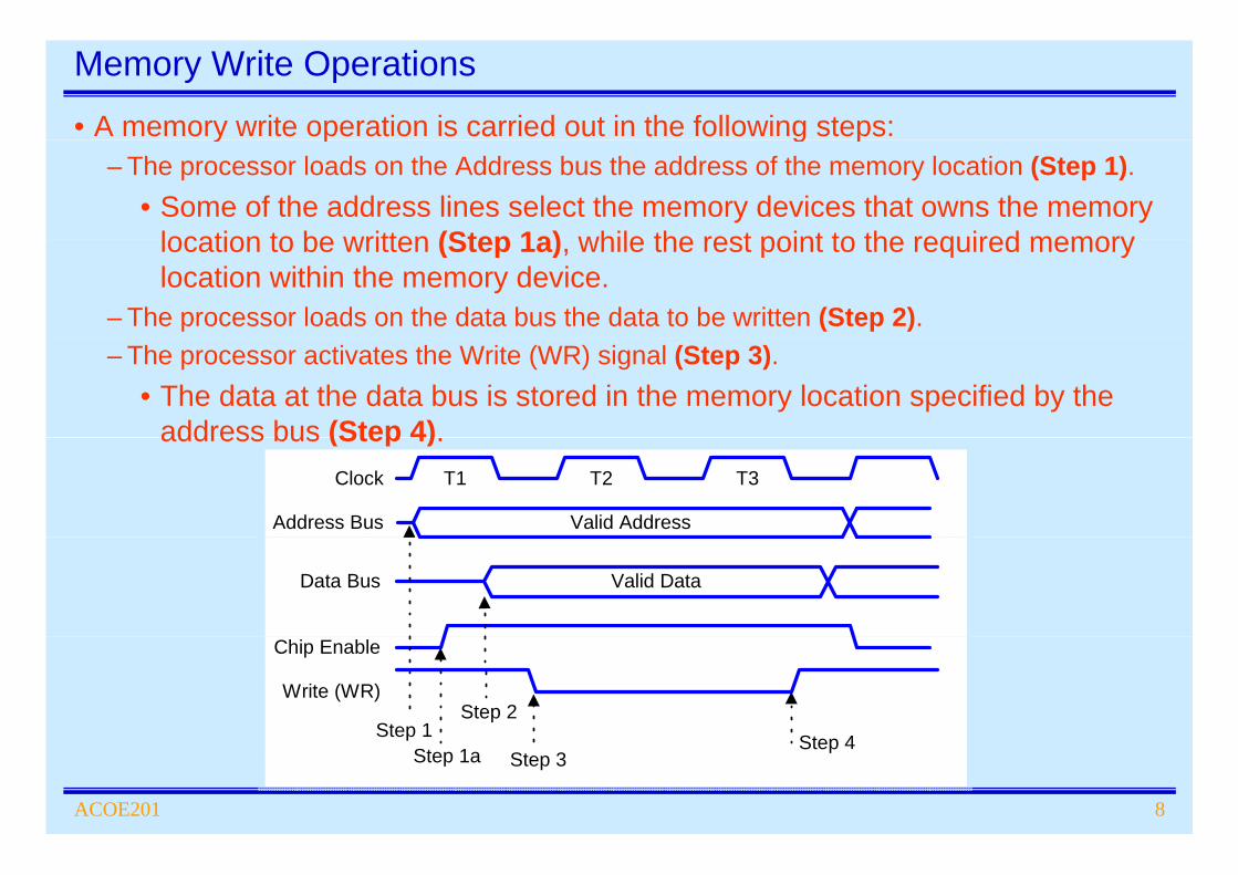
Memory Write Operations
• A memory write operation is carried out in the following steps: y p g p– The processor loads on the Address bus the address of the memory location (Step 1).
• Some of the address lines select the memory devices that owns the memory location to be written (Step 1a) while the rest point to the required memorylocation to be written (Step 1a), while the rest point to the required memory location within the memory device.
– The processor loads on the data bus the data to be written (Step 2).– The processor activates the Write (WR) signal (Step 3).
• The data at the data bus is stored in the memory location specified by the address bus (Step 4)address bus (Step 4).
Address Bus
Clock T1 T2 T3
Valid Address
Data Bus Valid Data
Chip Enable
Write (WR)
Step 1Step 2
St 4
ACOE201 8
Step 1Step 1a
Step 4Step 3
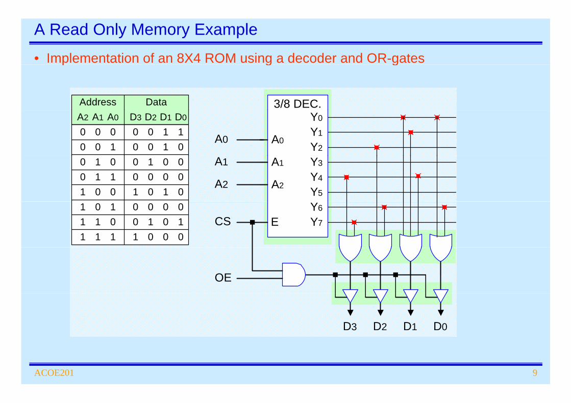
A Read Only Memory Example
• Implementation of an 8X4 ROM using a decoder and OR-gatesp g g
3/8 DEC.Address Data
Y2A0
Y0
Y1A0
A2 A1 A0 D2 D1 D0D3
0 0 0 0 1 100 0 1 0 1 00
Y3
Y4
Y5
A1
A2A2
A10 1 0 1 0 000 1 1 0 0 001 0 0 0 1 01
Y6
Y7
1 0 1 0 0 001 1 0 1 0 101 1 1 0 0 01
CS E
OE
D2 D1 D0D3
ACOE201 9
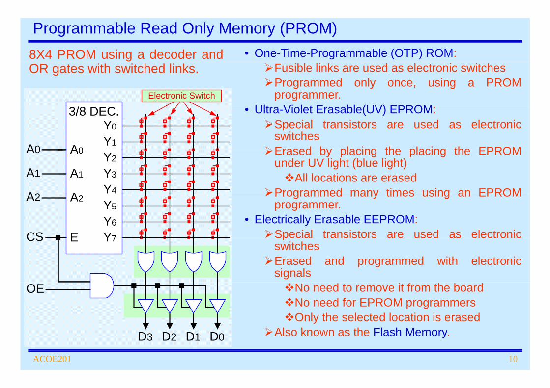
Programmable Read Only Memory (PROM)8X4 PROM using a decoder and • One-Time-Programmable (OTP) ROM:OR gates with switched links. Fusible links are used as electronic switches
Programmed only once, using a PROMprogrammer.
Ult Vi l t E bl (UV) EPROMElectronic Switch
• Ultra-Violet Erasable(UV) EPROM:Special transistors are used as electronicswitchesErased by placing the placing the EPROMA0
Y0
Y1
3/8 DEC.
A0 Erased by placing the placing the EPROMunder UV light (blue light)
All locations are erasedProgrammed many times using an EPROM
Y2A0
Y3
Y4
A1
AA2
A1
A0
Programmed many times using an EPROMprogrammer.
• Electrically Erasable EEPROM:Special transistors are used as electronic
Y6
Y5
Y7
A2
E
A2
CS Spec a t a s sto s a e used as e ect o cswitchesErased and programmed with electronicsignals
Y7ECS
No need to remove it from the boardNo need for EPROM programmersOnly the selected location is erased
OE
ACOE201 10
Also known as the Flash Memory.D2 D1 D0D3

ROM Design HomeworkROM devices are usually used in digital systems as look-up tables. Some examples y g y p pare the following exercises:
1. Design a 2-bit full adder that will produce at its output the sum of the two 2-bit numbers (A3A2) and (A1A0) that is (D3D2D1D0) = (A3A2) + (A1A0)(A3A2) and (A1A0), that is, (D3D2D1D0) (A3A2) (A1A0).
2. Design a 2-bit multiplier that will produce at its output the product of the two 2-bit numbers (A3A2) and (A1A0), that is, (D3D2D1D0) = (A3A2) * (A1A0).
3 Design a 3 bit bar graph decoder This is circuit that has as input a 3 bit binary number3. Design a 3-bit bar-graph decoder. This is circuit that has as input a 3-bit binary number and generates a code that switches ON or OFF eight LEDs as shown in figure (a) below.
4. Eight LEDs are placed on a board in a circular form. Design a circuits that will switch ON t f th LED t ti i h t i th i i th t th LEDtwo of the LEDs at a time in such a way to give the impression that the LEDs are rotating. Assume that the speed of rotation is controlled by a 0.25Hz timer.
000 001
010
011
100
101
110
111
(b)
Repeat questions 3 and 4 in software
ACOE201 11
0 0 0 0 1 1 1 1
(a) using arrays as look-up tables

RAM Cells
Static RAM (SRAM): Dynamic RAM (DRAM):( )• The basic element of a static RAM
cell is the D-Latch.D t i t d i th ll til it
y ( )• DRAM stores data in the form of
electric charges in capacitors.Ch l k t th d t• Data remains stored in the cell until it
is intentionally modified.• SRAM is fast (Access time: 1ns).
• Charges leak out, thus need to refresh data every few ms.
• DRAM is slow (Access time: 60ns).( )• SRAM needs more space on the
semiconductor chip than DRAM.SRAM i th DRAM
( )• DRAM needs less space on the
semiconductor chip than SRAM.DRAM l i th SRAM• SRAM more expensive than DRAM
• SRAM consumes power always.• SRAM is used as a Cache
• DRAM less expensive than SRAM• DRAM consumes power only when
accessed.SRAM is used as a Cache• DRAM is used as the main memory
Bit Select
Bit SelectD Q
En
Data In Data Out
W it
Bit Select
Data OutData In
ACOE201 12
EnRAM Cell
WriteDRAM Cell

Static RAM – Bit Slice
• A number of Ram Cells can be connected SelectWordSelect
together to form a column of memory cells, called a bit slice RAM.
• The Word Select signal specifies the row to
0
D Q
• The Word Select signal specifies the row to be used.
• The Bit Select signal activates the whole
EnRAM Cell
column (bit slice).• The Write Enable signal copies the bit value
at the Data In line to the RAM Cell selected
SelectWordSelect2n -1
D Qat the Data In line to the RAM Cell selected through the Word Select signal. This is true only if the Bit Select signal is activated.Th R d E bl i l i th bit l
D Q
EnRAM Cell
• The Read Enable signal copies the bit value of the RAM Cell selected through the Word Select signal to the Data Out line. This is Data
Intrue only if the Bit Select signal is activated.
• The Write Enable, Read Enable and Bit Select signal is active low (Enabled when 0). Write Enable
WriteLogic Bit
SelectLogic Read
Logic
ACOE201 13
Select signal is active low (Enabled when 0).Bit Select Data Out
Read Enable

Static RAM using bit slices (16X4 RAM)
R0A3 A Y0R0 R0 R0
RAM CellR1
A0
A1
A2
A3
er
ABCD
Y0
Y1
Y2RAM Cell
R1RAM Cell
R1RAM Cell
R1
RAM CellR216
Dec
ode
RAM CellR2
RAM CellR2
RAM CellR2
Rn
4 to
Y15Rn Rn Rn
RAM Cell RAM Cell RAM Cell RAM Cell
DIN3DIN2DIN1DIN0
Din WR CS DoutRD Din WR CS DoutRD Din WR CS DoutRD Din WR CS DoutRD
DOUT3DOUT2
WRRDCS
ACOE201 14
DOUT1DOUT0

Static RAM Chips using RAM Bit Slices
16X4 RAM using four 16X1 bit slices and one decoder (page 14)g (p g )• A SRAM chip can be constructed by using a number of RAM bit slices.• The Word Select signals are connected on the outputs of a decoder.• The Bit Select lines are connected together on a Chip Select line.• The Read Enable and Write Enable lines are connected on the RD and WR
lines respectively.lines respectively. • The disadvantage of this circuit is that for normal sized RAM chips (few Kbytes
up to Mbytes) the decoder must have thousands of outputs, hence thousands of t ( AND t f h t t)gates (one AND gate for each output).
• This disadvantage can be avoided by using the Coincident Selection.– Use one decoder to select a row, and another to select a column (a group of , ( g p
columns)– The circuit on the next page shows how a 32X2 RAM can be implemented using four
16X1 bit slices.16X1 bit slices.– Note that instead of a 5X32 decoder (with 32 output AND gates) a 4X16 and a 1X2
decoders are used (with 16 and 2 output AND gates respectively)For a 64 Kbyte RAM organized as a 1K row X 64 column matrix the number of
ACOE201 15
– For a 64 Kbyte RAM organized as a 1K-row X 64-column matrix the number of decoder AND gates is reduced from 65535 to 1088 (ie 1024+64). ..see page 16
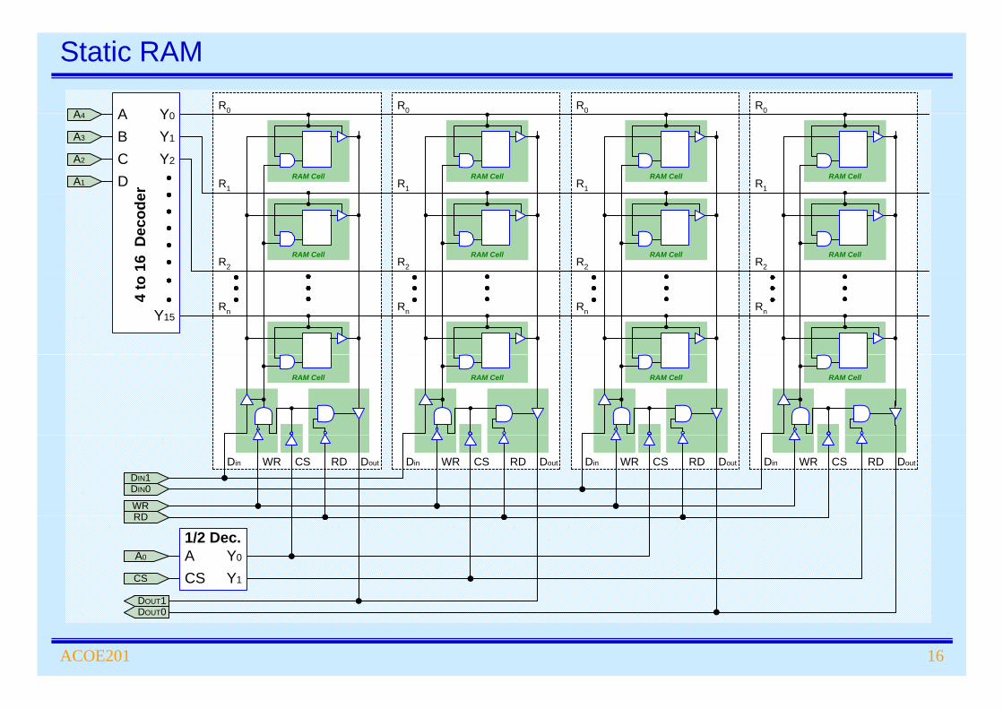
Static RAM
A4R0A Y0
R0 R0 R0A4
A1
A2
A3
RAM CellR1er
ABCD
Y0
Y1
Y2RAM Cell
R1RAM Cell
R1RAM Cell
R1
RAM CellR216
Dec
ode
RAM CellR2
RAM CellR2
RAM CellR2
Rn
4 to
Y15Rn Rn Rn
RAM Cell RAM Cell RAM Cell RAM Cell
DIN1DIN0
WRRD
Din WR CS DoutRD Din WR CS DoutRD Din WR CS DoutRD Din WR CS DoutRD
RD
CS
A0 ACS
Y0
Y1
1/2 Dec.
ACOE201 16
DOUT1DOUT0

64Kbyte Static RAM using (a) 64Kbit slices and (b) 1Kbit slices
R R RRA0
A2
A1
Dec
oder
Y0
Y1
R0
R1
RAM Cell
R0
R1
RAM Cell
R0
R1
RAM Cell
A0
A2
A1
6 D
ecod
erY0
Y1
R0
R1
RAM Cell
A9 10 to
102
3 1
RAM Cell
1
RAM Cell
1
RAM Cell
A15
16 to
655
36
1
RAM Cell
Y1023Rn
RAM Cell
Rn
RAM Cell
Rn
RAM Cell
Y65535Rn
RAM Cell
in
WR S ou
t
D in
WR S ou
t
D in
WR S ou
t
Din
WR S ou
t
D
Din(7:0)
WRRD
Di
W CS
Do
RD Di
W CS
Do
RD Di
W CS
Do
RD
A10 c. Y0
WR
Di
W CS
Do
RD
Din(7:0)
A10
6 to
64
Dec
Y0
Y1
Y63
A11
CS
A15
RD
Dout(7:0)
CS
ACOE201 17
Dout(7:0)(b)(a)
Semiconductor Memory Expansion
• The size of memory devices is usually less than the memory requirements of ay y y qcomputer system.
• In all computers, more than one memory devices are combined together to formthe main memory of the system.
–Any computer must have at least one ROM chip and one RAM chip.
• Word size memory expansion:
–Most memory devices have a word size (number of data lines) of 8 or 16 bits.
–The word size of today’s microprocessors is 32 bits (80386, 80486) or 64 bits(Pentium)
• Address size memory expansion:
–The size of common memory chips is usually less or in the order of 1M-byte.
–Most personal computers have more than 256 Mbytes of RAM.
–Workstations and other high throughput computers have more than 1Gbytes ofRAM
ACOE201 18
RAM.
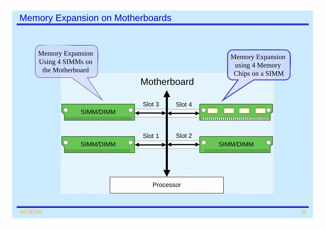
Memory Expansion on Motherboards
Memory Expansion Memory Expansion Using 4 SIMMs on
Motherboard
using 4 Memory Chips on a SIMM
Using 4 SIMMs on the Motherboard
Slot 3SIMM/DIMM
Slot 4
Slot 1 Slot 2SIMM/DIMM SIMM/DIMM
Processor
ACOE201 19
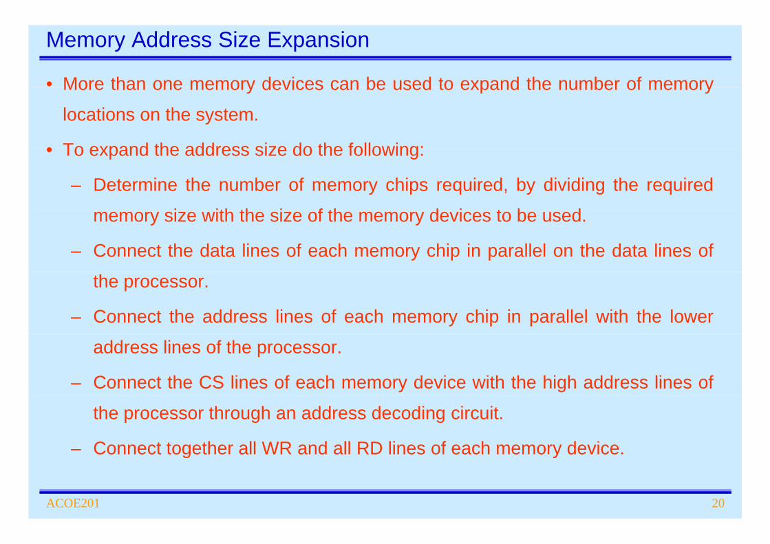
Memory Address Size Expansion
• More than one memory devices can be used to expand the number of memoryMore than one memory devices can be used to expand the number of memory
locations on the system.
• To expand the address size do the following:• To expand the address size do the following:
– Determine the number of memory chips required, by dividing the required
i ith th i f th d i t b dmemory size with the size of the memory devices to be used.
– Connect the data lines of each memory chip in parallel on the data lines of
the processor.
– Connect the address lines of each memory chip in parallel with the lower
address lines of the processor.
– Connect the CS lines of each memory device with the high address lines of
the processor through an address decoding circuit.
– Connect together all WR and all RD lines of each memory device.
ACOE201 20
g y

Address Size Expansion: (32X4 RAM module using 8X4 RAM chips)
D0
D3D2D1
Examples:M[0Ch] ← 6hM[03h] 9hD3
1
2
0
8X4RAM
D2 D1 D0 D3
1
2
0
8X4RAM
D2 D1 D0 D3
1
2
0
8X4RAM
D2 D1 D0 D3
1
2
0
8X4RAM
D2 D1 D0 M[03h] ← 9hM[1Ah] ← 3hM[14h] ← 2h
A0
A1
A2
2
3
4
5
6
A0
A1
A2
2
3
4
5
6
A0
A1
A2
2
3
4
5
6
A0
A1
A2
2
3
4
5
6
M[08h] ← 5hM[00h] ← 1hM[0Fh] ← 0h
RD
RD WR CS
6
7
RD WR CS
6
7
RD WR CS
6
7
RD WR CS
6
7
M[0Fh] ← 0hM[10h] ← AhM[18h] ← 4h
RDWR
A0A1A2
2X4 DEC
M[07h] ← 8hM[1Fh] ← EhM[17h] ← 7h
A3
A4
A5
A6
AB
Y0
Y1
Y2
Y3CS
2X4 DEC. [ ]
ACOE201 21
A6
A7 Address Selection
Y3CS
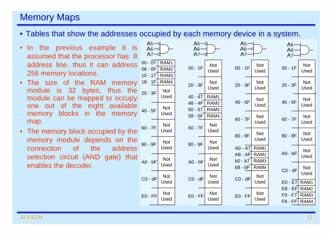
• Tables that show the addresses occupied by each memory device in a system.
Memory Maps
p y y y
• In the previous example it isassumed that the processor has 8address line thus it can address
A5
RAM100 - 07
A6A7
A5A6A7
N t
A5A6A7
N t
A5A6A7
N taddress line, thus it can address256 memory locations.
• The size of the RAM memorymodule is 32 bytes thus the
RAM1RAM2RAM3RAM4
00 07
Not
08 - 0F10 - 1718 - 1F Not
Used
NotUsed
20 - 3F
00 - 1F
NotUsed20 - 3F
NotUsed00 - 1F
NotUsed
NotUsed
20 - 3F
00 - 1F
module is 32 bytes, thus themodule can be mapped to occupyone out of the eight availablememory blocks in the memory
NotUsed
NotUsed
20 - 3F
40 - 5F
RAM1RAM2RAM3RAM4
40 - 4748 - 4F50 - 5758 - 5F
NotUsed
Not
40 - 5F
60 7F Not60 7F
40 - 5F NotUsed
map.• The memory block occupied by the
memory module depends on the
NotUsed60 - 7F
80 9F Not
NotUsed
58 5
60 - 7F
80 9F Not
NotUsed60 - 7F
80 - 9F NotUsed
NotUsed60 - 7F
80 - 9F NotUsed
connection of the addressselection circuit (AND gate) thatenables the decoder.
NotUsed
80 - 9F
A0 - bF
Used
NotUsed
80 - 9F
A0 - bF
Used RAM1RAM2RAM3RAM4
A0 - A7A8 - AFb0 - b7b8 - bF
NotUsed
Not
A0 - bF
C0 - dFNot
UsedC0 - dF
E0 - FF NotU d
NotUsedC0 - dF
E0 - FF NotU d
NotUsedC0 - dF
E0 - FF NotU d
RAM1RAM2RAM3
E0 - E7E8 - EFF0 - F7
UsedC0 - dF
ACOE201 22
E0 FF Used E0 FF Used E0 FF Used RAM4F8 - FF
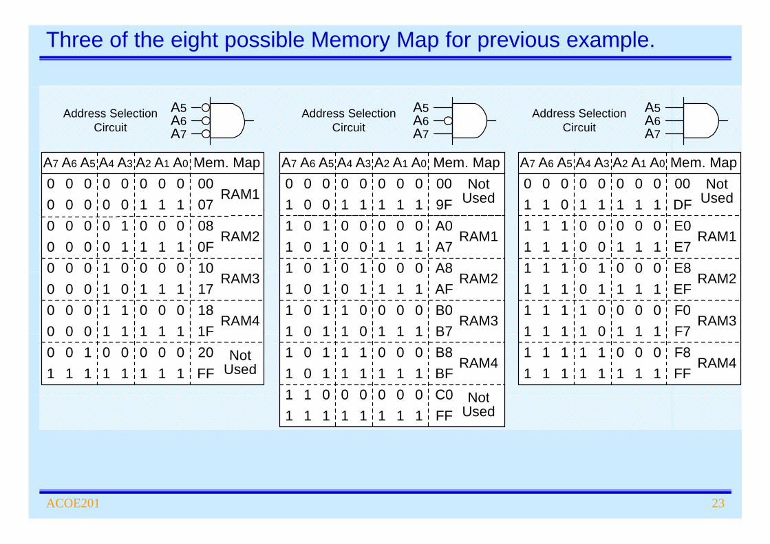
Three of the eight possible Memory Map for previous example.
Address SelectionCircuit
A5A6A7
A5A6Address Selection
Circuit A7
Address SelectionCircuit
A5A6A7
A6 A5 A4 A3 A2 A1 A0
0 0 0 0 0 0 00 0 0 0
0007
RAM1
Mem. Map
1 1 1
A7
00
A6 A5 A4 A3 A2 A1 A0 Mem. Map0 0 0 0 0 0 00 0 1 1
009F1 1 1
NotUsed
A7
01
A6 A5 A4 A3 A2 A1 A0 Mem. Map0 0 0 0 0 0 01 0 1 1
00DF1 1 1
NotUsed
A7
01
080F
RAM2
10
0 0 0 1 0 0 00 0 0 1 1 1 10 0 1 0 0 0 0
000
0 1 0 0 0 0 00 1 0 0
A0A7A8
RAM11 1 1
0 1 0 1 0 0 0
111
1 1 0 0 0 0 01 1 0 0
E0E7E8
RAM11 1 1
1 1 0 1 0 0 0
11110
17181F
RAM3
RAM4
0 0 1 0 0 0 00 0 1 0 1 1 10 0 1 1 0 0 00 0 1 1 1 1 1
0000
A8AF
RAM2
B0B7
RAM3
0 1 0 1 0 0 00 1 0 1 1 1 10 1 1 0 0 0 00 1 1 0 1 1 1
1111
E8EF
RAM2
F0F7
RAM3
1 1 0 1 0 0 01 1 0 1 1 1 11 1 1 0 0 0 01 1 1 0 1 1 1
11111F
20FF
NotUsed
0 0 1 1 1 1 10 1 0 0 0 0 01 1 1 1 1 1 1
001
B7B8BF
RAM4
C0 Not
0 1 1 0 1 1 10 1 1 1 0 0 00 1 1 1 1 1 11 0 0 0 0 0 0
1111
F7F8FF
RAM4
1 1 1 0 1 1 11 1 1 1 0 0 01 1 1 1 1 1 1
111
C0FF
NotUsed
1 0 0 0 0 0 01 1 1 1 1 1 1
11
ACOE201 23
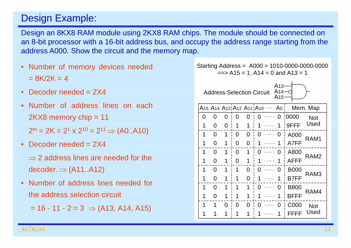
Design Example:Design an 8KX8 RAM module using 2KX8 RAM chips. The module should be connected on
8 bit ith 16 bit dd b d th dd t ti f th
• Number of memory devices needed
an 8-bit processor with a 16-bit address bus, and occupy the address range starting from the address A000. Show the circuit and the memory map.
Starting Address = A000 = 1010-0000-0000-0000Number of memory devices needed= 8K/2K = 4
• Decoder needed = 2X4A13A14Address Selection CircuitA15
Starting Address A000 1010 0000 0000 0000==> A15 = 1, A14 = 0 and A13 = 1
• Number of address lines on each2KX8 memory chip = 11
A14 A13 A0 Mem. Map0 0 0 0 0 0 0000
9FFFNot
Used
A15
0
A15
A12 A11 A10
0 0 1 1 1 112m = 2K = 21 x 210 = 211⇒ (A0..A10)
• Decoder needed = 2X4A000A7FFA800
RAM1
9FFF Used0 0 1 1 1 110 1 0 0 0 010 1 0 0 1 110 1 0 1 0 01
⇒ 2 address lines are needed for the decoder.⇒ (A11..A12)
N b f dd li d d f
A800AFFF
RAM2
B000B7FF
RAM3
0 1 0 1 0 010 1 0 1 1 110 1 1 0 0 010 1 1 0 1 11
• Number of address lines needed forthe address selection circuit
= 16 - 11 - 2 = 3 ⇒ (A13 A14 A15)
B7FFB800BFFF
RAM4
C000 Not
0 1 1 0 1 110 1 1 1 0 010 1 1 1 1 111 0 0 0 0 01
ACOE201 24
= 16 - 11 - 2 = 3 ⇒ (A13, A14, A15)FFFF Used1 1 1 1 1 11
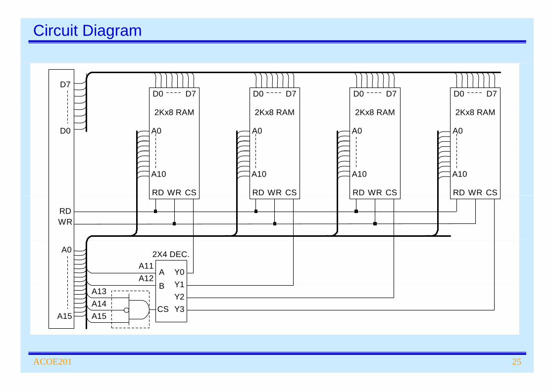
Circuit Diagram
D0 D7 D0 D7 D0 D7 D0 D7D7
A0 A0 A0 A0D0
2Kx8 RAM2Kx8 RAM2Kx8 RAM2Kx8 RAM
RD WR CS RD WR CS RD WR CS
A10
RD WR CS
A10A10A10
RDWR
A11A
B
Y0Y1
2X4 DEC.
A12
A0
B Y1Y2Y3CS
A15
A13A14A15
ACOE201 25
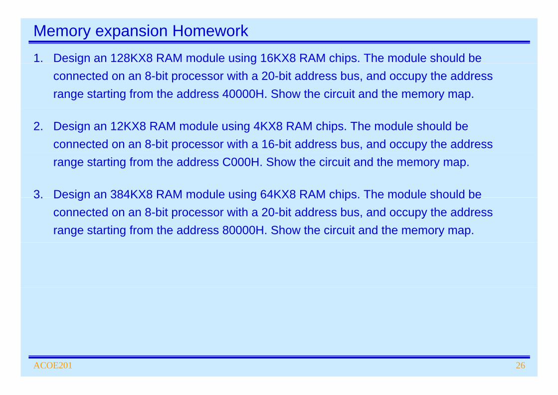
Memory expansion Homework1. Design an 128KX8 RAM module using 16KX8 RAM chips. The module should be g g p
connected on an 8-bit processor with a 20-bit address bus, and occupy the address range starting from the address 40000H. Show the circuit and the memory map.
2. Design an 12KX8 RAM module using 4KX8 RAM chips. The module should be connected on an 8-bit processor with a 16-bit address bus, and occupy the address range starting from the address C000H. Show the circuit and the memory map.
3. Design an 384KX8 RAM module using 64KX8 RAM chips. The module should be3. Design an 384KX8 RAM module using 64KX8 RAM chips. The module should be connected on an 8-bit processor with a 20-bit address bus, and occupy the address range starting from the address 80000H. Show the circuit and the memory map.
ACOE201 26