metallicnanoparticlemanipulationusing...
TRANSCRIPT
METALLIC NANOPARTICLE MANIPULATION USINGOPTOELECTRONIC TWEEZERS
Arash Jamshidi, Hsan-Yin Hsu, Justin K Valley, Aaron T Ohta, Steven Neale, and Ming C. WuBerkeley Sensor & Actuator Center (BSAC) and Department of Electrical Engineering and
Computer Sciences, University of California, Berkeley, California 94720, USA
ABSTRACTWe report on trapping of single and multiple
spherical gold nanoparticles with 60 to 250 nm diametersusing optoelectronic tweezers (OET). Thanks to the lowoptical intensities required for stable trapping (20 ptWover 1.7 ptm spot), we estimate the temperature increase inOET-trapped nanoparticles due to absorption to be AT <0.1 0C, making OET-trapped nanoparticles suitable forbiological imaging and sensing applications. In addition,we observe translational velocities of 68 rtm/s anddemonstrate trapping of both single and multiplenanoparticles in a single trap.
INTRODUCTIONIn recent years, there has been much interest in
metallic nanoparticles as biological nano-sensors due totheir interesting optical properties [1]. However, apersistent challenge has been to find techniques forinteraction with and manipulation of these nanoparticles.Optical tweezers have been used previously to trapmetallic nanoparticles of different sizes [2, 3]; however,the high optical power intensities required for stabletrapping (- 107 W/cm2) result in excessive heating inmetallic nanoparticles (AT > 550C) [4], hampering theapplication of optical tweezer-trapped particles inbiological environments. Dielectrophoresis (DEP) cantrap nanoparticles using fixed electrodes [5]; however,since the trapping positions are lithographically defined,fixed-electrode DEP lacks the capability to dynamicallyscan and manipulate the trapped particles. Trapping ofsingle molecules has also been achieved using an Anti-Brownian Electrokinetic (ABEL) trap [6] which providesextensive information about the particle dynamics.However, this technique requires the molecules to befluorescent.
In contrast, OET is an optical manipulation techniquecapable of dynamically manipulating a large number ofmicro and nanoparticles or cells over large areas usingoptical intensities 5 orders of magnitude smaller thanoptical tweezers [7]. Previously, the smallest particles thatOET could trap were limited to nanowires of diametersbelow 100 nm and approximately 5 tm length [8]. In thispaper, we report, for the first time, trapping of metallicspherical nanoparticles with 60 to 250 nm diameter usingoptoelectronic tweezers (OET).
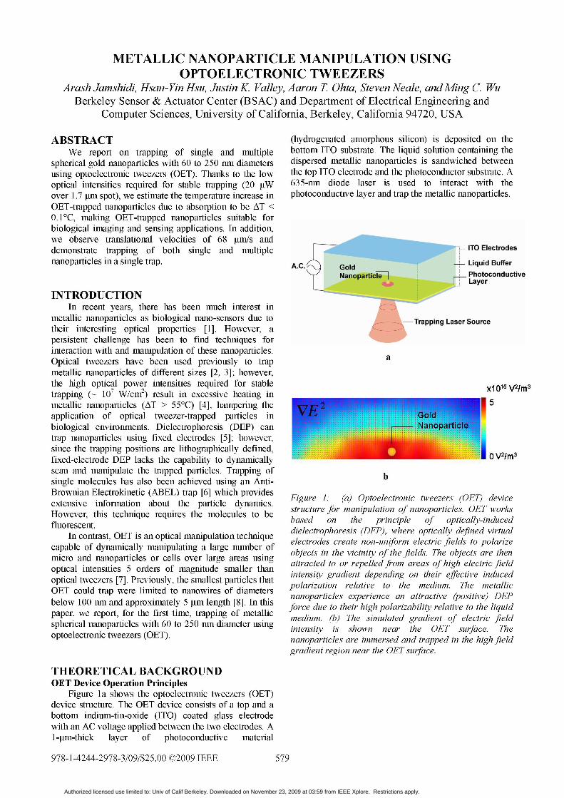
(hydrogenated amorphous silicon) is deposited on thebottom ITO substrate. The liquid solution containing thedispersed metallic nanoparticles is sandwiched betweenthe top ITO electrode and the photoconductor substrate. A635-nm diode laser is used to interact with thephotoconductive layer and trap the metallic nanoparticles.
A.C eld1lllllllllll lllllllllllllllllllllllllllllllllllllLiquid BuffNaMnopa iXle Photoconductive
...................
................... ... .................... ............................ .......
Trapping Laser Source
................................ .............
a
X1 Q16 V1m3
b
Figure 1. (a) Optoelectronic tweezers (QET) devicestructure for manipulation of nanoparticles. QET worksbased on the principle of optically-induceddielectrophoresis (DEP), where optically defined virtualelectrodes create non-uniform electric fields to polarizeobjects in the vicinity of the fields. The objects are thenattracted to or repelledfrom areas of high electric fieldintensity gradient depending on their effective inducedpolarization relative to the medium. The metallicnanoparticles experience an attractive (positive) DEPforce due to their high polarizability relative to the liquidmedium. (b) The simulated gradient of electric fieldintensity is shown near the QET surface. Thenanoparticles are immersed and trapped in the high fieldgradient region near the QETsurface.
THEORETICAL BACKGROUNDOET Device Operation Principles
Figure la shows the optoelectronic tweezers (OET)device structure. The OET device consists of a top and abottom indium-tin-oxide (ITO) coated glass electrodewith an AC voltage applied between the two electrodes. A1-pim-thick layer of photoconductive material
978-1-4244-2978-3/09/$25.00 ©2009 IEEE 579
Authorized licensed use limited to: Univ of Calif Berkeley. Downloaded on November 23, 2009 at 03:59 from IEEE Xplore. Restrictions apply.
When there is no laser light present, the impedance ofthe photoconductive layer is higher than that of the liquidlayer and the majority of the applied AC voltage isdropped across the photoconductive layer. However,once the laser light is introduced, it generates electron-hole pairs in the photoconductive layer, reducing theimpedance of the photoconductor layer below that of theliquid layer. Therefore, the majority of voltage is switchedfrom the photoconductive layer to the liquid layer in thearea that laser is present. Since the voltage switch occursonly in the area that laser source is present, the electricfield in the liquid will have a non-uniform profile. Thisnon-uniform field polarizes the metallic nanoparticles inits vicinity, attracting them to areas of high electric fieldintensity gradient according to the DEP force principle.
Figure lb shows the finite-element simulation of thegradient of the non-uniform electric field intensity for anapplied bias of 20 Vpp at 100 kHz.
Dielectrophoresis ForceThe non-uniform electric field present in the liquid
layer induces a dipole moment (p) in the metallicnanoparticles. The induced dipole interacts with theelectric field, resulting in a dielectrophoreticforce, F = (p V)E, which attracts the nanoparticles toareas of highest field intensity gradient [9].
The DEP force expression for a spherical particle isgiven by [9]:
FDEP = 2zr 3 m Re{K}V(E 2) (1)
where, r is the radius of the particle, £m is the permittivityof the liquid medium, Re{K} is the real part of theClausius-Mossotti (CM) factor given by,Re{K}= Re{(£p-4 )/(£p + 24 )}J, where
= - j cl/o, with p and m subscripts referring to theparticle and the liquid medium, respectively.
As shown in Figure lb, the gradient of field intensityis strongest near the OET surface and falls off sharply aswe move away from the surface. Due to the nanoparticlessmall size, they are immersed in the high-VE2 regionnear the OET surface. The gradient of field intensity canbe simulated using COMSOL finite-element modelingand is estimated to be 1016 - 1017 V2/m3 near the OETsurface. Using this value, we can estimate the strength ofthe DEP force for a 100 nm diameter nanoparticle to beapproximately 0.1 pN.
To estimate the velocity of the nanoparticles due tothis DEP force, we can use the drag force acting on thespherical nanoparticles [10],
F = 6J7Urvdrag
Temperature AnalysisUsing a similar analysis to ref. [4], we can estimate
the temperature increase in the OET-trapped nanoparticlesas AT = Pabs /(4m-C), where C is the thermalconductivity of water (0.6 W/K.m), r is the radial distancefrom the nanoparticle's center, and Pabs is the absorbedpower in the nanoparticle given by abs = cbabsI2 where I
is the laser intensity and acabs is the absorption crosssection of the nanoparticle given byCabs = (2z1m / Al) X Im[3V(6 4- )/(£, + 24m )], where
8, ~1.77 (nm - 1.33) and £p ~-10.66+il.37 at i635 nm and V is the volume of the nanoparticle. For a 20ptW trapping laser source with 1.7 ptm (FWHM) spot size,we estimate the temperature increase at the surface of 60to 250 nm diameter gold nanoparticles due to absorptionto be less than 0.1°C.
It is important to note that this calculation does nottake into account the temperature increase due to the jouleheating in the liquid layer. The joule heating effect can beroughly estimated as [11]: ATjovIe = 0liquid V2 /(2C),where aliquid is the liquid conductivity, V is the appliedvoltage, and C is the thermal conductivity of water. Usingthe typical experimental values for nanoparticle trapping(aiquid = 1-10 mS/m, V= 10-20 Vpp), we can estimatethe temperature increase due to joule heating to be oforders of a few 'C which is about an order of magnitudelarger than the temperature increase due to absorption inmetallic nanoparticles. Therefore, joule heating would bethe dominant effect in calculating the total temperatureincrease in the trapping environment.
EXPERIMENTAL RESULTSExperimental Setup
Figure 2 shows the experimental setup used for themetallic nanoparticle manipulation using OET. Goldnanoparticles with 60 to 250 nm diameters with anapproximately 1010 particles/ml density were diluted in a2.6 mS/m conductivity solution of DI water and KCl. 4ptL of the sample was introduced into the OET device.Majority of the nanoparticles showed strong Brownianwhile a portion of the particles adhered to the surface. A635 nm diode laser with 20 ptW power and 1.7 tm(FWHM) optical spot size at the OET surface was used totrap the nanoparticles. AC voltages of 10-20 Vpp at 50-100 kHz frequency were applied to the OET device. Darkfield microscopy using a BX51M Olympus microscopewas used to visualize the nanoparticles and images werecaptured using a CCD camera.
(2)
where, r is the particle's radius, q is dynamic viscosity ofwater, and vDrag is the drag velocity. Equating this force tothe DEP force (FDEP = FDrag), we can achieve vDrag closeto 100 rim/s.
580
Authorized licensed use limited to: Univ of Calif Berkeley. Downloaded on November 23, 2009 at 03:59 from IEEE Xplore. Restrictions apply.

applied AC voltage. The experimental data follows aquadratic trend (black fitted line) which is expected sincethe DEP force is proportional to the gradient of the fieldintensity.
A 68 rtm/s maximum translation speed is measuredfor an applied AC voltage of 20 Vpp. This measuredtranslational speed is close to the calculated speeds formetallic nanoparticles. In addition, a maximum trappingradius of approximately 28 ptm is measured at 20 Vpp.
OET Device_mmmmmoommummo~~ XYZ Stage 80
50150 Beam
Spliter
Figure 2: Experimental setup for manipulation ofmetallicnanoparticles. A 10-m W, 635nm diode laser was expanded5 x, attenuated to 20 W, andfocused onto the OET chipwith 1.7 uim (FWHM) using a 20 x objective lens. Thenanoparticles were visualized using darkfield microscopyand a CCD camera.
DEP Manipulation of Metallic NanoparticlesFigure 3 shows trapping of a single 100 nm gold
nanoparticle using OET. The nanoparticle experiences a
positive DEP force and is attracted to the laser trappingsource. By manually adjusting the laser trap position, thenanoparticle is transported over an approximately 200
2
~tM area in 12 seconds.
Figure 3: Trapping and transport process of a single 100nm gold nanoparticle using OET The nanoparticle istransported over an approximately 200 tUm2 area in 12seconds.
E
0)
0.
,)
0
-W
._
e-
60 [
40 F
20 F
0
0 5 10 15Peak-to-peak AC Voltage (V)
20
Figure 4: OET-trapped nanoparticles' translational speedas a function of the applied voltage. A maximumtranslational speed of 68 tumls at 20 Vpp is achieved. Theexperimental data follows a quadratic trend (black fittedcurve). This is expected since the DEP force isproportional to VE2.
When more than one nanoparticle is trapped in thelaser, the particles experience a mutual repulsive forcedue to two effects. First, nanoparticles carry a negativesurface charge with a zeta potential of S = -70 mVresulting in a mutual columbic repulsion. Second, thedipoles induced in the nanoparticles interact with eachother resulting in a dipole-dipole repulsive force which isa function of the applied voltage. By measuring thetranslation speeds of the particles after removing the lasertrap, we can calculate the net repulsive force between two100 nm gold nanoparticles to be approximately 23 fN at20 Vpp (Figure 5a).
We can also observe this repulsive force acting on
more than two particles as shown in Figure 5b for threenanoparticles. In the beginning the three particles are
trapped in the laser source (filtered out), once the lasertrap is removed, the mutual repulsion between theparticles repels them from each other.
Trap CharacterizationTo quantify the maximum trapping speed of the
metallic gold nanoparticles, we used an ESP-300 Newportmotorized actuator controller and a LTA-HL motorizedactuator to move the microscope stage relative to theoptical pattern. Figure 4 shows the maximum translationalspeeds of 100 nm gold nanoparticles as a function of the
581
In r?=0
tDr-- -
II
Authorized licensed use limited to: Univ of Calif Berkeley. Downloaded on November 23, 2009 at 03:59 from IEEE Xplore. Restrictions apply.

a
207
0s 150LL
X 10
0.
5
00 5 10 15
Peak-to-Peak AC Voltage (V)
h
Figure 5: (a) The repulsive force (Frep) between twonanoparticles (due to dipole-dipole interaction andcolumbic repulsion) as a function of applied voltage. (b)The repulsive force interaction is also observedfor threenanoparticles. In the beginning, the particles are trappedusing OET (laser filtered out), once the trap is removed,the nanoparticles repel each other.
Trapping of Multiple NanoparticlesFigure 6a-d shows trapping and transport of five 250
nm gold nanoparticles using OET. Nanoparticles areconcentrated in the OET trap and can be transported byscanning the laser trap manually, once the laser trap isremoved, nanoparticles undergo Brownian motion and thefive gold nanoparticles are distinctly observable. Theability to concentrate the nanoparticles in a single spot isimportant to enhance the sensitivity of the dynamic hot-spots for imaging and sensing applications.
concentrated in the laser trap. (b) Nanoparticles aretransported to a new location by manually adjusting thelaser position. (c) Laser trap is removed andnanoparticles undergo Brownian motion. (d) Five goldnanoparticles are distinctly observable after removal ofthe trap.
CONCLUSIONIn conclusion, we report on trapping single and
multiple spherical gold nanoparticles with 60 to 250 nmdiameters using optoelectronic tweezers. Due to lowoptical intensities required for stable trapping we estimatethe temperature increase in OET-trapped nanoparticlesdue to absorption to be AT < 0.1°C. In addition, weobserve translation speeds of 68 rtm/s for 100 nm goldnanoparticles at 20 Vpp applied voltage.
ACKNOWLEDGEMENTThis work was supported in part by the National
Institutes of Health through the NIH Roadmap forMedical Research (Grant #PN2 EY018228) and DARPA.We also thank Lawrence Berkeley National Laboratory(LBNL) Molecular Foundry and UC BerkeleyMicrofabrication Laboratory.
REFERENCES[1] Anker, J.N., et al., Nature Materials 7, pp. 442 - 453
(2008).[2] Svoboda, K. and Block, S. M. Optics Letters 19, pp.
930 - 932, (1994).[3] Hansen, P. M., et al., Nano Letters 5, pp. 2429 - 2431,
(2005).[4] Seol, Y., Carpenter, A. E., Perkins, T. T., Opt. Lett.
31, pp. 1937 - 1942, (2006).[5] Zheng, L., Li, S., Brody, J. P., Burke, P. J., Langmuir
20, pp. 8612-8619, (2004).[6] Cohen, A. E., Moemer, W. E., Optics Express 10, pp.
6941-6956, (2008).[7] Chiou, P.Y., Ohta, A. T., Wu, M. C., Nature, 436, pp.
370-372, (2005).[8] Jamshidi, A., et al., Nature Photonics 2, pp. 85 - 89,
(2008).[9] T. B. Jones, Electromechanics of Particles(Cambridge: Cambridge University Press), 1995.[10] H. Morgan and N. Green, AC Electrokinetics:colloids and nanoparticles (Research Studies Press Ltd.),2003.[11] Ramos, A., et al., J. Phys. D: Appl. Phys. 31, pp.2338 - 2353 (1998).
Figure 6: Trapping and transport offive 250 nm goldnanoparticles. (a) Nanoparticles are trapped and
582
0 ~F I
% IX
eX~ /.
Authorized licensed use limited to: Univ of Calif Berkeley. Downloaded on November 23, 2009 at 03:59 from IEEE Xplore. Restrictions apply.