methods of analysis and selected topics(dc) - … · not permit the reduction technique used in...
TRANSCRIPT

8.1 INTRODUCTION
The circuits described in the previous chapters had only one source ortwo or more sources in series or parallel present. The step-by-step pro-cedure outlined in those chapters cannot be applied if the sources arenot in series or parallel. There will be an interaction of sources that willnot permit the reduction technique used in Chapter 7 to find quantitiessuch as the total resistance and source current.
Methods of analysis have been developed that allow us to approach,in a systematic manner, a network with any number of sources in anyarrangement. Fortunately, these methods can also be applied to networkswith only one source. The methods to be discussed in detail in this chap-ter include branch-current analysis, mesh analysis, and nodal analy-sis. Each can be applied to the same network. The “best” method cannotbe defined by a set of rules but can be determined only by acquiring afirm understanding of the relative advantages of each. All the methodscan be applied to linear bilateral networks. The term linear indicates thatthe characteristics of the network elements (such as the resistors) areindependent of the voltage across or current through them. The secondterm, bilateral, refers to the fact that there is no change in the behavior orcharacteristics of an element if the current through or voltage across theelement is reversed. Of the three methods listed above, the branch-current method is the only one not restricted to bilateral devices. Beforediscussing the methods in detail, we shall consider the current sourceand conversions between voltage and current sources. At the end of thechapter we shall consider bridge networks and D-Y andY-D conversions.Chapter 9 will present the important theorems of network analysis thatcan also be employed to solve networks with more than one source.
8.2 CURRENT SOURCES
The concept of the current source was introduced in Section 2.4 withthe photograph of a commercially available unit. We must now investi-
Methods of Analysis andSelected Topics (dc)
NA8
256 METHODS OF ANALYSIS AND SELECTED TOPICS (dc)
gate its characteristics in greater detail so that we can properly deter-mine its effect on the networks to be examined in this chapter.
The current source is often referred to as the dual of the voltagesource. A battery supplies a fixed voltage, and the source current canvary; but the current source supplies a fixed current to the branch inwhich it is located, while its terminal voltage may vary as determinedby the network to which it is applied. Note from the above that dualitysimply implies an interchange of current and voltage to distinguish thecharacteristics of one source from the other.
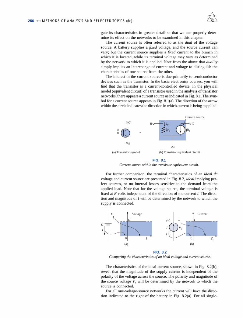
The interest in the current source is due primarily to semiconductordevices such as the transistor. In the basic electronics courses, you willfind that the transistor is a current-controlled device. In the physicalmodel (equivalent circuit) of a transistor used in the analysis of transistornetworks, there appears a current source as indicated in Fig. 8.1. The sym-bol for a current source appears in Fig. 8.1(a). The direction of the arrowwithin the circle indicates the direction in which current is being supplied.
NA
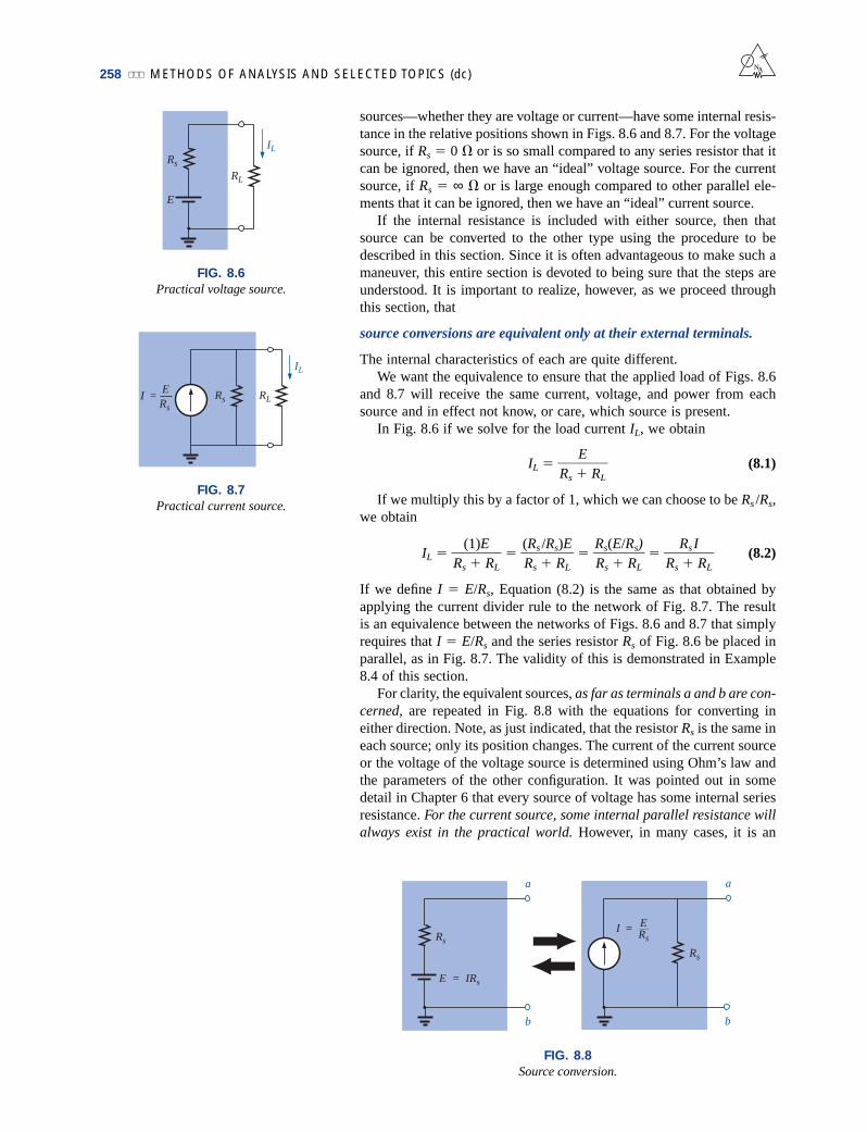
For further comparison, the terminal characteristics of an ideal dcvoltage and current source are presented in Fig. 8.2, ideal implying per-fect sources, or no internal losses sensitive to the demand from theapplied load. Note that for the voltage source, the terminal voltage isfixed at E volts independent of the direction of the current I. The direc-tion and magnitude of I will be determined by the network to which thesupply is connected.
FIG. 8.1
Current source within the transistor equivalent circuit.
(a) Transistor symbol (b) Transistor equivalent circuit
Current source
βre
C
E
B Ib
βIbB
C
E
=
FIG. 8.2
Comparing the characteristics of an ideal voltage and current source.
Voltage
EI
E
0 I
(a)
Current
Vs
I
I
0
(b)
Vs
(+) –
(–) +
I
The characteristics of the ideal current source, shown in Fig. 8.2(b),reveal that the magnitude of the supply current is independent of thepolarity of the voltage across the source. The polarity and magnitude ofthe source voltage Vs will be determined by the network to which thesource is connected.
For all one-voltage-source networks the current will have the direc-tion indicated to the right of the battery in Fig. 8.2(a). For all single-

SOURCE CONVERSIONS 257
current-source networks, it will have the polarity indicated to the rightof the current source in Fig. 8.2(b).
In review:
A current source determines the current in the branch in which it islocated
and
the magnitude and polarity of the voltage across a current source area function of the network to which it is applied.
EXAMPLE 8.1 Find the source voltage Vs and the current I1 for thecircuit of Fig. 8.3.
Solution:
I1 I 10 mA
Vs V1 I1R1 (10 mA)(20 k) 200 V
EXAMPLE 8.2 Find the voltage Vs and the currents I1 and I2 for thenetwork of Fig. 8.4.
Solution:
Vs E 12 V
I2 VR
R ER
3 A
Applying Kirchhoff’s current law:
I I1 I2
and I1 I I2 7 A 3 A 4 A
EXAMPLE 8.3 Determine the current I1 and the voltage Vs for the net-work of Fig. 8.5.
Solution: Using the current divider rule:
I1 2 A
The voltage V1 is
V1 I1R1 (2 A)(2 ) 4 V
and, applying Kirchhoff’s voltage law,
Vs V1 20 V 0
and Vs V1 20 V 4 V 20 V 24 V
Note the polarity of Vs as determined by the multisource network.
8.3 SOURCE CONVERSIONS
The current source described in the previous section is called an idealsource due to the absence of any internal resistance. In reality, all
(1 )(6 A)1 2
R2IR2 R1
12 V4
NA
–I = 10 mA
+R1 20 k
I1
Vs
–
+V1
FIG. 8.3
Example 8.1.
E R12 V 4
I1
Vs 7 A
+
–I
I2
FIG. 8.4
Example 8.2.
+ 20 V2
R1
6 A
–
+
Vs
R2
1
+ V1 –
I
I1
FIG. 8.5
Example 8.3.
258 METHODS OF ANALYSIS AND SELECTED TOPICS (dc)
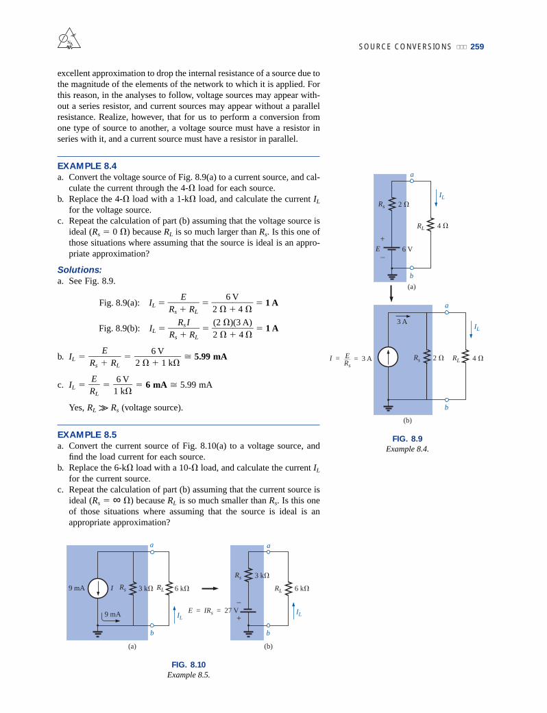
sources—whether they are voltage or current—have some internal resis-tance in the relative positions shown in Figs. 8.6 and 8.7. For the voltagesource, if Rs 0 or is so small compared to any series resistor that itcan be ignored, then we have an “ideal” voltage source. For the currentsource, if Rs ∞ or is large enough compared to other parallel ele-ments that it can be ignored, then we have an “ideal” current source.
If the internal resistance is included with either source, then thatsource can be converted to the other type using the procedure to bedescribed in this section. Since it is often advantageous to make such amaneuver, this entire section is devoted to being sure that the steps areunderstood. It is important to realize, however, as we proceed throughthis section, that
source conversions are equivalent only at their external terminals.
The internal characteristics of each are quite different.We want the equivalence to ensure that the applied load of Figs. 8.6
and 8.7 will receive the same current, voltage, and power from eachsource and in effect not know, or care, which source is present.
In Fig. 8.6 if we solve for the load current IL, we obtain
IL Rs
ERL
(8.1)
If we multiply this by a factor of 1, which we can choose to be Rs /Rs,we obtain
IL Rs
(1
)ERL
(RR
s
s
/Rs
R)E
L
RR
s
s
(
E/RR
s
L
)
Rs
R
s IRL
(8.2)
If we define I E/Rs, Equation (8.2) is the same as that obtained byapplying the current divider rule to the network of Fig. 8.7. The resultis an equivalence between the networks of Figs. 8.6 and 8.7 that simplyrequires that I E/Rs and the series resistor Rs of Fig. 8.6 be placed inparallel, as in Fig. 8.7. The validity of this is demonstrated in Example8.4 of this section.
For clarity, the equivalent sources, as far as terminals a and b are con-cerned, are repeated in Fig. 8.8 with the equations for converting ineither direction. Note, as just indicated, that the resistor Rs is the same ineach source; only its position changes. The current of the current sourceor the voltage of the voltage source is determined using Ohm’s law andthe parameters of the other configuration. It was pointed out in somedetail in Chapter 6 that every source of voltage has some internal seriesresistance. For the current source, some internal parallel resistance willalways exist in the practical world. However, in many cases, it is an
NA
Rs
RL
IL
E
RsRL
IL
E RsI =
FIG. 8.6
Practical voltage source.
FIG. 8.7
Practical current source.
a
b
a
b
E = IRs
Rs
Rs
I = ERs
FIG. 8.8
Source conversion.
SOURCE CONVERSIONS 259
excellent approximation to drop the internal resistance of a source due tothe magnitude of the elements of the network to which it is applied. Forthis reason, in the analyses to follow, voltage sources may appear with-out a series resistor, and current sources may appear without a parallelresistance. Realize, however, that for us to perform a conversion fromone type of source to another, a voltage source must have a resistor inseries with it, and a current source must have a resistor in parallel.
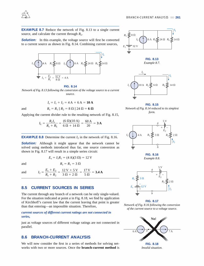
EXAMPLE 8.4
a. Convert the voltage source of Fig. 8.9(a) to a current source, and cal-culate the current through the 4- load for each source.
b. Replace the 4- load with a 1-k load, and calculate the current IL
for the voltage source.c. Repeat the calculation of part (b) assuming that the voltage source is
ideal (Rs 0 ) because RL is so much larger than Rs. Is this one ofthose situations where assuming that the source is ideal is an appro-priate approximation?
Solutions:
a. See Fig. 8.9.
Fig. 8.9(a): IL Rs
ERL
2
6
V4
1 A
Fig. 8.9(b): IL Rs
R
s IRL
2(2
)(34A
) 1 A
b. IL Rs
ERL
5.99 mA
c. IL RE
L 6 mA 5.99 mA
Yes, RL k Rs (voltage source).
EXAMPLE 8.5
a. Convert the current source of Fig. 8.10(a) to a voltage source, andfind the load current for each source.
b. Replace the 6-k load with a 10- load, and calculate the current IL
for the current source.c. Repeat the calculation of part (b) assuming that the current source is
ideal (Rs ∞ ) because RL is so much smaller than Rs. Is this oneof those situations where assuming that the source is ideal is anappropriate approximation?
6 V1 k
6 V2 1 k
NA
(a)
Rs
RL
2
–
+6 V
4
IL
E
a
b
(b)
Rs RL2 4
IL
a
b
I = = 3 AERs
3 A
FIG. 8.9
Example 8.4.
FIG. 8.10
Example 8.5.
(b)
Rs
RL
3 k
–
+
6 k
ILE = IRs = 27 V
a
b
(a)
Rs RL3 k 6 k
IL
a
b
9 mA I
9 mA

260 METHODS OF ANALYSIS AND SELECTED TOPICS (dc)
Solutions:
a. See Fig. 8.10.
Fig. 8.10(a): IL Rs
R
s IRL
3 mA
Fig. 8.10(b): IL Rs
ERL
3 mA
b. IL Rs
R
s IRL
8.97 mA
c. IL I 9 mA 8.97 mA
Yes, Rs k RL (current source).
8.4 CURRENT SOURCES IN PARALLEL
If two or more current sources are in parallel, they may all be replacedby one current source having the magnitude and direction of the resul-tant, which can be found by summing the currents in one direction andsubtracting the sum of the currents in the opposite direction. The newparallel resistance is determined by methods described in the discussionof parallel resistors in Chapter 5. Consider the following examples.
EXAMPLE 8.6 Reduce the parallel current sources of Figs. 8.11 and8.12 to a single current source.
(3 k)(9 mA)3 k 10
27 V9 k
27 V3 k 6 k
(3 k)(9 mA)3 k 6 k
NA
FIG. 8.11
Example 8.6.
FIG. 8.12
Example 8.6.
Is = 10 A – 6 A = 4 ARs = 3 6 = 2
6 AR1 3
10 AR2 6
4 AR3 2 Is
3 A R1 4 Rs 4 Is7 A 4 A 8 A
Is = 7 A + 4 A – 3 A = 8 ARs = R1 = 4
Solution: Note the solution in each figure.
BRANCH-CURRENT ANALYSIS 261
EXAMPLE 8.7 Reduce the network of Fig. 8.13 to a single currentsource, and calculate the current through RL.
Solution: In this example, the voltage source will first be convertedto a current source as shown in Fig. 8.14. Combining current sources,
NA
I2 6 A 24 R2 RL 14
IL
R1 8
E1 32 V
FIG. 8.13
Example 8.7.I1 4 A 8 R1 24 R2I2 6 A RL 14
IL
I1 =E1R1
=32 V8
= 4 A
Is I1 I2 4 A 6 A 10 A
and Rs R1 R2 8 24 6
Applying the current divider rule to the resulting network of Fig. 8.15,
IL Rs
Rs Is
RL 3 A
EXAMPLE 8.8 Determine the current I2 in the network of Fig. 8.16.
Solution: Although it might appear that the network cannot besolved using methods introduced thus far, one source conversion asshown in Fig. 8.17 will result in a simple series circuit:
Es I1R1 (4 A)(3 ) 12 V
and Rs R1 3
and I2 3.4 A
8.5 CURRENT SOURCES IN SERIES
The current through any branch of a network can be only single-valued.For the situation indicated at point a in Fig. 8.18, we find by applicationof Kirchhoff’s current law that the current leaving that point is greaterthan that entering—an impossible situation. Therefore,
current sources of different current ratings are not connected inseries,
just as voltage sources of different voltage ratings are not connected inparallel.
8.6 BRANCH-CURRENT ANALYSIS
We will now consider the first in a series of methods for solving net-works with two or more sources. Once the branch-current method is
17 V5
12 V 5 V3 2
Es E2Rs R2
60 A
20
(6 )(10 A)6 14
FIG. 8.14
Network of Fig. 8.13 following the conversion of the voltage source to a currentsource.
Is 10 A 6 Rs RL 14
IL
Is
FIG. 8.15
Network of Fig. 8.14 reduced to its simplest form.
I1 4 A 3 R1 R2 2
I2
5 Va
b
E2
–+
FIG. 8.16
Example 8.8.
E23 –+
Rs
Es 12 V
2 R2
5 V
I2+
–
a
b
FIG. 8.17
Network of Fig. 8.16 following the conversion of the current source to a voltage source.
a6 A 7 A
No!
FIG. 8.18
Invalid situation.
(a) (b)
1 2 1 2 3 1 2
3 1 2
3
262 METHODS OF ANALYSIS AND SELECTED TOPICS (dc)
mastered, there is no linear dc network for which a solution cannot befound. Keep in mind that networks with two isolated voltage sourcescannot be solved using the approach of Chapter 7. For additional evi-dence of this fact, try solving for the unknown elements of Example 8.9using the methods introduced in Chapter 7. The network of Fig. 8.21can be solved using the source conversions described in the last section,but the method to be described in this section has applications farbeyond the configuration of this network. The most direct introductionto a method of this type is to list the series of steps required for itsapplication. There are four steps, as indicated below. Before continuing,understand that this method will produce the current through eachbranch of the network, the branch current. Once this is known, all otherquantities, such as voltage or power, can be determined.
1. Assign a distinct current of arbitrary direction to each branch ofthe network.
2. Indicate the polarities for each resistor as determined by theassumed current direction.
3. Apply Kirchhoff’s voltage law around each closed, independentloop of the network.
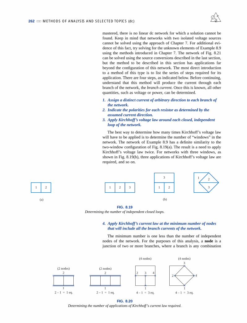
The best way to determine how many times Kirchhoff’s voltage lawwill have to be applied is to determine the number of “windows” in thenetwork. The network of Example 8.9 has a definite similarity to thetwo-window configuration of Fig. 8.19(a). The result is a need to applyKirchhoff’s voltage law twice. For networks with three windows, asshown in Fig. 8.19(b), three applications of Kirchhoff’s voltage law arerequired, and so on.
NA
4. Apply Kirchhoff’s current law at the minimum number of nodesthat will include all the branch currents of the network.
The minimum number is one less than the number of independentnodes of the network. For the purposes of this analysis, a node is ajunction of two or more branches, where a branch is any combination
FIG. 8.19
Determining the number of independent closed loops.
(4 nodes)
2
3
4
14 – 1 = 3 eq.
(4 nodes)
2 3 4
14 – 1 = 3 eq.
(2 nodes)2
12 – 1 = 1 eq.
(2 nodes)2
12 – 1 = 1 eq.
FIG. 8.20
Determining the number of applications of Kirchhoff’s current law required.
NA BRANCH-CURRENT ANALYSIS 263
4
6 V
I1
E2
–
+
1
2 VE1
–
+
2 R1
I2
I3
bd
a
c
R2
R3
FIG. 8.21
Example 8.9.Definedby I1 I2
4
6 V
–
a
+
21
I1
E2
–
+
–
+1
2 VE1
–
+
–
+2
I3
Definedby I2
Fixedpolarity
Fixedpolarity
Defined by I3
FIG. 8.22
Inserting the polarities across the resistive elements as defined by the chosenbranch currents.
Step 3: Kirchhoff’s voltage law is applied around each closed loop (1and 2) in the clockwise direction:
and
of series elements. Figure 8.20 defines the number of applications ofKirchhoff’s current law for each configuration of Fig. 8.19.
5. Solve the resulting simultaneous linear equations for assumedbranch currents.
It is assumed that the use of the determinants method to solve for thecurrents I1, I2, and I3 is understood and is a part of the student’s mathe-matical background. If not, a detailed explanation of the procedure isprovided in Appendix C. Calculators and computer software packagessuch as Mathcad can find the solutions quickly and accurately.
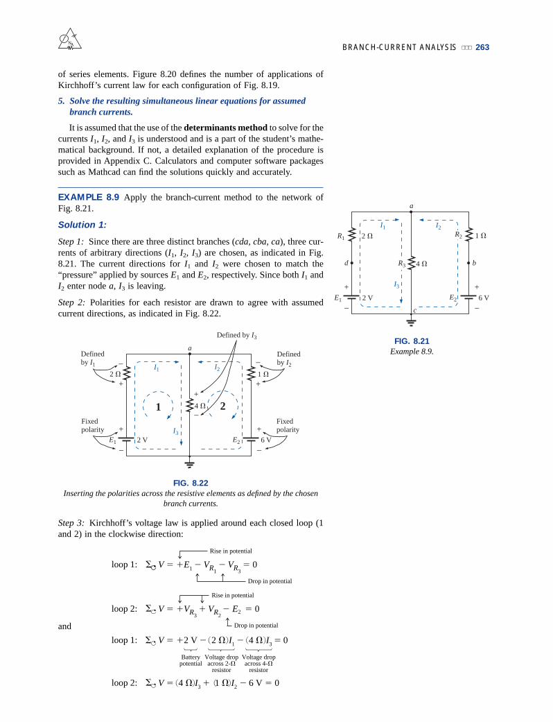
EXAMPLE 8.9 Apply the branch-current method to the network ofFig. 8.21.
Solution 1:
Step 1: Since there are three distinct branches (cda, cba, ca), three cur-rents of arbitrary directions (I1, I2, I3) are chosen, as indicated in Fig.8.21. The current directions for I1 and I2 were chosen to match the“pressure” applied by sources E1 and E2, respectively. Since both I1 andI2 enter node a, I3 is leaving.
Step 2: Polarities for each resistor are drawn to agree with assumedcurrent directions, as indicated in Fig. 8.22.
loop 1: V E1 VR1 VR3 0
Rise in potential
Drop in potential
loop 2: V VR3 VR2 E2 0
Rise in potential
Drop in potential
loop 1: V 2 V 2 I1 4 I3 0
loop 2: V 4 I3 1 I2 6 V 0
Batterypotential
Voltage dropacross 2-
resistor
Voltage dropacross 4-
resistor

264 METHODS OF ANALYSIS AND SELECTED TOPICS (dc)
Step 4: Applying Kirchhoff’s current law at node a (in a two-node net-work, the law is applied at only one node),
I1 I2 I3
Step 5: There are three equations and three unknowns (units removedfor clarity):
2 2 I1 4I3 0 Rewritten: 2 I1 0 4 I3 24I3 1 I2 6 0 0 I2 4 I3 6
I1 I2 I3 I1 I2 I3 0
Using third-order determinants (Appendix C), we have
Mathcad Solution: Once you understand the procedure for enter-ing the parameters, you can use Mathcad to solve determinants such as
2 0 4 6 1 4
2 0 4 0 1 4
0 1 1
1 1 1
2 2 40 6 4
2 0 20 1 61 1 0
1 0 1
I1
I2
I3
D
1 A
2 A
1 A
D
D
A negative sign in front of abranch current indicates onlythat the actual current isin the direction opposite tothat assumed.
NA
FIG. 8.23
Using Mathcad to verify the numerical calculations of Example 8.9.
BRANCH-CURRENT ANALYSIS 265
appearing in Solution 1 in a very short time frame. The numerator isdefined by n in the same manner described for earlier exercises. Thenthe sequence View-Toolbars-Matrix is applied to obtain the Matrixtoolbar appearing in Fig. 8.23. Selecting the top left option calledMatrix will result in the Insert Matrix dialog box in which 3 3 isselected. The 3 3 matrix will appear with a bracket to signal whichparameter should be entered. Enter that parameter, and then use the leftclick of the mouse to select the next parameter you want to enter. Whenyou have finished, move on to define the denominator d in the samemanner. Then define the current of interest, select Determinant fromthe Matrix toolbar, and insert the numerator variable n. Follow with adivision sign, and enter the Determinant of the denominator as shownin Fig. 8.23. Retype I1 and select the equal sign; the correct result of1 will appear.
Once you have mastered the rather simple and direct process justdescribed, the availability of Mathcad as a checking tool or solvingmechanism will be deeply appreciated.
Solution 2: Instead of using third-order determinants as in Solution1, we could reduce the three equations to two by substituting the thirdequation in the first and second equations:
or 6 I1 4 I2 24 I1 5 I2 6
Multiplying through by 1 in the top equation yields
6 I1 4 I2 24 I1 5 I2 6
and using determinants,
2 46 5 10 24 14
I1 ––––––– –––––––– –––– 1A6 4 30 16 144 5
Using the TI-86 calculator:
CALC. 8.1
Note the det (determinant) obtained from a Math listing under aMATRX menu and the fact that each determinant must be determinedindividually. The first set of brackets within the overall determinantbrackets of the first determinant defines the first row of the determinant,while the second set of brackets within the same determinant definesthe second row. A comma separates the entries for each row. Obviously,the time to learn how to enter the parameters is minimal when you con-sider the savings in time and the accuracy obtained.
2 2I1 4 I1 I2 0 2 2I1 4I1 4I2 0
4 I1 I2 I2 6 0 4I1 4I2 I2 6 0
I3
I3
NA
det[[2,4][6,5]]/det[[6,4][4,5]] ENTER 1

266 METHODS OF ANALYSIS AND SELECTED TOPICS (dc)
6 2 4 6 36 8 28
I2 ––––––– ––––––– –– 2 A14 14 14
I3 I1 I2 1 2 1 A
It is now important that the impact of the results obtained be under-stood. The currents I1, I2, and I3 are the actual currents in the branchesin which they were defined. A negative sign in the solution simplyreveals that the actual current has the opposite direction than initiallydefined—the magnitude is correct. Once the actual current directionsand their magnitudes are inserted in the original network, the variousvoltages and power levels can be determined. For this example, theactual current directions and their magnitudes have been entered on theoriginal network in Fig. 8.24. Note that the current through the serieselements R1 and E1 is 1 A; the current through R3, 1 A; and the currentthrough the series elements R2 and E2, 2 A. Due to the minus sign in thesolution, the direction of I1 is opposite to that shown in Fig. 8.21. Thevoltage across any resistor can now be found using Ohm’s law, and thepower delivered by either source or to any one of the three resistors canbe found using the appropriate power equation.
NA
Applying Kirchhoff’s voltage law around the loop indicated in Fig.8.24,
V (4 )I3 (1 )I2 6 V 0
or (4 )I3 (1 )I2 6 V
and (4 )(1 A) (1 )(2 A) 6 V4 V 2 V 6 V
6 V 6 V (checks)
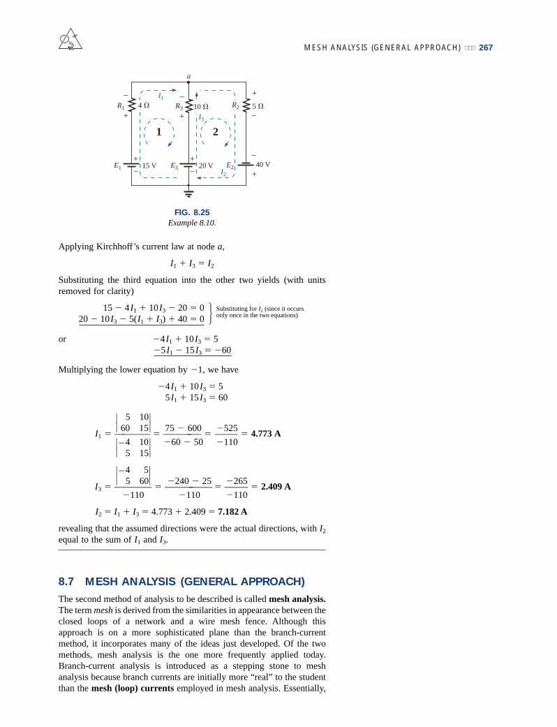
EXAMPLE 8.10 Apply branch-current analysis to the network of Fig.8.25.
Solution: Again, the current directions were chosen to match the“pressure” of each battery. The polarities are then added and Kirch-hoff’s voltage law is applied around each closed loop in the clockwisedirection. The result is as follows:
loop 1: 15 V (4 )I1 (10 )I3 20 V 0
loop 2: 20 V (10 )I3 (5 )I2 40 V 0
4
6 V
–
+
I1 = 1 A
E2
–
+–
+1
2 VE1
–
+
–
+
2
R3
R1 R2
I2 = 2 A
I3 = 1 A
FIG. 8.24
Reviewing the results of the analysis of the network of Fig. 8.21.
MESH ANALYSIS (GENERAL APPROACH) 267
Applying Kirchhoff’s current law at node a,
I1 I3 I2
Substituting the third equation into the other two yields (with unitsremoved for clarity)
15 4 I1 10 I3 20 0 Substituting for I2 (since it occurs
20 10 I3 5(I1 I3) 40 0 only once in the two equations)
or 4 I1 10 I3 55 I1 15 I3 60
Multiplying the lower equation by 1, we have
4 I1 10 I3 55 I1 15 I3 60
5 10 60 15 75 600 525
I1 –––––––– ––––––––– ––––– 4.773 A4 10 60 50 110 5 15
4 5 5 60 240 25 265
I3 –––––––– –––––––—–– ––—– 2.409 A110 110 110
I2 I1 I3 4.773 2.409 7.182 A
revealing that the assumed directions were the actual directions, with I2
equal to the sum of I1 and I3.
8.7 MESH ANALYSIS (GENERAL APPROACH)
The second method of analysis to be described is called mesh analysis.The term mesh is derived from the similarities in appearance between theclosed loops of a network and a wire mesh fence. Although thisapproach is on a more sophisticated plane than the branch-currentmethod, it incorporates many of the ideas just developed. Of the twomethods, mesh analysis is the one more frequently applied today.Branch-current analysis is introduced as a stepping stone to meshanalysis because branch currents are initially more “real” to the studentthan the mesh (loop) currents employed in mesh analysis. Essentially,
NA
I1
5 R1
I2
I3
a
R2R3 10
+
–+
–4
40 VE2+
–15 VE1 –
+20 VE3 –
+
21
–
+
FIG. 8.25
Example 8.10.
268 METHODS OF ANALYSIS AND SELECTED TOPICS (dc)
the mesh-analysis approach simply eliminates the need to substitute theresults of Kirchhoff’s current law into the equations derived fromKirchhoff’s voltage law. It is now accomplished in the initial writing ofthe equations. The systematic approach outlined below should be fol-lowed when applying this method.
1. Assign a distinct current in the clockwise direction to eachindependent, closed loop of the network. It is not absolutelynecessary to choose the clockwise direction for each loop current.In fact, any direction can be chosen for each loop current with noloss in accuracy, as long as the remaining steps are followedproperly. However, by choosing the clockwise direction as astandard, we can develop a shorthand method (Section 8.8) forwriting the required equations that will save time and possiblyprevent some common errors.
This first step is accomplished most effectively by placing a loopcurrent within each “window” of the network, as demonstrated in theprevious section, to ensure that they are all independent. A variety ofother loop currents can be assigned. In each case, however, be sure thatthe information carried by any one loop equation is not included in acombination of the other network equations. This is the crux of the ter-minology: independent. No matter how you choose your loop currents,the number of loop currents required is always equal to the number ofwindows of a planar (no-crossovers) network. On occasion a networkmay appear to be nonplanar. However, a redrawing of the network mayreveal that it is, in fact, planar. Such may be the case in one or twoproblems at the end of the chapter.
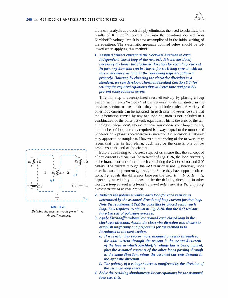
Before continuing to the next step, let us ensure that the concept ofa loop current is clear. For the network of Fig. 8.26, the loop current I1
is the branch current of the branch containing the 2- resistor and 2-Vbattery. The current through the 4- resistor is not I1, however, sincethere is also a loop current I2 through it. Since they have opposite direc-tions, I4 equals the difference between the two, I1 I2 or I2 I1,depending on which you choose to be the defining direction. In otherwords, a loop current is a branch current only when it is the only loopcurrent assigned to that branch.
2. Indicate the polarities within each loop for each resistor asdetermined by the assumed direction of loop current for that loop.Note the requirement that the polarities be placed within eachloop. This requires, as shown in Fig. 8.26, that the 4- resistorhave two sets of polarities across it.
3. Apply Kirchhoff’s voltage law around each closed loop in theclockwise direction. Again, the clockwise direction was chosen toestablish uniformity and prepare us for the method to beintroduced in the next section.a. If a resistor has two or more assumed currents through it,
the total current through the resistor is the assumed currentof the loop in which Kirchhoff’s voltage law is being applied,plus the assumed currents of the other loops passing throughin the same direction, minus the assumed currents through inthe opposite direction.
b. The polarity of a voltage source is unaffected by the direction ofthe assigned loop currents.
4. Solve the resulting simultaneous linear equations for the assumedloop currents.
NA
FIG. 8.26
Defining the mesh currents for a “two-window” network.
I1
1 R1
I2
R2
+
–+
–2
6 V E2
+
–2 VE1 –
+
21 R3 4
+
–
–
+
I3
MESH ANALYSIS (GENERAL APPROACH) 269
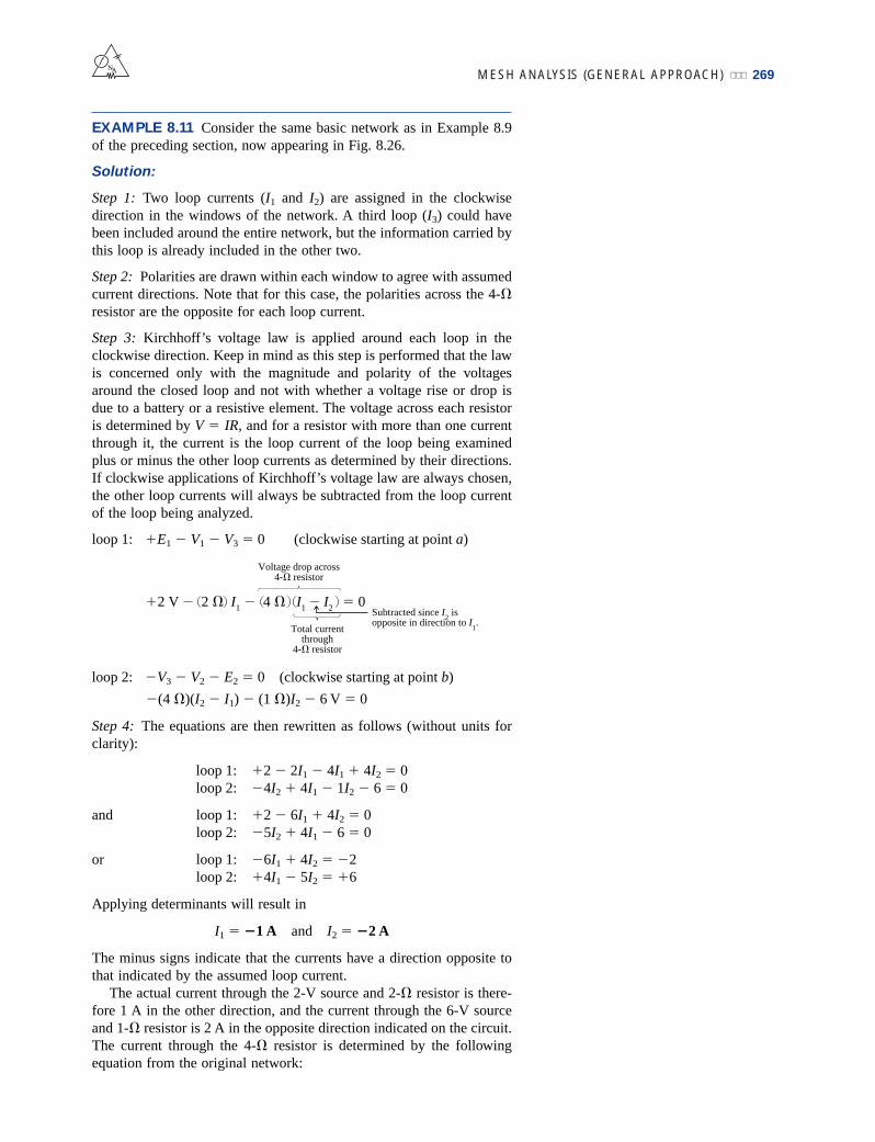
EXAMPLE 8.11 Consider the same basic network as in Example 8.9of the preceding section, now appearing in Fig. 8.26.
Solution:
Step 1: Two loop currents (I1 and I2) are assigned in the clockwisedirection in the windows of the network. A third loop (I3) could havebeen included around the entire network, but the information carried bythis loop is already included in the other two.
Step 2: Polarities are drawn within each window to agree with assumedcurrent directions. Note that for this case, the polarities across the 4-resistor are the opposite for each loop current.
Step 3: Kirchhoff’s voltage law is applied around each loop in theclockwise direction. Keep in mind as this step is performed that the lawis concerned only with the magnitude and polarity of the voltagesaround the closed loop and not with whether a voltage rise or drop isdue to a battery or a resistive element. The voltage across each resistoris determined by V IR, and for a resistor with more than one currentthrough it, the current is the loop current of the loop being examinedplus or minus the other loop currents as determined by their directions.If clockwise applications of Kirchhoff’s voltage law are always chosen,the other loop currents will always be subtracted from the loop currentof the loop being analyzed.
loop 1: E1 V1 V3 0 (clockwise starting at point a)
loop 2: V3 V2 E2 0 (clockwise starting at point b)
(4 )(I2 I1) (1 )I2 6 V 0
Step 4: The equations are then rewritten as follows (without units forclarity):
loop 1: 2 2I1 4I1 4I2 0loop 2: 4I2 4I1 1I2 6 0
and loop 1: 2 6I1 4I2 0loop 2: 5I2 4I1 6 0
or loop 1: 6I1 4I2 2loop 2: 4I1 5I2 6
Applying determinants will result in
I1 1 A and I2 2 A
The minus signs indicate that the currents have a direction opposite tothat indicated by the assumed loop current.
The actual current through the 2-V source and 2- resistor is there-fore 1 A in the other direction, and the current through the 6-V sourceand 1- resistor is 2 A in the opposite direction indicated on the circuit.The current through the 4- resistor is determined by the followingequation from the original network:
2 V 2 I1 4 I1 I2 0
Total currentthrough
4- resistor
Voltage drop across4- resistor
Subtracted since I2 is
opposite in direction to I1.
NA
270 METHODS OF ANALYSIS AND SELECTED TOPICS (dc)
loop 1: I4 I1 I2 1 A (2 A) 1 A 2 A 1 A (in the direction of I1)
The outer loop (I3) and one inner loop (either I1 or I2) would alsohave produced the correct results. This approach, however, will oftenlead to errors since the loop equations may be more difficult to write.The best method of picking these loop currents is to use the windowapproach.
EXAMPLE 8.12 Find the current through each branch of the networkof Fig. 8.27.
Solution:
Steps 1 and 2 are as indicated in the circuit. Note that the polarities ofthe 6- resistor are different for each loop current.
Step 3: Kirchhoff’s voltage law is applied around each closed loop inthe clockwise direction:
loop 1: E1 V1 V2 E2 0 (clockwise starting at point a)
5 V (1 )I1 (6 )(I1 I2) 10 V 0
I2 flows through the 6-Q resistorin the direction opposite to I1.
loop 2: E2 V2 V3 0 (clockwise starting at point b)
10 V (6 )(I2 I1) (2 )I2 0
The equations are rewritten as
5 I1 6I1 6I2 10 0 7I1 6I2 510 6I2 6I1 2I2 0 6I1 8I2 10
Step 4: 5 6 10 8 40 60 20
I1 –––––––––– ––––––––– ––– 1 A 7 6 56 36 20 6 8
7 5 6 10 70 30 40
I2 –––––––––– ––––––– –– 2 A20 20 20
Since I1 and I2 are positive and flow in opposite directions throughthe 6- resistor and 10-V source, the total current in this branch isequal to the difference of the two currents in the direction of thelarger:
I2 > I1 (2 A > 1 A)
Therefore,
IR2 I2 I1 2 A 1 A 1 A in the direction of I2
It is sometimes impractical to draw all the branches of a circuit atright angles to one another. The next example demonstrates how a por-tion of a network may appear due to various constraints. The method ofanalysis does not change with this change in configuration.
NA
R1 R2 6 +
–1
5 VE1 –
+10 VE2 –
+
21
+
–
a
2
I2
+
–
–
+
bI1
R3
FIG. 8.27
Example 8.12.

MESH ANALYSIS (GENERAL APPROACH) 271
6 104 1 6 40 34
I2 ––––––– –––––––– –––– 0.773 A44 44 44
The current in the 4- resistor and 4-V source for loop 1 is
I1 I2 2.182 A (0.773 A) 2.182 A 0.773 A 1.409 A
revealing that it is 1.409 A in a direction opposite (due to the minussign) to I1 in loop 1.
Supermesh Currents
On occasion there will be current sources in the network to which meshanalysis is to be applied. In such cases one can convert the currentsource to a voltage source (if a parallel resistor is present) and proceedas before or utilize a supermesh current and proceed as follows.
Start as before and assign a mesh current to each independent loop,including the current sources, as if they were resistors or voltagesources. Then mentally (redraw the network if necessary) remove thecurrent sources (replace with open-circuit equivalents), and apply
NA
a
R1 = 2
2 +
–
E2 4 V
R3 = 6 –
+
E1 = 6 V+
– +–
bI1 I2
E3 = 3 V1 2
R2 4
+
–
–
+
FIG. 8.28
Example 8.13.
det[[10,4][1,10]]/det[[6,4][4,10]] ENTER 2.182
CALC. 8.2
EXAMPLE 8.13 Find the branch currents of the network of Fig. 8.28.
Solution:
Steps 1 and 2 are as indicated in the circuit.
Step 3: Kirchhoff’s voltage law is applied around each closed loop:
loop 1: E1 I1R1 E2 V2 0 (clockwise from point a)
6 V (2 )I1 4 V (4 )(I1 I2) 0
loop 2: V2 E2 V3 E3 0 (clockwise from point b)
(4 )(I2 I1) 4 V (6 )(I2) 3 V 0
which are rewritten as
10 4I1 2I1 4I2 0 6I1 4I2 10 1 4I1 4I2 6I2 0 4I1 10I2 1
or, by multiplying the top equation by 1, we obtain
6I1 4I2 104I1 10I2 1
Step 4: 10 4 1 10 100 4 96I1 ––––––––––– ––––––––– –––– 2.182 A 6 4 60 16 44 4 10
Using the TI-86 calculator:

272 METHODS OF ANALYSIS AND SELECTED TOPICS (dc)
Kirchhoff’s voltage law to all the remaining independent paths of thenetwork using the mesh currents just defined. Any resulting path,including two or more mesh currents, is said to be the path of a super-mesh current. Then relate the chosen mesh currents of the network tothe independent current sources of the network, and solve for the meshcurrents. The next example will clarify the definition of a supermeshcurrent and the procedure.
EXAMPLE 8.14 Using mesh analysis, determine the currents of thenetwork of Fig. 8.29.
NA
Solution: First, the mesh currents for the network are defined, asshown in Fig. 8.30. Then the current source is mentally removed, asshown in Fig. 8.31, and Kirchhoff’s voltage law is applied to the result-ing network. The single path now including the effects of two mesh cur-rents is referred to as the path of a supermesh current.
R1 6
E1 20 V
E2 12 V4 AI
R2
4
R3
2
FIG. 8.29
Example 8.14.
R1 6
E1 20 V
E2 12 V4 AI
R2
4
R3
2
I1 I2
a
FIG. 8.30
Defining the mesh currents for the network of Fig. 8.29.
E1 20 V
E2 12 VI1 I2
+ – + –
+
–
R2
4
R3
2 R1 6
Supermeshcurrent
FIG. 8.31
Defining the supermesh current.
Applying Kirchhoff’s law:
20 V I1(6 ) I1(4 ) I2(2 ) 12 V 0
or 10I1 2I2 32
MESH ANALYSIS (GENERAL APPROACH) 273
Node a is then used to relate the mesh currents and the currentsource using Kirchhoff’s current law:
I1 I I2
The result is two equations and two unknowns:
10I1 2I2 32I1 I2 4
Applying determinants:
32 2 4 1 (32)(1) (2)(4) 40
I1 –––––––– ––––––––––––––– ––– 3.33 A10 2 (10)(1) (2)(1) 12 1 1
and I2 I1 I 3.33 A 4 A 0.67 A
In the above analysis, it might appear that when the current sourcewas removed, I1 I2. However, the supermesh approach requires thatwe stick with the original definition of each mesh current and not alterthose definitions when current sources are removed.
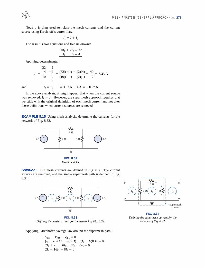
EXAMPLE 8.15 Using mesh analysis, determine the currents for thenetwork of Fig. 8.32.
NA
I1 I3I22 8
6
6 A 8 A
FIG. 8.33
Defining the mesh currents for the network of Fig. 8.32.
Supermeshcurrent
I1 I3I22 8
6 + –
+
–
–
+
FIG. 8.34
Defining the supermesh current for thenetwork of Fig. 8.32.
2 8
6
6 A 8 A
FIG. 8.32
Example 8.15.
Solution: The mesh currents are defined in Fig. 8.33. The currentsources are removed, and the single supermesh path is defined in Fig.8.34.
Applying Kirchhoff’s voltage law around the supermesh path:
V2 V6 V8 0(I2 I1)2 I2(6 ) (I2 I3)8 02I2 2I1 6I2 8I2 8I3 0
2I1 16I2 8I3 0

274 METHODS OF ANALYSIS AND SELECTED TOPICS (dc)NA
Introducing the relationship between the mesh currents and the cur-rent sources:
I1 6 A
I3 8 A
results in the following solutions:
2I1 16I2 8I3 0
2(6 A) 16I2 8(8 A) 0
and I2 4.75 A
Then I2 I1 I2 6 A 4.75 A 1.25 A
and I8 I3 I2 8 A 4.75 A 3.25 A
Again, note that you must stick with your original definitions of thevarious mesh currents when applying Kirchhoff’s voltage law aroundthe resulting supermesh paths.
8.8 MESH ANALYSIS (FORMAT APPROACH)
Now that the basis for the mesh-analysis approach has been established,we will now examine a technique for writing the mesh equations morerapidly and usually with fewer errors. As an aid in introducing the pro-cedure, the network of Example 8.12 (Fig. 8.27) has been redrawn inFig. 8.35 with the assigned loop currents. (Note that each loop currenthas a clockwise direction.)
The equations obtained are
7I1 6I2 56I1 8I2 10
which can also be written as
7I1 6I2 58I2 6I1 10
and expanded as
Col. 1 Col. 2 Col. 3
(1 6)I1 6I2 (5 10)(2 6)I2 6I1 10
Note in the above equations that column 1 is composed of a loopcurrent times the sum of the resistors through which that loop currentpasses. Column 2 is the product of the resistors common to anotherloop current times that other loop current. Note that in each equation,this column is subtracted from column 1. Column 3 is the algebraicsum of the voltage sources through which the loop current of interestpasses. A source is assigned a positive sign if the loop current passesfrom the negative to the positive terminal, and a negative value isassigned if the polarities are reversed. The comments above are correctonly for a standard direction of loop current in each window, the onechosen being the clockwise direction.
The above statements can be extended to develop the following for-mat approach to mesh analysis:
76 A
16
I1 I2
21 2 R3
+
–
–R1
+1 R2 6
+
–
–
+
5 VE1 –
+10 VE2 –
+
FIG. 8.35
Network of Fig. 8.27 redrawn with assignedloop currents.

MESH ANALYSIS (FORMAT APPROACH) 275
1. Assign a loop current to each independent, closed loop (as in theprevious section) in a clockwise direction.
2. The number of required equations is equal to the number ofchosen independent, closed loops. Column 1 of each equation isformed by summing the resistance values of those resistorsthrough which the loop current of interest passes and multiplyingthe result by that loop current.
3. We must now consider the mutual terms, which, as noted in theexamples above, are always subtracted from the first column. Amutual term is simply any resistive element having an additionalloop current passing through it. It is possible to have more than onemutual term if the loop current of interest has an element in commonwith more than one other loop current. This will be demonstrated inan example to follow. Each term is the product of the mutual resistorand the other loop current passing through the same element.
4. The column to the right of the equality sign is the algebraic sum ofthe voltage sources through which the loop current of interestpasses. Positive signs are assigned to those sources of voltagehaving a polarity such that the loop current passes from thenegative to the positive terminal. A negative sign is assigned tothose potentials for which the reverse is true.
5. Solve the resulting simultaneous equations for the desired loopcurrents.
Before considering a few examples, be aware that since the columnto the right of the equals sign is the algebraic sum of the voltage sourcesin that loop, the format approach can be applied only to networks inwhich all current sources have been converted to their equivalent volt-age source.
EXAMPLE 8.16 Write the mesh equations for the network of Fig.8.36, and find the current through the 7- resistor.
Solution:
Step 1: As indicated in Fig. 8.36, each assigned loop current has aclockwise direction.
Steps 2 to 4:
I1: (8 6 2 )I1 (2 )I2 4 VI2: (7 2 )I2 (2 )I1 9 V
and 16I1 2I2 49I2 2I1 9
which, for determinants, are
16I1 2I2 42I1 9I2 9
16 42 9 144 8 136
and I2 I7 ––––––––– ––––––––– ––––– 16 2 144 4 1402 9
0.971 A
NA
I1 I2
21
4 V–+
6
–+
–
+8 7
+
–2
+
–
–
+
9 V+–
FIG. 8.36
Example 8.16.

276 METHODS OF ANALYSIS AND SELECTED TOPICS (dc)
Solution:
Step 1: Each window is assigned a loop current in the clockwise direc-tion:
Summing terms yields
2I1 I2 0 26I2 I1 3I3 47I3 3I2 0 2
which are rewritten for determinants as
Note that the coefficients of the a and b diagonals are equal. Thissymmetry about the c-axis will always be true for equations writtenusing the format approach. It is a check on whether the equations wereobtained correctly.
We will now consider a network with only one source of voltage topoint out that mesh analysis can be used to advantage in other than multi-source networks.
2I1 I2 0 2
0 3I2 7I3 2
I1 6I2 3I3 4
c b a
b
a
1 1 I1 1 I2 0 2 V 4 V
3 4 I3 3 I2 0 2 V1 2 3 I2 1 I1 3 I3 4 V
I1 :I2 :I3 :
I1 does not pass through an element
mutual with I3.
I3 does not pass through an element
mutual with I1.
NA
I1 I2
21
1
+
–
–
+
4 V–
+
–
+
+
–
–2 V
+
+
–1
+2 V
–
–
+4
3 3
2 + –
I3
FIG. 8.37
Example 8.17.
EXAMPLE 8.17 Write the mesh equations for the network of Fig.8.37.
MESH ANALYSIS (FORMAT APPROACH) 277
Solution 1:
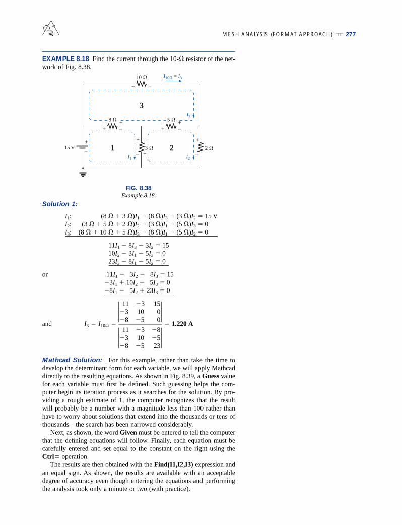
I1: (8 3 )I1 (8 )I3 (3 )I2 15 VI2: (3 5 2 )I2 (3 )I1 (5 )I3 0I3: (8 10 5 )I3 (8 )I1 (5 )I2 0
11I1 8I3 3I2 1510I2 3I1 5I3 023I3 8I1 5I2 0
or 11I1 3I2 8I3 153I1 10I2 5I3 08I1 5I2 23I3 0
11 3 153 10 08 5 0
and I3 I10 ––––––––––––– 1.220 A 11 3 83 10 58 5 23
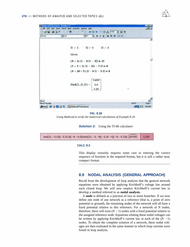
Mathcad Solution: For this example, rather than take the time todevelop the determinant form for each variable, we will apply Mathcaddirectly to the resulting equations. As shown in Fig. 8.39, a Guess valuefor each variable must first be defined. Such guessing helps the com-puter begin its iteration process as it searches for the solution. By pro-viding a rough estimate of 1, the computer recognizes that the resultwill probably be a number with a magnitude less than 100 rather thanhave to worry about solutions that extend into the thousands or tens ofthousands—the search has been narrowed considerably.
Next, as shown, the word Given must be entered to tell the computerthat the defining equations will follow. Finally, each equation must becarefully entered and set equal to the constant on the right using theCtrl operation.
The results are then obtained with the Find(I1,I2,I3) expression andan equal sign. As shown, the results are available with an acceptabledegree of accuracy even though entering the equations and performingthe analysis took only a minute or two (with practice).
NA
I1 I2
21 2
+
–3
+
–
–
+
–++–
+
–15 V
–++–
10
–+
3I3
I10 = I3
8 5
FIG. 8.38
Example 8.18.
EXAMPLE 8.18 Find the current through the 10- resistor of the net-work of Fig. 8.38.
278 METHODS OF ANALYSIS AND SELECTED TOPICS (dc)NA
det[[11,3,15][3,10,0][8,5,0]]/det[[11,3,8][3,10,5][8,5,23]] ENTER 1.220
CALC. 8.3
Solution 2: Using the TI-86 calculator:
FIG. 8.39
Using Mathcad to verify the numerical calculations of Example 8.18.
This display certainly requires some care in entering the correctsequence of brackets in the required format, but it is still a rather neat,compact format.
8.9 NODAL ANALYSIS (GENERAL APPROACH)
Recall from the development of loop analysis that the general networkequations were obtained by applying Kirchhoff’s voltage law aroundeach closed loop. We will now employ Kirchhoff’s current law todevelop a method referred to as nodal analysis.
A node is defined as a junction of two or more branches. If we nowdefine one node of any network as a reference (that is, a point of zeropotential or ground), the remaining nodes of the network will all have afixed potential relative to this reference. For a network of N nodes,therefore, there will exist (N 1) nodes with a fixed potential relative tothe assigned reference node. Equations relating these nodal voltages canbe written by applying Kirchhoff’s current law at each of the (N 1)nodes. To obtain the complete solution of a network, these nodal volt-ages are then evaluated in the same manner in which loop currents werefound in loop analysis.
NODAL ANALYSIS (GENERAL APPROACH) 279NA
The nodal analysis method is applied as follows:
1. Determine the number of nodes within the network.2. Pick a reference node, and label each remaining node with a
subscripted value of voltage: V1, V2, and so on.3. Apply Kirchhoff’s current law at each node except the reference.
Assume that all unknown currents leave the node for eachapplication of Kirchhoff’s current law. In other words, for eachnode, don’t be influenced by the direction that an unknowncurrent for another node may have had. Each node is to be treatedas a separate entity, independent of the application of Kirchhoff’scurrent law to the other nodes.
4. Solve the resulting equations for the nodal voltages.
A few examples will clarify the procedure defined by step 3. It willinitially take some practice writing the equations for Kirchhoff’s cur-rent law correctly, but in time the advantage of assuming that all thecurrents leave a node rather than identifying a specific direction foreach branch will become obvious. (The same type of advantage is asso-ciated with assuming that all the mesh currents are clockwise whenapplying mesh analysis.)
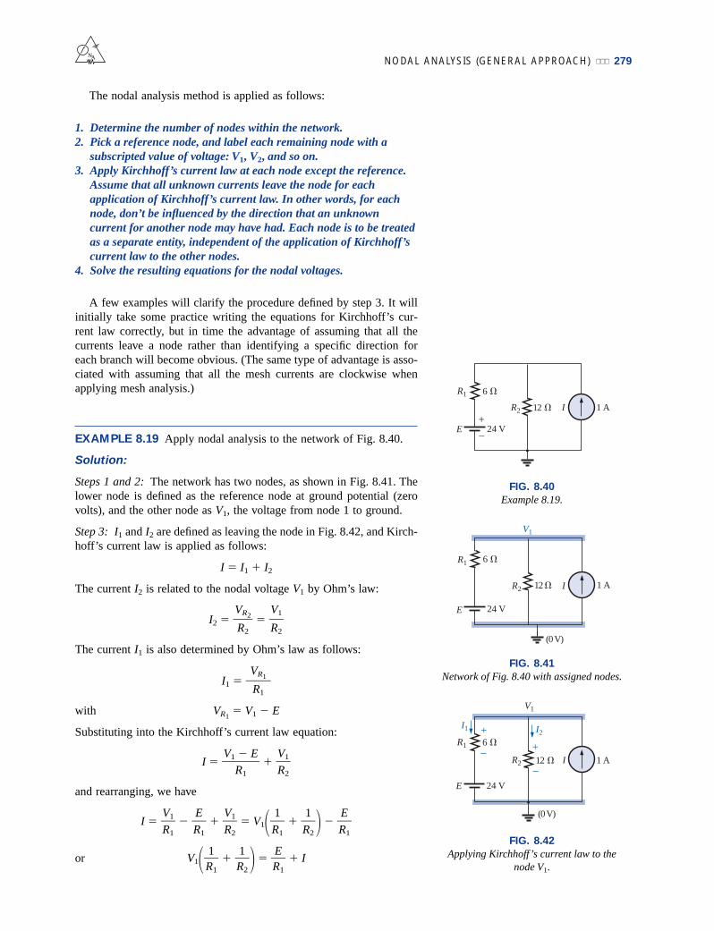
EXAMPLE 8.19 Apply nodal analysis to the network of Fig. 8.40.
Solution:
Steps 1 and 2: The network has two nodes, as shown in Fig. 8.41. Thelower node is defined as the reference node at ground potential (zerovolts), and the other node as V1, the voltage from node 1 to ground.
Step 3: I1 and I2 are defined as leaving the node in Fig. 8.42, and Kirch-hoff’s current law is applied as follows:
I I1 I2
The current I2 is related to the nodal voltage V1 by Ohm’s law:
I2
The current I1 is also determined by Ohm’s law as follows:
I1
with VR1 V1 E
Substituting into the Kirchhoff’s current law equation:
I
and rearranging, we have
I V1
or V1 IER1
1R2
1R1
ER1
1R2
1R1
V1R2
ER1
V1R1
V1R2
V1 E
R1
VR1R1
V1R2
VR2R2
I 1 A12 R2
R1 6
E 24 V–
+
FIG. 8.40
Example 8.19.
I 1 A12 R2
R1 6
E 24 V
V1
(0 V)
FIG. 8.41
Network of Fig. 8.40 with assigned nodes.
+
–I 1 A12 R2
R1 6
E 24 V
V1
(0 V)
I1
–
+
I2
FIG. 8.42
Applying Kirchhoff’s current law to the node V1.
280 METHODS OF ANALYSIS AND SELECTED TOPICS (dc)
Substituting numerical values, we obtain
V1 1 A 4 A 1 A24 V6
112
16
NA
R2
R1
4
R3
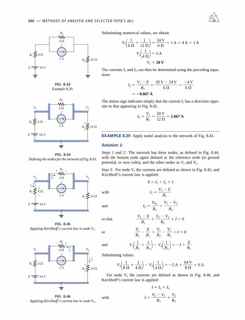
E 64 V
8 2 A
I
10
FIG. 8.43
Example 8.20.
R2
R1
4
R3
E 64 V
8 2 A
I
10
+
–
V2V1
FIG. 8.44
Defining the nodes for the network of Fig. 8.43.
R2
R1
4
R3
E 64 V
8 2 A
I
10
+ –
+
–
V2V1
I1
I2
FIG. 8.45
Applying Kirchhoff’s current law to node V1.
R2
R1
4
R3
E 64 V
8 2 A
I
10
+–
+
–
V2V1
I3
I2
FIG. 8.46
Applying Kirchhoff’s current law to node V2.
V1 5 A
V1 20 V
The currents I1 and I2 can then be determined using the preceding equa-tions:
I1
0.667 A
The minus sign indicates simply that the current I1 has a direction oppo-site to that appearing in Fig. 8.42.
I2 1.667 A
EXAMPLE 8.20 Apply nodal analysis to the network of Fig. 8.43.
Solution 1:
Steps 1 and 2: The network has three nodes, as defined in Fig. 8.44,with the bottom node again defined as the reference node (at groundpotential, or zero volts), and the other nodes as V1 and V2.
Step 3: For node V1 the currents are defined as shown in Fig. 8.45, andKirchhoff’s current law is applied:
0 I1 I2 I
with I1
and I2
so that I 0
or I 0
and V1 V2 I
Substituting values:
V1 V2 2 A 6 A
For node V2 the currents are defined as shown in Fig. 8.46, andKirchhoff’s current law is applied:
I I2 I3
with I V2R3
V2 V1
R2
64 V8
14
14
18
ER1
1R2
1R2
1R1
V2R2
V1R2
ER1
V1R1
V1 V2
R2
V1 E
R1
V1 V2
R2
VR2R2
V1 E
R1
20 V12
V1R2
4 V
6
20 V 24 V
6
V1 E
R1
14
NODAL ANALYSIS (GENERAL APPROACH) 281
or I
and V2 V1 I
Substituting values:
V2 V1 2 A
Step 4: The result is two equations and two unknowns:
V1 V2 6 A
V1 V2 2 A
which become
0.375V1 0.25V2 60.25V1 0.35V2 2
Using determinants,
V1 37.818 V
V2 32.727 V
Since E is greater than V1, the current I1 flows from ground to V1 and isequal to
IR1 3.273 A
The positive value for V2 results in a current IR3from node V2 to ground
equal to
IR3 3.273 A
Since V1 is greater than V2, the current IR2flows from V1 to V2 and is
equal to
IR2 1.273 A
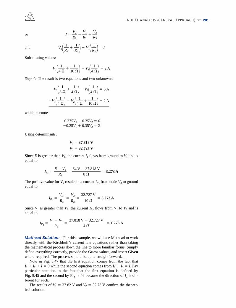
Mathcad Solution: For this example, we will use Mathcad to workdirectly with the Kirchhoff’s current law equations rather than takingthe mathematical process down the line to more familiar forms. Simplydefine everything correctly, provide the Guess values, and insert Givenwhere required. The process should be quite straightforward.
Note in Fig. 8.47 that the first equation comes from the fact that I1 I2 I 0 while the second equation comes from I2 I3 I. Payparticular attention to the fact that the first equation is defined by Fig. 8.45 and the second by Fig. 8.46 because the direction of I2 is dif-ferent for each.
The results of V1 37.82 V and V2 32.73 V confirm the theoret-ical solution.
37.818 V 32.727 V
4
V1 V2
R2
32.727 V
10
V2R3
VR3R3
64 V 37.818 V
8
E V1
R1
110
14
14
14
14
18
14
110
14
1R2
1R3
1R2
V2R3
V1R2
V2R2
NA
282 METHODS OF ANALYSIS AND SELECTED TOPICS (dc)
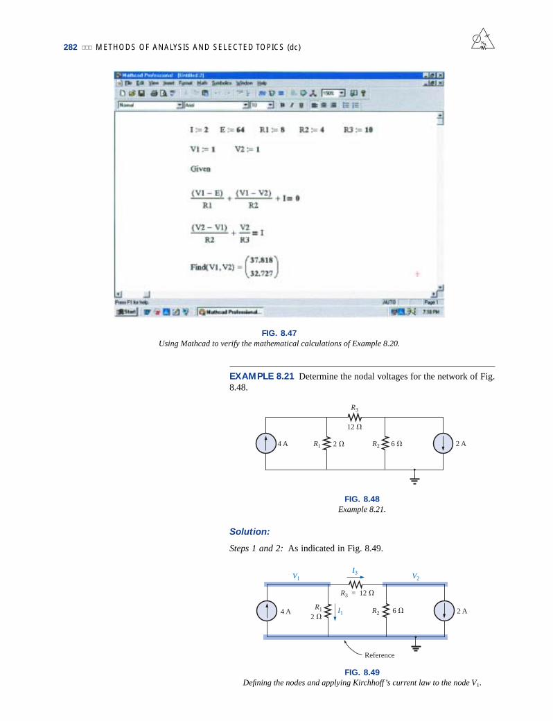
EXAMPLE 8.21 Determine the nodal voltages for the network of Fig.8.48.
NA
4 A 2 R1 R2 6
R3
2 A
12
FIG. 8.48
Example 8.21.
4 AR1 2 A
2
I3
Reference
V1 V2
R2 6
R3 = 12
I1
FIG. 8.49
Defining the nodes and applying Kirchhoff’s current law to the node V1.
Solution:
Steps 1 and 2: As indicated in Fig. 8.49.
FIG. 8.47
Using Mathcad to verify the mathematical calculations of Example 8.20.
NODAL ANALYSIS (GENERAL APPROACH) 283NA
4 A R1 2 A2
I3
Reference
V1 V2
R26
R3 = 12
I2
FIG. 8.50
Applying Kirchhoff’s current law to the node V2.
Step 3: Included in Fig. 8.49 for the node V1. Applying Kirchhoff’scurrent law:
4 A I1 I3
and 4 A
Expanding and rearranging:
V1 V2 4 A
For node V2 the currents are defined as in Fig. 8.50.
112
112
12
V1 V2
12
V12
V1 V2
R3
V1R1
Applying Kirchhoff’s current law:
0 I3 I2 2 A
and 2 A 0 2 A 0
Expanding and rearranging:
V2 V1 2 A
resulting in two equations and two unknowns (numbered for later refer-ence):
V1 V2 4 A
V2 V1 2 A
(8.3)
producing
V1 V2 4 7V1 V2 48
V1 V2 2 1V1 3V2 24
48 124 3
and V1 –––––––––– 6 V7 11 03
7 481 24
V2 –––––––––– 6 V20
120
20
12020
312
112
112
712
112
16
112
112
112
12
112
16
112
V26
V2 V1
12
V2R2
V2 V1
R3
284 METHODS OF ANALYSIS AND SELECTED TOPICS (dc)
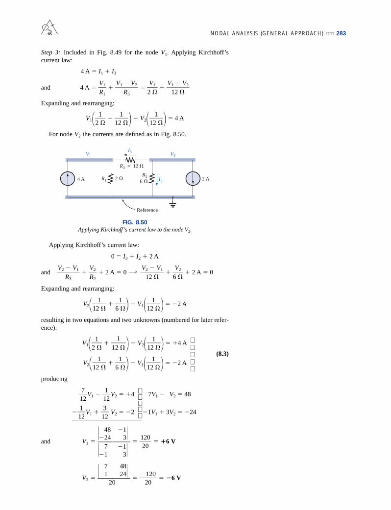
Since V1 is greater than V2, the current through R3 passes from V1 to V2.Its value is
IR3 1 A
The fact that V1 is positive results in a current IR1from V1 to ground
equal to
IR1 3 A
Finally, since V2 is negative, the current IR2flows from ground to V2 and
is equal to
IR2 1 A
Supernode
On occasion there will be independent voltage sources in the network towhich nodal analysis is to be applied. In such cases we can convert thevoltage source to a current source (if a series resistor is present) and pro-ceed as before, or we can introduce the concept of a supernode and pro-ceed as follows.
Start as before and assign a nodal voltage to each independent node ofthe network, including each independent voltage source as if it were aresistor or current source. Then mentally replace the independent voltagesources with short-circuit equivalents, and apply Kirchhoff’s current lawto the defined nodes of the network. Any node including the effect of ele-ments tied only to other nodes is referred to as a supernode (since it hasan additional number of terms). Finally, relate the defined nodes to theindependent voltage sources of the network, and solve for the nodal volt-ages. The next example will clarify the definition of supernode.
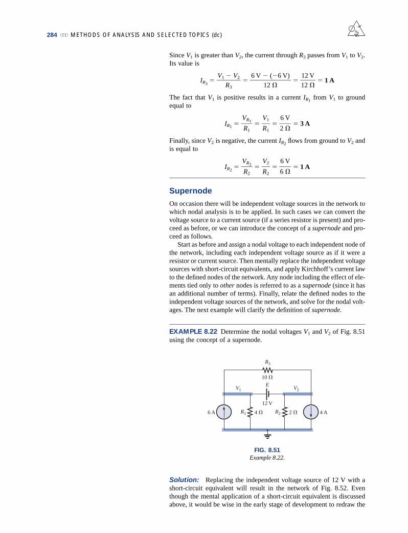
EXAMPLE 8.22 Determine the nodal voltages V1 and V2 of Fig. 8.51using the concept of a supernode.
6 V6
V2R2
VR2R2
6 V2
V1R1
VR1R1
12 V12
6 V (6 V)
12
V1 V2
R3
NA
R1 4
R3
10 E
12 V
R2 2 6 A 4 A
V2V1
FIG. 8.51
Example 8.22.
Solution: Replacing the independent voltage source of 12 V with ashort-circuit equivalent will result in the network of Fig. 8.52. Eventhough the mental application of a short-circuit equivalent is discussedabove, it would be wise in the early stage of development to redraw the
NODAL ANALYSIS (GENERAL APPROACH) 285NA
R1 4
R3
10
R2 2 6 A 4 A
V2V1
I1 I2
I3 I3Supernode
FIG. 8.52
Defining the supernode for the network of Fig. 8.51.
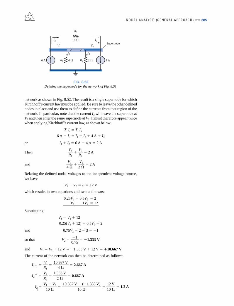
network as shown in Fig. 8.52. The result is a single supernode for whichKirchhoff’s current law must be applied. Be sure to leave the other definednodes in place and use them to define the currents from that region of thenetwork. In particular, note that the current I3 will leave the supernode atV1 and then enter the same supernode at V2. It must therefore appear twicewhen applying Kirchhoff’s current law, as shown below:
Σ Ii Σ Io
6 A I3 I1 I2 4 A I3
or I1 I2 6 A 4 A 2 A
Then 2 A
and 2 A
Relating the defined nodal voltages to the independent voltage source,we have
V1 V2 E 12 V
which results in two equations and two unknowns:
0.25V1 0.5V2 2V1 1V2 12
Substituting:
V1 V2 12
0.25(V2 12) 0.5V2 2
and 0.75V2 2 3 1
so that V2 1.333 V
and V1 V2 12 V 1.333 V 12 V 10.667 V
The current of the network can then be determined as follows:
I1 2.667 A
I2 0.667 A
I3 1.2 A12 V10
10.667 V (1.333 V)
10
V1 V2
10
1.333 V
2
V2R2
10.667 V
4
VR1
10.75
V22
V14
V2R2
V1R1
NA286 METHODS OF ANALYSIS AND SELECTED TOPICS (dc)
A careful examination of the network at the beginning of the analy-sis would have revealed that the voltage across the resistor R3 must be12 V and I3 must be equal to 1.2 A.
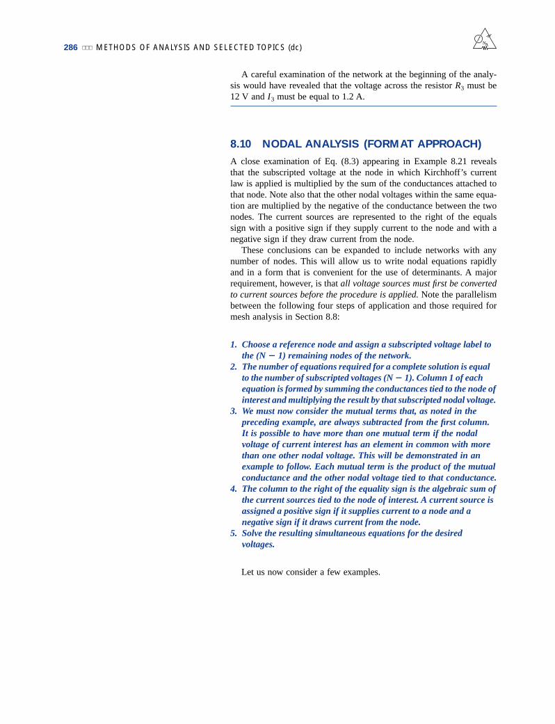
8.10 NODAL ANALYSIS (FORMAT APPROACH)
A close examination of Eq. (8.3) appearing in Example 8.21 revealsthat the subscripted voltage at the node in which Kirchhoff’s currentlaw is applied is multiplied by the sum of the conductances attached tothat node. Note also that the other nodal voltages within the same equa-tion are multiplied by the negative of the conductance between the twonodes. The current sources are represented to the right of the equalssign with a positive sign if they supply current to the node and with anegative sign if they draw current from the node.
These conclusions can be expanded to include networks with anynumber of nodes. This will allow us to write nodal equations rapidlyand in a form that is convenient for the use of determinants. A majorrequirement, however, is that all voltage sources must first be convertedto current sources before the procedure is applied. Note the parallelismbetween the following four steps of application and those required formesh analysis in Section 8.8:
1. Choose a reference node and assign a subscripted voltage label tothe (N 1) remaining nodes of the network.
2. The number of equations required for a complete solution is equalto the number of subscripted voltages (N 1). Column 1 of eachequation is formed by summing the conductances tied to the node ofinterest and multiplying the result by that subscripted nodal voltage.
3. We must now consider the mutual terms that, as noted in thepreceding example, are always subtracted from the first column.It is possible to have more than one mutual term if the nodalvoltage of current interest has an element in common with morethan one other nodal voltage. This will be demonstrated in anexample to follow. Each mutual term is the product of the mutualconductance and the other nodal voltage tied to that conductance.
4. The column to the right of the equality sign is the algebraic sum ofthe current sources tied to the node of interest. A current source isassigned a positive sign if it supplies current to a node and anegative sign if it draws current from the node.
5. Solve the resulting simultaneous equations for the desiredvoltages.
Let us now consider a few examples.
NODAL ANALYSIS (FORMAT APPROACH) 287
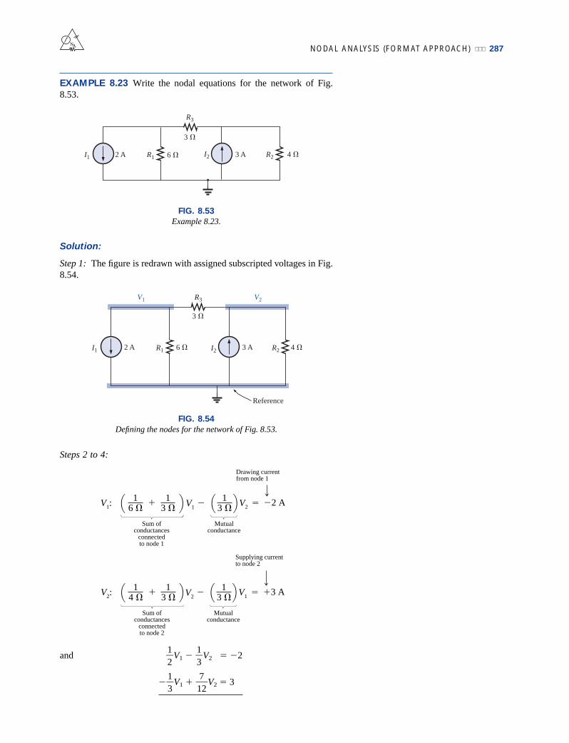
Steps 2 to 4:
and V1 V2 2
V1 V2 37
12
13
13
12
V2: V2 V11
4 1
3 1
3 3 A
Supplying currentto node 2
Sum ofconductances
connectedto node 2
Mutualconductance
V1: V1 V21
6 1
3 1
3 2 A
Drawing currentfrom node 1
Sum ofconductances
connectedto node 1
Mutualconductance
NA
2 A 6 R1 R2 4
R3
3 A
3
I2I1
FIG. 8.53
Example 8.23.
Reference
R1 6
R3
3
I2 3 A R2 4 I1 2 A
V1 V2
FIG. 8.54
Defining the nodes for the network of Fig. 8.53.
EXAMPLE 8.23 Write the nodal equations for the network of Fig.8.53.
Solution:
Step 1: The figure is redrawn with assigned subscripted voltages in Fig.8.54.

288 METHODS OF ANALYSIS AND SELECTED TOPICS (dc)
EXAMPLE 8.24 Find the voltage across the 3- resistor of Fig. 8.55by nodal analysis.
NA
2
V38 V–
+
6 10
4 3 1 V–
+
–
+
FIG. 8.55
Example 8.24.
FIG. 8.56
Defining the nodes for the network of Fig. 8.55.
V32
V1
4 A
–
+4 3
10 0.1 A
V2
Reference
6
V1 V2 4 A1
6
16
14
12
V2 V1 0.1 A
V1 V2 4
V1 V2 0.1
resulting in
11V1 2V2 485V1 18V2 3
and
11 485 3 33 240 207
V2 V3 ––––––––– –––––––––– –––– 1.101 V 11 2 198 10 1885 18
As demonstrated for mesh analysis, nodal analysis can also be a veryuseful technique for solving networks with only one source.
35
16
16
1112
16
16
13
110
Solution: Converting sources and choosing nodes (Fig. 8.56), wehave

NODAL ANALYSIS (FORMAT APPROACH) 289
EXAMPLE 8.25 Using nodal analysis, determine the potential acrossthe 4- resistor in Fig. 8.57.
Solution 1: The reference and four subscripted voltage levels werechosen as shown in Fig. 8.58. A moment of reflection should reveal thatfor any difference in potential between V1 and V3, the current throughand the potential drop across each 5- resistor will be the same. There-fore, V4 is simply a midvoltage level between V1 and V3 and is knownif V1 and V3 are available. We will therefore not include it in a nodalvoltage and will redraw the network as shown in Fig. 8.59. Understand,however, that V4 can be included if desired, although four nodal volt-ages will result rather than the three to be obtained in the solution ofthis problem.
V1: V1 V2 V3 01
10
12
110
12
12
NA
2
3 A
2
4 2
5 5
FIG. 8.57
Example 8.25.
2
3 A
2
4 2
5 5
V1
V4
V3V2
(0 V)
FIG. 8.58
Defining the nodes for the network of Fig.8.57.
2
3 A
2
4 2
V1
10
(0 V)
V2 V3
FIG. 8.59
Reducing the number of nodes for the networkof Fig. 8.57 by combining the two 5-
resistors.
V2: V2 V1 V3 3 A1
2
12
12
12
V3: V3 V2 V1 0
which are rewritten as
1.1V1 0.5V2 0.1V3 0V2 0.5V1 0.5V3 3
0.85V3 0.5V2 0.1V1 0
For determinants,
Before continuing, note the symmetry about the major diagonal inthe equation above. Recall a similar result for mesh analysis. Exam-ples 8.23 and 8.24 also exhibit this property in the resulting equations.Keep this thought in mind as a check on future applications of nodalanalysis.
1.1 0.5 0 0.5 1 3 0.1 0.5 0
V3 V4 ––––––––––––––––––– 4.645 V1.1 0.5 0.1 0.5 1 0.5 0.1 0.5 0.85
Mathcad Solution: By now the sequence of steps necessary tosolve a series of equations using Mathcad should be quite familiar andless threatening than the first encounter. For this example, all the param-eters were entered in the three simultaneous equations, avoiding the
1.1V1 0.5V2 0.1V3 0
0.1V1 0.5V2 0.85V3 0
0.5V1 1V2 0.5V3 3
c b a
b
a
110
12
14
12
110
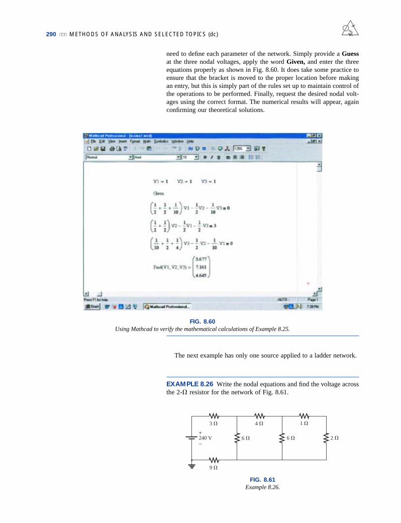
290 METHODS OF ANALYSIS AND SELECTED TOPICS (dc)
need to define each parameter of the network. Simply provide a Guessat the three nodal voltages, apply the word Given, and enter the threeequations properly as shown in Fig. 8.60. It does take some practice toensure that the bracket is moved to the proper location before makingan entry, but this is simply part of the rules set up to maintain control ofthe operations to be performed. Finally, request the desired nodal volt-ages using the correct format. The numerical results will appear, againconfirming our theoretical solutions.
NA
3 4 1
9
240 V 6 6 2 –
+
FIG. 8.61
Example 8.26.
FIG. 8.60
Using Mathcad to verify the mathematical calculations of Example 8.25.
The next example has only one source applied to a ladder network.
EXAMPLE 8.26 Write the nodal equations and find the voltage acrossthe 2- resistor for the network of Fig. 8.61.

BRIDGE NETWORKS 291
V1: V1 V2 0 20 V1
4
14
16
112
NA
FIG. 8.62
Converting the voltage source to a current source and defining the nodes for thenetwork of Fig. 8.61.
12
V1
2 20 A 6 6
(0 V)
1 4
V2 V3
Solution: The nodal voltages are chosen as shown in Fig. 8.62.
V2: V2 V1 V3 01
1
14
11
16
14
V3: V3 V2 0 0
and
0.5V1 0.25V2 0 20
0.25V1 V2 1V3 0
0 1V2 1.5V3 0
Note the symmetry present about the major axis. Application ofdeterminants reveals that
V3 V2 10.667 V
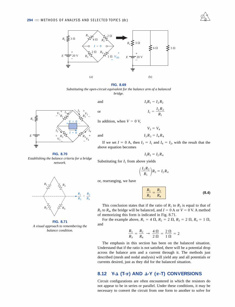
8.11 BRIDGE NETWORKS
This section introduces the bridge network, a configuration that has amultitude of applications. In the chapters to follow, it will be employedin both dc and ac meters. In the electronics courses it will be encoun-tered early in the discussion of rectifying circuits employed in convert-ing a varying signal to one of a steady nature (such as dc). A number ofother areas of application also require some knowledge of ac networks;these areas will be discussed later.
The bridge network may appear in one of the three forms as indi-cated in Fig. 8.63. The network of Fig. 8.63(c) is also called a symmet-rical lattice network if R2 R3 and R1 R4. Figure 8.63(c) is an excel-lent example of how a planar network can be made to appear nonplanar.For the purposes of investigation, let us examine the network of Fig.8.64 using mesh and nodal analysis.
1712
11
12
11

292 METHODS OF ANALYSIS AND SELECTED TOPICS (dc)
Mesh analysis (Fig. 8.65) yields
(3 4 2 )I1 (4 )I2 (2 )I3 20 V(4 5 2 )I2 (4 )I1 (5 )I3 0(2 5 1 )I3 (2 )I1 (5 )I2 0
and 009I1 4I2 2I3 204I1 11I2 5I3 02I1 5I2 8I3 0
with the result that
I1 4 A
I2 2.667 A
I3 2.667 A
The net current through the 5- resistor is
I5 I2 I3 2.667 A 2.667 A 0 A
Nodal analysis (Fig. 8.66) yields
V1 V2 V3 A203
12
14
12
14
13
NA
(b)
R2R1
R3 R4
R5
R1 R2
R5
R3 R4
(a) (c)
R2
R1
R3
R4
R5
FIG. 8.63
Various formats for a bridge network.
FIG. 8.64
Standard bridge configuration.
Rs 3 R2
2
R3
2 5
R5
1
R4
4
R1
E 20 V
Rs 3 R22
R3 1
R1
E 20 V
I1
4 R5 I2
I35 2 R4
FIG. 8.65
Assigning the mesh currents to the network of Fig. 8.64.
R1
R2R5
R3
R4
2
3 I Rs
V2
V1
V3
4
5 2
1
203 A
(0 V)
FIG. 8.66
Defining the nodal voltages for the network of Fig. 8.64.
det[[20/3,1/4,1/2][0,(1/41/21/5),1/5][0,1/5,(1/51/21/1)]] ENTER 10.5
CALC. 8.4
V2 V1 V3 01
5
14
15
12
14
V3 V1 V2 0
and
V1 V2 V3 A203
12
14
12
14
13
15
12
11
12
15
V1 V2 V3 01
5
15
12
14
14
V1 V2 V3 0
Note the symmetry of the solution.With the TI-86 calculator, the top part of the determinant is determined
by the following (take note of the calculations within parentheses):
11
12
15
15
12

BRIDGE NETWORKS 293NA
with the bottom of the determinant determined by:
det[[(1/31/41/2),1/4,1/2][1/4,(1/41/21/5),1/5][1/2,1/5,(1/51/21/1)]] ENTER 1.312
CALC. 8.5
Finally, 10.5/1.312 ENTER 8
CALC. 8.6
and V1 8 V
Similarly, V2 2.667 V and V3 2.667 V
and the voltage across the 5- resistor is
V5 V2 V3 2.667 V 2.667 V 0 V
Since V5 0 V, we can insert a short in place of the bridge arm with-out affecting the network behavior. (Certainly V IR I·(0) 0 V.) In Fig. 8.67, a short circuit has replaced the resistor R5, and the volt-age across R4 is to be determined. The network is redrawn in Fig. 8.68, and
V1 (voltage divider rule)
2.667 V
as obtained earlier.We found through mesh analysis that I5 0 A, which has as its
equivalent an open circuit as shown in Fig. 8.69(a). (Certainly I V/R 0/(∞ ) 0 A.) The voltage across the resistor R4 will againbe determined and compared with the result above.
The network is redrawn after combining series elements, as shown inFig. 8.69(b), and
V3 8 V
and V1 2.667 V
as above.The condition V5 0 V or I5 0 A exists only for a particular
relationship between the resistors of the network. Let us now derive thisrelationship using the network of Fig. 8.70, in which it is indicated thatI 0 A and V 0 V. Note that resistor Rs of the network of Fig. 8.69will not appear in the following analysis.
The bridge network is said to be balanced when the condition ofI 0 A or V 0 V exists.
If V 0 V (short circuit between a and b), then
V1 V2
8 V
31 (8 V)1 2
2 (20 V)2 3
(6 3 )(20 V)6 3 3
40 V
152(20 V)
2 4 9
23
(20 V)23
43
93
23
(20 V)23
86
3
(2 1 )20 V(2 1 ) (4 2 ) 3
R1
R2
R3
R4
2
E
4
2
1
V = 0
Rs 3
20 V
–
+V1
FIG. 8.67
Substituting the short-circuit equivalent forthe balance arm of a balanced bridge.
R1 2
–
+
4 R2
R3 1 2 R4
Rs 3
E 20 V V1–
+
FIG. 8.68
Redrawing the network of Fig. 8.67.
294 METHODS OF ANALYSIS AND SELECTED TOPICS (dc)
and I1R1 I2 R2
or I1
In addition, when V 0 V,
V3 V4
and I3 R3 I4 R4
If we set I 0 A, then I3 I1 and I4 I2, with the result that theabove equation becomes
I1R3 I2 R4
Substituting for I1 from above yields
R3 I2 R4
or, rearranging, we have
(8.4)
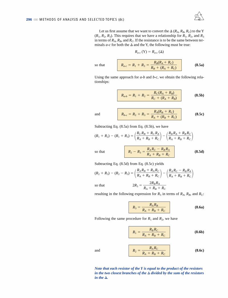
This conclusion states that if the ratio of R1 to R3 is equal to that ofR2 to R4, the bridge will be balanced, and I 0 A or V 0 V. A methodof memorizing this form is indicated in Fig. 8.71.
For the example above, R1 4 , R2 2 , R3 2 , R4 1 ,and
2
The emphasis in this section has been on the balanced situation.Understand that if the ratio is not satisfied, there will be a potential dropacross the balance arm and a current through it. The methods justdescribed (mesh and nodal analysis) will yield any and all potentials orcurrents desired, just as they did for the balanced situation.
8.12 Y-D (T-p) AND D-Y (p-T) CONVERSIONS
Circuit configurations are often encountered in which the resistors donot appear to be in series or parallel. Under these conditions, it may benecessary to convert the circuit from one form to another to solve for
2 1
4 2
R2R4
R1R3
R
R1
3
R
R2
4
I2 R2
R1
I2 R2
R1
NA
R1
R2
R3
R4
2
E
4
2
1
Rs 3
20 V–
+
–
+
I = 0
(a)
V1
6
3 Rs
3
E 20 V–
+
(b)
FIG. 8.69
Substituting the open-circuit equivalent for the balance arm of a balanced bridge.
R1
R3E
V = 0Rs
–
+I = 0
R4V4
I4
I1V1–+ I2
V2–
+R2
V3 –
+
I3
–+
FIG. 8.70
Establishing the balance criteria for a bridge network.
R1
R3
R2
R4
R1
R3
R2
R4=
FIG. 8.71
A visual approach to remembering thebalance condition.
NA Y-D (T-p) AND D-Y (p-T) CONVERSIONS 295
any unknown quantities if mesh or nodal analysis is not applied. Twocircuit configurations that often account for these difficulties are thewye (Y) and delta () configurations, depicted in Fig. 8.72(a). Theyare also referred to as the tee (T) and pi (), respectively, as indicatedin Fig. 8.72(b). Note that the pi is actually an inverted delta.
RB
RC
RA
“ ”
R1 R2
R3
“ ”
RB RA
RC
“ ”
(a) (b)
R1 R2
R3
“ ”
FIG. 8.72
The Y (T) and D (p) configurations.
The purpose of this section is to develop the equations for convert-ing from D to Y, or vice versa. This type of conversion will normallylead to a network that can be solved using techniques such as thosedescribed in Chapter 7. In other words, in Fig. 8.73, with terminals a,b, and c held fast, if the wye (Y) configuration were desired instead ofthe inverted delta (D) configuration, all that would be necessary is adirect application of the equations to be derived. The phrase instead ofis emphasized to ensure that it is understood that only one of these con-figurations is to appear at one time between the indicated terminals.
It is our purpose (referring to Fig. 8.73) to find some expression forR1, R2, and R3 in terms of RA, RB, and RC, and vice versa, that willensure that the resistance between any two terminals of the Y configu-ration will be the same with the D configuration inserted in place of theY configuration (and vice versa). If the two circuits are to be equivalent,the total resistance between any two terminals must be the same. Con-sider terminals a-c in the D-Y configurations of Fig. 8.74.
a
RARBR3
R2R1
RCb
c
“ ”
FIG. 8.73
Introducing the concept of D-Y or Y-Dconversions.
R1 R2
R3
a b
c
Ra-c RB RA
RC
a b
c
Ra-c
RB RA
RC
a
b
c
Ra-c
External to pathof measurement
FIG. 8.74
Finding the resistance Ra-c for the Y and D configurations.
296 METHODS OF ANALYSIS AND SELECTED TOPICS (dc)
Let us first assume that we want to convert the D (RA, RB, RC) to the Y(R1, R2, R3). This requires that we have a relationship for R1, R2, and R3
in terms of RA, RB, and RC. If the resistance is to be the same between ter-minals a-c for both the D and the Y, the following must be true:
Ra-c (Y) Ra-c (D)
so that (8.5a)
Using the same approach for a-b and b-c, we obtain the following rela-tionships:
(8.5b)
and (8.5c)
Subtracting Eq. (8.5a) from Eq. (8.5b), we have
(R1 R2) (R1 R3)
so that (8.5d)
Subtracting Eq. (8.5d) from Eq. (8.5c) yields
(R2 R3) (R2 R3) so that 2R3
RA
2RRB
B
RA
RC
resulting in the following expression for R3 in terms of RA, RB, and RC:
(8.6a)
Following the same procedure for R1 and R2, we have
(8.6b)
and (8.6c)
Note that each resistor of the Y is equal to the product of the resistorsin the two closest branches of the D divided by the sum of the resistorsin the D.
R2 RA
R
RA R
B
C
RC
R1 RA
R
RB R
B
C
RC
R3 RA
R
RA
B
RB
RC
RA RC RB RARA RB RC
RA RB RA RCRA RB RC
R2 R3 R
R
A
A R
C
R
B
R
B R
RA
C
RB RA RB RCRA RB RC
RC RB RC RARA RB RC
Rb-c R2 R3 RA
RA
(R
(B
RB
RC
R
)
C)
Ra-b R1 R2 RC
RC
(R
(A
RA
RB
R
)
B)
Ra-c R1 R3 RB
R
B(R
(A
RA
RC
R
)
C)
NA

Y-D (T-p) AND D-Y (p-T) CONVERSIONS 297
To obtain the relationships necessary to convert from a Y to a D, firstdivide Eq. (8.6a) by Eq. (8.6b):
RR
C
A
or RA
Then divide Eq. (8.6a) by Eq. (8.6c):
RR
C
B
or RB
Substituting for RA and RB in Eq. (8.6c) yields
R2
Placing these over a common denominator, we obtain
R2
and RC (8.7a)
We follow the same procedure for RB and RA:
RA (8.7b)
and RB (8.7c)
Note that the value of each resistor of the D is equal to the sum of thepossible product combinations of the resistances of the Y divided bythe resistance of the Y farthest from the resistor to be determined.
Let us consider what would occur if all the values of a D or Ywere the same. If RA RB RC, Equation (8.6a) would become(using RA only) the following:
R3 RA
RRAR
B
B
RC
RA
RRAR
A
A
RA
3RR
2A
A
and, following the same procedure,
R1 R2 RA3
RA3
RA3
R1R2 R1R3 R2R3
R2
R1R2 R1R3 R2R3
R1
R1R2 R1R3 R2R3
R3
R2R3RCR1R2 R1R3 R2R3
(R3RC /R1)(R1R2 R1R3 R2R3)/(R1R2)
(R3 /R1)RC(R3 /R2) (R3 /R1) 1
(RC R3 /R1)RC(R3 RC /R2) (RC R3 /R1) RC
R3 RC
R2
(RARB)/(RA RB RC)(RARC)/(RA RB RC)
R3R2
RC R3
R1
(RA RB) /(RA RB RC)(RB RC) /(RA RB RC)
R3R1
NA

298 METHODS OF ANALYSIS AND SELECTED TOPICS (dc)
In general, therefore,
(8.8a)
or (8.8b)
which indicates that for a Y of three equal resistors, the value of eachresistor of the D is equal to three times the value of any resistor of theY. If only two elements of a Y or a D are the same, the correspondingD or Y of each will also have two equal elements. The converting ofequations will be left as an exercise for the reader.
The Y and the D will often appear as shown in Fig. 8.75. They arethen referred to as a tee (T) and a pi () network, respectively. Theequations used to convert from one form to the other are exactly thesame as those developed for the Y and D transformation.
RD 3RY
RY R
3D
NA
(a)
R1
1
2
3
4
R2
R3
“ ” “ ” “ ”
RC
1
2
3
4
RB RA
“ ”
(b)
FIG. 8.75
The relationship between the Y and T configurations and the D and pconfigurations.
EXAMPLE 8.27 Convert the D of Fig. 8.76 to a Y.
RB
RA
RCab
c
a
b
c
20 30
10
FIG. 8.76
Example 8.27.
R3 10
R1
31/3 R2
5
aba
b
cc
FIG. 8.77
The Y equivalent for the D of Fig. 8.76.
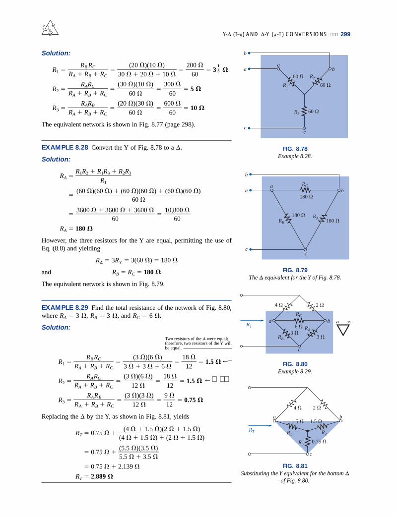
Solution:
R1 3
R2 5
R3 10
The equivalent network is shown in Fig. 8.77 (page 298).
EXAMPLE 8.28 Convert the Y of Fig. 8.78 to a D.
Solution:
RA
RA 180
However, the three resistors for the Y are equal, permitting the use ofEq. (8.8) and yielding
RD 3RY 3(60 ) 180
and RB RC 180
The equivalent network is shown in Fig. 8.79.
EXAMPLE 8.29 Find the total resistance of the network of Fig. 8.80,where RA 3 , RB 3 , and RC 6 .
Solution:
Two resistors of the D were equal;therefore, two resistors of the Y willbe equal.
R1 1.5
R2 1.5
R3 0.75
Replacing the D by the Y, as shown in Fig. 8.81, yields
RT 0.75
0.75
0.75 2.139
RT 2.889
(5.5 )(3.5 )5.5 3.5
(4 1.5 )(2 1.5 )(4 1.5 ) (2 1.5 )
9 12
(3 )(3 )
12
RARBRA RB RC
18
12
(3 )(6 )
12
RARCRA RB RC
18
12
(3 )(6 )3 3 6
RBRCRA RB RC
10,800
603600 3600 3600
60
(60 )(60 ) (60 )(60 ) (60 )(60 )
60
R1R2 R1R3 R2R3
R1
600
60
(20 )(30 )
60
RARBRA RB RC
300
60
(30 )(10 )
60 RARC
RA RB RC
13
200
60
(20 )(10 )30 20 10
RB RCRA RB RC
←−
Y-D (T-p) AND D-Y (p-T) CONVERSIONS 299NA
R3 60
R1
60 R2
60
aba
b
cc
FIG. 8.78
Example 8.28.
RC
RB
180 RA
aba
b
cc
180
180
FIG. 8.79
The D equivalent for the Y of Fig. 8.78.
RB
3 RA
3
ba
c
4 2
6 “ ”RT
RC
FIG. 8.80
Example 8.29.
RT
0.75
R1
ba
c
4 2
1.5 1.5
R3
R2
FIG. 8.81
Substituting the Y equivalent for the bottom Dof Fig. 8.80.
←
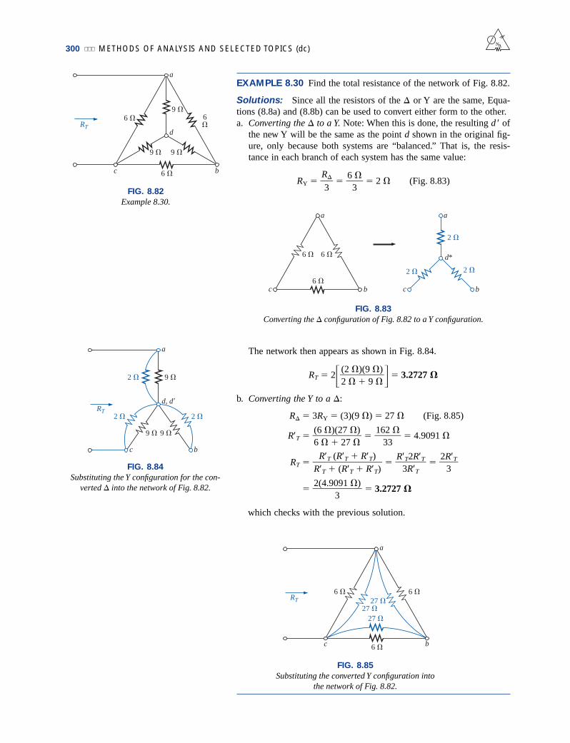
300 METHODS OF ANALYSIS AND SELECTED TOPICS (dc)
EXAMPLE 8.30 Find the total resistance of the network of Fig. 8.82.
Solutions: Since all the resistors of the D or Y are the same, Equa-tions (8.8a) and (8.8b) can be used to convert either form to the other.a. Converting the D to a Y. Note: When this is done, the resulting d ′ of
the new Y will be the same as the point d shown in the original fig-ure, only because both systems are “balanced.” That is, the resis-tance in each branch of each system has the same value:
RY 2 (Fig. 8.83)6
3
RD3
NA
FIG. 8.82
Example 8.30.
RT
6
a
bc
9 6
9 9
6
d
d*
2
2 2
a
bc
6
a
bc
6
6
FIG. 8.83
Converting the D configuration of Fig. 8.82 to a Y configuration.
RT
9
a
2
d, d
c b
9 9
2 2
FIG. 8.84
Substituting the Y configuration for the con-verted D into the network of Fig. 8.82.
RT6
a
bc
27 6
6
27 27
FIG. 8.85
Substituting the converted Y configuration intothe network of Fig. 8.82.
The network then appears as shown in Fig. 8.84.
RT 2 3.2727
b. Converting the Y to a D:
RD 3RY (3)(9 ) 27 (Fig. 8.85)
R′T 4.9091
RT
3.2727
which checks with the previous solution.
2(4.9091 )
3
2R′T3
R′T2R′T3R′T
R′T (R′T R′T)R′T (R′T R′T)
162
33(6 )(27 )6 27
(2 )(9 )2 9

APPLICATIONS 301NA
8.13 APPLICATIONS
The Applications section of this chapter will discuss the constant cur-rent characteristic in the design of security systems, the bridge circuit ina common residential smoke detector, and the nodal voltages of a digi-tal logic probe.
Constant Current Alarm Systems
The basic components of an alarm system employing a constant currentsupply are provided in Fig. 8.86. This design is improved over that pro-vided in Chapter 5 in the sense that it is less sensitive to changes inresistance in the circuit due to heating, humidity, changes in the lengthof the line to the sensors, and so on. The 1.5-k rheostat (total resis-tance between points a and b) is adjusted to ensure a current of 5 mAthrough the single-series security circuit. The adjustable rheostat is nec-essary to compensate for variations in the total resistance of the circuitintroduced by the resistance of the wire, sensors, sensing relay, and mil-liammeter. The milliammeter is included to set the rheostat and ensurea current of 5 mA.
Magneticswitch
Windowfoil
Doorswitch
Sensing relay
1 kΩ
≅ 5 mA
E 10 V+
–
Rheostat0 1.5 kΩ
10-mAmovement
N/C
N/O 5 V @ 5 mA
To bell circuit
1 kΩ
a
b
FIG. 8.86
Constant current alarm system.
If any of the sensors should open, the current through the entire cir-cuit will drop to zero, the coil of the relay will release the plunger, andcontact will be made with the N/C position of the relay. This action willcomplete the circuit for the bell circuit, and the alarm will sound. Forthe future, keep in mind that switch positions for a relay are alwaysshown with no power to the network, resulting in the N/C position ofFig. 8.86. When power is applied, the switch will have the position indi-cated by the dashed line. That is, various factors, such as a change inresistance of any of the elements due to heating, humidity, and so on,would cause the applied voltage to redistribute itself and create a sensi-tive situation. With an adjusted 5 mA, the loading can change, but thecurrent will always be 5 mA and the chance of tripping reduced. Takenote of the fact that the relay is rated as 5 V at 5 mA, indicating that inthe on state the voltage across the relay is 5 V and the current throughthe relay 5 mA. Its internal resistance is therefore 5 V/5 mA 1 k inthis state.
A more advanced alarm system using a constant current is providedin Fig. 8.87. In this case an electronic system employing a single tran-
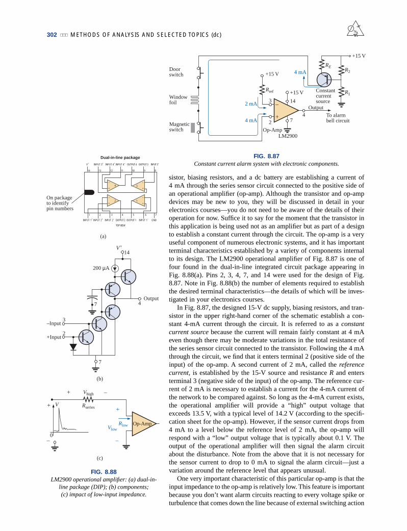
302 METHODS OF ANALYSIS AND SELECTED TOPICS (dc)
sistor, biasing resistors, and a dc battery are establishing a current of4 mA through the series sensor circuit connected to the positive side ofan operational amplifier (op-amp). Although the transistor and op-ampdevices may be new to you, they will be discussed in detail in yourelectronics courses—you do not need to be aware of the details of theiroperation for now. Suffice it to say for the moment that the transistor inthis application is being used not as an amplifier but as part of a designto establish a constant current through the circuit. The op-amp is a veryuseful component of numerous electronic systems, and it has importantterminal characteristics established by a variety of components internalto its design. The LM2900 operational amplifier of Fig. 8.87 is one offour found in the dual-in-line integrated circuit package appearing inFig. 8.88(a). Pins 2, 3, 4, 7, and 14 were used for the design of Fig.8.87. Note in Fig. 8.88(b) the number of elements required to establishthe desired terminal characteristics—the details of which will be inves-tigated in your electronics courses.
In Fig. 8.87, the designed 15-V dc supply, biasing resistors, and tran-sistor in the upper right-hand corner of the schematic establish a con-stant 4-mA current through the circuit. It is referred to as a constantcurrent source because the current will remain fairly constant at 4 mAeven though there may be moderate variations in the total resistance ofthe series sensor circuit connected to the transistor. Following the 4 mAthrough the circuit, we find that it enters terminal 2 (positive side of theinput) of the op-amp. A second current of 2 mA, called the referencecurrent, is established by the 15-V source and resistance R and entersterminal 3 (negative side of the input) of the op-amp. The reference cur-rent of 2 mA is necessary to establish a current for the 4-mA current ofthe network to be compared against. So long as the 4-mA current exists,the operational amplifier will provide a “high” output voltage thatexceeds 13.5 V, with a typical level of 14.2 V (according to the specifi-cation sheet for the op-amp). However, if the sensor current drops from4 mA to a level below the reference level of 2 mA, the op-amp willrespond with a “low” output voltage that is typically about 0.1 V. Theoutput of the operational amplifier will then signal the alarm circuitabout the disturbance. Note from the above that it is not necessary forthe sensor current to drop to 0 mA to signal the alarm circuit—just avariation around the reference level that appears unusual.
One very important characteristic of this particular op-amp is that theinput impedance to the op-amp is relatively low. This feature is importantbecause you don’t want alarm circuits reacting to every voltage spike orturbulence that comes down the line because of external switching action
NA
Magneticswitch
Windowfoil
Doorswitch
2 mA
4 mA
+15 V
Rref
3
2
+15 V
+
–
LM2900
14
74
Output
Constantcurrentsource
To alarmbell circuit
+15 V
4 mARE
R2
R1
Op-Amp
FIG. 8.87
Constant current alarm system with electronic components.
(a)
V+
14
200 µA
4Output
–Input
+Input
3
2
7
(b)
+ Vhigh –
+
–
RseriesV
+
–0
VlowRlow Op-Amp
(c)
7
INPUT 3+
On packageto identifypin numbers
Dual-in-line package
V+ INPUT 4+ INPUT 4– OUTPUT 4 OUTPUT 3 INPUT 3–
14 13 12 11 10 9 8
4–
+
2–
+
–
+
–
+
3
1
1 2 3 4 5 6 7
INPUT 1+ INPUT 2+ INPUT 2– OUTPUT 2 GNDOUTPUT 1 INPUT 1–
TOP VIEW
FIG. 8.88
LM2900 operational amplifier: (a) dual-in-line package (DIP); (b) components; (c) impact of low-input impedance.

APPLICATIONS 303
or outside forces such as lightning. In Fig. 8.88(c), for instance, if a highvoltage should appear at the input to the series configuration, most of thevoltage will be absorbed by the series resistance of the sensor circuitrather than traveling across the input terminals of the operational ampli-fier—thus preventing a false output and an activation of the alarm.
Wheatstone Bridge Smoke Detector
TheWheatstonebridgeisapopularnetworkconfigurationwheneverdetec-tion of small changes in a quantity is required. In Fig. 8.89(a), the dc bridgeconfiguration is employing a photoelectric device to detect the presence ofsmoke and to sound the alarm. A photograph of an actual photoelectricsmoke detector appears in Fig. 8.89(b), and the internal construction of theunit is shown in Fig. 8.89(c). First note that air vents are provided to permitthesmoketoenter thechamberbelowtheclearplastic.Theclearplasticwillprevent thesmokefromentering theupperchamberbutwillpermit the light
NA
(a)
Balanceadjust
Rbalance
Reference
Sensitiverelay
Vbalance+ –
Smokedetector
R
Lamp
N/C
N/O
To alarm circuit
+
–
DCpower
a b
FIG. 8.89(a)(b)
Wheatstone bridge detector: (a) dc bridge configuration; (b) outside appearance.

304
from the bulb in the upper chamber to bounce off the lower reflector to thesemiconductor light sensor (a cadmium photocell) at the left side of thechamber. The clear plastic separation ensures that the light hitting the lightsensor in the upper chamber is not affected by the entering smoke. It estab-lishes a reference level to compare against the chamber with the enteringsmoke. If no smoke is present, the difference in response between the sen-sor cells will be registered as the normal situation. Of course, if both cellswere exactly identical, and if the clear plastic did not cut down on the light,both sensors would establish the same reference level, and their differencewould be zero. However, this is seldom the case, so a reference difference isrecognized as the sign that smoke is not present. However, once smoke ispresent, there will be a sharp difference in the sensor reaction from thenorm, and the alarm should be sounded.
In Fig. 8.89(a), we find that the two sensors are located on oppositearms of the bridge. With no smoke present the balance-adjust rheostat willbe used to ensure that the voltage V between points a and b is zero volts andthe resulting current through the primary of the sensitive relay will be zeroamperes. Taking a look at the relay, we find that the absence of a voltagefrom a to b will leave the relay coil unenergized and the switch in the N/Oposition (recall that the position of a relay switch is always drawn in theunenergized state). An unbalanced situation will result in a voltage acrossthe coil and activation of the relay, and the switch will move to the N/Cposition to complete the alarm circuit and activate the alarm. Relays withtwo contacts and one movable arm are called single-pole–double-throw(SPDT) relays. The dc power is required to set up the balance situation,energize the parallel bulb so we know that the system is on, and provide thevoltage from a to b if an unbalanced situation should develop.
One may ask why only one sensor isn’t used since its resistancewould be sensitive to the presence of smoke. The answer lies in the factthat the smoke detector might generate a false readout if the supplyvoltage or output light intensity of the bulb should vary. Smoke detec-tors of the type just described must be used in gas stations, kitchens,dentist offices, etc., where the range of gas fumes present may set off anionizing type smoke detector.
Ceiling Reflector
Reference cell
Sealed chamber
Solid barrier
Lightsource
Clearplastic
Reflector
Vents for thepassage of air or smoke
Room
Smokedetector
Photoconductivecells
(Resistance a functionof applied light)
(c)
FIG. 8.89(c)
Wheatstone bridge smoke detector: (c) internal construction.

APPLICATIONS 305
Schematic with Nodal Voltages
When an investigator is presented with a system that is down or notoperating properly, one of the first options is to check the system’sspecified voltages on the schematic. These specified voltage levels areactually the nodal voltages determined in this chapter. Nodal voltage issimply a special term for a voltage measured from that point to ground.The technician will attach the negative or lower-potential lead to theground of the network (often the chassis) and then place the positive orhigher-potential lead on the specified points of the network to check thenodal voltages. If they match, it is a good sign that that section of thesystem is operating properly. If one or more fail to match the given val-ues, the problem area can usually be identified. Be aware that a readingof 15.87 V is significantly different from an expected reading of16 V if the leads have been properly attached. Although the actualnumbers seem close, the difference is actually more than 30 V. Onemust expect some deviation from the given value as shown, but alwaysbe very sensitive to the resulting sign of the reading.
The schematic of Fig. 8.90(a) includes the nodal voltages for a logicprobe used to measure the input and output states of integrated circuitlogic chips. In other words, the probe determines whether the measuredvoltage is one of two states: high or low (often referred to as “on” or“off” or 1 or 0). If the LOGIC IN terminal of the probe is placed on achip at a location where the voltage is between 0 and 1.2 V, the voltageis considered a low level, and the green LED will light. (LEDs are light-emitting semiconductor diodes that will emit light when current ispassed through them.) If the measured voltage is between 1.8 V and5 V, the reading is considered high, and the red LED will light. Anyvoltage between 1.2 V and 1.8 V is considered a “floating level” and isan indication that the system being measured is not operating correctly.Note that the reference levels mentioned above are established by thevoltage divider network to the right of the schematic. The op-ampsemployed are of such high input impedance that their loading on thevoltage divider network can be ignored and the voltage divider networkconsidered a network unto itself. Even though three 5.5-V dc supplyvoltages are indicated on the diagram, be aware that all three points areconnected to the same supply. The other voltages provided (the nodalvoltages) are the voltage levels that should be present from that point toground if the system is working properly.
The op-amps are used to sense the difference between the referenceat points 3 and 6 and the voltage picked up in LOGIC IN. Any differ-ence will result in an output that will light either the green or the redLED. Be aware, because of the direct connection, that the voltage atpoint 3 is the same as shown by the nodal voltage to the left, or 1.8 V.Likewise, the voltage at point 6 is 1.2 V for comparison with the volt-ages at points 5 and 2, which reflect the measured voltage. If the inputvoltage happened to be 1.0 V, the difference between the voltages atpoints 5 and 6 would be 0.2 V, which ideally would appear at point 7.This low potential at point 7 would result in a current flowing from themuch higher 5.5-V dc supply through the green LED, causing it to lightand indicating a low condition. By the way, LEDs, like diodes, permitcurrent through them only in the direction of the arrow in the symbol.Also note that the voltage at point 6 must be higher than that at point 5for the output to turn on the LED. The same is true for point 2 overpoint 3, which reveals why the red LED does not light when the 1.0-Vlevel is measured.
NA
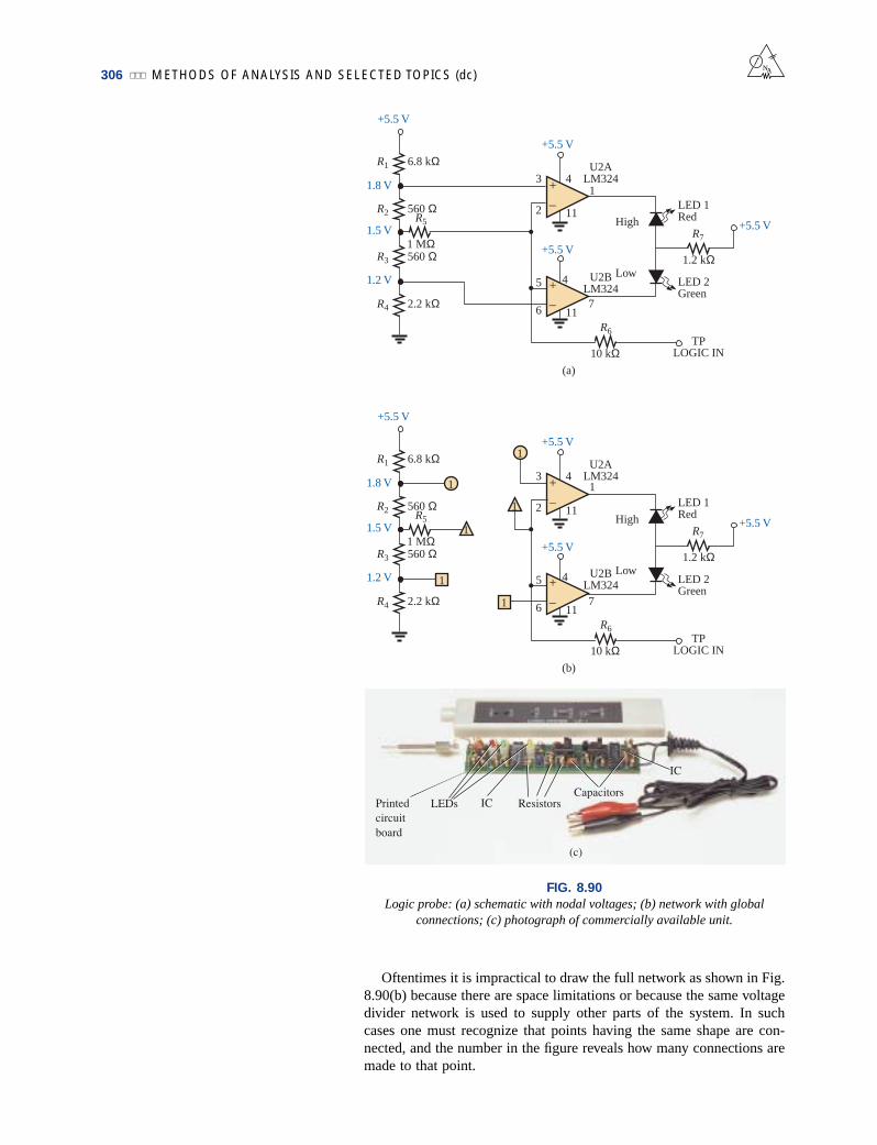
306 METHODS OF ANALYSIS AND SELECTED TOPICS (dc)
Oftentimes it is impractical to draw the full network as shown in Fig.8.90(b) because there are space limitations or because the same voltagedivider network is used to supply other parts of the system. In suchcases one must recognize that points having the same shape are con-nected, and the number in the figure reveals how many connections aremade to that point.
NA
FIG. 8.90
Logic probe: (a) schematic with nodal voltages; (b) network with globalconnections; (c) photograph of commercially available unit.
–
+
–
+
+5.5 V
R1 6.8 kΩ
1.8 V
1.5 V
1.2 V
R2 560 Ω
R3 560 Ω
R4 2.2 kΩ
R5
1 MΩ
3 4
2 11
4
117
+5.5 V
+5.5 V
U2ALM324
5
6
High
Low
R6
10 kΩTP
LOGIC IN
LED 1Red
LED 2Green
+5.5 VR7
1.2 kΩ
(b)
1
1
1
1
1
1
–
+
–
+
+5.5 V
R1 6.8 kΩ
1.8 V
1.5 V
1.2 V
R2 560 Ω
R3 560 Ω
R4 2.2 kΩ
R5
1 MΩ
3 4
2 11
4
117
+5.5 V
+5.5 V
U2ALM324
5
6
High
Low
R6
10 kΩTP
LOGIC IN
LED 1Red
LED 2Green
+5.5 VR7
1.2 kΩ
(a)
U2BLM324
1
1
U2BLM324

A photograph of the outside and inside of a commercially avail-able logic probe is provided in Fig. 8.90(c). Note the increasedcomplexity of system because of the variety of functions that the probecan perform.
8.14 COMPUTER ANALYSIS
PSpice
The bridge network of Fig. 8.70 will now be analyzed using PSpice toensure that it is in the balanced state. The only component that has notbeen introduced in earlier chapters is the dc current source. It can beobtained by first selecting the Place a part key and then the SOURCElibrary. Scrolling the Part List will result in the option IDC. A leftclick of IDC followed by OK will result in a dc current source whosedirection is toward the bottom of the screen. One left click of the mouse(to make it red—active) followed by a right click of the mouse willresult in a listing having a Mirror Vertically option. Selecting thatoption will flip the source and give it the direction of Fig. 8.70.
The remaining parts of the PSpice analysis are pretty straightfor-ward, with the results of Fig. 8.91 matching those obtained in the analy-sis of Fig. 8.70. The voltage across the current source is 8 V positive toground, and the voltage at either end of the bridge arm is 2.667 V. Thevoltage across R5 is obviously 0 V for the level of accuracy displayed,and the current is of such a small magnitude compared to the other cur-rent levels of the network that it can essentially be considered 0 A. Notealso for the balanced bridge that the current through R1 equals that ofR3, and the current through R2 equals that of R4.
NA COMPUTER ANALYSIS 307
FIG. 8.91
Applying PSpice to the bridge network of Fig. 8.70.

For the analysis, both indicators and a meter will be used to displaythe desired results. An A indicator in the H position was used for thecurrent through R5, and a V indicator in the V position was used for thevoltage across R2. A multimeter in the voltmeter mode was placed toread the voltage across R4. The ammeter is reading the mesh or loopcurrent for that branch, and the two voltmeters are displaying the nodalvoltages of the network.
After simulation, the results displayed are an exact match with thoseof Example 8.18.
308 METHODS OF ANALYSIS AND SELECTED TOPICS (dc)
Electronics Workbench
Electronics Workbench will now be used to verify the results of Exam-ple 8.18. All the elements of creating the schematic of Fig. 8.92 havebeen presented in earlier chapters; they will not be repeated here inorder to demonstrate how little documentation is now necessary to carryyou through a fairly complex network.
NA
FIG. 8.92
Using Electronics Workbench to verify the results of Example 8.18.
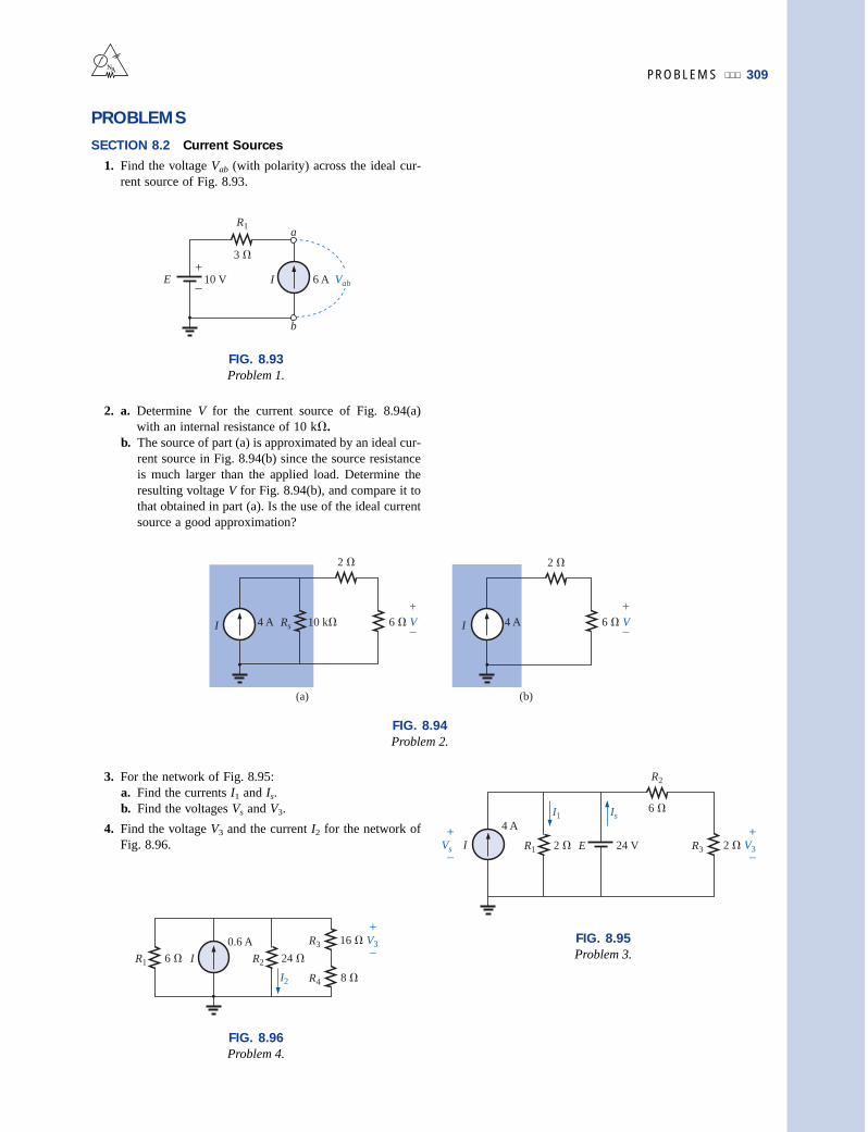
NA PROBLEMS 309
R1
E VabI 6 A
3
a
b
+
–10 V
FIG. 8.93
Problem 1.
Rs 10 k
2
4 AI 6 V+
–
(a)
2
4 AI 6 V+
–
(b)
FIG. 8.94
Problem 2.
2. a. Determine V for the current source of Fig. 8.94(a)with an internal resistance of 10 k.
b. The source of part (a) is approximated by an ideal cur-rent source in Fig. 8.94(b) since the source resistanceis much larger than the applied load. Determine theresulting voltage V for Fig. 8.94(b), and compare it tothat obtained in part (a). Is the use of the ideal currentsource a good approximation?
PROBLEMS
SECTION 8.2 Current Sources
1. Find the voltage Vab (with polarity) across the ideal cur-rent source of Fig. 8.93.
3. For the network of Fig. 8.95:a. Find the currents I1 and Is.b. Find the voltages Vs and V3.
4. Find the voltage V3 and the current I2 for the network ofFig. 8.96.
FIG. 8.95
Problem 3.
R1 2
6
4 A
I 2 V3
+
–
R2
R3E 24 VVs
+
–
I1 Is
FIG. 8.96
Problem 4.
R1 6
0.6 A
I
16 V3
+
–R3
I2
R2 24
8 R4

SECTION 8.3 Source Conversions
5. Convert the voltage sources of Fig. 8.97 to currentsources.
310 METHODS OF ANALYSIS AND SELECTED TOPICS (dc)NA
E 18 V
(a)
Rs
6
E 9 V
(b)
Rs
2.2 k
FIG. 8.97
Problem 5.
6. Convert the current sources of Fig. 8.98 to voltagesources.
Rs3
1.5 A
(a)
Rs
4.7 k
6 mA
(b)
II
FIG. 8.98
Problem 6.
FIG. 8.99
Problem 7.
Rs 4 12 A
I RL 2
FIG. 8.100
Problem 8.
R1
10
R2
6.8
R3 39 E 12 V
I1
Vab
a
b
I = 2 A
7. For the network of Fig. 8.99:a. Find the current through the 2- resistor.b. Convert the current source and 4- resistor to a volt-
age source, and again solve for the current in the 2-resistor. Compare the results.
8. For the configuration of Fig. 8.100:a. Convert the current source and 6.8- resistor to a
voltage source.b. Find the magnitude and direction of the current I1.c. Find the voltage Vab and the polarity of points a and b.

PROBLEMS 311NA
SECTION 8.4 Current Sources in Parallel
9. Find the voltage V2 and the current I1 for the network ofFig. 8.101.
10. a. Convert the voltage sources of Fig. 8.102 to currentsources.
b. Find the voltage Vab and the polarity of points a and b.c. Find the magnitude and direction of the current I.
FIG. 8.101
Problem 9.
7 A
I1
V2R1 4 R2 6 3 A
+
–
FIG. 8.102
Problem 10.
R1 3
E1 9 V
R2 2
E2 20 V
R3 6 R412
I
b
a
Vab
FIG. 8.103
Problem 11.
V2
R1 6.8 k 12 V
+ –R2
2.2 k
I2
3 mA
8 mA
V1
+
–
FIG. 8.104
Problems 12, 17, 25, and 54.
R3 8 6 V
R2
2
E2
R1
4
4 V E1
R2 3
10 VE1
R1 4
12 VE2
R3 12
(a) (b)
11. For the network of Fig. 8.103:a. Convert the voltage source to a current source.b. Reduce the network to a single current source, and
determine the voltage V1.c. Using the results of part (b), determine V2.d. Calculate the current I2.
SECTION 8.6 Branch-Current Analysis
12. Using branch-current analysis, find the magnitude anddirection of the current through each resistor for the net-works of Fig. 8.104.
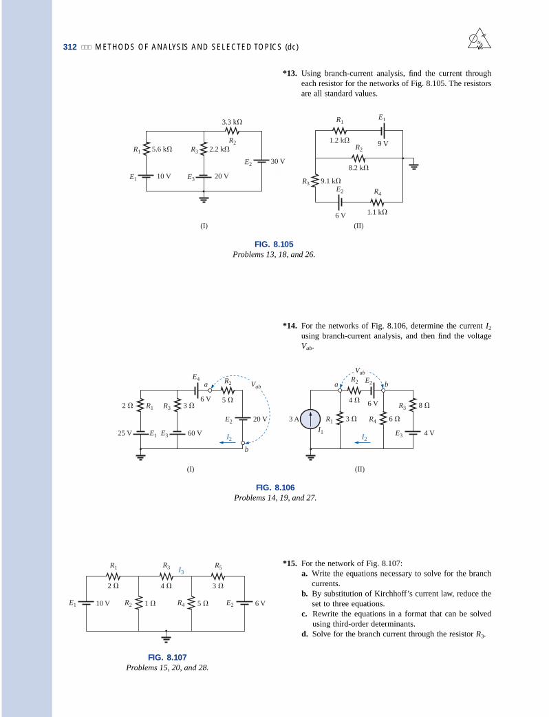
312 METHODS OF ANALYSIS AND SELECTED TOPICS (dc)NA
*13. Using branch-current analysis, find the current througheach resistor for the networks of Fig. 8.105. The resistorsare all standard values.
*14. For the networks of Fig. 8.106, determine the current I2
using branch-current analysis, and then find the voltageVab.
FIG. 8.105
Problems 13, 18, and 26.
R1 5.6 k
30 V
R2
3.3 k
E2
10 VE1
9 V
E1
6 V
E2
(I) (II)
20 VE3
R3 2.2 k R2
8.2 k
R3 9.1 k
R4
1.1 k
R1
1.2 k
FIG. 8.106
Problems 14, 19, and 27.
R12 R3 3
R2
5
25 V E1 E3 60 V
6 V
E4
E2
I2
Vab
20 V
a
b
R1 3
R2
4
3 A
6 V
E2
E3I2
Vab
4 V
a
R4 6
R3 8
I1
b
(I) (II)
*15. For the network of Fig. 8.107:a. Write the equations necessary to solve for the branch
currents.b. By substitution of Kirchhoff’s current law, reduce the
set to three equations.c. Rewrite the equations in a format that can be solved
using third-order determinants.d. Solve for the branch current through the resistor R3.
FIG. 8.107
Problems 15, 20, and 28.
I3
E2 6 VE1 10 V R4 5 R2 1
R1
2
R3
4
R5
3
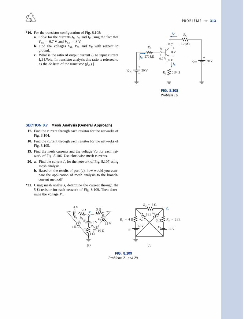
PROBLEMS 313NA
IE
VCC 20 V
RB
270 k
RC
2.2 k
RE 510
IC
8 V
E
C
0.7 V
B
+
–
+ –
–
+
–VCC 20 V
+
IB
*16. For the transistor configuration of Fig. 8.108:a. Solve for the currents IB, IC, and IE using the fact that
VBE 0.7 V and VCE 8 V.b. Find the voltages VB, VC, and VE with respect to
ground.c. What is the ratio of output current IC to input current
IB? [Note: In transistor analysis this ratio is referred toas the dc beta of the transistor (bdc).]
SECTION 8.7 Mesh Analysis (General Approach)
17. Find the current through each resistor for the networks ofFig. 8.104.
18. Find the current through each resistor for the networks ofFig. 8.105.
19. Find the mesh currents and the voltage Vab for each net-work of Fig. 8.106. Use clockwise mesh currents.
20. a. Find the current I3 for the network of Fig. 8.107 usingmesh analysis.
b. Based on the results of part (a), how would you com-pare the application of mesh analysis to the branch-current method?
*21. Using mesh analysis, determine the current through the5- resistor for each network of Fig. 8.109. Then deter-mine the voltage Va.
FIG. 8.108
Problem 16.
FIG. 8.109
Problems 21 and 29.
R1 = 4 3
6
R3 = 5
R5
R2 = 2
E2 16 V12 V
E1
R4
Va
R1
1
5
R5
3
R215 V
E1R4
Va
R3
6 VE2
1
E3
4 V
(a) (b)
10
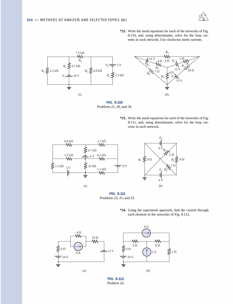
314 METHODS OF ANALYSIS AND SELECTED TOPICS (dc)NA
*23. Write the mesh equations for each of the networks of Fig.8.111, and, using determinants, solve for the loop cur-rents in each network.
R2 3.3 k
E2 3 V
R5 6.8 k
E1 18 V
R1 9.1 k
7.5 k
R4
R3 2.2 k
(I) (II)
R5
4
R4
4
E1
16 V4
R17
R6
E2
12 V
3
R2R3
E3
15 V
10
FIG. 8.110
Problems 22, 30, and 34.
R1
2
1
R3
8
9 V
6 V
E2
R4
(b)
4
6 V
E1
R2
6.8 k 2.7 k
4.7 k
6 V
1.1 k22 k
8.2 k2.2 k
5 V1.2 k
(a)
FIG. 8.111
Problems 23, 31, and 55.
*24. Using the supermesh approach, find the current througheach element of the networks of Fig. 8.112.
FIG. 8.112
Problem 24.
(b)
1
6
20 V
3 A4
8
8 A
(a)
4
24 V
6
10
6 A12 V
*22. Write the mesh equations for each of the networks of Fig.8.110, and, using determinants, solve for the loop cur-rents in each network. Use clockwise mesh currents.
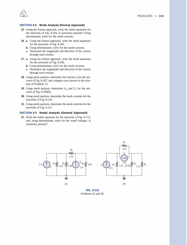
PROBLEMS 315NA
SECTION 8.8 Mesh Analysis (Format Approach)
25. Using the format approach, write the mesh equations forthe networks of Fig. 8.104. Is symmetry present? Usingdeterminants, solve for the mesh currents.
26. a. Using the format approach, write the mesh equationsfor the networks of Fig. 8.105.
b. Using determinants, solve for the mesh currents.c. Determine the magnitude and direction of the current
through each resistor.
27. a. Using the format approach, write the mesh equationsfor the networks of Fig. 8.106.
b. Using determinants, solve for the mesh currents.c. Determine the magnitude and direction of the current
through each resistor.
28. Using mesh analysis, determine the current I3 for the net-work of Fig. 8.107, and compare your answer to the solu-tion of Problem 15.
29. Using mesh analysis, determine I5 and Va for the net-work of Fig. 8.109(b).
30. Using mesh analysis, determine the mesh currents for thenetworks of Fig. 8.110.
31. Using mesh analysis, determine the mesh currents for thenetworks of Fig. 8.111.
SECTION 8.9 Nodal Analysis (General Approach)
32. Write the nodal equations for the networks of Fig. 8.113,and, using determinants, solve for the nodal voltages. Issymmetry present?
FIG. 8.113
Problems 32 and 38.
R2 4
R4
2
3 A
I2R35
R12
5 AI1
(a)
R45
I2
R320 R1 2
4 AI1
(b)
R2
4
2 A
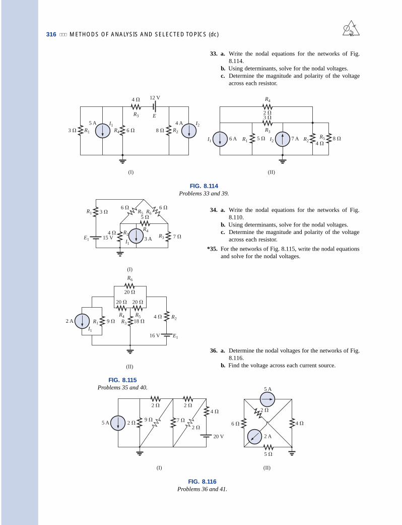
316 METHODS OF ANALYSIS AND SELECTED TOPICS (dc)NA
34. a. Write the nodal equations for the networks of Fig.8.110.
b. Using determinants, solve for the nodal voltages.c. Determine the magnitude and polarity of the voltage
across each resistor.
*35. For the networks of Fig. 8.115, write the nodal equationsand solve for the nodal voltages.
R28
R3
4
4 A I2R4 6 R13
5 A I1
(I)
E
12 V
R24
I26 AI1
(II)
R4
2
R1 5 7 A
R3
3
R5 8
FIG. 8.114
Problems 33 and 39.
I115 V 3 AE1
(I)
R1 3
R24
R56
R3 7 R4
5
6 R6
2 A
I1
(II)
R1 9
R6
20
R4
20
R5
20
R3 18 R24
E116 V
FIG. 8.115
Problems 35 and 40.
36. a. Determine the nodal voltages for the networks of Fig.8.116.
b. Find the voltage across each current source.
(I) (II)
4 6
2 A
5 A
2
5
2 5 A
9
20 V
2
2
4 2
7
FIG. 8.116
Problems 36 and 41.
33. a. Write the nodal equations for the networks of Fig.8.114.
b. Using determinants, solve for the nodal voltages.c. Determine the magnitude and polarity of the voltage
across each resistor.

PROBLEMS 317NA
40 3 A
16 V
4 A
10
6 2 A 12
(I) (II)
4
24 V
20
FIG. 8.117
Problems 37 and 56.
Rs 6 R5
5
R1
5
10
R3
R4
R2
5
20 6 VE
FIG. 8.118
Problems 42 and 43.
Rs 2 k
R5
36 k
R1
33 k
R4
R2
56 k
5.6 k24 VE
R3
3.3 k
FIG. 8.119
Problems 44 and 45.
*37. Using the supernode approach, determine the nodal volt-ages for the networks of Fig. 8.117.
SECTION 8.10 Nodal Analysis (Format Approach)
38. Using the format approach, write the nodal equations forthe networks of Fig. 8.113. Is symmetry present? Usingdeterminants, solve for the nodal voltages.
39. a. Write the nodal equations for the networks of Fig.8.114.
b. Solve for the nodal voltages.c. Find the magnitude and polarity of the voltage across
each resistor.
40. a. Write the nodal equations for the networks of Fig.8.115.
b. Solve for the nodal voltages.c. Find the magnitude and polarity of the voltage across
each resistor.
41. Determine the nodal voltages for the networks of Fig.8.116. Then determine the voltage across each currentsource.
SECTION 8.11 Bridge Networks
42. For the bridge network of Fig. 8.118:a. Write the mesh equations using the format approach.b. Determine the current through R5.c. Is the bridge balanced?d. Is Equation (8.4) satisfied?
43. For the network of Fig. 8.118:a. Write the nodal equations using the format approach.b. Determine the voltage across R5.c. Is the bridge balanced?d. Is Equation (8.4) satisfied?
44. For the bridge of Fig. 8.119:a. Write the mesh equations using the format approach.b. Determine the current through R5.c. Is the bridge balanced?d. Is Equation (8.4) satisfied?
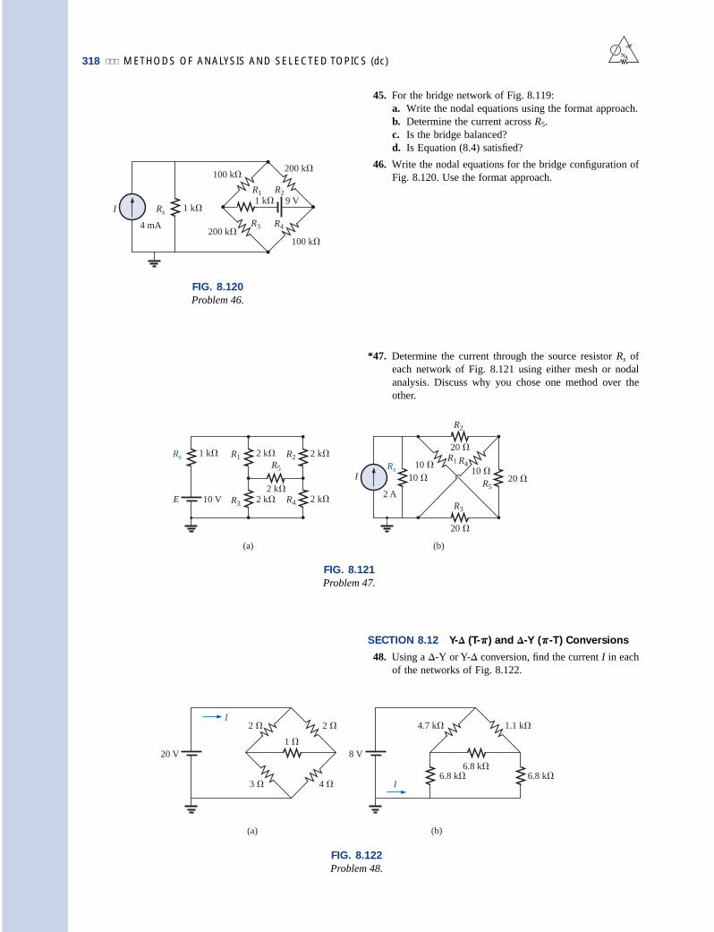
318 METHODS OF ANALYSIS AND SELECTED TOPICS (dc)NA
45. For the bridge network of Fig. 8.119:a. Write the nodal equations using the format approach.b. Determine the current across R5.c. Is the bridge balanced?d. Is Equation (8.4) satisfied?
46. Write the nodal equations for the bridge configuration ofFig. 8.120. Use the format approach.
SECTION 8.12 Y-D (T-p) and D-Y (p-T) Conversions
48. Using a D-Y or Y-D conversion, find the current I in eachof the networks of Fig. 8.122.
*47. Determine the current through the source resistor Rs ofeach network of Fig. 8.121 using either mesh or nodalanalysis. Discuss why you chose one method over theother.
FIG. 8.120
Problem 46.
9 VR1
100 k
R4
100 k
R2
200 k
1 k
R34 mA
Rs 1 kI
200 k
FIG. 8.121
Problem 47.
20 10
R2
R52 A
RsR4
(b)
20 R1
R3
20
10 10 I
R1 2 k
E
(a)
Rs 1 k 2 k R2
10 V R3 2 k 2 kR4
R5
2 k
FIG. 8.122
Problem 48.
20 V
I2
4
1
(a)
2
3
8 V
I
4.7 k
6.8 k
(b)
1.1 k
6.8 k 6.8 k

PROBLEMS 319NA
*50. Determine the current I for the network of Fig. 8.124.
*51. a. Replace the T configuration of Fig. 8.125 (composedof 6-k resistors) with a p configuration.
b. Solve for the source current Is1.
5 A
I
3 k
3 k 6 k
3 k2 k
3 k
3 k
FIG. 8.124
Problem 50.
*52. a. Replace the p configuration of Fig. 8.126 (composedof 3-k resistors) with a T configuration.
b. Solve for the source current Is.
E1 10 V+
–E2 5 V
+
–R3 6 k
R2
6 k
R1
6 kIs1
FIG. 8.125
Problem 51.
E 20 VR5
Rs 1 k
Is
R4 3 k
R3
3 k
R1 2 k R2 2 k
3 k
FIG. 8.126
Problem 52.
*49. Repeat Problem 48 for the networks of Fig. 8.123.
(a) (b)
400 V
I
4 k42 V
I
4 k
6 k
4 k
18
6 6
6 18 18
FIG. 8.123
Problem 49.

320 METHODS OF ANALYSIS AND SELECTED TOPICS (dc)NA
RT
9 9
9
9 9
9 9
9
a b
cd
h g
fe
FIG. 8.127
Problem 53.
*53. Using Y-D or D-Y conversions, determine the total resis-tance of the network of Fig. 8.127.
SECTION 8.14 Computer Analysis
PSpice or Electronics Workbench
54. Using schematics, find the current through each elementof Fig. 8.104.
*55. Using schematics, find the mesh currents for the networkof Fig. 8.111(a).
*56. Using schematics, determine the nodal voltages for thenetwork of Fig. 8.117(II).
Programming Language (C, QBASIC, Pascal, etc.)
57. Given two simultaneous equations, write a program tosolve for the unknown variables.
*58. Using mesh analysis and determinants, write a programto solve for both mesh currents of the network of Fig.8.26 (for any component values).
*59. Using nodal analysis and determinants, write a programto solve for the nodal voltages of the network of Fig. 8.44(for any component values).
GLOSSARY
Branch-current method A technique for determining thebranch currents of a multiloop network.
Bridge network A network configuration typically having adiamond appearance in which no two elements are in seriesor parallel.
Current sources Sources that supply a fixed current to a net-work and have a terminal voltage dependent on the networkto which they are applied.
Delta (D), pi (p) configuration A network structure thatconsists of three branches and has the appearance of theGreek letter delta (D) or pi (p).
Determinants method A mathematical technique for findingthe unknown variables of two or more simultaneous linearequations.
Mesh analysis A technique for determining the mesh (loop)currents of a network that results in a reduced set of equa-tions compared to the branch-current method.
Mesh (loop) current A labeled current assigned to each dis-tinct closed loop of a network that can, individually or incombination with other mesh currents, define all of thebranch currents of a network.
Nodal analysis A technique for determining the nodal volt-ages of a network.
Node A junction of two or more branches in a network.Wye (Y), tee (T) configuration A network structure that
consists of three branches and has the appearance of thecapital letter Y or T.