mfpa: mixed-signal field programmable array for …
TRANSCRIPT

MFPA: MIXED-SIGNAL FIELD PROGRAMMABLE ARRAY FOR ENERGY-AWARE COMPRESSIVE SIGNAL PROCESSING
by
ADRIAN TATULIAN
B.S. University of Central Florida, 2013
A thesis submitted in partial fulfillment of the requirements
for the degree of Master of Science in the Department of Electrical and Computer Engineering
in the College of Engineering and Computer Science at the University of Central Florida
Orlando, Florida
Spring Term 2020
Major Professor: Ronald F. DeMara

ii
© 2020 Adrian Tatulian

iii
ABSTRACT
Compressive Sensing (CS) is a signal processing technique which reduces the number of
samples taken per frame to decrease energy, storage, and data transmission overheads, as well as
reducing time taken for data acquisition in time-critical applications. The tradeoff in such an
approach is increased complexity of signal reconstruction. While several algorithms have been
developed for CS signal reconstruction, hardware implementation of these algorithms is still an
area of active research. Prior work has sought to utilize parallelism available in reconstruction
algorithms to minimize hardware overheads; however, such approaches are limited by the
underlying limitations in CMOS technology. Herein, the MFPA (Mixed-signal Field
Programmable Array) approach is presented as a hybrid spin-CMOS reconfigurable fabric
specifically designed for implementation of CS data sampling and signal reconstruction. The
resulting fabric consists of 1) slice-organized analog blocks providing amplifiers, transistors,
capacitors, and Magnetic Tunnel Junctions (MTJs) which are configurable to achieving
square/square root operations required for calculating vector norms, 2) digital functional blocks
which feature 6-input clockless lookup tables for computation of matrix inverse, and 3) an MRAM-
based nonvolatile crossbar array for carrying out low-energy matrix-vector multiplication
operations. The various functional blocks are connected via a global interconnect and spin-based
analog-to-digital converters. Simulation results demonstrate significant energy and area benefits
compared to equivalent CMOS digital implementations for each of the functional blocks used: this
includes an 80% reduction in energy and 97% reduction in transistor count for the nonvolatile
crossbar array, 80% standby power reduction and 25% reduced area footprint for the clockless

iv
lookup tables, and roughly 97% reduction in transistor count for a multiplier built using
components from the analog blocks. Moreover, the proposed fabric yields 77% energy reduction
compared to CMOS when used to implement CS reconstruction, in addition to latency
improvements.

v
ACKNOWLEDGMENTS
First and foremost, I would like to thank my advisor, Dr. DeMara, for welcoming me into
the Computer Architecture Laboratory and since then always being there to support me whether
that meant proofreading a paper, recommending courses, or simply encouraging me that I’m on
the right track. As a result, I was able to complete this thesis and serve as co-author on two IEEE
publications within two years of coming into the program as an out-of-field student with very
limited ECE knowledge. In addition, I would like to thank Dr. Nazanin Rahnavard and Dr. Damian
Dechev for agreeing to serve on my thesis committee.
Finally, this work was supported in part by the Center for Probabilistic Spin Logic for Low-
Energy Boolean and Non-Boolean Computing (CAPSL), one of the Nanoelectronic Computing
Research (nCORE) Centers as task 2759.006, a Semiconductor Research Corporation (SRC)
program sponsored by the NSF through CCF-1739635, and by NSF through ECCS-1810256.
vi
TABLE OF CONTENTS
LIST OF FIGURES …………………………………………………………………………….viii
LIST OF TABLES …………………………………………………………………………….….x
CHAPTER ONE: INTRODUCTION ............................................................................................. 1
Need for Mixed-Signal Reconfigurable Arrays .......................................................................... 1
Compressive Sensing .................................................................................................................. 2
Spin-Based Computation and Architectural Approaches ........................................................... 5
Contributions and Organziation of Thesis ................................................................................. 9
CHAPTER TWO: RELATED WORK ......................................................................................... 12
Mixed-Signal Arrays ................................................................................................................. 12
NVM-Based FPGAs ................................................................................................................. 14
Hardware for Implementation of CS Sampling ........................................................................ 17
Hardware for Implementation of CS Reconstruction ............................................................... 21
Summary ................................................................................................................................... 25
CHAPTER THREE: MFPA PLATFORM ................................................................................... 27
NVM Crossbar .......................................................................................................................... 29
Configurable Digital Blocks (CDBs) ....................................................................................... 31
Configurable Analog Blocks (CABs) ....................................................................................... 33

vii
CHAPTER FOUR: ENERGY AND DELAY PERFORMANCE................................................ 35
NVM Crossbar .......................................................................................................................... 35
CDB .......................................................................................................................................... 36
CAB .......................................................................................................................................... 37
CHAPTER FIVE: ASSESSMENT OF ERROR TOLERANCE.................................................. 41
OMP .......................................................................................................................................... 42
CoSaMP .................................................................................................................................... 44
AMP .......................................................................................................................................... 45
CHAPTER SIX: FABRIC-BASED CS REALIZATION ............................................................ 49
Sampling Architecture .............................................................................................................. 49
Reconstruction Architecture ..................................................................................................... 50
Further Benefits ........................................................................................................................ 55
CHAPTER SEVEN: CONCLUSIONS ........................................................................................ 56
Technical Summary and Insights .............................................................................................. 56
Scope and Limitations .............................................................................................................. 59
Future Work .............................................................................................................................. 59
APPENDIX: COPYRIGHT PERMISSIONS ............................................................................... 61
REFERENCES ............................................................................................................................. 63
viii
LIST OF FIGURES
Fig. 1: Outline of thesis. Preliminary versions of some of this work appeared as a first author
publication in the 2019 International Conference on Reconfigurable Computing and FPGAs
[35]. .......................................................................................................................................... 11
Fig. 2: Summary of selected previous approaches to beyond-CMOS NVM integration in
reconfigurable fabrics .............................................................................................................. 17
Fig. 3: Summary of challenges and solutions relating to hardware implementation of
Compressive Sensing. Each of the listed challenges is addressed by MFPA, as discussed in
Chapter 1. .................................................................................................................................. 21
Fig. 4: (a) Single-slice organization for proposed MFPA architecture, b) MFPA routing and
switch interconnect design, and (c) Hybrid spin/charge device realization as configurable
blocks within the MFPA fabric ................................................................................................. 28
Fig. 5: MFPA NVM Crossbar consisting of 1 MTJ per cell for In-Memory Computing, where
red signals show the configuration flow, the blue signals depict the path for populating the
measurement matrix and green signals illustrate the path for VMM operation ....................... 30
Fig. 6: (a) MFPA CDB structure and (b) C-LUT circuit components utilized for CDB logic
select/retrieval [3] ..................................................................................................................... 32
Fig. 7: (a) MFPA CAB structure and (b) configuration of an analog multiplier circuit using
CAB elements .......................................................................................................................... 34

ix
Fig. 8: Reconstruction error using OMP .................................................................................. 43
Fig. 9: Reconstruction error using CoSaMP ............................................................................ 45
Fig. 10: Reconstruction error using AMP ................................................................................ 47
Fig. 11: Hardware architecture for AMP reconstruction ......................................................... 52
Fig. 12: Logical organization of this thesis .............................................................................. 57

x
LIST OF TABLES
Table 1: Comparison of mixed-signal field-programmable fabrics which are suitable for
various signal processing tasks. ................................................................................................ 14
Table 2: Comparison of energy needed for VMM in CMOS crossbar vs. proposed NVM
crossbar. ................................................................................................................................... 36
Table 3: Data for analog squaring circuit. ............................................................................... 38
Table 4: Data for analog square root circuit. .......................................................................... 39
Table 5: Data for analog inverse square root circuit. ............................................................... 39
Table 6: Minimum number of measurements needed for -60 dB error, using exact and
approximate square-square root operations. ............................................................................ 48
Table 7: MFPA energy costs. .................................................................................................. 53
Table 8: Energy for AMP. ....................................................................................................... 54

1
CHAPTER ONE: INTRODUCTION1
Need for Mixed-Signal Reconfigurable Arrays
The flexibility offered by reconfigurable fabrics has proven to be useful in signal
processing applications. For instance, Huang et al. described an FPGA-based scalable architecture
for computation of Discrete Cosine Transform (DCT) in image-video coding applications [1].
FPGAs allow for dynamic partial reconfiguration for zonal coding, i.e., performing DCT on zones
varying in size from 1×1 to 8×8, as well as reconfigurability in the precision of DCT coefficients.
It was shown that having this flexibility allows for optimizations which result in significant savings
in both power and area consumption.
While digital-only FPGAs can be convenient for online algorithms requiring dynamic
reconfiguration [2] and conducting general-purpose computation directly in hardware to avoid
software overheads [3, 4], computations in the signal processing domain can generally be more
efficiently solved in the analog domain due to the analog nature of real-world signals [5]. Thus,
Field Programmable Analog Arrays (FPAAs) have gained attention as analog counterparts to
FPGAs. It has been shown that analog computation for certain applications can offer orders of
magnitude improvement in computational energy efficiency at the cost of reduced accuracy [6].
Therefore, judicious use of analog and mixed-signal computation may lead to benefits in various
applications suitable for approximate computation. Mixed-signal arrays have already been used
1© 2020 IEEE. Part of this chapter is reprinted, with permission, from [35].

2
for applications such as low-power temperature sensors and heart-rate alarms for IoT applications
[7].
Unfortunately, analog systems present many challenges not present in their digital
counterparts such as limited accuracy, low tolerance to noise and parasitics, and limited
programmability. As such, analog design automation has been a field of active research, and
algorithms have been developed for analog synthesis, layout and verification. It has been found
that using a set of Configurable Analog Blocks (CABs), each with fixed layout, allows for a
bounded synthesis problem and leads to an Electronic Design Automation (EDA) flow similar to
that used in digital design [8].
Compressive Sensing
Compressive Sensing (CS) is an emerging signal processing technique that is well-suited
for analog computation. The objective in CS is to reconstruct a sparse signal, i.e., a signal with
only a small number of non-zero values in some basis, using sub-Nyquist sampling rates. This
achieves reduced energy, storage, and data transmission overheads [9, 10], in addition to reducing
sampling duration in time-sensitive applications such as MRI [11]. CS consists of a sampling
phase, followed by a reconstruction phase.
During the sampling phase, measurements on the signal of interest are taken at a specified
rate and quantization resolution. The objective of the sampling phase is to determine a compressed
measurement vector, 𝒚𝒚𝜖𝜖ℝ𝑀𝑀, based on the signal vector, 𝒙𝒙𝜖𝜖ℝ𝑁𝑁, where 𝑀𝑀 ≪ 𝑁𝑁. A measurement
matrix 𝜱𝜱𝜖𝜖ℝ𝑀𝑀×𝑁𝑁 is used to achieve this using the transformation 𝒚𝒚 = 𝜱𝜱𝒙𝒙. Different methods exist

3
for generating the CS measurement matrix: one is by populating the entire matrix using values
from a Gaussian distribution. Another is by restricting matrix elements to either ‘1’ or ‘0’, and
simply populating each column of the matrix with a set number of ‘1’s placed at random locations.
The randomness of the measurement matrix ensures that the signal is uniformly sampled, i.e., no
one part of the signal is given special consideration. In certain situations, signals may contain a
specific region of interest: in this case, it is desirable to sample the region of interest at a higher
rate, and thus a higher column weight (i.e., higher density of ‘1’s) is used for columns
corresponding to the signal’s region of interest [12].
The reconstruction phase of Compressive Sensing entails solving 𝒚𝒚 = 𝜱𝜱𝒙𝒙 to reconstruct
the signal vector, 𝒙𝒙. Since the matrix 𝜱𝜱 contains more columns than rows, this amounts to solving
an undetermined system of linear equations with more unknowns than equations, and hence an
infinite number of solutions. In CS, the solution with lowest sparsity rate, i.e., lowest density of
nonzero elements, is selected. This amounts to solving the minimization problem: 𝐱𝐱� =
argmin‖𝒙𝒙‖0 s.t. 𝒚𝒚 = 𝜱𝜱𝒙𝒙. Unfortunately, this problem has been shown to be NP-hard and is
therefore not practical to solve [9]. Thus, it is more common to approach signal reconstruction
using the basis pursuit problem [10]: 𝐱𝐱� = argmin‖𝒙𝒙‖1 s.t. 𝒚𝒚 = 𝜱𝜱𝒙𝒙 , otherwise known as ℓ1 -
minimization. By shifting focus from the ℓ0 norm to the ℓ1 norm, the problem becomes convex
and therefore computationally more tractable to solve. The condition for being able to do this is
known as the Restricted Isometry Property (RIP), i.e., that for any k-sparse vector x,
‖𝒙𝒙‖𝑝𝑝(1− 𝛿𝛿) ≤ ‖𝜱𝜱𝒙𝒙‖𝑝𝑝 ≤ ‖𝒙𝒙‖𝑝𝑝(1 + 𝛿𝛿) for some specified p.

4
In addition to basis pursuit, a wide variety of algorithms with different tradeoffs are
available for CS reconstruction [13]. One such algorithm which has been heavily targeted by
hardware designers is Orthogonal Matching Pursuit (OMP). OMP is a greedy algorithm which
seeks to use a set of k column vectors from the 𝜱𝜱 matrix as a basis to represent y. The challenge is
to select the right column vectors, and then use this information to reconstruct the original signal
vector, x. The algorithm works by repeatedly picking columns of 𝜱𝜱 with maximum correlation to
the remaining part of y. At each iteration, the algorithm solves a least-squares problem to pick an
optimal solution for x, based on the columns of 𝜱𝜱 which have been picked so far. Based on 𝜱𝜱 and
x, the algorithm then calculates y and subtracts this from actual y to determine the new residual
vector before going to the next iteration. For a k-sparse signal, the objective is to attain an exact
representation of the original signal after k iterations [14, 15]. In reality, the reconstruction will not
be exact due to unavoidable measurement noise in the sampling process. The precise steps of OMP
are outlined in Algorithm 1.

5
Spin-Based Computation and Architectural Approaches
A common issue with FPGAs is errors caused by faults such as process variation and cosmic
ray interference. Hence, fault tolerance in FPGAs has been a widely-researched area [16-19] and
has included methods such as evolutionary computation [20, 21], asynchronous logic [22, 23], and
modular redundancies [24, 25]. Each of these solutions presents significant overheads in terms of
power and area. This, in addition to challenges relating to CMOS scaling and power consumption,
has motivated researchers to explore emerging devices as an alternative or complement to CMOS-
based logic. Indeed, emerging devices such as quantum cellular automata (QCA) [26], domain

6
wall nanomagnets [27], and spin-based devices [28, 29] have demonstrated superior performance
in designs such as full adder and sense amplifier circuits. While several beyond-CMOS alternatives
currently exist, the focus in this work will be on spin-based devices due to their commercial
availability and benefits listed below.
Spin-based devices, specifically Spin Transfer Torque-based Magnetic Tunnel Junctions
(STT-MTJs), are a form of post-CMOS technology which serve as the basis for Magnetic Random
Access Memory (MRAM) in addition to having logic capabilities. MTJ’s offer numerous benefits
such as nonvolatility, near-zero static power consumption, area efficiency, fast read operation, and
ability to be vertically integrated with CMOS for area efficiency [30]. STT-MTJs consist of two
ferromagnetic layers, referred to as the fixed and free layers and separated by a thin oxide barrier.
A bi-directional current passing through the device can change the polarization of the free layer
magnetization and thus flip the device between the parallel (P) state and the anti-parallel (AP)
state. The P-state device resistance is given by 𝑅𝑅𝑃𝑃 = 𝑅𝑅𝑀𝑀𝑀𝑀𝑀𝑀 while the AP-state resistance is given
by 𝑅𝑅𝐴𝐴𝑃𝑃 = 𝑅𝑅𝑀𝑀𝑀𝑀𝑀𝑀(1 + 𝑇𝑇𝑀𝑀𝑅𝑅), where:
𝑅𝑅𝑀𝑀𝑀𝑀𝑀𝑀 = 𝑡𝑡𝑜𝑜𝑜𝑜𝐹𝐹𝐹𝐹𝐹𝐹𝑡𝑡𝐹𝐹𝐹𝐹×𝐴𝐴𝐹𝐹𝐴𝐴𝐹𝐹�𝜑𝜑
𝑒𝑒𝑒𝑒𝑒𝑒(1.025𝑡𝑡𝐹𝐹𝑜𝑜�𝜑𝜑) (1)
𝑇𝑇𝑀𝑀𝑅𝑅 = 𝑀𝑀𝑀𝑀𝑇𝑇0
1+�𝑉𝑉𝑏𝑏𝑉𝑉ℎ�2 (2)
with TMR being tunneling magnetoresistance, tox the oxide layer thickness, Factor a material-
dependent parameter which depends on the resistance-area product of the device, Area the surface
area of the device, 𝜑𝜑 the oxide layer energy barrier height, Vb bias voltage, and Vh the bias voltage
at which TMR drops to half of its initial value.

7
In order for an MTJ to switch states, an energy barrier must be overcome. This switching
process can occur in several ways; however, the two most practical methods are Spin Transfer
Torque (STT) and Spin Hall Effect (SHE) switching. In STT switching, a spin-polarized current
passing through the device transfers angular momentum to electrons in the device’s free layer,
which causes the magnetic moments of these electrons, and hence the free layer magnetization
direction, to switch. In SHE switching, a charge current passing through a heavy metal base layer
can induce spin-polarized current to pass through the device, causing switching as before. While
STT devices are two-terminal with only one read/write path, SHE devices are three-terminal with
separate read and write paths. Hence, the probability for write disturbance in these devices is lower,
in addition to lower write latencies [10].
MTJs are also capable of switching stochastically due to thermal noise, if the energy barrier
is set to a sufficiently low value (≪ 40 kT, where k is Boltzmann’s constant and T is absolute
temperature). The stochastic switching property has valuable applications when random or non-
deterministic outputs are necessary [10]. While spin-based devices have been researched in
academia for several years, they are now also gaining commercial ground, with Intel announcing
the availability of 1T1MTJ MRAM cells in conjunction with their 22-nm FinFET technology [31].
MTJs contribute valuable properties such as non-volatility and stochasticity, allowing them to
be suitable for diverse applications. One application is the fracturable 6-input spin-based look-up
table, proposed in [32] and upgraded to utilize the Spin Hall Effect [33] and operate
asynchronously as a Clockless-LUT (C-LUT) design [3]. The C-LUT’s select tree consists of D
levels of transmission gates, each controlling access to a spin-based memory cell. The memory

8
cells consist of pairs of complementary MTJs for a wide read margin yielding reliable read
operation. Furthermore, sensing is accomplished through a voltage divider circuit and a pair of
inverters to amplify the signal, which eliminates the need for an external clock or large sense
amplifiers. Such a design can be used for combinational logic to implement either one D-input
Boolean function, or two (D-1)-input Boolean functions in parallel. This design yields an 80%
reduction on standby power consumption compared to an SRAM-based LUT, which addresses a
key challenge faced by CMOS designs.
In addition, the stochastic switching properties of low-energy-barrier MTJs can be used to
implement a True Random Number Generator (TRNG) to generate an adaptive CS measurement
matrix [10, 34]. This design is based on a p-bit, which divides the supply voltage VDD between an
MTJ and NMOS transistor. The MTJ is fabricated to have a low energy barrier (~1 kT) between P
and AP states, and hence switches due to thermal activation. The p-bit utilizes the voltage in
between the two devices, which switches stochastically due to the stochastic switching of the MTJ
device. The p-bit output serves as the input to a D flip-flop, which then generates a random M-bit
stream, where each bit determines one row of the measurement matrix, for random sampling of
the input signal. The TRNG used in this design was found to reduce energy consumption per bit
by 9-fold on average, compared to state-of-the-art TRNGs, in addition to an average area reduction
of 3-fold [10].
To support mixed-signal operation and conversion, an Adaptive Intermittent Quantizer (AIQ)
is a suitable spintronic circuit. It utilizes the Voltage-Controlled Magnetic Anisotropy (VCMA)
effect to dynamically control MTJ energy barriers to implement an Analog-to-Digital Converter

9
(ADC) featuring dynamic Sampling Rate/Quantization Resolution (SR/QR) tradeoff [30]. In this
design, the MTJs are arranged in a resistive-switch-ladder architecture, with the analog signal as
input. Dynamically controlling the states of the switches and control over the number of active
devices in the circuit allows the architecture to function at various QRs; in addition, use of an
asynchronous clock allows the SR to be dynamically set as well. The SR/QR tradeoff is determined
by the Signal-to-Noise (SNR) ratio of the input signal, e.g., high SNR favors high QR when
sampling. As expected, this technique allows ADC at fixed bit and energy budgets, and results in
considerable energy savings overall. Thus, spin-based architectures offer key benefits in power
and area consumption when compared to CMOS and are promising candidates for next-generation
reconfigurable fabrics.
Contributions and Organization of Thesis
In this work, a hybrid spin-CMOS Mixed-signal Field Programmable Array (MFPA) is
proposed for Compressive Sensing applications. The proposed MFPA architecture consists of
Configurable Analog Blocks (CABs), Configurable Digital Blocks (CDBs) and an MRAM-based
Nonvolatile Crossbar Array (NVM Xbar) joined by a CMOS-based global interconnect. While CS
can provide benefits such as reduced data storage and transmission costs, applications such as
Internet of Things (IoT) devices also require minimal power consumption. Mixed-signal
computing and spin-based devices are viable approaches for achieving this due to many advantages
offered by this approach, including:

10
a) intrinsic computation for reduced hardware complexity: time- and power-consuming
operations such as square root are performed in one cycle using a simple circuit, with no digital-
to-analog conversion needed due to input signals already being analog,
b) stochasticity for true random number generation: spin-based devices offer a low-energy
method of achieving random number generation necessary for CS algorithms,
c) power and area efficiency: spin-based devices do not have leakage power constraints like
CMOS and furthermore can be integrated vertically with CMOS for reduced area overhead, and
d) efficient VMM: spin-based devices can be readily integrated into crossbar arrays for single-
cycle Vector-Matrix Multiplication (VMM) operations. Thus, the hypothesis is that the proposed
design will be capable of performing CS sampling and reconstruction while delivering significant
energy and area benefits compared to the conventional digital CMOS implementation.
The thesis is organized as illustrated by Fig. 1: Chapter 2 reviews related works in the
fields of reconfigurable arrays and hardware-based CS sampling and reconstruction. Chapter 3
outlines the specifics of the hardware proposed herein, beginning with an overview of the
architecture and proceeding to discuss details of the NVM Xbar, CAB and CDB. Each component
is then simulated and compared with an equivalent digital CMOS design in Chapter 4. Chapter 5
proceeds to assess the impact of computation errors associated with CAB analog outputs on CS
reconstruction algorithms. Next, Chapter 6 presents an architecture for implementation of CS
reconstruction using the proposed fabric, and evaluates the design compared to the digital CMOS
equivalent. Finally, Chapter 7 concludes the thesis by giving a technical summary, and outlining
insights gained and future work in the field.

11
Chapter 1: Introduction Chapter 2: Related Works Chapter 3: The MFPA Platform Chapter 4: Energy and Delay Performance Chapter 5: Assessment of Error Tolerance
Chapter 6: Fabric-Based CS Realization
Chapter 7: Conclusions
Fig. 1: Outline of thesis. Preliminary versions of some of this work appeared as a first author publication in the 2019 International Conference on Reconfigurable Computing and FPGAs [35].
OMP CoSaMP AMP
NVM Crossbar Configurable Digital Blocks
Configurable Analog Blocks
Need for mixed-signal arrays
Compressive Sensing
Contributions/ organization
Spin-based architectures
Mixed-signal arrays
Hardware for CS sampling
Hardware for CS reconstruction
NVM-based FPGAs
Summary
NVM Crossbar CDBs CABs
Reconstruction architecture
Further benefits
Sampling architecture
Technical summary
Future work Scope and limitation

12
CHAPTER TWO: RELATED WORKS2
Mixed-signal Arrays
Schlottmann and Hasler [36] noted that two main hurdles have hindered the widespread
adaptation of analog computation: the lack of a programmable interface, and the lack of robust
design tools. The Reconfigurable Analog Signal Processor (RASP) proposed by them was a
groundbreaking development in FPAAs in that it provided an avenue for programmability of
analog devices, and was further augmented through an integrated set of high-level tools for system-
level analog design. Since this breakthrough, there has been continued innovation in development
of mixed-signal reconfigurable arrays, i.e., those containing both analog and digital computation.
Wunderlich [5] presented a Field Programmable Mixed Array (FPMA) interleaving both
analog and digital elements in a Manhattan-routable fabric. Their design consisted of
Computational Analog Blocks (CABs) as well as Computational Logic Blocks (CLBs) interwoven
through a global interconnect. The CLBs were comprised of LUTs and D Flip-Flops (D-FFs) while
the CABs were comprised of elements such as capacitors, transistors, and op-amps. Additionally,
each block contained a local interconnect consisting of a set of reconfigurable switches.
George [37] proposed a similar architecture which also integrated a 16-bit microprocessor for
added computational capability, thus enabling a 1,000-fold improvement in energy efficiency in
addition to a 100-fold decrease in die area compared to the digital equivalent. Finally, Choi [38]
proposed an architecture which consisted of three separate arrays of CLBs, Arithmetic Logic Units
2 © 2020 IEEE. Part of this chapter is reprinted, with permission, from [35].

13
(ALUs) and Time-domain Configurable Analog Blocks (TCABs), with a network of “gluing
blocks” interfacing the arrays with one another as well as external input/output. TCABs allow for
dynamic reconfigurability of the analog function being implemented, in contrast to CABs which
only allow for reconfigurability of interconnects.
Pyle [39] further built on earlier efforts implementing evolutionary computation on FPGAs [4,
40, 41] to explore the possibility of analog computation of mathematical functions, specifically,
the square, square root, cube, and cube root functions. Pyle’s approach was to use a Self-Scaling
Genetic Algorithm (SSGA) to scale the function parameters to an acceptable range, at which point
the computations were performed on an analog fabric and refined through a process of Differential
Digital Correction (DDC), using the Cypress PSoC-5LP chip [39]. This approach was later
extended to more generalized mathematical functions by Thangavel [42] by extending these
functions for Puiseux series generalization accommodating negative and fractional exponents as
power series algebraic expansions.

14
Table 1 summarizes the various approaches provided by the above-mentioned authors and
provides a comparison to the design proposed herein.
NVM-Based FPGAs
Nonvolatile memories (NVMs), including memristors, Phase Change Memory (PCM), and
Spin Torque Transfer-based Magnetic Random Access Memory (STT-MRAM) offer several
advantages to conventional SRAM, including low static power consumption, high area density,
and non-volatility. Thus, integration of these devices into FPGAs has been a popular research
interest in recent years. Many works have focused on one of two options: replacing SRAM with
NVMs as the storage element in look-up tables (LUTs), or replacing SRAM with NVM in routing
Table 1: Comparison of mixed-signal field-programmable fabrics which are suitable for various signal processing tasks.
Work Routing Architecture CAB Elements CDB Elements Highlighted Contributions
Wunderlich [5] Manhattan Operational transconductance
amplifiers, transistors, capacitors, MITEs (multiple input translinear
elements)
3-input Basic logic element (BLE)
Integrated analog/digital computation
George [36] Manhattan w/ μProc. Cores
Operational transconductance amplifiers, transistors, multipliers
4-input Basic logic element (BLE)
Integrated microprocessor with CABs/CLBs
Choi [37] Separate TCAB/ ALU/CLB arrays
Time configurable analog blocks (TCABs)
4-input programmable LUT Programmability using TCABs
Schlottmann [35] Crossbar Operational transconductance amplifiers, transistors N/A Dynamically reconfigurable
FPAA M-FPA
(proposed herein) Crossbar Amplifiers, transistors, capacitors, low-/high-barrier MTJs
6-input Fracturable C-LUT
Spin-based FPA with NVM crossbar for CS applications

15
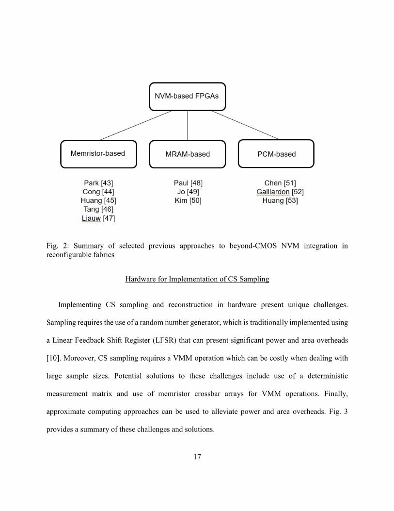
elements such as switching blocks (SBs) and connection blocks (CBs) [43, 44]. Fig. 2 gives a
summary of selected works relating to NVM integration in FPGAs.
Cong [44] proposed using memristive crossbar arrays to implement switching blocks in the
FPGA fabric. In this scheme, memristors and metal wires are stacked on top of CMOS access
transistors to reduce area overhead. The authors determined that this optimization reduced the SB
area overhead to negligible amounts, as opposed to CMOS-based SBs which consume 10% - 50%
of the FPGA area. Specifically, a 96% reduction in area, 55% improvement in performance, and
79% reduction in power was attained. Similar results were reported by Huang [45] and Tang [46],
among other authors.
Moreover, Liauw [47] was first to propose using memristors to replace SRAM in LUTs. Park
[43] extended this idea to bring memristors and SRAM together to build hybrid FPGAs consisting
of alternating SRAM-based and NVM-based LUTs. Such hardware allows for both power and
performance optimization by placing SRAM-based logic blocks (superior in speed) on the critical
path of an application, while using NVM-based logic blocks (superior in power consumption)
elsewhere. Indeed, the placement algorithm developed by the authors around this idea attained a
22% average reduction in power consumption on the benchmarks tested, with only negligible
increase in critical path delay.
In addition to memristors, STT-MRAM can be used as an NVM alternative which offers
advantages in speed, endurance, and density. Paul [48] proposed CLBs with MTJs replacing
SRAM cells, which could then be further improved using Shannon decomposition-based power
gating. He found a 48% reduction in area, 22% delay improvement, and 16% power reduction

16
compared to an equivalent CMOS design. Jo [49] proposed an 8-input MRAM-based LUT which
attained 74% read power improvement compared to CMOS. Finally, Kim [50] designed a CAD
tool for MRAM-based nonvolatile LUTs to address programmability issues that come with
emerging technologies.
PCM is a further NVM possibility, offering high performance, scalability, and high density.
PCM also allows for 3D die stacking, which can further enhance density, as well as performance,
by shortening wire lengths, and power, by reducing parasitic capacitance of wires. In addition,
PCM allows for implementation of Multi-Level Cells (MLCs) which can hold multiple bits within
one device by programming multiple levels of resistances. Chen [51] found significant benefits in
area, leakage power, and read energy by using MLC-PCM to replace SRAM in LUTs and routing
blocks in an FPGA employing a 3D die-stacked architecture. Gaillardon [52] achieved similar
results using PCM-based LUTs. Huang [53] further researched improving PCM retention time and
leakage power, which are two major weaknesses of the technology. By using 0-V biasing during
normal FPGA operation, he was able to reduce active leakage power to 1.19 nW and extend
retention time to 10 years.
17
Fig. 2: Summary of selected previous approaches to beyond-CMOS NVM integration in reconfigurable fabrics
Hardware for Implementation of CS Sampling
Implementing CS sampling and reconstruction in hardware present unique challenges.
Sampling requires the use of a random number generator, which is traditionally implemented using
a Linear Feedback Shift Register (LFSR) that can present significant power and area overheads
[10]. Moreover, CS sampling requires a VMM operation which can be costly when dealing with
large sample sizes. Potential solutions to these challenges include use of a deterministic
measurement matrix and use of memristor crossbar arrays for VMM operations. Finally,
approximate computing approaches can be used to alleviate power and area overheads. Fig. 3
provides a summary of these challenges and solutions.

18
Fardad [54] published a paper outlining the use of deterministic measurement matrices in CS.
His method was based on a parity check matrix based on hyperplanes in Euclidean geometry.
Specifically, for prime p and two integers m > 1 and s > 0, an m-dimensional Euclidean geometry
over the Galois field GF(ps) can be defined. A 𝜇𝜇-dimensional subspace of the vector space of all
m-tuples in this geometry is called a 𝜇𝜇-flat. Choosing two different values of 𝜇𝜇, i.e., 𝜇𝜇1 and 𝜇𝜇2, a
matrix H can be defined with elements hij = 1 if and only if the ith 𝜇𝜇2-flat contains the jth 𝜇𝜇1-flat
(where 𝜇𝜇2 > 𝜇𝜇1). This determines a deterministic, sparse, binary matrix. In CS reconstruction
applications, the authors compared this to a Gaussian matrix and observed similar performance in
terms of percentage of perfect signal reconstructions. In addition to avoiding overheads associated
with random number generation, the authors noted a two-order-of-magnitude reduction in power
consumption when using this matrix for signal reconstruction using OMP, versus the conventional
technique of using a Gaussian matrix.
Leitner [55] proposed a different method of accomplishing CS sampling via a deterministic,
sparse, binary measurement matrix, in the context of image sensors. Their method involves
splitting the image pixels into sets of 𝑁𝑁𝑀𝑀
+ 𝑂𝑂𝑂𝑂 neighboring pixels, where N is the image size, M the
number of measurements taken, and OL the size of the overlap between adjacent pixel sets. In this
context, each measurement is determined by summing the values of all of the neighboring pixels
in its corresponding group. The elements of the measurement matrix are hence given by:
𝜙𝜙𝑖𝑖𝑖𝑖 = �1 𝑖𝑖𝑖𝑖 1 + (𝑖𝑖 − 1)𝑁𝑁𝑀𝑀
≤ 𝑗𝑗 ≤ 𝑖𝑖𝑁𝑁𝑀𝑀
+ 𝑂𝑂𝑂𝑂 0 𝑜𝑜𝑡𝑡ℎ𝑒𝑒𝑒𝑒𝑒𝑒𝑖𝑖𝑒𝑒𝑒𝑒
(3)

19
It is observed that while this matrix does not satisfy the RIP property, it does provide
incoherence with the Inverse Discrete Cosine Transform (IDCT) basis. As such, this matrix works
well with low-frequency images, but fails with high-frequency images. Specifically, the authors
compared the peak signal-to-noise ratio (PSNR) of natural images reconstructed using the
proposed matrix and a Gaussian matrix, using the technique of ℓ1 -minimization. The results
indicated that the proposed matrix outperformed the Gaussian matrix by 3.7 dB, on average. Signal
reconstruction using the proposed matrix failed when using an artificial image comprised of
alternating black and white pixels, though such an image would rarely appear in practice. The
authors noted significant energy savings for an image sensor using this approach, when compared
to previous works relying on LFSRs.
Finally, Jafari [56] proposed constructing a deterministic measurement matrix simply by
choosing rows from the identity matrix, in the context of a wearable chip for seizure detection.
Their results indicated a two-order-of-magnitude reduction in both latency and dynamic power
consumption, compared to an equivalent system using LFSR to generate random matrices.
In contrast to the above techniques employing deterministic measurement matrices,
Massoud [57] proposed using memristors to store the measurement matrix, taking advantage of
their nonvolatility as memory devices, and hybrid logic-memory capabilities. In this approach, the
authors proposed using LFSRs to program each memristor to one of two values, which would then
act as multiplexers to modulate the input signal. Hence, the memristors were effectively being used
to store a binary measurement matrix. The authors observed sufficient reconstruction accuracy

20
using this approach, and cited potential benefits involving chip area, resilience to jitter, and
hardware complexity.
Qian [58] built upon this work by introducing memristor crossbar arrays for VMM operations
during CS sampling. In contrast to Massoud’s approach of using LFSRs to generate random values,
Qian proposed relying on the process variation inherent in memristor filament lengths to generate
randomness. Due to the physical model of a memristor, consisting of a filament growing under
certain connections to establish an electrical connection between two electrodes, randomness in
filament length can result in randomness in device state under identical conditions. The authors
observed that signal reconstruction using ℓ1-minimization yields similar PSNRs to that of using a
Gaussian matrix, while eliminating expensive hardware such as LFSRs and multiply-accumulate
units for digital VMM.
Finally, Kadiyala [59] proposed using approximate computation to reduce power and area
overheads during the sampling stage. Their work was built upon two methods: probabilistic
pruning and probabilistic logic minimization. Probabilistic pruning refers to removing elements of
a circuit which do not make a large difference in the accuracy of the output data, whereas
probabilistic logic minimization refers to flipping bits of certain output states to minimize the logic
overhead. The authors found that when these techniques are applied to the multiply-accumulate
units involved in the VMM architecture of CS sampling, a 54% reduction in power and 43%
reduction in area can be attained at the cost of 1 dB reduction in PSNR.

21
Fig. 3: Summary of challenges and potential solutions relating to hardware implementation of Compressive Sensing. Each of the listed challenges is addressed by MFPA, as discussed in Chapter 1.
Hardware for Implementation of CS Reconstruction
Implementing reconstruction using OMP or any other algorithm presents challenges related to
hardware complexity and power and area overheads. Approaches to addressing these issues have
included maximizing parallelism inherent in the reconstruction algorithms, using memristive
crossbar arrays to reduce hardware complexity, and once again using approximate computing to
reduce power and area overheads at the cost of accuracy. These approaches are summarized in Fig.
3 and explained in more detail below.
Maximizing parallelization in the reconstruction approach has been a common theme in the
literature. Septimus and Steinberg [9] were among the first to propose such an implementation.
Their approach was to use an array of multipliers to accomplish the set of vector-matrix and vector-

22
vector multiplications in Step 2 of Algorithm 1 in parallel. They made use of the Moore-Penrose
pseudo-inverse, defined as 𝜱𝜱𝒊𝒊† = (𝜱𝜱𝒊𝒊
𝑻𝑻𝜱𝜱𝒊𝒊)−𝟏𝟏𝜱𝜱𝒊𝒊𝑻𝑻, whereby the matrix inversion problem in Step
5 was reduced to that of inverting the symmetric matrix, 𝑪𝑪 = 𝜱𝜱𝒊𝒊𝑻𝑻𝜱𝜱𝒊𝒊. This inversion could then be
performed in a computationally efficient way by using the technique of Alternative Cholesky
Decomposition to express C in the form 𝑪𝑪 = 𝑳𝑳𝑳𝑳𝑳𝑳𝑻𝑻, where L is a lower triangular matrix and D is
a diagonal matrix. These computations are then performed using the same hardware used for Step
2.
Stanislaus and Mohsenin [14] significantly improved the performance of Algorithm 1 by
modifying it to use a thresholding process to remove certain columns of 𝜱𝜱𝒊𝒊 based on relative
magnitude of the dot product. Their architecture involved separate hardware cores to perform the
two optimization problems involved in the algorithm. Rabah [15] used the same algorithm and
computation approach as [9]; however, they designed a four-stage architecture aimed at
maximizing the utilization of parallelism as well as reuse of hardware. Their architecture consisted
of 1) inner product and comparator unit, 2) Cholesky inversion unit, 3) residual computation unit,
and 4) reconstructed signal computation unit. This approach yielded an improvement in
performance for large-signal analysis, compared to previous works. Finally, Ren [60] proposed a
parallel CS FPGA-based architecture consisting of configurable processing elements, including
both a scalar core supporting scalar comparison, addition, accumulation, and division, and a
separate core for vector operations. The authors found a speedup of 41x in their implementation
compared to the execution time observed on a CPU. All of the implementations discussed in this

23
section rely on purely-digital computation via FPGAs: Xilinx Virtex-5 components were used in
[9] and [14], while Xilinx Virtex-6 was used in [15] and Kintex-7 was used in [60].
In contrast to the above approaches relying on parallelization, Liu [61] proposed using
memristors for computationally efficient reconstruction in the presence of noise. Their idea was to
reformulate the ℓ1-minimization problem using the alternating directions method of multipliers
(ADMM). ADMM allows one to solve the ℓ1-minimization problem by following an iterative
algorithm consisting of three steps: two steps involve only simple vector operations, while the
other step can be solved through vector-matrix multiplication. Using a memristor crossbar array
to conduct vector-matrix multiplication operations yields O(1) complexity for that step for
matrices having ranks not exceeding the size of the array, while the complexity of the rest of the
algorithm is O(n). This yields an overall complexity of O(n) for the noisy CS problem, compared
to a complexity of O(n3.5) using alternative approaches such as second-order cone program.
Le Gallo [62] took a similar approach of using memristive PCM arrays, which were used to
implement both CS sampling and reconstruction. An Approximate Message Passing (AMP)
algorithm was used for reconstruction, which consists of VMM operations as well as simple vector
operations. Similar to Liu, the crossbar array was used to implement the VMM to achieve an
overall complexity of O(n). In addition, due to the crossbar’s property of only requiring read
operations during the multiplication, and eliminating the need for multiply-accumulate units, a
98% reduction in dynamic power consumption was observed compared to an equivalent FPGA
design.

24
Kulkarni and Mohsenin [63] took yet a different approach to improving the performance of CS
reconstruction. Beginning with the OMP algorithm, they introduced modifications to improve
performance at the cost of accuracy. One modification proposed by them was the thresholding
technique OMP algorithm (tOMP), which introduces a column reduction phase before the counter
is incremented at each step of the algorithm. The column reduction phase is a thresholding
technique which eliminates p columns from the column set Φi’ at each iteration of the algorithm,
corresponding to the least significant elements of the index set, Λi. The result is a reduction in
complexity in the VMM operations, with (n – kp)m multiplications being required at the kth
iteration during Step 2 of Algorithm 1. An alternate modification to the OMP algorithm proposed
by the authors is gradient descent OMP (GDOMP), where the least squares minimization operation
in Step 5 of Algorithm 1 is replaced by a stochastic gradient descent minimization. Thus, tOMP
and GDOMP seek to reduce hardware complexity at two distinct stages of the OMP algorithm.
GDOMP and tOMP result in energy improvements of 5% and 23% over OMP, respectively.
In addition, tOMP results in a 27% reduction in reconstruction time, and GDOMP takes 33% less
area, compared to OMP. Bellasi [64] took a parallel approach through their modified OMP
algorithm, which introduces a rounding stage at each iteration to reinforce integer-valued results.
Finally, Bortolotti [65] proposed approximate computing at the hardware level in the context of
wearable health monitoring devices. To address the memory power wall so critical to wearable
electronics, the authors proposed storing the CS measurement matrix using low-VDD SRAM cells,
at the cost of higher probabilities of bit flips, after which a proximal gradient descent algorithm is
used for reconstruction. Due to the robust nature of CS reconstruction, the authors observed that

25
they were able to reduce VDD down to 0.6 V while retaining a near-100% recovery probability and
attaining a 60% reduction in power consumption.
Summary
While FPGAs have traditionally been CMOS-based digital devices comprised of CLBs using
LUTs to implement logic functions, there have been two parallel directions of research into
changing this architecture. The first aims at introducing analog computation into reconfigurable
fabrics by the addition of CABs in addition to CLBs. This allows for efficiency in applications
such as signal processing which are most efficiently carried out in the analog domain. The second
research direction seeks to replace SRAM cells comprising FPGA LUTs and routing architecture
by NVM equivalents. This brings several benefits compared to CMOS, especially in terms of area
overhead and static power consumption.
CS is one application well-suited for FPGAs. In the sampling phase, CS challenges the
underlying hardware to rapidly generate random numbers and carry out VMM while maintaining
area and overheads suitable for wearable and IoT devices. Solutions taken towards these problems
have included using a deterministic measurement matrix to avoid costs associated with random
number generation, as well as carrying out VMM using NVM crossbar arrays to reduce the power
and delay costs associated with a sequence of multiply-accumulate operations. On the
reconstruction side, the underlying hardware is challenged to implement a suitable reconstruction
algorithm while maintaining an acceptable level of power and area overhead as well as hardware
complexity. Solutions here have included maximizing parallelism in hardware, utilizing

26
approximate computing to minimize power and area overheads, and again using NVM crossbar
arrays to reduce overheads associated with VMM.

27
CHAPTER THREE: MFPA PLATFORM3
Herein, a device-level-to-architecture-level approach is proposed to integrate front-end
signal processing within a low-footprint reconfigurable fabric that enables mixed-signal
processing. This approach advances hybrid spin/CMOS Mixed-signal Field Programmable Arrays
(MFPAs), which enable high-throughput on-chip Compressive Sensing via established algorithms
for signal reconstruction. Mixed-signal techniques combined with in-memory computation geared
to the demands of Compressive Sensing will be combined in a field-programmable and run-time
adaptable platform.
As shown in Fig. 4, the MFPA architecture entails a circuit and register-level design so that an
MFPA slice acquires analog signals and then performs CS sampling and reconstruction via In-
Memory Computing (IMC) using reduced precision/dynamic range. IMC approaches extend
related works, such as Rabah’s architecture [15] consisting of separate processing elements (PEs)
and memory elements (MEs). The proposed architecture develops analog computable memories,
or analog computing arrays, where instead of storing the analog values to be used by external
computing elements, IMC is utilized. This cross-cutting beyond von Neumann architecture
explores the use of dense emerging NVM arrays to perform VMM necessary for execution of CS
signal reconstruction algorithms such as OMP.
Low energy barrier MTJs are used as compact TRNGs for generation of the CS measurement
matrix, as justified within previously-published work [10]. The proposed MFPA is composed of
3 © 2020 IEEE. Part of this chapter is reprinted, with permission, from [35].

28
two types of Functional Blocks (FBs): Configurable Digital Blocks (CDBs) and Configurable
Analog Blocks (CABs), similar to CABs and CLBs used in previous CMOS-based FPMAs [5, 37].
These FBs are connected via the embedded NVM Crossbar Arrays which perform VMM.
Furthermore, within the CDBs the recently-published MTJ-based Look-Up Table (LUT) [3] is
used to implement Boolean functions via IMC. Additionally, hybrid spin-CMOS ADCs [66] are
used within CABs.
Thus, MTJs are investigated for selected processing roles to simultaneously reduce area and
energy requirements while providing stochasticity and non-volatility needed by the OMP
(a) (b)
(c)
Fig. 4: (a) Single-slice organization for proposed MFPA architecture, (b) MFPA routing and switch interconnect design, and (c) Hybrid spin/charge device realization as configurable blocks within
the MFPA fabric
High-barrierMTJ

29
algorithm. MFPAs can advance a unified platform on a single die accommodating a continuum of
information conversion losses and costs targeting CS applications. Design of such a mixed-signal
reconfigurable fabric can enable feasible hardware approaches that can execute CS algorithms
more efficiently than digital FPGA-based or CPU-based implementations, which can then be
extended to low-energy miniaturization for IoT sensing applications. The parallelism enabled by
the fabric is reaily applicable to other areas as well, such as artificial intelligence [67].
NVM Crossbar
The proposed MFPA architecture utilizes a 50 × 50 Global Interconnect Crossbar (GIC) as
well as 50 × 50 NVM crossbar arrays connecting the analog and digital blocks. The NVM crossbar
arrays consist of deterministic bit cells, along with probabilistic low-energy barrier p-bits to realize
energy- and area-efficient implementation of CS applications.
As previously mentioned, p-bits enable true random number generation based on thermally
unstable MTJs. In this design, the probabilistic behavior of the device is tunable. This approach
requires just a single p-bit and a D-FF to quantize the output to a 1 or 0. Whereas the tunable
stochastic voltage range of p-bits is only ±50 mV, a current-summation approach is used to
perform the matrix multiplication of the input vector with the weight matrix that corresponds to
the measurement matrix of the CS algorithm. By utilizing a collection of programmable resistive
elements for each weight with a fixed read current, the voltage applied to a p-bit can be tuned,

30
which in turn adjusts the probability of reading a 1 or 0. Therein, MTJ devices with a high energy
barrier, such as 40 kT, maintain the CS matrix data in a non-volatile manner, as Fig. 5 shows.
The MFPA crossbar operates by applying inputs to either the rows or columns and reading the
resulting node states, which allows the MFPA to efficiently realize CS applications. Fig. 5 depicts
a possible implementation of the NVM Crossbar. MTJs are the targeted devices for adjusting the
voltage applied to the input of the output p-bit device given a fixed current. According to detailed
analysis, a write voltage with ±50mV range can provide the desired probabilistic switching
behavior. The positive and negative voltage range is achieved through connecting one of the write
terminals to a fixed voltage of 50mV, while the other terminal can alter from 0V to VIN-MAX =
100mV. The read current, IREAD, is defined based on the size of the array, as elaborated in Equation
4:
Fig. 5: MFPA NVM Crossbar consisting of 8 MTJs per cell for In-Memory Computing, where red signals show the configuration flow, the blue signals depict the path for populating the measurement matrix and green signals illustrate the path for VMM operation
4
9
2
2
1 2 3 4
1
6
2
2
3
1
6
9
1
3
1
4
Control
Register
Regi
ster
1 2 3 4
NVM Crossbar CellP-bit
Register

31
𝐼𝐼𝑇𝑇𝑅𝑅𝐴𝐴𝑅𝑅 = 𝑉𝑉𝐼𝐼𝐼𝐼−𝑀𝑀𝑀𝑀𝑀𝑀×𝑁𝑁𝑁𝑁𝑁𝑁𝑁𝑁𝐴𝐴𝐹𝐹 𝐹𝐹𝑜𝑜 𝐴𝐴𝐹𝐹𝐹𝐹𝐹𝐹𝐴𝐴 𝑇𝑇𝐹𝐹𝑅𝑅𝑅𝑅𝑇𝑇𝑀𝑀𝑀𝑀𝑀𝑀
(4)
where RMTJ is the MTJ resistance in the anti-parallel state, and VIN-MAX is the maximum input
voltage allowed to ensure the designed probabilistic behavior for the p-bit device. The total power
consumption of the array during the read process can be calculated using Equation 5:
𝑃𝑃𝑇𝑇𝑅𝑅𝐴𝐴𝑅𝑅 = 𝐼𝐼𝑇𝑇𝑅𝑅𝐴𝐴𝑅𝑅 × 𝑉𝑉𝑅𝑅𝑅𝑅 × 𝑁𝑁𝑁𝑁𝑁𝑁. 𝑜𝑜𝑖𝑖 𝐴𝐴𝑒𝑒𝑒𝑒𝐴𝐴𝐴𝐴 𝐶𝐶𝑜𝑜𝐶𝐶𝑁𝑁𝑁𝑁𝐶𝐶𝑒𝑒 (5)
Within this array, the input voltage range only depends on the TMR value of the MTJ, as
expressed by Equation 6:
𝑉𝑉𝐼𝐼𝐼𝐼−𝑀𝑀𝑀𝑀𝑀𝑀1+𝑀𝑀𝑀𝑀𝑇𝑇
< 𝑉𝑉𝐼𝐼𝑁𝑁 < 𝑉𝑉𝐼𝐼𝑁𝑁−𝑀𝑀𝐴𝐴𝑀𝑀 (6)
so that the total read energy consumption of the array is determined by 𝐸𝐸𝑇𝑇𝑅𝑅𝐴𝐴𝑅𝑅 = 𝑃𝑃𝑇𝑇𝑅𝑅𝐴𝐴𝑅𝑅 ×
𝑇𝑇𝑆𝑆𝑆𝑆 where TSW is the switching time of the p-bit device, which is on the order of 10 ps based on
simulation results. However, TSW is lower than the time required for MOS transistor switching, so
the energy consumption is limited by the circuit clock frequency.
Configurable Digital Blocks (CDBs)
Fig. 6(a) shows the proposed CDB design, similar to the architecture proposed by Wunderlich
et al. [5]. Each CDB takes N inputs and produces M outputs. The building block of the CDB is the
C-LUT, as described in Chapter 1 and shown in Fig. 6(b). Each C-LUT can provide two 5-input
Boolean logic functions or one 6-input function. Consequently, each C-LUT contains 26 = 64
memory cells. The CDB is able to interface with the analog inputs/outputs of the NVM Crossbar

32
through analog-digital and digital-analog conversion. Herein, the aforementioned spin-based AIQ
is used for signal conversion while the C-LUT is configured to realize a LUT-based encoder [30].
Fig. 6: (a) MFPA CDB structure and (b) C-LUT circuit components utilized for CDB logic select/retrieval [3]

33
Configurable Analog Blocks (CABs)
The proposed CAB design is shown in Fig. 7(a). The CAB elements include four Operational
Transconductance Amplifiers (OTAs), four PMOS/NMOS transistors, four capacitors, and both
high energy barrier and low energy barrier MTJs. The CAB utilizes local interconnect dimensions
of 50 × 25. Local routing interconnects are programmed to configure CABs to implement functions
such as square/square root, which are complex to implement digitally yet necessary for many CS
reconstruction algorithms, e.g., for computation of vector norm. These functions can be
implemented based on an analog multiplier circuit using the configuration shown in Fig. 7(b).

34
Fig. 7: (a) MFPA CAB structure and (b) configuration of an analog multiplier circuit using CAB elements

35
CHAPTER FOUR: ENERGY AND DELAY PERFORMANCE OF MFPA
COMPONENTS4
The HSPICE circuit simulator is used to validate the functionality of the C-LUT using the 14
nm Technology FinFET Predictive Model (PTM) libraries [68], the STT-MRAM model developed
by Kim et al. in [69], the VCMA-STT-MRAM model developed by Kang et al. in [70], and the p-
bit model developed by Camsari et al. in [71] to validate the functionality of the CDB and CAB
elements used in the proposed MFPA. Previous hardware-based CS implementations have
included stochastic CMOS [72] and hybrid CMOS-memristor designs [73], as well as CMOS
FPGAs for signal reconstruction [9, 14, 15]. For instance, reconstruction time using a CMOS
FPGA was found to be 24 µs in comparison to 68 ms using a CPU implementation and 37.6 ms
on a GPU [9]. However, CMOS-based designs suffer from significant area and leakage power
overheads, as well as limited quality of randomness from linear feedback shift registers (LFSRs),
in comparison to emerging device TRNG approaches [10].
NVM Crossbar
To estimate the energy reduction of the present approach over a pure-CMOS approach, the
necessary CMOS elements required to implement a 100 × 25 single-cycle parallel weighted sum
operation using 8-bit weights are considered, which is comparable to the computation performed
4 © 2020 IEEE. Part of this chapter is reprinted, with permission, from [35].

36
within the analog array of a 100 × 25 matrix. Each weight would require eight SRAM cells to store
the 8-bit weight as well as eight AND gates and eight 1-bit Full Adders to multiply the input bit
with the weight. This yields a total of 20,000 SRAM cells consuming 1,050 pJ in-total [74], along
with 20,000 Full Adders consuming 106 pJ [75, 76] in aggregate, and 20,000 AND gates
consuming roughly 21 pJ collectively. Thus, a grand total of 1,177pJ per operation is consumed
by the CMOS-only design, which is roughly 5-fold more energy for computation than in the
proposed MFPA’s NVM Crossbar. Additionally, a spin-based approach offers non-volatility, as
opposed to volatile SRAM cells. Moreover, the CMOS-only approach requires 640,287 transistors,
while the MFPA utilizes just 20,000 MTJ devices each having an access transistor, which achieves
a ~26-fold device reduction contributing considerable area savings per the results listed in Table
2.
CDB
Simulation results indicate that the average read energy consumption of the C-LUT is 21.9 fJ
while the write energy consumption of the C-LUT is 155.2 fJ. Additionally, according to the
results, the C-LUT achieves more than 80% standby power consumption reduction while providing
around 25% reduced area footprint compared to a CMOS-based LUT.
Table 2: Comparison of energy needed for VMM in CMOS crossbar vs. proposed NVM crossbar.
Array Size CMOS X-bar Energy NVM X-bar Energy Energy Improvement
100×25 1,177 pJ 240 pJ ~5X 200×50 4,708 pJ 968 pJ ~4.8X
400×100 18,832 pJ 3840 pJ ~4.9X

37
CAB
The CABs are used to implement circuits for computing square/square root operations used in
CS reconstruction algorithms, such as for calculating vector norm. In addition, an inverse square
root circuit can also be implemented as a common operation in both CS sampling (i.e., normalizing
the measurement matrix using the norm) and CS reconstruction. Fig. 7(b) shows the circuit used.
This circuit consists of three stages: the first stage is a logarithmic amplifier, with output voltage
𝑉𝑉1 given by:
𝑉𝑉1 = −𝐶𝐶1𝑉𝑉𝑀𝑀𝐶𝐶𝐶𝐶 �𝑉𝑉𝑖𝑖𝑖𝑖𝑇𝑇𝐼𝐼𝑠𝑠1
� (7)
where 𝑉𝑉𝑀𝑀 is thermal voltage, 𝑅𝑅 is the resistance used in that stage, 𝐼𝐼𝑅𝑅1 is the diode saturation
current, and 𝐶𝐶1 is the diode ideality factor, given by: 𝐶𝐶1 = 𝐹𝐹𝑠𝑠1𝐼𝐼𝑠𝑠1𝑉𝑉𝑀𝑀
with 𝑒𝑒𝑅𝑅1 being diode saturation
resistance. The second stage is an analog adder, with output voltage 𝑉𝑉2 given in terms of the input
𝑉𝑉1 as 𝑉𝑉2 = −2𝑉𝑉1. Finally, the third stage is an anti-log amplifier with output voltage given in terms
of input voltage 𝑉𝑉2 as:
𝑉𝑉𝐹𝐹𝑁𝑁𝑡𝑡 = −𝑅𝑅𝐼𝐼𝑅𝑅2𝑒𝑒𝑉𝑉2
𝑖𝑖2𝑉𝑉𝑀𝑀. (8)
Overall, it is simple to see that the output of this circuit is given by:
𝑉𝑉𝐹𝐹𝑁𝑁𝑡𝑡 = − 𝑇𝑇𝐼𝐼𝑠𝑠2(𝑇𝑇𝐼𝐼𝑠𝑠1)2𝑖𝑖1/𝑖𝑖2
(𝑉𝑉𝑖𝑖𝑖𝑖)2𝑖𝑖1/𝑖𝑖2. (9)
According to this theory, the circuit shown in Fig. 4(b) can be used to implement any positive
power function of the input voltage by modifying the diode characteristics in the input/output
stages. Furthermore, by inserting a standard inverting amplifier before the final exponentiation,
the circuit output becomes:

38
𝑉𝑉𝐹𝐹𝑁𝑁𝑡𝑡 = − 𝑇𝑇𝐼𝐼𝑠𝑠2(𝑇𝑇𝐼𝐼𝑠𝑠1)2𝑖𝑖1/𝑖𝑖2
(𝑉𝑉𝑖𝑖𝑖𝑖)−2𝑖𝑖1/𝑖𝑖2 (10)
in which case any inverse power function can be implemented as well.
This circuit was simulated in HSPICE using the 14 nm PTM LSTP transistor library [36],
with parameters modified to achieve squaring and square root operations. Finally, an inverting
amplifier was inserted before the final stage to achieve inverse square root operations as well. The
results of these simulations are listed in Table 3 for the squaring circuit, Table 4 for the square root
circuit, and Table 5 for the inverse square root circuit.
Table 3: Data for analog squaring circuit.
VDD 0.8 V
Input range 0.2 V – 0.6 V
Output range 0.02 V – 0.18 V
Computation Time 3.5 ns
Average Power 126 µW
Average Error 1.2%
Max Error 6.0%

39
Table 4: Data for analog square root circuit.
VDD 0.8 V
Input range 0.2 V – 0.6 V
Output range 0.20 V – 0.34 V
Computation Time 6.4 ns
Average Power 122 µW
Average Error 0.7%
Max Error 2.4%
Table 5: Data for analog inverse square root circuit.
VDD 0.8 V
Input range 0.2 V – 0.6 V
Output range 1.3 – 2.3 mV
Computation Time 3.0 ns
Average Power 166 µW
Average Error 0.4%
Max Error 1.6%

40
The result for the squaring circuit can be compared to an approximate 8-bit digital
multiplier, proposed in earlier work [77]. The digital multiplier, operating at a
𝐶𝐶𝑜𝑜𝑙𝑙2(𝑁𝑁𝑒𝑒𝐴𝐴𝐶𝐶 𝑒𝑒𝑒𝑒𝐶𝐶𝐴𝐴𝑡𝑡𝑖𝑖𝑟𝑟𝑒𝑒 𝑒𝑒𝑒𝑒𝑒𝑒𝑜𝑜𝑒𝑒 𝑑𝑑𝑖𝑖𝑒𝑒𝑡𝑡𝐴𝐴𝐶𝐶𝑑𝑑𝑒𝑒) = -6 (i.e., average error of roughly 1.6%, slightly worse
than the proposed analog design), delivered average power consumption of 126 µW while
consisting of approximately 245 logic gates (i.e., roughly 980 transistors) while the proposed
analog design consists of only 30 transistors. Thus, the squaring circuit produced herein produces
slightly better error than the approximate digital multiplier, while delivering a 97% reduction in
transistor count.

41
CHAPTER FIVE: ASSESSMENT OF ERROR TOLERANCE
Due to CS reconstruction being intrinsically lossy, it seems as though a small amount of
computational error would not cause significant degradation in reconstruction performance, as
long as the error is within a reasonable threshold below that seen in typical measurement noise
(e.g., within 10%). This has been one of the primary motivations behind using approximate analog
computation for performing difficult operations such as square and square root. While the
computation errors obtained with these functions is within reasonable bounds, it is worth
determining the impact on different CS reconstruction algorithms.
In this chapter, three commonly-used algorithms are implemented: OMP, Compressive
Sampling Matching Pursuit (CoSaMP), and Approximate Message Passing (AMP). In each case,
50 random signals are generated using MATLAB, in addition to a Gaussian measurement matrix
with normalized columns. CS parameters used are n = 1000, k = 100, and m between 200 and 500.
For each value of m, the average reconstruction error seen amongst the 50 tested signals is
recorded, where reconstruction error (in dB) is computed as: 𝑒𝑒 = 20 log ‖𝒙𝒙�−𝒙𝒙‖‖𝒙𝒙‖ with 𝒙𝒙 being the
original signal and 𝒙𝒙� being the reconstructed signal.
Data obtained in this way is compared between two trials: Trial 1 uses exact computation,
while Trial 2 uses approximations when computing square and square root operations. This
includes computation of square and square root for normalization of the CS measurement matrix
during the sampling phase. Errors are injected by multiplying squared values by a Gaussian
random variable with mean 1 and standard deviation of 0.02, and multiplying square roots by a
Gaussian random variable with mean 1 and standard deviation of 0.01. These distributions are

42
meant to approximate the error data reported in Table 3 and Table 4, respectively. Comparing the
reconstruction errors in this way allows for a direct assessment of the impact delivered by using
CABs for approximate computation.
OMP
The OMP Algorithm has already been presented in the introduction and discussed
extensively in thesis. While the OMP algorithm does not include explicit square and square root
computations, these operations are necessary for normalization of the CS measurement matrix
before the reconstruction phase can commence. Based on the errors introduced into these
operations, Fig. 8 shows the error data obtained.

43
Fig. 8: Reconstruction error using OMP
It is seen from the graph that reconstruction error between trials using exact and
approximate computation is usually negligible, except in the case when 300 measurements are
taken. However, if a certain level of error (e.g., -60 dB) is expected, then the minimum number of
measurements will be the same in both cases.
200 250 300 350 400 450 500m
-80
-70
-60
-50
-40
-30
-20
-10
0Er
ror (
dB)
Reconstruction Error using OMP
Exact norm
Approximate norm

44
CoSaMP
The CoSaMP algorithm presents optimizations over OMP to allow for greater robustness
over measurement noise. The algorithm is presented as Algorithm 2 below [78]:
While the working principle of CoSaMP is similar to OMP (picking columns from Φ most closely
correlated with r, and using these columns to perform least squares minimization to estimate the
signal), CoSaMP picks multiple columns fromΦ at each iteration as an effort to still pick the most
closely-correlated column at every step, even if this correlation has been degraded due to
measurement noise. CoSaMP results are shown in Fig. 9 below.

45
Fig. 9: Reconstruction error using CoSaMP
Like OMP, CoSaMP does not explicitly require square and square root operations, and
only relies on these operations to normalize the measurement matrix during the sampling phase.
As with OMP, deviations in measurement error when using CABs for approximate computing are
negligible.
AMP
While OMP and CoSaMP belong to the class of greedy reconstruction algorithms, AMP is
a soft thresholding algorithm designed for fast convergence [79]. The algorithm is presented as
Algorithm 3 below:
200 250 300 350 400 450 500m
-350
-300
-250
-200
-150
-100
-50
0
50Er
ror (
dB)
Reconstruction Error using CoSaMP
Exact norm
Approximate norm

46
In this notation, sign(a)max(|a| - θ, 0) refers to element-wise vector operations, where the constant
value θ is applied to each element. The function sign(x) is defined to be +1 for x > 0 and -1 for x
< 0. Unlike OMP or CoSaMP, AMP uses less matrix multiplication operations and does not require
a least squares minimization operation. Thus, AMP is known for relatively fast convergence [79].
Moreover, AMP requires explicit calculation of square and square root in each iteration. The error
analysis for approximate computation was performed for AMP, as for the previous algorithms,
with results presented in Fig. 10. Despite the explicit reliance on square and square root operations,
AMP also shows negligible impact from approximating these operations.

47
Fig. 10: Reconstruction error using AMP
Table 6 lists the value of mc, i.e., the minimum number of measurements necessary to attain
a reconstruction error less than -60 dB using exact versus approximate square and square root
operations (given to within 5 measurements). The table demonstrates no need to increase number
of measurements for OMP and CoSaMP, with AMP needing 2.5% more measurements to attain
the same measurement error. Thus, the overall conclusion is that the approximation error presented
by the CABs has minimal impact on CS reconstruction accuracy and performance of the MFPA.
200 250 300 350 400 450 500m
-140
-120
-100
-80
-60
-40
-20
0
20
Erro
r (dB
)Reconstruction Error using AMP
Exact sq/sqrt
Approximate sq/sqrt

48
Table 6: Minimum number of measurements needed for -60 dB error, using exact and approximate square/square root operations.
Algorithm mc (exact) mc (approximate)
OMP 390 390
CoSaMP 370 370
AMP 395 405

49
CHAPTER SIX: FABRIC-BASED CS REALIZATION
Sampling Architecture
As outlined in Chapter 1, Compressive Sensing (CS) requires a measurement matrix, 𝜱𝜱, which
multiplies the signal vector x to yield the compressed measurement vector, y. Often the signal
vector will contain a region of interest (RoI) sampled at a higher rate than the rest of the signal. To
accomplish this, the columns in 𝜱𝜱 which coincide with the RoI should have a higher concentration
of nonzero elements than the other columns. As proposed by Salehi et al. [10] the measurement
matrix can be generated using a spin-based crossbar architecture as shown in Fig. 5. In this
approach, p-bits located at the top of each column are used to populate their respective columns.
The input voltage to the p-bit at each column allows for tunable stochasticity of the output which
can be utilized to generate the CS measurement matrix adaptively according to the signal
characteristics such as noise, sparsity rate, and region of interest. The p-bit enables a tunable
TRNG, in which higher input voltage yields a higher probability of nonzero values being
generated. The p-bit output is amplified via a CMOS inverter and fed into a power-gated D-FF to
generate a digital output string, and these values are written into the measurement matrix row-by-
row, i.e., one row per clock cycle. As shown in Fig. 5, the red lines show the configuration flow,
the blue lines depict the path for populating the measurement matrix and the green lines illustrate
the path for the VMM operation.

50
Reconstruction Architecture
After the measurement matrix is generated, and values are stored in the NVM array, any
algorithm can be used for signal reconstruction. For the purposes of this chapter, Algorithm 3
(AMP) will be used. In this example, the CS parameters assumed are n = 256 and m = 64. Thus,
the size of Φ is 256 × 64, vectors y and r have length 64, and vectors 𝒙𝒙� and a have length 256.
Furthermore, digital operations are carried out using 5-bit precision. Four types of digital
operations are carried out: a Type-I operation computes a 5-bit value based on two input
operands (i.e., 10 input bits); scalar multiplication is an example of this type of operation. Since
the LUTs available only take 6 inputs, each output bit requires 2 LUTs. Thus, a total of 10 LUTs
is required for this operation.
A Type-II operation computes a 5-bit output based on a single input, an example of
which is absolute value. In this operation, only one LUT is required per output bit and hence a
total of 5 LUTs is needed. A Type-III operation computes a 1-bit output based on a single input;
an example of this is the sign function. For this operation, only 1 LUT is needed. Finally, a Type-
IV operation takes in a vector (in this case, 𝒙𝒙�𝑖𝑖) and calculates the zero-norm of this vector. This
operation, working over several cycles, must take in all 256 components of this vector and output
8 bits of data, representing the number of non-zero components. This takes a total of 256 × 8 =
2048 LUT operations.
The AMP algorithm first requires calculating the thresholding parameter,
θ = �𝒓𝒓𝑖𝑖−1�/√𝑁𝑁. This operation is first approached using 64 CAB arrays, which compute θ in
two cycles: one to compute the 64 squaring operations necessary for the norm in parallel, and a

51
second to take the square root of the sum of these operations and also compute 1/√𝑁𝑁. Next, the
ADC converts both �𝒓𝒓𝑖𝑖−1� and 1/√𝑁𝑁 to digital values, which are then multiplied using 10 LUTs
provided by 2 CDBs to produce θ.
AMP next requires computation of vector a, which is done in parallel with
θ. Computation of vector a requires a 256 × 64 VMM operation, i.e., 𝜱𝜱𝑀𝑀𝒓𝒓𝑖𝑖−1, which can be
carried out in one cycle using the NVM crossbar array. Another cycle is taken to carry out the
vector addition, 𝒙𝒙�𝑖𝑖−1+𝜱𝜱𝑀𝑀𝒓𝒓𝑖𝑖−1, after which the results are converted from analog to digital to
output a digital representation of vector a.
Next, a and θ are fed into an array of 320 CDBs which compute 𝒙𝒙�𝑖𝑖 using the formula
𝒙𝒙�𝑖𝑖 = sign(𝒂𝒂) max(abs(𝒂𝒂) – θ, 0), which is a series of element-wise operations on vectors of size
256. Since the CDB array provides 320 × 8 = 2560 LUTs, Type-I operations requiring 256 × 10
= 2560 LUTs can be carried out in 1 cycle. Once the CDB array computes 𝒙𝒙�𝑖𝑖 and 𝑏𝑏𝑖𝑖 = �𝒙𝒙�𝑖𝑖�0
/𝑁𝑁,
the results are converted to analog and fed into the 256 × 64 crossbar array to determine 𝒓𝒓𝑖𝑖 using
the formula 𝒓𝒓𝑖𝑖 = 𝐲𝐲 – 𝜱𝜱𝒙𝒙�𝑖𝑖 + 𝑏𝑏𝑖𝑖𝒓𝒓𝑖𝑖−1. The flow for this architecture is shown in Fig. 11.
The hardware energy costs associated with executing the operations shown in Fig. 11 are
listed in Table 7. The table summarizes the amount of energy per unit area required for crossbar
operations using both NVM and CMOS, based on information reported earlier in Table 2. Data for
analog operations is based on Tables 3 – 5, and data for LUT and ADC operations is from previous
publications, as referenced in the table.

52
Fig. 11: Hardware architecture for AMP reconstruction
Next, Table 8 lists each of the operations completed by the architecture of Fig. 11 to estimate
the amount of energy consumed in one cycle. The table compares the energy consumed by this
architecture with the energy consumed by an equivalent CMOS-based digital architecture, which
uses SRAM-based LUTs in place of CAB/CDB arrays, and CMOS-based crossbar arrays in place
of the proposed NVM crossbar. The calculations are based on the following assumptions: a) square
root in digital can be accomplished in 12 cycles, as previously reported in the literature [80], b)
1/m is computed by squaring the previously-computed 1/√𝑁𝑁 result, and c) DAC and ADC
operations take roughly the same amount of energy per bit. These calculations neglect the energy
savings due to the reduced static leakage offered by C-LUTs.

53
Table 7: MFPA energy costs.
Operation Energy Cost (pJ) NVM crossbar operation per unit cell 0.096
CMOS crossbar operation per unit cell 0.48
Analog squaring 0.441
Analog square root 0.781
Analog inverse square root 0.498
5-bit MRAM LUT operation [3] 0.00858
5-bit SRAM LUT operation [3] 0.00253
5-bit ADC [30] 0.534
The results demonstrate that the vast majority of energy taken by the architecture in Fig.
11 is consumed by the crossbars implementing VMM. Due to the NVM crossbar being roughly 5
times as energy efficient as its CMOS counterpart, the total energy consumed by the algorithm
turns out to be roughly 4.4 times less using the proposed hardware versus the digital CMOS
equivalent.

54
Table 8: Energy for AMP.
Operation Hardware Unit
MFPA Energy Cost (pJ)
Digital CMOS Energy Cost (pJ)
Square each component of 𝒓𝒓𝑖𝑖−1. CAB 28.2 1.6
Compute square root to obtain �𝒓𝒓𝑖𝑖−1�. CAB 0.8 0.2
1/√𝑁𝑁 CAB 0.5 0.2
Convert �𝒓𝒓𝑖𝑖−1� and 1/√𝑁𝑁 to digital. ADC 1.1 N/A
θ = �𝒓𝒓𝑖𝑖−1�/√𝑁𝑁 CDB 0.1 0.03
𝒂𝒂 = 𝒙𝒙�𝑖𝑖−1+𝜱𝜱𝑀𝑀𝒓𝒓𝑖𝑖−1 X-Bar 1572.9 7863.3
Convert a to digital ADC 136.7 N/A
sign(𝒂𝒂) CDB 2.2 0.6
abs(𝒂𝒂) CDB 11.0 3.2
abs(𝒂𝒂) – θ CDB 22.0 6.5
max(abs(𝒂𝒂) – θ, 0) CDB 11.0 3.2
𝒙𝒙�𝑖𝑖 = sign(𝒂𝒂) max(abs(𝒂𝒂) – θ, 0) CDB 22.0 6.5
�𝒙𝒙�𝑖𝑖�0 CDB 17.6 5.2
1/m CDB 0.1 0.03
𝑏𝑏𝑖𝑖 = �𝒙𝒙�𝑖𝑖�0/𝑁𝑁 CDB 0.1 0.03
Convert 𝑏𝑏𝑖𝑖 and 𝒙𝒙�𝑖𝑖 to analog. DAC 137.2 N/A
𝒓𝒓𝑖𝑖 = 𝐲𝐲 – 𝜱𝜱𝒙𝒙�𝑖𝑖 + 𝑏𝑏𝑖𝑖𝒓𝒓𝑖𝑖−1 X-Bar 1579.0 7895.0
Total 3542.5 15,785.6

55
Further Benefits
While Table 8 shows that the CAB square and square root operations consume more energy
than equivalent CMOS implementations, this result can be improved by upgrading the speed of
op-amps included with the CABs. Simulation results in Tables 3 – 5 assumed op-amps operating
at a slew rate of roughly 150 V/µs. If high-speed op-amps, with slew rate > 1000 V/µs, are used
instead, then the delay associated with these operations will decrease, resulting in lower energy
consumption if power remains unchanged. Furthermore, even at current speeds, CABs allow for
single-cycle computation of functions such as square root. For an algorithm such as AMP where
such a computation is a bottleneck, use of the CABs can allow for significant reductions in total
computation time of these functions (i.e., two cycles taken for computation and analog-to-digital
conversion, versus 12 cycles taken by a digital circuit [80]). Finally, CABs allow for
computation using only 40 transistors, versus thousands of transistors consumed by a LUT
implementation, resulting in considerable area savings even though some of these area benefits
are lost due to ADC. These area savings are in addition to the 97% area reduction associated with
the NVM crossbars, and 25% reduced area footprint of C-LUTs (both compared to CMOS).
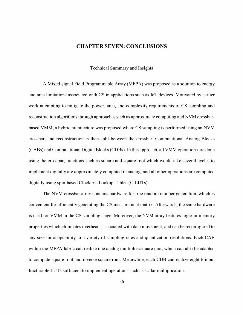
56
CHAPTER SEVEN: CONCLUSIONS
Technical Summary and Insights
A Mixed-signal Field Programmable Array (MFPA) was proposed as a solution to energy
and area limitations associated with CS in applications such as IoT devices. Motivated by earlier
work attempting to mitigate the power, area, and complexity requirements of CS sampling and
reconstruction algorithms through approaches such as approximate computing and NVM crossbar-
based VMM, a hybrid architecture was proposed where CS sampling is performed using an NVM
crossbar, and reconstruction is then split between the crossbar, Computational Analog Blocks
(CABs) and Computational Digital Blocks (CDBs). In this approach, all VMM operations are done
using the crossbar, functions such as square and square root which would take several cycles to
implement digitally are approximately computed in analog, and all other operations are computed
digitally using spin-based Clockless Lookup Tables (C-LUTs).
The NVM crossbar array contains hardware for true random number generation, which is
convenient for efficiently generating the CS measurement matrix. Afterwards, the same hardware
is used for VMM in the CS sampling stage. Moreover, the NVM array features logic-in-memory
properties which eliminates overheads associated with data movement, and can be reconfigured to
any size for adaptability to a variety of sampling rates and quantization resolutions. Each CAB
within the MFPA fabric can realize one analog multiplier/square unit, which can also be adapted
to compute square root and inverse square root. Meanwhile, each CDB can realize eight 6-input
fracturable LUTs sufficient to implement operations such as scalar multiplication.

57
Simulation results with 14 nm CMOS and STT-based 2-terminal spintronic device libraries
indicate that the NVM crossbar allows for a roughly 5× reduction in energy and 32× reduction in
transistor count, compared to CMOS. CABs allow for implementation of an approximate analog
multiplier circuit featuring 32× reduction in transistor count compared to CMOS, as well as single-
cycle implementations of functions which take many cycles to compute digitally. Finally, CDBs
feature 25% reduction in area footprint and 80% reduction in static power consumption compared
to CMOS.
To determine the feasibility of the proposed design in implementing CS reconstruction,
first the error generated by the CABs was injected into three common CS reconstruction algorithms
to assess the impact of this error on the results. In all three cases, the impact of the approximation
error was determined to be negligible, i.e., it had minimal impact on the amount of measurements
necessary to achieve a set reconstruction error of -60 dB.
Finally, a full architecture was proposed specifically for implementation of CS
reconstruction using Approximate Message Passing (AMP). Estimated results indicated a roughly
4.4× reduction in energy usage compared to CMOS, in addition to expected delay reductions by
using CABs, and area savings due to significantly reduced transistor count as compared to CMOS.
The thesis flow is summarized in Fig. 12.
Chapter 3 Chapter 4 Chapter 5 Chapter 6
Fig. 12: Logical organization of this thesis
Propose MFPA Evaluate MFPA component-wise
Evaluate impact of MFPA error
Evaluate MFPA on algorithm scale

58
Technical insights gained from the work presented herein are summarized below:
• Analog computation can offer significant benefits in terms of latency and area,
compared to traditional digital computation.
• Spin-based architectures offer sizable reductions in area due to their ability to be
fabricated vertically onto silicon.
• Spin-based architectures provide significant benefits in terms of energy
consumption, compared to CMOS.
• CS reconstruction algorithms are insensitive to small computation errors. Hence,
schemes leveraging approximate computation for area/power mitigation are
effective for CS.
• The vast majority of energy consumed during CS reconstruction is taken by VMM
operations (about 89% of total energy for the simulation presented in Chapter 6).
The second most energy is taken by ADC/DAC operations (7.8% of total energy).
Thus, the following insights are gained:
o Any approach aiming to minimize CS energy consumption should primarily
target VMM operations.
o While analog computation does introduce extra overheads related to
ADC/DAC, these overheads are tolerable since they are significantly less
than energy reductions that can be attained through more efficient VMM.

59
Scope and Limitations
The obvious limitation of this work is the inability to fabricate the proposed fabric. Thus,
all results presented in Chapter 4 are strictly simulation-based and hence uncertain in regards to
how well they will transfer over to a fabricated chip. Moreover, the algorithm-level results
presented in Chapter 6 are crude estimates due to the fact that no CAD tool is yet available for the
proposed fabric and hence the results had to be computed by hand. While these factors can affect
the accuracy of the results presented, the size of the estimated energy and area gaps between the
proposed fabric and the CMOS equivalent are promising, and indeed suggest that going to the next
step of developing specialized MFPA CAD tools or even developing a fabricated product may be
worthwhile.
Future Work
The advantages of mixed-signal processing, approximate computation, and NVM-based
architectures are promising and open doors for several interesting research questions, including:
• How would the performance of the proposed NVM crossbar array change if the
NVM device were changed to RRAM or PCM? What would be the tradeoffs and
how would the issue of sneak currents factor into this?
• Given the tolerance to approximate computing, what is the optimal bit resolution to
use for the digital computations?

60
• Which CS reconstruction algorithm benefits most from this type of mixed-signal
architecture? For example, would OMP, more heavy in VMM operations, benefit
more from this architecture than AMP?
• How tolerant is the MFPA architecture to process variations in each of the
underlying components?
While in the current stage performance better than CMOS-based digital computation has been
shown, the above questions must be answered before the design can be proven optimal. Only at
this point will the cost of device fabrication be justified.

61
APPENDIX: COPYRIGHT PERMISSIONS

62

63
REFERENCES
[1] J. Huang, M. Parris, J. Lee, and R. F. Demara, "Scalable FPGA-based architecture for DCT
computation using dynamic partial reconfiguration," ACM Transactions on Embedded
Computing Systems, vol. 9, no. 1, p. 9, 2009.
[2] H. Tan and R. F. DeMara, "A multilayer framework supporting autonomous run-time
partial reconfiguration," IEEE Transactions on Very Large Scale Integration (VLSI)
Systems, vol. 16, no. 5, pp. 504-516, 2008.
[3] S. Salehi, R. Zand, and R. F. DeMara, "Clockless Spin-based Look-Up Tables with Wide
Read Margin," in Proceedings of the 2019 on Great Lakes Symposium on VLSI, 2019:
ACM, pp. 363-366.
[4] R. A. Ashraf and R. F. DeMara, "Scalable FPGA refurbishment using netlist-driven
evolutionary algorithms," IEEE Transactions on Computers, vol. 62, no. 8, pp. 1526-1541,
2013.
[5] R. B. Wunderlich, F. Adil, and P. Hasler, "Floating gate-based field programmable mixed-
signal array," IEEE Transactions on Very Large Scale Integration Systems, vol. 21, no. 8,
pp. 1496-1505, 2012.
[6] Y. Huang, "Hybrid Analog-Digital Co-Processing for Scientific Computation," Columbia
University, 2018.

64
[7] B. Rumberg and D. W. Graham, "A low-power field-programmable analog array for
wireless sensing," in Sixteenth International Symposium on Quality Electronic Design,
2015: IEEE, pp. 542-546.
[8] J. C. Kemerling, R. Greenwell, and B. Bharath, "Analog-and mixed-signal fabrics,"
Proceedings of the IEEE, vol. 103, no. 7, pp. 1087-1101, 2015.
[9] A. Septimus and R. Steinberg, "Compressive sampling hardware reconstruction," in
Proceedings of 2010 IEEE International Symposium on Circuits and Systems, 2010: IEEE,
pp. 3316-3319.
[10] S. Salehi, A. Zaeemzadeh, A. Tatulian, N. Rahnavard, and R. F. DeMara, "MRAM-based
Stochastic Oscillators for Adaptive Non-Uniform Sampling of Sparse Signals in IoT
Applications," in Symposium on VLSI Circuits, 2019.
[11] R. Chartrand, "Fast algorithms for nonconvex compressive sensing: MRI reconstruction
from very few data," in 2009 IEEE International Symposium on Biomedical Imaging:
From Nano to Macro, 2009: IEEE, pp. 262-265.
[12] A. Zaeemzadeh, M. Joneidi, and N. Rahnavard, "Adaptive non-uniform compressive
sampling for time-varying signals," in 2017 51st Annual Conference on Information
Sciences and Systems (CISS), 2017: IEEE, pp. 1-6.
[13] E. C. Marques, N. Maciel, L. Naviner, H. Cai, and J. Yang, "A review of sparse recovery
algorithms," IEEE Access, vol. 7, pp. 1300-1322, 2018.
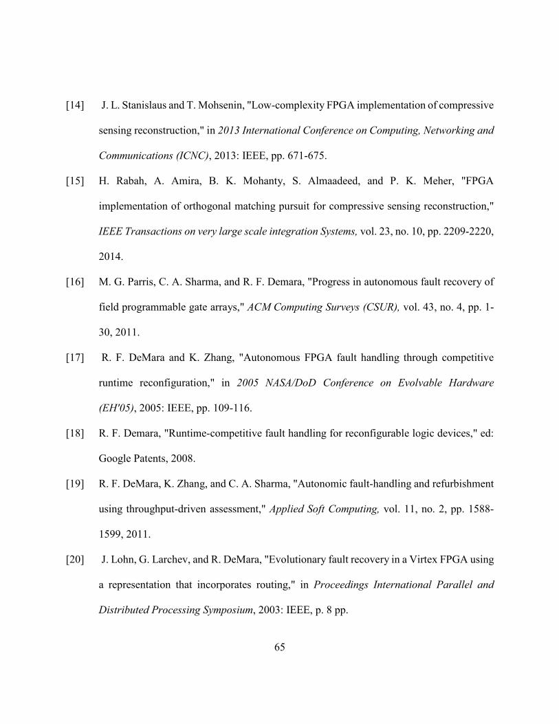
65
[14] J. L. Stanislaus and T. Mohsenin, "Low-complexity FPGA implementation of compressive
sensing reconstruction," in 2013 International Conference on Computing, Networking and
Communications (ICNC), 2013: IEEE, pp. 671-675.
[15] H. Rabah, A. Amira, B. K. Mohanty, S. Almaadeed, and P. K. Meher, "FPGA
implementation of orthogonal matching pursuit for compressive sensing reconstruction,"
IEEE Transactions on very large scale integration Systems, vol. 23, no. 10, pp. 2209-2220,
2014.
[16] M. G. Parris, C. A. Sharma, and R. F. Demara, "Progress in autonomous fault recovery of
field programmable gate arrays," ACM Computing Surveys (CSUR), vol. 43, no. 4, pp. 1-
30, 2011.
[17] R. F. DeMara and K. Zhang, "Autonomous FPGA fault handling through competitive
runtime reconfiguration," in 2005 NASA/DoD Conference on Evolvable Hardware
(EH'05), 2005: IEEE, pp. 109-116.
[18] R. F. Demara, "Runtime-competitive fault handling for reconfigurable logic devices," ed:
Google Patents, 2008.
[19] R. F. DeMara, K. Zhang, and C. A. Sharma, "Autonomic fault-handling and refurbishment
using throughput-driven assessment," Applied Soft Computing, vol. 11, no. 2, pp. 1588-
1599, 2011.
[20] J. Lohn, G. Larchev, and R. DeMara, "Evolutionary fault recovery in a Virtex FPGA using
a representation that incorporates routing," in Proceedings International Parallel and
Distributed Processing Symposium, 2003: IEEE, p. 8 pp.

66
[21] K. Zhang, R. F. DeMara, and C. A. Sharma, "Consensus-based evaluation for fault
isolation and on-line evolutionary regeneration," in International Conference on Evolvable
Systems, 2005: Springer, pp. 12-24.
[22] S. C. Smith, R. F. DeMara, J. S. Yuan, D. Ferguson, and D. Lamb, "Optimization of NULL
convention self-timed circuits," Integration, vol. 37, no. 3, pp. 135-165, 2004.
[23] W. Kuang, P. Zhao, J. S. Yuan, and R. F. DeMara, "Design of asynchronous circuits for
high soft error tolerance in deep submicrometer CMOS circuits," IEEE transactions on
very large scale integration (VLSI) systems, vol. 18, no. 3, pp. 410-422, 2009.
[24] K. Zhang, G. Bedette, and R. F. DeMara, "Triple modular redundancy with standby
(TMRSB) supporting dynamic resource reconfiguration," in 2006 IEEE Autotestcon, 2006:
IEEE, pp. 690-696.
[25] R. Al-Haddad, R. Oreifej, R. A. Ashraf, and R. F. DeMara, "Sustainable modular adaptive
redundancy technique emphasizing partial reconfiguration for reduced power
consumption," International Journal of Reconfigurable Computing, vol. 2011, 2011.
[26] A. Roohi, R. F. DeMara, and N. Khoshavi, "Design and evaluation of an ultra-area-efficient
fault-tolerant QCA full adder," Microelectronics Journal, vol. 46, no. 6, pp. 531-542, 2015.
[27] A. Roohi, R. Zand, and R. F. DeMara, "A tunable majority gate-based full adder using
current-induced domain wall nanomagnets," IEEE Transactions on Magnetics, vol. 52, no.
8, pp. 1-7, 2016.

67
[28] A. Roohi, R. Zand, D. Fan, and R. F. DeMara, "Voltage-based concatenatable full adder
using spin hall effect switching," IEEE Transactions on Computer-Aided Design of
Integrated Circuits and Systems, vol. 36, no. 12, pp. 2134-2138, 2017.
[29] S. Salehi, D. Fan, and R. F. Demara, "Survey of STT-MRAM cell design strategies:
Taxonomy and sense amplifier tradeoffs for resiliency," ACM Journal on Emerging
Technologies in Computing Systems (JETC), vol. 13, no. 3, pp. 1-16, 2017.
[30] S. Salehi, M. B. Mashhadi, A. Zaeemzadeh, N. Rahnavard, and R. F. DeMara, "Energy-
Aware Adaptive Rate and Resolution Sampling of Spectrally Sparse Signals Leveraging
VCMA-MTJ Devices," IEEE Journal on Emerging and Selected Topics in Circuits and
Systems, vol. 8, no. 4, pp. 679-692, 2018.
[31] L. Wei et al., "13.3 A 7Mb STT-MRAM in 22FFL FinFET Technology with 4ns Read
Sensing Time at 0.9 V Using Write-Verify-Write Scheme and Offset-Cancellation Sensing
Technique," in 2019 IEEE International Solid-State Circuits Conference-(ISSCC), 2019:
IEEE, pp. 214-216.
[32] R. Zand, A. Roohi, S. Salehi, and R. F. DeMara, "Scalable adaptive spintronic
reconfigurable logic using area-matched MTJ design," IEEE Transactions on Circuits and
Systems II: Express Briefs, vol. 63, no. 7, pp. 678-682, 2016.
[33] R. Zand, A. Roohi, D. Fan, and R. F. DeMara, "Energy-efficient nonvolatile reconfigurable
logic using spin hall effect-based lookup tables," IEEE Transactions on Nanotechnology,
vol. 16, no. 1, pp. 32-43, 2016.

68
[34] S. Salehi, R. Zand, A. Zaeemzadeh, N. Rahnavard, and R. F. DeMara, "AQuRate: MRAM-
based Stochastic Oscillator for Adaptive Quantization Rate Sampling of Sparse Signals,"
in Proceedings of the 2019 on Great Lakes Symposium on VLSI, 2019: ACM, pp. 359-362.
[35] A. Tatulian, S. Salehi, and R. F. DeMara, "Mixed-Signal Spin/Charge Reconfigurable
Array for Energy-Aware Compressive Signal Processing," in 2019 International
Conference on ReConFigurable Computing and FPGAs (ReConFig), 2019: IEEE, pp. 1-
8.
[36] C. Schlottmann and P. Hasler, "FPAA empowering cooperative analog-digital signal
processing," in 2012 IEEE International Conference on Acoustics, Speech and Signal
Processing (ICASSP), 2012: IEEE, pp. 5301-5304.
[37] S. George et al., "A programmable and configurable mixed-mode FPAA SoC," IEEE
Transactions on Very Large Scale Integration Systems, vol. 24, no. 6, pp. 2253-2261, 2016.
[38] Y. Choi, Y. Lee, S.-H. Baek, S.-J. Lee, and J. Kim, "CHIMERA: A Field-Programmable
Mixed-Signal IC With Time-Domain Configurable Analog Blocks," IEEE Journal of
Solid-State Circuits, vol. 53, no. 2, pp. 431-444, 2017.
[39] S. D. Pyle, V. Thangavel, S. M. Williams, and R. F. DeMara, "Self-Scaling Evolution of
analog computation circuits with digital accuracy refinement," in 2015 NASA/ESA
Conference on Adaptive Hardware and Systems (AHS), 2015: IEEE, pp. 1-8.
[40] R. S. Oreifej, R. N. Al-Haddad, H. Tan, and R. F. DeMara, "Layered approach to intrinsic
evolvable hardware using direct bitstream manipulation of Virtex II Pro devices," in 2007

69
International Conference on Field Programmable Logic and Applications, 2007: IEEE,
pp. 299-304.
[41] R. S. Oreifej, C. A. Sharma, and R. F. DeMara, "Expediting GA-based evolution using
group testing techniques for reconfigurable hardware," in 2006 IEEE International
Conference on Reconfigurable Computing and FPGA's (ReConFig 2006), 2006: IEEE, pp.
1-8.
[42] V. Thangavel, Z.-X. Song, and R. F. DeMara, "Intrinsic evolution of truncated Puiseux
series on a mixed-signal field-programmable soc," IEEE Access, vol. 4, pp. 2863-2872,
2016.
[43] S. Park, J. Kim, and S. Yoon, "Energy-aware Placement for SRAM-NVM Hybrid FPGAs."
[44] J. Cong and B. Xiao, "FPGA-RPI: A novel FPGA architecture with RRAM-based
programmable interconnects," IEEE Transactions on Very Large Scale Integration (VLSI)
Systems, vol. 22, no. 4, pp. 864-877, 2013.
[45] K. Huang, R. Zhao, W. He, and Y. Lian, "High-density and high-reliability nonvolatile
field-programmable gate array with stacked 1D2R RRAM array," IEEE Transactions on
Very Large Scale Integration (VLSI) Systems, vol. 24, no. 1, pp. 139-150, 2015.
[46] X. Tang, P.-E. Gaillardon, and G. De Micheli, "A high-performance low-power near-Vt
RRAM-based FPGA," in 2014 International Conference on Field-Programmable
Technology (FPT), 2014: IEEE, pp. 207-214.

70
[47] Y. Y. Liauw, Z. Zhang, W. Kim, A. El Gamal, and S. S. Wong, "Nonvolatile 3D-FPGA
with monolithically stacked RRAM-based configuration memory," in 2012 IEEE
International Solid-State Circuits Conference, 2012: IEEE, pp. 406-408.
[48] S. Paul, S. Mukhopadhyay, and S. Bhunia, "Hybrid CMOS-STTRAM non-volatile FPGA:
Design challenges and optimization approaches," in 2008 IEEE/ACM International
Conference on Computer-Aided Design, 2008: IEEE, pp. 589-592.
[49] K. Jo, K. Cho, and H. Yoon, "Variation-tolerant and low power look-up table (LUT) using
spin-torque transfer magnetic RAM for non-volatile field programmable gate array
(FPGA)," in 2016 International SoC Design Conference (ISOCC), 2016: IEEE, pp. 101-
102.
[50] J. Kim, K. T. Kim, and E.-Y. Chung, "CAD Tool Flow for Variation-Tolerant Non-
Volatile STT-MRAM LUT based FPGA," in Proceedings of the 2018 7th International
Conference on Software and Computer Applications, 2018: ACM, pp. 312-316.
[51] Y. Chen, J. Zhao, and Y. Xie, "3D-NonFAR: Three-dimensional non-volatile FPGA
architecture using phase change memory," in Proceedings of the 16th ACM/IEEE
international symposium on Low power electronics and design, 2010, pp. 55-60.
[52] P.-E. Gaillardon et al., "Phase-change-memory-based storage elements for configurable
logic," in 2010 International Conference on Field-Programmable Technology, 2010:
IEEE, pp. 17-20.
[53] K. Huang, Y. Ha, R. Zhao, A. Kumar, and Y. Lian, "A low active leakage and high
reliability phase change memory (PCM) based non-volatile FPGA storage element," IEEE

71
Transactions on Circuits and Systems I: Regular Papers, vol. 61, no. 9, pp. 2605-2613,
2014.
[54] M. Fardad, S. M. Sayedi, and E. Yazdian, "A Low-Complexity Hardware for Deterministic
Compressive Sensing Reconstruction," IEEE Transactions on Circuits and Systems I:
Regular Papers, vol. 65, no. 10, pp. 3349-3361, 2018.
[55] S. Leitner, H. Wang, and S. Tragoudas, "Design of scalable hardware-efficient
compressive sensing image sensors," IEEE Sensors Journal, vol. 18, no. 2, pp. 641-651,
2017.
[56] A. Jafari, A. Page, C. Sagedy, E. Smith, and T. Mohsenin, "A low power seizure detection
processor based on direct use of compressively-sensed data and employing a deterministic
random matrix," in 2015 IEEE Biomedical Circuits and Systems Conference (BioCAS),
2015: IEEE, pp. 1-4.
[57] Y. Massoud, F. Xiong, and S. Smaili, "A memristor-based random modulator for
compressive sensing systems," in 2012 IEEE International Symposium on Circuits and
Systems, 2012: IEEE, pp. 2445-2448.
[58] F. Qian, Y. Gong, G. Huang, M. Anwar, and L. Wang, "Exploiting memristors for
compressive sampling of sensory signals," IEEE Transactions on Very Large Scale
Integration (VLSI) Systems, vol. 26, no. 12, pp. 2737-2748, 2018.
[59] S. P. Kadiyala, V. K. Pudi, and S.-K. Lam, "Approximate compressed sensing for
hardware-efficient image compression," in 2017 30th IEEE International System-on-Chip
Conference (SOCC), 2017: IEEE, pp. 340-345.

72
[60] F. Ren, R. Dorrace, W. Xu, and D. Marković, "A single-precision compressive sensing
signal reconstruction engine on FPGAs," in 2013 23rd International Conference on Field
programmable Logic and Applications, 2013: IEEE, pp. 1-4.
[61] S. Liu, A. Ren, Y. Wang, and P. K. Varshney, "Ultra-fast robust compressive sensing
based on memristor crossbars," in 2017 IEEE International Conference on Acoustics,
Speech and Signal Processing (ICASSP), 2017: IEEE, pp. 1133-1137.
[62] M. Le Gallo, A. Sebastian, G. Cherubini, H. Giefers, and E. Eleftheriou, "Compressed
sensing with approximate message passing using in-memory computing," IEEE
Transactions on Electron Devices, vol. 65, no. 10, pp. 4304-4312, 2018.
[63] A. Kulkarni and T. Mohsenin, "Low overhead architectures for OMP compressive sensing
reconstruction algorithm," IEEE Transactions on Circuits and Systems I: Regular Papers,
vol. 64, no. 6, pp. 1468-1480, 2017.
[64] D. Bellasi, M. Crescentini, D. Cristaudo, A. Romani, M. Tartagni, and L. Benini, "A
Broadband Multi-Mode Compressive Sensing Current Sensor SoC in 0.16$\mu $ m
CMOS," IEEE Transactions on Circuits and Systems I: Regular Papers, vol. 66, no. 1, pp.
105-118, 2018.
[65] D. Bortolotti et al., "Approximate compressed sensing: ultra-low power biosignal
processing via aggressive voltage scaling on a hybrid memory multi-core processor," in
Proceedings of the 2014 international symposium on Low power electronics and design,
2014: ACM, pp. 45-50.

73
[66] S. Salehi and R. F. DeMara, "SLIM-ADC: Spin-based Logic-In-Memory Analog to Digital
Converter leveraging SHE-enabled Domain Wall Motion devices," Microelectronics
Journal, vol. 81, pp. 137-143, 2018.
[67] R. F. DeMara and D. I. Moldovan, "The SNAP-1 parallel AI prototype," IEEE
Transactions on Parallel and Distributed Systems, vol. 4, no. 8, pp. 841-854, 1993.
[68] "22nm Predictive Technology Model (PTM)." http://ptm.asu.edu/ (accessed March 2,
2020).
[69] J. Kim, A. Chen, B. Behin-Aein, S. Kumar, J.-P. Wang, and C. H. Kim, "A technology-
agnostic MTJ SPICE model with user-defined dimensions for STT-MRAM scalability
studies," in 2015 IEEE custom integrated circuits conference (CICC), 2015: IEEE, pp. 1-
4.
[70] W. Kang, Y. Ran, Y. Zhang, W. Lv, and W. Zhao, "Modeling and exploration of the
voltage-controlled magnetic anisotropy effect for the next-generation low-power and high-
speed MRAM applications," IEEE Transactions on Nanotechnology, vol. 16, no. 3, pp.
387-395, 2017.
[71] K. Y. Camsari, S. Salahuddin, and S. Datta, "Implementing p-bits with embedded MTJ,"
IEEE Electron Device Letters, vol. 38, no. 12, pp. 1767-1770, 2017.
[72] Y. Oike and A. El Gamal, "CMOS image sensor with per-column ΣΔ ADC and
programmable compressed sensing," IEEE Journal of Solid-State Circuits, vol. 48, no. 1,
pp. 318-328, 2012.

74
[73] F. Qian, Y. Gong, G. Huang, K. Ahi, M. Anwar, and L. Wang, "A memristor-based
compressive sensing architecture," in 2016 IEEE/ACM International Symposium on
Nanoscale Architectures (NANOARCH), 2016: IEEE, pp. 109-114.
[74] A. Biswas and A. P. Chandrakasan, "A 0.36 V 128Kb 6T SRAM with energy-efficient
dynamic body-biasing and output data prediction in 28nm FDSOI," in ESSCIRC
Conference 2016: 42nd European Solid-State Circuits Conference, 2016: IEEE, pp. 433-
436.
[75] I. Hassoune, D. Flandre, and I. O'Connor, "ULPFA: A new efficient design of a power-
aware full adder," IEEE Transactions on Circuits and Systems I: Regular Papers, vol. 57,
no. 8, pp. 2066-2074, 2008.
[76] A. T. Mahani and P. Keshavarzian, "A novel energy-efficient and high speed full adder
using CNTFET," Microelectronics Journal, vol. 61, pp. 79-88, 2017.
[77] H. Jiang, C. Liu, F. Lombardi, and J. Han, "Low-power approximate unsigned multipliers
with configurable error recovery," IEEE Transactions on Circuits and Systems I: Regular
Papers, vol. 66, no. 1, pp. 189-202, 2018.
[78] J. Lu, H. Zhang, and H. Meng, "Novel hardware architecture of sparse recovery based on
FPGAs," in 2010 2nd International Conference on Signal Processing Systems, 2010, vol.
1: IEEE, pp. V1-302-V1-306.
[79] L. Bai, P. Maechler, M. Muehlberghuber, and H. Kaeslin, "High-speed compressed
sensing reconstruction on FPGA using OMP and AMP," in 2012 19th IEEE International
Conference on Electronics, Circuits, and Systems (ICECS 2012), 2012: IEEE, pp. 53-56.

75
[80] A. Hasnat, T. Bhattacharyya, A. Dey, S. Halder, and D. Bhattacharjee, "A fast FPGA based
architecture for computation of square root and inverse square root," in 2017 Devices for
Integrated Circuit (DevIC), 2017: IEEE, pp. 383-387.