mic2619 march02
TRANSCRIPT

MIC2619 1.2MHz PWM Boost Converter
with OVP
Micrel Inc. • 2180 Fortune Drive • San Jose, CA 95131 • USA • tel +1 (408) 944-0800 • fax + 1 (408) 474-1000 • http://www.micrel.com
March 2010 M9999-030410-A
General Description The MIC2619 is a 1.2MHz pulse width modulated (PWM) step-up switching regulator that is optimized for low power, high output voltage applications. With a maximum output voltage of 35V, and a switch current of over 350mA, the MIC2619 can easily supply most high voltage bias applications, such as TV tuners. The MIC2619 implements a constant frequency 1.2MHz PWM current-mode control scheme. The high frequency PWM operation saves board space by reducing external component sizes. The additional benefit of the constant frequency PWM control scheme as opposed to variable frequency control schemes is lower output noise and smaller input ripple injected back to the battery source. The MIC2619 has programmable overvoltage protection to ensure output protection in case of fault condition. The MIC2619 is available in a low profile Thin SOT-23 6-pin package. The MIC2619 has a junction temperature range of –40°C to +125°C. All support documentation can be found on Micrel’s web site at: www.micrel.com.
Features • 2.8V to 6.5V Input Voltage • 350mA Switch Current • Output Voltage up to 35V • 1.2MHz PWM Operation • 1.265V Feedback Voltage • Programmable Over-Voltage Protection (OVP) • <1% Line Regulation • <1µA Shutdown Current • Over-Temperature Protection • Under-Voltage Lock Out (UVLO) • Low Profile Thin SOT-23-6 Package • –40°C to +125°C Junction Temperature Range Applications • Bias Supply Applications:
- Tuner Varactor Bias - High Voltage Bias Supplies - Avalanche Photo Diode - High Voltage Display Bias
• DSL/Broadband applications • Constant Current Power Supplies
_________________________________________________________________________________________________________________________
Typical Application
1.2MHz Boost Converter with OVP in Thin SOT-23-6
Micrel, Inc. MIC2619
March 2010 2 M9999-030410-A
Ordering Information Part Number Marking(1) Overvoltage
Protection Junction Temp.
Range Package Lead Finish
MIC2619YD6 2619 Programmable -40°C to +125°C Thin SOT-23-6 Lead Free Note: 1. Under bar( ) symbol may not be to scale.
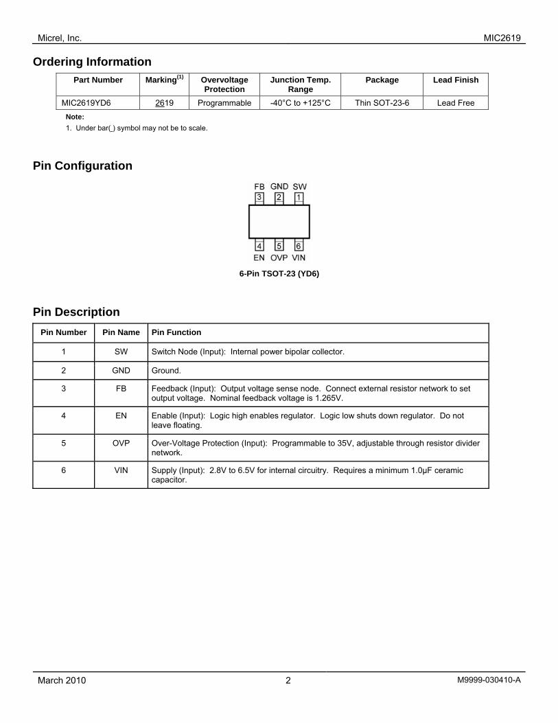
Pin Configuration
6-Pin TSOT-23 (YD6)
Pin Description Pin Number Pin Name Pin Function
1 SW Switch Node (Input): Internal power bipolar collector.
2 GND Ground.
3 FB Feedback (Input): Output voltage sense node. Connect external resistor network to set output voltage. Nominal feedback voltage is 1.265V.
4 EN Enable (Input): Logic high enables regulator. Logic low shuts down regulator. Do not leave floating.
5 OVP Over-Voltage Protection (Input): Programmable to 35V, adjustable through resistor divider network.
6 VIN Supply (Input): 2.8V to 6.5V for internal circuitry. Requires a minimum 1.0µF ceramic capacitor.

Micrel, Inc. MIC2619
March 2010 3 M9999-030410-A
Absolute Maximum Ratings(1) Supply Voltage (VIN) .........................................................7V Switch Voltage (VSW)....................................... –0.3V to 40V Enable Pin Voltage (VEN)..................................... –0.3 to VIN Feedback Voltage (VFB), (VOVP)........................................6V Ambient Storage Temperature (TS)...........–65°C to +150°C ESD Rating (3) ................................................................. 2kV
Operating Ratings(2) Supply Voltage (VIN)......................................... 2.8V to 6.5V Output Voltage (VOUT) .......................................... VIN to 35V Junction Temperature Range (TJ).............–40°C to +125°C Package Thermal Impedance Thin SOT-23-6 (θJA).........................................177°C/W
Electrical Characteristics (4) TA = 25°C, VIN = VEN = 3.6V, VOUT = 10V, IOUT = 10mA, unless otherwise noted. Bold values indicate –40°C ≤ TJ ≤125°C.
Parameter Condition Min Typ Max Units
Supply Voltage Range 2.8 6.5 V
Under Voltage Lockout 1.8 2.1 2.4 V
Quiescent Current VFB > 1.265V, (not switching) 2.1 5 mA
Shutdown Current VEN = 0V 0.04 1 µA
Feedback Voltage 1.227 1.265 1.303 V
Feedback Input Current VFB = 1.265V -450 nA
Line Regulation 2.8V ≤ VIN ≤ 6.5V 0.2 1 %
Load Regulation 5mA ≤ IOUT ≤ 20mA 0.3 %
Maximum Duty Cycle 85 90 %
Switch Current Limit VIN = 3.6V(5) 350 mA
Switch Saturation Voltage VIN = 3.6V, ISW = 300mA 400 mV
Switch Leakage Current VEN = 0V, VSW = 10V 0.01 1 µA
TURN ON 1.5 Enable Threshold
TURN OFF 0.4 V
Enable Pin Current VEN = 6.5V 14 40 µA
Oscillator Frequency 1.2 MHz
Overvoltage Protection 1.202 1.265 1.328 V
OVP Input Current VOVP = 1.265V –200 nA
150 °C Overtemperature Threshold Shutdown Hysteresis 10 °C
Notes:
1. Absolute maximum ratings indicate limits beyond which damage to the component may occur. Electrical specifications do not apply when operating the device outside of its operating ratings. The maximum allowable power dissipation is a function of the maximum junction temperature, TJ(max), the junction-to-ambient thermal resistance, θJA, and the ambient temperature, TA. The maximum allowable power dissipation will result in excessive die temperature, and the regulator will go into thermal shutdown.
2. This device is not guaranteed to operate beyond its specified operating ratings.
3. Devices are inherently ESD sensitive. Handling precautions required. Human body model: 1.5kΩ in series with 100pF.
4. Specification for packaged product only.
5. Guaranteed by design.

Micrel, Inc. MIC2619
March 2010 4 M9999-030410-A
Typical Characteristics
Efficiency VOUT = 5V
0%
10%20%
30%40%
50%
60%70%
80%90%
100%
0 50 100 150 200LOAD CURRENT (mA)
EFFI
CIE
NC
Y (%
)
VIN=3V
VIN=3.6VVIN=4.2V
L = 10µHC = 1µF
Efficiency VOUT = 10V
0%
10%
20%
30%
40%
50%
60%
70%
80%
90%
0 20 40 60 80 100LOAD CURRENT (mA)
EFFI
CIE
NC
Y (%
)
VIN=3.3V
VIN=5V
L = 10µHC = 1µF
Efficiency VOUT = 12V
0%
10%
20%
30%
40%
50%
60%
70%
80%
90%
0 20 40 60 80LOAD CURRENT (mA)
EFFI
CIE
NC
Y (%
)
VIN=3.3VVIN=5V
L = 10µHC = 1µF
Frequencyvs. Input Voltage
0.900.951.001.051.101.151.201.251.301.351.401.451.50
3 3.5 4 4.5 5 5.5 6 6.5INPUT VOLTAGE (V)
FREQ
UEN
CY
(MH
z)
VOU T = 12VL = 10µHC = 1µFILOAD = 40mA
Switch Current Limitvs. Input Voltage
200
300
400
500
600
700
800
900
1000
1100
3 3.5 4 4.5 5 5.5 6 6.5INPUT VOLTAGE (V)
CU
RR
ENT
LIM
IT (m
A)
VOUT = 12VL = 10µHC = 1µF
Efficiency VOUT = 35V
0%
10%
20%
30%
40%
50%
60%
70%
0 4 8 12 16LOAD CURRENT (mA)
EFFI
CIE
NC
Y (%
)
VIN=5V
VIN=6.5V
L = 10µHC = 1µF
Load Regulation (VOUT=35V)
34.5
34.6
34.7
34.8
34.9
35.0
35.1
35.2
35.3
35.4
35.5
0 2 4 6 8 10 12LOAD CURRENT (mA)
OU
TPU
T VO
LTA
GE
(V)
VIN = 5VL = 10µHC = 1µF
Load Regulation (VOUT=10V)
9.90
9.929.94
9.969.98
10.00
10.0210.04
10.0610.08
10.10
0 10 20 30 40 50 60 70LOAD CURRENT (mA)
OU
TPU
T VO
LTA
GE
(V)
VIN = 3.6VL = 10µHC = 1µF
Line Regulation (VOUT=12V)
11.80
11.8411.88
11.92
11.96
12.0012.04
12.08
12.1212.16
12.20
3 3.5 4 4.5 5 5.5 6 6.5INPUT VOLTAGE (V)
OU
TPU
T VO
LTA
GE
(V)
IOU T = 40mAL = 10µHC = 1µF
Line Regulation (VOUT=35V)
34.5
34.6
34.7
34.8
34.935.0
35.1
35.2
35.3
35.4
35.5
4.5 4.9 5.3 5.7 6.1 6.5INPUT VOLTAGE (V)
OU
TPU
T VO
LTA
GE
(V)
IOUT = 10mAL = 10µHC = 1µF
Switch Current Limitvs. T emperature
0
100
200
300
400
500
600
700
800
900
-40 -20 0 20 40 60 80 100 120TEMPERATURE (°C)
CU
RR
ENT
LIM
IT (m
A)
VIN = 3.6VVOU T = 12VL = 10µHC = 1µF
Quiescent Currentvs. Input Voltage
0.500.751.001.251.501.752.002.252.502.753.003.253.50
3.0 3.5 4.0 4.5 5.0 5.5 6.0 6.5INPUT VOLTAGE (V)
QU
IESC
ENT
CU
RR
ENT
(mA
)
VFB = 3VNo Switching

Micrel, Inc. MIC2619
March 2010 5 M9999-030410-A
Typical Characteristics (Continued)
Feedback Voltagevs. T emperature
1.18
1.20
1.22
1.24
1.26
1.28
1.30
1.32
1.34
-40 -20 0 20 40 60 80 100 120TEMPERATURE (°C)
FEED
BA
CK
VO
LTA
GE
(V)
VIN = 3.6VVOU T = 12VIOU T = 25mAL = 10µHC = 1µF
Switching Frequencyvs. T emperature
0.90
0.951.00
1.05
1.10
1.151.20
1.25
1.301.35
1.40
-40 -20 0 20 40 60 80 100 120Temperature (°C)
SWIT
CH
ING
FR
EQU
ENC
Y (M
Hz)
VIN = 3.6VVOUT = 12VIOUT = 25mAL = 10µHC = 1µF

Micrel, Inc. MIC2619
March 2010 6 M9999-030410-A
Functional Characteristics

Micrel, Inc. MIC2619
March 2010 7 M9999-030410-A
Functional Characteristics (Continued)

Micrel, Inc. MIC2619
March 2010 8 M9999-030410-A
Functional Diagram
MIC2619 Block Diagram
Functional Description The MIC2619 is a constant frequency, PWM current mode boost regulator. It is composed of an oscillator, slope compensation ramp generator, current amplifier, gm error amplifier, PWM generator, and bipolar output transistor. The oscillator generates a 1.2MHz clock which triggers the PWM generator to turn on the output transistor and resets the slope compensation ramp generator. The current amplifier is used to measure switch current by amplifying the voltage signal from the internal sense resistor. The output of the current amplifier is summed with the output of the slope compensation ramp generator. This summed current-loop signal is then fed to one of the inputs of the PWM generator. The gm error amplifier measures the feedback voltage through the external feedback resistors and amplifies the error between the detected signal and the 1.265V reference voltage. The output of the gm error amplifier provides the voltage-loop signal that is fed to the other input of the PWM generator. When the current-loop signal exceeds the voltage loop signal, the PWM generator turns off the bipolar output transistor. The next clock period initiates the next switching cycle, maintaining the constant frequency current-mode PWM control.
VIN VIN provides power to the control and reference circuitry as well as the switch mode regulator MOSFETs. Due to the high speed switching, a 1µF capacitor is recommended as close as possible to the VIN and GND pin.
EN The enable pin provides a logic level control of the output. In the off state, supply current of the device is greatly reduced (typically <0.1µA). Also, in the off state, the output drive is placed in a “tri-stated” condition, where the bipolar output transistor is in an “off” state or non-conducting state.
OVP The OVP pin provides over-voltage protection on the output of the MIC2619. When the OVP circuit is tripped, the output voltage remains at the set OVP voltage. Because the OVP circuit operates at a lower frequency than the feedback circuit, output ripple will be higher while in an OVP state. OVP requires a resistor divider network to the output and GND to set the OVP voltage. If the output voltage overshoots the set OVP voltage, then the MIC2619 OVP circuit will shut off the switch; saving itself and other sensitive circuitry downstream. The accuracy of the OVP pin is ±5% and therefore should be set above the output voltage to ensure noise or other variations will not cause a false triggering of the OVP circuit.

Micrel, Inc. MIC2619
March 2010 9 M9999-030410-A
FB The feedback pin provides the control path to control the output. FB requires a resistor divider network to the output and GND to set the output voltage.
SW The switching pin connects directly to one end of the inductor to VIN and the anode of the Schottky diode to the output. Due to the high switching speed and high
voltage associated with this pin, the switch node should be routed away from sensitive nodes.
GND The ground pin is the ground path for high current PWM mode. The current loop for the power ground should be kept as small as possible.

Micrel, Inc. MIC2619
March 2010 10 M9999-030410-A
Application Information
DC-to-DC PWM Boost Conversion The MIC2619 is a constant-frequency boost converter. It can convert a low DC input voltage to a higher DC output voltage. Figure 1 shows a typical circuit. Boost regulation is achieved by turning on an internal switch, which draws current through the inductor. When the switch turns off, the inductor’s magnetic field collapses. This causes the current to be discharged into the output capacitor through an external Schottky diode (D1). The Functional Characteristics show Input Voltage ripple, Output Voltage ripple, SW Voltage, and Inductor Current for 10mA load current. Regulation is achieved by modulating the pulse width i.e., pulse-width modulation (PWM).
Figure 1. Typical Application Circuit
Duty Cycle Considerations Duty cycle refers to the switch on-to-off time ratio and can be calculated as follows for a boost regulator:
OUT
IN
VV
1D −=
However at light loads, the inductor will completely discharge before the end of a switching cycle. The current in the inductor reaches 0A before the end of the switching cycle. This is known as discontinuous conduction mode (DCM). DCM occurs when:
2
IVV
I PEAK
OUT
INOUT ⋅<
Where
( )
⎟⎟⎠
⎞⎜⎜⎝
⎛⋅
⋅−
=OUT
ININOUTPEAK V
VfL
VVI
In DCM, the duty cycle is smaller than in continuous conduction mode. In DCM the duty cycle is given by:
( )
IN
INOUTOUT
VVVIL2f
D−⋅⋅⋅⋅
=
The duty cycle required for voltage conversion should be less than the maximum duty cycle of 85%. Also, in light load conditions where the input voltage is close to the output voltage, the minimum duty cycle can cause pulse skipping. This is due to the energy stored in the inductor causing the output to slightly overshoot the regulated output voltage. During the next cycle, the error amplifier detects the output as being high and skips the following pulse. This effect can be reduced by increasing the minimum load or by increasing the inductor value. Increasing the inductor value also reduces the peak current.
Input Capacitors A 1µF ceramic capacitor is recommended on the VIN pin for bypassing. Increasing input capacitance will improve performance and provide greater noise immunity. The input capacitor should be as close as possible to the inductor and the MIC2619, with short traces for good noise performance. X5R or X7R dielectrics are recommended for the input capacitor. Y5V dielectrics lose most of their capacitance over temperature and are therefore not recommended. Also, tantalum and electrolytic capacitors alone are not recommended because of their reduced RMS current handling, reliability, and ESR increases.
Output Capacitors Output capacitor selection is also a trade-off between performance, size, and cost. The minimum recommended output capacitor is 1µF. Increasing output capacitance will lead to an improved transient response but also an increase in size and cost. X5R or X7R dielectrics are recommended for the output capacitor. Y5V dielectrics lose most of their capacitance over temperature and are therefore not recommended.
Inductor Inductor selection will be determined by the following (not necessarily in order of importance);
• Inductance • Rated current value • Size requirements • DC resistance (DCR)
The MIC2619 was designed for use with a 10µH inductor. Proper selection should ensure the inductor can handle the maximum average and peak currents required by the load. Maximum current ratings of the inductor are generally given in two methods; permissible DC current and saturation current. Permissible DC current can be rated either for a 40°C temperature rise or a 10 to 20% loss in inductance. Ensure the inductor selected can handle the maximum operating current. When saturation current is specified, make sure that there is enough margin so that the peak current will not
Micrel, Inc. MIC2619
March 2010 11 M9999-030410-A
saturate the inductor. Peak current can be calculated as follows:
⎥⎦
⎤⎢⎣
⎡⎟⎠
⎞⎜⎝
⎛××⋅−
+=Lf2VV1VII INOUT
OUTOUTPEAK
As shown by the previous calculation, the peak inductor current is inversely proportional to the switching frequency and the inductance; the lower the switching frequency or the inductance the higher the peak current. As input voltage increases the peak current also increases. The size of the inductor depends on the requirements of the application. DC resistance (DCR) is also important. While DCR is inversely proportional to size, DCR can represent a significant efficiency loss. Refer to the Efficiency Considerations. To maintain stability, increasing inductor size will have to be met with an increase in output capacitance. This is due to the unavoidable “right half plane zero” effect for the continuous current boost converter topology. The frequency at which the right half plane zero occurs can be calculated as follows:
π2ILV
VFrequency
OUTOUT
2IN
⋅⋅⋅=
The right half plane zero has the undesirable effect of increasing gain, while decreasing phase. This requires that the loop gain is rolled off before this has significant effect on the total loop response. This can be accomplished by either reducing inductance (increasing RHPZ frequency) or increasing the output capacitor value (decreasing loop gain).
Diode Selection The MIC2619 requires an external diode for operation. A Schottky diode is recommended for most applications due to their lower forward voltage drop and reverse recovery time. Ensure the diode selected can deliver the peak inductor current and the maximum reverse voltage is rated greater than the output voltage.
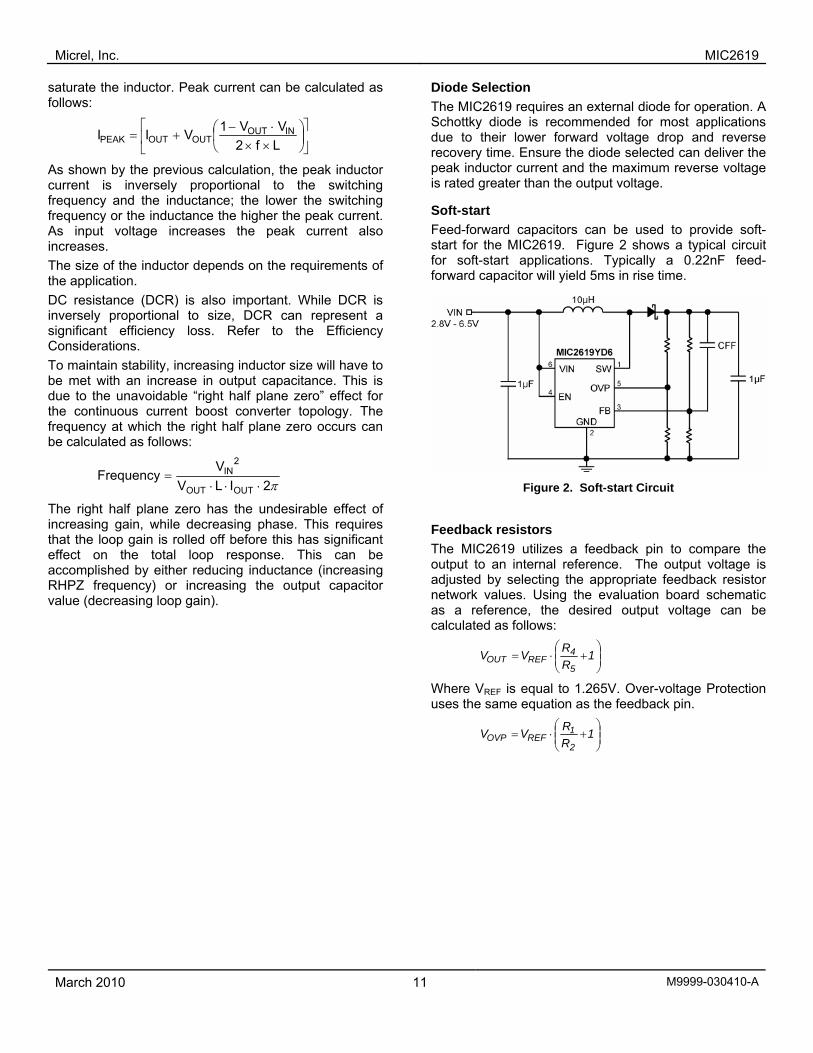
Soft-start Feed-forward capacitors can be used to provide soft-start for the MIC2619. Figure 2 shows a typical circuit for soft-start applications. Typically a 0.22nF feed-forward capacitor will yield 5ms in rise time.
Figure 2. Soft-start Circuit
Feedback resistors The MIC2619 utilizes a feedback pin to compare the output to an internal reference. The output voltage is adjusted by selecting the appropriate feedback resistor network values. Using the evaluation board schematic as a reference, the desired output voltage can be calculated as follows:
⎟⎟⎠
⎞⎜⎜⎝
⎛+⋅= 1
RRVV
5
4REFOUT
Where VREF is equal to 1.265V. Over-voltage Protection uses the same equation as the feedback pin.
⎟⎟⎠
⎞⎜⎜⎝
⎛+⋅= 1
RRVV
2
1REFOVP

Micrel, Inc. MIC2619
March 2010 12 M9999-030410-A
MIC2619 Evaluation Board Schematic
Bill of Materials Item Part Number Manufacturer Description Qty.
C1608X5R1A105K TDK(1) Capacitor, 1.0µF, 10V, X5R, 0603 size GRM185R61A105KE36D Murata(2) Capacitor, 1.0µF, 10V, X5R, 0603 size
C1
0603ZD105KT2A AVX(3) Capacitor, 1.0µF, 10V, X5R, 0603 size
1
C2 TAJA106M010R AVX Capacitor, 10.0µF, 10V, A Case 1 C1608X7R11H223K TDK Capacitor, 22nF, 50V, X7R, 0603 size GRM188R71H223KA01D Murata Capacitor, 22nF, 50V, X7R, 0603 size
C3
06035C223JAT2A AVX Capacitor, 22nF, 50V, X7R, 0603 size
1
08055D105MAT2A AVX Capacitor, 1.0µF, 50V, X5R, 0805 size GRM21BR71H105KA12L Murata Capacitor, 1.0µF, 50V, X5R, 0805 size
C4
CL21B105KBFNNNE Samsung(4) Capacitor, 1.0µF, 50V, X7R, 0805 size
1
SK14 MCC(5) Schottky Diode, 1A, 40V D1 B140/B Diode, Inc.(6) Schottky Diode, 1A, 40V
1
C1G22L100MNE Samsung Inductor, 10.0µH, 0.8A, 2.5 x 2.0 x 1.0mm VLF3012ST-100MR59 TDK Inductor, 10.0µH, 0.59A, 2.8 x 3.0 x 1.2mm
L1
LQH32PN100MN0L Murata Inductor, 10.0µH, 0.7A, 3.2 x 2.5 x 1.55mm
1
R1 CRCW0603267KFKEA Vishay(7) Resistor, 267kΩ, 1%, 1/16W, 0603 size 1 R2, R5 CRCW060310K0FKEA Vishay Resistor, 10kΩ, 1%, 1/16W, 0603 size 2 R3 CRCW0603100KFKEA Vishay Resistor, 100kΩ, 1%, 1/16W, 0603 size 1 R4 CRCW0603226KFKEA Vishay Resistor, 226kΩ, 1%, 1/16W, 0603 size 1 U1 MIC2619YD6 Micrel, Inc.(8) 1.2MHz PWM Boost Converter with OVP 1
Notes: 1. TDK: www.tdk.com 2. Murata: www.murata.com 3. AVX: www.avx.com 4. Samsung: www.sem.samsung.com 5. MCC: www.mccsemi.com 6. Diode, Inc.: www.diodes.com 7. Vishay: www.vishay.com 8. Micrel, Inc.: www.micrel.com

Micrel, Inc. MIC2619
March 2010 13 M9999-030410-A
Recommended Layout
Top Layout
Bottom Layout

Micrel, Inc. MIC2619
March 2010 14 M9999-030410-A
Package Information
6-Pin TSOT (YD6)
Micrel, Inc. MIC2619
March 2010 15 M9999-030410-A
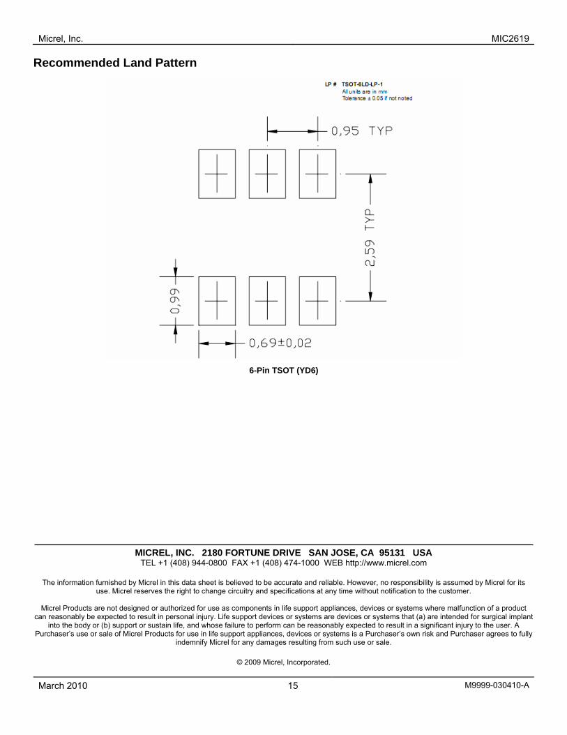
Recommended Land Pattern
6-Pin TSOT (YD6)
MICREL, INC. 2180 FORTUNE DRIVE SAN JOSE, CA 95131 USA TEL +1 (408) 944-0800 FAX +1 (408) 474-1000 WEB http://www.micrel.com
The information furnished by Micrel in this data sheet is believed to be accurate and reliable. However, no responsibility is assumed by Micrel for its
use. Micrel reserves the right to change circuitry and specifications at any time without notification to the customer.
Micrel Products are not designed or authorized for use as components in life support appliances, devices or systems where malfunction of a product can reasonably be expected to result in personal injury. Life support devices or systems are devices or systems that (a) are intended for surgical implant
into the body or (b) support or sustain life, and whose failure to perform can be reasonably expected to result in a significant injury to the user. A Purchaser’s use or sale of Micrel Products for use in life support appliances, devices or systems is a Purchaser’s own risk and Purchaser agrees to fully
indemnify Micrel for any damages resulting from such use or sale.
© 2009 Micrel, Incorporated.