microchip oscillators and clocks using ... -...
TRANSCRIPT

Microchip Oscillators and Clocks Using
Microelectromechanical Systems (MEMS) Technology
OVERVIEW
For decades, oscillators and clocks have relied onquartz crystals for the creation of a stable frequencyreference. Crystals perform very well for many applica-tions. However, microelectromechanical systems(MEMS) technology, replacing quartz crystals withMEMS resonators, entered the marketplace ten yearsago and is rapidly maturing.
MEMS-based timing devices offer high reliability(including AEC-Q100 certification for automotive use),extended operating temperatures, small size, and lowpower consumption. Video surveillance, automotiveADAS, general industrial applications, and data trans-mission to 10 Gbps are prime areas of usage today.
The next milestone will be next-generation MEMS res-onators that achieve very low phase noise for high-endcommunication systems.
Microchip acquired MEMS timing technology throughthe purchases of Discera and Micrel in 2015. Since Dis-cera shipped its first production oscillators in 2008,almost 100 million devices have been manufacturedand sold.
This paper describes the benefits of a MEMS-basedsolution, the resonator technology, and the design ofthe final product.
KEY FUNCTIONALITY
Microchip’s MEMS-based oscillators and clocks offerbenefits over traditional quartz solutions (Figure 1).These include stable frequency, small size, high reli-ability, flexibility, many programmable features, fastguaranteed start-up, and high integration.
FIGURE 1: Benefits of Microchip MEMS-Based Oscillators and Clocks.
Author: John Clark and Graham MostynMicrochip Technology Inc.
2017 Microchip Technology Inc. DS00002344A-page 1
MICROCHIP RESONATOR TECHNOLOGY
The FFS Resonator
Microchip’s MEMS resonator products evolved out ofresearch at the University of Michigan. That work wassome of the earliest to take existing MEMS resonatortechnology and begin to mold it to fit real wireless andtiming applications. The Microchip resonator design isreferred to as the FFS resonator, or Free-Free beamShort support resonator, which was an iteration on theFree-Free Beam resonator pioneered at U of M. TheFFS design, shown in Figure 2, uses short anchor sup-ports to make the design more rigid, and consists of awide resonator beam to improve its power handling—acritical feature for oscillator design. The beam contactsthe substrate at only the four anchor locations and sitsabove it, separated by a narrow gap that leaves the res-onator free to move. The FFS resonator itself isextremely compact compared to quartz crystals, mea-suring only 50 µm x 30 µm for an 18 MHz device.
FIGURE 2: SEM of a Production FFS Resonator Beam.
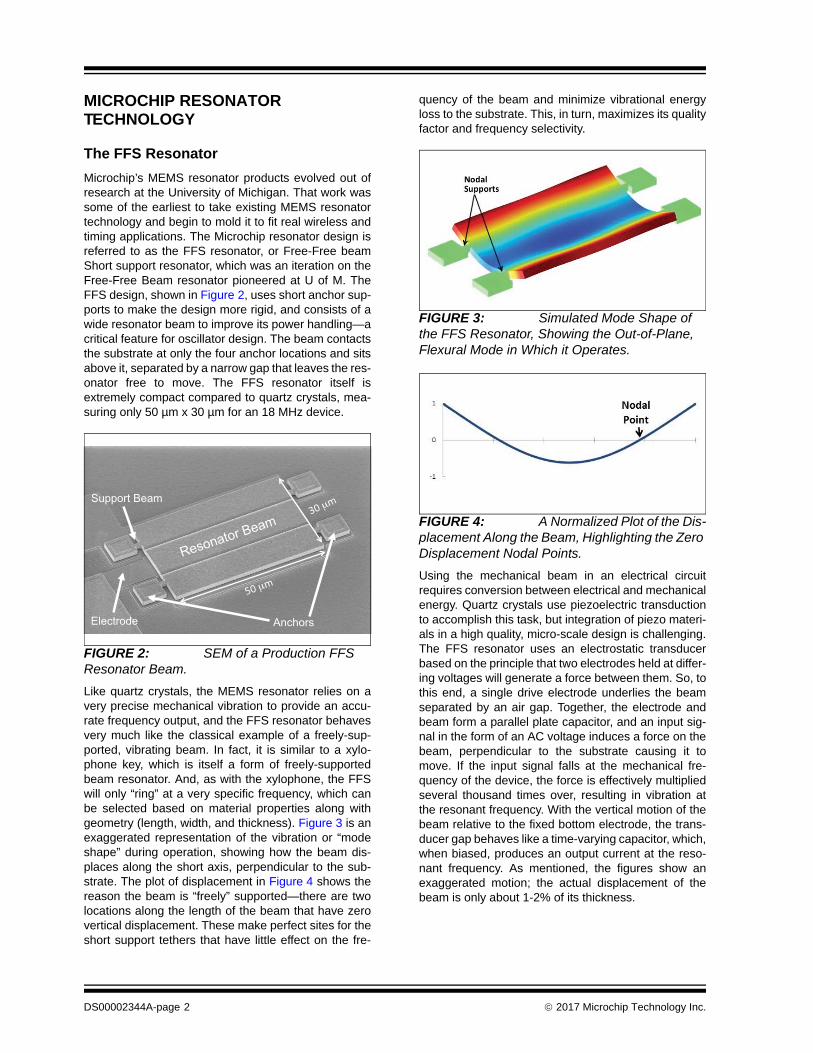
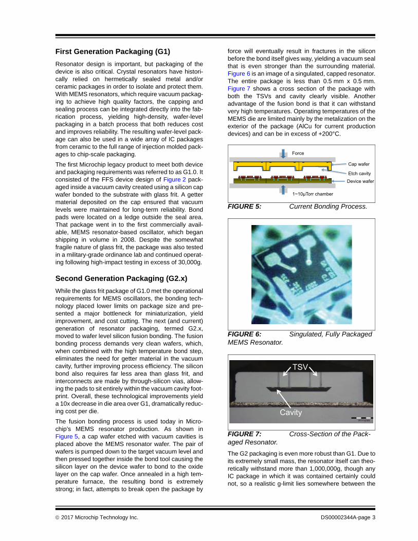
Like quartz crystals, the MEMS resonator relies on avery precise mechanical vibration to provide an accu-rate frequency output, and the FFS resonator behavesvery much like the classical example of a freely-sup-ported, vibrating beam. In fact, it is similar to a xylo-phone key, which is itself a form of freely-supportedbeam resonator. And, as with the xylophone, the FFSwill only “ring” at a very specific frequency, which canbe selected based on material properties along withgeometry (length, width, and thickness). Figure 3 is anexaggerated representation of the vibration or “modeshape” during operation, showing how the beam dis-places along the short axis, perpendicular to the sub-strate. The plot of displacement in Figure 4 shows thereason the beam is “freely” supported—there are twolocations along the length of the beam that have zerovertical displacement. These make perfect sites for theshort support tethers that have little effect on the fre-
quency of the beam and minimize vibrational energyloss to the substrate. This, in turn, maximizes its qualityfactor and frequency selectivity.
FIGURE 3: Simulated Mode Shape of the FFS Resonator, Showing the Out-of-Plane, Flexural Mode in Which it Operates.
FIGURE 4: A Normalized Plot of the Dis-placement Along the Beam, Highlighting the Zero Displacement Nodal Points.
Using the mechanical beam in an electrical circuitrequires conversion between electrical and mechanicalenergy. Quartz crystals use piezoelectric transductionto accomplish this task, but integration of piezo materi-als in a high quality, micro-scale design is challenging.The FFS resonator uses an electrostatic transducerbased on the principle that two electrodes held at differ-ing voltages will generate a force between them. So, tothis end, a single drive electrode underlies the beamseparated by an air gap. Together, the electrode andbeam form a parallel plate capacitor, and an input sig-nal in the form of an AC voltage induces a force on thebeam, perpendicular to the substrate causing it tomove. If the input signal falls at the mechanical fre-quency of the device, the force is effectively multipliedseveral thousand times over, resulting in vibration atthe resonant frequency. With the vertical motion of thebeam relative to the fixed bottom electrode, the trans-ducer gap behaves like a time-varying capacitor, which,when biased, produces an output current at the reso-nant frequency. As mentioned, the figures show anexaggerated motion; the actual displacement of thebeam is only about 1-2% of its thickness.
!"#$%&'$()
*"&+)
,-..$(')*"&+)
/%01$(#)
Resonator Beam
Support Beam
Electrode Anchors
DS00002344A-page 2 2017 Microchip Technology Inc.
First Generation Packaging (G1)
Resonator design is important, but packaging of thedevice is also critical. Crystal resonators have histori-cally relied on hermetically sealed metal and/orceramic packages in order to isolate and protect them.With MEMS resonators, which require vacuum packag-ing to achieve high quality factors, the capping andsealing process can be integrated directly into the fab-rication process, yielding high-density, wafer-levelpackaging in a batch process that both reduces costand improves reliability. The resulting wafer-level pack-age can also be used in a wide array of IC packagesfrom ceramic to the full range of injection molded pack-ages to chip-scale packaging.
The first Microchip legacy product to meet both deviceand packaging requirements was referred to as G1.0. Itconsisted of the FFS device design of Figure 2 pack-aged inside a vacuum cavity created using a silicon capwafer bonded to the substrate with glass frit. A gettermaterial deposited on the cap ensured that vacuumlevels were maintained for long-term reliability. Bondpads were located on a ledge outside the seal area.That package went in to the first commercially avail-able, MEMS resonator-based oscillator, which beganshipping in volume in 2008. Despite the somewhatfragile nature of glass frit, the package was also testedin a military-grade ordinance lab and continued operat-ing following high-impact testing in excess of 30,000g.
Second Generation Packaging (G2.x)
While the glass frit package of G1.0 met the operationalrequirements for MEMS oscillators, the bonding tech-nology placed lower limits on package size and pre-sented a major bottleneck for miniaturization, yieldimprovement, and cost cutting. The next (and current)generation of resonator packaging, termed G2.x,moved to wafer level silicon fusion bonding. The fusionbonding process demands very clean wafers, which,when combined with the high temperature bond step,eliminates the need for getter material in the vacuumcavity, further improving process efficiency. The siliconbond also requires far less area than glass frit, andinterconnects are made by through-silicon vias, allow-ing the pads to sit entirely within the vacuum cavity foot-print. Overall, these technological improvements yielda 10x decrease in die area over G1, dramatically reduc-ing cost per die.
The fusion bonding process is used today in Micro-chip’s MEMS resonator production. As shown inFigure 5, a cap wafer etched with vacuum cavities isplaced above the MEMS resonator wafer. The pair ofwafers is pumped down to the target vacuum level andthen pressed together inside the bond tool causing thesilicon layer on the device wafer to bond to the oxidelayer on the cap wafer. Once annealed in a high tem-perature furnace, the resulting bond is extremelystrong; in fact, attempts to break open the package by
force will eventually result in fractures in the siliconbefore the bond itself gives way, yielding a vacuum sealthat is even stronger than the surrounding material.Figure 6 is an image of a singulated, capped resonator.The entire package is less than 0.5 mm x 0.5 mm.Figure 7 shows a cross section of the package withboth the TSVs and cavity clearly visible. Anotheradvantage of the fusion bond is that it can withstandvery high temperatures. Operating temperatures of theMEMS die are limited mainly by the metalization on theexterior of the package (AlCu for current productiondevices) and can be in excess of +200°C.
FIGURE 5: Current Bonding Process.
FIGURE 6: Singulated, Fully Packaged MEMS Resonator.
FIGURE 7: Cross-Section of the Pack-aged Resonator.
The G2 packaging is even more robust than G1. Due toits extremely small mass, the resonator itself can theo-retically withstand more than 1,000,000g, though anyIC package in which it was contained certainly couldnot, so a realistic g-limit lies somewhere between the
Cap wafer
Device wafer
Etch cavity
Force
1~10μTorr chamber
TSV
Cavity
2017 Microchip Technology Inc. DS00002344A-page 3

G1 package at 30,000g and that upper bound, severalorders of magnitude beyond what a typical crystal canwithstand at around 50g–100g.
Long-term stability, or aging, is also a critical metric foran oscillator. Figure 8 shows a plot of the resonant fre-quency of eight MEMS devices aged under constantoperation at +85°C for 1,000 hours. Average drift isroughly –1.5 ppm over the course of the test (straightline regions in the plot indicate data collection errors;the parts remained powered and at temperaturethroughout). Figure 9 shows a plot of the calibrated out-put frequency from 16 different Microchip DSC60xxoscillators under the same conditions. Aging mecha-nisms in the ASIC cause some spread in the results,but can be limited by careful design. The oscillatorshows an average shift of roughly 1 ppm over thecourse of the aging, closely following the behavior ofthe MEMS.
FIGURE 8: Plots of Device Aging at +85°C for 1,000 hours.
FIGURE 9: Aging of the DSC60xx.
Third Generation Resonators (G3 and Beyond)
All products in current production (as of December,2016) use the G2.x resonators. They provide excellentperformance for many XO applications.
A number of design refinements can lead to improvedperformance for applications that require ultra-low jitter.The G3 resonator, pictured in Figure 10, was designedin order to meet these more demanding applicationsand to provide reduced jitter and spurs along with thepotential for even better temperature stability. The G3design is a 15th overtone FFS beam resonator operat-ing at approximately 70 MHz. Similar to higher fre-quency crystals, the resonator utilizes a higher ordermode to achieve higher frequency and better perfor-mance. In the 15th overtone mode shape, shown insimulation in Figure 11 and simplified form in Figure 12,there are 16 inflection points and 17 nodal points, com-pared to 1 inflection and 2 nodal points for the G2 fun-damental mode design. The result is a much largerresonator with increased transducer area that, whencombined with higher stiffness at higher frequency, dra-matically increases power handling in-turn improvingphase noise and jitter. The higher operating frequencyalso improves phase noise by reducing the multiplierused in the PLL to up-convert to the VCO frequency.
The G3 resonator was also designed to operate in a dif-ferential mode. As shown schematically in Figure 12,electrodes under each inflection point can be groupedtogether into full, 4-port differential operation. Thisgreatly reduces any common mode noise and interfer-ence that could contribute to overall jitter.
While the G3 design offers a path to improved clockpurity, other design improvements also lead toimproved temperature stability. Overall temperatureperformance is a complex interaction of factors includ-ing temperature sensor accuracy, sensor offsets fromactual MEMS temperature, and temperature sensitivityof the MEMS resonator itself. Polysilicon FFS resona-tors have an inherent temperature coefficient of fre-quency or TCf of about –17 ppm/°C due largely to thedecrease in polysilicon stiffness as temperatureincreases. However, silicon dioxide increases in stiff-ness with temperature. In a composite resonator struc-ture with alternating layers of polysilicon and oxide, thechanges in stiffness can be designed to cancel out,effectively reducing the TCf by an order of magnitudeor more. This method has been applied to both G2 andG3 designs and has been shown to dramaticallyimprove frequency stability across temperature.
FIGURE 10: SEM of the G3 Resonator.
L r = 170μm
DS00002344A-page 4 2017 Microchip Technology Inc.
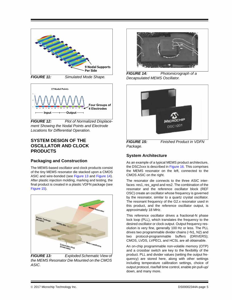
FIGURE 11: Simulated Mode Shape.
FIGURE 12: Plot of Normalized Displace-ment Showing the Nodal Points and Electrode Locations for Differential Operation.
SYSTEM DESIGN OF THE OSCILLATOR AND CLOCK PRODUCTS
Packaging and Construction
The MEMS-based oscillator and clock products consistof the tiny MEMS resonator die stacked upon a CMOSASIC and wire-bonded (see Figure 13 and Figure 14).After plastic injection molding, marking and testing, thefinal product is created in a plastic VDFN package (seeFigure 15).
FIGURE 13: Exploded Schematic View of the MEMS Resonator Die Mounted on the CMOS ASIC.
FIGURE 14: Photomicrograph of a Decapsulated MEMS Oscillator.
FIGURE 15: Finished Product in VDFN Package.
System Architecture
As an example of a typical MEMS product architecture,the DSC2xxx is described in Figure 16. This comprisesthe MEMS resonator on the left, connected to theCMOS ASIC on the right.
The resonator die connects to the three ASIC inter-faces: res1, res_agnd and res2. The combination of theresonator and the reference oscillator block (REFOSC) create an oscillator whose frequency is governedby the resonator, similar to a quartz crystal oscillator.The resonant frequency of the G2.x resonator used inthis product, and the reference oscillator output, isapproximately 18 MHz.
This reference oscillator drives a fractional-N phaselock loop (PLL), which translates the frequency to thedesired oscillator or clock output. Output frequency res-olution is very fine, generally 100 Hz or less. The PLLdrives two programmable divider chains (÷N1, N2) andtwo protocol-programmable buffers (DRIVERS);CMOS, LVDS, LVPECL and HCSL are all obtainable.
An on-chip programmable non-volatile memory (OTP)and a crossbar switch are key to the flexibility of theproduct. PLL and divider values (setting the output fre-quency) are stored here, along with other settingsincluding temperature calibration settings, choice ofoutput protocol, rise/fall time control, enable pin pull-up/down, and many more.
Four Groups of4 Electrodes
Input Output+ – + – + – + – + – + – + – + –
2017 Microchip Technology Inc. DS00002344A-page 5

FIGURE 16: DSC2xxx Product Block Diagram.
Frequency Stability Over Temperature
The temperature sensor (TEMP SENSOR) produces adigital representation of the die temperature, and this ispassed to the fractional-N phase lock loop to correct fornatural spreads in the absolute frequency of the reso-nator, as well as its temperature coefficient. The systemis calibrated in manufacturing, with adjustment coeffi-cients programmed into the ROM. The result is an out-put frequency that is programmable to 100 Hz or so,and extremely stable to ±10 ppm across extended tem-perature ranges (see Figure 17).
FIGURE 17: Frequency Stability of Micro-chip’s MEMS Oscillator Compared to Quartz Oscillators.
Output Clock Jitter
A MEMS resonator produces the lowest jitter if it isdriven at a maximum level; however, too high a drivelevel will produce unwanted frequency shifts. This max-
imum level varies with die temperature, and the tem-perature sensor analog output is used to optimize thedrive current of the oscillator at all temperatures.
Figure 18 shows the integrated phase jitter of theDSC1xxx and DSC2xxx families, ideal for many net-working applications. Different applications are sensi-tive to phase noise over different frequency ranges; thetiming industry generally uses 12 kHz to 20 MHz as abenchmark, dating back to SONET technology. How-ever, today’s high speed wired networks, using clock-data recovery locked loops, are tolerant to noise nearthe carrier (also called “close-in” or “low frequency off-set” noise), and are only sensitive to noise in certainbandwidths at higher carrier offset frequencies. TheDSC1xxx and DSC2xxx families achieve 450 fs in the200 kHz to 20 MHz band, suitable for 1 Gigabit Ether-net, and are also qualified for XAUI and PCIe.
MEMS oscillators in production today produce more“close-in” noise (noise at offset frequencies below5 kHz) than non-PLL fixed-frequency quartz oscillators.This is because the very small resonator produces alow amplitude reference signal closer to the noise floor.At high offset frequencies, this noise is filtered out bythe PLL. However at low offset frequencies, it is passedto the output. As explained above, this is a non-issuefor most applications, as they are only sensitive tonoise above about 100 kHz.
The new G3 generation of MEMS resonators can bedriven with more energy and produce even lowerphase noise, comparable with fixed-frequency quartzcrystal oscillators in the 12 kHz to 20 MHz bandwidth.
Microchip’s MEMS LVPECL 156.25MHzCompetitor 1Competitor 2Competitor 3
Freq
uenc
y D
evia
tion
(PP
M)
High Stability Over Extended TemperatureTemperature (°C)
–50 –40 –30 –20 –10 0 10 20 30 40 50 60 70 80 90 100 110 120 130 140
60
50
40
30
20
10
0
–10
–20
DS00002344A-page 6 2017 Microchip Technology Inc.
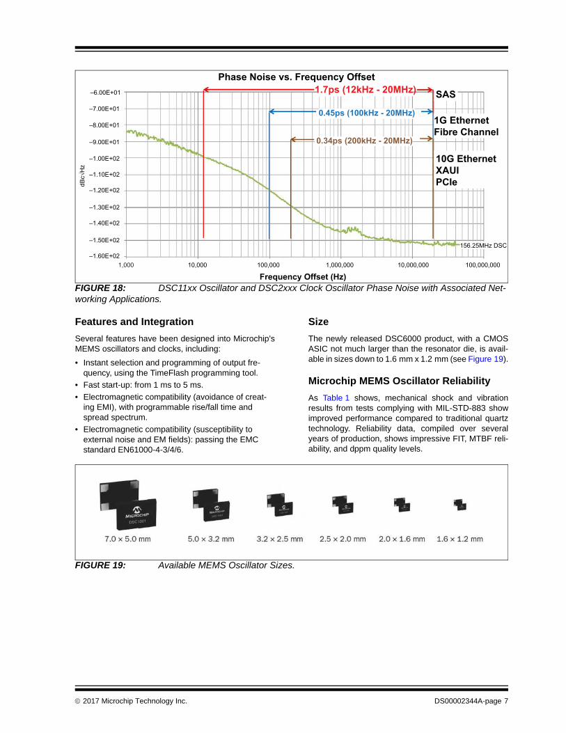
FIGURE 18: DSC11xx Oscillator and DSC2xxx Clock Oscillator Phase Noise with Associated Net-working Applications.
Features and Integration
Several features have been designed into Microchip’sMEMS oscillators and clocks, including:
• Instant selection and programming of output fre-quency, using the TimeFlash programming tool.
• Fast start-up: from 1 ms to 5 ms.
• Electromagnetic compatibility (avoidance of creat-ing EMI), with programmable rise/fall time and spread spectrum.
• Electromagnetic compatibility (susceptibility to external noise and EM fields): passing the EMC standard EN61000-4-3/4/6.
Size
The newly released DSC6000 product, with a CMOSASIC not much larger than the resonator die, is avail-able in sizes down to 1.6 mm x 1.2 mm (see Figure 19).
Microchip MEMS Oscillator Reliability
As Table 1 shows, mechanical shock and vibrationresults from tests complying with MIL-STD-883 showimproved performance compared to traditional quartztechnology. Reliability data, compiled over severalyears of production, shows impressive FIT, MTBF reli-ability, and dppm quality levels.
FIGURE 19: Available MEMS Oscillator Sizes.
156.25MHz DSC
1,000 10,000
Frequency Offset (Hz)100,000 1,000,000 10,000,000 100,000,000
–6.00E+01
–7.00E+01
–8.00E+01
–9.00E+01
–1.00E+02
–1.10E+02
–1.20E+02
–1.30E+02
–1.40E+02
–1.50E+02
–1.60E+02
Phase Noise vs. Frequency Offset1.7ps (12kHz - 20MHz) SAS
0.45ps (100kHz - 20MHz)1G EthernetFibre Channel
0.34ps (200kHz - 20MHz)
10G EthernetXAUIPCIe
2017 Microchip Technology Inc. DS00002344A-page 7
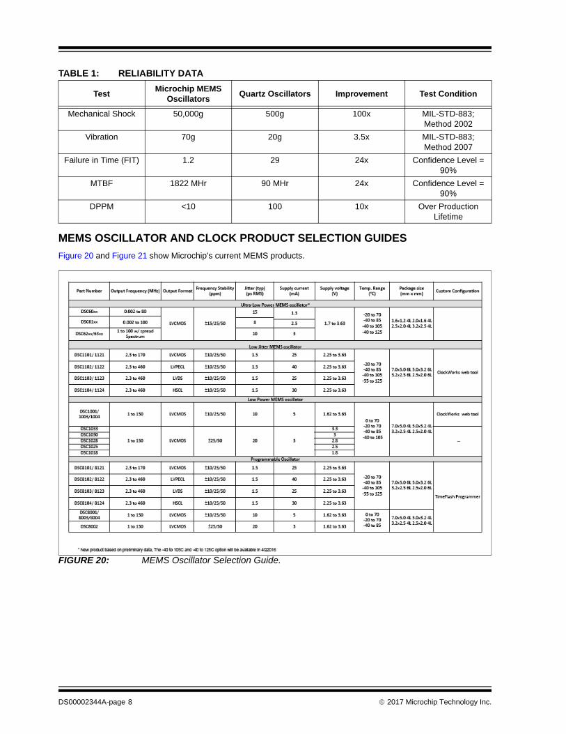
MEMS OSCILLATOR AND CLOCK PRODUCT SELECTION GUIDES
Figure 20 and Figure 21 show Microchip’s current MEMS products.
FIGURE 20: MEMS Oscillator Selection Guide.
TABLE 1: RELIABILITY DATA
TestMicrochip MEMS
OscillatorsQuartz Oscillators Improvement Test Condition
Mechanical Shock 50,000g 500g 100x MIL-STD-883; Method 2002
Vibration 70g 20g 3.5x MIL-STD-883; Method 2007
Failure in Time (FIT) 1.2 29 24x Confidence Level = 90%
MTBF 1822 MHr 90 MHr 24x Confidence Level = 90%
DPPM <10 100 10x Over Production Lifetime
DS00002344A-page 8 2017 Microchip Technology Inc.
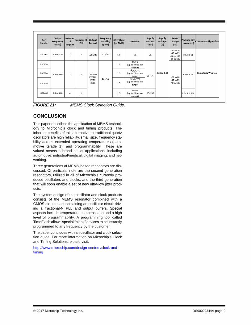
FIGURE 21: MEMS Clock Selection Guide.
CONCLUSION
This paper described the application of MEMS technol-ogy to Microchip’s clock and timing products. Theinherent benefits of this alternative to traditional quartzoscillators are high reliability, small size, frequency sta-bility across extended operating temperatures (auto-motive Grade 1), and programmability. These arevalued across a broad set of applications, includingautomotive, industrial/medical, digital imaging, and net-working.
Three generations of MEMS-based resonators are dis-cussed. Of particular note are the second generationresonators, utilized in all of Microchip’s currently pro-duced oscillators and clocks, and the third generationthat will soon enable a set of new ultra-low jitter prod-ucts.
The system design of the oscillator and clock productsconsists of the MEMS resonator combined with aCMOS die, the last containing an oscillator circuit driv-ing a fractional-N PLL and output buffers. Specialaspects include temperature compensation and a highlevel of programmability. A programming tool calledTimeFlash allows special “blank” devices to be instantlyprogrammed to any frequency by the customer.
The paper concludes with an oscillator and clock selec-tion guide. For more information on Microchip’s Clockand Timing Solutions, please visit:
http://www.microchip.com/design-centers/clock-and-timing
2017 Microchip Technology Inc. DS00002344A-page 9
NOTES:
DS00002344A-page 10 2017 Microchip Technology Inc.
Note the following details of the code protection feature on Microchip devices:
• Microchip products meet the specification contained in their particular Microchip Data Sheet.
• Microchip believes that its family of products is one of the most secure families of its kind on the market today, when used in the intended manner and under normal conditions.
• There are dishonest and possibly illegal methods used to breach the code protection feature. All of these methods, to our knowledge, require using the Microchip products in a manner outside the operating specifications contained in Microchip’s Data Sheets. Most likely, the person doing so is engaged in theft of intellectual property.
• Microchip is willing to work with the customer who is concerned about the integrity of their code.
• Neither Microchip nor any other semiconductor manufacturer can guarantee the security of their code. Code protection does not mean that we are guaranteeing the product as “unbreakable.”
Code protection is constantly evolving. We at Microchip are committed to continuously improving the code protection features of ourproducts. Attempts to break Microchip’s code protection feature may be a violation of the Digital Millennium Copyright Act. If such actsallow unauthorized access to your software or other copyrighted work, you may have a right to sue for relief under that Act.
Information contained in this publication regarding deviceapplications and the like is provided only for your convenienceand may be superseded by updates. It is your responsibility toensure that your application meets with your specifications.MICROCHIP MAKES NO REPRESENTATIONS ORWARRANTIES OF ANY KIND WHETHER EXPRESS ORIMPLIED, WRITTEN OR ORAL, STATUTORY OROTHERWISE, RELATED TO THE INFORMATION,INCLUDING BUT NOT LIMITED TO ITS CONDITION,QUALITY, PERFORMANCE, MERCHANTABILITY ORFITNESS FOR PURPOSE. Microchip disclaims all liabilityarising from this information and its use. Use of Microchipdevices in life support and/or safety applications is entirely atthe buyer’s risk, and the buyer agrees to defend, indemnify andhold harmless Microchip from any and all damages, claims,suits, or expenses resulting from such use. No licenses areconveyed, implicitly or otherwise, under any Microchipintellectual property rights unless otherwise stated.
2017 Microchip Technology Inc.
Microchip received ISO/TS-16949:2009 certification for its worldwide headquarters, design and wafer fabrication facilities in Chandler and Tempe, Arizona; Gresham, Oregon and design centers in California and India. The Company’s quality system processes and procedures are for its PIC® MCUs and dsPIC® DSCs, KEELOQ® code hopping devices, Serial EEPROMs, microperipherals, nonvolatile memory and analog products. In addition, Microchip’s quality system for the design and manufacture of development systems is ISO 9001:2000 certified.
QUALITYMANAGEMENTSYSTEMCERTIFIEDBYDNV
== ISO/TS16949==
Trademarks
The Microchip name and logo, the Microchip logo, AnyRate, AVR, AVR logo, AVR Freaks, BeaconThings, BitCloud, CryptoMemory, CryptoRF, dsPIC, FlashFlex, flexPWR, Heldo, JukeBlox, KEELOQ, KEELOQ logo, Kleer, LANCheck, LINK MD, maXStylus, maXTouch, MediaLB, megaAVR, MOST, MOST logo, MPLAB, OptoLyzer, PIC, picoPower, PICSTART, PIC32 logo, Prochip Designer, QTouch, RightTouch, SAM-BA, SpyNIC, SST, SST Logo, SuperFlash, tinyAVR, UNI/O, and XMEGA are registered trademarks of Microchip Technology Incorporated in the U.S.A. and other countries.
ClockWorks, The Embedded Control Solutions Company, EtherSynch, Hyper Speed Control, HyperLight Load, IntelliMOS, mTouch, Precision Edge, and Quiet-Wire are registered trademarks of Microchip Technology Incorporated in the U.S.A.
Adjacent Key Suppression, AKS, Analog-for-the-Digital Age, Any Capacitor, AnyIn, AnyOut, BodyCom, chipKIT, chipKIT logo, CodeGuard, CryptoAuthentication, CryptoCompanion, CryptoController, dsPICDEM, dsPICDEM.net, Dynamic Average Matching, DAM, ECAN, EtherGREEN, In-Circuit Serial Programming, ICSP, Inter-Chip Connectivity, JitterBlocker, KleerNet, KleerNet logo, Mindi, MiWi, motorBench, MPASM, MPF, MPLAB Certified logo, MPLIB, MPLINK, MultiTRAK, NetDetach, Omniscient Code Generation, PICDEM, PICDEM.net, PICkit, PICtail, PureSilicon, QMatrix, RightTouch logo, REAL ICE, Ripple Blocker, SAM-ICE, Serial Quad I/O, SMART-I.S., SQI, SuperSwitcher, SuperSwitcher II, Total Endurance, TSHARC, USBCheck, VariSense, ViewSpan, WiperLock, Wireless DNA, and ZENA are trademarks of Microchip Technology Incorporated in the U.S.A. and other countries.
SQTP is a service mark of Microchip Technology Incorporated in the U.S.A.
Silicon Storage Technology is a registered trademark of Microchip Technology Inc. in other countries.
GestIC is a registered trademark of Microchip Technology Germany II GmbH & Co. KG, a subsidiary of Microchip Technology Inc., in other countries.
All other trademarks mentioned herein are property of their respective companies.
© 2017, Microchip Technology Incorporated, All Rights Reserved.
ISBN: 978-1-5224-1360-8
DS00002344A-page 11
DS00002344A-page 12 2017 Microchip Technology Inc.
AMERICASCorporate Office2355 West Chandler Blvd.Chandler, AZ 85224-6199Tel: 480-792-7200 Fax: 480-792-7277Technical Support: http://www.microchip.com/supportWeb Address: www.microchip.com
AtlantaDuluth, GA Tel: 678-957-9614 Fax: 678-957-1455
Austin, TXTel: 512-257-3370
BostonWestborough, MA Tel: 774-760-0087 Fax: 774-760-0088
ChicagoItasca, IL Tel: 630-285-0071 Fax: 630-285-0075
DallasAddison, TX Tel: 972-818-7423 Fax: 972-818-2924
DetroitNovi, MI Tel: 248-848-4000
Houston, TX Tel: 281-894-5983
IndianapolisNoblesville, IN Tel: 317-773-8323Fax: 317-773-5453Tel: 317-536-2380
Los AngelesMission Viejo, CA Tel: 949-462-9523Fax: 949-462-9608Tel: 951-273-7800
Raleigh, NC Tel: 919-844-7510
New York, NY Tel: 631-435-6000
San Jose, CA Tel: 408-735-9110Tel: 408-436-4270
Canada - TorontoTel: 905-695-1980 Fax: 905-695-2078
ASIA/PACIFICAsia Pacific OfficeSuites 3707-14, 37th FloorTower 6, The GatewayHarbour City, Kowloon
Hong KongTel: 852-2943-5100Fax: 852-2401-3431
Australia - SydneyTel: 61-2-9868-6733Fax: 61-2-9868-6755
China - BeijingTel: 86-10-8569-7000 Fax: 86-10-8528-2104
China - ChengduTel: 86-28-8665-5511Fax: 86-28-8665-7889
China - ChongqingTel: 86-23-8980-9588Fax: 86-23-8980-9500
China - DongguanTel: 86-769-8702-9880
China - GuangzhouTel: 86-20-8755-8029
China - HangzhouTel: 86-571-8792-8115 Fax: 86-571-8792-8116
China - Hong Kong SARTel: 852-2943-5100 Fax: 852-2401-3431
China - NanjingTel: 86-25-8473-2460Fax: 86-25-8473-2470
China - QingdaoTel: 86-532-8502-7355Fax: 86-532-8502-7205
China - ShanghaiTel: 86-21-3326-8000 Fax: 86-21-3326-8021
China - ShenyangTel: 86-24-2334-2829Fax: 86-24-2334-2393
China - ShenzhenTel: 86-755-8864-2200 Fax: 86-755-8203-1760
China - WuhanTel: 86-27-5980-5300Fax: 86-27-5980-5118
China - XianTel: 86-29-8833-7252Fax: 86-29-8833-7256
ASIA/PACIFICChina - XiamenTel: 86-592-2388138 Fax: 86-592-2388130
China - ZhuhaiTel: 86-756-3210040 Fax: 86-756-3210049
India - BangaloreTel: 91-80-3090-4444 Fax: 91-80-3090-4123
India - New DelhiTel: 91-11-4160-8631Fax: 91-11-4160-8632
India - PuneTel: 91-20-3019-1500
Japan - OsakaTel: 81-6-6152-7160 Fax: 81-6-6152-9310
Japan - TokyoTel: 81-3-6880- 3770 Fax: 81-3-6880-3771
Korea - DaeguTel: 82-53-744-4301Fax: 82-53-744-4302
Korea - SeoulTel: 82-2-554-7200Fax: 82-2-558-5932 or 82-2-558-5934
Malaysia - Kuala LumpurTel: 60-3-6201-9857Fax: 60-3-6201-9859
Malaysia - PenangTel: 60-4-227-8870Fax: 60-4-227-4068
Philippines - ManilaTel: 63-2-634-9065Fax: 63-2-634-9069
SingaporeTel: 65-6334-8870Fax: 65-6334-8850
Taiwan - Hsin ChuTel: 886-3-5778-366Fax: 886-3-5770-955
Taiwan - KaohsiungTel: 886-7-213-7830
Taiwan - TaipeiTel: 886-2-2508-8600 Fax: 886-2-2508-0102
Thailand - BangkokTel: 66-2-694-1351Fax: 66-2-694-1350
EUROPEAustria - WelsTel: 43-7242-2244-39Fax: 43-7242-2244-393
Denmark - CopenhagenTel: 45-4450-2828 Fax: 45-4485-2829
Finland - EspooTel: 358-9-4520-820
France - ParisTel: 33-1-69-53-63-20 Fax: 33-1-69-30-90-79
France - Saint CloudTel: 33-1-30-60-70-00
Germany - GarchingTel: 49-8931-9700Germany - HaanTel: 49-2129-3766400
Germany - HeilbronnTel: 49-7131-67-3636
Germany - KarlsruheTel: 49-721-625370
Germany - MunichTel: 49-89-627-144-0 Fax: 49-89-627-144-44
Germany - RosenheimTel: 49-8031-354-560
Israel - Ra’anana Tel: 972-9-744-7705
Italy - Milan Tel: 39-0331-742611 Fax: 39-0331-466781
Italy - PadovaTel: 39-049-7625286
Netherlands - DrunenTel: 31-416-690399 Fax: 31-416-690340
Norway - TrondheimTel: 47-7289-7561
Poland - WarsawTel: 48-22-3325737
Romania - BucharestTel: 40-21-407-87-50
Spain - MadridTel: 34-91-708-08-90Fax: 34-91-708-08-91
Sweden - GothenbergTel: 46-31-704-60-40
Sweden - StockholmTel: 46-8-5090-4654
UK - WokinghamTel: 44-118-921-5800Fax: 44-118-921-5820
Worldwide Sales and Service
11/07/16