microcontroller (1) lab manual - fadhl alakwaa, phd...
TRANSCRIPT
UNIVERSITY OF SCIENCE ampTECHNOLEGYFACUALTY OF ENGNEERINGBIOMEDICAL
Microcontroller (1) Lab Manual
Part (3)
Prepared By
Eng Mohsen Ali AL-awamiSupervise red By
Dr Fadel AL-aqawa2010-2011
1
UNIVERSITY OF SCIENCE ampTECHNOLEGYFACUALTY OF ENGNEERINGBIOMEDICAL
LAB Expeirment (3)
Main Topics Switch Debouncing (port as IO PROGRAMMER) TIMER Counter PROGRAMMING
Learning ObjectivesTasks
Upon Compliation this expeirment you will be able to
Using the port pins as input throught the switchs List the timers mode of the 8051 and their associated
registers Describe the various modes of the 8051 timers Programs the 8051 timers to generate time delays Programs the 8051 counters as event counters
2
UNIVERSITY OF SCIENCE ampTECHNOLEGYFACUALTY OF ENGNEERINGBIOMEDICAL
Switch Debouncing (port as IO PROGRAMMER)
There are times that we need to access only 1 or 2 bits of the port instead of 8 bites a powerful features of the 8051 IO ports is their capability to access individual bits of the port without altering the rest of the bits in the port
Example 1
The following code toggles the bit p12 continuously
3
Back CPL P12 complement p12 only
ACALL DELAY
SJMP BACK
another variation of the above program follows
AGAIN SETB P12 change only p12=high
ACALL DELAY
CLR P12 change only p12=low
ACALL DELAY
SJMP AGAIN
UNIVERSITY OF SCIENCE ampTECHNOLEGYFACUALTY OF ENGNEERINGBIOMEDICAL
Example 2
4
Write a program to perform the following
(a) Keep mentoring the p12 bit until it become high (b) When p12 becomes high write value 45h to port 0 (c) Send a high ndashto- low pulse to p23
Solution
SETB P12 make switch p12 an input switch
MOV A 45H A=45h
AGAIN JNB P12 AGAIN get out when p12 =1
Mov P0A mov A to P0
SETB P23 make P23 high
CLR P23 make p23 low for H-TO-L
In this program instruction (JNB P12 AGAIN ) stays in the loop as long as p12 is low When p12 becomes high it gets out of the loop and write the value of 45H in to port 0 and creat H--TO ndashL pluse by the sequence of the instructions SETB and CLR
UNIVERSITY OF SCIENCE ampTECHNOLEGYFACUALTY OF ENGNEERINGBIOMEDICAL
PROGRAMMING TIMERS
The 8051 has two timers they can be used either as Timers to generate a time delay or as Event counters to count events happening
outside the microcontroller Both Timer 0 and Timer 1 are 16 bitswide
Since 8051 has an 8-bit architecture each 16-bits timer is accessed as two separate registers of low byte and high byte
Timer 0 amp 1 Registers
Accessed as low byte and high byte The low byte register is called TL0TL1
And The high byte register is called TH0TH1 Accessed like any other register MOV TL04FH MOV R5TH0
D15
D14
D13
D12
D11
D10
D9
D8
D7
D6
D5
D4
D3
D2
D1
D0
------------------------------------------- ------------------------------ TH0 TL0
5
UNIVERSITY OF SCIENCE ampTECHNOLEGYFACUALTY OF ENGNEERINGBIOMEDICAL
D15
D14
D13
D12
D11
D10
D9
D8
D7
D6
D5
D4
D3
D2
D1
D0
------------------------------------------- ------------------------------ TH1 TL1
TMOD Register
Both timers 0 and 1 use the same register called TMOD (timer mode)set the various timer operation modes
TMOD is a 8-bit register The lower 4 bits are for Timer 0 The upper 4 bits are for Timer 1 In each case The lower 2 bits are used to set the timer mode The upper 2 bits to specify the operation
GATE CT M1 M0TIMER1
M1 M0 MODE OPERATING MODE0 0 0
13-bit timer mode 8-bit timercounter THx with TLx as 5-bit prescaler
0 1 1 16-bit timer mode 16-bit timercounter THx and TLx are cascaded there is no prescaler
6
GATE CT M1 M0TIMER0
UNIVERSITY OF SCIENCE ampTECHNOLEGYFACUALTY OF ENGNEERINGBIOMEDICAL
1 0 2 8-bit auto reload 8-bit auto reload timercounter THx
holds a value which is to be reloaded TLx each timeit overflows
1 1 3 Split timer mode
GATE Gating control when set Timercounter is enable only while the INTx pin is high and the TRx control pin is set When cleared the timer is enabled whenever the TRx control bit is set
CT Timer or counter selected Cleared for timer operation (input from internal system clock)Set for counter operation (input from Tx input pin)
7
Example 3Indicate which mode and which timer are selected for each of the following(a) MOV TMOD 01H (b) MOV TMOD 20H (c) MOV TMOD 12HSolutionWe convert the value from hex to binary From Figure 9-3 we have(a) TMOD = 00000001 mode 1 of timer 0 is selected(b) TMOD = 00100000 mode 2 of timer 1 is selected(c) TMOD = 00010010 mode 2 of timer 0 and mode 1 of timer 1 areselected
Example 4Find the timerrsquos clock frequency and its period for various 8051-based systemwith the crystal frequency 110592 MHz when CT bit of TMOD is 0
UNIVERSITY OF SCIENCE ampTECHNOLEGYFACUALTY OF ENGNEERINGBIOMEDICAL
Timers of 8051 do starting and stopping by either software or hardware control In using software to start and stop the timer where
GATE=0 1048707 The start and stop of the timer are controlled by
way of software by the TR (timer start) bits TR0 and TR1
1 The SETB instruction starts it and it is stopped by the CLR instruction
2 These instructions start and stop the timers as long as GATE=0 in the TMOD register
3 The hardware way of starting and stopping the timer by an external source is achieved by making GATE=1 in the TMOD register
Example 5
8
Solution112 times 110529 MHz = 9216 MHzT = 19216 kHz = 1085 us
XTAL
OSCILLATOR
12
Find the value for TMOD if we want to program timer 0 in mode 2use 8051 XTAL for the clock source and use instructions to start and stop the timerTMOD = 0000 0010
UNIVERSITY OF SCIENCE ampTECHNOLEGYFACUALTY OF ENGNEERINGBIOMEDICAL
Mode 1 Programming
The following are the characteristics and operations of mode11 It is a 16-bit timer therefore it allows value of 0000 to FFFFH to be loaded into the timerrsquos register TL and TH2 After TH and TL are loaded with a 16-bitinitial value the timer must be started This is done by SETB TR0 for timer 0 and SETB TR1 for timer 13 After the timer is started it starts to count up It counts up until it reaches its limit of FFFFH
TF goes high if Overfolw
CT =0 TR FFFF 0000 flag
3 When it rolls over from FFFFH to 0000 it sets high a flag bit called TF (timer flag)ndash Each timer has its own timer flag TF0 fortimer 0 and TF1 for timer 1ndash This timer flag can be monitored
9
XTAL
OSCILLATOR
12 TH TL TF
UNIVERSITY OF SCIENCE ampTECHNOLEGYFACUALTY OF ENGNEERINGBIOMEDICAL
1048707 When this timer flag is raised one option would be to stop the timer with the instructions CLR TR0 or CLR TR1 for timer 0 and timer 1 respectively4 After the timer reaches its limit and rolls over in order to repeat the process1048707 TH and TL must be reloaded with the original value and TF must be reloaded to 0To generate a time delay1 Load the TMOD value register indicating which timer (timer 0 or timer 1) is to be used and which timer mode (0 or 1) is selected2 Load registers TL and TH with initial count value3 Start the timer4 Keep monitoring the timer flag (TF) with the JNB TFxtarget instruction to see if it is raised1048707 Get out of the loop when TF becomes high5 Stop the timer6 Clear the TF flag for the next round7 Go back to Step 2 to load TH and TLAgain
10Example 6In the following program we create a square wave of 50 duty cycle (withequal portions high and low) on the P15 bit Timer 0 is used to generate the
UNIVERSITY OF SCIENCE ampTECHNOLEGYFACUALTY OF ENGNEERINGBIOMEDICAL
11
Example 6In the following program we create a square wave of 50 duty cycle (withequal portions high and low) on the P15 bit Timer 0 is used to generate the
Example 6 (contrsquo)DELAY SETB TR0 start the timer 0AGAIN JNB TF0AGAIN monitor timer flag 0 until it rolls over CLR TR0 stop timer 0 CLR TF0 clear timer 0 flag
UNIVERSITY OF SCIENCE ampTECHNOLEGYFACUALTY OF ENGNEERINGBIOMEDICAL
12
Example 6 (contrsquo)DELAY SETB TR0 start the timer 0AGAIN JNB TF0AGAIN monitor timer flag 0 until it rolls over CLR TR0 stop timer 0 CLR TF0 clear timer 0 flag
Example 7In Example 7 calculate the frequency of the square wave generatedon pin P15SolutionIn the timer delay calculation of Example 7 we did not include theoverhead due to instruction in the loop To get a more accurate timing
UNIVERSITY OF SCIENCE ampTECHNOLEGYFACUALTY OF ENGNEERINGBIOMEDICAL
13
Example 7In Example 7 calculate the frequency of the square wave generatedon pin P15SolutionIn the timer delay calculation of Example 7 we did not include theoverhead due to instruction in the loop To get a more accurate timing
Example 8Find the delay generated by timer 0 in the following code using bothof the Methods of Figure 9-4 Do not include the overhead due toinstruction CLR P23 Clear P23 MOV TMOD01 Timer 0 16-bitmode
UNIVERSITY OF SCIENCE ampTECHNOLEGYFACUALTY OF ENGNEERINGBIOMEDICAL
14
Example 8Find the delay generated by timer 0 in the following code using bothof the Methods of Figure 9-4 Do not include the overhead due toinstruction CLR P23 Clear P23 MOV TMOD01 Timer 0 16-bitmode
Example 8The following program generates a square wave on P15 continuouslyusing timer 1 for a time delay Find the frequency of the squarewave if XTAL = 110592 MHz In your calculation do not
UNIVERSITY OF SCIENCE ampTECHNOLEGYFACUALTY OF ENGNEERINGBIOMEDICAL
15
Example 8The following program generates a square wave on P15 continuouslyusing timer 1 for a time delay Find the frequency of the squarewave if XTAL = 110592 MHz In your calculation do not
UNIVERSITY OF SCIENCE ampTECHNOLEGYFACUALTY OF ENGNEERINGBIOMEDICAL
LAB Expeirment (4)
Main Topics LCD Pins DescriptionsLCD CommandsLCD Operations
Learning ObjectivesTasks
Upon Compliation this expeirment you will be able to
List reasons that LCD are gaging wide-spread usereplacing LEDrsquoS
Describe the function of the pins of atypical LCD List instruction command codes for programming an LCD Interface an LCD to the 8051 Program an LCD by sending data or commands to it from
8051
16
UNIVERSITY OF SCIENCE ampTECHNOLEGYFACUALTY OF ENGNEERINGBIOMEDICAL
INTERFACING LCD TO 8051
8051 LCD
5v
10k pot
LCD Operation
LCD is finding widespread use replacing LEDs1048707 The declining prices of LCD1048707 The ability to display numbers characters and graphics1048707 Incorporation of a refreshing controller into the LCD thereby relieving the CPU of the task of refreshing the LCD1048707 Ease of programming for characters and graphicsLCD PinDescriptions
17
P01
P07
P20
P21
P23
D0 Vcc
Vee
D7 Vss
RS RW E
UNIVERSITY OF SCIENCE ampTECHNOLEGYFACUALTY OF ENGNEERINGBIOMEDICAL
LCD Pin Descriptions
Pin Descriptions for LCD
pin symbol
IO Descriptions
1 vss -- Ground2 vcc -- +5V power supply3 Vee -- Power supply to control
contrast4 Rs I RS=0 to select command
registerRS=1 to select data register
5 rw I RW=0 for writeRW=1 for read
6 E IO Enable7 DB0 IO The 8-bit data bus
pin symbol
IO Descriptions
8 DB1 IO The 8-bit data bus9 DB2 IO The 8-bit data bus
10 DB3 IO The 8-bit data bus11 DB4 IO The 8-bit data bus12 DB5 IO The 8-bit data bus
18
UNIVERSITY OF SCIENCE ampTECHNOLEGYFACUALTY OF ENGNEERINGBIOMEDICAL
13 DB6 IO The 8-bit data bus14 DB7 IO The 8-bit data bus
LCD Command Codes
CODE(HEX)
Command to LCD Instruction Register
1 Clear display screen2 Return home4 Decrement cursor (shift cursor to left)6 Increment cursor (shift cursor to right)5 Shift display right7 Shift display left8 Display off cursor offA Display off cursor onC Display on cursor off
19
UNIVERSITY OF SCIENCE ampTECHNOLEGYFACUALTY OF ENGNEERINGBIOMEDICAL
CODE(HEX)
Command to LCD Instruction Register
E Display on cursor blinkingF Display on cursor blinking
10 Shift cursor position to left14 Shift cursor position to right18 Shift the entire display to the left1C Shift the entire display to the right80 Force cursor to beginning to 1st lineC0 Force cursor to beginning to 2nd line38 2 lines and 5x7 matrix
Sending Codes and Data to LCDs w Time Delay
20
To send any of the commands to the LCD make pin RS=0 For datamake RS=1 Then send a high-to-low pulse to the E pin to enable theinternal latch of the LCD This is shown in the code belowcalls a time delay before sending next datacommandP10-P17 are connected to LCD data pins D0-D7P20 is connected to RS pin of LCDP21 is connected to RW pin of LCDP22 is connected to E pin of LCDORGMOV A38H INIT LCD 2 LINES 5X7 MATRIXACALL COMNWRT call command subroutineACALL DELAY give LCD some timeMOV A0EH display on cursor onACALL COMNWRT call command subroutineACALL DELAY give LCD some timeMOV A01 clear LCDACALL COMNWRT call command subroutine
UNIVERSITY OF SCIENCE ampTECHNOLEGYFACUALTY OF ENGNEERINGBIOMEDICAL
21
ACALL DELAY give LCD some timeMOV A06H shift cursor rightACALL COMNWRT call command subroutineACALL DELAY give LCD some timeMOV A84H cursor at line 1 pos 4ACALL COMNWRT call command subroutineACALL DELAY give LCD some timeMOV ArsquoNrsquo display letter NACALL DATAWRT call display subroutineACALL DELAY give LCD some timeMOV ArsquoOrsquo display letter OACALL DATAWRT call display subroutineAGAIN SJMP AGAIN stay hereCOMNWRT send command to LCDMOV P1A copy reg A to port 1CLR P20 RS=0 for commandCLR P21 RW=0 for writeSETB P22 E=1 for high pulseCLR P22 E=0 for H-to-L pulseRETDATAWRT write data to LCDMOV P1A copy reg A to port 1CLR P20 RS=0 for commandCLR P21 RW=0 for writeSETB P22 E=1 for high pulseCLR P22 E=0 for H-to-L pulseRETDELAY MOV R350 50 or higher for fast CPUsHERE2 MOV R4255 R4 = 255HERE DJNZ R4HERE stay until R4 becomes 0DJNZ R3HERE2RETEND
UNIVERSITY OF SCIENCE ampTECHNOLEGYFACUALTY OF ENGNEERINGBIOMEDICAL
Sending Codes and Data to LCDs w Busy Flag
22
Check busy flag before sending data command to LCDp1=data pinP20 connected to RS pinP21 connected to RW pinP22 connected to E pinORGMOV A38H init LCD 2 lines 5x7 matrixACALL COMMAND issue commandMOV A0EH LCD on cursor onACALL COMMAND issue commandMOV A01H clear LCD commandACALL COMMAND issue commandMOV A06H shift cursor rightACALL COMMAND issue commandMOV A86H cursor line 1 pos 6ACALL COMMAND command subroutineMOV ArsquoNrsquo display letter NACALL DATA_DISPLAYMOV ArsquoOrsquo display letter OACALL DATA_DISPLAYHERESJMP HERE STAY HERE
UNIVERSITY OF SCIENCE ampTECHNOLEGYFACUALTY OF ENGNEERINGBIOMEDICAL
23
COMMANDACALL READY is LCD readyMOV P1A issue command codeCLR P20 RS=0 for commandCLR P21 RW=0 to write to LCDSETB P22 E=1 for H-to-L pulseCLR P22 E=0latch inRETDATA_DISPLAYACALL READY is LCD readyMOV P1A issue dataSETB P20 RS=1 for dataCLR P21 RW =0 to write to LCDSETB P22 E=1 for H-to-L pulseCLR P22 E=0latch inRETREADYSETB P17 make P17 input portCLR P20 RS=0 access command regSETB P21 RW=1 read command reg read command reg and check busy flagBACKSETB P22 E=1 for H-to-L pulseCLR P22 E=0 H-to-L pulseJB P17BACK stay until busy flag=0RETEND
- Microcontroller (1) Lab Manual
-

UNIVERSITY OF SCIENCE ampTECHNOLEGYFACUALTY OF ENGNEERINGBIOMEDICAL
LAB Expeirment (3)
Main Topics Switch Debouncing (port as IO PROGRAMMER) TIMER Counter PROGRAMMING
Learning ObjectivesTasks
Upon Compliation this expeirment you will be able to
Using the port pins as input throught the switchs List the timers mode of the 8051 and their associated
registers Describe the various modes of the 8051 timers Programs the 8051 timers to generate time delays Programs the 8051 counters as event counters
2
UNIVERSITY OF SCIENCE ampTECHNOLEGYFACUALTY OF ENGNEERINGBIOMEDICAL
Switch Debouncing (port as IO PROGRAMMER)
There are times that we need to access only 1 or 2 bits of the port instead of 8 bites a powerful features of the 8051 IO ports is their capability to access individual bits of the port without altering the rest of the bits in the port
Example 1
The following code toggles the bit p12 continuously
3
Back CPL P12 complement p12 only
ACALL DELAY
SJMP BACK
another variation of the above program follows
AGAIN SETB P12 change only p12=high
ACALL DELAY
CLR P12 change only p12=low
ACALL DELAY
SJMP AGAIN
UNIVERSITY OF SCIENCE ampTECHNOLEGYFACUALTY OF ENGNEERINGBIOMEDICAL
Example 2
4
Write a program to perform the following
(a) Keep mentoring the p12 bit until it become high (b) When p12 becomes high write value 45h to port 0 (c) Send a high ndashto- low pulse to p23
Solution
SETB P12 make switch p12 an input switch
MOV A 45H A=45h
AGAIN JNB P12 AGAIN get out when p12 =1
Mov P0A mov A to P0
SETB P23 make P23 high
CLR P23 make p23 low for H-TO-L
In this program instruction (JNB P12 AGAIN ) stays in the loop as long as p12 is low When p12 becomes high it gets out of the loop and write the value of 45H in to port 0 and creat H--TO ndashL pluse by the sequence of the instructions SETB and CLR
UNIVERSITY OF SCIENCE ampTECHNOLEGYFACUALTY OF ENGNEERINGBIOMEDICAL
PROGRAMMING TIMERS
The 8051 has two timers they can be used either as Timers to generate a time delay or as Event counters to count events happening
outside the microcontroller Both Timer 0 and Timer 1 are 16 bitswide
Since 8051 has an 8-bit architecture each 16-bits timer is accessed as two separate registers of low byte and high byte
Timer 0 amp 1 Registers
Accessed as low byte and high byte The low byte register is called TL0TL1
And The high byte register is called TH0TH1 Accessed like any other register MOV TL04FH MOV R5TH0
D15
D14
D13
D12
D11
D10
D9
D8
D7
D6
D5
D4
D3
D2
D1
D0
------------------------------------------- ------------------------------ TH0 TL0
5
UNIVERSITY OF SCIENCE ampTECHNOLEGYFACUALTY OF ENGNEERINGBIOMEDICAL
D15
D14
D13
D12
D11
D10
D9
D8
D7
D6
D5
D4
D3
D2
D1
D0
------------------------------------------- ------------------------------ TH1 TL1
TMOD Register
Both timers 0 and 1 use the same register called TMOD (timer mode)set the various timer operation modes
TMOD is a 8-bit register The lower 4 bits are for Timer 0 The upper 4 bits are for Timer 1 In each case The lower 2 bits are used to set the timer mode The upper 2 bits to specify the operation
GATE CT M1 M0TIMER1
M1 M0 MODE OPERATING MODE0 0 0
13-bit timer mode 8-bit timercounter THx with TLx as 5-bit prescaler
0 1 1 16-bit timer mode 16-bit timercounter THx and TLx are cascaded there is no prescaler
6
GATE CT M1 M0TIMER0
UNIVERSITY OF SCIENCE ampTECHNOLEGYFACUALTY OF ENGNEERINGBIOMEDICAL
1 0 2 8-bit auto reload 8-bit auto reload timercounter THx
holds a value which is to be reloaded TLx each timeit overflows
1 1 3 Split timer mode
GATE Gating control when set Timercounter is enable only while the INTx pin is high and the TRx control pin is set When cleared the timer is enabled whenever the TRx control bit is set
CT Timer or counter selected Cleared for timer operation (input from internal system clock)Set for counter operation (input from Tx input pin)
7
Example 3Indicate which mode and which timer are selected for each of the following(a) MOV TMOD 01H (b) MOV TMOD 20H (c) MOV TMOD 12HSolutionWe convert the value from hex to binary From Figure 9-3 we have(a) TMOD = 00000001 mode 1 of timer 0 is selected(b) TMOD = 00100000 mode 2 of timer 1 is selected(c) TMOD = 00010010 mode 2 of timer 0 and mode 1 of timer 1 areselected
Example 4Find the timerrsquos clock frequency and its period for various 8051-based systemwith the crystal frequency 110592 MHz when CT bit of TMOD is 0
UNIVERSITY OF SCIENCE ampTECHNOLEGYFACUALTY OF ENGNEERINGBIOMEDICAL
Timers of 8051 do starting and stopping by either software or hardware control In using software to start and stop the timer where
GATE=0 1048707 The start and stop of the timer are controlled by
way of software by the TR (timer start) bits TR0 and TR1
1 The SETB instruction starts it and it is stopped by the CLR instruction
2 These instructions start and stop the timers as long as GATE=0 in the TMOD register
3 The hardware way of starting and stopping the timer by an external source is achieved by making GATE=1 in the TMOD register
Example 5
8
Solution112 times 110529 MHz = 9216 MHzT = 19216 kHz = 1085 us
XTAL
OSCILLATOR
12
Find the value for TMOD if we want to program timer 0 in mode 2use 8051 XTAL for the clock source and use instructions to start and stop the timerTMOD = 0000 0010
UNIVERSITY OF SCIENCE ampTECHNOLEGYFACUALTY OF ENGNEERINGBIOMEDICAL
Mode 1 Programming
The following are the characteristics and operations of mode11 It is a 16-bit timer therefore it allows value of 0000 to FFFFH to be loaded into the timerrsquos register TL and TH2 After TH and TL are loaded with a 16-bitinitial value the timer must be started This is done by SETB TR0 for timer 0 and SETB TR1 for timer 13 After the timer is started it starts to count up It counts up until it reaches its limit of FFFFH
TF goes high if Overfolw
CT =0 TR FFFF 0000 flag
3 When it rolls over from FFFFH to 0000 it sets high a flag bit called TF (timer flag)ndash Each timer has its own timer flag TF0 fortimer 0 and TF1 for timer 1ndash This timer flag can be monitored
9
XTAL
OSCILLATOR
12 TH TL TF
UNIVERSITY OF SCIENCE ampTECHNOLEGYFACUALTY OF ENGNEERINGBIOMEDICAL
1048707 When this timer flag is raised one option would be to stop the timer with the instructions CLR TR0 or CLR TR1 for timer 0 and timer 1 respectively4 After the timer reaches its limit and rolls over in order to repeat the process1048707 TH and TL must be reloaded with the original value and TF must be reloaded to 0To generate a time delay1 Load the TMOD value register indicating which timer (timer 0 or timer 1) is to be used and which timer mode (0 or 1) is selected2 Load registers TL and TH with initial count value3 Start the timer4 Keep monitoring the timer flag (TF) with the JNB TFxtarget instruction to see if it is raised1048707 Get out of the loop when TF becomes high5 Stop the timer6 Clear the TF flag for the next round7 Go back to Step 2 to load TH and TLAgain
10Example 6In the following program we create a square wave of 50 duty cycle (withequal portions high and low) on the P15 bit Timer 0 is used to generate the
UNIVERSITY OF SCIENCE ampTECHNOLEGYFACUALTY OF ENGNEERINGBIOMEDICAL
11
Example 6In the following program we create a square wave of 50 duty cycle (withequal portions high and low) on the P15 bit Timer 0 is used to generate the
Example 6 (contrsquo)DELAY SETB TR0 start the timer 0AGAIN JNB TF0AGAIN monitor timer flag 0 until it rolls over CLR TR0 stop timer 0 CLR TF0 clear timer 0 flag
UNIVERSITY OF SCIENCE ampTECHNOLEGYFACUALTY OF ENGNEERINGBIOMEDICAL
12
Example 6 (contrsquo)DELAY SETB TR0 start the timer 0AGAIN JNB TF0AGAIN monitor timer flag 0 until it rolls over CLR TR0 stop timer 0 CLR TF0 clear timer 0 flag
Example 7In Example 7 calculate the frequency of the square wave generatedon pin P15SolutionIn the timer delay calculation of Example 7 we did not include theoverhead due to instruction in the loop To get a more accurate timing
UNIVERSITY OF SCIENCE ampTECHNOLEGYFACUALTY OF ENGNEERINGBIOMEDICAL
13
Example 7In Example 7 calculate the frequency of the square wave generatedon pin P15SolutionIn the timer delay calculation of Example 7 we did not include theoverhead due to instruction in the loop To get a more accurate timing
Example 8Find the delay generated by timer 0 in the following code using bothof the Methods of Figure 9-4 Do not include the overhead due toinstruction CLR P23 Clear P23 MOV TMOD01 Timer 0 16-bitmode
UNIVERSITY OF SCIENCE ampTECHNOLEGYFACUALTY OF ENGNEERINGBIOMEDICAL
14
Example 8Find the delay generated by timer 0 in the following code using bothof the Methods of Figure 9-4 Do not include the overhead due toinstruction CLR P23 Clear P23 MOV TMOD01 Timer 0 16-bitmode
Example 8The following program generates a square wave on P15 continuouslyusing timer 1 for a time delay Find the frequency of the squarewave if XTAL = 110592 MHz In your calculation do not
UNIVERSITY OF SCIENCE ampTECHNOLEGYFACUALTY OF ENGNEERINGBIOMEDICAL
15
Example 8The following program generates a square wave on P15 continuouslyusing timer 1 for a time delay Find the frequency of the squarewave if XTAL = 110592 MHz In your calculation do not
UNIVERSITY OF SCIENCE ampTECHNOLEGYFACUALTY OF ENGNEERINGBIOMEDICAL
LAB Expeirment (4)
Main Topics LCD Pins DescriptionsLCD CommandsLCD Operations
Learning ObjectivesTasks
Upon Compliation this expeirment you will be able to
List reasons that LCD are gaging wide-spread usereplacing LEDrsquoS
Describe the function of the pins of atypical LCD List instruction command codes for programming an LCD Interface an LCD to the 8051 Program an LCD by sending data or commands to it from
8051
16
UNIVERSITY OF SCIENCE ampTECHNOLEGYFACUALTY OF ENGNEERINGBIOMEDICAL
INTERFACING LCD TO 8051
8051 LCD
5v
10k pot
LCD Operation
LCD is finding widespread use replacing LEDs1048707 The declining prices of LCD1048707 The ability to display numbers characters and graphics1048707 Incorporation of a refreshing controller into the LCD thereby relieving the CPU of the task of refreshing the LCD1048707 Ease of programming for characters and graphicsLCD PinDescriptions
17
P01
P07
P20
P21
P23
D0 Vcc
Vee
D7 Vss
RS RW E
UNIVERSITY OF SCIENCE ampTECHNOLEGYFACUALTY OF ENGNEERINGBIOMEDICAL
LCD Pin Descriptions
Pin Descriptions for LCD
pin symbol
IO Descriptions
1 vss -- Ground2 vcc -- +5V power supply3 Vee -- Power supply to control
contrast4 Rs I RS=0 to select command
registerRS=1 to select data register
5 rw I RW=0 for writeRW=1 for read
6 E IO Enable7 DB0 IO The 8-bit data bus
pin symbol
IO Descriptions
8 DB1 IO The 8-bit data bus9 DB2 IO The 8-bit data bus
10 DB3 IO The 8-bit data bus11 DB4 IO The 8-bit data bus12 DB5 IO The 8-bit data bus
18
UNIVERSITY OF SCIENCE ampTECHNOLEGYFACUALTY OF ENGNEERINGBIOMEDICAL
13 DB6 IO The 8-bit data bus14 DB7 IO The 8-bit data bus
LCD Command Codes
CODE(HEX)
Command to LCD Instruction Register
1 Clear display screen2 Return home4 Decrement cursor (shift cursor to left)6 Increment cursor (shift cursor to right)5 Shift display right7 Shift display left8 Display off cursor offA Display off cursor onC Display on cursor off
19
UNIVERSITY OF SCIENCE ampTECHNOLEGYFACUALTY OF ENGNEERINGBIOMEDICAL
CODE(HEX)
Command to LCD Instruction Register
E Display on cursor blinkingF Display on cursor blinking
10 Shift cursor position to left14 Shift cursor position to right18 Shift the entire display to the left1C Shift the entire display to the right80 Force cursor to beginning to 1st lineC0 Force cursor to beginning to 2nd line38 2 lines and 5x7 matrix
Sending Codes and Data to LCDs w Time Delay
20
To send any of the commands to the LCD make pin RS=0 For datamake RS=1 Then send a high-to-low pulse to the E pin to enable theinternal latch of the LCD This is shown in the code belowcalls a time delay before sending next datacommandP10-P17 are connected to LCD data pins D0-D7P20 is connected to RS pin of LCDP21 is connected to RW pin of LCDP22 is connected to E pin of LCDORGMOV A38H INIT LCD 2 LINES 5X7 MATRIXACALL COMNWRT call command subroutineACALL DELAY give LCD some timeMOV A0EH display on cursor onACALL COMNWRT call command subroutineACALL DELAY give LCD some timeMOV A01 clear LCDACALL COMNWRT call command subroutine
UNIVERSITY OF SCIENCE ampTECHNOLEGYFACUALTY OF ENGNEERINGBIOMEDICAL
21
ACALL DELAY give LCD some timeMOV A06H shift cursor rightACALL COMNWRT call command subroutineACALL DELAY give LCD some timeMOV A84H cursor at line 1 pos 4ACALL COMNWRT call command subroutineACALL DELAY give LCD some timeMOV ArsquoNrsquo display letter NACALL DATAWRT call display subroutineACALL DELAY give LCD some timeMOV ArsquoOrsquo display letter OACALL DATAWRT call display subroutineAGAIN SJMP AGAIN stay hereCOMNWRT send command to LCDMOV P1A copy reg A to port 1CLR P20 RS=0 for commandCLR P21 RW=0 for writeSETB P22 E=1 for high pulseCLR P22 E=0 for H-to-L pulseRETDATAWRT write data to LCDMOV P1A copy reg A to port 1CLR P20 RS=0 for commandCLR P21 RW=0 for writeSETB P22 E=1 for high pulseCLR P22 E=0 for H-to-L pulseRETDELAY MOV R350 50 or higher for fast CPUsHERE2 MOV R4255 R4 = 255HERE DJNZ R4HERE stay until R4 becomes 0DJNZ R3HERE2RETEND
UNIVERSITY OF SCIENCE ampTECHNOLEGYFACUALTY OF ENGNEERINGBIOMEDICAL
Sending Codes and Data to LCDs w Busy Flag
22
Check busy flag before sending data command to LCDp1=data pinP20 connected to RS pinP21 connected to RW pinP22 connected to E pinORGMOV A38H init LCD 2 lines 5x7 matrixACALL COMMAND issue commandMOV A0EH LCD on cursor onACALL COMMAND issue commandMOV A01H clear LCD commandACALL COMMAND issue commandMOV A06H shift cursor rightACALL COMMAND issue commandMOV A86H cursor line 1 pos 6ACALL COMMAND command subroutineMOV ArsquoNrsquo display letter NACALL DATA_DISPLAYMOV ArsquoOrsquo display letter OACALL DATA_DISPLAYHERESJMP HERE STAY HERE
UNIVERSITY OF SCIENCE ampTECHNOLEGYFACUALTY OF ENGNEERINGBIOMEDICAL
23
COMMANDACALL READY is LCD readyMOV P1A issue command codeCLR P20 RS=0 for commandCLR P21 RW=0 to write to LCDSETB P22 E=1 for H-to-L pulseCLR P22 E=0latch inRETDATA_DISPLAYACALL READY is LCD readyMOV P1A issue dataSETB P20 RS=1 for dataCLR P21 RW =0 to write to LCDSETB P22 E=1 for H-to-L pulseCLR P22 E=0latch inRETREADYSETB P17 make P17 input portCLR P20 RS=0 access command regSETB P21 RW=1 read command reg read command reg and check busy flagBACKSETB P22 E=1 for H-to-L pulseCLR P22 E=0 H-to-L pulseJB P17BACK stay until busy flag=0RETEND
- Microcontroller (1) Lab Manual
-
UNIVERSITY OF SCIENCE ampTECHNOLEGYFACUALTY OF ENGNEERINGBIOMEDICAL
Switch Debouncing (port as IO PROGRAMMER)
There are times that we need to access only 1 or 2 bits of the port instead of 8 bites a powerful features of the 8051 IO ports is their capability to access individual bits of the port without altering the rest of the bits in the port
Example 1
The following code toggles the bit p12 continuously
3
Back CPL P12 complement p12 only
ACALL DELAY
SJMP BACK
another variation of the above program follows
AGAIN SETB P12 change only p12=high
ACALL DELAY
CLR P12 change only p12=low
ACALL DELAY
SJMP AGAIN
UNIVERSITY OF SCIENCE ampTECHNOLEGYFACUALTY OF ENGNEERINGBIOMEDICAL
Example 2
4
Write a program to perform the following
(a) Keep mentoring the p12 bit until it become high (b) When p12 becomes high write value 45h to port 0 (c) Send a high ndashto- low pulse to p23
Solution
SETB P12 make switch p12 an input switch
MOV A 45H A=45h
AGAIN JNB P12 AGAIN get out when p12 =1
Mov P0A mov A to P0
SETB P23 make P23 high
CLR P23 make p23 low for H-TO-L
In this program instruction (JNB P12 AGAIN ) stays in the loop as long as p12 is low When p12 becomes high it gets out of the loop and write the value of 45H in to port 0 and creat H--TO ndashL pluse by the sequence of the instructions SETB and CLR
UNIVERSITY OF SCIENCE ampTECHNOLEGYFACUALTY OF ENGNEERINGBIOMEDICAL
PROGRAMMING TIMERS
The 8051 has two timers they can be used either as Timers to generate a time delay or as Event counters to count events happening
outside the microcontroller Both Timer 0 and Timer 1 are 16 bitswide
Since 8051 has an 8-bit architecture each 16-bits timer is accessed as two separate registers of low byte and high byte
Timer 0 amp 1 Registers
Accessed as low byte and high byte The low byte register is called TL0TL1
And The high byte register is called TH0TH1 Accessed like any other register MOV TL04FH MOV R5TH0
D15
D14
D13
D12
D11
D10
D9
D8
D7
D6
D5
D4
D3
D2
D1
D0
------------------------------------------- ------------------------------ TH0 TL0
5
UNIVERSITY OF SCIENCE ampTECHNOLEGYFACUALTY OF ENGNEERINGBIOMEDICAL
D15
D14
D13
D12
D11
D10
D9
D8
D7
D6
D5
D4
D3
D2
D1
D0
------------------------------------------- ------------------------------ TH1 TL1
TMOD Register
Both timers 0 and 1 use the same register called TMOD (timer mode)set the various timer operation modes
TMOD is a 8-bit register The lower 4 bits are for Timer 0 The upper 4 bits are for Timer 1 In each case The lower 2 bits are used to set the timer mode The upper 2 bits to specify the operation
GATE CT M1 M0TIMER1
M1 M0 MODE OPERATING MODE0 0 0
13-bit timer mode 8-bit timercounter THx with TLx as 5-bit prescaler
0 1 1 16-bit timer mode 16-bit timercounter THx and TLx are cascaded there is no prescaler
6
GATE CT M1 M0TIMER0
UNIVERSITY OF SCIENCE ampTECHNOLEGYFACUALTY OF ENGNEERINGBIOMEDICAL
1 0 2 8-bit auto reload 8-bit auto reload timercounter THx
holds a value which is to be reloaded TLx each timeit overflows
1 1 3 Split timer mode
GATE Gating control when set Timercounter is enable only while the INTx pin is high and the TRx control pin is set When cleared the timer is enabled whenever the TRx control bit is set
CT Timer or counter selected Cleared for timer operation (input from internal system clock)Set for counter operation (input from Tx input pin)
7
Example 3Indicate which mode and which timer are selected for each of the following(a) MOV TMOD 01H (b) MOV TMOD 20H (c) MOV TMOD 12HSolutionWe convert the value from hex to binary From Figure 9-3 we have(a) TMOD = 00000001 mode 1 of timer 0 is selected(b) TMOD = 00100000 mode 2 of timer 1 is selected(c) TMOD = 00010010 mode 2 of timer 0 and mode 1 of timer 1 areselected
Example 4Find the timerrsquos clock frequency and its period for various 8051-based systemwith the crystal frequency 110592 MHz when CT bit of TMOD is 0
UNIVERSITY OF SCIENCE ampTECHNOLEGYFACUALTY OF ENGNEERINGBIOMEDICAL
Timers of 8051 do starting and stopping by either software or hardware control In using software to start and stop the timer where
GATE=0 1048707 The start and stop of the timer are controlled by
way of software by the TR (timer start) bits TR0 and TR1
1 The SETB instruction starts it and it is stopped by the CLR instruction
2 These instructions start and stop the timers as long as GATE=0 in the TMOD register
3 The hardware way of starting and stopping the timer by an external source is achieved by making GATE=1 in the TMOD register
Example 5
8
Solution112 times 110529 MHz = 9216 MHzT = 19216 kHz = 1085 us
XTAL
OSCILLATOR
12
Find the value for TMOD if we want to program timer 0 in mode 2use 8051 XTAL for the clock source and use instructions to start and stop the timerTMOD = 0000 0010
UNIVERSITY OF SCIENCE ampTECHNOLEGYFACUALTY OF ENGNEERINGBIOMEDICAL
Mode 1 Programming
The following are the characteristics and operations of mode11 It is a 16-bit timer therefore it allows value of 0000 to FFFFH to be loaded into the timerrsquos register TL and TH2 After TH and TL are loaded with a 16-bitinitial value the timer must be started This is done by SETB TR0 for timer 0 and SETB TR1 for timer 13 After the timer is started it starts to count up It counts up until it reaches its limit of FFFFH
TF goes high if Overfolw
CT =0 TR FFFF 0000 flag
3 When it rolls over from FFFFH to 0000 it sets high a flag bit called TF (timer flag)ndash Each timer has its own timer flag TF0 fortimer 0 and TF1 for timer 1ndash This timer flag can be monitored
9
XTAL
OSCILLATOR
12 TH TL TF
UNIVERSITY OF SCIENCE ampTECHNOLEGYFACUALTY OF ENGNEERINGBIOMEDICAL
1048707 When this timer flag is raised one option would be to stop the timer with the instructions CLR TR0 or CLR TR1 for timer 0 and timer 1 respectively4 After the timer reaches its limit and rolls over in order to repeat the process1048707 TH and TL must be reloaded with the original value and TF must be reloaded to 0To generate a time delay1 Load the TMOD value register indicating which timer (timer 0 or timer 1) is to be used and which timer mode (0 or 1) is selected2 Load registers TL and TH with initial count value3 Start the timer4 Keep monitoring the timer flag (TF) with the JNB TFxtarget instruction to see if it is raised1048707 Get out of the loop when TF becomes high5 Stop the timer6 Clear the TF flag for the next round7 Go back to Step 2 to load TH and TLAgain
10Example 6In the following program we create a square wave of 50 duty cycle (withequal portions high and low) on the P15 bit Timer 0 is used to generate the
UNIVERSITY OF SCIENCE ampTECHNOLEGYFACUALTY OF ENGNEERINGBIOMEDICAL
11
Example 6In the following program we create a square wave of 50 duty cycle (withequal portions high and low) on the P15 bit Timer 0 is used to generate the
Example 6 (contrsquo)DELAY SETB TR0 start the timer 0AGAIN JNB TF0AGAIN monitor timer flag 0 until it rolls over CLR TR0 stop timer 0 CLR TF0 clear timer 0 flag
UNIVERSITY OF SCIENCE ampTECHNOLEGYFACUALTY OF ENGNEERINGBIOMEDICAL
12
Example 6 (contrsquo)DELAY SETB TR0 start the timer 0AGAIN JNB TF0AGAIN monitor timer flag 0 until it rolls over CLR TR0 stop timer 0 CLR TF0 clear timer 0 flag
Example 7In Example 7 calculate the frequency of the square wave generatedon pin P15SolutionIn the timer delay calculation of Example 7 we did not include theoverhead due to instruction in the loop To get a more accurate timing
UNIVERSITY OF SCIENCE ampTECHNOLEGYFACUALTY OF ENGNEERINGBIOMEDICAL
13
Example 7In Example 7 calculate the frequency of the square wave generatedon pin P15SolutionIn the timer delay calculation of Example 7 we did not include theoverhead due to instruction in the loop To get a more accurate timing
Example 8Find the delay generated by timer 0 in the following code using bothof the Methods of Figure 9-4 Do not include the overhead due toinstruction CLR P23 Clear P23 MOV TMOD01 Timer 0 16-bitmode
UNIVERSITY OF SCIENCE ampTECHNOLEGYFACUALTY OF ENGNEERINGBIOMEDICAL
14
Example 8Find the delay generated by timer 0 in the following code using bothof the Methods of Figure 9-4 Do not include the overhead due toinstruction CLR P23 Clear P23 MOV TMOD01 Timer 0 16-bitmode
Example 8The following program generates a square wave on P15 continuouslyusing timer 1 for a time delay Find the frequency of the squarewave if XTAL = 110592 MHz In your calculation do not
UNIVERSITY OF SCIENCE ampTECHNOLEGYFACUALTY OF ENGNEERINGBIOMEDICAL
15
Example 8The following program generates a square wave on P15 continuouslyusing timer 1 for a time delay Find the frequency of the squarewave if XTAL = 110592 MHz In your calculation do not
UNIVERSITY OF SCIENCE ampTECHNOLEGYFACUALTY OF ENGNEERINGBIOMEDICAL
LAB Expeirment (4)
Main Topics LCD Pins DescriptionsLCD CommandsLCD Operations
Learning ObjectivesTasks
Upon Compliation this expeirment you will be able to
List reasons that LCD are gaging wide-spread usereplacing LEDrsquoS
Describe the function of the pins of atypical LCD List instruction command codes for programming an LCD Interface an LCD to the 8051 Program an LCD by sending data or commands to it from
8051
16
UNIVERSITY OF SCIENCE ampTECHNOLEGYFACUALTY OF ENGNEERINGBIOMEDICAL
INTERFACING LCD TO 8051
8051 LCD
5v
10k pot
LCD Operation
LCD is finding widespread use replacing LEDs1048707 The declining prices of LCD1048707 The ability to display numbers characters and graphics1048707 Incorporation of a refreshing controller into the LCD thereby relieving the CPU of the task of refreshing the LCD1048707 Ease of programming for characters and graphicsLCD PinDescriptions
17
P01
P07
P20
P21
P23
D0 Vcc
Vee
D7 Vss
RS RW E
UNIVERSITY OF SCIENCE ampTECHNOLEGYFACUALTY OF ENGNEERINGBIOMEDICAL
LCD Pin Descriptions
Pin Descriptions for LCD
pin symbol
IO Descriptions
1 vss -- Ground2 vcc -- +5V power supply3 Vee -- Power supply to control
contrast4 Rs I RS=0 to select command
registerRS=1 to select data register
5 rw I RW=0 for writeRW=1 for read
6 E IO Enable7 DB0 IO The 8-bit data bus
pin symbol
IO Descriptions
8 DB1 IO The 8-bit data bus9 DB2 IO The 8-bit data bus
10 DB3 IO The 8-bit data bus11 DB4 IO The 8-bit data bus12 DB5 IO The 8-bit data bus
18
UNIVERSITY OF SCIENCE ampTECHNOLEGYFACUALTY OF ENGNEERINGBIOMEDICAL
13 DB6 IO The 8-bit data bus14 DB7 IO The 8-bit data bus
LCD Command Codes
CODE(HEX)
Command to LCD Instruction Register
1 Clear display screen2 Return home4 Decrement cursor (shift cursor to left)6 Increment cursor (shift cursor to right)5 Shift display right7 Shift display left8 Display off cursor offA Display off cursor onC Display on cursor off
19
UNIVERSITY OF SCIENCE ampTECHNOLEGYFACUALTY OF ENGNEERINGBIOMEDICAL
CODE(HEX)
Command to LCD Instruction Register
E Display on cursor blinkingF Display on cursor blinking
10 Shift cursor position to left14 Shift cursor position to right18 Shift the entire display to the left1C Shift the entire display to the right80 Force cursor to beginning to 1st lineC0 Force cursor to beginning to 2nd line38 2 lines and 5x7 matrix
Sending Codes and Data to LCDs w Time Delay
20
To send any of the commands to the LCD make pin RS=0 For datamake RS=1 Then send a high-to-low pulse to the E pin to enable theinternal latch of the LCD This is shown in the code belowcalls a time delay before sending next datacommandP10-P17 are connected to LCD data pins D0-D7P20 is connected to RS pin of LCDP21 is connected to RW pin of LCDP22 is connected to E pin of LCDORGMOV A38H INIT LCD 2 LINES 5X7 MATRIXACALL COMNWRT call command subroutineACALL DELAY give LCD some timeMOV A0EH display on cursor onACALL COMNWRT call command subroutineACALL DELAY give LCD some timeMOV A01 clear LCDACALL COMNWRT call command subroutine
UNIVERSITY OF SCIENCE ampTECHNOLEGYFACUALTY OF ENGNEERINGBIOMEDICAL
21
ACALL DELAY give LCD some timeMOV A06H shift cursor rightACALL COMNWRT call command subroutineACALL DELAY give LCD some timeMOV A84H cursor at line 1 pos 4ACALL COMNWRT call command subroutineACALL DELAY give LCD some timeMOV ArsquoNrsquo display letter NACALL DATAWRT call display subroutineACALL DELAY give LCD some timeMOV ArsquoOrsquo display letter OACALL DATAWRT call display subroutineAGAIN SJMP AGAIN stay hereCOMNWRT send command to LCDMOV P1A copy reg A to port 1CLR P20 RS=0 for commandCLR P21 RW=0 for writeSETB P22 E=1 for high pulseCLR P22 E=0 for H-to-L pulseRETDATAWRT write data to LCDMOV P1A copy reg A to port 1CLR P20 RS=0 for commandCLR P21 RW=0 for writeSETB P22 E=1 for high pulseCLR P22 E=0 for H-to-L pulseRETDELAY MOV R350 50 or higher for fast CPUsHERE2 MOV R4255 R4 = 255HERE DJNZ R4HERE stay until R4 becomes 0DJNZ R3HERE2RETEND
UNIVERSITY OF SCIENCE ampTECHNOLEGYFACUALTY OF ENGNEERINGBIOMEDICAL
Sending Codes and Data to LCDs w Busy Flag
22
Check busy flag before sending data command to LCDp1=data pinP20 connected to RS pinP21 connected to RW pinP22 connected to E pinORGMOV A38H init LCD 2 lines 5x7 matrixACALL COMMAND issue commandMOV A0EH LCD on cursor onACALL COMMAND issue commandMOV A01H clear LCD commandACALL COMMAND issue commandMOV A06H shift cursor rightACALL COMMAND issue commandMOV A86H cursor line 1 pos 6ACALL COMMAND command subroutineMOV ArsquoNrsquo display letter NACALL DATA_DISPLAYMOV ArsquoOrsquo display letter OACALL DATA_DISPLAYHERESJMP HERE STAY HERE
UNIVERSITY OF SCIENCE ampTECHNOLEGYFACUALTY OF ENGNEERINGBIOMEDICAL
23
COMMANDACALL READY is LCD readyMOV P1A issue command codeCLR P20 RS=0 for commandCLR P21 RW=0 to write to LCDSETB P22 E=1 for H-to-L pulseCLR P22 E=0latch inRETDATA_DISPLAYACALL READY is LCD readyMOV P1A issue dataSETB P20 RS=1 for dataCLR P21 RW =0 to write to LCDSETB P22 E=1 for H-to-L pulseCLR P22 E=0latch inRETREADYSETB P17 make P17 input portCLR P20 RS=0 access command regSETB P21 RW=1 read command reg read command reg and check busy flagBACKSETB P22 E=1 for H-to-L pulseCLR P22 E=0 H-to-L pulseJB P17BACK stay until busy flag=0RETEND
- Microcontroller (1) Lab Manual
-

UNIVERSITY OF SCIENCE ampTECHNOLEGYFACUALTY OF ENGNEERINGBIOMEDICAL
Mode 1 Programming
The following are the characteristics and operations of mode11 It is a 16-bit timer therefore it allows value of 0000 to FFFFH to be loaded into the timerrsquos register TL and TH2 After TH and TL are loaded with a 16-bitinitial value the timer must be started This is done by SETB TR0 for timer 0 and SETB TR1 for timer 13 After the timer is started it starts to count up It counts up until it reaches its limit of FFFFH
TF goes high if Overfolw
CT =0 TR FFFF 0000 flag
3 When it rolls over from FFFFH to 0000 it sets high a flag bit called TF (timer flag)ndash Each timer has its own timer flag TF0 fortimer 0 and TF1 for timer 1ndash This timer flag can be monitored
9
XTAL
OSCILLATOR
12 TH TL TF
UNIVERSITY OF SCIENCE ampTECHNOLEGYFACUALTY OF ENGNEERINGBIOMEDICAL
1048707 When this timer flag is raised one option would be to stop the timer with the instructions CLR TR0 or CLR TR1 for timer 0 and timer 1 respectively4 After the timer reaches its limit and rolls over in order to repeat the process1048707 TH and TL must be reloaded with the original value and TF must be reloaded to 0To generate a time delay1 Load the TMOD value register indicating which timer (timer 0 or timer 1) is to be used and which timer mode (0 or 1) is selected2 Load registers TL and TH with initial count value3 Start the timer4 Keep monitoring the timer flag (TF) with the JNB TFxtarget instruction to see if it is raised1048707 Get out of the loop when TF becomes high5 Stop the timer6 Clear the TF flag for the next round7 Go back to Step 2 to load TH and TLAgain
10Example 6In the following program we create a square wave of 50 duty cycle (withequal portions high and low) on the P15 bit Timer 0 is used to generate the
UNIVERSITY OF SCIENCE ampTECHNOLEGYFACUALTY OF ENGNEERINGBIOMEDICAL
11
Example 6In the following program we create a square wave of 50 duty cycle (withequal portions high and low) on the P15 bit Timer 0 is used to generate the
Example 6 (contrsquo)DELAY SETB TR0 start the timer 0AGAIN JNB TF0AGAIN monitor timer flag 0 until it rolls over CLR TR0 stop timer 0 CLR TF0 clear timer 0 flag
UNIVERSITY OF SCIENCE ampTECHNOLEGYFACUALTY OF ENGNEERINGBIOMEDICAL
12
Example 6 (contrsquo)DELAY SETB TR0 start the timer 0AGAIN JNB TF0AGAIN monitor timer flag 0 until it rolls over CLR TR0 stop timer 0 CLR TF0 clear timer 0 flag
Example 7In Example 7 calculate the frequency of the square wave generatedon pin P15SolutionIn the timer delay calculation of Example 7 we did not include theoverhead due to instruction in the loop To get a more accurate timing
UNIVERSITY OF SCIENCE ampTECHNOLEGYFACUALTY OF ENGNEERINGBIOMEDICAL
13
Example 7In Example 7 calculate the frequency of the square wave generatedon pin P15SolutionIn the timer delay calculation of Example 7 we did not include theoverhead due to instruction in the loop To get a more accurate timing
Example 8Find the delay generated by timer 0 in the following code using bothof the Methods of Figure 9-4 Do not include the overhead due toinstruction CLR P23 Clear P23 MOV TMOD01 Timer 0 16-bitmode
UNIVERSITY OF SCIENCE ampTECHNOLEGYFACUALTY OF ENGNEERINGBIOMEDICAL
14
Example 8Find the delay generated by timer 0 in the following code using bothof the Methods of Figure 9-4 Do not include the overhead due toinstruction CLR P23 Clear P23 MOV TMOD01 Timer 0 16-bitmode
Example 8The following program generates a square wave on P15 continuouslyusing timer 1 for a time delay Find the frequency of the squarewave if XTAL = 110592 MHz In your calculation do not
UNIVERSITY OF SCIENCE ampTECHNOLEGYFACUALTY OF ENGNEERINGBIOMEDICAL
15
Example 8The following program generates a square wave on P15 continuouslyusing timer 1 for a time delay Find the frequency of the squarewave if XTAL = 110592 MHz In your calculation do not
UNIVERSITY OF SCIENCE ampTECHNOLEGYFACUALTY OF ENGNEERINGBIOMEDICAL
LAB Expeirment (4)
Main Topics LCD Pins DescriptionsLCD CommandsLCD Operations
Learning ObjectivesTasks
Upon Compliation this expeirment you will be able to
List reasons that LCD are gaging wide-spread usereplacing LEDrsquoS
Describe the function of the pins of atypical LCD List instruction command codes for programming an LCD Interface an LCD to the 8051 Program an LCD by sending data or commands to it from
8051
16
UNIVERSITY OF SCIENCE ampTECHNOLEGYFACUALTY OF ENGNEERINGBIOMEDICAL
INTERFACING LCD TO 8051
8051 LCD
5v
10k pot
LCD Operation
LCD is finding widespread use replacing LEDs1048707 The declining prices of LCD1048707 The ability to display numbers characters and graphics1048707 Incorporation of a refreshing controller into the LCD thereby relieving the CPU of the task of refreshing the LCD1048707 Ease of programming for characters and graphicsLCD PinDescriptions
17
P01
P07
P20
P21
P23
D0 Vcc
Vee
D7 Vss
RS RW E
UNIVERSITY OF SCIENCE ampTECHNOLEGYFACUALTY OF ENGNEERINGBIOMEDICAL
LCD Pin Descriptions
Pin Descriptions for LCD
pin symbol
IO Descriptions
1 vss -- Ground2 vcc -- +5V power supply3 Vee -- Power supply to control
contrast4 Rs I RS=0 to select command
registerRS=1 to select data register
5 rw I RW=0 for writeRW=1 for read
6 E IO Enable7 DB0 IO The 8-bit data bus
pin symbol
IO Descriptions
8 DB1 IO The 8-bit data bus9 DB2 IO The 8-bit data bus
10 DB3 IO The 8-bit data bus11 DB4 IO The 8-bit data bus12 DB5 IO The 8-bit data bus
18
UNIVERSITY OF SCIENCE ampTECHNOLEGYFACUALTY OF ENGNEERINGBIOMEDICAL
13 DB6 IO The 8-bit data bus14 DB7 IO The 8-bit data bus
LCD Command Codes
CODE(HEX)
Command to LCD Instruction Register
1 Clear display screen2 Return home4 Decrement cursor (shift cursor to left)6 Increment cursor (shift cursor to right)5 Shift display right7 Shift display left8 Display off cursor offA Display off cursor onC Display on cursor off
19
UNIVERSITY OF SCIENCE ampTECHNOLEGYFACUALTY OF ENGNEERINGBIOMEDICAL
CODE(HEX)
Command to LCD Instruction Register
E Display on cursor blinkingF Display on cursor blinking
10 Shift cursor position to left14 Shift cursor position to right18 Shift the entire display to the left1C Shift the entire display to the right80 Force cursor to beginning to 1st lineC0 Force cursor to beginning to 2nd line38 2 lines and 5x7 matrix
Sending Codes and Data to LCDs w Time Delay
20
To send any of the commands to the LCD make pin RS=0 For datamake RS=1 Then send a high-to-low pulse to the E pin to enable theinternal latch of the LCD This is shown in the code belowcalls a time delay before sending next datacommandP10-P17 are connected to LCD data pins D0-D7P20 is connected to RS pin of LCDP21 is connected to RW pin of LCDP22 is connected to E pin of LCDORGMOV A38H INIT LCD 2 LINES 5X7 MATRIXACALL COMNWRT call command subroutineACALL DELAY give LCD some timeMOV A0EH display on cursor onACALL COMNWRT call command subroutineACALL DELAY give LCD some timeMOV A01 clear LCDACALL COMNWRT call command subroutine
UNIVERSITY OF SCIENCE ampTECHNOLEGYFACUALTY OF ENGNEERINGBIOMEDICAL
21
ACALL DELAY give LCD some timeMOV A06H shift cursor rightACALL COMNWRT call command subroutineACALL DELAY give LCD some timeMOV A84H cursor at line 1 pos 4ACALL COMNWRT call command subroutineACALL DELAY give LCD some timeMOV ArsquoNrsquo display letter NACALL DATAWRT call display subroutineACALL DELAY give LCD some timeMOV ArsquoOrsquo display letter OACALL DATAWRT call display subroutineAGAIN SJMP AGAIN stay hereCOMNWRT send command to LCDMOV P1A copy reg A to port 1CLR P20 RS=0 for commandCLR P21 RW=0 for writeSETB P22 E=1 for high pulseCLR P22 E=0 for H-to-L pulseRETDATAWRT write data to LCDMOV P1A copy reg A to port 1CLR P20 RS=0 for commandCLR P21 RW=0 for writeSETB P22 E=1 for high pulseCLR P22 E=0 for H-to-L pulseRETDELAY MOV R350 50 or higher for fast CPUsHERE2 MOV R4255 R4 = 255HERE DJNZ R4HERE stay until R4 becomes 0DJNZ R3HERE2RETEND
UNIVERSITY OF SCIENCE ampTECHNOLEGYFACUALTY OF ENGNEERINGBIOMEDICAL
Sending Codes and Data to LCDs w Busy Flag
22
Check busy flag before sending data command to LCDp1=data pinP20 connected to RS pinP21 connected to RW pinP22 connected to E pinORGMOV A38H init LCD 2 lines 5x7 matrixACALL COMMAND issue commandMOV A0EH LCD on cursor onACALL COMMAND issue commandMOV A01H clear LCD commandACALL COMMAND issue commandMOV A06H shift cursor rightACALL COMMAND issue commandMOV A86H cursor line 1 pos 6ACALL COMMAND command subroutineMOV ArsquoNrsquo display letter NACALL DATA_DISPLAYMOV ArsquoOrsquo display letter OACALL DATA_DISPLAYHERESJMP HERE STAY HERE
UNIVERSITY OF SCIENCE ampTECHNOLEGYFACUALTY OF ENGNEERINGBIOMEDICAL
23
COMMANDACALL READY is LCD readyMOV P1A issue command codeCLR P20 RS=0 for commandCLR P21 RW=0 to write to LCDSETB P22 E=1 for H-to-L pulseCLR P22 E=0latch inRETDATA_DISPLAYACALL READY is LCD readyMOV P1A issue dataSETB P20 RS=1 for dataCLR P21 RW =0 to write to LCDSETB P22 E=1 for H-to-L pulseCLR P22 E=0latch inRETREADYSETB P17 make P17 input portCLR P20 RS=0 access command regSETB P21 RW=1 read command reg read command reg and check busy flagBACKSETB P22 E=1 for H-to-L pulseCLR P22 E=0 H-to-L pulseJB P17BACK stay until busy flag=0RETEND
- Microcontroller (1) Lab Manual
-
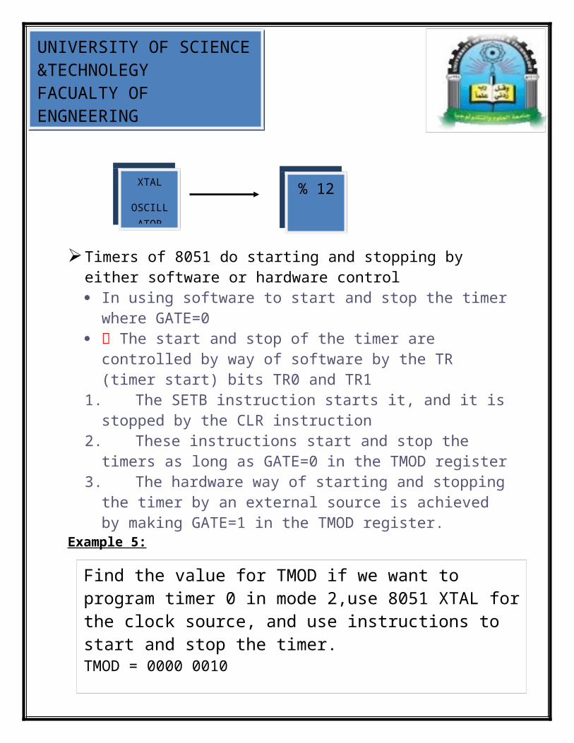
UNIVERSITY OF SCIENCE ampTECHNOLEGYFACUALTY OF ENGNEERINGBIOMEDICAL
13
Example 7In Example 7 calculate the frequency of the square wave generatedon pin P15SolutionIn the timer delay calculation of Example 7 we did not include theoverhead due to instruction in the loop To get a more accurate timing
Example 8Find the delay generated by timer 0 in the following code using bothof the Methods of Figure 9-4 Do not include the overhead due toinstruction CLR P23 Clear P23 MOV TMOD01 Timer 0 16-bitmode
UNIVERSITY OF SCIENCE ampTECHNOLEGYFACUALTY OF ENGNEERINGBIOMEDICAL
14
Example 8Find the delay generated by timer 0 in the following code using bothof the Methods of Figure 9-4 Do not include the overhead due toinstruction CLR P23 Clear P23 MOV TMOD01 Timer 0 16-bitmode
Example 8The following program generates a square wave on P15 continuouslyusing timer 1 for a time delay Find the frequency of the squarewave if XTAL = 110592 MHz In your calculation do not
UNIVERSITY OF SCIENCE ampTECHNOLEGYFACUALTY OF ENGNEERINGBIOMEDICAL
15
Example 8The following program generates a square wave on P15 continuouslyusing timer 1 for a time delay Find the frequency of the squarewave if XTAL = 110592 MHz In your calculation do not
UNIVERSITY OF SCIENCE ampTECHNOLEGYFACUALTY OF ENGNEERINGBIOMEDICAL
LAB Expeirment (4)
Main Topics LCD Pins DescriptionsLCD CommandsLCD Operations
Learning ObjectivesTasks
Upon Compliation this expeirment you will be able to
List reasons that LCD are gaging wide-spread usereplacing LEDrsquoS
Describe the function of the pins of atypical LCD List instruction command codes for programming an LCD Interface an LCD to the 8051 Program an LCD by sending data or commands to it from
8051
16
UNIVERSITY OF SCIENCE ampTECHNOLEGYFACUALTY OF ENGNEERINGBIOMEDICAL
INTERFACING LCD TO 8051
8051 LCD
5v
10k pot
LCD Operation
LCD is finding widespread use replacing LEDs1048707 The declining prices of LCD1048707 The ability to display numbers characters and graphics1048707 Incorporation of a refreshing controller into the LCD thereby relieving the CPU of the task of refreshing the LCD1048707 Ease of programming for characters and graphicsLCD PinDescriptions
17
P01
P07
P20
P21
P23
D0 Vcc
Vee
D7 Vss
RS RW E
UNIVERSITY OF SCIENCE ampTECHNOLEGYFACUALTY OF ENGNEERINGBIOMEDICAL
LCD Pin Descriptions
Pin Descriptions for LCD
pin symbol
IO Descriptions
1 vss -- Ground2 vcc -- +5V power supply3 Vee -- Power supply to control
contrast4 Rs I RS=0 to select command
registerRS=1 to select data register
5 rw I RW=0 for writeRW=1 for read
6 E IO Enable7 DB0 IO The 8-bit data bus
pin symbol
IO Descriptions
8 DB1 IO The 8-bit data bus9 DB2 IO The 8-bit data bus
10 DB3 IO The 8-bit data bus11 DB4 IO The 8-bit data bus12 DB5 IO The 8-bit data bus
18
UNIVERSITY OF SCIENCE ampTECHNOLEGYFACUALTY OF ENGNEERINGBIOMEDICAL
13 DB6 IO The 8-bit data bus14 DB7 IO The 8-bit data bus
LCD Command Codes
CODE(HEX)
Command to LCD Instruction Register
1 Clear display screen2 Return home4 Decrement cursor (shift cursor to left)6 Increment cursor (shift cursor to right)5 Shift display right7 Shift display left8 Display off cursor offA Display off cursor onC Display on cursor off
19
UNIVERSITY OF SCIENCE ampTECHNOLEGYFACUALTY OF ENGNEERINGBIOMEDICAL
CODE(HEX)
Command to LCD Instruction Register
E Display on cursor blinkingF Display on cursor blinking
10 Shift cursor position to left14 Shift cursor position to right18 Shift the entire display to the left1C Shift the entire display to the right80 Force cursor to beginning to 1st lineC0 Force cursor to beginning to 2nd line38 2 lines and 5x7 matrix
Sending Codes and Data to LCDs w Time Delay
20
To send any of the commands to the LCD make pin RS=0 For datamake RS=1 Then send a high-to-low pulse to the E pin to enable theinternal latch of the LCD This is shown in the code belowcalls a time delay before sending next datacommandP10-P17 are connected to LCD data pins D0-D7P20 is connected to RS pin of LCDP21 is connected to RW pin of LCDP22 is connected to E pin of LCDORGMOV A38H INIT LCD 2 LINES 5X7 MATRIXACALL COMNWRT call command subroutineACALL DELAY give LCD some timeMOV A0EH display on cursor onACALL COMNWRT call command subroutineACALL DELAY give LCD some timeMOV A01 clear LCDACALL COMNWRT call command subroutine
UNIVERSITY OF SCIENCE ampTECHNOLEGYFACUALTY OF ENGNEERINGBIOMEDICAL
21
ACALL DELAY give LCD some timeMOV A06H shift cursor rightACALL COMNWRT call command subroutineACALL DELAY give LCD some timeMOV A84H cursor at line 1 pos 4ACALL COMNWRT call command subroutineACALL DELAY give LCD some timeMOV ArsquoNrsquo display letter NACALL DATAWRT call display subroutineACALL DELAY give LCD some timeMOV ArsquoOrsquo display letter OACALL DATAWRT call display subroutineAGAIN SJMP AGAIN stay hereCOMNWRT send command to LCDMOV P1A copy reg A to port 1CLR P20 RS=0 for commandCLR P21 RW=0 for writeSETB P22 E=1 for high pulseCLR P22 E=0 for H-to-L pulseRETDATAWRT write data to LCDMOV P1A copy reg A to port 1CLR P20 RS=0 for commandCLR P21 RW=0 for writeSETB P22 E=1 for high pulseCLR P22 E=0 for H-to-L pulseRETDELAY MOV R350 50 or higher for fast CPUsHERE2 MOV R4255 R4 = 255HERE DJNZ R4HERE stay until R4 becomes 0DJNZ R3HERE2RETEND
UNIVERSITY OF SCIENCE ampTECHNOLEGYFACUALTY OF ENGNEERINGBIOMEDICAL
Sending Codes and Data to LCDs w Busy Flag
22
Check busy flag before sending data command to LCDp1=data pinP20 connected to RS pinP21 connected to RW pinP22 connected to E pinORGMOV A38H init LCD 2 lines 5x7 matrixACALL COMMAND issue commandMOV A0EH LCD on cursor onACALL COMMAND issue commandMOV A01H clear LCD commandACALL COMMAND issue commandMOV A06H shift cursor rightACALL COMMAND issue commandMOV A86H cursor line 1 pos 6ACALL COMMAND command subroutineMOV ArsquoNrsquo display letter NACALL DATA_DISPLAYMOV ArsquoOrsquo display letter OACALL DATA_DISPLAYHERESJMP HERE STAY HERE
UNIVERSITY OF SCIENCE ampTECHNOLEGYFACUALTY OF ENGNEERINGBIOMEDICAL
23
COMMANDACALL READY is LCD readyMOV P1A issue command codeCLR P20 RS=0 for commandCLR P21 RW=0 to write to LCDSETB P22 E=1 for H-to-L pulseCLR P22 E=0latch inRETDATA_DISPLAYACALL READY is LCD readyMOV P1A issue dataSETB P20 RS=1 for dataCLR P21 RW =0 to write to LCDSETB P22 E=1 for H-to-L pulseCLR P22 E=0latch inRETREADYSETB P17 make P17 input portCLR P20 RS=0 access command regSETB P21 RW=1 read command reg read command reg and check busy flagBACKSETB P22 E=1 for H-to-L pulseCLR P22 E=0 H-to-L pulseJB P17BACK stay until busy flag=0RETEND
- Microcontroller (1) Lab Manual
-
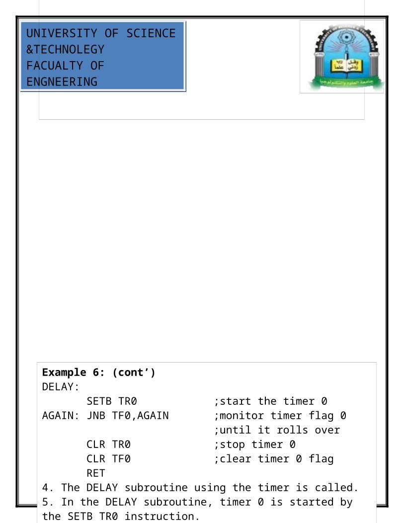
UNIVERSITY OF SCIENCE ampTECHNOLEGYFACUALTY OF ENGNEERINGBIOMEDICAL
14
Example 8Find the delay generated by timer 0 in the following code using bothof the Methods of Figure 9-4 Do not include the overhead due toinstruction CLR P23 Clear P23 MOV TMOD01 Timer 0 16-bitmode
Example 8The following program generates a square wave on P15 continuouslyusing timer 1 for a time delay Find the frequency of the squarewave if XTAL = 110592 MHz In your calculation do not
UNIVERSITY OF SCIENCE ampTECHNOLEGYFACUALTY OF ENGNEERINGBIOMEDICAL
15
Example 8The following program generates a square wave on P15 continuouslyusing timer 1 for a time delay Find the frequency of the squarewave if XTAL = 110592 MHz In your calculation do not
UNIVERSITY OF SCIENCE ampTECHNOLEGYFACUALTY OF ENGNEERINGBIOMEDICAL
LAB Expeirment (4)
Main Topics LCD Pins DescriptionsLCD CommandsLCD Operations
Learning ObjectivesTasks
Upon Compliation this expeirment you will be able to
List reasons that LCD are gaging wide-spread usereplacing LEDrsquoS
Describe the function of the pins of atypical LCD List instruction command codes for programming an LCD Interface an LCD to the 8051 Program an LCD by sending data or commands to it from
8051
16
UNIVERSITY OF SCIENCE ampTECHNOLEGYFACUALTY OF ENGNEERINGBIOMEDICAL
INTERFACING LCD TO 8051
8051 LCD
5v
10k pot
LCD Operation
LCD is finding widespread use replacing LEDs1048707 The declining prices of LCD1048707 The ability to display numbers characters and graphics1048707 Incorporation of a refreshing controller into the LCD thereby relieving the CPU of the task of refreshing the LCD1048707 Ease of programming for characters and graphicsLCD PinDescriptions
17
P01
P07
P20
P21
P23
D0 Vcc
Vee
D7 Vss
RS RW E
UNIVERSITY OF SCIENCE ampTECHNOLEGYFACUALTY OF ENGNEERINGBIOMEDICAL
LCD Pin Descriptions
Pin Descriptions for LCD
pin symbol
IO Descriptions
1 vss -- Ground2 vcc -- +5V power supply3 Vee -- Power supply to control
contrast4 Rs I RS=0 to select command
registerRS=1 to select data register
5 rw I RW=0 for writeRW=1 for read
6 E IO Enable7 DB0 IO The 8-bit data bus
pin symbol
IO Descriptions
8 DB1 IO The 8-bit data bus9 DB2 IO The 8-bit data bus
10 DB3 IO The 8-bit data bus11 DB4 IO The 8-bit data bus12 DB5 IO The 8-bit data bus
18
UNIVERSITY OF SCIENCE ampTECHNOLEGYFACUALTY OF ENGNEERINGBIOMEDICAL
13 DB6 IO The 8-bit data bus14 DB7 IO The 8-bit data bus
LCD Command Codes
CODE(HEX)
Command to LCD Instruction Register
1 Clear display screen2 Return home4 Decrement cursor (shift cursor to left)6 Increment cursor (shift cursor to right)5 Shift display right7 Shift display left8 Display off cursor offA Display off cursor onC Display on cursor off
19
UNIVERSITY OF SCIENCE ampTECHNOLEGYFACUALTY OF ENGNEERINGBIOMEDICAL
CODE(HEX)
Command to LCD Instruction Register
E Display on cursor blinkingF Display on cursor blinking
10 Shift cursor position to left14 Shift cursor position to right18 Shift the entire display to the left1C Shift the entire display to the right80 Force cursor to beginning to 1st lineC0 Force cursor to beginning to 2nd line38 2 lines and 5x7 matrix
Sending Codes and Data to LCDs w Time Delay
20
To send any of the commands to the LCD make pin RS=0 For datamake RS=1 Then send a high-to-low pulse to the E pin to enable theinternal latch of the LCD This is shown in the code belowcalls a time delay before sending next datacommandP10-P17 are connected to LCD data pins D0-D7P20 is connected to RS pin of LCDP21 is connected to RW pin of LCDP22 is connected to E pin of LCDORGMOV A38H INIT LCD 2 LINES 5X7 MATRIXACALL COMNWRT call command subroutineACALL DELAY give LCD some timeMOV A0EH display on cursor onACALL COMNWRT call command subroutineACALL DELAY give LCD some timeMOV A01 clear LCDACALL COMNWRT call command subroutine
UNIVERSITY OF SCIENCE ampTECHNOLEGYFACUALTY OF ENGNEERINGBIOMEDICAL
21
ACALL DELAY give LCD some timeMOV A06H shift cursor rightACALL COMNWRT call command subroutineACALL DELAY give LCD some timeMOV A84H cursor at line 1 pos 4ACALL COMNWRT call command subroutineACALL DELAY give LCD some timeMOV ArsquoNrsquo display letter NACALL DATAWRT call display subroutineACALL DELAY give LCD some timeMOV ArsquoOrsquo display letter OACALL DATAWRT call display subroutineAGAIN SJMP AGAIN stay hereCOMNWRT send command to LCDMOV P1A copy reg A to port 1CLR P20 RS=0 for commandCLR P21 RW=0 for writeSETB P22 E=1 for high pulseCLR P22 E=0 for H-to-L pulseRETDATAWRT write data to LCDMOV P1A copy reg A to port 1CLR P20 RS=0 for commandCLR P21 RW=0 for writeSETB P22 E=1 for high pulseCLR P22 E=0 for H-to-L pulseRETDELAY MOV R350 50 or higher for fast CPUsHERE2 MOV R4255 R4 = 255HERE DJNZ R4HERE stay until R4 becomes 0DJNZ R3HERE2RETEND
UNIVERSITY OF SCIENCE ampTECHNOLEGYFACUALTY OF ENGNEERINGBIOMEDICAL
Sending Codes and Data to LCDs w Busy Flag
22
Check busy flag before sending data command to LCDp1=data pinP20 connected to RS pinP21 connected to RW pinP22 connected to E pinORGMOV A38H init LCD 2 lines 5x7 matrixACALL COMMAND issue commandMOV A0EH LCD on cursor onACALL COMMAND issue commandMOV A01H clear LCD commandACALL COMMAND issue commandMOV A06H shift cursor rightACALL COMMAND issue commandMOV A86H cursor line 1 pos 6ACALL COMMAND command subroutineMOV ArsquoNrsquo display letter NACALL DATA_DISPLAYMOV ArsquoOrsquo display letter OACALL DATA_DISPLAYHERESJMP HERE STAY HERE
UNIVERSITY OF SCIENCE ampTECHNOLEGYFACUALTY OF ENGNEERINGBIOMEDICAL
23
COMMANDACALL READY is LCD readyMOV P1A issue command codeCLR P20 RS=0 for commandCLR P21 RW=0 to write to LCDSETB P22 E=1 for H-to-L pulseCLR P22 E=0latch inRETDATA_DISPLAYACALL READY is LCD readyMOV P1A issue dataSETB P20 RS=1 for dataCLR P21 RW =0 to write to LCDSETB P22 E=1 for H-to-L pulseCLR P22 E=0latch inRETREADYSETB P17 make P17 input portCLR P20 RS=0 access command regSETB P21 RW=1 read command reg read command reg and check busy flagBACKSETB P22 E=1 for H-to-L pulseCLR P22 E=0 H-to-L pulseJB P17BACK stay until busy flag=0RETEND
- Microcontroller (1) Lab Manual
-
UNIVERSITY OF SCIENCE ampTECHNOLEGYFACUALTY OF ENGNEERINGBIOMEDICAL
15
Example 8The following program generates a square wave on P15 continuouslyusing timer 1 for a time delay Find the frequency of the squarewave if XTAL = 110592 MHz In your calculation do not
UNIVERSITY OF SCIENCE ampTECHNOLEGYFACUALTY OF ENGNEERINGBIOMEDICAL
LAB Expeirment (4)
Main Topics LCD Pins DescriptionsLCD CommandsLCD Operations
Learning ObjectivesTasks
Upon Compliation this expeirment you will be able to
List reasons that LCD are gaging wide-spread usereplacing LEDrsquoS
Describe the function of the pins of atypical LCD List instruction command codes for programming an LCD Interface an LCD to the 8051 Program an LCD by sending data or commands to it from
8051
16
UNIVERSITY OF SCIENCE ampTECHNOLEGYFACUALTY OF ENGNEERINGBIOMEDICAL
INTERFACING LCD TO 8051
8051 LCD
5v
10k pot
LCD Operation
LCD is finding widespread use replacing LEDs1048707 The declining prices of LCD1048707 The ability to display numbers characters and graphics1048707 Incorporation of a refreshing controller into the LCD thereby relieving the CPU of the task of refreshing the LCD1048707 Ease of programming for characters and graphicsLCD PinDescriptions
17
P01
P07
P20
P21
P23
D0 Vcc
Vee
D7 Vss
RS RW E
UNIVERSITY OF SCIENCE ampTECHNOLEGYFACUALTY OF ENGNEERINGBIOMEDICAL
LCD Pin Descriptions
Pin Descriptions for LCD
pin symbol
IO Descriptions
1 vss -- Ground2 vcc -- +5V power supply3 Vee -- Power supply to control
contrast4 Rs I RS=0 to select command
registerRS=1 to select data register
5 rw I RW=0 for writeRW=1 for read
6 E IO Enable7 DB0 IO The 8-bit data bus
pin symbol
IO Descriptions
8 DB1 IO The 8-bit data bus9 DB2 IO The 8-bit data bus
10 DB3 IO The 8-bit data bus11 DB4 IO The 8-bit data bus12 DB5 IO The 8-bit data bus
18
UNIVERSITY OF SCIENCE ampTECHNOLEGYFACUALTY OF ENGNEERINGBIOMEDICAL
13 DB6 IO The 8-bit data bus14 DB7 IO The 8-bit data bus
LCD Command Codes
CODE(HEX)
Command to LCD Instruction Register
1 Clear display screen2 Return home4 Decrement cursor (shift cursor to left)6 Increment cursor (shift cursor to right)5 Shift display right7 Shift display left8 Display off cursor offA Display off cursor onC Display on cursor off
19
UNIVERSITY OF SCIENCE ampTECHNOLEGYFACUALTY OF ENGNEERINGBIOMEDICAL
CODE(HEX)
Command to LCD Instruction Register
E Display on cursor blinkingF Display on cursor blinking
10 Shift cursor position to left14 Shift cursor position to right18 Shift the entire display to the left1C Shift the entire display to the right80 Force cursor to beginning to 1st lineC0 Force cursor to beginning to 2nd line38 2 lines and 5x7 matrix
Sending Codes and Data to LCDs w Time Delay
20
To send any of the commands to the LCD make pin RS=0 For datamake RS=1 Then send a high-to-low pulse to the E pin to enable theinternal latch of the LCD This is shown in the code belowcalls a time delay before sending next datacommandP10-P17 are connected to LCD data pins D0-D7P20 is connected to RS pin of LCDP21 is connected to RW pin of LCDP22 is connected to E pin of LCDORGMOV A38H INIT LCD 2 LINES 5X7 MATRIXACALL COMNWRT call command subroutineACALL DELAY give LCD some timeMOV A0EH display on cursor onACALL COMNWRT call command subroutineACALL DELAY give LCD some timeMOV A01 clear LCDACALL COMNWRT call command subroutine
UNIVERSITY OF SCIENCE ampTECHNOLEGYFACUALTY OF ENGNEERINGBIOMEDICAL
21
ACALL DELAY give LCD some timeMOV A06H shift cursor rightACALL COMNWRT call command subroutineACALL DELAY give LCD some timeMOV A84H cursor at line 1 pos 4ACALL COMNWRT call command subroutineACALL DELAY give LCD some timeMOV ArsquoNrsquo display letter NACALL DATAWRT call display subroutineACALL DELAY give LCD some timeMOV ArsquoOrsquo display letter OACALL DATAWRT call display subroutineAGAIN SJMP AGAIN stay hereCOMNWRT send command to LCDMOV P1A copy reg A to port 1CLR P20 RS=0 for commandCLR P21 RW=0 for writeSETB P22 E=1 for high pulseCLR P22 E=0 for H-to-L pulseRETDATAWRT write data to LCDMOV P1A copy reg A to port 1CLR P20 RS=0 for commandCLR P21 RW=0 for writeSETB P22 E=1 for high pulseCLR P22 E=0 for H-to-L pulseRETDELAY MOV R350 50 or higher for fast CPUsHERE2 MOV R4255 R4 = 255HERE DJNZ R4HERE stay until R4 becomes 0DJNZ R3HERE2RETEND
UNIVERSITY OF SCIENCE ampTECHNOLEGYFACUALTY OF ENGNEERINGBIOMEDICAL
Sending Codes and Data to LCDs w Busy Flag
22
Check busy flag before sending data command to LCDp1=data pinP20 connected to RS pinP21 connected to RW pinP22 connected to E pinORGMOV A38H init LCD 2 lines 5x7 matrixACALL COMMAND issue commandMOV A0EH LCD on cursor onACALL COMMAND issue commandMOV A01H clear LCD commandACALL COMMAND issue commandMOV A06H shift cursor rightACALL COMMAND issue commandMOV A86H cursor line 1 pos 6ACALL COMMAND command subroutineMOV ArsquoNrsquo display letter NACALL DATA_DISPLAYMOV ArsquoOrsquo display letter OACALL DATA_DISPLAYHERESJMP HERE STAY HERE
UNIVERSITY OF SCIENCE ampTECHNOLEGYFACUALTY OF ENGNEERINGBIOMEDICAL
23
COMMANDACALL READY is LCD readyMOV P1A issue command codeCLR P20 RS=0 for commandCLR P21 RW=0 to write to LCDSETB P22 E=1 for H-to-L pulseCLR P22 E=0latch inRETDATA_DISPLAYACALL READY is LCD readyMOV P1A issue dataSETB P20 RS=1 for dataCLR P21 RW =0 to write to LCDSETB P22 E=1 for H-to-L pulseCLR P22 E=0latch inRETREADYSETB P17 make P17 input portCLR P20 RS=0 access command regSETB P21 RW=1 read command reg read command reg and check busy flagBACKSETB P22 E=1 for H-to-L pulseCLR P22 E=0 H-to-L pulseJB P17BACK stay until busy flag=0RETEND
- Microcontroller (1) Lab Manual
-

UNIVERSITY OF SCIENCE ampTECHNOLEGYFACUALTY OF ENGNEERINGBIOMEDICAL
13 DB6 IO The 8-bit data bus14 DB7 IO The 8-bit data bus
LCD Command Codes
CODE(HEX)
Command to LCD Instruction Register
1 Clear display screen2 Return home4 Decrement cursor (shift cursor to left)6 Increment cursor (shift cursor to right)5 Shift display right7 Shift display left8 Display off cursor offA Display off cursor onC Display on cursor off
19
UNIVERSITY OF SCIENCE ampTECHNOLEGYFACUALTY OF ENGNEERINGBIOMEDICAL
CODE(HEX)
Command to LCD Instruction Register
E Display on cursor blinkingF Display on cursor blinking
10 Shift cursor position to left14 Shift cursor position to right18 Shift the entire display to the left1C Shift the entire display to the right80 Force cursor to beginning to 1st lineC0 Force cursor to beginning to 2nd line38 2 lines and 5x7 matrix
Sending Codes and Data to LCDs w Time Delay
20
To send any of the commands to the LCD make pin RS=0 For datamake RS=1 Then send a high-to-low pulse to the E pin to enable theinternal latch of the LCD This is shown in the code belowcalls a time delay before sending next datacommandP10-P17 are connected to LCD data pins D0-D7P20 is connected to RS pin of LCDP21 is connected to RW pin of LCDP22 is connected to E pin of LCDORGMOV A38H INIT LCD 2 LINES 5X7 MATRIXACALL COMNWRT call command subroutineACALL DELAY give LCD some timeMOV A0EH display on cursor onACALL COMNWRT call command subroutineACALL DELAY give LCD some timeMOV A01 clear LCDACALL COMNWRT call command subroutine
UNIVERSITY OF SCIENCE ampTECHNOLEGYFACUALTY OF ENGNEERINGBIOMEDICAL
21
ACALL DELAY give LCD some timeMOV A06H shift cursor rightACALL COMNWRT call command subroutineACALL DELAY give LCD some timeMOV A84H cursor at line 1 pos 4ACALL COMNWRT call command subroutineACALL DELAY give LCD some timeMOV ArsquoNrsquo display letter NACALL DATAWRT call display subroutineACALL DELAY give LCD some timeMOV ArsquoOrsquo display letter OACALL DATAWRT call display subroutineAGAIN SJMP AGAIN stay hereCOMNWRT send command to LCDMOV P1A copy reg A to port 1CLR P20 RS=0 for commandCLR P21 RW=0 for writeSETB P22 E=1 for high pulseCLR P22 E=0 for H-to-L pulseRETDATAWRT write data to LCDMOV P1A copy reg A to port 1CLR P20 RS=0 for commandCLR P21 RW=0 for writeSETB P22 E=1 for high pulseCLR P22 E=0 for H-to-L pulseRETDELAY MOV R350 50 or higher for fast CPUsHERE2 MOV R4255 R4 = 255HERE DJNZ R4HERE stay until R4 becomes 0DJNZ R3HERE2RETEND
UNIVERSITY OF SCIENCE ampTECHNOLEGYFACUALTY OF ENGNEERINGBIOMEDICAL
Sending Codes and Data to LCDs w Busy Flag
22
Check busy flag before sending data command to LCDp1=data pinP20 connected to RS pinP21 connected to RW pinP22 connected to E pinORGMOV A38H init LCD 2 lines 5x7 matrixACALL COMMAND issue commandMOV A0EH LCD on cursor onACALL COMMAND issue commandMOV A01H clear LCD commandACALL COMMAND issue commandMOV A06H shift cursor rightACALL COMMAND issue commandMOV A86H cursor line 1 pos 6ACALL COMMAND command subroutineMOV ArsquoNrsquo display letter NACALL DATA_DISPLAYMOV ArsquoOrsquo display letter OACALL DATA_DISPLAYHERESJMP HERE STAY HERE
UNIVERSITY OF SCIENCE ampTECHNOLEGYFACUALTY OF ENGNEERINGBIOMEDICAL
23
COMMANDACALL READY is LCD readyMOV P1A issue command codeCLR P20 RS=0 for commandCLR P21 RW=0 to write to LCDSETB P22 E=1 for H-to-L pulseCLR P22 E=0latch inRETDATA_DISPLAYACALL READY is LCD readyMOV P1A issue dataSETB P20 RS=1 for dataCLR P21 RW =0 to write to LCDSETB P22 E=1 for H-to-L pulseCLR P22 E=0latch inRETREADYSETB P17 make P17 input portCLR P20 RS=0 access command regSETB P21 RW=1 read command reg read command reg and check busy flagBACKSETB P22 E=1 for H-to-L pulseCLR P22 E=0 H-to-L pulseJB P17BACK stay until busy flag=0RETEND
- Microcontroller (1) Lab Manual
-
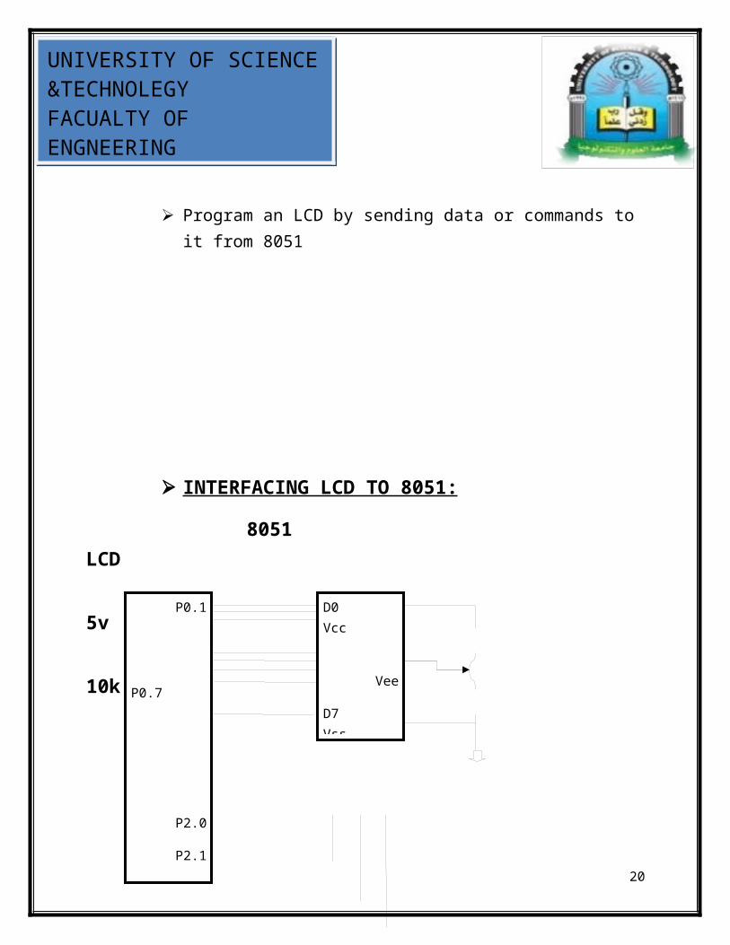
UNIVERSITY OF SCIENCE ampTECHNOLEGYFACUALTY OF ENGNEERINGBIOMEDICAL
21
ACALL DELAY give LCD some timeMOV A06H shift cursor rightACALL COMNWRT call command subroutineACALL DELAY give LCD some timeMOV A84H cursor at line 1 pos 4ACALL COMNWRT call command subroutineACALL DELAY give LCD some timeMOV ArsquoNrsquo display letter NACALL DATAWRT call display subroutineACALL DELAY give LCD some timeMOV ArsquoOrsquo display letter OACALL DATAWRT call display subroutineAGAIN SJMP AGAIN stay hereCOMNWRT send command to LCDMOV P1A copy reg A to port 1CLR P20 RS=0 for commandCLR P21 RW=0 for writeSETB P22 E=1 for high pulseCLR P22 E=0 for H-to-L pulseRETDATAWRT write data to LCDMOV P1A copy reg A to port 1CLR P20 RS=0 for commandCLR P21 RW=0 for writeSETB P22 E=1 for high pulseCLR P22 E=0 for H-to-L pulseRETDELAY MOV R350 50 or higher for fast CPUsHERE2 MOV R4255 R4 = 255HERE DJNZ R4HERE stay until R4 becomes 0DJNZ R3HERE2RETEND
UNIVERSITY OF SCIENCE ampTECHNOLEGYFACUALTY OF ENGNEERINGBIOMEDICAL
Sending Codes and Data to LCDs w Busy Flag
22
Check busy flag before sending data command to LCDp1=data pinP20 connected to RS pinP21 connected to RW pinP22 connected to E pinORGMOV A38H init LCD 2 lines 5x7 matrixACALL COMMAND issue commandMOV A0EH LCD on cursor onACALL COMMAND issue commandMOV A01H clear LCD commandACALL COMMAND issue commandMOV A06H shift cursor rightACALL COMMAND issue commandMOV A86H cursor line 1 pos 6ACALL COMMAND command subroutineMOV ArsquoNrsquo display letter NACALL DATA_DISPLAYMOV ArsquoOrsquo display letter OACALL DATA_DISPLAYHERESJMP HERE STAY HERE
UNIVERSITY OF SCIENCE ampTECHNOLEGYFACUALTY OF ENGNEERINGBIOMEDICAL
23
COMMANDACALL READY is LCD readyMOV P1A issue command codeCLR P20 RS=0 for commandCLR P21 RW=0 to write to LCDSETB P22 E=1 for H-to-L pulseCLR P22 E=0latch inRETDATA_DISPLAYACALL READY is LCD readyMOV P1A issue dataSETB P20 RS=1 for dataCLR P21 RW =0 to write to LCDSETB P22 E=1 for H-to-L pulseCLR P22 E=0latch inRETREADYSETB P17 make P17 input portCLR P20 RS=0 access command regSETB P21 RW=1 read command reg read command reg and check busy flagBACKSETB P22 E=1 for H-to-L pulseCLR P22 E=0 H-to-L pulseJB P17BACK stay until busy flag=0RETEND
- Microcontroller (1) Lab Manual
-
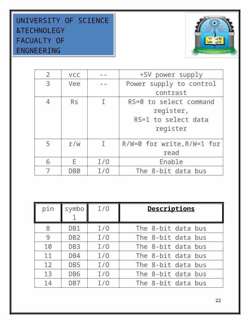
UNIVERSITY OF SCIENCE ampTECHNOLEGYFACUALTY OF ENGNEERINGBIOMEDICAL
23
COMMANDACALL READY is LCD readyMOV P1A issue command codeCLR P20 RS=0 for commandCLR P21 RW=0 to write to LCDSETB P22 E=1 for H-to-L pulseCLR P22 E=0latch inRETDATA_DISPLAYACALL READY is LCD readyMOV P1A issue dataSETB P20 RS=1 for dataCLR P21 RW =0 to write to LCDSETB P22 E=1 for H-to-L pulseCLR P22 E=0latch inRETREADYSETB P17 make P17 input portCLR P20 RS=0 access command regSETB P21 RW=1 read command reg read command reg and check busy flagBACKSETB P22 E=1 for H-to-L pulseCLR P22 E=0 H-to-L pulseJB P17BACK stay until busy flag=0RETEND
- Microcontroller (1) Lab Manual
-