micropower, low noise precision voltage references with shutdown
TRANSCRIPT
Micropower, Low Noise Precision Voltage References with Shutdown
ADR391/ADR392/ADR395
Rev. H Information furnished by Analog Devices is believed to be accurate and reliable. However, no responsibility is assumed by Analog Devices for its use, nor for any infringements of patents or other rights of third parties that may result from its use. Specifications subject to change without notice. No license is granted by implication or otherwise under any patent or patent rights of Analog Devices. Trademarks and registered trademarks are the property of their respective owners.
One Technology Way, P.O. Box 9106, Norwood, MA 02062-9106, U.S.A.Tel: 781.329.4700 www.analog.com Fax: 781.461.3113 ©2002–2009 Analog Devices, Inc. All rights reserved.
FEATURES Compact 5-lead TSOT package Low temperature coefficient
B grade: 9 ppm/°C A grade: 25 ppm/°C
Initial accuracy B grade: ±4 mV maximum (ADR391) A grade: ±6 mV maximum
Ultralow output noise: 5 μV p-p (0.1 Hz to 10 Hz) Low dropout: 300 mV Low supply current
3 μA maximum in shutdown 140 μA maximum in operation
No external capacitor required Output current: 5 mA Automotive grade available Wide temperature range: −40°C to +125°C
APPLICATIONS Battery-powered instrumentation Portable medical instrumentation Data acquisition systems Industrial process controls Automotive
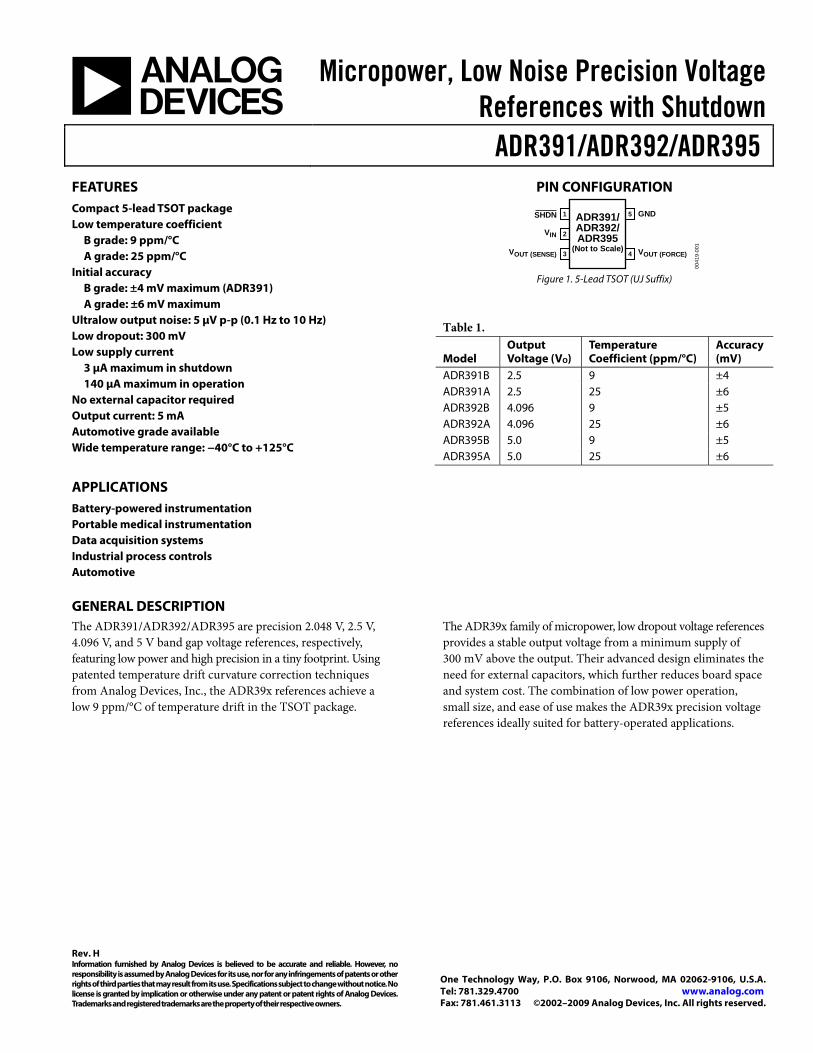
PIN CONFIGURATION
1
2
3
5
4
GNDSHDN
VOUT (SENSE) VOUT (FORCE)
VIN
0041
9-00
1
ADR391/ADR392/ADR395
(Not to Scale)
Figure 1. 5-Lead TSOT (UJ Suffix)
Table 1.
Model Output Voltage (VO)
Temperature Coefficient (ppm/°C)
Accuracy (mV)
ADR391B 2.5 9 ±4 ADR391A 2.5 25 ±6 ADR392B 4.096 9 ±5 ADR392A 4.096 25 ±6 ADR395B 5.0 9 ±5 ADR395A 5.0 25 ±6
GENERAL DESCRIPTION The ADR391/ADR392/ADR395 are precision 2.048 V, 2.5 V, 4.096 V, and 5 V band gap voltage references, respectively, featuring low power and high precision in a tiny footprint. Using patented temperature drift curvature correction techniques from Analog Devices, Inc., the ADR39x references achieve a low 9 ppm/°C of temperature drift in the TSOT package.
The ADR39x family of micropower, low dropout voltage references provides a stable output voltage from a minimum supply of 300 mV above the output. Their advanced design eliminates the need for external capacitors, which further reduces board space and system cost. The combination of low power operation, small size, and ease of use makes the ADR39x precision voltage references ideally suited for battery-operated applications.
ADR391/ADR392/ADR395
Rev. H | Page 2 of 20
TABLE OF CONTENTS Features .............................................................................................. 1
Applications ....................................................................................... 1
Pin Configuration ............................................................................. 1
General Description ......................................................................... 1
Revision History ............................................................................... 2
Specifications ..................................................................................... 3
ADR391 Electrical Characteristics ............................................. 3
ADR392 Electrical Characteristics ............................................. 4
ADR395 Electrical Characteristics ............................................. 5
Absolute Maximum Ratings ............................................................ 6
Thermal Resistance ...................................................................... 6
ESD Caution...................................................................................6
Typical Performance Characteristics ..............................................7
Terminology .................................................................................... 13
Theory of Operation ...................................................................... 14
Device Power Dissipation Considerations .............................. 14
Shutdown Mode Operation ...................................................... 14
Applications Information .............................................................. 15
Basic Voltage Reference Connection ....................................... 15
Capacitors .................................................................................... 17
Outline Dimensions ....................................................................... 18
Ordering Guide .......................................................................... 18
REVISION HISTORY 10/09—Rev. G to Rev. H Deleted ADR390 ................................................................. Universal Changes to Ordering Guide Section ............................................ 18 2/08—Rev. F to Rev. G Changes to Ripple Rejection Ration Parameter (Table 2) ........... 3 Changes to Ripple Rejection Ration Parameter (Table 3) ........... 4 Changes to Ripple Rejection Ration Parameter (Table 4) ........... 5 Changes to Ripple Rejection Ration Parameter (Table 5) ........... 6 Changes to Figure 7 .......................................................................... 9 Changes to Outline Dimensions ................................................... 19 Changes to Ordering Guide .......................................................... 19 5/05—Rev. E to Rev. F Changes to Table 5 ............................................................................ 7 Changes to Figure 2 .......................................................................... 9 4/04—Rev. D to Rev. E Changes to ADR390—Specifications ............................................. 3 Changes to ADR391—Specifications ............................................. 4 Changes to ADR392—Specifications ............................................. 5 Changes to ADR395—Specifications ............................................. 6 4/04—Rev. C to Rev. D Updated Format .................................................................. Universal Changes to Title ................................................................................ 1 Changes to Features .......................................................................... 1 Changes to Applications .................................................................. 1 Changes to General Description .................................................... 1 Changes to Table 1 ............................................................................ 1 Changes to ADR390—Specifications ............................................. 3 Changes to ADR391—Specifications ............................................. 4
Changes to ADR392—Specifications ............................................. 5 Changes to ADR395—Specifications ............................................. 6 Changes to Absolute Maximum Ratings ........................................ 7 Changes to Thermal Resistance....................................................... 7 Moved ESD Caution.......................................................................... 7 Changes to Figure 3, Figure 4, Figure 7, and Figure 8 .................. 9 Changes to Figure 11, Figure 12, Figure 13, and Figure 14....... 10 Changes to Figure 15, Figure 16, Figure 19, and Figure 20....... 11 Changes to Figure 23 and Figure 24............................................. 12 Changes to Figure 27 ...................................................................... 13 Changes to Ordering Guide .......................................................... 19 Updated Outline Dimensions ....................................................... 19 10/02—Rev. B to Rev. C Add parts ADR392 and ADR395 ..................................... Universal Changes to Features .......................................................................... 1 Changes to General Description ..................................................... 1 Additions to Table I ........................................................................... 1 Changes to Specifications ................................................................. 2 Changes to Ordering Guide ............................................................. 4 Changes to Absolute Maximum Ratings ........................................ 4 New TPCs 3, 4, 7, 8, 11, 12, 15, 16, 19, and 20 .............................. 6 New Figures 4 and 5 ....................................................................... 13 Deleted A Negative Precision Reference without Precision Resistors Section ............................................. 13 Edits to General-Purpose Current Source Section .................... 13 Updated Outline Dimensions ....................................................... 15 5/02—Rev. A to Rev. B Edits to Layout .................................................................... Universal Changes to Figure 6 ........................................................................ 13
ADR391/ADR392/ADR395
Rev. H | Page 3 of 20
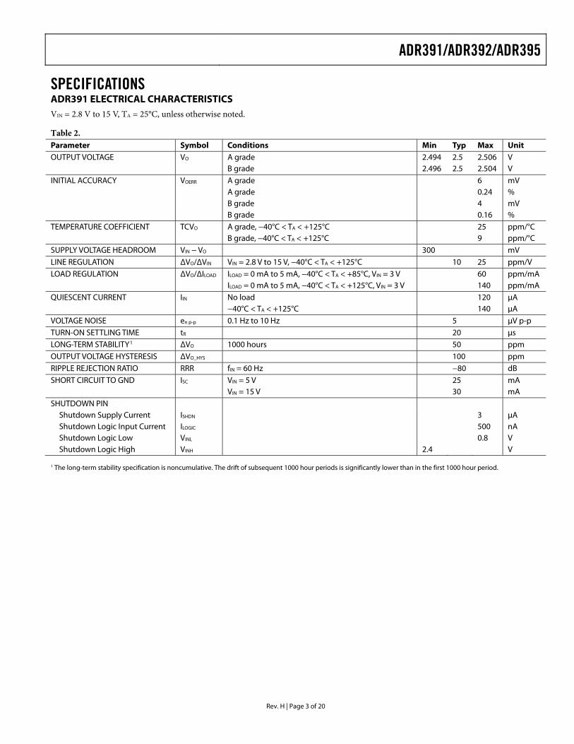
SPECIFICATIONS ADR391 ELECTRICAL CHARACTERISTICS VIN = 2.8 V to 15 V, TA = 25°C, unless otherwise noted.
Table 2. Parameter Symbol Conditions Min Typ Max Unit OUTPUT VOLTAGE VO A grade 2.494 2.5 2.506 V B grade 2.496 2.5 2.504 V INITIAL ACCURACY VOERR A grade 6 mV A grade 0.24 % B grade 4 mV B grade 0.16 % TEMPERATURE COEFFICIENT TCVO A grade, −40°C < TA < +125°C 25 ppm/°C B grade, −40°C < TA < +125°C 9 ppm/°C SUPPLY VOLTAGE HEADROOM VIN − VO 300 mV LINE REGULATION ΔVO/ΔVIN VIN = 2.8 V to 15 V, −40°C < TA < +125°C 10 25 ppm/V LOAD REGULATION ΔVO/ΔILOAD ILOAD = 0 mA to 5 mA, −40°C < TA < +85°C, VIN = 3 V 60 ppm/mA ILOAD = 0 mA to 5 mA, −40°C < TA < +125°C, VIN = 3 V 140 ppm/mA QUIESCENT CURRENT IIN No load 120 μA −40°C < TA < +125°C 140 μA VOLTAGE NOISE en p-p 0.1 Hz to 10 Hz 5 μV p-p TURN-ON SETTLING TIME tR 20 μs LONG-TERM STABILITY1 ΔVO 1000 hours 50 ppm OUTPUT VOLTAGE HYSTERESIS ΔVO_HYS 100 ppm RIPPLE REJECTION RATIO RRR fIN = 60 Hz −80 dB SHORT CIRCUIT TO GND ISC VIN = 5 V 25 mA VIN = 15 V 30 mA SHUTDOWN PIN
Shutdown Supply Current ISHDN 3 μA Shutdown Logic Input Current ILOGIC 500 nA Shutdown Logic Low VINL 0.8 V Shutdown Logic High VINH 2.4 V
1 The long-term stability specification is noncumulative. The drift of subsequent 1000 hour periods is significantly lower than in the first 1000 hour period.

ADR391/ADR392/ADR395
Rev. H | Page 4 of 20
ADR392 ELECTRICAL CHARACTERISTICS VIN = 4.3 V to 15 V, TA = 25°C, unless otherwise noted.
Table 3. Parameter Symbol Conditions Min Typ Max Unit OUTPUT VOLTAGE VO A grade 4.090 4.096 4.102 V B grade 4.091 4.096 4.101 V INITIAL ACCURACY VOERR A grade 6 mV A grade 0.15 % B grade 5 mV B grade 0.12 % TEMPERATURE COEFFICIENT TCVO A grade, −40°C < TA < +125°C 25 ppm/°C B grade, −40°C < TA < +125°C 9 ppm/°C SUPPLY VOLTAGE HEADROOM VIN − VO 300 mV LINE REGULATION ΔVO/ΔVIN VIN = 4.3 V to 15 V, −40°C < TA < +125°C 10 25 ppm/V LOAD REGULATION ΔVO/ΔILOAD ILOAD = 0 mA to 5 mA, −40°C < TA < +125°C, VIN = 5 V 140 ppm/mA QUIESCENT CURRENT IIN No load 120 μA −40°C < TA < +125°C 140 μA VOLTAGE NOISE en p-p 0.1 Hz to 10 Hz 7 μV p-p TURN-ON SETTLING TIME tR 20 μs LONG-TERM STABILITY1 ΔVO 1000 hours 50 ppm OUTPUT VOLTAGE HYSTERESIS ΔVO_HYS 100 ppm RIPPLE REJECTION RATIO RRR fIN = 60 Hz −80 dB SHORT CIRCUIT TO GND ISC VIN = 5 V 25 mA VIN = 15 V 30 mA SHUTDOWN PIN
Shutdown Supply Current ISHDN 3 μA Shutdown Logic Input Current ILOGIC 500 nA Shutdown Logic Low VINL 0.8 V Shutdown Logic High VINH 2.4 V
1 The long-term stability specification is noncumulative. The drift of subsequent 1000 hour periods is significantly lower than in the first 1000 hour period.
ADR391/ADR392/ADR395
Rev. H | Page 5 of 20
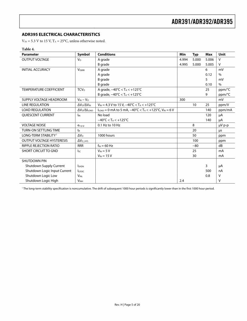
ADR395 ELECTRICAL CHARACTERISTICS VIN = 5.3 V to 15 V, TA = 25°C, unless otherwise noted.
Table 4. Parameter Symbol Conditions Min Typ Max Unit OUTPUT VOLTAGE VO A grade 4.994 5.000 5.006 V B grade 4.995 5.000 5.005 V INITIAL ACCURACY VOERR A grade 6 mV A grade 0.12 % B grade 5 mV B grade 0.10 % TEMPERATURE COEFFICIENT TCVO A grade, −40°C < TA < +125°C 25 ppm/°C B grade, −40°C < TA < +125°C 9 ppm/°C SUPPLY VOLTAGE HEADROOM VIN − VO 300 mV LINE REGULATION ΔVO/ΔVIN VIN = 4.3 V to 15 V, −40°C < TA < +125°C 10 25 ppm/V LOAD REGULATION ΔVO/ΔILOAD ILOAD = 0 mA to 5 mA, −40°C < TA < +125°C, VIN = 6 V 140 ppm/mA QUIESCENT CURRENT IIN No load 120 μA −40°C < TA < +125°C 140 μA VOLTAGE NOISE en p-p 0.1 Hz to 10 Hz 8 μV p-p TURN-ON SETTLING TIME tR 20 μs LONG-TERM STABILITY1 ΔVO 1000 hours 50 ppm OUTPUT VOLTAGE HYSTERESIS ΔVO_HYS 100 ppm RIPPLE REJECTION RATIO RRR fIN = 60 Hz −80 dB SHORT CIRCUIT TO GND ISC VIN = 5 V 25 mA VIN = 15 V 30 mA SHUTDOWN PIN
Shutdown Supply Current ISHDN 3 μA Shutdown Logic Input Current ILOGIC 500 nA Shutdown Logic Low VINL 0.8 V Shutdown Logic High VINH 2.4 V
1 The long-term stability specification is noncumulative. The drift of subsequent 1000 hour periods is significantly lower than in the first 1000 hour period.
ADR391/ADR392/ADR395
Rev. H | Page 6 of 20
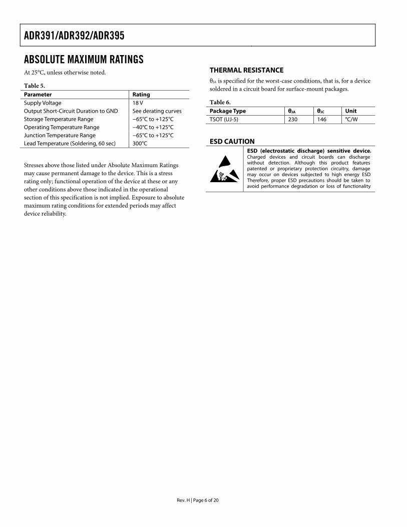
ABSOLUTE MAXIMUM RATINGS At 25°C, unless otherwise noted.
Table 5. Parameter Rating Supply Voltage 18 V Output Short-Circuit Duration to GND See derating curves Storage Temperature Range −65°C to +125°C Operating Temperature Range −40°C to +125°C Junction Temperature Range −65°C to +125°C Lead Temperature (Soldering, 60 sec) 300°C
Stresses above those listed under Absolute Maximum Ratings may cause permanent damage to the device. This is a stress rating only; functional operation of the device at these or any other conditions above those indicated in the operational section of this specification is not implied. Exposure to absolute maximum rating conditions for extended periods may affect device reliability.
THERMAL RESISTANCE θJA is specified for the worst-case conditions, that is, for a device soldered in a circuit board for surface-mount packages.
Table 6. Package Type θJA θJC Unit TSOT (UJ-5) 230 146 °C/W
ESD CAUTION

ADR391/ADR392/ADR395
Rev. H | Page 7 of 20
TYPICAL PERFORMANCE CHARACTERISTICS
2.494–40 –5 30 65 100 125
2.496
2.498
2.500
2.502
2.504
2.506
SAMPLE 1
SAMPLE 2
SAMPLE 3
TEMPERATURE (°C)
V OU
T (V
)
0041
9-00
4
Figure 2. ADR391 Output Voltage (VOUT) vs. Temperature
4.100
–40 0 40 80 125
4.098
4.096
4.094
4.090
4.088
4.092
SAMPLE 1
SAMPLE 2
SAMPLE 3
TEMPERATURE (°C)
V OU
T (V
)
0041
9-00
5
Figure 3. ADR392 Output Voltage (VOUT) vs. Temperature
5.006
–40 –5 30 65 125
5.004
5.002
5.000
4.996
4.994
4.998
100
SAMPLE 1
SAMPLE 2
SAMPLE 3
TEMPERATURE (°C)
V OU
T (V
)
0041
9-00
6
Figure 4. ADR395 Output Voltage (VOUT) vs. Temperature
INPUT VOLTAGE (V)
140
120
402.5 15.05.0
SUPP
LY C
UR
REN
T (µ
A)
7.5 10.0 12.5
100
80
60
+85°C
+25°C
–40°C
0041
9-00
8
+125°C
Figure 5. ADR391 Supply Current vs. Input Voltage
INPUT VOLTAGE (V)
140
5 7 9 11
SUPP
LY C
UR
REN
T (µ
A)
120
100
60
40
80
13 15
+125°C
+25°C
–40°C
0041
9-00
9
Figure 6. ADR392 Supply Current vs. Input Voltage
INPUT VOLTAGE (V)
140
5.5 7.0 8.5 10.0 14.5
SUPP
LY C
UR
REN
T (µ
A)
120
100
60
40
80
13.0
+125°C
+25°C
–40°C
11.5
0041
9-01
0
Figure 7. ADR395 Supply Current vs. Input Voltage
ADR391/ADR392/ADR395
Rev. H | Page 8 of 20
TEMPERATURE (°C)
80–40 –10
LOA
D R
EGU
LATI
ON
(ppm
/mA
)
50 80 110 125
100
120
140
160
180
20
IL = 0mA TO 5mA
VIN = 3V
VIN = 5V
0041
9-01
2
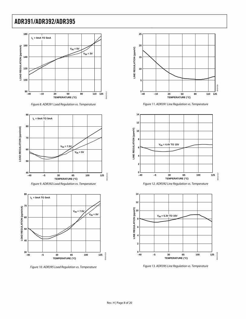
Figure 8. ADR391 Load Regulation vs. Temperature
TEMPERATURE (°C)
90
–40 –5 30 65 125
LOA
D R
EGU
LATI
ON
(ppm
/mA
) 80
70
50
40
60
100
IL = 0mA TO 5mA
VIN = 7.5V
VIN = 5V
0041
9-01
3
Figure 9. ADR392 Load Regulation vs. Temperature
TEMPERATURE (°C)
80
–40 –5 30 65 125
LOA
D R
EGU
LATI
ON
(ppm
/mA
) 70
60
40
30
50
100
IL = 0mA TO 5mA
VIN = 7.5VVIN = 5V
0041
9-01
4
Figure 10. ADR395 Load Regulation vs. Temperature
TEMPERATURE (°C)
0
LIN
E R
EGU
LATI
ON
(ppm
/V)
25
5
10
15
20
0041
9-01
6
–40 –10 20 80 110 12550
Figure 11. ADR391 Line Regulation vs. Temperature
TEMPERATURE (°C)
14
–40 –5 30 65 125
LIN
E R
EGU
LATI
ON
(ppm
/V)
10
6
2
0
4
100
12
8
VIN = 4.4V TO 15V
0041
9-01
7
Figure 12. ADR392 Line Regulation vs. Temperature
TEMPERATURE (°C)
14
–40 –5 30 65 125
LIN
E R
EGU
LATI
ON
(ppm
/V)
10
6
2
0
4
100
12
8VIN = 5.3V TO 15V
0041
9-01
8
Figure 13. ADR395 Line Regulation vs. Temperature
ADR391/ADR392/ADR395
Rev. H | Page 9 of 20
LOAD CURRENT (mA)
3.6
2.60 1
3.4
3.2
2.8
–40°C
+85°C
+25°C
2 3 4 5
3.0
+125°C
0041
9-02
0
V IN
MIN
(V)
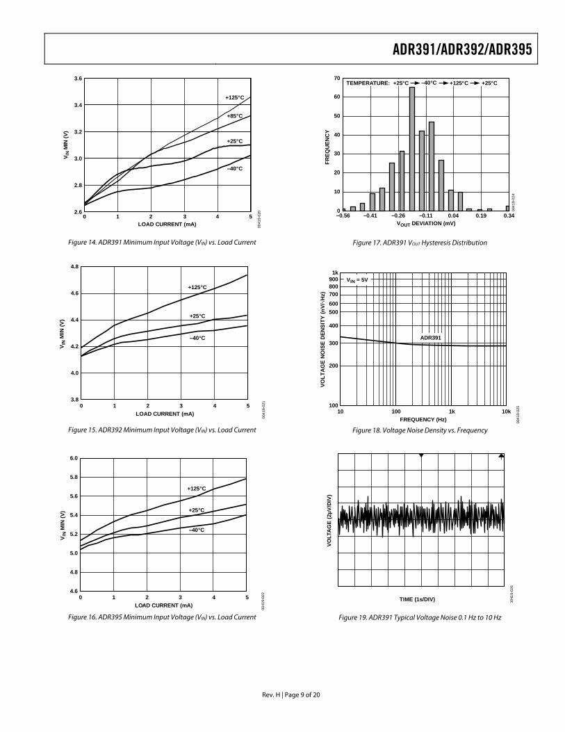
Figure 14. ADR391 Minimum Input Voltage (VIN) vs. Load Current
LOAD CURRENT (mA)
4.8
0 1 2 3 5
V IN
MIN
(V) 4.4
4.0
3.8
4.2
4
4.6+125°C
+25°C
–40°C
0041
9-02
1
Figure 15. ADR392 Minimum Input Voltage (VIN) vs. Load Current
LOAD CURRENT (mA)
6.0
0 1 2 3 5
V IN
MIN
(V)
5.2
4.8
4.6
5.0
4
5.6+125°C
+25°C
–40°C
5.8
5.4
0041
9-02
2
Figure 16. ADR395 Minimum Input Voltage (VIN) vs. Load Current
70
50
0–0.56 –0.26
FREQ
UEN
CY
0.04 0.19
40
30
20
10
–0.41 –0.11 0.34
60
TEMPERATURE: +25°C –40°C +125°C +25°C
0041
9-02
4
VOUT DEVIATION (mV)
Figure 17. ADR391 VOUT Hysteresis Distribution
1k900800700600
10010 100 1k 10k
FREQUENCY (Hz)
VOLT
AG
E N
OIS
E D
ENSI
TY (n
V/√H
z)
500
400
300
200
ADR391
VIN = 5V
0041
9-02
5
Figure 18. Voltage Noise Density vs. Frequency
VOLT
AG
E (2
µV/D
IV)
TIME (1s/DIV)
0
0
0
0
0
0
0
0
0
0041
9-02
6
Figure 19. ADR391 Typical Voltage Noise 0.1 Hz to 10 Hz
ADR391/ADR392/ADR395
Rev. H | Page 10 of 20
VOLT
AG
E (1
00µV
/DIV
)
TIME (10µs/DIV)
0041
9-02
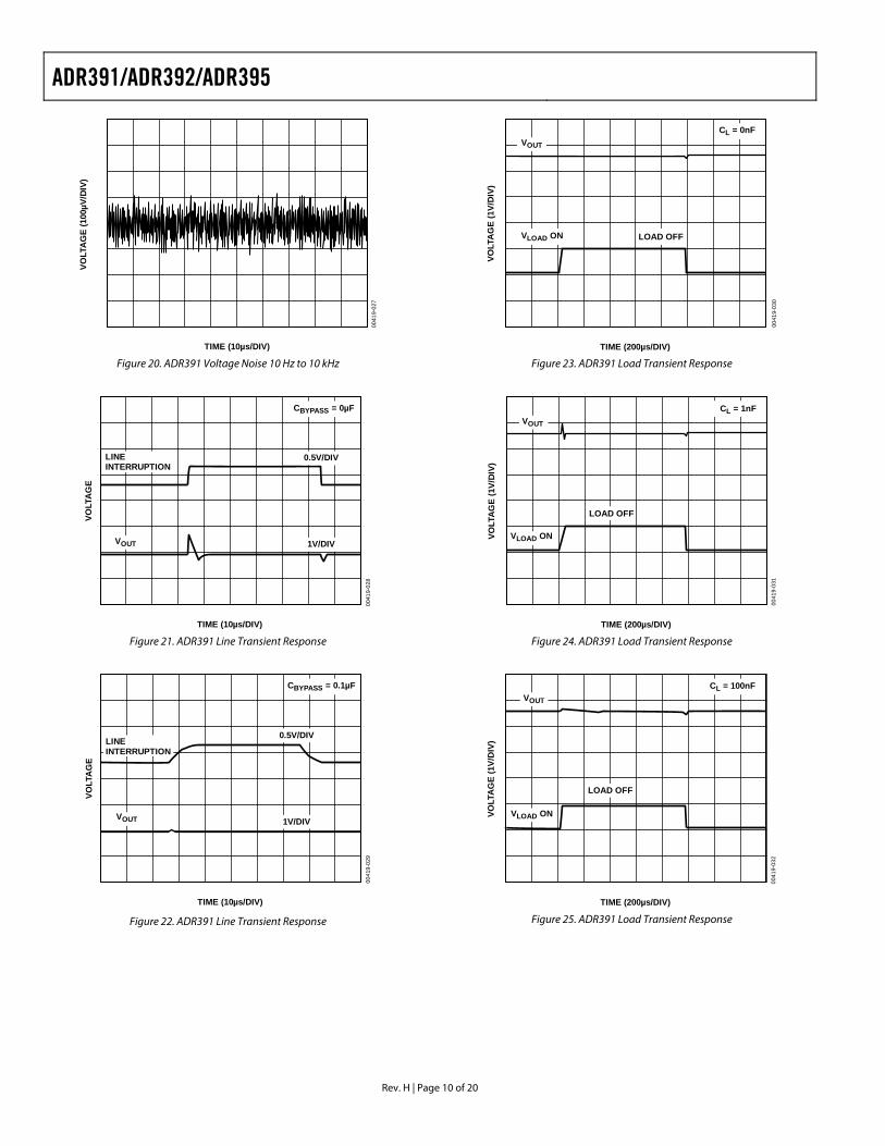
7Figure 20. ADR391 Voltage Noise 10 Hz to 10 kHz
VOLT
AG
E
TIME (10µs/DIV)
0.5V/DIV
1V/DIV
0041
9-02
8
LINEINTERRUPTION
VOUT
CBYPASS = 0µF
Figure 21. ADR391 Line Transient Response
VOLT
AG
E
TIME (10µs/DIV)
0.5V/DIV
1V/DIV
0041
9-02
9
LINEINTERRUPTION
VOUT
CBYPASS = 0.1µF
Figure 22. ADR391 Line Transient Response
VOLT
AG
E (1
V/D
IV)
TIME (200µs/DIV)
LOAD OFF
0041
9-03
0
VOUT
CL = 0nF
VLOAD ON
Figure 23. ADR391 Load Transient Response
VOLT
AG
E (1
V/D
IV)
TIME (200µs/DIV)
LOAD OFF
0041
9-03
1
VOUT
CL = 1nF
VLOAD ON
Figure 24. ADR391 Load Transient Response
VOLT
AG
E (1
V/D
IV)
TIME (200µs/DIV)
LOAD OFF
0041
9-03
2
VOUT
CL = 100nF
VLOAD ON
Figure 25. ADR391 Load Transient Response
ADR391/ADR392/ADR395
Rev. H | Page 11 of 20
VOLT
AG
E
TIME (20µs/DIV)
5V/DIV
2V/DIV
0041
9-03
3
VIN = 15V
VIN
VOUT
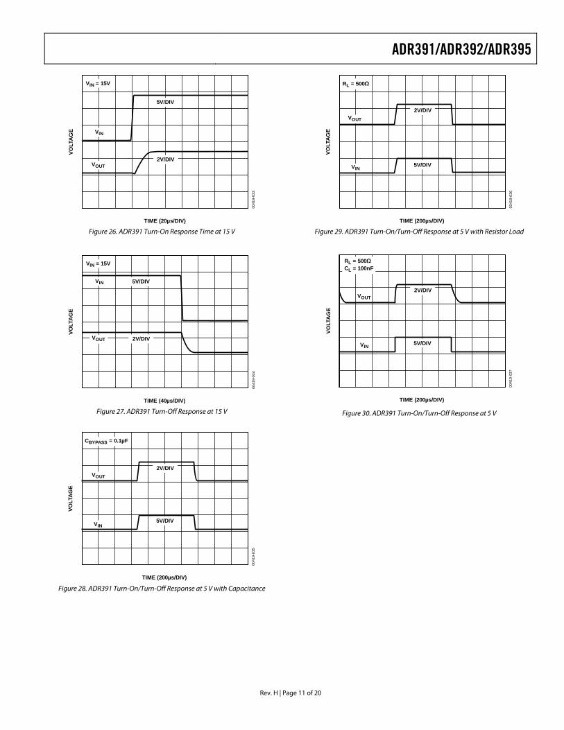
Figure 26. ADR391 Turn-On Response Time at 15 V
VOLT
AG
E
TIME (40µs/DIV)
5V/DIV
2V/DIV
0041
9-03
4
VIN = 15V
VIN
VOUT
Figure 27. ADR391 Turn-Off Response at 15 V
VOLT
AG
E
TIME (200µs/DIV)
5V/DIV
2V/DIV
0041
9-03
5
CBYPASS = 0.1µF
VIN
VOUT
Figure 28. ADR391 Turn-On/Turn-Off Response at 5 V with Capacitance
VOLT
AG
E
TIME (200µs/DIV)
5V/DIV
2V/DIV
0041
9-03
6
RL = 500Ω
VIN
VOUT
Figure 29. ADR391 Turn-On/Turn-Off Response at 5 V with Resistor Load
VOLT
AG
E
TIME (200µs/DIV)
5V/DIV
2V/DIV
0041
9-03
7
RL = 500ΩCL = 100nF
VIN
VOUT
Figure 30. ADR391 Turn-On/Turn-Off Response at 5 V
ADR391/ADR392/ADR395
Rev. H | Page 12 of 20
FREQUENCY (Hz)10 1M100
OU
TPU
T IM
PED
AN
CE
(Ω)
1k 10k 100k
100
90
0
80
70
60
50
40
30
20
10
0041
9-03
9
CL = 0µF
CL = 1µF CL = 0.1µF
FREQUENCY (Hz)10 1M100
RIP
PLE
REJ
ECTI
ON
(dB
)
1k 10k 100k
80
60
–120
40
20
0
–20
–40
–60
–80
–100
0041
9-03
8
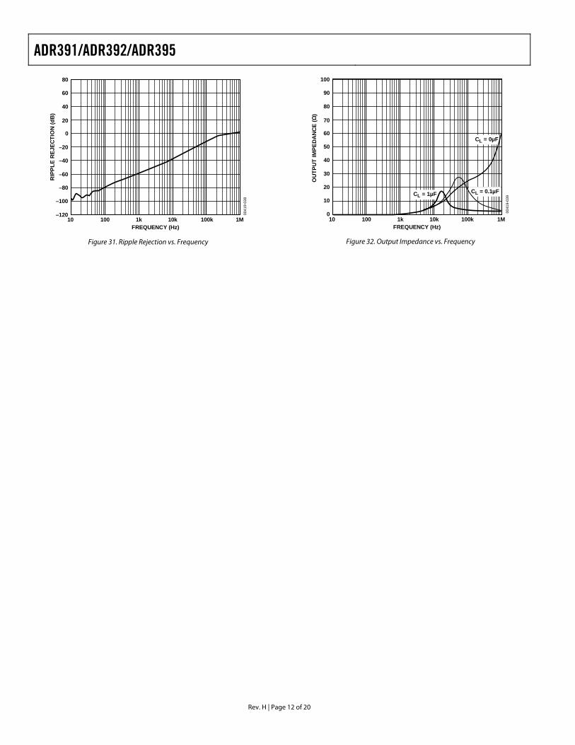
Figure 32. Output Impedance vs. Frequency
Figure 31. Ripple Rejection vs. Frequency
ADR391/ADR392/ADR395
Rev. H | Page 13 of 20
TERMINOLOGY Temperature Coefficient The change of output voltage with respect to operating temperature changes normalized by the output voltage at 25°C. This parameter is expressed in ppm/°C and can be determined by
[ ] ( ) ( )( ) ( )
610–C25
–Cppm/ ×
×°=°
12O
1O2OO TTV
TVTVTCV (1)
where: VO (25°C) is VO at 25°C. VO (T1) is VO at Temperature 1. VO (T2) is VO at Temperature 2.
Line Regulation The change in output voltage due to a specified change in input voltage. This parameter accounts for the effects of self-heating. Line regulation is expressed in either percent per volt, parts-per-million per volt, or microvolts per volt change in input voltage.
Load Regulation The change in output voltage due to a specified change in load current. This parameter accounts for the effects of self-heating. Load regulation is expressed in either microvolts per milliampere, parts-per-million per milliampere, or ohms of dc output resistance.
Long-Term Stability Typical shift of output voltage at 25°C on a sample of parts subjected to a test of 1000 hours at 25°C.
ΔVO = VO(t0) − VO(t1)
⎟⎟⎠
⎞⎜⎜⎝
⎛×
−=Δ 610
)()()(
]ppm[0O
1O0OO tV
tVtVV (2)
where: VO (t0) is VO at 25°C at Time 0. VO (t1) is VO at 25°C after 1000 hours operation at 25°C.
Thermally Induced Output Voltage Hysteresis The change of output voltage after the device cycles through the temperatures from +25°C to –40°C to +125°C and back to +25°C. This is a typical value from a sample of parts put through such a cycle.
VO_HYS = VO(25°C) − VO_TC (3)
6__ 10
)25()25(
]ppm[ ×−
=CVVCV
VO
TCOOHYSO o
o
(4)
where: VO (25°C) is VO at 25°C. VO_TC is VO at 25°C after a temperature cycle from +25°C to −40°C to +125°C and back to +25°C.
ADR391/ADR392/ADR395
Rev. H | Page 14 of 20
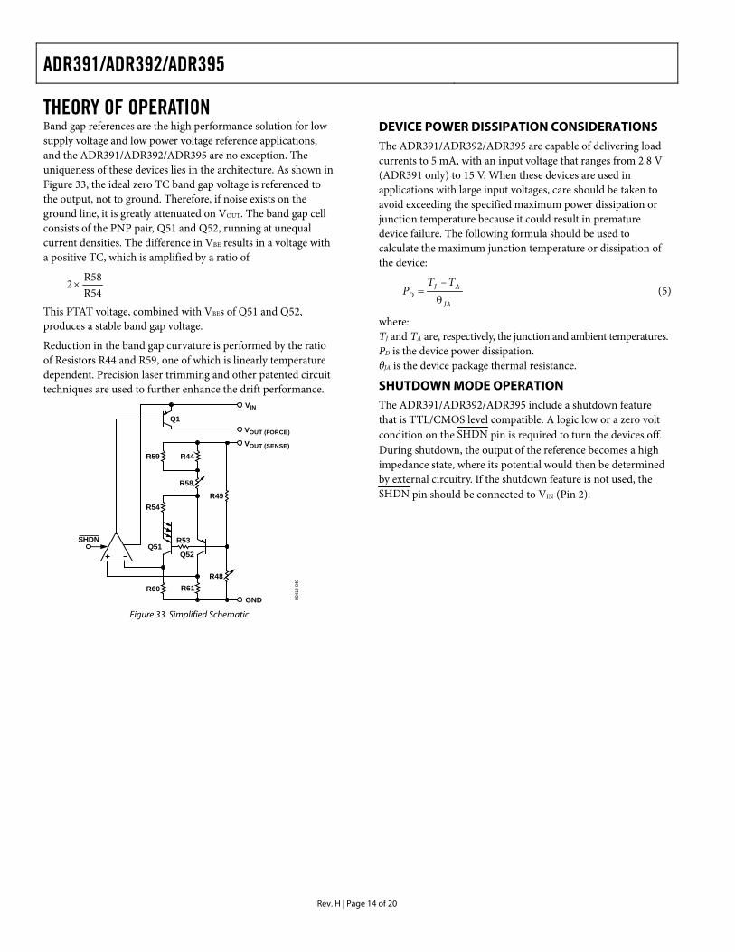
THEORY OF OPERATION Band gap references are the high performance solution for low supply voltage and low power voltage reference applications, and the ADR391/ADR392/ADR395 are no exception. The uniqueness of these devices lies in the architecture. As shown in Figure 33, the ideal zero TC band gap voltage is referenced to the output, not to ground. Therefore, if noise exists on the ground line, it is greatly attenuated on VOUT. The band gap cell consists of the PNP pair, Q51 and Q52, running at unequal current densities. The difference in VBE results in a voltage with a positive TC, which is amplified by a ratio of
R54R582×
This PTAT voltage, combined with VBEs of Q51 and Q52, produces a stable band gap voltage.
Reduction in the band gap curvature is performed by the ratio of Resistors R44 and R59, one of which is linearly temperature dependent. Precision laser trimming and other patented circuit techniques are used to further enhance the drift performance.
SHDN
R60
Q51
R54
R61
R53
Q52
R58
R59 R44
R48
R49
Q1
GND 0041
9-04
0
VIN
VOUT (FORCE)
VOUT (SENSE)
Figure 33. Simplified Schematic
DEVICE POWER DISSIPATION CONSIDERATIONS The ADR391/ADR392/ADR395 are capable of delivering load currents to 5 mA, with an input voltage that ranges from 2.8 V (ADR391 only) to 15 V. When these devices are used in applications with large input voltages, care should be taken to avoid exceeding the specified maximum power dissipation or junction temperature because it could result in premature device failure. The following formula should be used to calculate the maximum junction temperature or dissipation of the device:
JA
AJD
TTP
θ=
– (5)
where: TJ and TA are, respectively, the junction and ambient temperatures. PD is the device power dissipation. θJA is the device package thermal resistance.
SHUTDOWN MODE OPERATION The ADR391/ADR392/ADR395 include a shutdown feature that is TTL/CMOS level compatible. A logic low or a zero volt condition on the SHDN pin is required to turn the devices off. During shutdown, the output of the reference becomes a high impedance state, where its potential would then be determined by external circuitry. If the shutdown feature is not used, the SHDN pin should be connected to VIN (Pin 2).
ADR391/ADR392/ADR395
Rev. H | Page 15 of 20
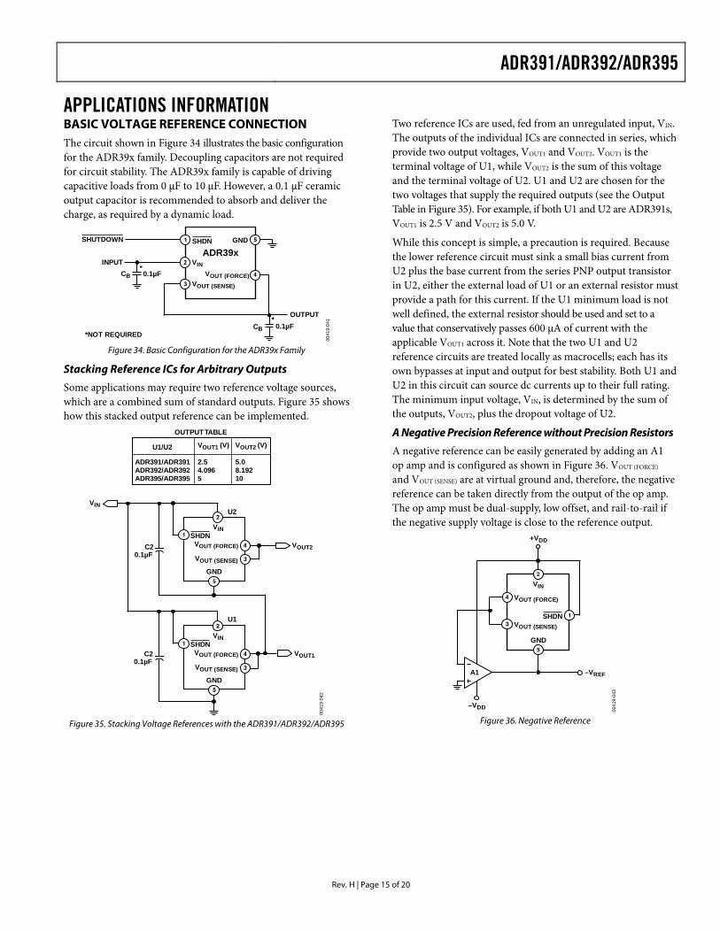
APPLICATIONS INFORMATION BASIC VOLTAGE REFERENCE CONNECTION The circuit shown in Figure 34 illustrates the basic configuration for the ADR39x family. Decoupling capacitors are not required for circuit stability. The ADR39x family is capable of driving capacitive loads from 0 μF to 10 μF. However, a 0.1 μF ceramic output capacitor is recommended to absorb and deliver the charge, as required by a dynamic load.
SHUTDOWN
INPUTCB 0.1µF
CB 0.1µF
*
*OUTPUT
*NOT REQUIRED
ADR39xSHDN GND
VOUT (SENSE)
VINVOUT (FORCE)
0041
9-04
1
Figure 34. Basic Configuration for the ADR39x Family
Stacking Reference ICs for Arbitrary Outputs
Some applications may require two reference voltage sources, which are a combined sum of standard outputs. Figure 35 shows how this stacked output reference can be implemented.
GND
U2
U1
C20.1µF
C20.1µF
OUTPUTTABLE
U1/U2
SHDN
VOUT (SENSE)
VOUT (FORCE)
VIN
VOUT1
VOUT2
VIN
VOUT1 (V) VOUT2 (V)
ADR391/ADR391ADR392/ADR392ADR395/ADR395
2.54.0965
5.08.19210
0041
9-04
2
GND
SHDN
VOUT (SENSE)
VOUT (FORCE)
VIN
Figure 35. Stacking Voltage References with the ADR391/ADR392/ADR395
Two reference ICs are used, fed from an unregulated input, VIN. The outputs of the individual ICs are connected in series, which provide two output voltages, VOUT1 and VOUT2. VOUT1 is the terminal voltage of U1, while VOUT2 is the sum of this voltage and the terminal voltage of U2. U1 and U2 are chosen for the two voltages that supply the required outputs (see the Output Table in Figure 35). For example, if both U1 and U2 are ADR391s, VOUT1 is 2.5 V and VOUT2 is 5.0 V.
While this concept is simple, a precaution is required. Because the lower reference circuit must sink a small bias current from U2 plus the base current from the series PNP output transistor in U2, either the external load of U1 or an external resistor must provide a path for this current. If the U1 minimum load is not well defined, the external resistor should be used and set to a value that conservatively passes 600 μA of current with the applicable VOUT1 across it. Note that the two U1 and U2 reference circuits are treated locally as macrocells; each has its own bypasses at input and output for best stability. Both U1 and U2 in this circuit can source dc currents up to their full rating. The minimum input voltage, VIN, is determined by the sum of the outputs, VOUT2, plus the dropout voltage of U2.
A Negative Precision Reference without Precision Resistors
A negative reference can be easily generated by adding an A1 op amp and is configured as shown in Figure 36. VOUT (FORCE) and VOUT (SENSE) are at virtual ground and, therefore, the negative reference can be taken directly from the output of the op amp. The op amp must be dual-supply, low offset, and rail-to-rail if the negative supply voltage is close to the reference output.
GND
A1
SHDN
+VDD
VOUT (FORCE)
VOUT (SENSE)
–VDD
VIN
–VREF
0041
9-04
3
Figure 36. Negative Reference
ADR391/ADR392/ADR395
Rev. H | Page 16 of 20
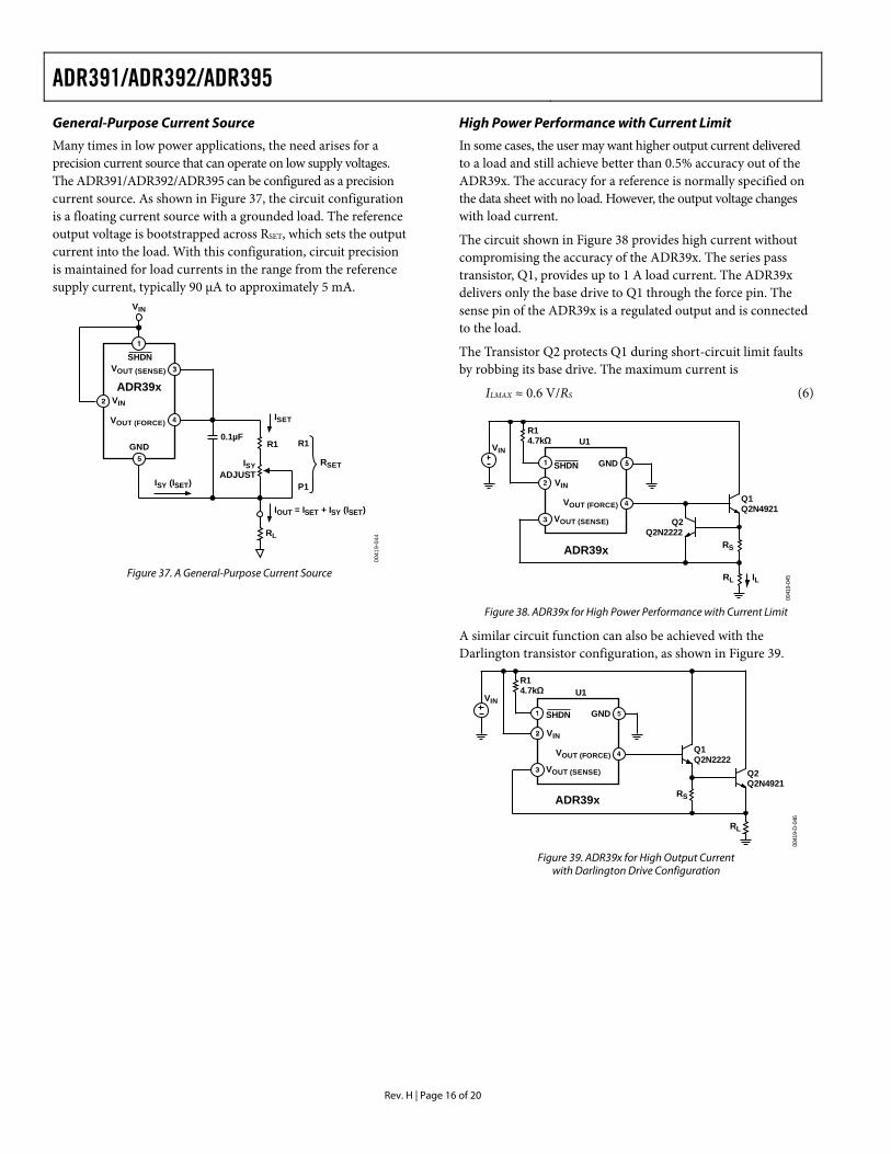
General-Purpose Current Source
Many times in low power applications, the need arises for a precision current source that can operate on low supply voltages. The ADR391/ADR392/ADR395 can be configured as a precision current source. As shown in Figure 37, the circuit configuration is a floating current source with a grounded load. The reference output voltage is bootstrapped across RSET, which sets the output current into the load. With this configuration, circuit precision is maintained for load currents in the range from the reference supply current, typically 90 μA to approximately 5 mA.
ADR39x
GND R1
P1
R10.1µF
SHDN
VIN
VIN
VOUT (FORCE)
VOUT (SENSE)
ISET
RSET
IOUT = ISET + ISY (ISET)
RL
ISYADJUST
ISY (ISET)
0041
9-04
4
Figure 37. A General-Purpose Current Source
High Power Performance with Current Limit
In some cases, the user may want higher output current delivered to a load and still achieve better than 0.5% accuracy out of the ADR39x. The accuracy for a reference is normally specified on the data sheet with no load. However, the output voltage changes with load current.
The circuit shown in Figure 38 provides high current without compromising the accuracy of the ADR39x. The series pass transistor, Q1, provides up to 1 A load current. The ADR39x delivers only the base drive to Q1 through the force pin. The sense pin of the ADR39x is a regulated output and is connected to the load.
The Transistor Q2 protects Q1 during short-circuit limit faults by robbing its base drive. The maximum current is
ILMAX ≈ 0.6 V/RS (6)
SHDN GND
U1
ADR39x
0041
9-04
5
VIN
VIN
VOUT (FORCE)
RL IL
RS
VOUT (SENSE) Q2Q2N2222
R14.7kΩ
Q1Q2N4921
Figure 38. ADR39x for High Power Performance with Current Limit
A similar circuit function can also be achieved with the Darlington transistor configuration, as shown in Figure 39.
ADR39x
GND
U1
0041
9-D
-046
SHDN
VIN
VIN
VOUT (FORCE)
RL
RS
VOUT (SENSE)
Q1Q2N2222
R14.7kΩ
Q2Q2N4921
Figure 39. ADR39x for High Output Current
with Darlington Drive Configuration
ADR391/ADR392/ADR395
Rev. H | Page 17 of 20
–150
DR
IFT
(ppm
)
150
TIME (Hours)0
–100
–50
0
50
100
100 200 300 400 500 600 700 1000
0041
9-00
2
900800
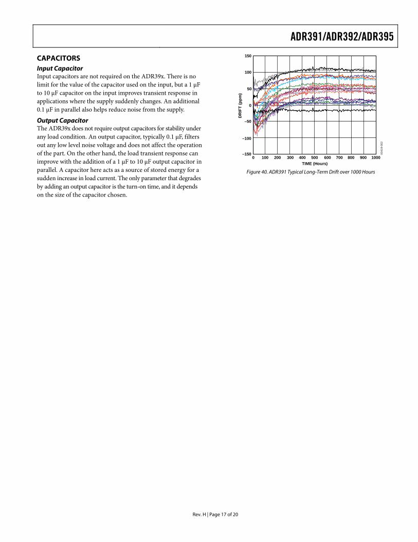
CAPACITORS Input Capacitor Input capacitors are not required on the ADR39x. There is no limit for the value of the capacitor used on the input, but a 1 μF to 10 μF capacitor on the input improves transient response in applications where the supply suddenly changes. An additional 0.1 μF in parallel also helps reduce noise from the supply.
Output Capacitor The ADR39x does not require output capacitors for stability under any load condition. An output capacitor, typically 0.1 μF, filters out any low level noise voltage and does not affect the operation of the part. On the other hand, the load transient response can improve with the addition of a 1 μF to 10 μF output capacitor in parallel. A capacitor here acts as a source of stored energy for a sudden increase in load current. The only parameter that degrades by adding an output capacitor is the turn-on time, and it depends on the size of the capacitor chosen.
Figure 40. ADR391 Typical Long-Term Drift over 1000 Hours
ADR391/ADR392/ADR395
Rev. H | Page 18 of 20
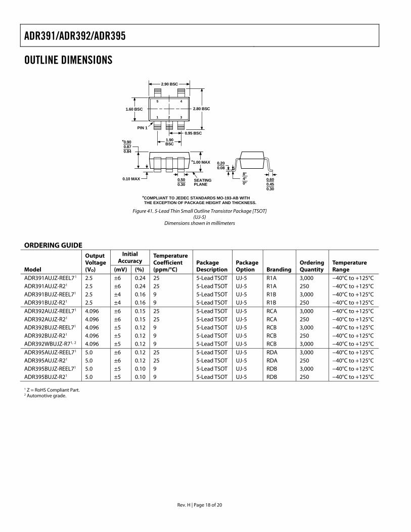
OUTLINE DIMENSIONS
*COMPLIANT TO JEDEC STANDARDS MO-193-AB WITHTHE EXCEPTION OF PACKAGE HEIGHT AND THICKNESS.
PIN 1
1.60 BSC 2.80 BSC
1.90BSC
0.95 BSC
0.200.08
0.600.450.30
8°4°0°
0.500.30
0.10 MAX SEATINGPLANE
*1.00 MAX
*0.900.870.84
2.90 BSC
5 4
1 2 3
Figure 41. 5-Lead Thin Small Outline Transistor Package [TSOT]
(UJ-5) Dimensions shown in millimeters
ORDERING GUIDE
Model
Output Voltage (VO)
Initial Accuracy
TemperatureCoefficient (ppm/°C)
Package Description
PackageOption Branding
Ordering Quantity
Temperature Range (mV) (%)
ADR391AUJZ-REEL71 2.5 ±6 0.24 25 5-Lead TSOT UJ-5 R1A 3,000 −40°C to +125°C ADR391AUJZ-R21 2.5 ±6 0.24 25 5-Lead TSOT UJ-5 R1A 250 −40°C to +125°C ADR391BUJZ-REEL71 2.5 ±4 0.16 9 5-Lead TSOT UJ-5 R1B 3,000 −40°C to +125°C ADR391BUJZ-R21 2.5 ±4 0.16 9 5-Lead TSOT UJ-5 R1B 250 −40°C to +125°C ADR392AUJZ-REEL71 4.096 ±6 0.15 25 5-Lead TSOT UJ-5 RCA 3,000 −40°C to +125°C ADR392AUJZ-R21 4.096 ±6 0.15 25 5-Lead TSOT UJ-5 RCA 250 −40°C to +125°C ADR392BUJZ-REEL71 4.096 ±5 0.12 9 5-Lead TSOT UJ-5 RCB 3,000 −40°C to +125°C ADR392BUJZ-R21 4.096 ±5 0.12 9 5-Lead TSOT UJ-5 RCB 250 −40°C to +125°C ADR392WBUJZ-R71, 2 4.096 ±5 0.12 9 5-Lead TSOT UJ-5 RCB 3,000 −40°C to +125°C ADR395AUJZ-REEL71 5.0 ±6 0.12 25 5-Lead TSOT UJ-5 RDA 3,000 −40°C to +125°C ADR395AUJZ-R21 5.0 ±6 0.12 25 5-Lead TSOT UJ-5 RDA 250 −40°C to +125°C ADR395BUJZ-REEL71 5.0 ±5 0.10 9 5-Lead TSOT UJ-5 RDB 3,000 −40°C to +125°C ADR395BUJZ-R21 5.0 ±5 0.10 9 5-Lead TSOT UJ-5 RDB 250 −40°C to +125°C 1 Z = RoHS Compliant Part. 2 Automotive grade.
ADR391/ADR392/ADR395
Rev. H | Page 19 of 20
NOTES
ADR391/ADR392/ADR395
Rev. H | Page 20 of 20
NOTES
©2002–2009 Analog Devices, Inc. All rights reserved. Trademarks and registered trademarks are the property of their respective owners. D00419-0-10/09(H)