microprocessor alu, control unit group of registers
TRANSCRIPT

1www.maduracoaching.com
MICROPROCESSOR
MICROPROCESSOR
A Microprocessor is a semiconductor device which is manufactured by using LSI
or VLSI technology, which includes ALU, Control Unit and a group of Registers
in a single Integrated circuit.
Micro controller: It is a device that includes microprocessor, memory, and I/O
signal lines on a single chip, fabricated using VLSI or ULSI technology.
Microcomputer: A digital computer having a microprocessor as its Central
Processing Unit is called Microcomputer. A microprocessor combined with
memory, an input device and an output device forms a microcomputer. Some
times microcontroller is called microcomputer.
Bit: Binary digit. (i.e., 0 or 1)
Nibble: A group of four bits is called a nibble.
Byte: A group of eight bits is called by byte.
Word: A group of bits the computer recognizes and processes at a time, 1 word =
2 byte.
Instruction: A command in binary that is recognized and executed by the
computer to accomplish a task.
Mnemonic Instruction: A meaningful combination of letters used to suggest the
operation of an instruction.
For ex. MOV, ADD, SUB etc.
Bus: A group of wires or lines used to transfer bits between the microprocessor
and other components of the computer system or path used to carry signals, such
as connection between memory and the CPU in a digital computer.
A MICROPROCESSOR AS A PROGRAMMABLE DEVICE
Microprocessor: The programmable means it can be instructed to perform given
tasks within its capability; Ex. A Plano is a programmable machine.

2www.maduracoaching.com
Memory: Memory is like the pages of a note book with space for a fixed number
of binary numbers on each line. However these pages are generally made of
semiconductor material. Typically, each line is an 8 bit register that can store
eight binary digits (bits) and several of these register are assigned in a sequence
called memory.
Input/output: The user can enter instructions and data into memory through
devices such as a keyboard or simple switches. These devices are called input
devices. The microprocessor reads the instruction from the memory and process
the data according to these instructions. The result can be displayed by a device
such as seven-segment LEDS (light emitting diodes) or printed by a printer, such
devices are called output devices.
Microprocessor as a CPU: The computer is represented in block diagram as
shown below. The block diagram shows that the computer has four component.
Memory, Input, output and the central processing unit, which consists of the
arithmetic/logic unit (ALU) and control unit. The CPU contains varying registers
to store data. The ALU performs arithmetic and logical operation by using
instruction from decoders, counters and control lines. The CPU reads
instructions from the memory and communicating with devices such as memory,

3www.maduracoaching.com
Input, and output. The timing of the communication process is controlled by the
group of circuits called the control unit.
Organization of a Microprocessor-Based System
The above given figure shows a simplified but formal structure of a
microprocessor based system. It includes four components; Microprocessor,
input, output and memory around a common communication path called a BUS.
The Microprocessor can be divided into 3 segments for the sake of clarity:
Arithmetic Logical Unit (ALU), register array and control unit.
(i) ALU: This is the area of the Microprocessor where various computing
functions are performed on data. The ALU unit performs such arithmetic
operation as addition and subtraction and such logic operations as AND,
OR and EX-OR; results are stored either in register or memory.
(ii) Register array: These registers are primarily used to store data
temporarily during the execution of a program.
(iii) Control unit: The control unit provides the necessary timing and controls
the flow of data between the microprocessor memory and peripherals.
Low Level Language: A medium of communication that is machine dependent
or specific to a given computer. The machine and the assembly languages of a
computer are considered low-level language.
High Level Language: A medium of communication that is independent of a
given computer programs are written in English like words and they can be
executed on machine using a translator (a compiler or an interpreter).

4www.maduracoaching.com
Complier: A program that translates english-like words of a high-level language
in the machine language of a computer.
Monitor Program: A program that interprets the input from a keyboard and
converts the input into its binary equivalent.
Microprocessor Architecture and Micro Computer System: A Microprocessor
system consists of four components: The Microprocessor, memory, input, and
output.
The Microprocessor manipulates data and communicates with such peripheral
devices such peripheral devices such as memory and I/O. The internal logic
design of the microprocessor is called its architecture.
Architecture: The process of data manipulation and communication is
determined by the logic design of the microprocessor, called the architecture. The
various function performed by the microprocessor can be classified in three
general categories:
(1) Microprocessor initiated operations.
(2) Internal data operations
(3) Peripheral (Externally) initiated operations.
To perform these functions, the 𝜇P requires a group of logic circuits and a set of
signals called control signals. The Microprocessor functions listed above are
explained here in relation to the 8085 or 8080(A).
The MPU performs primarily
1. Memory read: Reads data from memory.
2. Memory write: Writes data into memory.
3. I/O read: Accepts data from input devices.
4. I/O write: Sends data to output devices.
The MPU needs to perform the following steps:
5www.maduracoaching.com
Input: The input section transfers data and instructions in binary from the
outside world to the microprocessor. It includes such devices as a keyboard a
teletype and analog to digital converter.
Output: The output section transfers data from the microprocessor to such
output devices as light emitting diodes (LEDs), a cathode ray tube (CRT), a
printer, a magnetic tape or another computer.
Memory: Memory stores such binary information as instructions and provides
that information to the microprocessor whenever necessary, Memory has two
sections Read only Memory (ROM) and Read/Write memory (R/WM) popularly
known as random access memory (RAM).
ROM: The ROM restore programs that do not need alterations. The monitor
program of a single board Microcomputer is generally stored in the ROM.
Programs stored in the ROM can only be read they can altered.
Read/Write memory: R/W memory is also known as user memory it is used to
store user programs and data. The information stored in this memory can be
easily read and altered.
System bus: The system bus is a communication path between the
microprocessor and peripheral. It is nothing but a group of wires to carry bits.
The Microprocessor communicates with only one peripheral at a time, but here
one important question arises. How does the Microprocessor work? The program
includes binary instructions to add given data and display the answer at the
seven segment display i.e., LEDs. When the 𝜇P is given a command to execute
the program, it reads and executes one instruction at a time and finally since the
result to the seven segment LEDs to display.
Microprocessor-Initiated operations and 8085 BUS organization:
The MPU performs primarily four operations:
1. Memory Read: Reads data from memory.
2. Memory Write: Writes data into memory.

6www.maduracoaching.com
3. I/O Read: Accepts data from input devices.
4. I/O Write: Sends data to output devices.
The MPU needs to perform the following steps.
Step 1: Identify the peripheral or the memory location
Step 2: Transfer data
Step 3: Provide timing or synchronization signals.
The 8085 MPU performs these functions using three sets of communication lines
called buses, namely-address bus, data bus and the control bus.
Address bus: The address bus is a group of 16 lines generally identified as 𝐴0to
𝐴15 . The address bus is unidirectional bits flow in the one direction from the
MPU to peripheral device. In a computer system, each peripheral or memory
location identified by a binary number called an address and the address bus is
used to carry a 16-bit address.
Data bus: The data bus is a group of eight lines used from data flow. These lines
are bidirectional i.e., data flow in both directions between the MPU & peripheral
devices. The largest number that can appear on the data bus is 1111 1111 (25510).
It determines the work length and the register size of a microprocessor, thus the
8085 𝜇p is called an 8-bit 𝜇p. Microprocessors such as Intel 8086. Zilog Z8000,
and Motorola 6800 have 16 data lines, they are known as 16-bit Microprocessors.

7www.maduracoaching.com
Control bus: The control bus is comprised of various single lines that carry
synchronization signals. The MPU uses such lines to perform the third functions
of providing timing signals. Control bus is mixed direction i.e., some lines into
𝜇p and some others out of 𝜋𝑝.
Internal data operations and the 8085 register: The internal architecture of 8085
microprocessor determines how and what operations must be performed with
the data. These operations are:
1. Store 8-bit data
2. Perform arithmetic and logical operations
3. Test for conditions
4. Sequence the execution of instructions
5. Store the data temporarily during execution in the defined R/Q memory
location called the stack. Fig. shown below is a simplified representation of
the 8085 internal architecture of register.
Accumulator: The Accumulator is an 8-bit register that is part of the ALU. This
register is used to store 8-bit data and to perform Arithmetic and Logical
operations. The result of an operation is stored in accumulator.
Flags: The ALU includes 5 flip-flops that are set or reset according to data
conditions in the accumulator. For Ex: After an addition of two number if the
sum in the accumulator is larger than eight bits, the flip-flop that is used to
indicate a carry called the carry flag (CY) becomes set.

8www.maduracoaching.com
Program Counter (PC): Is a 16-bit register used to hold memory addresses. The
size of this register is 16 bits because the memory addresses are 16 bits. Program
counter is used to sequence execution of a program. It always holds the address
of the next memory location to be accessed.
It keeps the track of memory addresses of the instructions in a program while
they are being executed.
Stack pointer: The stack pointer is also a 16-bit register. Basically stack is a group
of memory locations in the R/W memory that is used for temporary storage of
binary information during the execution of a program.
Stack pointer works on the principle of LIFO (Last-in-first-out)
The stack pointer holds the address of the top element of data stored in the stack.
The stack pointer is initialized by the programmer at the beginning of a program
which needs stack operation.
Stack Pointer (SP) stores the contents of Program Counter (PC) when ti jumps to
a subroutine using CALL instruction.
Sometimes stack memory is called rough memory.
The stack is shared by the programmer and the microprocessor.
The beginning of the stack is defined in the program by using the instruction LXI
SP or SPHL.
The programmer can store and retrieve the contents of a register pair by using
PUSH and POP instructions.
Some commonly used components are given below.
Tri-State devices: Tri state logic devices have three stages; logic 1, logic 0 and
high impedance. A tri-state logic devices has a third line called enable, as shown
below in figure.
Fig. (1)a shows a tri-state inverter. When the enable is high this circuit functions
as an ordinary inverter, when the enable is low; the inverter stays in the high
impedance state. Fig. 1(b) also shows a tri state inverter with active low Enable
line.

9www.maduracoaching.com
Buffer: Buffer has three logic states namely 0, 1 and high impedance (Z).
Basically buffer is used to transfer the data. The active buffer is a logic circuit that
amplifies the current or power. It has one input line and one output line as
shown in Fig. 2(a). The logic level of the output is the same as that of the input.
Logic 1 input provides logic one output. Fig. 2(b) also shown a tristate buffer
when the enable line is low, the circuit functions as a buffer, otherwise it stays in
the high impedance state.
DECODER: The decoder is a logic circuit that identifies each combination of the
signals present at its input.
For example: If the input to a decoder has two binary lines, the decoder will have
four output lines. i.e., 2 × 4 line decoder.
ENCODER: The encoder is a logic circuit that provides the appropriate code;
binary, BCD etc. as output for each input signal. This process is reverse of
decoding.
8085 MICROPROCESSOR ARCHITECTURE:
The 8085 is an 8-bit general purpose microprocessor capable of addressing 64 K
of memory. The device has 40 pins, requires a + 5 V single power supply and can
operate with a 3 MHz single phase clock. Fig. given below shows the logic pin out of the
8085 𝜇P, All the signals can be classified in to six groups (1) address bus, (2) data bus,

10www.maduracoaching.com
(3) control signals, (4) power supply and frequency signals, (5) externally initiated
signals and (6) serial input-output ports.
Pin Diagram of 8085
Control and status signals: This group of signals includes two control signals
(𝑅𝐷 𝑎𝑛𝑑 𝑊𝑅 ). Three status signals (IO/M, 𝑆1 and 𝑆0) and ALE.
ALE: This signals is used primarily to latch the low-order address from the multiplexed
data bus and generate a separate set of eight address lines, 𝐴7 − 𝐴0.
𝑹𝑫 : Read: This is a Read control signal. This signal indicates that the selected I/O or
memory device is to be read and data are available on the data bus.
𝑾𝑹 : Write: This is write control signal. This signal indicates that the data one the data
bus are to be written in to a selected memory or I/O and memory operation. When it is
low, it indicates a memory operation.
IO/𝑴 : This is a status signal used to differentiate between I/O and memory operation.
When it is low, it indicates a memory operation.
𝑺𝟏 𝒂𝒏𝒅 𝑺𝟎: These status signals similar to IO/𝑀 can identify various operations.

11www.maduracoaching.com
8085 Interrupts and Externally Initiated Signals
INTR (Input) Interrupts Request: This is used as a general purpose.
INT A (OUTPUT):Interrupt acknowledge: This is used to acknowledge and
interrupt.
RST 7.5
RST 6.5
RST 5.5
Restart Interrupts: These are vectored interrupts and transfer the program
control to specific memory locations. They cause an internal restart to be
automatically inserted. They have higher priorities than INTR interrupt. Among
these three, the priority order is 7.5, 6.5, 5.5.
8085 have five hardware interrupts: TRAP (Highest priority) RST 7.5, RST 6.5,
RST 5.5 and INTR (Lowest priority).
RST 7.5 is positive edge triggered while RST 6.5 and RST 5.5 is level triggered
interrupt.
TRAP is both edge and level triggered interrupt.
Except TRAP all other interrupts are called maskable Interrupts.
TRAP (INPUT): This is a non-maskable interrupt and the highest priority
and INTR is least priority.
Non-maskable means we cannot disable this interrupt.
HLDA: HOLD Acknowledge. This signal acknowledges the hold request.
HOLD: (Input): This signal indicates that a peripheral such as a DMA controller
is requesting the use of the address and data BUS.
Ready (Input): This signal is used to delay the microprocessor read or write
cycles with a slow responding peripheral is ready to send or accept data, when
this signal goes low. The microprocessor waits for an integral number of clock
cycles until it goes high.
12www.maduracoaching.com
ALU: The arithmetic / logic circuit performs the computing functions, includes
the accumulator, the temporary register, the arithmetic and logic circuits and five
flags. The result is stored in accumulator.
Register Array: These registers are used to hold 8-bit data during the execution
of some instructions.
NOTE:
(1) In the memory write cycle, the 8085 writes (stores) data in memory using the
control signal and the status signal IO/𝑀 .
(2) In the memory read cycle, the 8085 asserts the 𝑅𝐷 signal to memory and than
8085 places the data byte on the data bus and then asserts the 𝑊𝑅 signal to
write into the addressed memory.
POINTS TO RMEMBER:
(1) The data bus and the low order address bus are multiplexed; they can be
demultiplexed by using the ALE (Address Latch Enable) signal and a latch.
(2) The IO/𝑀 is a status signal. When it is high, it indicates an I/𝑂 operation.
When it is low, it indicates a memory operation.
(3) The 𝑅𝐷 𝑎𝑛𝑑 𝑊𝑅 are control signals. The 𝑅𝐷 is asserted to read from an
external device and the 𝑊𝑅 is asserted to write into an external device.
(4) The 𝑅𝐷 and 𝑊𝑅 signal are logically ANDed with IO/M signal to generate
four active low control signals; 𝑀𝐸𝑀𝑅 , 𝑀𝐸𝑀𝑊 , 𝐼𝑂𝑅 𝑎𝑛𝑑 𝐼𝑂𝑊 .
(5) Each instruction of the 8085 𝜇P can be divided into a few basic operations,
called machine cycles and each machine cycle can be divided in to T – States.
(6) The frequently used machine cycles are Opcode fetch, Memory Read,
Memory Write, I/O Read and I/O write.
(7) The opcode fetch and the memory read are operationally similar. The 8085
reads opcode during the opcode fetch cycle, and it reads 8-bit data during the
memory read cycle.

13www.maduracoaching.com
(8) To interface a memory chip with the 8085, it is necessary that low order
address lines of the 8085 address bus are connected to the address lines of the
memory chip. The higher order address lines are decoded to generate 𝐶𝑆
signal to enable the chip.
Based on the operation performed by each instruction, the 8085 instructions can
be classified into five groups namely:
(i) Data transfer instruction
(ii) Arithmetic instruction
(iii) Logical instruction
(iv) Branch instruction
(v) Machine control, stack and I/O related instructions.
An instruction is a command to the microprocessor to perform a given task on
specified data.
Each instruction has two parts:
(i) Operation code (OP-code): It specifies the task to be performed by
computer.
(ii) Operand: it specifies the data to be operated.
For example:
(i) MOV C.A
(ii) ADD B
(iii) CMA
In (i) part OP-code is MOV and operand is C, A
In (ii) part OP-code is ADD and operand is B
In (iii) part OP-code is CMA and no operand.
The meaning of the first part is, copy the contents of the accumulator in
register C.

14www.maduracoaching.com
The meaning of the second part is, add the contents of the register B to the
contents of the accumulator and store the result in the accumulator.
The meaning of third part is to invert (complement) each bit in the
accumulator.
The operand (data) given in the instruction may be in various forms such as 8-bit
or 16-bit address, internal registers or a register or memory location. In some
instructions the operand is implicit (not expressed in a direct way).
When operand is register, it is understood that the data is the content of the
register.
The time required to complete the operation of accessing either memory or I/O,
is called machine cycle. One machine cycle consists of 3T to 6T-states.
T-states means the operation performed in one clock period. (In 8085 T-state
value = 1/3 𝜇𝑆).
The time required to complete the execution of an instruction, is called
instruction cycle.
Instruction cycle = Fetch cycle + Execute cycle.
The 8085 instruction cycle consists of 1 to 5 machine cycle or 1 to 5 operations.
The 1st Machine cycle of 8085 consists of 4T to 6T-states and all other subsequent
machine cycles consist of 3T-states only.
The First machine cycle of each instruction cycle is always OP-code fetch
machine cycle. Other machine cycles are Memory read and Memory write.
In 8085, CALL instruction is the lengthy instruction which takes 18T states and
the shortest instruction takes only 4T states. (Ex. MOV A, B).
Example of Arithmetic Instructions: ADD, SUB, ADI, SUI, ADC, SBB, ADI, SBI,
INR, DCR, INX, DCX etc.
Example of Data Transfer Instructions: LDA, STA, MOV, MVI etc.
Example of Logical Instructions: ORA, ANA, XRA, ORI, ANI, XRI, RLC, RRC,
RAL etc.
Example of Branch Instructions: JMP, CALL, RC, RNC, JC, JNC, CC, CNC etc.
15www.maduracoaching.com
Example of Stack, I/O and Machine control Instruction: IN, OUT, PUSH, POP,
HLT, NOP, SIM, RIM etc.
According to the length of instruction, the 8085 instructions can be classified into
three groups:
(i) One byte Instructions: This type of Instruction requires one memory
location to store in memory. The one byte instructions include both
opcode and operand in the same byte, e.g., MOV A, B. ADD B, CMA etc.
(ii) Two byte instructions: This type of instruction requires two memory
locations to store in memory. In a two byte instruction, the first byte
specifies the operation code and the second byte specifies the operand,
e.g., MVI A, 45 H; ADI 36 H, SUI 78 H, ORI 67 H, XRI 9A H etc.
(iii) Three byte instructions: This type o instruction requires three memory
location to store in the memory. In three byte instruction, the first byte
specifies the Opcode and the following two bytes specify the 16-bit
address or data.
Ex.: JMP 2500 H, STA 4509 H, LDA 3456 H, LXI, 2345 H etc.
NOTE:
1. One-Byte Instructions can be recognized as follows:
(a) Data transfer instructions that copy the contents from one register (or
memory) into another register (or memory) are one-byte instruction.
Ex. MOV.
(b) Arithmetic / logical instructions without the ending letter ‘I’ are one byte.
Ex. ADD, SUB, ORA.
2. Two byte instructions can be recognized as follows:
(a) Instructions that load or manipulate 8-bit data directly, are 2-byte
instructions.
Ex. MVI, ADI, SUI, SBI, IN, OUT, ORI, XRI, ANI etc.
16www.maduracoaching.com
(b) All three letter instructions with ending letter ‘I’ (except LXI) are two byte
instructions.
3. Three-Byte instructions can be recognized as follows:
The Instructions that load 16 bits are referred to memory addresses are 3-byte
instructions.
Ex. LXI, JMP, conditional jumps, CALL, conditional calls, STA, LDA, LHLD,
SHLD.
Addressing modes: The way in which the operand information is specified in the
instruction code, is called addressing mode. The 8085 microprocessor supports,
five addressing modes.
1. Implicit or Inherent addressing mode: There are certain instructions which
operate on the content of the accumulator. Such instructions do not require
the address of the operand.
Ex. CMA, STC, RLC, RRC, RAL, RAR etc.
2. Direct addressing mode: In this mode, the address of the operand (data) is
given in the instruction itself.
Ex.STA, LDA, SHLD, LHLD, IN, OUT etc.
3. Register addressing mode or (register direct):In this mode, the operands are
in the general purpose registers. The operation code specifies the address of
the register in addition to the operation to be performed.
Ex. MOV A, B; ADDB; SUB C; ORA B; etc.
4. Register Indirect addressing mode: In this mode, the address of the operand
is specified by a register pair,
Ex. STAX, LDAX etc.
5. Immediate addressing mode: In this mode, the operand is specified in the
instruction itself.
Ex. MVI, ADI, LXI, ORI, SUI, SBI, ACI, XRI, ANI etc.
Note: All the branch operations use immediate addressing modes.

17www.maduracoaching.com
In some instruction only resistor is specified. The content of the specified register
is one of the operands. It is understood that the other operand is in accumulator.
The operation of CALL and RET instructions are similar to that of the operation o
PUSH and POP instructions.
IO/𝑀 , 𝑆0, 𝑆1 are status signals and 𝑅𝐷 , 𝑊𝑅 are the control signals available in
8085.
IO/𝑴 : It is a status signal used to differentiate between I/O operation and
memory operation. When it is low, it indicates memory operation. This signal is
combined with RD (read) and WR (write) to generate I/O and memory control
signals.
IO/𝑴 𝑹𝑫 𝑾𝑹 Operation
0 0 1 Memory read operation
0 1 0 Memory write operation
1 0 1 I/O read operation
1 1 0 I/O write operation
S1 and S0: These are status signals sent by the microprocessor to distinguish the
various types of operations as given below:
S1 S0 Operation
0 0 HALT
0 1 WRITE
1 0 READ
1 1 FETCH
Comparison of PUSH and POP instructions:
The instructions PUSH and POP are similar to the instructions CALL and
RETURN respectively. The similarities and differences are as follows:
PUSH and POP
1. The programmer used the instructions PUSH to save the contents of register
specified in the register pair on the stack.

18www.maduracoaching.com
2. When PUSH is executed, the stack pointer register is decremented by two.
3. The instruction POP transfers the contents of the top two locations of the
stack to the specified register pair.
4. When the instruction POP is executed the stack pointer is incremented by
two.
5. There are no; conditional PUSH and POP instructions.
CALL and RETURN
1. When CALL is executed, the microprocessor automatically stores the 16-bit
address of the instruction next to CALL on the stack.
2. When CALL is executed, the stack pointer register is decremented by two.
3. Two instruction RET transfers the contents of the top two locations of the
stack to program counter.
4. When the instruction RET is executed, the stack pointer is incremented by
two.
5. In addition to the unconditional CALL and RET instructions, there are eight
conditional CALL and RETURN instructions.
Mapping: Assigning addresses to I/O devices or memory locations, is called
mapping.
Memory mapping: Assigning address to memory locations, is called memory
mapping.
(i) Changing the hardware logic used for the chip selection can change
memory mapping.
(ii) To interface a memory chip with the 8085, the necessary low-order
address lines of the 8085 address bus are connected to the address line of
the memory chip.
(iii) The high-order address lines are decoded to generate CS (chip select
signal to enable the chip).

19www.maduracoaching.com
Absolute decoding: In this decoding all the address lines which are not used for
memory chip to identify a memory register must be decoded. Thus, chip select
can be asserted by only one address.
Linear decoding: In this decoding technique, one address line is used for CS,
and others are left don’t care. This technique reduces hardware, but generates
multiple addresses resulting in fold back memory space.
I/O devices can be connected to microprocessor in two different techniques.
(i) Memory mapped I/O technique and
(ii) I/O mapped or Peripheral mapped I/O technique.
(i) Memory mapped I/O technique:
In memory mapped I/O, the I/O devices are also treated as memory
locations, under that assumption they will be given 16-bit address.
In memory mapped I/O, microprocessor uses memory related instructions
to communicate with I/O devices.
Ex.: STA, LDA, MOV A, M; MOV M, A etc.
In memory mapped I/O, MEMR and MEMW control signals are used to
activate I/O devices.
In memory mapped I/O, the entire memory map is shared by memory
locations and I/O devices. One address can be used only once. This
technique is used in a system where the number of I/O devices are more.
The maximum number of I/O devices that can connected to
microprocessor in this technique are 65536.
(ii) I/O mapped I/O technique:
In this technique the I/O devices are identified by the microprocessor with
separate 8-bit port address.
This technique uses separate control signals (IOR and IOW) to activate I/O
devices and separate instructions (IN and OUT) to communicate with I/O
devices.

20www.maduracoaching.com
In this technique I/O mapping is independent of memory mapping. Same
address can be used to identify input and output devices.
This technique is used in a system where number of I/O devices are less.
By using this method a maximum of 256 input devices and 256 output
devices can be connected to the processor (total of 512 I/O devices).
Interfacing: Designing hardware circuit and writing software instructions to
enable the microprocessor to communicate with peripheral devices, is called
interfacing. And the hardware circuit is called the interfacing device.
There are two basic types of interfacing devices available.
(i) Non-programmable interfacing devices and
(ii) Programmable interfacing devices.
(i) Non-programmable interfacing devices: Once the microprocessor based system
is designed, it is not possible to program such type of devices. Examples: 8212-
Non-programmable I/O part. 74LS245-bi-directional buffers, 74LS373
transparent latches etc.
(ii) Programmable interfacing devices: Writing a specific word, called the control
word, according to the internal logic, can program a programmable interfacing
device.
8155: Programmable peripheral interfacing (PPI) device with 256 bytes
RAM and 16-bit timer/counter. It is a general purpose interfacing device
i.e., it can be used to interface variety of I/O devices to the
microprocessor.
8255: PPI is also called programmable Interface Adapter (PIA). It consists
of three 8-bit ports.
THE 8085 FLAGS
Flags: The flags are affected by the arithmetic and logic operations in the ALU.
The flags generally reflect data conditions in the accumulator. The descriptions
and conditions of the flags are as follows.

21www.maduracoaching.com
X = denotes the Flags which are not in use.
S (Sign Flag): After the execution of an arithmetic or logic operation if the result
is one, the sign flag is set. This flag is used with sign numbers. If bit D7 is 1, the
number will be viewed as a negative number, if it is 0, the number will be
considered positive.
This bit is irrelevant for the operations of unsigned numbers. Therefore, for
unsigned number even if bit D7 of a result is 1 and the flag is set, it does not
mean the result is negative.
Z (Zero flag): The zero flag is set if the ALU operation results in zero, and the
flag is reset if the result is not zero.
AC (Auxiliary carry flag): In an arithmetic operation, when a carry is generated
by digit D3 and place on to digit D4, the AC flag is set.
AC flag is used internally for BCD arithmetic; the instruction set does not
include any conditional jump instructions based on the AC flag.
P (Parity flag): After an arithmetic or logical operation if the result has an even
number of ones, the flag is set. It is has an odd number of ones, the flag is reset.
CY (Carry flag): If an arithmetic operation results in a carry, the carry flag is set,
otherwise it is reset.
Meaning of some different types of 8085 instructions:
(i) Logical Operations: These instructions perform various logical operations
with the contents of the accumulator.
AND, OR, Exclusive – OR: Any 8-bit number or the contents of a register of
a memory location can be logically ANDed, ORed or Exclusive ORed with
the contents of the accumulator. The results are stored in the accumulator.
22www.maduracoaching.com
Compare: Any 8-bit number, or the contents of a register or a memory
location can be compared for equality, less than, greater than with the
contents of accumulator.
CMA: Complement the contents of the accumulator, Here all 0’s replaced
by 1’s and all 1’s replaced by 0’s.
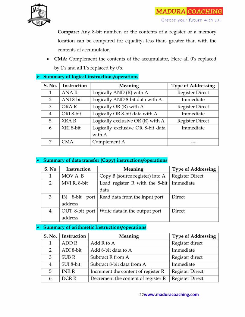
Summary of logical instructions/operations
S. No. Instruction Meaning Type of Addressing
1 ANA R Logically AND (R) with A Register Direct
2 ANI 8-bit Logically AND 8-bit data with A Immediate
3 ORA R Logically OR (R) with A Register Direct
4 ORI 8-bit Logically OR 8-bit data with A Immediate
5 XRA R Logically exclusive OR (R) with A Register Direct
6 XRI 8-bit Logically exclusive OR 8-bit data
with A
Immediate
7 CMA Complement A ---
Summary of data transfer (Copy) instructions/operations
S. No Instruction Meaning Type of Addressing
1 MOV A, B Copy B (source register) into A Register Direct
2 MVI R, 8-bit Load register R with the 8-bit
data
Immediate
3 IN 8-bit port
address
Read data from the input port Direct
4 OUT 8-bit port
address
Write data in the output port Direct
Summary of arithmetic Instructions/operations
S. No. Instruction Meaning Type of Addressing
1 ADD R Add R to A Register direct
2 ADI 8-bit Add 8-bit data to A Immediate
3 SUB R Subtract R from A Register direct
4 SUI 8-bit Subtract 8-bit data from A Immediate
5 INR R Increment the content of register R Register Direct
6 DCR R Decrement the content of register R Register Direct
23www.maduracoaching.com
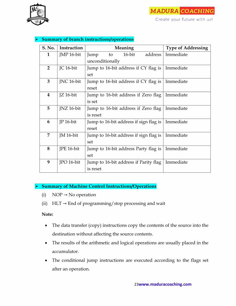
Summary of branch instructions/operations
S. No. Instruction Meaning Type of Addressing
1 JMP 16-bit Jump to 16-bit address
unconditionally
Immediate
2 JC 16-bit Jump to 16-bit address if CY flag is
set
Immediate
3 JNC 16-bit Jump to 16-bit address if CY flag is
reset
Immediate
4 JZ 16-bit Jump to 16-bit address if Zero flag
is set
Immediate
5 JNZ 16-bit Jump to 16-bit address if Zero flag
is reset
Immediate
6 JP 16-bit Jump to 16-bit address if sign flag is
reset
Immediate
7 JM 16-bit Jump to 16-bit address if sign flag is
set
Immediate
8 JPE 16-bit Jump to 16-bit address Party flag is
set
Immediate
9 JPO 16-bit Jump to 16-bit address if Parity flag
is reset
Immediate
Summary of Machine Control Instructions/Operations
(i) NOP → No operation
(ii) HLT → End of programming/stop processing and wait
Note:
The data transfer (copy) instructions copy the contents of the source into the
destination without affecting the source contents.
The results of the arithmetic and logical operations are usually placed in the
accumulator.
The conditional jump instructions are executed according to the flags set
after an operation.

24www.maduracoaching.com
Data transfer instructions do not set the flags.
The instruction ADD A will add the content of the accumulator to itself; this
is equivalent to multiplying by 2.
The instruction SUB A will subtract the content of the accumulator to itself;
this will clear the accumulator. The flag status will be CY = 0, Z = 1 always.
Registers are used to load data directly or to save data bytes.
The instructions JNR and DCR:
(i) Affect the contents of the specified register
(ii) Affect all the flags except the CY flag
The instruction CMA does not affect any flag.
The branch instructions are classified in three categories:
1. Jump instructions
2. Call and return instructions
3. Restart instructions
The jump instructions specify the memory location explicitly. Jump
instructions are three byte instructions.
Jump instructions are classified into two categories:
(i) Unconditional jump
(ii) Conditional jump
All the branch instructions use immediate addressing.
The call and return instructions are associated with the subroutine
technique.
Restart instructions are associated with the interrupt technique.
The conditional jump instructions check the flag conditions and make
decisions to change or not to change the sequence of a program.
Instruction CMP means compare with accumulator. Here the comparison is
performed by subtracting the contents of the operand (Register or Memory)
from the contents of accumulator.

25www.maduracoaching.com
(i) If A < (Register / Memory) → CY = 1, Z = 0
(i.e., carry flag set and zero flag reset)
(ii) If A = (Register / Memory) → Z = 1
(i.e., zero flag is set)
(iii) If A > (Register / Memory) → CY = 0 and Z = 0
(i.e., both the carry and zero flag reset)
Instruction CPI means compare immediate with accumulator.
(i) If A < Data → CY = 1, Z = 0
(ii) If A = Data → Z = 1, CY = 0
(iii) If A > Data → CY = 0, Z = 0
Note: Here both the contents are preserved and the comparison is shown by
setting the flags.
Some very important 8085 Instructions
RLC: Rotate Accumulator Left
𝑆𝑡𝑎𝑡𝑒𝑠 → 4 𝑀𝑎𝑐ℎ𝑖𝑛𝑒 𝑐𝑦𝑐𝑙𝑒𝑠 → 1 𝐴𝑑𝑑𝑟𝑒𝑠𝑠𝑖𝑛𝑔 𝑀𝑜𝑑𝑒 → 𝐼𝑚𝑝𝑙𝑖𝑐𝑖𝑡
RRC: Rotate Accumulator Right

26www.maduracoaching.com
𝑆𝑡𝑎𝑡𝑒𝑠 → 4 𝑀𝑎𝑐ℎ𝑖𝑛𝑒 𝑐𝑦𝑐𝑙𝑒𝑠 → 1 𝐴𝑑𝑑𝑟𝑒𝑠𝑠𝑖𝑛𝑔 𝑀𝑜𝑑𝑒 → 𝐼𝑚𝑝𝑙𝑖𝑐𝑖𝑡
RAL: Rotate Accumulator Left through carry
𝑆𝑡𝑎𝑡𝑒𝑠 → 4 𝑀𝑎𝑐ℎ𝑖𝑛𝑒 𝑐𝑦𝑐𝑙𝑒𝑠 → 1 𝐴𝑑𝑑𝑟𝑒𝑠𝑠𝑖𝑛𝑔 𝑀𝑜𝑑𝑒 → 𝐼𝑚𝑝𝑙𝑖𝑐𝑖𝑡
RAR: Rotate Accumulator Right through carry
𝑆𝑡𝑎𝑡𝑒𝑠 → 4 𝑀𝑎𝑐ℎ𝑖𝑛𝑒 𝑐𝑦𝑐𝑙𝑒𝑠 → 1 𝐴𝑑𝑑𝑟𝑒𝑠𝑠𝑖𝑛𝑔 𝑀𝑜𝑑𝑒 → 𝐼𝑚𝑝𝑙𝑖𝑐𝑖𝑡
Branch Instructions
S. No. Type of Instruction Machine Cycles T-states
1 Unconditional Jump
(Ex. JMP addr.)
3 10
2 Conditional Jump 2/3 (2 if condition is
not true and 3 if
condition is true)
7/10 (7 if condition is
not true and 10 if
condition is true)
3 Unconditional CALL 5 18
4 Conditional CALL 2/5 9/18

27www.maduracoaching.com
5 Conditional RETURN 1/3 6/12
RST: (Restart)
[SP – 1] ← [PCH]
[SP – 2] ← [PCL]
[SP] ← [SP – 2]
𝑆𝑡𝑎𝑡𝑒𝑠 → 12 𝑀𝑎𝑐ℎ𝑖𝑛𝑒 𝑐𝑦𝑐𝑙𝑒𝑠 → 3 𝐴𝑑𝑑𝑟𝑒𝑠𝑠𝑖𝑛𝑔 → 𝑅𝑒𝑔𝑖𝑠𝑡𝑒𝑟 𝐼𝑛𝑑𝑖𝑟𝑒𝑐𝑡
PCHL: Jump to address specified by H-L pair
[PC] ← [H – L]
[PCH] ← H
[PCL] ← L
𝑆𝑡𝑎𝑡𝑒𝑠 → 6 𝑀𝑎𝑐ℎ𝑖𝑛𝑒 𝑐𝑦𝑐𝑙𝑒𝑠 → 1 𝐴𝑑𝑑𝑟𝑒𝑠𝑠𝑖𝑛𝑔 → 𝑅𝑒𝑔𝑖𝑠𝑡𝑒𝑟
PUSH PSW: PUSH processor status word
[SP] – 1 ← A
[SP] – 2 ← PSW (Program Status Word)
[SP] ← [SP] – 2
𝑆𝑡𝑎𝑡𝑒𝑠 → 12 𝑀𝑎𝑐ℎ𝑖𝑛𝑒 𝑐𝑦𝑐𝑙𝑒𝑠 → 3
𝐴𝑑𝑑𝑟𝑒𝑠𝑠𝑖𝑛𝑔 → 𝑅𝑒𝑔𝑖𝑠𝑡𝑒𝑟 𝑆𝑜𝑢𝑟𝑐𝑒 /𝑅𝑒𝑔𝑖𝑠𝑡𝑒𝑟 𝐼𝑛𝑑𝑖𝑟𝑒𝑐𝑡 (𝑑𝑒𝑠𝑡𝑖𝑛𝑎𝑡𝑖𝑜𝑛)
POP PSW: POP Processor Status Word
[SP] + 1 ← A
[SP] + 2 ← PSW (Program Status Word)
[SP] ← [SP] + 2
𝑆𝑡𝑎𝑡𝑒𝑠 → 10 𝑀𝑎𝑐ℎ𝑖𝑛𝑒 𝑐𝑦𝑐𝑙𝑒𝑠 → 3 𝐴𝑑𝑑𝑟𝑒𝑠𝑠𝑖𝑛𝑔 → 𝑅𝑒𝑔𝑖𝑠𝑡𝑒𝑟 𝐼𝑛𝑑𝑖𝑟𝑒𝑐𝑡
XTHL: Exchange stack-top with H-L pair
[L] ← [SP]

28www.maduracoaching.com
[H] ← [SP] + 1
𝑆𝑡𝑎𝑡𝑒𝑠 → 16 𝑀𝑎𝑐ℎ𝑖𝑛𝑒 𝑐𝑦𝑐𝑙𝑒𝑠 → 5 𝐴𝑑𝑑𝑟𝑒𝑠𝑠𝑖𝑛𝑔 → 𝑅𝑒𝑔𝑖𝑠𝑡𝑒𝑟 𝐼𝑛𝑑𝑖𝑟𝑒𝑐𝑡
SPHL: Move the contents of H-L pair to stack pointer
[H – L] → [SP]
𝑆𝑡𝑎𝑡𝑒𝑠 → 6 𝑀𝑎𝑐ℎ𝑖𝑛𝑒 𝑐𝑦𝑐𝑙𝑒𝑠 → 1 𝐴𝑑𝑑𝑟𝑒𝑠𝑠𝑖𝑛𝑔 → 𝑅𝑒𝑔𝑖𝑠𝑡𝑒𝑟
Some Instructions which do not use any addressing
EI: Enable Interrupt
DI: Disable Interrupt
SIM: Set Interrupt Mask
RIM: Read Interrupt Mask
NOP: No Operation
𝑆𝑡𝑎𝑡𝑒𝑠 → 4 𝑀𝑎𝑐ℎ𝑖𝑛𝑒 𝑐𝑦𝑐𝑙𝑒𝑠 → 1
16-Bit Data Transfer to Register Pairs (LXI)
LXI 𝑅𝑝 . 16-bit: Load Register Pair
For Ex.:
𝐿𝑋𝐼 𝐵, 16 − 𝑏𝑖𝑡 𝐿𝑋𝐼 𝐷, 16 − 𝑏𝑖𝑡 𝐿𝑋𝐼 𝐻, 16 − 𝑏𝑖𝑡 𝐿𝑋𝐼 𝑆𝑃, 16 − 𝑏𝑖𝑡
Important Features
This is a 3-type instruction
The second byte is loaded in the low-order register of the register pair and
third in the high-order register pair.
Data Transfer (Copy) from Memory to Microprocessor
LDA x B/D: Load Accumulator Indirect
Fox Ex: LDA × B
LDA × D

29www.maduracoaching.com
Important Features
This is a 1 byte instruction
It copies the data byte from the memory location into the accumulator
The memory location is specified by the contents of Register BC or DE
The addressing mode is indirect
LDA 16 bit: Load Accumulator Indirect
Important Features
This is a 3-byte instruction
It copies the data byte from the memory location specified by the 16-bit
address in the second and third byte.
The addressing mode is direct.
Data transfer (copy) from the microprocessor to memory or directly into
memory
STA X B/D: Store Accumulator Indirect
For Ex: STA X B.
STA X D
This is a 1-byte instruction that copies data from the accumulator into the
memory location specified by the contents of either BC or DE register.
STA 16-bit: Store Accumulator Direct
This is a 3-byte instruction that copies data from the accumulator into the
memory location specified by 16-bit operand.
LHLD: Load HL registers direct
Important Features
This is a 3-byte instruction
The second and third bytes specify a memory location (the second byte is
a line number and the third byte is a page number)
SHLD: Store HL register
Important Features
This is a 3- byte instruction

30www.maduracoaching.com
The second and third bytes specify a memory location (the second byte is
a line number and the third byte is a page number)
XCHG: Exchange the contents of HL and DE
Important Features
This is a one byte instruction
The contents of H registers are exchanged with the contents of D register
and the contents of L register are exchanged with the contents of E
register.
SUMMARY OF 8085 INSTRUCTION SETS:
OP-
code
Operand
Meaning of
Instruction
B
MC
Types of
Machine
cycle
T
Addressing
Mode
Flags
S Z AC P CY
ACI DATA Add B-bit and
CY to A
2 2 F R 7 Register
addressing
M M M M M
ADC REG Add Reg. and
CY to A
1 1 F 4 Register
addressing
M M M M M
ADC M Add Mem.
and CY to A
1 2 F R 7 Register
addressing
M M M M M
ADD REG Add Reg. to A 1 1 F 4 Register
addressing
M M M M M
ADD M Add Mem. to
A
1 F R 7 Register
addressing
M M M M M
ADI DATA ADD 8-BIT
TO A
2 2 F R 7 Register
addressing
M M 1 M 0
ANA REG AND Reg.
with A
1 1 F 4 Register
addressing
M M 1 M 0
ANA M AND Mem.
with A
1 2 F R 7 Register
addressing
M M 1 M 0
ANI DATA AND 8-bit
with A
2 2 F R 7 Immediate
addressing
M M 1 M 0
CMP REG Compare Reg.
with A
1 1 F 4 Implicit
addressing
M M M M M
CMP M Compare
Mem. with A
1 2 F R 7 Implicit
addressing
M M M M M
CPI DATA Compare 8 bit
with A
2 2 F R 7 Immediate M M M M M
DAA Decrial –
Adjust A
1 1 F 4 Implicit M M M M M
DCR REG Decrement
Reg.
1 1 F 4 Implicit M M M M M
DCR M Decrement
memory
contents
1 3 F R W 10 Implicit M M M M

31www.maduracoaching.com
INR REG Increment
Reg.
1 1 M 4 Implicit M M M M
INR M Increment
memory
contents
1 3 F R W 10 Implicit M M M M
ORA R OR – Reg with
A
1 1 F 4 Implicit M M 0 M 0
ORA M OR Mem
contents with
A
1 2 F R 7 Implicit M M 0 M 0
ORI DATA OR 8-bit with
A
2 2 F R 7 Immediate M M 0 M 0
SBB R Subtract Reg.
from A with
borrow
1 1 F 4 Register
Direct
M M M M M
SBB M Sub. Mem.
contents from
A with borrow
1 2 F R 7 Register
Direct
M M M M M
SBI DATA Subtract 8-bit
from A
2 2 F R 7 Immediate M M M M M
STC Set Carry 1 1 F 4 Implicit 1
SUB R Subtract Reg.
from A
1 1 F 4 Register direct M M M M M
SUB M Subtract Mem.
from A
1 2 F R 7 Register
Direct
M M M M M
SUI DATA Subtract 8-bit
from A
2 2 F R 7 Immediate M M M M M
XRA R Exclusive OR
Reg. with A
1 1 F 4 Register direct M M 0 M 0
XRA M Exclusive OR
Mem. with A
1 2 F R 7 Register direct M M 0 M 0
XRI DATA Exclusive OR
8-bit with A
2 2 F R 7 Immediate M M 0 M 0
INX RP Increment
Reg. Pair
1 1 S 6 Immediate
DCX RP Decrement
Reg. Pair
1 1 S 6 Implicit
OUT PORT Output to 8-
bit Port
2 3 F R O 10 Direct
addressing
PCHL Move HL to
program
counter
1 1 S 6
POP 𝑹𝒑 Pop Reg. Pair 1 3 F R R 10 Implicit
PUSH 𝑹𝒑 Push Reg. Pair 1 3 S W W 12 Implicit M
RAL Rotate A left
through CY
1 1 F 4 Implicit M
RAR Rotate A Right
through CY
1 1 F 4 Implicit
RC Return On
Carry
1 3 S R R 6-12 Implicit

32www.maduracoaching.com
RET Return 1 3 F R R 10 Implicit
RIM Reed interrupt
Mask
1 1 F 4 Implicit
RLC Rotate A Left 1 1 F 4 Implicit
RM Return On
Minus
1 3 S R R 6-12 Implicit M
RNC Return On No
Carry
1 3 S R R 6-12 Implicit
RNZ Return On no
Zero
1 3 S R R 6-12 Implicit
RP Return On
Positive
1 3 S R R 6-12 Implicit
LHLD ADDR Load HL
Direct
3 5 F R RR 16 Direct
addressing
LXI Rp, 16-bit Load 16-bit in
Reg Pair
3 3 F R R 10 Immediate
addressing
MOV Rd, Rs Move from
Reg.
𝑹𝒔 𝒕𝒐 𝑹𝒆𝒈.𝑹𝒅
1 1 F 4 Register
addressing
MOV M, R Move from
Reg. to Mem.
1 2 F W 7 Register
addressing
MOV R, M Move from
Mem. to Reg.
1 2 F R 7 Register
addressing
MVI R, DATA Load 8-bit in
Reg.
1 2 F R 7 Immediate
MVI M, DATA Load 8-bit in
Mem.
2 3 F R W 10 Immediate
NOP No Operation 1 1 F 4 Immediate
RPE Return On
Parity Even
1 3 S R R 6-12 Immediate
RPO Return On
Parity Odd
1 3 S R R 6-12 Immediate
RRC Rotate A to
Right
1 1 F 4 Immediate M
RST N Restart 1 3 S W W 12 Immediate
RZ Return On
Zero
1 3 S R R 6-12 Immediate
SHLD ADDR Store HL
direct
3 5 F R R W 16 Direct
addressing
SIM Set Interrupt
mask
1 1 F 4 Immediate
SPHL Move HL to
stack pointer
1 1 S 6 Direct
addressing
STA ADDR Store A direct 3 4 F R R W 13 Direct
addressing
XCHG Exchange DE
with HL
1 1 F 4 Immediate
XTHL Exchange
Stack with HL
1 4 F R R W 16 Immediate

33www.maduracoaching.com
CALL ADDR Call
Unconditional
3 5 S R R W 18 Immediate
CC ADDR Call On CY 3 5 S R R W 9-18 Immediate
CM ADDR Call on Minus 3 5 S R R W 9-18 Immediate
CMA Complement
A
1 1 E 4 Immediate
CMC Complement
CY
1 1 F 4 Immediate M
CNC ADDR Call on No
Carry
3 5 S R R W 9-18 Immediate
CNZ ADDR Call on No
Zero
3 5 S R R W 9-18 Immediate
CP ADDR Call on
Positive
3 5 S R R W 9-18 Immediate
CPE ADDR Call on parity
even
3 5 S R R W 9-18 Immediate
CPO ADDR Call on parity
odd
3 5 S R R W 9-18 Immediate
CZ ADDR Call on Zero 3 5 S R R W 9-18 Immediate
JC ADDR Jump on carry 3 3 F R R 7-10 Immediate
JM ADDR Jump on
minus
3 3 F R R 7-10 Immediate
JMP ADDR Unconditional
JUMP
3 3 F R R 10 Immediate
JNC ADDR JUMP on No
Carry
3 3 F R R 7-10 Immediate
JNZ ADDR Jump on No
Zero
3 3 F R R 7-10 Immediate
JPE ADDR Jump on
parity even
3 3 F R R 7-10 Immediate
JPO ADDR Jump on
parity odd
3 3 F R R 7-10 Immediate
JZ ADDR Jump on Zero 3 3 F R R 7-10 Immediate
JP ADDR Jump on
Positive
3 3 F R R 7-10 Immediate
LDA ADDR Load A direct 3 4 F R RR 13 Direct
addressing
LDAX Rp Load A from
Memory
address is in
BC/DE
1 2 F R 7 Register
indirect
IN PORT Input from 8-
bit Port
2 3 F R 7 Register
Indirect
HLT Halt (end of
program)
1 2 F B 5

34www.maduracoaching.com
Meaning of Notations given above:
Rp = Register pair
B = Bytes
MC = Machine Cycle
T = T-states
𝑅𝑆 = Source register
𝑅𝑑 = Destination register
Reg. = Register
Mem = Memory
A = Accumulator
Machine cycles Type:
F = Fetch with 4 T-States
S = Fetch with 6 T-States
R = Memory Read
I = I/O Read
W = Memory write
O = I/O write
B = Bus Idle
Flags:
I = Flag is set
O = Flag is cleared
M = Flag is modified according to result
Note: Blank space means
No change in Flag
i.e., remains in previous state

35www.maduracoaching.com
Overview of 8086
It is a 16-bit Microprocessor (μp).It‘s ALU, internal registers works with 16bit
binary word. 8086 has a 20 bit address bus can access up to 220= 1 MB memory
locations.
8086 has a 16bit data bus. It can read or write data to a memory/port either
16bits or 8 bit at a time.
It can support up to 64K I/O ports.
It provides 14, 16 -bit registers.
Frequency range of 8086 is 6-10 MHz
It has multiplexed address and data bus AD0- AD15 and A16 A19.
It requires single phase clock with 33% duty cycle to provide internal timing.
It can prefect upto 6 instruction bytes from memory and queues them in order to
speed up instruction execution.
It requires +5V power supply.
A 40 pin dual in line package.
8086 is designed to operate in two modes, Minimum mode and Maximum mode.
o The minimum mode is selected by applying logic 1 to the MN / MX#
input pin. This is a single microprocessor configuration.
o The maximum mode is selected by applying logic 0 to the MN / MX#
input pin. This is a multi micro processors configuration.
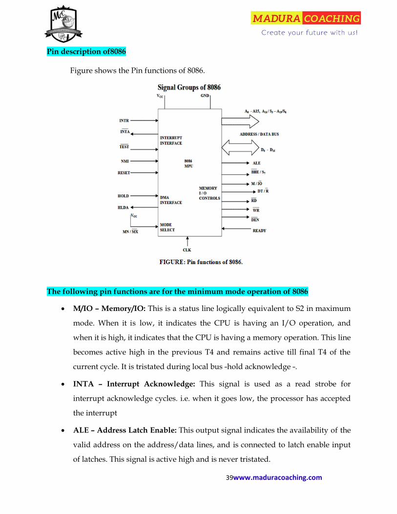
Pin Diagram of 8086 and Pin description of 8086
The following figure shows the Pin diagram of 8086. The description follows it.

36www.maduracoaching.com
The Microprocessor 8086 is a 16-bit CPU available in different clock rates and
packaged in a 40 pin CERDIP or plastic package.
The 8086 operates in single processor or multiprocessor configuration to achieve
high performance. The pins serve a particular function in minimum mode (single
processor mode) and other function in maximum mode configuration
(multiprocessor mode).
The 8086 signals can be categorized in three groups.
The first are the signal having common functions in minimum as well as
maximum mode.
The second are the signals which have special functions for minimum mode
The third are the signals having special functions for maximum mode.
The following signal descriptions are common for both modes.
AD15-AD0: These are the time multiplexed memory I/O address and data lines.

37www.maduracoaching.com
Address remains on the lines during T1 state, while the data is available on the
data bus during T2, T3 and T4. These lines are active high and float to a tristate
during interrupt acknowledge and local bus hold acknowledge cycles.
A19/S6, A18/S5, A17/S4, and A16/S3: These are the time multiplexed address
and status lines.
During T1 these are the most significant address lines for memory operations.
During I/O operations, these lines are low.
During memory or I/O operations, status information is available on those lines
for T2, T3 and T4.
The status of the interrupt enable flag bit is updated at the beginning of each
clock cycle.
The S4 and S3 combinely indicate which segment registers is presently being
used for memory accesses as in below fig.
These lines float to tri-state off during the local bus hold acknowledge. The status
line S6 is always low.
The address bit is separated from the status bit using latches controlled by the
ALE signal.
S4 S3 Indication
0
0
1
1
0
0
1
0
1
0
1
0
1
0
Alternate Data
Stack
Code or None
Data
Whole word
Upper byte from or to even address
Lower byte from or to even address

38www.maduracoaching.com
BHE/S7: The bus high enable is used to indicate the transfer of data over the
higher order (D15-D8) data bus as shown in table. It goes low for the data
transfer over D15-D8 and is used to derive chip selects of odd address memory
bank or peripherals. BHE is low during T1 for read, write and interrupt
acknowledge cycles, whenever a byte is to be transferred on higher byte of data
bus. The status information is available during T2, T3 and T4. The signal is active
low and tristated during hold. It is low during T1 for the first pulse of the
interrupt acknowledges cycle.
RD – Read: This signal on low indicates the peripheral that the processor is
performing memory or I/O read operation. RD is active low and shows the state
for T2, T3, and T4 of any read cycle. The signal remains tristated during the hold
acknowledge.
READY: This is the acknowledgement from the slow device or memory that they
have completed the data transfer. The signal made available by the devices is
synchronized by the 8284A clock generator to provide ready input to the 8086.
The signal is active high.
INTR-Interrupt Request: This is a triggered input. This is sampled during the
last clock cycles of each instruction to determine the availability of the request. If
any interrupt request is pending, the processor enters the interrupt acknowledge
cycle. This can be internally masked by resulting the interrupt enable flag. This
signal is active high and internally synchronized.
TEST: This input is examined by a ‗WAIT‘ instruction. If the TEST pin goes low,
execution will continue, else the processor remains in an idle state. The input is
synchronized internally during each clock cycle on leading edge of clock.
CLK- Clock Input: The clock input provides the basic timing for processor
operation and bus control activity. It‘s an asymmetric square wave with 33%
duty cycle.
39www.maduracoaching.com
Pin description of8086
Figure shows the Pin functions of 8086.
The following pin functions are for the minimum mode operation of 8086
M/IO – Memory/IO: This is a status line logically equivalent to S2 in maximum
mode. When it is low, it indicates the CPU is having an I/O operation, and
when it is high, it indicates that the CPU is having a memory operation. This line
becomes active high in the previous T4 and remains active till final T4 of the
current cycle. It is tristated during local bus ―hold acknowledge ―.
INTA – Interrupt Acknowledge: This signal is used as a read strobe for
interrupt acknowledge cycles. i.e. when it goes low, the processor has accepted
the interrupt
ALE – Address Latch Enable: This output signal indicates the availability of the
valid address on the address/data lines, and is connected to latch enable input
of latches. This signal is active high and is never tristated.

40www.maduracoaching.com
DT/R – Data Transmit/Receive: This output is used to decide the direction of
data flow through the transreceivers (bidirectional buffers). When the processor
sends out data, this signal is high and when the processor is receiving data, this
signal is low.
DEN – Data Enable: This signal indicates the availability of valid data over the
address/data lines. It is used to enable the transreceivers (bidirectional buffers)
to separate the data from the multiplexed address/data signal.
HOLD, HLDA- Acknowledge: When the HOLD line goes high, it indicates to
the processor that another master is requesting the bus access. The processor,
after receiving the HOLD request, issues the hold acknowledge signal on HLDA
pin, in the middle of the next clock cycle after completing the current bus cycle.
At the same time, the processor floats the local bus and control lines. When the
processor detects the HOLD line low, it lowers the HLDA signal. HOLD is an
asynchronous input, and is should be externally synchronized. If the DMA
request is made while the CPU is performing a memory or I/O cycle, it will
release the local bus during T4 provided:
1. The request occurs on or before T2 state of the current cycle.
2. The current cycle is not operating over the lower byte of a word.
3. The current cycle is not the first acknowledge of an interrupt
acknowledge sequence.
4. A Lock instruction is not being executed.
The following pin functions are applicable for maximum mode operation of 8086
S2, S1, and S0 – Status Lines: These are the status lines which reflect the type
of operation, being carried out by the processor. These become activity during
T4 of the previous cycle and active during T1 and T2 of the current bus cycles.
LOCK: This output pin indicates that other system bus master will be
prevented from gaining the system bus, while the LOCK signal is low. The

41www.maduracoaching.com
LOCK signal is activated by the ‗LOCK‘ prefix instruction and remains active
until the completion of the next instruction. When the CPU is executing a
critical instruction which requires the system bus, the LOCK prefix instruction
ensures that other processors connected in the system will not gain the control
of the bus.
The 8086, while executing the prefixed instruction, asserts the bus lock signal
output, which may be connected to an external bus controller. By prefetching
the instruction, there is a considerable speeding up in instruction execution in
8086. This is known as instruction pipelining.
S2 S1 S0 Indication
0
0
0
0
1
1
1
1
0
0
1
1
0
0
1
1
0
1
0
1
0
1
0
1
Interrupt Acknowledge
Read I/O port
Write I/O port
Halt
Code Access
Read Memory
Write Memory
Passive
At the starting the CS: IP is loaded with the required address from which the
execution is to be started. Initially, the queue will be empty and the
microprocessor starts a fetch operation to bring one byte (the first byte) of
instruction code, if the CS: IP address is odd or two bytes at a time, if the CS: IP
address is even.
The first byte is a complete opcode in case of some instruction (one byte opcode
instruction) and is a part of opcode, in case of some instructions (two byte

42www.maduracoaching.com
opcode instructions), the remaining part of code lie in second byte.
The second byte is then decoded in continuation with the first byte to decide the
instruction length and the number of subsequent bytes to be treated as
instruction data. The queue is updated after every byte is read from the queue
but the fetch cycle is initiated by BIU only if at least two bytes of the queue are
empty and the EU may be concurrently executing the fetched instructions.
The next byte after the instruction is completed is again the first opcode byte of
the next instruction. A similar procedure is repeated till the complete execution
of the program. The fetch operation of the next instruction is overlapped with
the execution of the current instruction. As in the architecture, there are two
separate units, namely Execution unit and Bus interface unit.
While the execution unit is busy in executing an instruction, after it is completely
decoded, the bus interface unit may be fetching the bytes of the next instruction
from memory, depending upon the queue status.
QS1 QS0 Indication
0
0
0
1
No Operation
First Byte of the opcode
from the queue
1
1
0
1
Empty Queue
Subsequent Byte from the
Queue
RQ/GT0, RQ/GT1 – Request/Grant: These pins are used by the other local bus
master in maximum mode, to force the processor to release the local bus at the
end of the processor current bus cycle.
Each of the pin is bidirectional with RQ/GT0 having higher priority than
RQ/GT1. RQ/GT pins have internal pull-up resistors and may be left

43www.maduracoaching.com
unconnected. Request/Grant sequence is as follows:
1. A pulse of one clock wide from another bus master requests the bus access
to8086.
2. During T4(current) or T1(next) clock cycle, a pulse one clock wide from 8086 to
the requesting master, indicates that the 8086 has allowed the local bus to float
and that it will enter the ‗hold acknowledge‘ state at next cycle. The CPU bus
interface unit is likely to be disconnected from the local bus of the system.
3. A one clock wide pulse from the master indicates to the 8086 that the hold
request is about to end and the 8086 may regain control of the local bus at the
next clock cycle. Thus each master to master exchange of the local bus is a
sequence of 3 pulses. There must be at least one dead clock cycle after each
bus exchange. The request and grant pulses are active low. For the bus request
those are received while 8086 is performing memory or I/O cycle, the granting
of the bus is governed by the rules as in case of HOLD and HLDA in
minimum mode.
ARCHITECTURE OF 8086 OR FUNCTIONAL BLOCK DIAGRAM OF8086
8086 has two blocks Bus Interfacing Unit (BIU) and Execution Unit(EU).
The BIU performs all bus operations such as instruction fetching, reading and
writing operands for memory and calculating the addresses of the memory
operands. The instruction bytes are transferred to the instruction queue.
EU executes instructions from the instruction system byte queue.
Both units operate asynchronously to give the 8086 an overlapping instruction
fetch and execution mechanism which is called as Pipelining. This results in
efficient use of the system bus and system performance.
BIU contains Instruction queue, Segment registers, Instruction pointer, and
Address adder.

44www.maduracoaching.com
EU contains Control circuitry, Instruction decoder, ALU, Pointer and Index
register, Flag register.
BUS INTERFACEUNIT
It provides a full 16 bit bidirectional data bus and 20 bit address bus.
The bus interface unit is responsible for performing all external bus operations.
Specifically it has the following functions:
Instruction fetches Instruction queuing, Operand fetch and storage, Address
relocation and Bus control.
The BIU use same mechanism known as an instruction stream queue to
implement pipeline architecture.
This queue permits prefetch of up to six bytes of instruction code. When ever the
queue of the BIU is not full, it has room for at least two more bytes and at the
same time the EU is not requesting it to read or write operands from memory, the
BIU is free to look ahead in the program by prefetching the next sequential
instruction.
FIGURE: Block diagram of 8086.
These prefetching instructions are held in its FIFO queue. With its 16 bit data bus,
the BIU fetches two instruction bytes in a single memory cycle.

45www.maduracoaching.com
After a byte is loaded at the input end of the queue, it automatically shifts up
through the FIFO to the empty location nearest the output.
The EU accesses the queue from the output end. It reads one instruction byte
after the other from the output of the queue. If the queue is full and the EU is not
requesting access to operand in memory.
These intervals of no bus activity, which may occur between bus cycles, are
known as Idle state.
If the BIU is already in the process of fetching an instruction when the EU request
it to read or write operands from memory or I/O, the BIU first completes the
instruction fetch bus cycle before initiating the operand read / write cycle.
The BIU also contains a dedicated adder which is used to generate the 20bit
physical address that is output on the address bus. This address is formed by
adding an appended 16 bit segment address and a 16 bit offset address.
For example: The physical address of the next instruction to be fetched is formed
by combining the current contents of the code segment CS register and the
current contents of the instruction pointer IP register.
The BIU is also responsible for generating bus control signals such as those for
memory read or write and I/O read or write.
EXECUTIONUNIT
The Execution unit is responsible for decoding and executing all instructions.
The EU extracts instructions from the top of the queue in the BIU, decodes
them, generates operands if necessary, passes them to the BIU and requests it
to perform the read or write bys cycles to memory or I/O and perform the
operation specified by the instruction on the operands.
During the execution of the instruction, the EU tests the status and control
flags and updates them based on the results of executing the instruction.

46www.maduracoaching.com
If the queue is empty, the EU waits for the next instruction byte to be fetched
and shifted to top of the queue.
When the EU executes a branch or jump instruction, it transfers control to a
location corresponding to another set of sequential instructions.
Whenever this happens, the BIU automatically resets the queue and then
begins to fetch instructions from this new location to refill the queue.
8086 REGISTERS
The 8086 microprocessor has a total of fourteen registers that are accessible to the
programmer. It is divided into four groups.
They are: Four General purpose registers Four Index/Pointer registers Four
Segment registers Two Other registers
General PurposeRegisters:
Accumulator register consists of two 8-bit registers AL and AH, which can be
combined together and used as a 16-bit register AX. AL in this case contains the low
order byte of the word, and AH contains the high-order byte. Accumulator can be used
for I/O operations and string manipulation.
Base register consists of two 8-bit registers BL and BH, which can be combined
together and used as a 16-bit register BX. BL in this case contains the low-order byte of
the word, and BH contains the high- order byte. BX register usually contains a data
pointer used for based, based indexed or register indirect addressing.
Count register consists of two 8-bit registers CL and CH, which can be combined
together and used as a 16-bit register CX. When combined, CL register contains the low

47www.maduracoaching.com
order byte of the word, and CH contains the high-order byte. Count register can be
used in Loop, shift/rotate instructions and as a counter in string manipulation.
Data register consists of two 8-bit registers DL and DH, which can be combined
together and used as a 16-bit register DX. When combined, DL register contains the low
order byte of the word, and DH contains the high-order byte. Data register can be used
as a port number in I/O operations. In integer 32-bit multiply and divide instruction the
DX register contains high-order word of the initial or resulting number.
Index or PointerRegisters
These registers can also be called as Special Purpose registers.
Stack Pointer (SP) is a 16-bit register pointing to program stack, ie it is used to
hold the address of the top of stack. The stack is maintained as a LIFO with its bottom at
the start of the stack segment (specified by the SS segment register).Unlike the SP
register, the BP can be used to specify the offset of other program segments.
Base Pointer (BP) is a 16-bit register pointing to data in stack segment. It is
usually used by subroutines to locate variables that were passed on the stack by a
calling program. BP register is usually used for based, based indexed or register indirect
addressing.
Source Index (SI) is a 16-bit register. SI is used for indexed, based indexed and
register indirect addressing, as well as a source data addressing string manipulation
instructions. Used in conjunction with the DS register to point to data locations in the
data segment.
Destination Index (DI) is a 16-bit register. Used in conjunction with the ES
register in string operations. DI is used for indexed, based indexed and register indirect
48www.maduracoaching.com
addressing, as well as a destination data address in string manipulation instructions. In
short, Destination Index and SI Source Index registers are used to hold address.
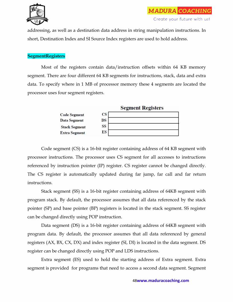
SegmentRegisters
Most of the registers contain data/instruction offsets within 64 KB memory
segment. There are four different 64 KB segments for instructions, stack, data and extra
data. To specify where in 1 MB of processor memory these 4 segments are located the
processor uses four segment registers.
Code segment (CS) is a 16-bit register containing address of 64 KB segment with
processor instructions. The processor uses CS segment for all accesses to instructions
referenced by instruction pointer (IP) register. CS register cannot be changed directly.
The CS register is automatically updated during far jump, far call and far return
instructions.
Stack segment (SS) is a 16-bit register containing address of 64KB segment with
program stack. By default, the processor assumes that all data referenced by the stack
pointer (SP) and base pointer (BP) registers is located in the stack segment. SS register
can be changed directly using POP instruction.
Data segment (DS) is a 16-bit register containing address of 64KB segment with
program data. By default, the processor assumes that all data referenced by general
registers (AX, BX, CX, DX) and index register (SI, DI) is located in the data segment. DS
register can be changed directly using POP and LDS instructions.
Extra segment (ES) used to hold the starting address of Extra segment. Extra
segment is provided for programs that need to access a second data segment. Segment

49www.maduracoaching.com
registers cannot be used in arithmetic operations.
Other registers of 8086
Instruction Pointer (IP) is a 16-bit register. This is a crucially important register
which is used to control which instruction the CPU executes. The ip, or program
counter, is used to store the memory location of the next instruction to be executed. The
CPU checks the program counter to ascertain which instruction to carry out next. It then
updates the program counter to point to the next instruction. Thus the program counter
will always point to the next instruction to be executed.
Flag Register contains a group of status bits called flags that indicate the status of
the CPU or the result of arithmetic operations. There are two types of flags:
1. The status flags which reflect the result of executing an instruction. The
programmer cannot set/reset these flags directly.
2. The control flags enable or disable certain CPU operations. The programmer
can set/reset these bits to control the CPU's operation.
Nine individual bits of the status register are used as control flags (3 of them)
and status flags (6 of them).The remaining 7 are not used. A flag can only take on the
values 0 and 1. We say a flag is set if it has the value 1.The status flags are used to
record specific characteristics of arithmetic and of logical instructions.

50www.maduracoaching.com
Control Flags: There are three control flags
The Direction Flag (D): Affects the direction of moving data blocks by such
instructions as MOVS, CMPS and SCAS. The flag values are 0 = up and 1 =
down and can be set/reset by the STD (set D) and CLD (clear D) instructions.
The Interrupt Flag (I): Dictates whether or not system interrupts can occur.
Interrupts are actions initiated by hardware block such as input devices that
will interrupt the normal execution of programs. The flag values are 0 = disable
interrupts or 1 = enable interrupts and can be manipulated by the CLI (clear I)
and STI (set I) instructions.
The Trap Flag (T): Determines whether or not the CPU is halted after the
execution of each instruction. When this flag is set (i.e. = 1), the programmer
can single step through his program to debug any errors. When this flag = 0
this feature is off. This flag can be set by the INT 3instruction.
Status Flags: There are six status flags
The Carry Flag (C): This flag is set when the result of an unsigned arithmetic
operation is too large to fit in the destination register. This happens when there is
an end carry in an addition operation or there an end borrows in a subtraction
operation. A value of 1 = carry and 0 = no carry.
The Overflow Flag (O): This flag is set when the result of a signed arithmetic
operation is too large to fit in the destination register (i.e. when an overflow

51www.maduracoaching.com
occurs). Overflow can occur when adding two numbers with the same sign (i.e.
both positive or both negative). A value of 1 = overflow and 0 = no overflow.
The Sign Flag (S): This flag is set when the result of an arithmetic or logic
operation is negative. This flag is a copy of the MSB of the result (i.e. the sign bit).
A value of 1 means negative and 0 =positive.
The Zero Flag (Z): This flag is set when the result of an arithmetic or logic
operation is equal to zero. A value of 1 means the result is zero and a value of 0
means the result is not zero.
The Auxiliary Carry Flag (A): This flag is set when an operation causes a carry
from bit 3 to bit 4 (or a borrow from bit 4 to bit 3) of an operand. A value of 1 =
carry and 0 = no carry.
The Parity Flag (P): This flags reflects the number of 1s in the result of an
operation. If the number of 1s is even its value = 1 and if the number of 1s is odd
then its value =0.
PROGRAMING MODEL
As a programmer of the 8086 or 8088 you must become familiar with the various
registers in the EU and BIU.
52www.maduracoaching.com
The data group consists of the accumulator and the BX, CX, and DX registers.
Note that each can be accessed as a byte or a word. Thus BX refers to the 16-bit
base register but BH refers only to the higher 8 bits of this register. The data
registers are normally used for storing temporary results that will be acted on by
sub sequential instructions.
The pointer and index group are all 16-bit registers (you cannot access the low or
high bytes alone). These registers are used as memory pointers. Sometimes a
pointer reg will be interpreted as pointing to a memory byte and at other times a
memory word. As you will see, the 8086/88 always stores words with the high-
order byte in the high-order word address.
Register IP could be considered in the previous group, but this register has only
one function -to point to the next instruction to be fetched to the BIU. Register IP
is physically part of the BIU and not under direct control of the programmer as
are the other pointer registers.
Six of the flags are status indicators, reflecting properties of the result of the last
arithmetic or logical instructions. The 8086/88 has several instructions that can
be used to transfer program control to a new memory location based on the state
of the flags.
Three of the flags can be set or reset directly by the programmer and are used to
control the operation of the processor. These are TF, IF, and DF.
The final group of registers is called the segment group. These registers are used
by the BIU to determine the memory address output by the CPU when it is
reading or writing from the memory unit. To fully understand these registers, we
must first study the way the 8086/88 divides its memory into segments.
MEMORY SEGMENTATION
Even though the 8086 is considered a 16-bit processor, (it has a 16-bit data bus
width) its memory is still thought of in bytes. At first this might seem a
disadvantage:

53www.maduracoaching.com
Why saddle a 16-bit microprocessor with an 8-bitmemory?
Actually, there are a couple of good reasons. First, it allows the processor to work
on bytes as well as words. This is especially important with I/O devices such as
printers, terminals, and modems, all of which are designed to transfer ASCII-
encoded (7- or 8-bit)data.
Second, many of the 8086's (and 8088's) operation codes are single bytes. Other
instructions may require anywhere from two to seven bytes. By being able to
access individual bytes, these odd-length instructions can be handled.
We have already seen that the 8086/88 has a 20-bit address bus, allowing it to
output 210, or 1'048.576, different memory addresses. As you can see, 524.288
words can also be visualized.
As mentioned, the 8086 reads 16 bits from memory by simultaneously reading an
odd-addressed byte and an even-addressed byte. For this reason the 8086
organizes its memory into an even-addressed bank and an odd-addressed bank.
With regard to this, you might wonder if all words must begin at an even
address. Well, the answer is yes. However, there is a penalty to be paid. The CPU
must perform two memory read cycles: one to fetch the low-order byte and a
second to fetch the high-order byte. This slows down the processor but is
transparent to the programmer.
The last few paragraphs apply only to the 8086. The 8088 with its 8-bit data bus
interfaces to the 1 MB of memory as a single bank. When it is necessary to access
a word (whether on an even- or an odd-addressed boundary) two memory read
(or write) cycles are performed. In effect, the 8088 pays a performance penalty
with every word access. Fortunately for the programmer, except for the slightly
slower performance of the 8088, there is no difference between the two
processors.

54www.maduracoaching.com
MEMORY MAP Still another view of the 8086/88 memory space could be as 16 64K-byte blocks
beginning at hex address 000000h and ending at address 0FFFFFh. This division into
64K-byte blocks is an arbitrary but convenient choice. This is because the most
significant hex digit increments by 1 with each additional block. That is, address 20000h
is 65.536 bytes higher in memory than address 10000h. Be sure to note that five hex
digits are required to represent a memory address.
The diagram is called a memory map. This is because, like a road map, it is a
guide showing how the system memory is allocated. This type of information is vital to
the programmer, who must know exactly where his or her programs can be safely
loaded.
Note that some memory locations are marked reserved and others dedicated.
The dedicated locations are used for processing specific system interrupts and the reset
function. Intel has also reserved several locations for future H/W and S/W products. If
you make use of these memory locations, you risk incompatibility with these future
products.
SEGMENT REGISTERS
Within the 1 MB of memory space the 8086/88 defines four 64K-byte memory
blocks called the code segment, stack segment, data segment, and extra segment. Each
of these blocks of memory is used differently by the processor.

55www.maduracoaching.com
The code segment holds the program instruction codes. The data segment stores
data for the program. The extra segment is an extra data segment (often used for shared
data). The stack segment is used to store interrupt and subroutine return addresses.
You should realize that the concept of the segmented memory is a unique one.
Older-generation microprocessors such as the 8-bit 8086 or Z-80 could access only one
64K-byte segment. This mean that the programs instruction, data and subroutine stack
all had to share the same memory. This limited the amount of memory available for the
program itself and led to disaster if the stack should happen to overwrite the data or
program are as.
The four segment registers (CS, DS, ES, and SS) are used to "point" at location 0
(the base address) of each segment. This is a little "tricky" because the segment registers
are only 16 bits wide, but the memory address is 20 bits wide. The BIU takes care of this
problem by appending four 0's to the low-order bits of the segment register. In effect,
this multiplies the segment register contents by16.
FIGURE: Memory segmentation in 8086.

56www.maduracoaching.com
The point to note is that the beginning segment address is not arbitrary -it must
begin at an address divisible by 16. Another way if saying this is that the low-order hex
digit must be 0.
Also note that the four segments need not be defined separately. Indeed, it is
allowable for all four segments to completely overlap (CS = DS = ES =SS).
Memory locations not defined to be within one of the current segments cannot be
accessed by the 8086/88 without first redefining one of the segment registers to include
that location. Thus at any given instant a maximum of 256 K (64K * 4) bytes of memory
can be utilized. As we will see, the contents of the segment registers can only be
specified via S/W. As you might imagine, instructions to load these registers should be
among the first given in any 8086/88program.
LOGICAL AND PHYSICAL ADDRESS
Addresses within a segment can range from address 00000h to address 0FFFFh.
This corresponds to the 64K-byte length of the segment. An address within a segment is
called an offset or logical address. A logical address gives the displacement from the
address base of the segment to the desired location within it, as opposed to its "real"
address, which maps directly anywhere into the 1 MB memory space. This "real"
address is called the physical address.
What is the difference between the physical and the logical address?
The physical address is 20 bits long and corresponds to the actual binary code
output by the BIU on the address bus lines. The logical address is an offset from
location 0 of a given segment.

57www.maduracoaching.com
FIGURE: Address calculation.
When two segments overlap it is certainly possible for two different logical
addresses to map to the same physical address. This can have disastrous results when
the data begins to overwrite the subroutine stack area, or vice versa. For this reason you
must be very careful when segments are allowed to overlap.
You should also be careful when writing addresses on paper to do so clearly. To
specify the logical address XXXX in the stack segment, use the convention SS:XXXX,
which is equal to [SS] * 16 + XXXX.
ADVANTAGES OF SEGMENTED MEMORY
Segmented memory can seem confusing at first. What you must remember is that
the program op-codes will be fetched from the code segment, while program data
variables will be stored in the data and extra segments. Stack operations use registers BP
or SP and the stack segment. As we begin writing programs the consequences of these
definitions will become clearer.
An immediate advantage of having separate data and code segments is that one
program can work on several different sets of data. This is done by reloading register
DS to point to the new data. Perhaps the greatest advantage of segmented memory is

58www.maduracoaching.com
that programs that reference logical addresses only can be loaded and run anywhere in
memory. This is because the logical addresses always range from 00000h to 0FFFFh,
independent of the code segment base. Such programs are said to be relocatable,
meaning that they will run at any location in memory. The requirements for writing
relocatable programs are that no references be made to physical addresses, and no
changes to the segment registers are allowed.
INTERRUPTS
Definition: The meaning of ‗interrupts‘ is to break the sequence of operation.
While the cpu is executing a program, on ‗interrupt‘ breaks the normal sequence of
execution of instructions, diverts its execution to some other program called Interrupt
Service Routine (ISR).After executing ISR , the control is transferred back again to the
main program. Interrupt processing is an alternative to polling.
Need for Interrupt: Interrupts are particularly useful when interfacing I/O
devices, that provide or require data at relatively low data transfer rate.
Types of Interrupts: There are two types of Interrupts in 8086. They are:
(i) Hardware Interrupts and (ii) Software Interrupts
Hardware Interrupts (External Interrupts). The Intel microprocessors
support hardware interrupts through:
Two pins that allow interrupt requests, INTR and NMI
INTR and NMI
INTR is a maskable hardware interrupt. The interrupt can be enabled/disabled
using STI/CLI instructions or using more complicated method of updating the
FLAGS register with the help of the POPF instruction.
When an interrupt occurs, the processor stores FLAGS register into stack,
disables further interrupts, fetches from the bus one by one representing
interrupt type, and jumps to interrupt.
Processing routine address of which is stored in location 4 * <interrupt type>.

59www.maduracoaching.com
Interrupt processing routine should return with the IRET instruction.
NMI is a non-maskable interrupt. Interrupt is processed in the same way as the
INTR interrupt. Interrupt type of the NMI is 2, i.e. the address of the NMI
processing routine is stored in location 0008h. This interrupt has higher priority
than the maskable interrupt.
Ex: NMI,INTR.
Software Interrupts (Internal Interrupts and Instructions) .Software interrupts can be
caused by:
INT instruction - breakpoint interrupt. This is a type 3 interrupt.
INT <interrupt number> instruction - any one interrupt from available 256
interrupts. INTO instruction - interrupt on overflow
Single-step interrupt - generated if the TF flag is set. This is a type 1 interrupt.
When the CPU processes this interrupt it clears TF flag before calling the
interrupt processing routine.
Processor exceptions: Divide Error (Type 0), Unused Opcode (type 6) and Escape
opcode (tpe 7). Software interrupt processing is the same as for the hardware
interrupts.
Ex: INT n (Software Instructions) Control is provided through:
IF and TF flag bits
IRET and IRETD

60www.maduracoaching.com
Performance of Software Interrupts
It decrements SP by 2 and pushes the flag register on the stack.
Disables INTR by clearing the IF.
It resets the TF in the flag Register.
It decrements SP by 2 and pushes CS on the stack.
It decrements SP by 2 and pushes IP on the stack.
Fetch the ISR address from the interrupt vector table.
Interrupt VectorTable

61www.maduracoaching.com
Functions associated with INT00 to INT04 INT 00 (divide error)
INT00 is invoked by the microprocessor whenever there is an attempt to divide a
number by zero. ISR is responsible for displaying the message ―Divide Error‖ on the
screen
INT 01
For single stepping the trap flag must be 1
After execution of each instruction, 8086 automatically jumps to 00004H to fetch
4 bytes for CS: IP of the ISR.
The job of ISR is to dump the registers on to the screen
INT 02 (Non maskable Interrupt)
When ever NMI pin of the 8086 is activated by a high signal (5v), the CPU Jumps
to physical memory location 00008 to fetch CS:IP of the ISR assocaiated with
NMI.

62www.maduracoaching.com
INT 03 (break point)
A break point is used to examine the CPU and memory after the execution of a
group of Instructions.
o It is one byte instruction
INT 04 (Signed number overflow)
There is an instruction associated with this INT 0 (interrupt on overflow).
If INT 0 is placed after a signed number arithmetic as IMUL or ADD the CPU
will activate INT 04 if 0F = 1.
In case where 0F = 0, the INT 0 is not executed but is bypassed and acts as a NOP.
Performance of Hardware Interrupts
NMI: Non maskable interrupts - TYPE 2 Interrupt
INTR: Interrupt request - Between 20H and FFH
Interrupt Priority Structure
General BusOperation
The 8086 has a combined address and data bus commonly referred as a time

63www.maduracoaching.com
multiplexed address and data bus.
The main reason behind multiplexing address and data over the same pins is the
maximum utilization of processor pins and it facilitates the use of 40 pin
standard DIP package.
The bus can be demultiplexed using a few latches and transreceivers, when ever
required.
Basically, all the processor bus cycles consist of at least four clock cycles. These
are referred to as T1, T2, T3, and T4. The address is transmitted by the processor
during T1. It is present on the bus only for one cycle.
The negative edge of this ALE pulse is used to separate the address and the data
or status information. In maximum mode, the status lines S0, S1 and S2 are used
to indicate the type of operation.
Status bits S3 to S7 are multiplexed with higher order address bits and the BHE
signal. Address is valid during T1 while status bits S3 to S7 are valid during T2
throughT4.
FIGURE: bus operation signal.
Maximum mode
In the maximum mode, the 8086 is operated by strapping the MN/MX pin to

64www.maduracoaching.com
ground.
In this mode, the processor derives the status signal S2, S1, S0. Another chip
called bus controller derives the control signal using this status information.
In the maximum mode, there may be more than one microprocessor in the
system configuration.
Minimum mode
In a minimum mode 8086 system, the microprocessor 8086 is operated in
minimum mode by strapping its MN/MX pin to logic1.
In this mode, all the control signals are given out by the microprocessor chip
itself.
There is a single microprocessor in the minimum mode system.
MINIMUM MODE 8086SYSTEM
In a minimum mode 8086 system, the microprocessor 8086 is operated in
minimum mode by strapping its MN/MX pin to logic 1.
In this mode, all the control signals are given out by the microprocessor chip
itself. There is a single microprocessor in the minimum mode system.
The remaining components in the system are latches, transreceivers, clock
generator, memory and I/O devices. Some type of chip selection logic may be
required for selecting memory or I/O devices, depending upon the address map
of the system.
Latches are generally buffered output D-type flip-flops like 74LS373 or 8282.
They are used for separating the valid address from the multiplexed
address/data signals and are controlled by the ALE signal generated by8086.
Transreceivers are the bidirectional buffers and some times they are called as
data amplifiers. They are required to separate the valid data from the time

65www.maduracoaching.com
multiplexed address/data signals.
They are controlled by two signals namely, DEN and DT/R.
The DEN signal indicates the direction of data, i.e. from or to the processor. The
system contains memory for the monitor and users program storage.
Usually, EPROM is used for monitor storage, while RAM for user‘s program
storage. A system may contain I/O devices.
Write Cycle Timing Diagram for MinimumMode
The working of the minimum mode configuration system can be better described
in terms of the timing diagrams rather than qualitatively describing the
operations.
The opcode fetch and read cycles are similar. Hence the timing diagram can be
categorized in two parts, the first is the timing diagram for read cycle and the
second is the timing diagram for write cycle.
The read cycle begins in T1 with the assertion of address latch enable (ALE)
signal and also M / IO signal. During the negative going edge of this signal, the
valid address is latched on the local bus.
The BHE and A0 signals address low, high or both bytes. From T1 to T4, the
M/IO signal indicates a memory or I/O operation.
AtT2,the address is removed from the local bus and is sent to the output. The bus
is then tristated.
The read (RD) control signal is also activated in T2.
The read (RD) signal causes the address device to enable its data bus drivers.
After RD goes low, the valid data is available on the databus.
The addressed device will drive the READY line high. When the processor

66www.maduracoaching.com
returns the read signal to high level, the addressed device will again tristate its
bus drivers.
A write cycle also begins with the assertion of ALE and the emission of the
address. The M/IO signal is again asserted to indicate a memory or I/O
operation. In T2, after sending the address in T1, the processor sends the data to
be written to the addressed location.
The data remains on the bus until middle of T4 state. The WR becomes active at
the beginning of T2 (unlike RD is somewhat delayed in T2 to provide time for
floating).
FIGURE: Write Cycle Timing Diagram for Minimum Mode
The BHE and A0 signals are used to select the proper byte or bytes of memory or
I/O word to be read or write.
The M/IO, RD and WR signals indicate the type of data transfer as specified in
table below.

67www.maduracoaching.com
Bus Request and Bus Grant Timings in Minimum Mode System of8086
Hold Response sequence: The HOLD pin is checked at leading edge of each clock
pulse. If it is received active by the processor before T4 of the previous cycle or
during T1 state of the current cycle, the CPU activates HLDA in the next clock
cycle and for succeeding bus cycles, the bus will be given to another requesting
master.
The control of the bus is not regained by the processor until the requesting
master does not drop the HOLD pin low. When the request is dropped by the
requesting master, the HLDA is dropped by the processor at the trailing edge of
the next clock.
T1 state of the current cycle, the CPU activates HLDA in the next clock cycle and
for succeeding bus cycles, the bus will be given to another requesting master.
The control of the bus is not regained by the processor until the requesting
master does not drop the HOLD pin low. When the request is dropped by the
requesting master, the HLDA is dropped by the processor at the trailing edge of
the next clock.
Minimum Mode Interface
When the Minimum mode operation is selected, the 8086 provides all control
signals needed to implement the memory and I/O interface.
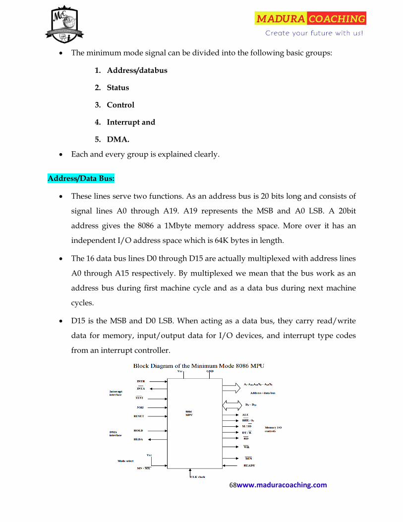
68www.maduracoaching.com
The minimum mode signal can be divided into the following basic groups:
1. Address/databus
2. Status
3. Control
4. Interrupt and
5. DMA.
Each and every group is explained clearly.
Address/Data Bus:
These lines serve two functions. As an address bus is 20 bits long and consists of
signal lines A0 through A19. A19 represents the MSB and A0 LSB. A 20bit
address gives the 8086 a 1Mbyte memory address space. More over it has an
independent I/O address space which is 64K bytes in length.
The 16 data bus lines D0 through D15 are actually multiplexed with address lines
A0 through A15 respectively. By multiplexed we mean that the bus work as an
address bus during first machine cycle and as a data bus during next machine
cycles.
D15 is the MSB and D0 LSB. When acting as a data bus, they carry read/write
data for memory, input/output data for I/O devices, and interrupt type codes
from an interrupt controller.

69www.maduracoaching.com
Status signal:
The four most significant address lines A19 through A16 are also multiplexed but
in this case with status signals S6 through S3. These status bits are output on the
bus at the same time that data are transferred over the other bus lines.
Bit S4 and S3 together from a 2 bit binary code that identifies which of the 8086
internal segment registers are used to generate the physical address that was
output on the address bus during the current bus cycle. Code S4S3 = 00 identifies
a register known as extra segment register as the source of the segment address.
Status line S5 reflects the status of another internal characteristic of the 8086. It is
the logic level of the internal enable flag. The last status bit S6 is always at the
logic 0level.
S4 S3
Segment Register
0
0
1
1
0
1
0
1
Extra Stack
Code / none
Data
Memory segment status codes
Control Signals:
The control signals are provided to support the 8086 memory I/O interfaces.
They control functions such as when the bus is to carry a valid address in which
direction data are to be transferred over the bus, when valid write data are on the
bus and when to put read data on the system bus.
ALE is a pulse to logic 1 that signals external circuitry when a valid address word
is on the bus. This address must be latched in external circuitry on the 1-to-0 edge
of the pulse at ALE.

70www.maduracoaching.com
Another control signal that is produced during the bus cycle is BHE bank high
enable. Logic 0 on this used as a memory enable signal for the most significant
byte half of the data bus D8 through D1. These lines also serves a second
function, which is as the S7 status line.
Using the M/IO and DT/R lines, the 8086 signals which type of bus cycle is in
progress and in which direction data are to be transferred over the bus. The logic
level of M/IO tells external circuitry whether a memory or I/O transfer is taking
place over the bus. Logic 1 at this output signals a memory operation and logic 0
an I/O operation.
The direction of data transfer over the bus is signaled by the logic level output at
DT/R. When this line is logic 1 during the data transfer part of a bus cycle, the
bus is in the transmit mode. Therefore, data are either written into memory or
output to an I/O device. On the other hand, logic 0 at DT/R signals that the bus
is in the receive mode. This corresponds to reading data from memory or input
of data from an input port.
The signal read RD and write WR indicates that a read bus cycle or a write bus
cycle is in progress. The 8086 switches WR to logic 0 to signal external device that
valid write or output data are on the bus.
On the other hand, RD indicates that the 8086 is performing a read of data of the
bus. During read operations, one other control signal is also supplied. This is
DEN (data enable) and it signals external devices when they should put data on
the bus. There is one other control signal that is involved with the memory and
I/O interface. This is the READY signal.
READY signal is used to insert wait states into the bus cycle such that it is
extended by a number of clock periods. This signal is provided by an external
clock generator device and can be supplied by the memory or I/O sub-system to
signal the 8086 when they are ready to permit the data transfer to be completed.

71www.maduracoaching.com
Interrupt signals:
The key interrupt interface signals are interrupt request (INTR) and interrupt
acknowledge (INTA). INTR is an input to the 8086 that can be used by an
external device to signal that it need to be serviced.
Logic 1 at INTR represents an active interrupt request. When an interrupt request
has been recognized by the 8086, it indicates this fact to external circuit with
pulse to logic 0 at the INTA output.
The TEST input is also related to the external interrupt interface. Execution of a
WAIT instruction causes the 8086 to check the logic level at the TEST input.
If the logic 1 is found, the MPU suspend operation and goes into the idle state.
The 8086 no longer executes instructions; instead it repeatedly checks the logic
level of the TEST input waiting for its transition back to logic0.
As TEST switches to 0, execution resume with the next instruction in the
program. This feature can be used to synchronize the operation of the 8086 to an
event in external hardware.
There are two more inputs in the interrupt interface: the nonmaskable interrupt
NMI and the reset interrupt RESET.
On the 0-to-1 transition of NMI control is passed to a non maskable interrupt
service routine. The RESET input is used to provide a hardware reset for the
8086. Switching RESET to logic 0 initializes the internal register of the 8086 and
initiates a reset service routine.
DMA Interface signals:
The direct memory access DMA interface of the 8086 minimum mode consist of
the HOLD and HLDA signals.
When an external device wants to take control of the system bus, it signals to the
8086 by switching HOLD to the logic 1 level. At the completion of the current bus

72www.maduracoaching.com
cycle, the 8086 enters the hold state. In the hold state, signal lines AD0 through
AD15, A16/S3 through A19/S6, BHE, M/IO, DT/R, RD, WR, DEN and INTR are
all in the high Z state.
The 8086 signals external device that it is in this state by switching its HLDA
output to logic 1 level.
Figure: Minimum Mode Interface
MAXIMUM MODE 8086SYSTEM
In the maximum mode, the 8086 is operated by strapping the MN/MX pin to
ground.
In this mode, the processor derives the status signal S2, S1, S0. Another chip
called bus controller derives the control signal using this status information.
In the maximum mode, there may be more than one microprocessor in the
system configuration. The components in the system are same as in the
minimum mode system.

73www.maduracoaching.com
The basic function of the bus controller chip IC8288 is to derive control signals
like RD and WR (for memory and I/O devices,) DEN, DT/R, ALE etc. using the
information by the processor on the status lines.
The bus controller chip has lines S2,S1,S0 and CLK. These inputs to 8288 are
driven by CPU.
It derives the outputs ALE, DEN, DT/R, MRDC, MWTC, AMWC, IORC, IOWC
and AIOWC. The AEN, IOB and CEN pins are especially useful for
multiprocessor system.
Figure: Maximum mode of operation
AEN and IOB are generally grounded. CEN pin is usually tied to +5V. The
significance of the MCE/PDEN output depends upon the status of the IOB pin.
If IOB is grounded, it acts as master cascade enable to control cascade 8259A, else
it acts as peripheral data enable used in the multiple bus configurations.
INTA pin used to issue two interrupt acknowledge pulses to the interrupt
controller or to an interrupting device.

74www.maduracoaching.com
IORC, IOWC are I/O read command and I/O write command signals
respectively. These signals enable an IO interface to read or write the data from
or to the address port.
The MRDC, MWTC are memory read command and memory write command
signals respectively and may be used as memory read or write signals.
All these command signals instructs the memory to accept or send data from or
to the bus.
For both of these write command signals, the advanced signals namely AIOWC
and AMWTC are available.
Here the only difference between in timing diagram between minimum mode
and maximum mode is the status signals used and the available control and
advanced command signals.
R0, S1, S2 are set at the beginning of bus cycle. 8288 bus controller will output a
pulse as on the ALE and apply a required signal to its DT/R pin during T1.
In T2, 8288 will set DEN=1 thus enabling transceivers, and for an input it will
activate MRDC or IORC. These signals are activated until T4. For an output, the
AMWC or AIOWC is activated from T2 to T4 and MWTC or IOWC is activated
from T3 to T4.
When the 8086 is set for the maximum-mode configuration, it provides signals
for implementing a multiprocessor / coprocessor system environment.
By multiprocessor environment we mean that one microprocessor exists in the
system and that each processor is executing its own program.

75www.maduracoaching.com
Memory Read Timing Diagram in Maximum Mode of8086
FIGURE: Memory Read Timing Diagram in Maximum Mode of 8086
Memory Write Timing in Maximum mode of8086
Figure: Memory Write Timing in Maximum mode of 8086

76www.maduracoaching.com
RQ/GT Timings in MaximumMode
Figure: Interface between MPU and Memory in maximum mode
8288 Bus Controller – Bus Command and Control Signals
8086 does not directly provide all the signals that are required to control the
memory, I/O and interrupt interfaces.
Specially the WR, M/IO, DT/R, DEN, ALE and INTA, signals are no longer
produced by the 8086. Instead it outputs three status signals S0, S1, S2 prior to
the initiation of each bus cycle. This 3- bit bus status code identifies which type
of bus cycle is to follow.

77www.maduracoaching.com
S2S1S0 are input to the external bus controller device, the bus controller
generates the appropriately timed command and control signals.
S2 S1 S0 Indication 8288
Command
0
0
0
0
0
1
0
1
0
Interrupt Acknowledge
Read I/O port
Write I/O port
INTA
IORC
0
1
1
1
1
1
0
0
1
1
1
0
1
0
1
Halt
Instruction Fetch
Read Memory
Write Memory
Passive
IOWC ,
AIOWC
None
MRDC
MRDC
MWTC,
AMWC
None
The 8288 produces one or two of these eight command signals for each bus
cycles. For instance, when the 8086 outputs the code S2S1S0 equals 001; it
indicates that an I/O read cycle is to be performed.
In the code 111 is output by the 8086, it is signaling that no bus activity is to take
place.

78www.maduracoaching.com
The control outputs produced by the 8288 are DEN, DT/R and ALE. These 3
signals provide the same functions as those described for the minimum system
mode. This set of bus commands and control signals is compatible with the Multi
bus and industry standard for interfacing microprocessor systems.
The output of 8289 are bus arbitration signals:
Bus busy (BUSY), common bus request (CBRQ), bus priority out (BPRO), bus priority in
(BPRN), bus request (BREQ) and bus clock (BCLK).
They correspond to the bus exchange signals of the Multibus and are used to
lock other processor off the system bus during the execution of an instruction by
the8086.
In this way the processor can be assured of uninterrupted access to common
system resources such as global memory.
Queue Status Signals: Two new signals that are produced by the 8086 in the
maximum-mode system are queue status outputs QS0 and QS1. Together they
form a 2-bit queue status code, QS1QS0.
Following table shows the four different queue status.
QS1 QS0 Queue Status
0 (low) 0 Queue Empty. The queue has been reinitialized
as a result of the execution of a transfer instruction.
0 1 First Byte. The byte taken from the queue was the
first byte of the instruction.
1 0 Queue Empty. The queue has been reinitialized
as a result of the execution of a transfer instruction.
1 1 Subsequent Byte. The byte taken from the queue
was a subsequent byte of the instruction.

79www.maduracoaching.com
Local Bus Control Signal – Request / Grant Signals: In a maximum mode
configuration, the minimum mode HOLD, HLDA interface is also changed.
These two are replaced by request/grant lines RQ/ GT0 and RQ/ GT1,
respectively. They provide a prioritized bus access mechanism for accessing the
local bus.
Instruction Set and Addressing Modes of the 8086 Microprocessor
An instruction is a basic command given to a microprocessor to perform a
specified operation with given data. Each instruction has two groups of bits. One group
of bits is known as operation code (opcode), which defines what operation will be
performed by the instruction. The other field is called operand, which specifies data that
will be used in arithmetic and logical operations. The addressing mode is used to locate
the operand or data. There are different types of addressing modes depending upon the
location of data in the 8086 processor.
The instruction format should have one or more number of fields to represent
instruction. The first field is called operation code or opcode fields, and other fields are
known as operand fields. The microprocessor executes the instruction based on the
information of opcode and operand fields.
In this chapter, the general instruction format and different addressing modes of
8086/8088 processor along with examples are discussed. All types of instructions with
examples are discussed elaborately. This chapter creates a background for assembly-
language programming in 8086/8088 processor.
ADDRESSING MODES
An instruction is divided into operation code (opcode) and operands. The
opcode is a group of bits which indicates what operation can be performed by the
processor. An operand is also known as data (datum) and it can identify the source and
destination of data. The operand can specify a register or a memory location in any one

80www.maduracoaching.com
of the memory segments or I/O ports. Figure shows a general instruction format which
consists of six bytes. Some instructions have only an opcode and such
Fig.: General 8086 instruction format
instructions are called single-byte instructions. Some instructions contain one- or two-or
three- or four-byte operands. The detailed operation of instruction sets is explained in
Section 6.3.
There are different ways to specify an operand. Each way of how an operand can
be specified is called an addressing mode. The different addressing modes of 8086
microprocessors are as follows:
Immediate addressing
Register addressing
Memory addressing
Branch addressing
Immediate Addressing
In this mode of addressing, the 8-bit or 16-bit operand is a part of the instruction.
For example, MOV AX, 4000H. In this instruction, the data 4000H can be loaded to the
AX register immediately. Some other examples are given below:
MOV BX, 7000H; load 7000H in BX register
MOV CX, 4500H; store 4500H in CX register
Register Addressing
In the 8086 microprocessor, some instructions are operated on the general-
purpose registers. The data is in the register specified by the instruction. The format for
register addressing is

81www.maduracoaching.com
MOV Destination, Source
In this instruction, the data from the source register can be copied into the
destination register. The 8-bitregisters (AL, AH, BL, BH, CL, CH, DL, DH) and 16-bit
registers (AX, BX, CX, DX, SI, DI, SP, BP) may be used for this instruction. The only
restriction is that both operands must be of the same length. For example,
MOV AL, BL; Copies the value of BL into AL
MOV AX, BX; Copies the contents of BX into AX
Memory Addressing
Memory addressing requires determination of physical address. The physical
address can be computed from the content of segment address and an effective address.
The segment address identifies the starting location of the segment in the memory and
effective address represents the offset of the operand from the beginning of this
segment of memory. The 20-bit effective address can be made up of base, index, and
displacement. The basic formula for the 16-bit effective address (EA) and the 20-bit
physical address (PA) is given below:
16-bit EA = Base + Index + Displacement
20-bit PA = Segment × 10 + Base + Index + Displacement
Memory addressing has the following combinations:
Direct addressing
Register indirect addressing
Based addressing
Indexed addressing
Based Indexed addressing
Based Indexed with displacement addressing
Direct Addressing
In this mode of addressing, the instruction operand specifies the memory
address where data is located. This addressing mode is similar to the immediate
addressing mode, but the opcode follows an effective address instead of data. This is

82www.maduracoaching.com
the most common addressing mode. The displacement-only addressing mode consists
of an 8-bit or 16-bit constant that specifies the offset of the actual address of the target
memory location. For example, MOV AX, [5000] copies 2 bytes of data starting from
memory location DS × 10 + 5000H to the AX register. The lower byte is at the location
DS × 10 + 5000H and the higher byte will be at the location DS × 10 + 5001H. Another
example is MOV AL, DS: [5000H]. In this instruction, the content of the memory
location DS × 10 + 5000H loads into the AL register.
The instruction MOV DS:[2000H], AL means that the content of the AL register
will move to memory location DS × 10 + [2000H]. The computation of memory location
for the operand is illustrated in Fig. In this figure, the effective address (EA) is 2000H
and the physical address (PA) is PA = DS × 10 + EA = 4000 × 10 + 2000 = 42000. The
physical address (PA) computation for other segment registers with same effective
address is given below:
PA = CS × 10 + EA, PA = SS × 10 + EA, and PA = ES × 10 + EA.
Generally, all displacement values or offsets are added with the data segment to
determine the physical address. If something other than a data segment is required, we
must use a segment override prefix before the address. For example, to access memory
location 4000H in the Stack Segment (SS), the instruction will be MOV AX, SS: [2000H].
Similarly, to access the memory location in the Extra Segment (ES), the instruction will
be written as MOV AX, ES: [2000H].
Fig.: Direct memory addressing

83www.maduracoaching.com
Register Indirect Addressing
This instruction specifies a register containing an address, where data is located.
The effective address of the data is in the base register BX or an index register that is
specified by the instruction. This addressing mode works with index registers SI, DI,
and base registers BX and BP registers.
The BX, BP, SI, or DI registers are using the DS segment by default. The base
pointer uses stack segment by default. The segment override prefix symbols are used to
access data in different segments.
The effective address EA may either be in a base register (BX or BP) or in an
index register (SI and DI). The physical address can be computed based on contents of
segment register, BX, BP, SI and DI registers as given below: PA = CS × 10 + BX, PA =
DS × 10 + BP, PA = SS × 10 + DI, and PA = ES × 10 + SI.
The general physical address expression for register indirect memory operand is
depicted in Fig. The content of BX is 1000H and CS is 2000. Then the physical address is
CS × 10 + BX = 2000 × 10 + 1000 = 21000H. After executing the MOV AL, [BX]
instruction, the contents of the memory location 21000H is 44H which will be stored in
the AL register.
Based Addressing
The 8-bit or 16-bit instruction operand is added to the contents of a base register
(BX or BP), the resulting value is a pointer to the location where the data resides. The
effective address in based addressing mode is obtained by adding the direct or indirect
displacement to the contents of either the base register BX or the base pointer BP. The
effective address and physical address computation are given below:

84www.maduracoaching.com
Fig.: Register indirect addressing
EA = BX + 8-bit displacement EA = BP + 8-bit displacement
EA = BX + 16-bit displacement EA = BP + 16-bit displacement
PA = Segment × 10 + BX + 8-bit displacement, PA = Segment × 10 + BP + 8-bit
displacement
PA = Segment × 10 + BX + 16-bit displacement, PA = Segment × 10 + BP + 16-
bit displacement
Segment will be any one of the segments CS, DS, SS and ES. Figure shows the
physical address computation in base addressing mode. When 16-bit displacement
DISP = 0025H, the contents of the BX register is 0500H and the contents of the DS
register is 4000H, the physical address = DS × 10 + BX + DISP = 4000H × 10 + 0500 +
0025 = 40525H. After execution of MOV AL, DS: [BX+DISP] instruction, the contents of
the memory location 40525H will be copied into the AL register.
Fig.: Base addressing

85www.maduracoaching.com
Indexed Addressing
These addressing modes can work similar to the based addressing mode. The 8-
bit or 16-bit instruction operand is added to the contents of an index register (SI or DI),
and the resulting value is a pointer to the location where the data resides.
The displacement value is used as a pointer to the starting point of an array of
data in memory and the contents of the specified register is used as an index. The EA
and PA in the indexed addressing are as follows:
EA = SI + 8-bit displacement EA = DI + 8-bit displacement
EA = SI + 16-bit displacement EA = DI + 16-bit displacement
PA = Segment × 10 + SI + 8 bit displacement PA = Segment × 10 + DI + 8 bit
displacement
PA = Segment × 10 + SI + 16 bit displacement PA = Segment × 10 + SI + 16 bit
displacement
Segment will be any one of segment registers (CS, DS, SS and ES).
The index addressing modes generally involve BX, SI, and DI registers with the
data segment. The [BP+DISP] addressing mode uses the stack segment by default. In
the register indirect addressing modes, the segment override prefixes can be used to
specify different segments.
Figure shows the physical address computation in index addressing mode. When
16-bit displacement DISP = 0055H, the contents of SI is 0100H and the contents of DS
register is 4000H, the physical address = DS × 10 + SI + DISP = 4000H × 10 + 0100 + 0055
= 40155H. If MOV AL, DS: [SI + 0025] is executed, the contents of the memory location
40155H, FF will be loaded into the AL register. Figure shows the indexed addressing.

86www.maduracoaching.com
Fig.: Indexed addressing
Based Indexed Addressing
The contents of a base register (BX or BP) is added to the contents of an index
register (SI or DI),the resulting value is a pointer to the location where the data resides.
The effective address is the sum of a base register and an index register which are
specified in the instruction. The based indexed addressing modes are simply
combinations of the register indirect addressing modes. These addressing modes form
the offset by adding together a base register (BX or BP) and an index register (SI or DI).
The EA and the PA computation are given below:
EA = BX + SI, EA = BX + DI
EA = BP + SI, EA = BP + DI
PA = Segment × 10 + BX + SI
PA = Segment × 10 + BX + DI
PA = Segment × 10 + BP + SI
PA = Segment × 10 + BP + DI

87www.maduracoaching.com
Fig.: Based indexed addressing
Figure shows the physical address computation in based indexed addressing
mode. For example, if the content of BX register is 0200H and SI contains 0100H. Then
the instruction MOV AL, [BX + SI] loads the content of the memory location DS × 10 +
BX + SI into the AH register. If DS = 4000H, the memory location address is 4000 × 10 +
0200 + 0100 = 40300H whose content 66H will be loaded into the AH register. The
examples of this addressing mode instruction are as follows:
MOV AL, [BX + DI] MOV AL, [BX + SI]
MOV AL, [BP + SI] MOV AL, [BP + DI]
Based Indexed with Displacement Addressing
The 8-bit or 16-bit instruction operand is added to the contents of a base register
(BX or BP) and index register (SI or DI), the resulting value is a pointer to the location
where the data resides. The effective address is the sum of an 8-bit or 16-bit
displacement and based index address. The computation of EA and the PA are given
below:
EA = BX + SI + 8-bit or 16-bit instruction EA = BX + DI 8-bit or 16-bit instruction
EA = BP + SI + 8-bit or 16-bit instruction EA = BP + DI 8-bit or 16-bit instruction
PA = Segment × 10 + BX + SI + 8-bit or 16-bit instruction
PA = Segment × 10 + BX + DI + 8-bit or 16-bit instruction
PA = Segment × 10 + BP + SI + 8-bit or 16-bit instruction
PA = Segment × 10 + BP + DI+ 8-bit or 16-bit instruction

88www.maduracoaching.com
Figure shows the physical address computation in based indexed with
displacement addressing mode. When 16-bit displacement DISP = 0020H, the contents
of BX register is 4000H, the contents of SI is 0300 and the contents of DS register is
5000H, the physical address = DS × 10 + BX + SI + DISP = 5000H × 10 + 4000 + 0300 +
0020 = 54320H. When MOV AL, DS:[BX + SI + DISP] is executed, the content of the
memory location 54320H will be copied into the AL register.
Fig.: Based indexed with displacement addressing
String Addressing Mode
String is a sequence of bytes or words which are stored in memory. Stored
characters in word processors and data table are examples of string. Some instructions
are designed to handle a string of characters or data. These instructions have a special
addressing mode where DS : SI is used as a source of string and ES:DI is used to locate
the destination address of the string. For example, MOV SB instruction is used to move
a string of source data to the destination location.
When any MOV instruction is executed, data is always transferred from source
to destination. The MOV instruction for different addressing modes is depicted in Table
A. The effective address computation depends on MOD and R/M bit patterns as shown
in Table B. Segment registers for different addressing modes may be different and its
selection also depends on MOD and R/M as illustrated in Table C.
Table A-MOV instruction

89www.maduracoaching.com
Table B: Effective addressing computations corresponding to MOD and R/M fields

90www.maduracoaching.com
Table C: Segment registers for different addressing modes corresponding to MOD
and R/M fields
Branch Addressing
The basic types of branch addressing are shown in Fig. 6.8. The intra segment
mode is used to transfer the control to a destination that lies in the same segment where
the control transfer instruction itself resides. In the intersegment mode, address is used
to transfer the control to a destination that lies in a different segment.
For the branch-control transfer instructions, the addressing modes depend upon
whether the destination location is within the same segment or in a different one. It
depends upon the method of passing the destination address to the processor. There are
two types of branch control instructions: intersegment and intrasegment addressing
modes.
During execution of program instruction, when the location to which the control
to be transferred lies in a different segment other than the current one, the mode is
called intersegment mode. If the destination location lies in the same segment, the mode
is called intrasegment mode.
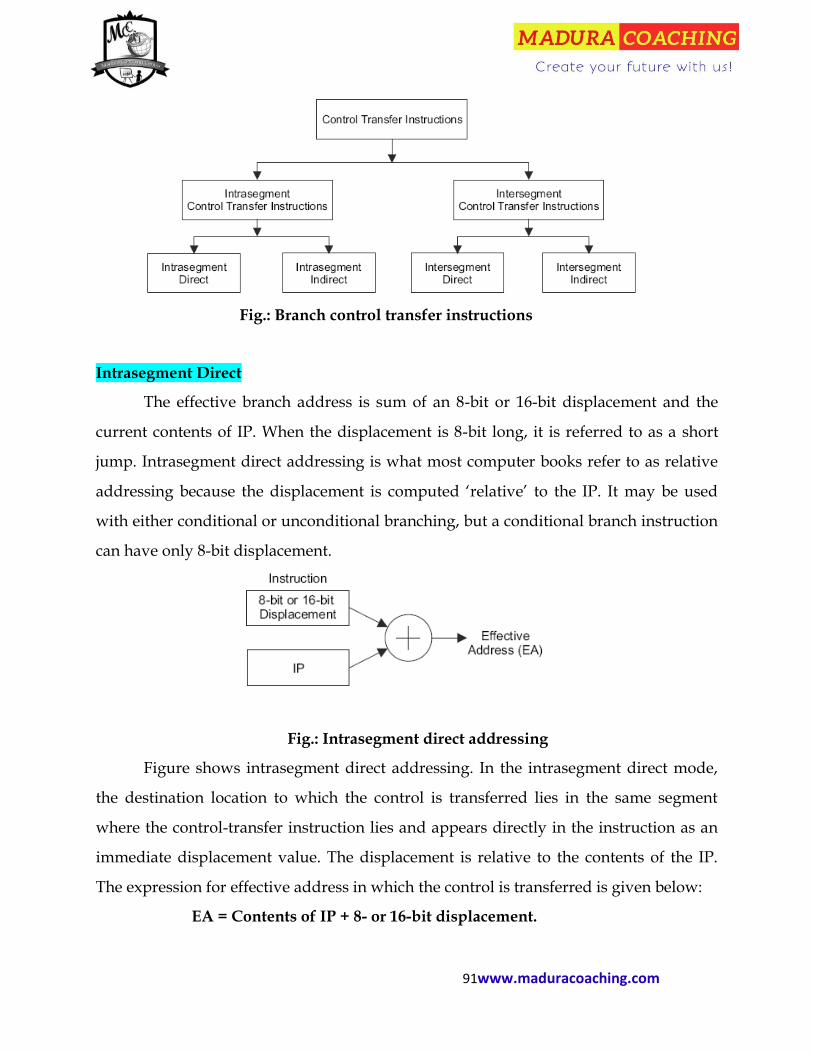
91www.maduracoaching.com
Fig.: Branch control transfer instructions
Intrasegment Direct
The effective branch address is sum of an 8-bit or 16-bit displacement and the
current contents of IP. When the displacement is 8-bit long, it is referred to as a short
jump. Intrasegment direct addressing is what most computer books refer to as relative
addressing because the displacement is computed ‘relative’ to the IP. It may be used
with either conditional or unconditional branching, but a conditional branch instruction
can have only 8-bit displacement.
Fig.: Intrasegment direct addressing
Figure shows intrasegment direct addressing. In the intrasegment direct mode,
the destination location to which the control is transferred lies in the same segment
where the control-transfer instruction lies and appears directly in the instruction as an
immediate displacement value. The displacement is relative to the contents of the IP.
The expression for effective address in which the control is transferred is given below:
EA = Contents of IP + 8- or 16-bit displacement.

92www.maduracoaching.com
Intrasegment Indirect
The effective branch address is the contents of a register or memory location that
is accessed using any of the above data-related addressing modes except the immediate
mode. The contents of IP are replaced by the effective branch address. This addressing
mode may be used only in unconditional branch instructions. Figure shows
intrasegment indirect addressing.
Fig.: Intrasegment indirect addressing
In this mode, the control to be transferred lies in the same segment where the
control instruction lies and is passed indirectly to the instruction. It uses unconditional
branch instructions. The effective branch address is that of the register or memory
location that is accessed using any of the above data-related addressing modes except
the immediate mode. The contents of the IP are replaced by the effective branch
address.
Intersegment Direct
This replaces the contents of IP with a part of the instruction and the contents of
CS with another part of the instruction. The purpose of this addressing mode is to
provide a means of branching from one code segment to another. Figure shows
intersegment direct addressing.
Fig.: Intersegment direct addressing

93www.maduracoaching.com
If the location to which the control is to be transferred lies in the different
segment, than in which the control transfer instruction lies, it is called intersegment.
This addressing mode provides the facility of branching from one segment to another
segment. The CS and IP specify the destination address directly in the instruction. It
replaces the contents of IP with the part of the instruction and the contents of CS with
another part of the instruction.
Intersegment Indirect
This mode replaces the contents of IP and CS with the contents of two
consecutive words in memory that are referenced using any of the above data-related
addressing modes except the immediate and register modes. Figure 6.12 shows
intersegment indirect addressing.
The location to which the control is to be transferred lies in the different segment
than the segment where the transfer control instruction lies and is passed to the
instruction indirectly, i.e., it replaces the contents of IP and CS with the contents of 2
consecutive words in the memory. The starting address of the memory block may be
referred using any of the addressing modes except immediate.
Fig.: Intersegment indirect addressing
8086 INSTRUCTION SET
The Intel 8086 Instruction Set is the core of the entire series of processors created
by Intel. Some instructions have been added to this set to accommodate the extra
features of later designs, but the set shown here contains the basic instructions
understood by all of the processors. The 8086 instruction set consists of the following
instructions:

94www.maduracoaching.com
Data Transfer Instructions move, copy, load exchange, input and output
Arithmetic Instructions add, subtract, increment, decrement, convert byte/word
and compare
Logical Instructions AND, OR, exclusive OR, shift/rotate and test
String Manipulation Instructions load, store, move, compare and scan for
byte/word.
Control Transfer Instructions conditional, unconditional, call subroutine and
return from subroutine
Input/ Output Instructions
Other Instructions setting/clearing flag bits, stack operations, software
interrupts, etc.
The instruction format consists of opcode and operand. Depending upon the
opcode and number of operand present in an instruction, instructions are one byte to
six bytes long. The general format of an instruction is illustrated in Fig. 6.13.
The first byte of any instruction is the opcode. The bits D7 to D2 specify the
operation which will be carried out by the instruction. D1 is the register direction bit
(D). This bit defines whether the register operand is in byte 2 or is the source or
destination operand. While D = 1, the register operand is the destination operand.
Fig.: Instruction format of 8086/8088 microprocessor
If D = 0, the register operand is source operand. D0 represents data size (W),
whether the data is 8-bit or 16-bit. When W = 0, data is 8-bit and if W = 1, data will be
16-bit.

95www.maduracoaching.com
The second byte of the instruction specifies whether the operand is in the
memory or in the register. This byte consists of Mode (D7–D6 bits), Register (D5, D4, D3
bits) and R/M (D2, D1, D0). The third and fourth bytes of the instruction specify lower 8-
bit displacement and higher 8-bit displacement of the memory respectively. Then last
two bytes (fifth and sixth) represent lower 8-bit data and higher 8-bit data.
Classification of Instructions
Instructions are performed operations with 8-bit data and 16-bit data. 8-bit data
can be obtained from a register or a memory location or input port. In the same way, 16-
bit data may be available from any register pair or two consequent memory locations.
Hence binary codes of instructions are different. Due to different ways of specifying
data for instructions, the machine or binary codes of all instructions are of different
lengths. The Intel 8086/8088 instructions are classified into the following groups based
on number of bytes in the instruction as given below:
One-byte instructions
Two-byte instructions
Three-and four-byte instructions
Five-and six-byte instructions
One-byte Instructions
An one-byte instruction is used as opcode as well as data or operand. The least
three bits of the opcode are used to specify the register operand as shown in Fig.
Fig.: One byte instruction

96www.maduracoaching.com
Examples of one-byte instructions are XLAT, LAHF, SAHF, PUSH AX, POP DS, PUSHF
and POPF.
Two-byte Instructions
Register to-register and register to/from memory with no displacement
instructions are two bytes long as shown in Fig. In a register-to-register instruction, the
first byte of the code specifies the instruction operation (D7–D2) and width of the
operand is specified by D1–D0 (W). The second byte represents the register operand and
R/M field as given in Table 6.2.
Fig.: Two-byte instructions
The register to/from memory with no displacement instructions are same as
register to register instructions except MOD field as depicted in Fig. 6.14. The MOD
field can be used to represent different modes of addressing as given in Table 6.4.
MOD Mode of addressing
00 Memory addressing without displacement
01 Memory addressing with 8-bit displacement
10 Memory addressing 16-bit displacement
11 Register addressing with W = 0 for 8-bit and W = 1 for 16-bit
Examples of two-byte instructions are MOV AX, BX; MOV AL, BL; IN AL, 01;
and OUT 02, AL, etc.

97www.maduracoaching.com
Three-Byte and Four-Byte Instructions
Register to/from memory with displacement and immediate operand to register
instructions are four-byte instructions as depicted in Fig.. The register to/from memory
with displacement instruction consists of one or two additional bytes for is placement
and the 2 bytes of the register to/from memory without displacement as given below:
Fig.: Four-byte instructions
In immediate operand to register instruction, the first byte and the three bits D5–
D3 of the second byte are used for opcode. This instruction consists of one or two bytes
of immediate data. The format of the instruction is given below:
When the instruction consists of one-byte immediate data, it acts as a three-byte
instruction. If the instruction has two bytes of immediate data, it works as a four-byte
instructions. Examples of three-byte instructions are MOV SI, 0300; MOV CX, 0005;
MOV DI, 0100; MOV AL, [0300], and MOV [0400], AL, etc.
The four-byte instructions are MOV [BX + SI + 1000], AX; MOV [BX + DI + 0447],
CL; MOV [BX + SI + 0300], SP; MOV [BP + SI + 0400], DL; and MOV [BP + DI + 0100],
BL.
Five-and Six-Byte Instructions
Immediate operand to memory with 16-bit displacement instructions are six-byte
instructions. The first two bytes represent OPCODE, MOD, OPCODE and R/M fields.

98www.maduracoaching.com
The other four bytes consists of 2 bytes for displacement and 2 bytes for data as given
below:
Fig.: Six-byte instructions
The example of five byte instructions are MOV [BX + SI] + DISP, 22; MOV [BX +
DI] + DISP, 66; MOV [SI] + DISP, 44, etc.
The six-byte instructions are MOV [BX + SI + 1000], 2345; MOV [BX + DI + 0447],
2000; MOV [SI + 0300], 4466.
The 8086 instruction set can be divided into different categories based on their functions
as follows:
DATA TRANSFER INSTRUCTIONS: These types of instructions are used to transfer
data from the source operand to the destination operand. All copy, store, move, load,
input and output instructions fall in this category. Examples of instructions of this
group are MOV, LDS, XCHG, PUSH and POP.
ARITHMETIC AND LOGICAL INSTRUCTIONS: All the instructions performing
arithmetic, logical, increment, decrement, compare and scan instructions belong to this
category. For example, ADD, SUB, MUL, DIV, INC, CMP and DAS, AND, OR, NOT,
TEST, XOR.
BRANCH INSTRUCTIONS: These instructions transfer control of execution to the
specified address. All CALL, JUMP, interrupt and return instructions belong to this
category.
LOOP INSTRUCTIONS: These instructions have REP prefix with CX used as count
register, and they can be used to implement unconditional and conditional loops. The

99www.maduracoaching.com
LOOP, LOOPNZ and LOOPZ instructions belong to this category. Usually, these
instructions are used to implement different delay loops.
PROCESSOR CONTROL INSTRUCTIONS: These instructions control the machine
status. CLC, CMC, CLI, STD, STI, NOP, HLT, WAIT and LOCK instructions are
example of machine control instructions.
FLAG MANIPULATION INSTRUCTIONS: All these instructions which directly
affect the flag register come under this group of instructions. Instructions like CLD,
STD, CLI, STI, etc; belong to this category.
SHIFT AND ROTATE INSTRUCTIONS: These instructions involve the bitwise
shifting OR rotation in either direction with or without a count in CX. The examples of
instructions are RCL, RCR, ROL, ROR, SAL, SHL, SAR and SHR.
STRING INSTRUCTIONS: These instructions involve various string manipulation
operation like load, move, scan, compare, store, etc. These instructions are only
operated upon the strings. The examples of string instructions are MOVS, LODS and
STOS.
Data-Transfer Instructions
The data-transfer instructions are used to transfer data between registers,
registers and memory, registers and immediate data, or memory and immediate data.
All data-transfer instructions are explained in this section.
MOV Destination, Source (Copy data from source to destination)
Destination ← Source, Flag affected: None
The instruction perform datas movement between registers, registers and
memory, registers and immediate data, memory and immediate data, between two
memory locations, between I/O port and registers and between the stack and memory
or a register. Both 8-bit and 16-bit data registers are used in data transfer instructions.
In case of immediate addressing mode, a segment register cannot be a
destination register. Direct loading of the segment registers with immediate data is not

100www.maduracoaching.com
permitted. To load the segment registers with immediate data, one will have to load any
general-purpose register with data and then it will have to be moved to that particular
segment register.
Destination Source
Register Immediate data
Memory Immediate data
Register Register
Register Memory
Memory Register
Segment Memory
Memory Segment
Register Segment
Segment Register
The MOV instruction will not be able to
set the value of the CS and IP registers
copy the value of one segment register to another segment register (should copy
to general register first).
copy an immediate value to segment register (should copy to general register
first)
MOV Register, Immediate Data
This instruction moves immediate 8-bit/16-bit data to the specified register. Its
object code is either 2 or 3 bytes based on data.
The format of its object code is as follows:
w = 0 for 8-bit data
w = 1 for 16-bit data

101www.maduracoaching.com
rrr = address of register as illustrated in Table 6.2
For example, MOV AL, 8-bit data
MOV mem/reg, data
When this instruction is executed, immediate 8-bit or 16-bit data moves to a
specified register or a memory location(s) though this instruction is not used to transfer
immediate data to a register. The format of its object code is given below:
w = 0 for 8 bit data
w = 1 for 16 bit data
.
In this instruction, memory location can be addressed directly or by a register or
a combination of register and displacement.
For example, MOV [0345], 23H
When this instruction is executed, 23H will be loaded into the memory location
DS × 10 + 0345.
This instruction is direct addressing of a memory location.
MOV ACC, Memory
When MOV ACC, Memory instruction is executed, the 8-bit data moves from a
memory location to AL, or 16-bit data moves from two consecutive memory locations to
AX register.
For example, MOV AL, [2340]. This instruction moves the content of offset
address 2340H to AL and the object code is A0, 40, 23. If the content of the memory
location is 25H, after execution of MOV AL, [2340], 25 will be stored in AL.
MOV Memory, ACC
102www.maduracoaching.com
The content of the accumulator will be stored into the memory. This means that
the content of AL is stored in memory and contents of AX will be stored in two
consecutive memory locations.
For example, MOV [4000], AL Content of AL is stored in the memory location
represented by offset address 4000H. Then object code is A2, 00, 40.
MOV Memory/Register, Memory/Register
This instruction is used to move 8-bit or 16-bit data from one register to another
register, memory to register and register to memory. This instruction cannot be used for
data transfer from memory to memory.
The direction flag d is either 0 or 1. When d = 0, the specified register is the
source of the operand. The Mod and R/M are used for the first operand (the content of
memory/register-1) and reg represents the second operand (the content of
memory/register-2). If d = 1, register specifies a register which works as the destination
of the operand. The Mod and R/M are also used for the second operand
(memory/register-2) and reg defines the first operand (mem/register-1).
For example, MOV BX, CX
This instruction is used for CX register to BX register data transfer. If d = 0,
register specifies a register which is the source for the operand. When d = 0, Mod and
R/M are used for the first operand, i.e., BX.
XCHG Destination, Source (Exchange data between source to destination)
Destination ↔ Source, Flag affected: None
Destination Source
Accumulator Register
Memory Register
Register Register

103www.maduracoaching.com
This instruction is used to exchange the contents of the specified source and
destination operands, which may be registers or a memory location. But the exchange of
contents of two memory locations is not allowed. Immediate data is not allowed in
XCHG instructions. For example, XCHG [4000], AX exchange data between AX and a
memory location represented by offset address 5000 H with the content of data
segment. XCHG AX, BX instruction exchanges data between AX and BX. The data
format for register to register and register to memory is
and the data format for register to accumulator is
LAHF (Loads the lower flags byte into AH)
AH ← Flags, Flag not affected: O A C Z P
Loads the low byte of the flags word into the AH register. Provides support for
8085 processor. Load AH from 8 low bits of flags register. This instruction loads the AH
register with the lower byte of the flag register. This command may be used to observe
the status of all the condition code flags at a time. The LAHF instruction followed by a
PUSH AX instruction has the same effect of PUSH PSW instruction in 8085
AH = flags register
AH bit: 7 6 5 4 3 2 1 0
[SF] [ZF] [0] [AF] [0] [PF] [1] [CF]
Here bits 1, 3, and 5 are reserved.
SAHF (Saves AH into lower flags byte)
Flags ← AH, Flag affected: None
Saves the AH register bit pattern into the low byte of the flags register.

104www.maduracoaching.com
The lower byte of 8086 flag register is exactly same as flag register of 8085. The
SAHF instruction replaces the equivalent flag byte of 8085 with a byte from the AH
register. POP PSW instruction of 8085 will be translated to POP AX SAHF on a 8086
processor. SAHF changes the flags in the lower byte of flag register.
IN port8 or DX (Input data from I/O device)
byte: AL ← port
word: AL ← [port]; AH ← [port+1] or AX ← (DX) Flag affected: None
This instruction is used to read data from an input port. The address of the input
port can be specified within the instruction directly or indirectly. AL and AX registers
can be used as destinations for 8-bit and 16-bit input operands respectively. DX is the
only register which is allowed to carry the port address. It fetches a byte or word into
AL or AX from an 8-bit port or the 16-bit address contained in DX. The 8-bit port
supports the I/O technique of earlier processors such as 8085. Input a byte or word
from direct I/O ports 00H to FFH (0 to 255). When the port address consists of 16 bits, it
must be addressed by DX. Input a byte or word from indirect I/O ports 0000H to
FFFFH (0-65535); port address is in DX and flags are not affected.
The examples of IN instructions are
IN AL, 01; Load the content of 8-bit port address 01H to AL register
IN AX, DX; Read data from a 16-bit port address specified by DX register and stores it
in AX register.
OUT port 8 or DX (Output data to I/O device)
byte: [port] ← AL
word: [port] ← AL [port+1]*AH or (DX ← AX)
Flag affected: None
This instruction is used to write on an output port. The address of the output
port may be specified in the instruction directly or implicitly in DX. Therefore, the
contents of AX or AL are transferred to a directly or indirectly addressed port after

105www.maduracoaching.com
execution. This instruction can output a byte or word to direct I/O ports 00Hto FFH (0
to 255).
It can send a byte or word to an 8-bit port address or the 16-bit port address
contained in DX. The registers AL and AX are the allowed source operands for 8-bit and
16-bit operations respectively. If the port address is of 16-bit, it must be in DX. Output a
byte or word to indirect I/O ports 0000H to FFFFH (0 to65535); port address is in DX
and flags are not affected.
The examples of OUT instructions are OUT 02, AL and OUT DX, AX.
OUT 02, AL
After execution of this instruction, sends the content of AL to a port address 02H.
OUT DX, AX
This instruction sends data available in AX to a port address which is specified
by the DX register.
LEA reg16, addr (load effective address)
reg16← effective address (offset) of addr. Flag affected: None
Loads the effective address or offset of memory variable into reg16. This type of
data-transfer operation is important to load a segment or general-purpose register with
an address directly from memory. The LEA instruction is used to load a specified
register with 16-bit offset address. This instruction is very useful for assembly language.
For example, LEA SI, address states that the 16-bit effective address loads in the SI
register.
LEA BX, ADR
Effective address of ADR will be transferred to BX register.
LDS reg16, memory (load data segment)
reg16 ← [memory16]; DS ← [memory16+2] Flag affected: None
Loads the DS register and reg16 from memory with the segment and offset
values. This instruction loads the specified register in the instruction with the content of

106www.maduracoaching.com
the memory location specified as source in the instruction. It also loads the contents of
the memory locations following the specified memory locations into DS register.
The example of LDS instruction is LDS AX, [BX]
Load the contents of memory locations specified by the content of BX register
into AX.
LES reg16, memory (Load extra segment)
reg16 ← [mem16]; ES ← [mem16 + 2] Flag affected: None
Loads the ES register and reg16 with the segment and offset values for the
variable in memory.
The example of LES instruction is LES CX, [4000].
XLAT (Translate byte in AL by table look-up)
AL ← DS: [BX+AL], Flag affected: None
This instruction is used to translate the byte in the AL register by adding it to a
base value in BX which has been set to locate the look-up table and the byte located is
returned in AL. The physical address of memory location of look-up table is computed
from DS: [BX+AL]. After execution of XLAT, the data from the memory location of the
look-up table is loaded into the AL register
PUSH and POP Instructions
These instructions are used to manipulate stack-related operations. All stack
instructions are explained in this section.
PUSH Source : Push source register onto stack
SP = SP-2; SS:[SP] ← source register, Flag affected: None
After execution of this instruction, the content of a specified register is pushed on
to the stack. The Stack Pointer (SP) is decremented by 2 after execution, and then stores
the two-byte contents of the operand onto stack. Initially the higher byte is pushed and
then the lower byte is pushed, so that the higher byte is stored in the higher address and
the lower byte is stored in the lower address. The sequence of PUSH operation is as
follows:

107www.maduracoaching.com
The current stack top is already occupied in the stack segment memory, so that
SP is decrement by one then store the content of BH into the address pointed by
SP and the stack segment SS.
Again, decrement SP by one and store BL into the memory location pointed by
SP and the stack segment SS.
In this way, SP is decrement by 2 and BH-BL contents are stored in the stack as
shown in Fig.
There after, the contents of SP point to a new stack top. Assume the content of BX
= 1234, SS = 4000 and SP= 01FF. Then content of BH, 12H is stored in 410FEHand
content of BL, 34H is also stored in 410FDH.
The examples of these instructions are PUSH AX, PUSH BX, PUSH CX, PUSH
DS, and PUSH [4000].
PUSHF(Push flags word onto stack)
SP = SP-2; SS: [SP] ← flags, SP = SP-2; SS:[SP] ← Source, Flag affected: None
The push flag instruction pushes the content of the flag register on the stack. First
the upper byte FLAGU and then the lower byte FLAGL is pushed on it. The SP is
decremented by 2 for each push operation. The general operation of this operation is
similar to the PUSH operation. The object code of PUSHF is 100 111 00 = 9C.
POP destination (Pop word at top of stack to destination)
Destination ← SS:[SP]; SP = SP + 2, Flag affected: None
When this instruction is executed, it loads the specified register/memory
location with the contents of the memory location of which the address is formed using
the current stack segment SS and the stack pointer SP. The stack pointer is incremented
by 2. The operation of POP instruction is exactly opposite the PUSH instruction. The
sequence of POP operation is as follows:
The content of stack-top memory location is stored in the BL register and
SP is incremented by one.

108www.maduracoaching.com
Then contents of memory location as pointed by SP are copied to the BH
register and SP is also incremented by 1.
Hence SP is incremented by 2 and points to the next stack top as depicted in Fig.
Assume 12H is stored in 410FEH and 34H is stored in 410FDH, the content of SS = 4000
and SP = 01FD. After execution of POP BX instruction, the content of the memory
location 410FDH is copied into BL and content of the memory location 410FEH is also
copied into BH.
The examples of POP instructions are POP AX, POP BX, POP CX, POP DS, and
POP [4000].
Fig.: The operation of POP BX instruction
POPF (Pop word at top of stack to flags register)
flags← SS:[SP]; SP = SP + 2, Flag affected: All
The pop flags instruction loads the flag register completely from word contents
of the memory location currently addressed by SP and SS. The SP is incremented by 2
for each pop operation.
Arithmetic Instructions
These instructions perform the arithmetic operations such as addition,
subtraction, increment, decrement, negation, multiplication, division and comparing
two values. The ASCII adjustment and decimal adjust instructions also belong to this
type of instructions. The 8086/8088 instructions that handle these operations are ADD,
ADC, SUB, SBB, INC, DEC, NEG, MUL, IMUL, DIV, IDIV, and other instructions such

109www.maduracoaching.com
as AAA, AAD, AAM, AAS, DAA, and DAS. In this section, all arithmetic instructions
are discussed below in significant details.
ADD Destination, Source (Add two operands, result remains in destination)
Destination ← (Source + Destination), Flag affected: O S Z A P C
The ADD instruction adds the contents of source operand (register or a memory
location) specified in the instruction or an immediate data to the contents of destination
(another register or memory location). After addition, the result is in the destination
operand. But both the source and destination operands cannot be memory operands. It
means that memory-to-memory addition is not possible. After addition, the condition
code flags O, S, Z, A, P and C are affected, depending upon the result.
For example, ADD AX, 0100H instruction can add 16-bit immediate data (0100H)
with the content of AX register and result is stored in the AX register.
The example of other ADD instructions are ADD AL, 22H, ADD AX, BX, ADD
AL, [BX], ADD [BX],CL and ADD [BX],CX.
ADC Destination, Source (Add two operands with carry from previous add)
Destination ← (Source + Destination + CF), Flag affected: O S Z A P C
The ADC instruction performs the same operation as ADD instruction, although
the carry flag bit is added with the result. All the condition flags are affected after
execution of this instruction.
The examples of ADC instructions are ADC AX, 1234H; ADC AX, CX; ADC AX,
[SI]; ADC AX, 4000]; ADC [SI], AX; and ADC [4000], BX. The object code for ADC AX,
1234H is 15 34 12; for ADC AX, CX is 11 C8; for ADC AX, [SI] is 13 04; for ADC AX,
[4000] is 13 06 00 40; for ADC [SI], AX is 11 04; and for ADC [4000], BX is 11 1E 00 40.
SUB Destination, Source (Subtract source from destination, store result in destination)
Destination ← (Destination-Source), Flag affected: O S Z A P C

110www.maduracoaching.com
The SUB destination, source instruction subtracts the source operand from the
destination operand and the result is stored in the destination operand. The source
operand may be a register, memory location or immediate data. The destination
operand may be a register or a memory location. But in an instruction, source and
destination operands both will not be memory operands and the destination operand
must not be an immediate data. After execution of this instruction, all the condition
code flags, O, S, Z, A, P and C are affected.
For example, SUB AX, 0100 Load 0100H to the AX register immediately.
The other examples of SUB instructions are SUB AL, 44H; SUB AX, BX; SUB AL,
[BX]; SUB [BX], CL and SUB [BX], CX.
SBB Destination, Source (Subtract source and the carry flag bit from destination)
Destination ← ((Destination–Source)-CF) Flag affected: O S Z A P C
The SBB represents subtract with borrow. In this instruction, subtracts the source
operand and the borrow flag which is the result of the previous operations, from the
destination operand. The subtraction with borrow means that subtract 1 from the
subtraction obtained by SUB. After subtraction, if carry is generated, carry flag is set.
The result is stored in the destination operand. All the flags O, S, Z, A, P and C are
affected by this instruction.
For example, SBB AX, 0010. Subtract 0010H and the carry flag from AX register
immediately.
The other examples of SBB instructions are SBB AX, BX; SBB AL, [BX]; SBB [BX],
CL and SBB [BX], CX, and SBB AX, [4000].
INC Destination (Add 1 to destination)
Destination ← (Destination +1), Flag affected: O S Z A P
When this instruction is executed, the contents of the specified register or
memory location increases by
111www.maduracoaching.com
1. After execution, the condition flags O, S, Z, A and P are affected but the carry flag is
not affected by this instruction. In this instruction, immediate data cannot be operand.
For example, INC AX.
Other examples of INC instructions are INC BX; INC CX; INC DX and INC [BX].
DEC Destination (Decrement destination by 1
Destination ← (Destination - 1), Flag affected: O S Z A P C
This instruction decrements the contents of the specified register or memory
location by one or subtracts 1 from the contents of the specified register or memory
location. After execution, all the condition flags O, S, Z, A, P and C are affected
depending upon the result. But the carry flag is not affected. In this instruction,
immediate data cannot be used as operand.
For example, DEC AX.
Other examples of INC instructions are DEC BX; DEC CX; DEC DX and DEC
[BX].
NEG Destination (Changes the sign of an operand (Negate))
Destination ← (0-Destination), Flag affected: O S Z A P C
This instruction performs a 2’s complement of destination. To obtain 2’s
complement, it subtracts the contents of the destination from zero. Then result is stored
in the destination operand which may be a register or a memory location. After
execution of this instruction, all the condition flags O, S, Z, A, P and C are affected.
While OF is set, it means that the operation has not been completed successfully.
The example of this instructions are NEG AX; NEG BX; NEG CX; NEG DX; NEG
AL; NEG BL; NEG CL and NEG DL.
CMP Destination, Source (Compare by subtracting source from destination)
Destination-Source; Flag affected: O S Z A P C

112www.maduracoaching.com
This instruction performs a nondestructive subtraction of source from
destination but the result is not stored. Actually, the source operand and destination
operand are compared. The source operand will be a register or an immediate data or a
memory location and the destination operand may be register or a memory location.
After comparison, the result will not be stored anywhere but the flags are affected
depending upon the result of the subtraction. When both the source and destination
operands are equal, zero flag is set. While the source operand is greater than the
destination operand, carry flag is set; otherwise carry flag is reset.
For example, CMP AX, 0100 Compare 0100H with the content of AX register
immediately.
The other examples of CMP instructions are CMP BX, 1234; CMP AL, 22; CMP
BX, [SI]; CMP [0100], BX and CMP [BX], CX.
Multiplication and Division Instructions
MUL Source (Multiply 8- or 16-bit source by 8-bit (AL) or 16-bit (AX) value (unsigned)
AX ← (AL * source 8)
DX:AX← (AX * source16), Flag affected: O C; the S, Z, A, and P flags are left in an
indeterminate condition.
This instruction is an unsigned byte or word multiplication by the contents of AL
or AX. An 8-bit source is multiplied by the contents of AL to generate a 16-bit result in
AX. A 16-bit source is multiplied by the contents of AX to generate a 32-bit result. The
most significant word of the result is stored in DX and the least significant word of the
result is stored in AX. The unsigned byte or word will be one of the general purpose
registers or memory locations. All the flags are modified depending upon the result. In
this instruction immediate operand is not allowed.
The example is MUL BL. Assume the content of the AL register is 22, and register
of BL is 11H
The other examples of MUL instructions are MUL CL; MUL BX; MUL CX; MUL
DX and MUL [BX+10].

113www.maduracoaching.com
IMUL Source (Multiply 8-bit or 16-bit source by 8-bit (AL) or 16-bit (AX) value
(signed))
AX ← (AL * source 8)
DX: AX ← (AX * source 16), Flag affected: O C; the S, Z A and P flags are left in
an indeterminate condition.
This instruction is a signed multiplication of two signed numbers. A signed byte
in source operand is multiplied by the contents of AL to generate a 16-bit result in AX.
The source can be a general-purpose register, memory operand, index register or base
register, but it cannot be an immediate data. A 16-bit source operand is multiplied by
the contents of AX to generate a 32-bit result. In case of 32 bit results, the higher-order
word or the higher 16 bits is stored in DX and the lower-order word or the lower 16 bits
is stored in AX. The AF, PF, SF and ZF flags are undefined after IMUL. If AH and DX
contain parts of 16-bit and 32-bit results respectively, CF and OF both will be set. AL
and AX are the implicit operands in case of 8-bit and 16-bit multiplications respectively.
The unused higher bits of the result are filled by the sign bit and CF, AF are cleared.
The example of IMUL instruction is IMUL BL. Here w = 0, Mod and R/M for BL
are 11, R/M = 001 respectively.
The other examples of IMUL instructions are IMUL CL; IMUL BH; IMUL BX;
IMUL CX; IMUL DX and IMUL [BX+10].
DIV Source (Divide of 16-bit or 32-bit number by 8- or 16-bit number (unsigned))
AL ← (AX ÷ Source 8)
AH ← Remainder
AX ← (DX: AX ÷ Source 16)
DX ← Remainder
Flag affected: The O, S, Z, A, P, and C flags are left in an indeterminate condition.
This is an unsigned divide instruction. This instruction is used to divide a 16-bit
unsigned number by an 8-bit unsigned number. When a 16-bit number in AX is divided

114www.maduracoaching.com
by an 8-bit source operand, the quotient is stored in AL and the remainder is stored in
AH. If the result is too big to fit in AL, a divide by zero (type 0) interrupt is generated.
This instruction is also used to divide a 16-bit unsigned number by a 16-bit or 8-
bit operand. The divided must be in AX for 16-bit operation and divisor may be
specified using any one of the addressing modes except immediate. A 32-bit number in
DX: AX is divided by a 16-bit source with the quotient remaining in AX and the
remainder in DX. When the quotient of a 16-bit operation is greater than FFFFH, a
divide-by zero (type 0) interrupt is generated. This instruction does not affect any flag.
The example of DIV instruction is DIV BL. This instruction consists of 8-bit
divisor in BL and AX contains 16-bit dividend.
The other examples of DIV instructions are DIV CL; DIV BX; DIV CX; DIV DX
and DIV [BX+10].
IDIV Source (Divide of signed 16-bit or 32-bit number by 8- or 16-bit number (signed)
AL ← (AX ÷ source 8)
AH ← Remainder
AX ← (DX: AX ÷ source 16)
DX ← Remainder
Flag affected: The O, S, Z, A, P, and C flags are left in an indeterminate condition.
This is a signed divide. This instruction performs the same operation as DIV
instruction. A 16-bit value in AX is divided by an 8-bit source with the quotient
remaining in AL and the remainder in AH. If the result is too big to fit in AL, a divide
by zero (type 0) interrupt is generated.
A 32-bit number in DX: AX is divided by a 16-bit source with the quotient
remaining in AX and the remainder in DX. Divide by 0 interrupt is generated, if the
result (quotient) is too big to fit in AX, a divide by zero (type 0) interrupt is generated.
All the flags are undefined after IDIV instruction.
The example of IDIV instruction is IDIV BL. The operation of this instruction is
dividing AX by CL, both operands are signed numbers.

115www.maduracoaching.com
The other examples of DIV instructions are IDIV BH; IDIV CL; IDIV BX; IDIV
CX; IDIV DX and IDIV [BX+10].
DAA (Decimal adjustment after addition)
AL ← (AL adjusted for BCD addition), Flag affected: S Z A P C; the O flag is left
in an indeterminate condition.
The DAA instruction is used to transfer the result of the addition of two packed
BCD numbers to a valid BCD number. The result will be stored in the AL register only.
If after addition, the lower nibble is greater than 9, AF is set. Then 06 will be added to
the lower nibble in AL. After addition of 06 in the lower nibble of AL, if the upper
nibble of AL is greater than 9 or if the carry flag is set, 60H will be add to AL through
DAA instruction. After execution of this instruction, AF, CF, PF, and ZF flags are
affected. The OF is undefined.
DAS (Decimal adjust for subtraction)
AL ← (AL adjusted for BCD subtraction); Flag affected S Z A P C; the O flag is
left in an indeterminate condition.
The DAS instruction is used to convert the result of subtraction of two packed
BCD numbers to a valid BCD number. The subtraction will be stored in the AL register
only. While the lower nibble of AL is greater than 9, 06 will be subtracted from lower
nibble of AL. If the result of subtraction sets the carry flag or if the upper nibble is
greater than 9, 60H will be subtracted from AL. AF, CF, SF, PF and ZF flags are affected
after execution of this instruction. The OF is undefined after DAS instruction.
AAA (ASCII adjust for addition)
AL ← (AL adjusted for ASCII addition); Flag affected: A, C;
the O, S, Z, and P flags are left in an indeterminate state.
This instruction follows an addition of ‘unpacked’ ASCII data. After execution of
ADD instruction, this AAA instruction is executed for ASCII adjustment of result of

116www.maduracoaching.com
addition of two numbers. The result will be stored in the AL register. The AAA
instruction converts the resulting contents of AL to unpacked decimal digits. When the
AAA instruction is executed, the lower 4 bits of AL will be checked whether it is a valid
BCD number in the range 0 to 9. If the lower 4 bits of AL is between 0 to 9 and AF is
zero, AAA sets the higher order 4 bits of AL to 0. The content of AH must be cleared
before addition. If the value in the lower 4 bits of AL is greater than 9 then the AL is
incremented by 06, AH is incremented by 1, the AF and CF flags are set to 1, and the
higher 4 bits of AL are cleared to 0. After the addition of 05H and 09H, the result 0E is
stored in AL. As lower nibble of AL (E) is greater than 9, the AL is to be incremented by
06 and AH is incremented by 1. Hence the content of AL is 04H and the content of AH
is 01H.
AAS (ASCII adjust for subtraction)
AL ← (AL adjusted for ASCII subtraction); Flag affected: A C; the O, S, Z, and P
flags are left in an indeterminate state.
This instruction follows a subtraction of ‘unpacked’ ASCII data. The AAS
instruction is used to convert the result in the AL register after subtracting two
unpacked ASCII operands. The result is stored in the AL register which is an unpacked
decimal number. When the lower 4 bits of the AL register are greater than 9 or the AF
flag is set or 1, the AL will be decremented by 6 and the AH register is decremented by
1, the CF and AF are set to 1. If not, the CF and AF are set to 0, the result does not
require any correction. Hence, the upper nibble of AL is 0 and lower nibble may be any
number from 0 to 9.
AAM (ASCII adjust for multiplication)
AH: AL ← (AH: AL adjusted for ASCII multiplication); Flag affected: S Z P; the
O, A, and C flags are left in an indeterminate condition.
The AAM instruction is executed to convert the product available in AL into an
unpacked BCD format. The AMM (ASCII Adjustment after multiplication) instruction

117www.maduracoaching.com
follows a multiplication instruction that multiplies two unpacked BCD numbers, i.e.,
and higher nibbles of the multiplication number should be 0. Usually, the multiplication
is performed using MUL instruction and the result of multiplication is available in AX.
After execution of AAM instruction, the content of AH is replaced by tens of the
decimal multiplication and the content of AL is replaced by ones of the decimal
multiplication.
CBW (Convert from byte to word (16-bit 8-bit)
AH ← (filled with bit-7 of AL), AX (AL * source 8) Flag affected: None
This instruction converts a signed byte in AL to a signed word in AX. Actually, it
copies the sign bit of a byte to be converted to all the bits in the higher byte of the result
word. Flags are not affected after execution of CBW.
CWD (Convert from word to double word)
DX ← (filled with bit-15 of AX), AX (AL * source 8), Flag affected: None
Converts a 16-bit word in AX to a 32-bit word in DX: AX by sign extension of bit
15 of AX through DX. Usually, this operation is to be done before signed division. Flags
are not affected after execution of CWD.
Logical and Bit Manipulation Instructions
These type of instructions are used for
Basic logical operations such as NOT, AND, OR, and XOR;
Bit by bit shift operations such as SHL (shift logical left), SHR (shift logical right),
SAL (shift arithmetic left), and SAR (shift arithmetic right); and
Rotate operations such as ROR (rotate right without carry), ROL (rotate left
without carry), RCR (rotate right through carry), and RCL (rotate left through
carry).

118www.maduracoaching.com
After execution of above instructions, all the condition-code flags are affected
depending upon the result. In this section, the operations of logical and bit
manipulation instructions are discussed in detail.
NOT Destination (1’s complement of destination)
Destination ← (~Destination), Flag affected: None
Converts 1’s to 0’s and 0’s to 1’s in destination.
The NOT instruction is used to generate complement of the contents of an
operand register or a memory location, bit by bit.
The example of NOT instruction is NOT AL.
AND Destination, Source (Logical AND)
Destination ← (Destination AND Source)
This instruction performs a bitwise logical AND of source and destination with
the result remaining in the destination. The source operand may be immediate data or a
register or a memory location and the destination operand may be a register or a
memory location. For AND operation, at least one of the operands must be a register or
a memory operand. For this instruction, both the operands will not be memory
locations and immediate operands and a destination operand should not be an
immediate operand.
The example of AND instruction is AND AX, 045B
The other examples are AND AX, BX; AND CX, DX; AND AX, [BX] and AND
AX, [SI].
OR Destination, Source (Logical OR)
Destination ← (Destination OR Source)
The OR instruction performs a bitwise logical OR of source and destination with
the result remaining in the destination. The OR operation is same as described in case of

119www.maduracoaching.com
AND operation. The limitations of OR instruction based on source and destination
operands are also the same as in case of AND operation.
The example of OR instruction is OR AX, 2345.
XOR Destination, Source (Exclusive logical OR)
Destination ← (Destination XOR Source)
The XOR instruction performs a bitwise logical exclusive OR of source and
destination with result remaining in destination. This instruction is carried out in a
similar way to the AND and OR operation. The limitations of XOR instruction are also
the same as in case of AND/OR operation.
The example of XOR instruction is XOR AX, 1234
The other examples are XOR AX, BX; XOR CX, DX; XOR AX, [BX] and XOR AX,
[SI].
TEST Destination, Source (Non-destructive logical AND)
Flags ← (Destination AND Source)
The TEST instruction performs a nondestructive bitwise logical AND of source
and destination, setting flags and leaving destination unchanged. The result of this
ANDing operation will not be available, but the flags are affected. Generally, OF, CF,
SF, ZF and PF flags are affected. The source operands may be a register or a memory or
immediate data and the destination operands may be a register or a memory.
The example of TEST instruction is TEST AX, 6789.
The other example of TEST instructions are TEST AX, BX; TEST CX, DX; TEST
AX, [BX]; TESTAX, [DI].
SHL/SAL (Shift Logical/ Arithmetic Left)
An +1 ← An, A15 ← A14, A0 ← 0, CF ← A15, All flags are affected
These instructions shift each bit in the destination operand (word or byte) to the
left and insert zeros in the newly introduced least significant bits. The highest order bit

120www.maduracoaching.com
shifts into the carry flag as shown in Fig. The common format of SHL/SAL instruction
is SAL Operand-1, Operand-2.
The operand-1 will be the content of register or the content of memory. The
number of shifts is set by operand-2. The operand-2 will be an immediate data or
content of CL register.
The example of SHL instructions are SHL AX, CL and SHLAX, 1. Since shifting
an integer to the left one position is equivalent to the multiplication of specified
operand by 2. Actually, the shift left instruction for multiplication by powers of two as
given below:
SHL AX, 1; Result is equivalent to AX*2
SHL AX, 2; Result is equivalent to AX*4
SHL AX, 3; Result is equivalent to AX*8
SHL AX, 8; Result is equivalent to AX*256
Assume the content of AX register is 1010 1010 1010 1010 = AAAA. After
execution of SHL AX, 1 the content of AX will be 5554 and CY flag set.
Fig.: Shift left operation
SHR (Shift logical right) AnAn+1, CF← A0, A15← 0, All flags are affected
This instruction performs bitwise right shifts on the destination operand word or
byte and inserts zeros in the shifted positions The general format of SHR instruction is
SHR Operand-1, Operand-2. The operand-1may be a register or a memory location. The
number of shifts is set by operand-2. The operand-2 will be an immediate data or
content of CL register. The result is always stored in the destination operand. Figure
shows the shift right operation.
The example of SHR instructions are SHR AX, CL and SHR AX, 1. If the SHR
instruction shifts an integer to the right one position, it performs an unsigned division

121www.maduracoaching.com
of the destination operand by 2. Actually, each shift to the right is equivalent to
dividing the value by 2 as given below:
SHR AX, 1; Result is equivalent to AX/2
SHR AX, 2; Result is equivalent to AX/4
SHR AX, 3; Result is equivalent to AX/8
SHR AX, 8; Result is equivalent to AX/256
When the content of the AX register is 1010 1010 1010 1010 = AAAA, after
execution of SHR AX, 1 the content of AX will be 5555. After execution of MOV CL, 02
and SHR AX, CL the content of AX will be 2AAA. All flags are affected depending
upon the result. This shift operation shifts the operand through the carry flag.
Fig.: Shift right operation
SAR (Shift arithmetic right) AnAn+1, CF ← A0, A15← 0, All flags are affected
This instruction performs bitwise right shifts on the destination operand word or
byte and inserts zeros in the shifted positions The general format of SHR instruction is
SHR Operand-1, Operand-2. The operand-1 may be a register or a memory location.
The number of shifts is set by operand-2. The operand-2 will be an immediate data or
content of CL register. The result is always stored in the destination operand. Figure
shows the shift right operation.
The example of SAR instructions are SHR AX, CL and SAR AX,1. If the SHR
instruction shifts an integer to the right one position, it performs an unsigned division
of the destination operand by 2. Actually, each shift to the right divides the value by 2
as given below:
SAR AX, 1; Result is equivalent to signed division by 2
SAR AX, 2; Result is equivalent to signed division by 4
SAR AX, 3; Result is equivalent to signed division by 8
SAR AX, 8; Result is equivalent to signed division by 256

122www.maduracoaching.com
Fig.: Arithmetic shift right operation
If the content of the AX register is 1010 1010 1010 1010 = AAAA, after execution
of SAR AX, 1 the content of AX will be D555. After execution of SAR AX, 2 the content
of AX will be EAAA. All flags are affected depending upon the result. This shift
operation shifts the operand through the carry flag.
ROR (Rotate right without carry) An← An+1, A15← A0, CF ← A0, All flags are affected
The ROR instruction rotates the contents of the destination operand to the right
bit wise either by one or by the count specified in CL without carry. The least significant
bit is stored into the carry flag and simultaneously it is transferred into the most
significant bit position after each shift operation as shown in Fig. The common format of
ROR instruction is ROR Operand-1, Operand-2. The operand-1 may be a register except
segment register or a memory location. The operand-2 will be an immediate data or
content of the CL register. The number of shifts is set by operand-2. The result is always
stored in the destination operand.
The example of ROR instructions are ROR AX, CL and ROR AX, 1.
The PF, SF and ZF flags are left unchanged by this instruction.
Consider the content of the AX register is 1010 1010 1111 1010 = AAFA. After execution
of ROR AX,1 the content of AX will be 557D.
Fig.: Rotate right without carry
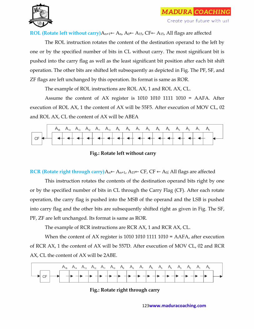
123www.maduracoaching.com
ROL (Rotate left without carry)An+1← An, A0← A15, CF← A15, All flags are affected
The ROL instruction rotates the content of the destination operand to the left by
one or by the specified number of bits in CL without carry. The most significant bit is
pushed into the carry flag as well as the least significant bit position after each bit shift
operation. The other bits are shifted left subsequently as depicted in Fig. The PF, SF, and
ZF flags are left unchanged by this operation. Its format is same as ROR.
The example of ROL instructions are ROL AX, 1 and ROL AX, CL.
Assume the content of AX register is 1010 1010 1111 1010 = AAFA. After
execution of ROL AX, 1 the content of AX will be 55F5. After execution of MOV CL, 02
and ROL AX, CL the content of AX will be ABEA
Fig.: Rotate left without carry
RCR (Rotate right through carry) An← An+1, A15← CF, CF ← A0; All flags are affected
This instruction rotates the contents of the destination operand bits right by one
or by the specified number of bits in CL through the Carry Flag (CF). After each rotate
operation, the carry flag is pushed into the MSB of the operand and the LSB is pushed
into carry flag and the other bits are subsequently shifted right as given in Fig. The SF,
PF, ZF are left unchanged. Its format is same as ROR.
The example of RCR instructions are RCR AX, 1 and RCR AX, CL.
When the content of AX register is 1010 1010 1111 1010 = AAFA, after execution
of RCR AX, 1 the content of AX will be 557D. After execution of MOV CL, 02 and RCR
AX, CL the content of AX will be 2ABE.
Fig.: Rotate right through carry

124www.maduracoaching.com
RCL (Rotate left Through Carry) An+1← An, CF ← A15, A0← CF All flags are affected
The RCL instruction rotates the contents of the destination operand left by one or
by the specified number of bits in CL through Carry Flag (CF). After each rotate
operation, the carry flag is pushed into LSB and the MSB of the operand is pushed into
carry flag. The remaining bits are subsequently shifted left as shown in Fig. The SF, PF,
ZF are left unchanged.
The example of RCL instructions are RCL AX, 1 and RCL AX, CL.
Fig.: Rotate left through carry
When the content of AX register is 1010 1010 1111 1010 = AAFA, after execution
of RCL AX, 1 the content of AX will be 55F4. After execution of MOV CL, 02 and RCL
AX, CL the content of AX will be ABE9.
Jump Instructions
The jump instructions are generally used to change the sequence of the program
execution. There are two types of jump instructions, namely, conditional and
unconditional. The conditional jump instructions transfer the program to the specified
address when condition is satisfied only. The unconditional jump instructions transfer
the program to the specified address unconditionally. All conditional and unconditional
jump instructions are discussed in this section.
JMP target (Unconditional jump to target)
This jump instruction unconditionally transfers the control of execution to the
specified address using an 8-bit or 16-bit displacement or CS: IP. After execution of this
instruction, no flags are affected. The jump instructions have different formats to
specify the jump address.
Sort: IP ← (IP + (target displacement sign-extended))

125www.maduracoaching.com
Near: IP ← (IP + (target displacement))
Indirect: IP ← (register or value in memory)
Far: CS ← targ_seg;
IP ← targ_offset, AX← (AL * source 8)
Flag affected: None
Short jumps are within ±128 bytes of JMP instruction–only IP is affected.
Near jumps are within same segment–only IP is affected. Near jump allows a
jump within ±32 KB
Indirect jumps are within the same segment–only IP is affected.
Far jumps are to a different segment–both CS and IP are affected.
JCXZ Target (short) (Jump short if CX register is 0) Flag affected: None
The object codes of JCXZ jump on CX zero instructions are
1110 0011 disp
Jcond (Jump on condition) IP ← (IP+(8-bit displacement sign-extended to 16 bits)), Flag
affected: None
If conditional jump instructions are executed, program control can be transferred
to the address specified by instruction itself. If the condition is not satisfied, instructions
are executed sequentially. Here, condition is the status of flag. After execution of these
instructions, no flags are affected. The address will be specified in the instruction which
will be varied from-80H (-128) bytes to 7FH(127) bytes. Therefore, only short jumps can
be implemented using conditional branch instructions. The conditions of jump
instructions are given in Table.
Table: Conditional JUMP instructions

126www.maduracoaching.com
Loop Instructions
The LOOP instruction executes the part of the program from the level or address
specified in the instruction up to the loop instruction, CX number of times. After each
iteration, CX is decremented automatically. If the content of CX is not zero, the LOOP
instruction transfers control to starting address of the LOOP for execution. If CX is zero,
the execution of LOOP instruction is completed and then the next instruction of the
program will be executed. The LOOP instruction can be explained with an example as
follows:
LEA SI, 0100; Load SI with source address of data
LEA DI, 0200; Load DI with destination address of data
MOV CX, 0009; Number of bytes 9 is loaded in CX register
START LODSB; Data byte to AL and increment SI by 1
STOSB; The content of AL is stored in destination address
represented by DI and and increment DI by 1
LOOP START; repeat until CX = 0
The above example shows how a string of bytes can be shifted from one memory
block specified by SI to other memory block specified by DI using LOOP instructions.

127www.maduracoaching.com
The LODSB instruction is equivalent to
MOV AL, [SI]
INC SI
The STOSB instruction is equivalent to
MOV [DI], AL
INC DI
And the LOOP instruction is equivalent to
DEC CX
JNZ START
In this case, LODSB and STOSB instructions are executed 9 times and a block of
9-byte data will be copied from source memory to destination memory sequentially.
LOOP Target (short) (Loop to short target) CX ← (CX-1); Jump if CX ! = 0 . The CX
register is decremented by 1. If CX now is not equal to 0, the loop is back to target.
Otherwise, continue.
LOOPE/Z Target (short) (Loop to short target if Z bit set)CX ← (CX-1); jump if CX! = 0
and ZF = 1. The CX register is decremented by 1. If CX is not equal to 0 or if the Z bit is
set, the loop is back to short target.
LOOPNE / NZ(Loop to short target if Z bit is clear)CX ← (CX-1); jump if CX! = 0 and
ZF = 0
The CX register is decremented by 1. If CX is not equal to 0 or if the Z bit is clear,
the loop is back to short target.
CALL and RETURN Instructions
The CALL and RET (return) instructions are used to call a subroutine or a
procedure that can be executed several times from a main program. The starting
address of the subroutine or procedure can be specified directly or indirectly depending
upon the addressing mode. There are two types of procedures, namely,
intrasegmentand intersegment. The subroutine within a segment is known as

128www.maduracoaching.com
intrasegment subroutine or NEARCALL. The subroutine from one segment to another
segment is known as intersegment subroutine or FARCALL. These instructions are
unconditional branch instructions. After execution of these instructions, the
incremented IP and CS are stored onto the stack and loads the CS and IP registers with
the segment and offset addresses of the procedure to be called. For NEAR CALL, only
the IP register is stored on stack. But for FARCALL, both IP and CS are stored onto the
stack. Hence the NEAR and FAR CALLs can be discriminated using opcode. The
operation of CALL and RET instructions are explained below:
CALL target (Call a procedure) Near call: PUSH IP, JMP to target
SP← IP, SP← SP-2, IP← IP + DISP
Far call: PUSH CS, PUSH IP, JMP to target :Flag affected: None
SP← CS, SP← SP-2, SP← IP, SP← SP-2, IP← 16 bit DATA
CS← 16-bit DATA
The syntax for a near call (same segment) is CALL target.
The syntax for a far call (different segment) is CALL FAR target.
RET (Return from procedure)
RET n (return from procedure and add n to SP)
Near return: POP IP
IP← SP, SP← SP + 2
The syntax for a near return is RET.
Far return: POP IP, POP CS; Flag affected: None
IP← SP, SP← SP + 2, CS← SP, SP← SP + DISP
The syntax for a far return is RET FAR.
During execution of CALL instruction, initially the IP and CS of the next
instruction is pushed onto stack, then the control is transferred to the procedure. At the
end of execution of procedure, RET instruction must be executed. When RET instruction
is executed, the previously stored content of IP and CS along with flags are retrieved
into CS, IP and flag registers from the stack respectively. After that the execution of the

129www.maduracoaching.com
main program again starts. Usually, the procedures are two types, namely, a near
procedure or a far procedure. While in case of NEAR procedure, the current contents of
SP points to IP but for a FAR procedure, the current contents of SP points to IP and CS
at the time of return. Actually, the RET instructions are of four types such as
Return within segment
Return within segment adding 16-bit immediate displacement to the SP contents
Return intersegment
Return intersegment adding 16-bit immediate displacement to the SP contents
INT n (Interrupt (software))
PUSHF; IF← 0; TF← 0; PUSH CS; PUSH IP
IP← 0000: [type * 4];
CS← 0000: [(type * 4) + 2]; Flag affected: IT
INT n is a software interrupt to be serviced. The flags and current CS: IP are
pushed onto the stack. The CS: IP stored in the vector indicated by the interrupt number
are then loaded and the next instruction is fetched from that interrupt service routine
address. There are 256 interrupts corresponding to the types from00H to FFH in the
interrupt structure of 8086. When an INT n instruction is executed, the TYPE byte n is
multiplied by 4 and the contents of IP and CS of the interrupt service routine will be
taken from the hexadecimal multiplication (n × 4) as offset address and 0000 as segment
address.
INTO (Interrupt on overflow)
If OF = 1, then perform INT through vector 4; Flag affected: None
Interrupts the system if the overflow bit is set following a mathematical
instruction. This indicates a carry from a signed value.
This instruction is executed, when the overflow flag OF is set. The new contents
of IP and CS are taken from the address 0000: 0010 as explained in INT type instruction.
This is equivalent to a type 4 interrupt instruction.

130www.maduracoaching.com
IRET (Return from interrupt service routine)
POP IP; POP CS; POPF AX (AL * src8); Flag affected: All
When an interrupt service routine is to be called, before transferring control to it,
the IP, CS and flag register are stored on to stack to indicate the location from where the
execution is to be continued after the ISR is executed. This instruction appears at the
bottom of all Interrupt Service Routines (ISR).
When IRET is executed, the values of IP, CS and flags are retrieved from the
stack to continue the execution of the main program.
String Instructions
Usually, a series of data bytes is known as a string of bytes and a series of data
words is known as a string of words. For moving a string of bytes or words, 8086/8088
processors have five instructions such as STOS (store string byte or word), LODS (load
string byte or word), MOVS (move string byte or word), SCAS (scan string byte or
word) and CMPS (compare string byte or word). For these instructions, a source of
string byte or word is DS : SI and destination of string byte or word is ES : SI. After
execution of these instructions, the offset memory pointer SI and DI are incremented or
decremented by one or two depending upon direction flag. In this section STOS, LODS,
MOVS, SCAS and CMPS are explained.
MOVSB (Move string byte) ES: [DI] ← DS: [SI]; DI = DI ± 1; SI = SI ± 1; Flag affected:
None.
Moves a string a byte at a time from source memory DS : SI to destination
memory ES: DI. SI and DI are incremented or decremented by 1, depending on
Direction Flag(DF).
The object code of MOVSB is 1010010w = A4 as w = 0.
MOVSW (Move string word) ES: [DI] ← DS: [SI]; DI = DI ± 2; SI = SI ± 2; Flag affected:
None
131www.maduracoaching.com
Moves a string a word at a time from source memory DS: SI to destination
memory ES: DI. SI and DI are incremented or decremented by 2, depending on
Direction Flag (DF).
STOSB (Store string byte) ES: [DI] ← AL; DI = DI ± 1; Flag affected: None
Moves a string one byte at a time from AL to destination memory address ES: DI.
DI is then incremented or decremented by 1, depending on Direction Flag (DF).
STOSW (Store string word) ES: [DI] ← AX; DI = DI±2; Flag affected: None
Moves a string one word at a time from AX to destination memory address ES:
DI. DI is then incremented or decremented by 2, depending on Direction Flag (DF). The
object code of STOSW is 1010 101w = AB as w = 1.
LODSB (Load string byte) AL ← DS: [SI]; SI = SI ± 1; Flag affected: None
Moves a string one byte at a time from source memory address DS: SI to AL.
Then SI is incremented or decremented by 1, depending on Direction Flag (DF).
LODSW (Load string word) AX ← DS: [SI]; SI = SI ± 2; Flag affected: None
Moves a string one word at a time from source memory address DS: SI to AX.
Then SI is incremented or decremented by 2, depending on Direction Flag (DF). The
object code of LODSW is 1010 110w = AD as w = 1.
CMPSB (Compare string byte) Flags← (result of CMP DS: [SI], ES: [DI]); DI = DI±1; SI
=SI±1; Flag affected: as CMP
The byte or 8-bit data at DS: SI is compared with the byte or 8-bit data at ES:DI
and the flags are set accordingly. Both SI and DI are incremented or decremented by 1,
depending on the Direction Flag (DF).This instruction is combined with a REP prefix, so
that we can compare two strings and we can also find at what point two strings no
longer are equal.
CMPSW (Compare string word)Flags← (result of CMP DS: [SI], ES: [DI]); DI = DI ± 2;
SI= SI ± 2; Flag affected: as CMP
The word or 16-bit data at DS: SI is compared with the word or 16-bit data at ES:
DI and the flags are set accordingly. Both SI and DI are incremented or decremented by
2, depending on the Direction Flag (DF).This instruction is combined with REP prefix,
132www.maduracoaching.com
so that we can compare two strings and we can also locate at what point two strings no
longer are equal.
SCASB (Scan string byte) Flags ← (result of CMP ES: [DI], AL); DI = DI ± 1; Flag
affected: same as CMP instruction
The byte or 8-bit data at ES: DI is compared to the contents of AL and
correspondingly flags are set. DI is incremented or decremented by 1 depending upon
the Direction Flag (DF). The SCASB can be combined with a REP prefix, so that we can
be able to scan a string looking for the first occurrence of a particular byte.
SCASW (Scan string word) Flags ← (result of CMP ES: [DI], AX); DI = DI ± 2; Flag
affected: same as CMP instruction
The word or 16-bit data at ES: DI is compared to the contents of AX and
correspondingly flags are set and correspondingly flags are set. DI is incremented or
decremented by 2 depending upon the Direction Flag (DF). The SCASW can be
combined with a REP prefix, so that we can be able to scan a string looking for the first
occurrence of a particular word.
REPEAT Instructions:
The string instructions are used to operate on large blocks of data. To refer a
string, two parameters are required such as (i) starting/end address of the string, and
(ii) length of the string. Usually starting/end address of the string is represented by DS:
SI and the length of a string is stored as count in the CX register. After each iteration,
the incrementing or decrementing of the pointer (SI or DI) depends upon the direction
flag (DF) and the counter is decremented by one. To perform the string instructions
repeatedly, REP (repeat) instructions are used. Hence the string instruction with the
REP prefix is executed repeatedly until the CX register becomes zero. If CX becomes
zero, the execution proceeds to the next instruction in sequence. The most commonly
used REP instructions are REP (repeat), REPE (repeat while equal), REPZ (repeat while
zero), REPNE (repeat while not equal), and REPNZ (repeat while not zero)which are
explained below.
133www.maduracoaching.com
REP / REPE / REPZ (Repeat string instruction (prefix) CX← (CX-1); until CX = 0;Flag
affected: Z
This is a prefix byte that forces a string operation to be repeated as long as CX is
not equal to 0. CX is decremented once for each repetition.
REPNE / REPNZ (Repeat string instruction while not zero (prefix)) ZF← 0; CX ← (CX-
1); String Operation repeats while (CX! = 0 and ZF! = 0); Flag affected: Z. This is a prefix
bytethat keeps a string operation repeating while CX is not zero and Z! = 0.
Processor Control Instructions
These instructions control the operation of processor and set or clear the status
indicators. These instructions are classified into two types such as flag-manipulation
instructions and machine-control instructions. The flag-manipulation instructions
directly change some flags of the 8086 processor but the machine-control instructions
control the system bus functions.
The Carry (CF), Direction (DF) and Interrupt (IF) flags can be set or reset directly
and the carry flag can be inverted by these instructions. The DF and IF are processor
control bits. DF is used with the string instructions to change the content of pointer
registers. When DF = 0, pointer register (DI) is incremented. When DF = 1, the pointer
register (DI) is decremented. The STD (set direction flag) and CLD (clear direction flag)
instructions are used to set or clear this flag. The STI (set interrupt flag) and CLI (clear
interrupt flag) are used to enable or disable maskable interrupts on INTR line. When TF
(trap flag) is set, a type 1 interrupt is generated after execution of each processor
instructions. There are no specific instructions to set or reset the TF. POPF and SAHF
instructions, which are termed as data-transfer instructions are used to modify flags.
The machine-control instructions are HLT, WAIT, NOP ESC and LOCK. Some
instructions are specially used for coprocessors. There are three coprocessor instructions
as WAIT, LOCK and ESC. In this section all processor control instructions are
explained.
CLC (Clear the carry flag) CF ← 0; Flag affected: C.

134www.maduracoaching.com
The CLC instruction is used in the carry flag low. The object code of CLC
instruction is 1111 1000 = F8
CMS (Complement the carry flag)CF ← ~CF; Flag affected: C
The CMC instruction is used to complement the carry flag. The object code of CMC
instruction is 1111 0101 = F5
STC (Set the carry flag): CF ← 1; Flag affected: C
The CMC instruction is used to set the carry flag. The object code of STC
instruction is 1111 1001 = F9
CLD (Clear direction flag) DF ← 0; Flag affected: D
Clear direction flag to 0. When DF = 0, pointer register (SI or DI) is automatically
incremented by 1.
The object code of CLD instruction is 1111 1100 = FC
STD (Set direction flag)DF ← 1; Flag affected: D
Sets direction flag to 1. When DF = 1, pointer register (SI or DI) is automatically
decremented by 1.
The object code of STD instruction is 1111 1101 = FD
CLI (Clear interrupt flag) IF ← 0; Flag affected: IF
Clears the interrupt enable flag which disables interrupts.
The object code of CLI instruction is 1111 1010 = FA
STI (Set interrupt flag) IF←1; Flag affected: IF
Sets the interrupt enable flag which enables interrupts.
The object code of STI instruction is 1111 1011 = FB
HLT (Halt) Flag affected: None.
Halt instruction is used to ask the processor to stop execution. Actually, it hangs
the processor in a series of self-inflicted NOP’s until an interrupt occurs.
The object code of HLT instruction is 1111 0100 = F4
WAIT (Wait)Flag affected: None.
It causes the processor to wait for a completion signal from the coprocessor.
The object code of WAIT instruction is 1001 1011 = 9B

135www.maduracoaching.com
LOCK (Lock bus)Flag affected: None.
This instruction is used to avoid any other processors. Actually, it locks the bus
attached to LOCK pin of device while a multi-cycle instruction completes.
The object code of LOCK instruction is 1111 0000 = F0
NOP (No operation):When NOP instruction is executed, this instruction does not allow
the processor to perform any operation except for incrementing the IP by one.
The object code of NOP instruction is 1001 0000 = 90
TEST: The TEST input is examined by a WAIT instruction. When the WAIT instruction
is executed, it holds the operation of the processor with the current status till the logic
level on the TEST pin is low. Therefore, the processor remains in idle state and the TEST
pin goes low.
ESC (Escape):The ESC instruction is used as a prefix to the coprocessor instructions.
The 8086 processor puts the source operand on the data bus but no operation further
takes place. The coprocessor continuously examined the data bus content and it is
activated by ESC instruction and it reads two operands and thereafter starts execution.