microprocessor and peripherals
TRANSCRIPT
MGM‟SJawaharlalNehruEngineeringCollege
Laboratory Manual
MICROPROCESSOR ANDPERIPHERALS
For
TE (ECT)
Vishwashri Kulkarni
Author JNEC, Aurangabad
MGM’S
Jawaharlal Nehru Engineering CollegeN-6, CIDCO, Aurangabad
Department of Electronics &TelecommunicationVision of the Department:
To develop GREAT technocrats and to establish centre of excellence in the field of Electronics and
Telecommunications.
} Global technocrats with human values
} Research and lifelong learning attitude,
} Excellent ability to tackle challenges
} Awareness of the needs of society
} Technical expertise
Mission of the Department:
1. To provide good technical education and enhance technical competency by providing good infrastructure,
resources, effective teaching learning process and competent, caring and committed faculty.
2. To provide various platforms to students for cultivating professional attitude and ethical values.
3. Creating a strong foundation among students which will enable them to pursue their career choice.
MGM’s Jawaharlal Nehru Engineering College 2015
PREFACE
It is my great pleasure to present this laboratory manual for third year Electronics students for the subject of Microprocessor and peripherals (MPP).
Microprocessor is the brain of computer. It is a general purpose programmable logic device. A thorough understanding of 8085Microprocessor concepts, demands Assembly Language programming with in depth knowledge of instructions and clarity in analysis of the task.
Most of the students find it difficult to start with the programming assignment. Therefore, a structured approach to learn programming through steps like problem statement, analysis, logic & flowchart, actual program (Mnemonics)and comments, is illustrated with sample programs.
This lab manual introduces students to the elementary programming techniques, interfacing and designing simple applications using peripheral chips like 8255, 8279, 8253etc.
Students are advised to thoroughly go through this manual rather than only topics mentioned in the syllabus, as practical aspects are the key to understanding and conceptual visualization of theoretical aspects covered in the books.
Good Luck for your Enjoyable Laboratory Sessions.
Author
2
MGM’s Jawaharlal Nehru Engineering College 2015
SUBJECTINDEX
I Do‟s and Don‟ts.
II Lab exercises.
PART A
Introduction to 8085 kit
PART B
1. Data manipulation programs.
1.1 Arithmetic operation on two 8 Bit numbers.
1.2 Arithmetic operation on two 16 Bit numbers .
1.3 Operation on two 16 Bit BCD numbers using DAA instruction .
1.4 Data Transfer Programs(Block Transfer) .
1.5 To find minimum and maximum number in a block of data
1.6 Addition of series.
1.7 Sorting in Ascending order.
1.8 Sorting in Descending order.
1.9 Multiplication of 8 bit numbers.
2. Code conversion programs.
3. ADC interface with 8255.
4. DAC interface with 8255.
5. Study of 8255(Relay I/F].
6. Study of 8255(LED I/F).
7. Stepper motor interface with 8255.
8. Study of 8253.
9. Study of 8259.
III. Quiz on the subject.
IV. Conduction Viva-Voce Examination.
V. Evaluation and Marking Systems.
3

MGM’s Jawaharlal Nehru Engineering College 2015
DO‟s andDON‟T‟sinLaboratory:
1. Do not handle any kit before reading the instructions/Instruction manuals.
2. Use correct power supply with the proper kit.
3. Do not forcefully place connectors to avoid the damage.
4. Strictly observe the instructions given by the teacher/Lab Instructor.
InstructionforLaboratoryTeachers:
1. Lab work completed during prior session should be corrected during the next lab session.
2. Students should be guided and helped whenever they face difficulties.
3. The promptness of submission should be encouraged by way of marking and evaluation patterns that will benefit the sincere students.
4
MGM’s Jawaharlal Nehru Engineering College 2015
1.LabExercises:[Purpose of these exercises is to introduce the students to Assembly Language Programming for 8085, types of peripheral chips, their interfacing & programming.
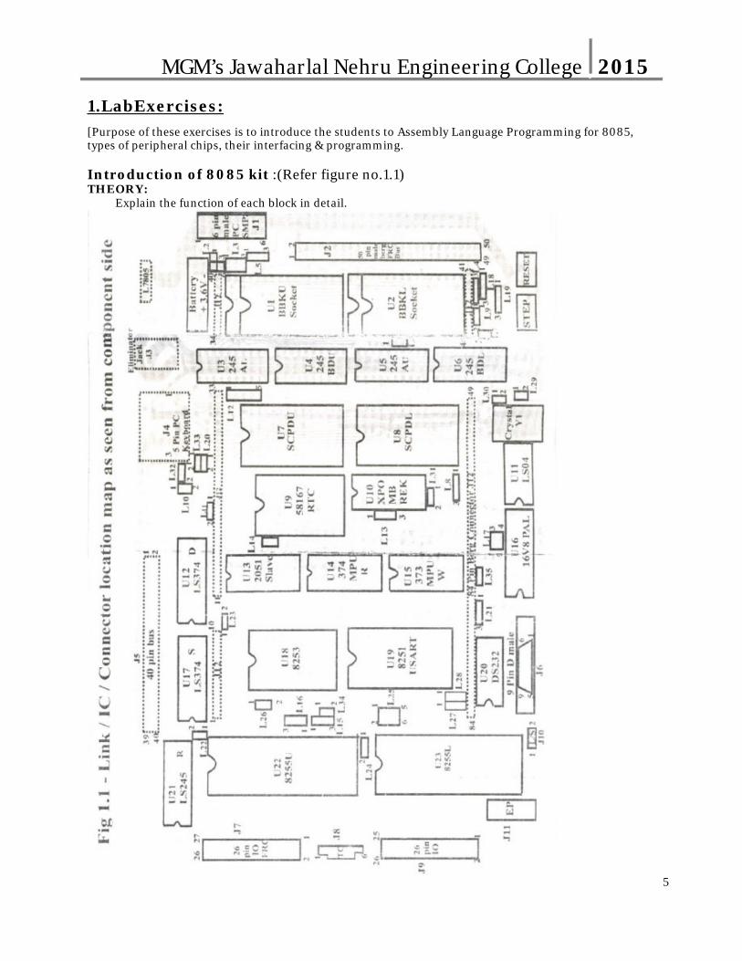
Introduction of 8085 kit :(Refer figure no.1.1)THEORY:
Explain the function of each block in detail.
5

MGM’s Jawaharlal Nehru Engineering College 2015
Exercise No.1: Data manipulation program:
Exercise No.1.1 : Arithmetic operation on two 8 bit numbers.
a) Addition of two 8 bit numbers.
Aim : To write assembly language program for addition of two 8 bit numbers.
Statement: Add two 8 bit numbers ,where first no. is present in memory location 2400 and second no. in2401.Store result in memory location 2402.
Algorithm:1. Initialize HL pair to point to the memory location of first no.2. Transfer the first no. to Register A.3. Increment HL pair to point to the next no.4. Add contents of the memory location pointed by HL pair and the contents of register A.5. Store the result in the mentioned memory location.6. Stop.
Sample program:
Memory Opcode/data/ label Mnemonics CommentsAddress address7000,01,02 21,00,24 LXIH,2400 H Initialize HL pair7003 7E MOV A, M Transfer first no. to reg A7004 23 INX H Increment HL pair
7005 86 ADD M Add the two nos.7006,07,08 32,02,24 STA2402 H Store the result in 2403H7009 CF RST1 stop
Data: 2400H=11H and 2401H=12H
Result: 2402H=23 H
Conclusion: Thus, the program written for addition of two 8 bit numbers is successfully executed.
6

MGM’s Jawaharlal Nehru Engineering College 2015b) Subtraction of two 8 bit numbers.
Aim: To write assembly language program for Subtraction of two 8 bit numbers.
Statement: Subtract two 8 bit numbers. Subtract the second no.present in memory location 2401H from thefirst no. present in memory location 2400H and Store result in memory location 2402H.
Algorithm:1. Initialize HL pair to point to the memory location of first no.2. Transfer the first no. to Register A.3. Increment HL pair to point to the next no.4. Subtract the contents of the memory location pointed by HL pair from contents of register A.5. Store the result in the mentioned memory location.6. Stop.
Sample Program:
Memory Opcode/data/ label Mnemonics CommentsAddress address7000,01,02 21,00,24 LXIH,2400 H Initialize HL pair7003 7E MOV A, M Transfer first no. to reg A7004 23 INX H Increment HL pair
7005 96 SUB M Add the two nos.7006,07,08 32,02,24 STA2402 H Store the result in 2402H7009 CF RST1 stop
Data: 2400H=05H and 2401H=02H
Result: 2403H=03 H
Conclusion: Thus program written for Subtraction of two 8 bit numbers is successfully executed.
7
MGM’s Jawaharlal Nehru Engineering College 2015
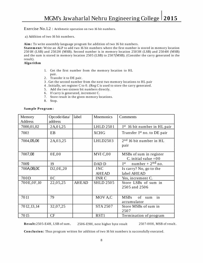
Exercise No.1.2 : Arithmetic operation on two 16 bit numbers.
a) Addition of two 16 bit numbers.
Aim: To write assembly language program for addition of two 16 bit numbers.Statement: Write an ALP to add two 16 bit numbers where the first number is stored in memory location 2501H (LSB) and 2502H (MSB). Second number is in memory location 2503H (LSB) and 2504H (MSB) and the sum is stored in memory location 2505 (LSB) to 2507(MSB). (Consider the carry generated in the result).Algorithm
1. Get the first number from the memory location to HL pair.
2. Transfer it to DE pair.3 . Get the second number from the next two memory locations to HL pair 4 . Initially, set register C to 0. (Reg C is used to store the carry generated.5. Add the two sixteen bit numbers directly.6. If carry is generated, increment C.7. Store result in the given memory locations.8. Stop.
Sample Program:
Memory Opcode/data/ label Mnemonics CommentsAddress address7000,01,02 2A,01,25 LHLD 2501 1st 16 bit number in HL pair
7003 EB XCHG Transfer 1st no. to DE pair
7004,05,06 2A,03,25 LHLD2503 2nd 16 bit number in HLpair
7007,08 0E,00 MVI C,00 MSBs of sum in registerC. initial value =00
7009 19 DAD D 1st number + 2nd no.700A,0B,0C D2,0E,20 JNC Is carry? No, go to the
AHEAD label AHEAD700D 0C INR C Yes, increment C.700E,0F,10 22,05,25 AHEAD SHLD 2505 Store LSBs of sum in
2505 and 2506
7011 79 MOV A,C MSBs of sum inaccumulator
7012,13,14 32,07,25 STA 2507 Store MSBs of sum in2507
7015 CF RST1 Termination of program
Result:2505-E4H, LSB of sum. 2506-E9H, next higher byte result 2507-00H, MSB of result.
Conclusion: Thus program written for addition of two 16 bit numbers is successfully executed.
8

MGM’s Jawaharlal Nehru Engineering College 2015b) Subtraction of two 16 bit numbers.
Aim: To write assembly language program for Subtraction of two 16 bit numbers
Statement: Two 16 bit numbers are stored from memory location. Subtract number stored at 2501H(LSB) & 2502H (MSB) from the 16 Bit number stored at 2503 (LSB) & 2504H (MSB).Store result at 2506H (LSB) & 2507H (MSB).
Algorithm:1. Transfer the first number from the memory location to HL pair.2. Transfer it to DE pair.3. Load second 16 bit number from the next two memory locations in HL pair.4. Subtract lower byte of 2nd number5. Store result in L register.6. Subtract higher byte of second number with borrow.7. Store result in H register.8. Stop
Sample Program:
Memory Opcode/data/ label Mnemonics CommentsAddress address
7000,01,02 2A,01,25 LHLD 2501 1st 16 bit number in HL pair
7003 EB XCHG Transfer 1st no. to DE pair
7004,05,06 2A,03,25 LHLD2503 2nd 16 bit number in HL pair
7007 7B MOV A,E Get lower byte of 1number.
7008 95 SUB L Subtract lower byte of 2number
7009 6F MOV L,A Store the result in L register700A 7A MOV A,D Get higher byte of 1
number700B 9C SBB H Subtract higher byte of 2
number with borrow
7000C 67 MOV H,A Store result in H register700D,0E,0F 22,05,25 SHLD 2505 Store result at 2505H/2506H7010 CF RST1 Stop
Data: 2501H = 19H2502H = 6AH 2503H = 15H 2504H = 5CH
Result: 6A19 H-5C15 H = 0E04 H2505H = 04H2506H = 0EH
Conclusion: Thus program written for Subtraction of two 16 bit numbers is successfully executed.
9
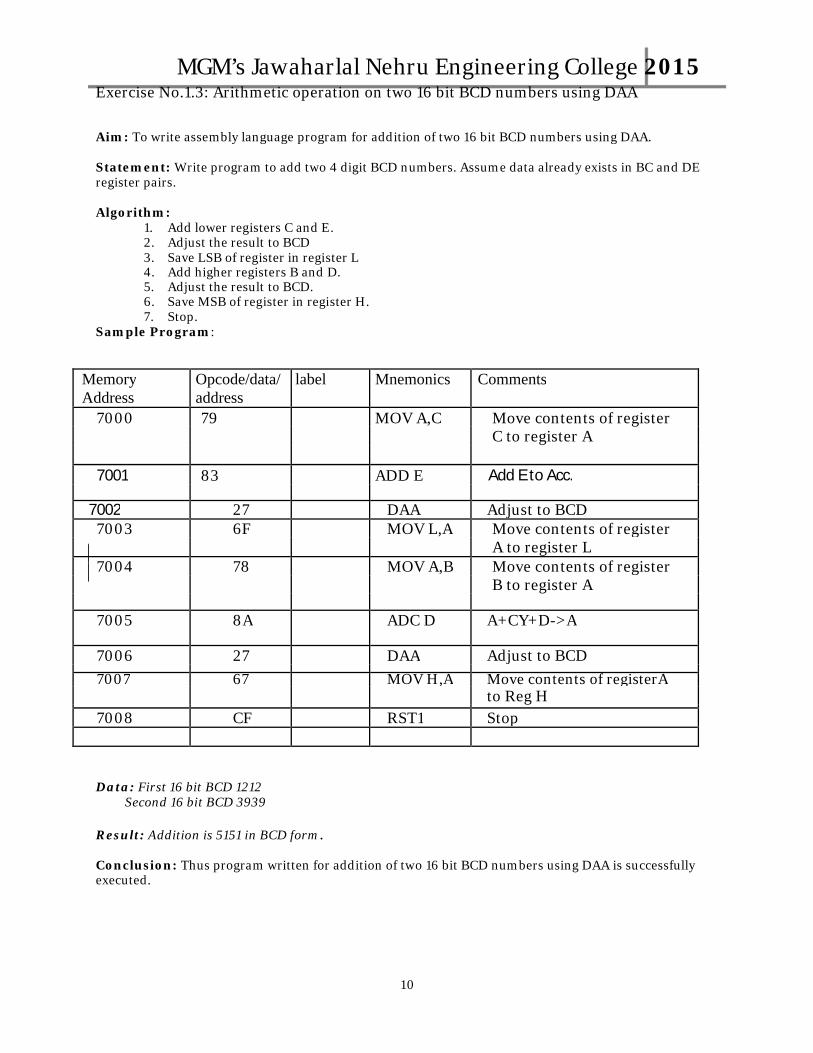
MGM’s Jawaharlal Nehru Engineering College 2015Exercise No.1.3: Arithmetic operation on two 16 bit BCD numbers using DAA
Aim: To write assembly language program for addition of two 16 bit BCD numbers using DAA.
Statement: Write program to add two 4 digit BCD numbers. Assume data already exists in BC and DEregister pairs.
Algorithm:1. Add lower registers C and E.2. Adjust the result to BCD3. Save LSB of register in register L4. Add higher registers B and D.5. Adjust the result to BCD.6. Save MSB of register in register H.7. Stop.
Sample Program:
Memory Opcode/data/ label Mnemonics CommentsAddress address
7000 79 MOV A,C Move contents of registerC to register A
7001 83 ADD E Add E to Acc.
7002 27 DAA Adjust to BCD7003 6F MOV L,A Move contents of register
A to register L7004 78 MOV A,B Move contents of register
B to register A
7005 8A ADC D A+CY+D->A
7006 27 DAA Adjust to BCD
7007 67 MOV H,A Move contents of registerAto Reg H
7008 CF RST1 Stop
Data: First 16 bit BCD 1212Second 16 bit BCD 3939
Result: Addition is 5151 in BCD form.
Conclusion: Thus program written for addition of two 16 bit BCD numbers using DAA is successfullyexecuted.
10

MGM’s Jawaharlal Nehru Engineering College 2015
Exercise No.1.4: Data transfer programs:
Aim: To write data transfer array programs and execute.
Statement: 5 no. of bytes is stored from the memory locations 2201h. Transfer the entire block of data bytes from 2201H to 2301H onwards.
Algorithm (Logic):1.Initialize the source memory pointer.2. Initialize the destination memory pointer.3. Initialize the counter with 5.4. Move the contents of the source memory to accumulator.5. Do whatever manipulation is specified /required.6. Transfer the accumulator contents to destination memory location.7. Increment source, destination memory pointer and decrement the counter.8. If the count is not zero, jump back to step 4.9. If the count is zero, stop.
Sample:N=5 bytes, source location: 2201 to 2205, destination location: 2301 to 2305.Data Transfer:
Memory Opcode/data/ad label Mnemonics CommentsAddress dr7000,01,02 21,01,22 LXI H,2201H Initialize HL pair with
source (src) memory.7003,04,05 01,01,23 LXI B,2301H Initialize BC pair with
destination (destn) memory.7006,07 16,05 MVI D,05H Initialize D with count=057008 7E LOOP MOV A,M Transfer src data to
accumulator (acc).7009 02 STAX B Transfer acc contents to
destn.700A 23 INX H Increment HLpair by 1700B 03 INX B Increment BC pair by1700C 15 DCRD Decrement D by1700D,0E,0F C2,08,70 JNZ LOOP Jump to loop if Zero flag is
not set.7010 CF RST1 Stop
Data: 5 no. of bytes stored from 2201 onwards.
Result: Same 5 no. of bytes stored in 2301 onwards
Conclusion: Thus program written for data transfer is successfully executed.
11
MGM’s Jawaharlal Nehru Engineering College 2015
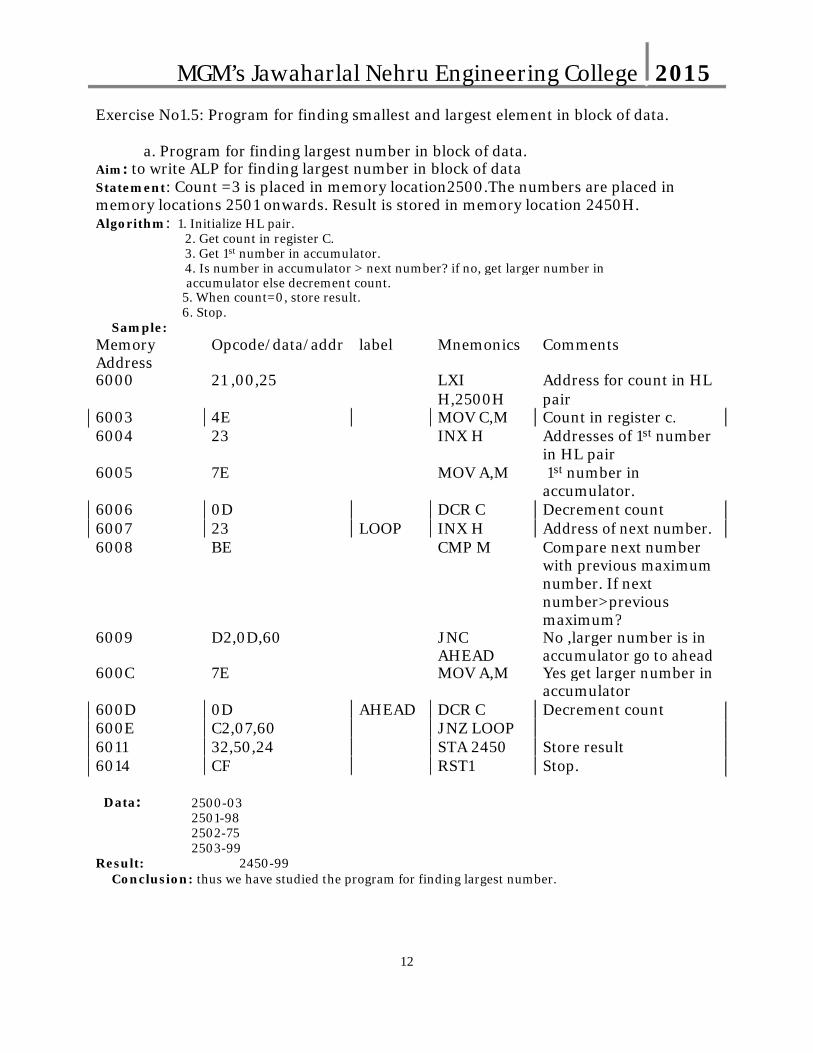
Exercise No1.5: Program for finding smallest and largest element in block of data.
a. Program for finding largest number in block of data. Aim: to write ALP for finding largest number in block of dataStatement: Count =3 is placed in memory location2500.The numbers are placed inmemory locations 2501 onwards. Result is stored in memory location 2450H.Algorithm: 1. Initialize HL pair.
2. Get count in register C.3. Get 1st number in accumulator.4. Is number in accumulator > next number? if no, get larger number inaccumulator else decrement count.
5. When count=0, store result.6. Stop.
Sample:Memory Opcode/data/addr label Mnemonics CommentsAddress6000 21 ,00,25 LXI Address for count in HL
H,2500H pair6003 4E MOV C,M Count in register c.6004 23 INX H Addresses of 1st number
in HL pair6005 7E MOV A,M 1st number in
accumulator.6006 0D DCR C Decrement count6007 23 LOOP INX H Address of next number.6008 BE CMP M Compare next number
with previous maximumnumber. If nextnumber>previousmaximum?
6009 D2,0D,60 JNC No ,larger number is inAHEAD accumulator go to ahead
600C 7E MOV A,M Yes get larger number inaccumulator
600D 0D AHEAD DCR C Decrement count600E C2,07,60 JNZ LOOP6011 32,50,24 STA 2450 Store result6014 CF RST1 Stop.
Data: 2500-032501-982502-752503-99
Result: 2450-99Conclusion: thus we have studied the program for finding largest number.
12
MGM’s Jawaharlal Nehru Engineering College 2015
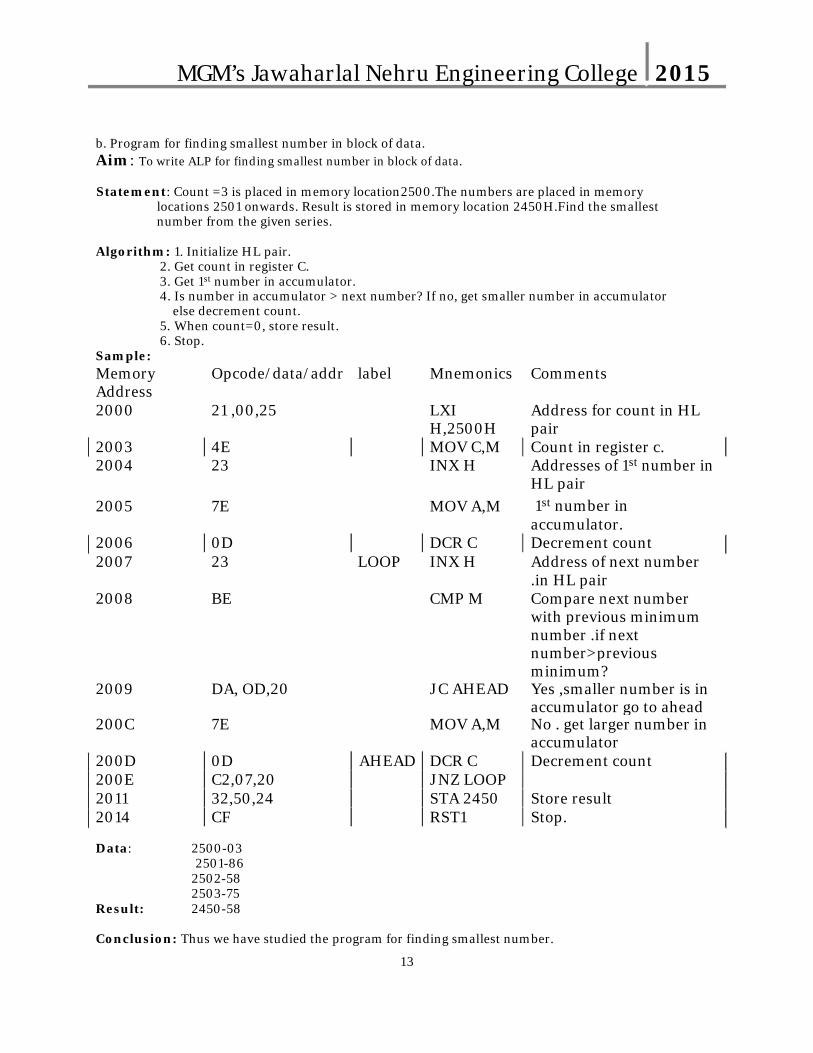
b. Program for finding smallest number in block of data.Aim: To write ALP for finding smallest number in block of data.
Statement: Count =3 is placed in memory location2500.The numbers are placed in memory locations 2501 onwards. Result is stored in memory location 2450H.Find the smallest number from the given series.
Algorithm: 1. Initialize HL pair.2. Get count in register C.3. Get 1st number in accumulator.4. Is number in accumulator > next number? If no, get smaller number in accumulator
else decrement count.5. When count=0, store result.6. Stop.
Sample:Memory Opcode/data/addr label Mnemonics CommentsAddress2000 21 ,00,25 LXI Address for count in HL
H,2500H pair2003 4E MOV C,M Count in register c.2004 23 INX H Addresses of 1st number in
HL pair
2005 7E MOV A,M 1st number inaccumulator.
2006 0D DCR C Decrement count2007 23 LOOP INX H Address of next number
.in HL pair2008 BE CMP M Compare next number
with previous minimumnumber .if nextnumber>previousminimum?
2009 DA, OD,20 JC AHEAD Yes ,smaller number is inaccumulator go to ahead
200C 7E MOV A,M No . get larger number inaccumulator
200D 0D AHEAD DCR C Decrement count200E C2,07,20 JNZ LOOP2011 32,50,24 STA 2450 Store result2014 CF RST1 Stop.
Data: 2500-032501-86
2502-582503-75
Result: 2450-58
Conclusion: Thus we have studied the program for finding smallest number.
13
MGM’s Jawaharlal Nehru Engineering College 2015
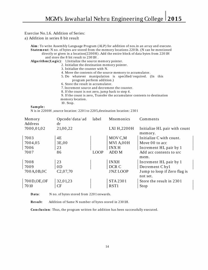
Exercise No.1.6. Addition of Series: a) Addition in series 8 bit result
Aim: To write Assembly Language Program (ALP) for addition of nos.in an array and execute.Statement: N no. of bytes are stored from the memory locations 2201h. (N can be mentioned
directly or given in a location(2200H) .Add the entire block of data bytes from 2201H and store the 8 bit result to 2301H .
Algorithm(Logic): 1.Initialize the source memory pointer.2. Initialize the destination memory pointer.3. Initialize the counter with N.4. Move the contents of the source memory to accumulator.5. Do whatever manipulation is specified/required. (In this
program perform addition.)6. Store the result in accumulator.7. Increment source and decrement the counter.8. If the count is not zero, jump back to step 4.9. If the count is zero, Transfer the accumulator contents to destination memory location.10. Stop.
Sample:N is in 2200H ,source location: 2201 to 2205,destination location: 2301
Memory Opcode/data/ad label Mnemonics CommentsAddress dr7000,01,02 21,00,22 LXI H,2200H Initialize HL pair with count
memory.7003 4E MOV C,M Initialize C with count.7004,05 3E,00 MVI A,00H Move 00 to acc7006 23 INX H Increment HL pair by 17007 86 LOOP ADD M Add acc contents to src
mem.7008 23 INXH Increment HL pair by 17009 0D DCR C Decrement C by1700A,0B,0C C2,07,70 JNZ LOOP Jump to loop if Zero flag is
not set.700D,OE,OF 32,01,23 STA 2301 Store the result in 23017010 CF RST1 Stop
Data: N no. of bytes stored from 2201 onwards.
Result: Addition of Same N number of bytes stored in 2301H.
Conclusion: Thus, the program written for addition has been successfully executed.
14
MGM’s Jawaharlal Nehru Engineering College 2015
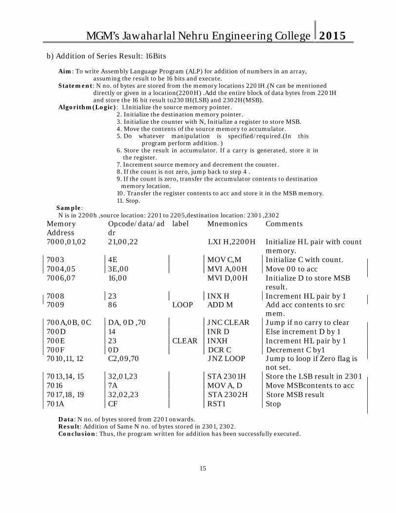
b) Addition of Series Result: 16Bits
Aim: To write Assembly Language Program (ALP) for addition of numbers in an array,assuming the result to be 16 bits and execute.
Statement: N no. of bytes are stored from the memory locations 2201H.(N can be mentioneddirectly or given in a location(2200H) .Add the entire block of data bytes from 2201H and store the 16 bit result to2301H(LSB) and 2302H(MSB).
Algorithm(Logic): 1.Initialize the source memory pointer.2. Initialize the destination memory pointer.3. Initialize the counter with N, Initialize a register to store MSB.4. Move the contents of the source memory to accumulator.5. Do whatever manipulation is specified/required.(In this
program perform addition. )6. Store the result in accumulator. If a carry is generated, store it in
the register.7. Increment source memory and decrement the counter.8. If the count is not zero, jump back to step 4 .9. If the count is zero, transfer the accumulator contents to destination
memory location.10. Transfer the register contents to acc and store it in the MSB memory.11. Stop.
Sample:N is in 2200h ,source location: 2201 to 2205,destination location: 2301 ,2302
Memory Opcode/data/ad label Mnemonics CommentsAddress dr7000,01,02 21,00,22 LXI H,2200H Initialize HL pair with count
memory.7003 4E MOV C,M Initialize C with count.7004,05 3E,00 MVI A,00H Move 00 to acc7006,07 16,00 MVI D,00H Initialize D to store MSB
result.7008 23 INX H Increment HL pair by 17009 86 LOOP ADD M Add acc contents to src
mem.700A,0B, 0C DA, 0D ,70 JNC CLEAR Jump if no carry to clear700D 14 INR D Else increment D by 1700E 23 CLEAR INXH Increment HL pair by 1700F 0D DCR C Decrement C by17010,11, 12 C2,09,70 JNZ LOOP Jump to loop if Zero flag is
not set.7013,14, 15 32,01,23 STA 2301H Store the LSB result in 23017016 7A MOV A, D Move MSBcontents to acc7017,18, 19 32,02,23 STA 2302H Store MSB result701A CF RST1 Stop
Data: N no. of bytes stored from 2201 onwards.Result: Addition of Same N no. of bytes stored in 2301, 2302.Conclusion: Thus, the program written for addition has been successfully executed.
15
MGM’s Jawaharlal Nehru Engineering College 2015
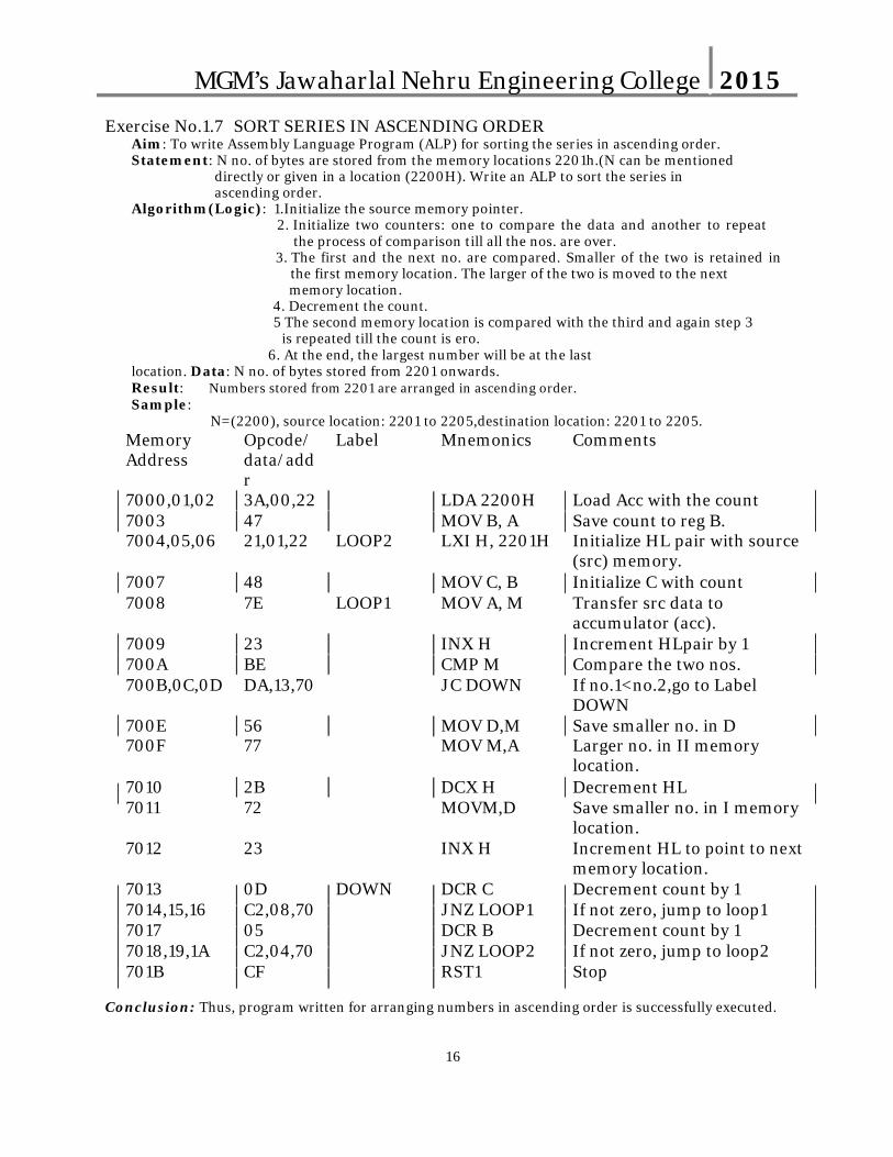
Exercise No.1.7 SORT SERIES IN ASCENDING ORDERAim: To write Assembly Language Program (ALP) for sorting the series in ascending order.Statement: N no. of bytes are stored from the memory locations 2201h.(N can be mentioned
directly or given in a location (2200H). Write an ALP to sort the series in ascending order.
Algorithm(Logic): 1.Initialize the source memory pointer.2. Initialize two counters: one to compare the data and another to repeat
the process of comparison till all the nos. are over.3. The first and the next no. are compared. Smaller of the two is retained in
the first memory location. The larger of the two is moved to the nextmemory location.
4. Decrement the count.5 The second memory location is compared with the third and again step 3
is repeated till the count is ero.6. At the end, the largest number will be at the last
location. Data: N no. of bytes stored from 2201 onwards.Result: Numbers stored from 2201 are arranged in ascending order.Sample:
N=(2200), source location: 2201 to 2205,destination location: 2201 to 2205.Memory Opcode/ Label Mnemonics CommentsAddress data/add
r7000,01,02 3A,00,22 LDA 2200H Load Acc with the count7003 47 MOV B, A Save count to reg B.7004,05,06 21,01,22 LOOP2 LXI H, 2201H Initialize HL pair with source
(src) memory.7007 48 MOV C, B Initialize C with count7008 7E LOOP1 MOV A, M Transfer src data to
accumulator (acc).7009 23 INX H Increment HLpair by 1700A BE CMP M Compare the two nos.700B,0C,0D DA,13,70 JC DOWN If no.1<no.2,go to Label
DOWN700E 56 MOV D,M Save smaller no. in D700F 77 MOV M,A Larger no. in II memory
location.7010 2B DCX H Decrement HL7011 72 MOVM,D Save smaller no. in I memory
location.7012 23 INX H Increment HL to point to next
memory location.7013 0D DOWN DCR C Decrement count by 17014,15,16 C2,08,70 JNZ LOOP1 If not zero, jump to loop17017 05 DCR B Decrement count by 17018,19,1A C2,04,70 JNZ LOOP2 If not zero, jump to loop2701B CF RST1 Stop
Conclusion: Thus, program written for arranging numbers in ascending order is successfully executed.
16

MGM’s Jawaharlal Nehru Engineering College 2015
Exercise No.1.8 SORT SERIES IN DESCENDING ORDER
Aim: To write Assembly Language Program (ALP) for sorting the series in Descendingorder.
Statement: N no. of bytes are stored from the memory locations 2201h.(N can be mentioned directly or given in a location (2200H) .Sort the series in Descending order.
Algorithm(Logic): 1.Initialize the source memory pointer.2.Initialize two counters: one to compare the data and another to repeat the process
of comparison till all the nos. are over.3.The first and the next no. are compared .Larger of the two is retained in the first memory location. The smaller of the two is moved to the next mem location. 4.Decrement the count.5 The second memory location is compared with the third and again step 3 is
repeated till the count is zero.6.At the end ,the smallest no. will be at the last location.
Sample:N=(2200), source location: 2201 to 2205,destination location: 2201 to 2205.
Memory Opcode/ Label Mnemonics CommentsAddress data/add
r7000,01,02 3A,00,22 LDA 2200H Load Acc with the count7003 47 MOV B,A Save count to reg B.7004,05,06 21,01,22 LOOP2 LXI H,2201H . Initialize HL pair with
source(src) memory.7007 48 MOV C,B Initialize C with count7008 7E LOOP1 MOV A,M Transfer src data to
accumulator(acc).7009 23 INX H Increment HLpair by 1700A BE CMP M Compare the two nos.700B,0C,0D D2,13,70 JNC DOWN If no.1>no.2,go to Label
DOWN700E 56 MOV D,M Save smaller no.in D700F 77 MOV M,A Larger no. in II memory
location.7010 2B DCX H Decrement HL7011 72 MOVM,D Save smaller no. in I memory
location.7012 23 INX H Increment HL to point to next
memory location.7013 0D DOWN DCR C Decrement count by 17014,15,16 C2,08,70 JNZ LOOP1 If not zero ,jump to loop17017 05 DCR B Decrement count by 17018,19,1A C2,04,70 JNZ LOOP2 If not zero ,jump to loop2701B CF RST1 Stop
Data: N no. of bytes stored from 2201 onwards.Result: Numbers stored from 2201 are arranged in descending order.
Conclusion: Thus, program written for arranging numbers in descending order is successfully executed.
17

MGM’s Jawaharlal Nehru Engineering College 2015
Exercise No.1.9 : Multiplication of two 8 bit numbers.
Aim : To write assembly language program for Multiplication of two 8 bit numbers.
Statement: Multiply two 8 bit numbers and store result at 2600h (04 and 03).
Algorithm: 1. Clear accumulator.2. Load register B with given number.3. Load register C with other number. Use register C as counter.3. Add contents of register B & register A for second number of times. For that create loop using
conditional jump.4. Multiplication result will be in accumulator store it to location 2600h.
Sample:Memory Opcode/data/ label Mnemonics CommentsAddress address7000,01 3E,00 MVI A ,00 H Load register A with 007002,03 06,04 MVI B,o4 H Load register B with 047004,05 0E,03 MVI C,o3 H Load register C with 037006 80 UP: ADD B Add contents of register B to
A7007 0D DCR C Decrement counter7008, 09, 0A C2, 06, 70 JNZ UP Repeat addition till counter
becomes 0.700B,0C, 0D 32, 00, 26 STA 2600 Store result to memory
location700E CF RST1 Jump to command mode
saving all register.
Data: Register B=04H and register C=03HResult: 2600H: 0CH
18
MGM’s Jawaharlal Nehru Engineering College 2015
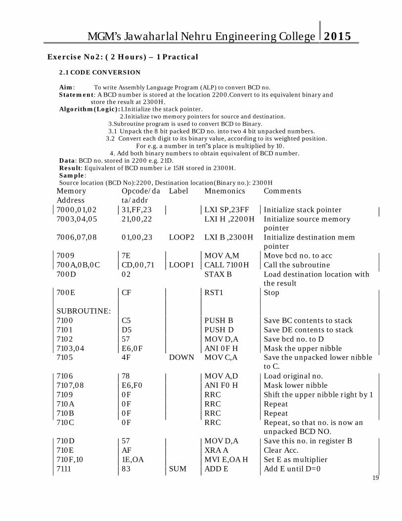
Exercise No2: ( 2 Hours) – 1 Practical
2.1 CODE CONVERSION
Aim: To write Assembly Language Program (ALP) to convert BCD no.Statement: A BCD number is stored at the location 2200.Convert to its equivalent binary and
store the result at 2300H.Algorithm(Logic):1.Initialize the stack pointer.
2.Initialize two memory pointers for source and destination. 3.Subroutine program is used to convert BCD to Binary.3.1 Unpack the 8 bit packed BCD no. into two 4 bit unpacked numbers.
3.2 Convert each digit to its binary value, according to its weighted position.For e.g. a number in ten‟s place is multiplied by 10.
4. Add both binary numbers to obtain equivalent of BCD number. Data: BCD no. stored in 2200 e.g. 21D.Result: Equivalent of BCD number i.e 15H stored in 2300H.Sample:Source location (BCD No):2200, Destination location(Binary no.): 2300H
Memory Opcode/da Label Mnemonics CommentsAddress ta/addr7000,01,02 31,FF,23 LXI SP,23FF Initialize stack pointer7003,04,05 21,00,22 LXI H ,2200H Initialize source memory
pointer7006,07,08 01,00,23 LOOP2 LXI B ,2300H Initialize destination mem
pointer7009 7E MOV A,M Move bcd no. to acc700A,0B,0C CD,00,71 LOOP1 CALL 7100H Call the subroutine700D 02 STAX B Load destination location with
the result700E CF RST1 Stop
SUBROUTINE:7100 C5 PUSH B Save BC contents to stack7101 D5 PUSH D Save DE contents to stack7102 57 MOV D,A Save bcd no. to D7103,04 E6,0F ANI 0F H Mask the upper nibble7105 4F DOWN MOV C,A Save the unpacked lower nibble
to C.7106 78 MOV A,D Load original no.7107,08 E6,F0 ANI F0 H Mask lower nibble7109 0F RRC Shift the upper nibble right by 1710A 0F RRC Repeat710B 0F RRC Repeat710C 0F RRC Repeat, so that no. is now an
unpacked BCD NO.710D 57 MOV D,A Save this no. in register B710E AF XRA A Clear Acc.710F,10 1E,OA MVI E,OA H Set E as multiplier7111 83 SUM ADD E Add E until D=0
19
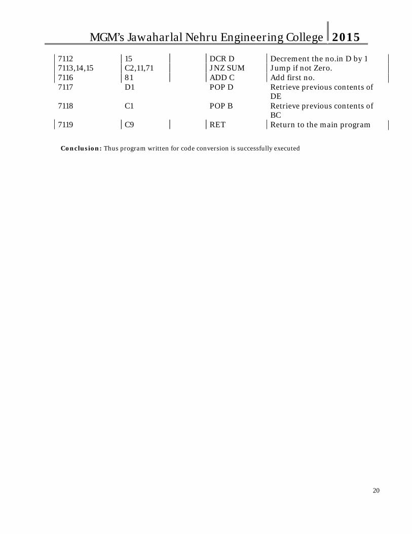
MGM’s Jawaharlal Nehru Engineering College 2015
7112 15 DCR D Decrement the no.in D by 17113,14,15 C2,11,71 JNZ SUM Jump if not Zero.7116 81 ADD C Add first no.7117 D1 POP D Retrieve previous contents of
DE7118 C1 POP B Retrieve previous contents of
BC7119 C9 RET Return to the main program
Conclusion: Thus program written for code conversion is successfully executed
20

MGM’s Jawaharlal Nehru Engineering College 2015
Exercise No3: ( 2 Hours) – 1 Practical
ADC INTERFACING WITH 8255Aim: To write a program to interface the ADC with 8255.Statement: Interface the ADC to 8255.Take analog data from the first channel, convert it in the
digital form .Use port A of 8255 and d isp lay the digi tal data .C ircuit Diagram :
Logic: Initialize 8255 with port A as i/p port, port B as output port and port Clower as input port.
Out this control word to control word register. Select the channel for taking analog data.Make the SOC(Start of conversion ) and ALE (Address Latch Enable) High. Make SOC low.
CHECK: Check EOC connected to port C of 8255 for high. If no, Jump to CHECK.If yes, clear the contents of accumulator.Read the digital data available on Port A from the ADC. Display it in the data field.
Theory: Explain ADC0808 pin diagram, block diagram and operation. Explain interfacing of ADC with 8085 with neat diagram.
ALP: Initialization and program for 8255Conclusion: The program written for ADC I/F is verified and proved correct.
21
MGM’s Jawaharlal Nehru Engineering College 2015
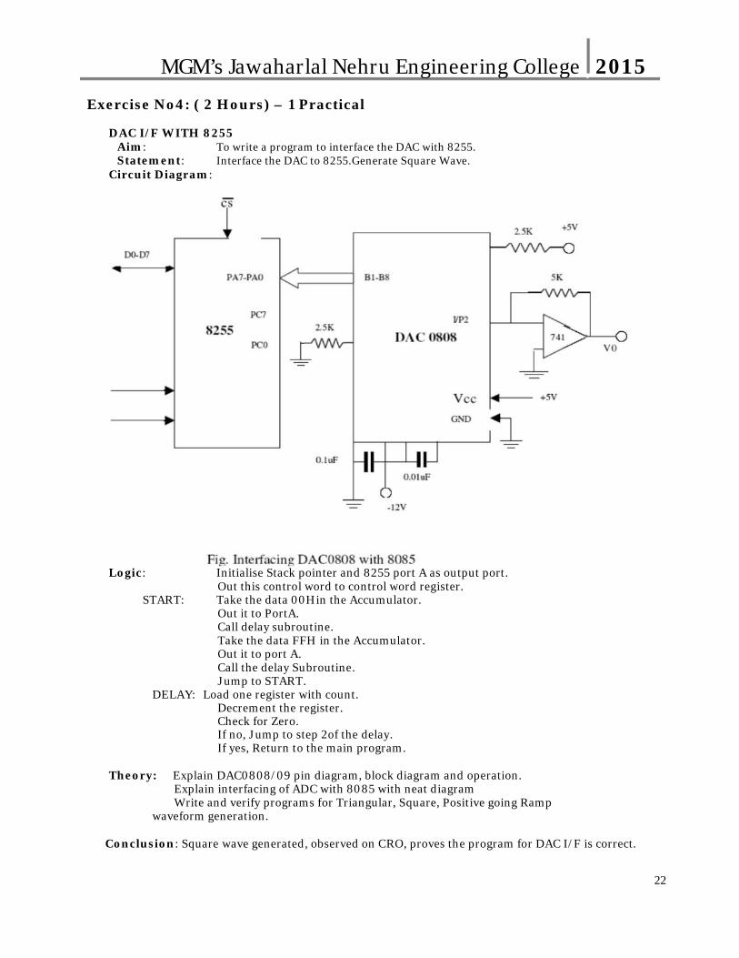
Exercise No4: ( 2 Hours) – 1 Practical
DAC I/F WITH 8255Aim: To write a program to interface the DAC with 8255.Statement: Interface the DAC to 8255.Generate Square Wave.
Circuit Diagram:
Logic: Initialise Stack pointer and 8255 port A as output port.Out this control word to control word register.
START: Take the data 00Hin the Accumulator.Out it to PortA.Call delay subroutine.Take the data FFH in the Accumulator.Out it to port A.Call the delay Subroutine.Jump to START.
DELAY: Load one register with count.Decrement the register.Check for Zero.If no, Jump to step 2of the delay.If yes, Return to the main program.
Theory: Explain DAC0808/09 pin diagram, block diagram and operation. Explain interfacing of ADC with 8085 with neat diagramWrite and verify programs for Triangular, Square, Positive going Ramp
waveform generation.
Conclusion: Square wave generated, observed on CRO, proves the program for DAC I/F is correct.
22
MGM’s Jawaharlal Nehru Engineering College 2015
Exercise No5: ( 2 Hours) – 1 Practical
RELAY INTERFACING USING 8255
Aim: Write an ALP to interface a relay with 8085 using 8255.Statement : Control the ON-OFF action of relay using any one port of 8255.Provide
appropriate delay routine.Logic: 1.Initialise stack pointer.
2 Control Word is given to control register to set ports in different modes. Port A of 8255 is used in output mode3 To make relay on data FF should be outputted on Port A. 4 Delay is provided.5 To Off the relay 00 should be outputted.6 Delay is provided.7 Repeat steps 3 to 6 for continuous operation.
Subroutine:1S.Initialise one register pair with count(Max=FFFF H). 2S.Decrement the register pair.3S.Check if the count has become zero. 4S.If no, jump to step 2S. 5S.Otherwise return to main program.
Port addresses Port A Port B Port C Control Register8255 Upper 00H 01H 02H 03H8255 Lower 08H 09H 0AH 0BH
Control Word:BSR/IO modeA PA PCu ModeB PB PCl1 0 0 0 ** * * =80H
Write a program according to the logic of the program.Theory: Explain working of a relay and the interfacing circuit.
Explain in detail the interfacing of relay with 8085Result: Relay turns ON-OFF.
23
MGM’s Jawaharlal Nehru Engineering College 2015
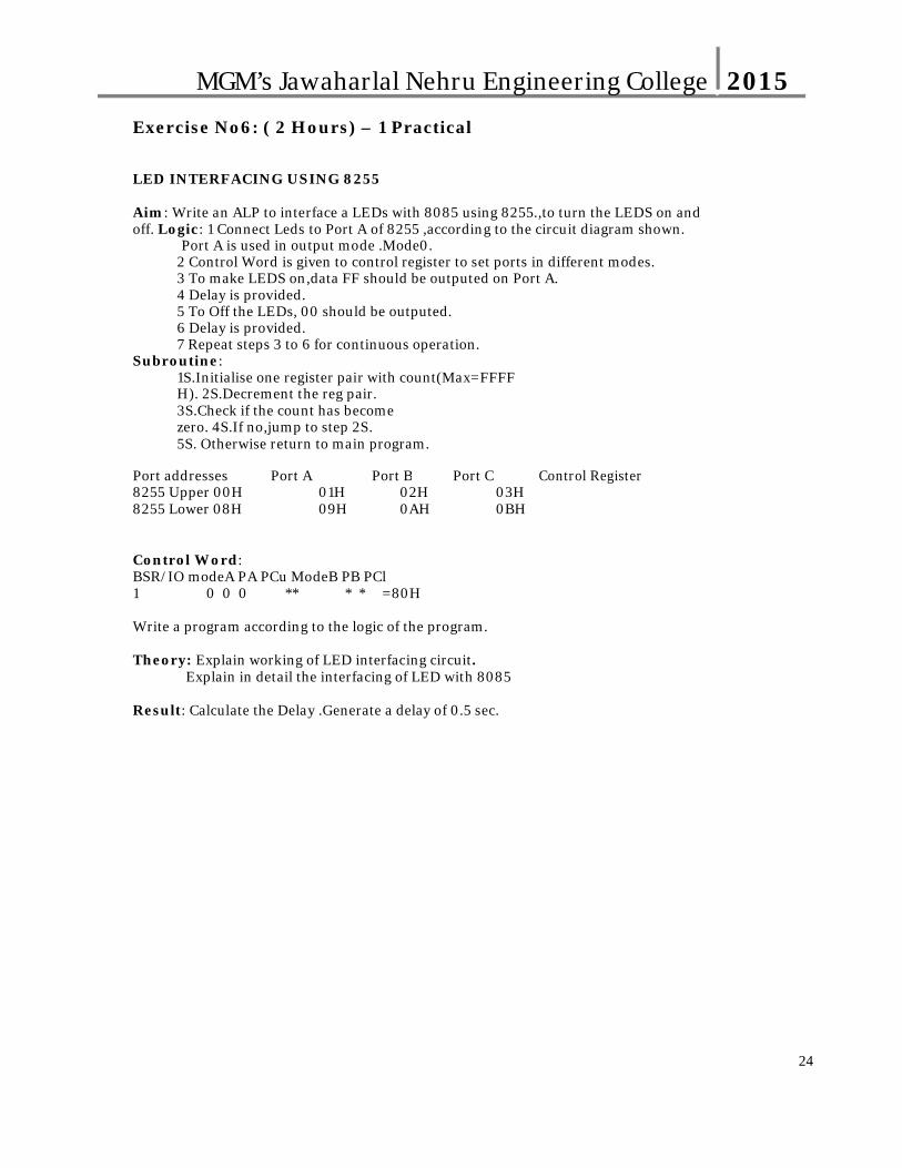
Exercise No6: ( 2 Hours) – 1 Practical
LED INTERFACING USING 8255
Aim: Write an ALP to interface a LEDs with 8085 using 8255.,to turn the LEDS on and off. Logic: 1 Connect Leds to Port A of 8255 ,according to the circuit diagram shown.
Port A is used in output mode .Mode0.2 Control Word is given to control register to set ports in different modes. 3 To make LEDS on,data FF should be outputed on Port A.4 Delay is provided.5 To Off the LEDs, 00 should be outputed.6 Delay is provided.7 Repeat steps 3 to 6 for continuous operation.
Subroutine:1S.Initialise one register pair with count(Max=FFFF H). 2S.Decrement the reg pair.3S.Check if the count has become zero. 4S.If no,jump to step 2S.5S. Otherwise return to main program.
Port addresses Port A Port B Port C Control Register8255 Upper 00H 01H 02H 03H8255 Lower 08H 09H 0AH 0BH
Control Word:BSR/IO modeA PA PCu ModeB PB PCl1 0 0 0 ** * * =80H
Write a program according to the logic of the program.
Theory: Explain working of LED interfacing circuit.Explain in detail the interfacing of LED with 8085
Result: Calculate the Delay .Generate a delay of 0.5 sec.
24
MGM’s Jawaharlal Nehru Engineering College 2015
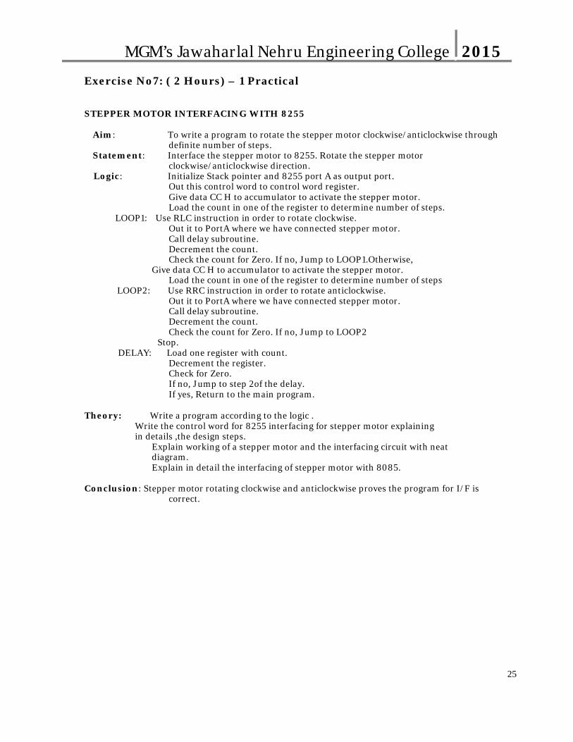
Exercise No7: ( 2 Hours) – 1 Practical
STEPPER MOTOR INTERFACING WITH 8255
Aim: To write a program to rotate the stepper motor clockwise/anticlockwise throughdefinite number of steps.
Statement: Interface the stepper motor to 8255. Rotate the stepper motorclockwise/anticlockwise direction.
Logic: Initialize Stack pointer and 8255 port A as output port.Out this control word to control word register.Give data CC H to accumulator to activate the stepper motor.Load the count in one of the register to determine number of steps.
LOOP1: Use RLC instruction in order to rotate clockwise.Out it to PortA where we have connected stepper motor.Call delay subroutine.Decrement the count.Check the count for Zero. If no, Jump to LOOP1.Otherwise,
Give data CC H to accumulator to activate the stepper motor.Load the count in one of the register to determine number of steps
LOOP2: Use RRC instruction in order to rotate anticlockwise.Out it to PortA where we have connected stepper motor.Call delay subroutine.Decrement the count.Check the count for Zero. If no, Jump to LOOP2
Stop.DELAY: Load one register with count.
Decrement the register.Check for Zero.If no, Jump to step 2of the delay.If yes, Return to the main program.
Theory: Write a program according to the logic .Write the control word for 8255 interfacing for stepper motor explaining in details ,the design steps.
Explain working of a stepper motor and the interfacing circuit with neat diagram.Explain in detail the interfacing of stepper motor with 8085.
Conclusion: Stepper motor rotating clockwise and anticlockwise proves the program for I/F iscorrect.
25
MGM’s Jawaharlal Nehru Engineering College 2015
Exercise No8: ( 2 Hours) – 1 Practical
STUDY OF 8253
Aim: Study 8253, “The programmable interval timer”Description: Explain:
1. Features of 8253.2. Pin diagram ,Block diagram and functional description of 8253.3. Modes of 8253(e.g 8253 is a Programmable interval timer IC working in
6 different modes-Modes0 to5.Mode 0 is Interrupt on terminal count mode.Mode 1 is Programmable one shot mode.Mode 2 is Rate/Pulse generator mode.Mode 3 is square wave generator mode.Mode 4 is software triggered strobe.Mode 5 is Hardware triggered strobe.
Explain each mode in detail considering different cases with neat diagrams4. Write the control word for 8253.
5. 8253 interfacing with 8085.
Exercise No 9: (2 Hours) – 1 Practical
11 STUDY OF 8259
Aim: Study of the priority interrupt controller 8259Description: Explain
1. Features of 8259.2. Pin diagram, Block diagram and functional description of 8259.3. Priority modes of 8259.4.8259 interfacing5. Cascading of 8259
26
MGM’s Jawaharlal Nehru Engineering College 2015
3.Quizonthesubject:
Quiz should be conducted on tips in the laboratory, recent trends and subject knowledge of the subject. The quiz questions should be formulated such that questions are normally are from the scope outside of the books. However twisted questions and self formulated questions by the faculty can be asked but correctness of it is necessarily to be thoroughly checked before the conduction of the quiz.
Sample Questions:1. Define Microprocessor.2. Define stack, stack pointer.3. Define Memory.4. What is RAM? Is RAM a volatile memory?5. What is ROM? Is ROM used to store the binary codes for the instructions or lookup table?Why?6. What is the function of „Timing and control unit‟ in microprocessor?7. Which are the different types of buses used in microprocessor?8. Explain fetching, decoding and execution operations of microprocessor.9. Explain the difference between PROM,EPROM AND EEPROM.10. Explain Different Blocks Of Microprocessor.11. How many data lines, address lines are present in 8085.12. How many address lines are required to access 2MB of memory.13. List the internal registers in 8085.Describe the primary function of each register.14. Give the clock frequency of 8085 operating with each of following
frequency crystals:6.25MHZ,6.144MHz,5MHz,4MHz15. Give the format of Flag Register in 8085.Explain each flag.16. Why AD0-AD7 lines are multiplexed?17. What is the use of ALE signal?18. What is the use of „clock out‟ and „reset out‟ signals of 8085?19. Describe function of following pins in 8085:
(1) READY (2) ALE (3) IO/M‟ (4) HOLD (5) RESET20. List the instructions related to DMA operation in 8085.21 Stress out the necessity of having two status lines S1 and S0 in 8085.22 List out different control signals used by 8085.23 On power on reset, what is the content of PC ?24. List the instructions related to serial operation in 8085.25. List the different addressing modes of 8085.26. Explain following instructions:
1) PUSH 2)POP 3)CALL 4)RET27. Explain 8255.28 Explain 8253.29. Explain 8257.30. Explain 8279.31. Explain 8259.
27

MGM’s Jawaharlal Nehru Engineering College 2015
4.ConductionofViva-VoceExaminations:
Teacher should conduct oral exams of the students with full preparation. Normally, the objective questions with guess should be avoided. To make it meaningful, the questions should be such that depth of the students in the subject is tested. Oral examinations are to be conducted in cordial environment amongst the teachers taking the examination. Teachers taking such examinations should not have ill thoughts about each other and courtesies should be offered to each other. Difference of opinion, if any, should be critically suppressed in front of the students.
5.Evaluationandmarkingsystem:
Basic honesty in the evaluation and marking system is absolutely essential and in the process impartial nature of the evaluator is required in the examination. It is a wrong approach to award the students by way of easy marking to get cheap popularity among the students, which they do not deserve. It is a primary responsibility of the teacher to see that right students who are really putting up lot of hard work with right kind of intelligence are correctly awarded.
The marking patterns should be justifiable to the students without any ambiguity and teacher should see that students are faced with just circumstances.
28