microwave active devices and circuits fabrication technologies
TRANSCRIPT

Microwave active devices and circuits fabrication
technologies

Main Semiconductors Parameters
350

Comparison between Silicon and GaAs
Pros of GaAs:• Lower transit time of electric charge• Higher max temperature (350° vs. 200°)• Higher radiation resistance• Substrate with higher resistivity (better intrinsic isolation, low
parassitics)Cons of GaAs:• Low mechanical robustness• Low thermal conductivity• Difficult to limit impurities (Not possible to fabricate good MOS
devices)

Bipolar Transistors
Power devices structure
p+
p+
p+
p+
p
p
n epitaxy
n+
n epitaxy
pn buried layer
+
Emitter
Base
Active Transistor Region
Collector
n +
n +
i B
iC
n+
iE
p
p
p
p

Unipolar Transistors

MESFET (Metal-Semiconductor gate)
• High carriers mobility High current high working frequency
• Key parameter: Channel length L• It is possible to realize only n channel devices• Intrinsic isolation (not doped substrate)

High Mobility Transistors (HEMT)
Heterojunction: junction between semiconductor with different band-gap(GaAlAs and GaAs in the figure)The n-GaAlAs layer is used for realizing the gate MS junctionAt the interface between GaAlAs and GaAs is generated a layer of electrons with a very high horizontal mobility (bi-dimensional gas).The source-drain conductivity is controlled by the source-gate voltage (as in MESFETs)

Properties of HEMTs
• High electrons mobility in the bi-dimensional gas: 7000-8000 cm2v-1s-1
vs. 5000 cm2v-1s-1 in doped n GaAs• The mobility even increases by refrigerating the device: at 77 °K we get
70000 cm2v-1s-1. Also noise performances improve• The drain-source channel is better confined with respect to MESFETs;
as a consequence the small signal transconductance increases even for small values of drain current. Also the noise figure and the output conductance improve
• Recently the pHEMT (pseudomorphic HEMT) has been introduced. It is characterized by an additional layer of InGaAs between GaAs and GaAlAs. The maximum operating frequency is so further increased; also ID current, for a given geometry and applied voltages, increases by a factor 2 with respect to a traditional HEMT
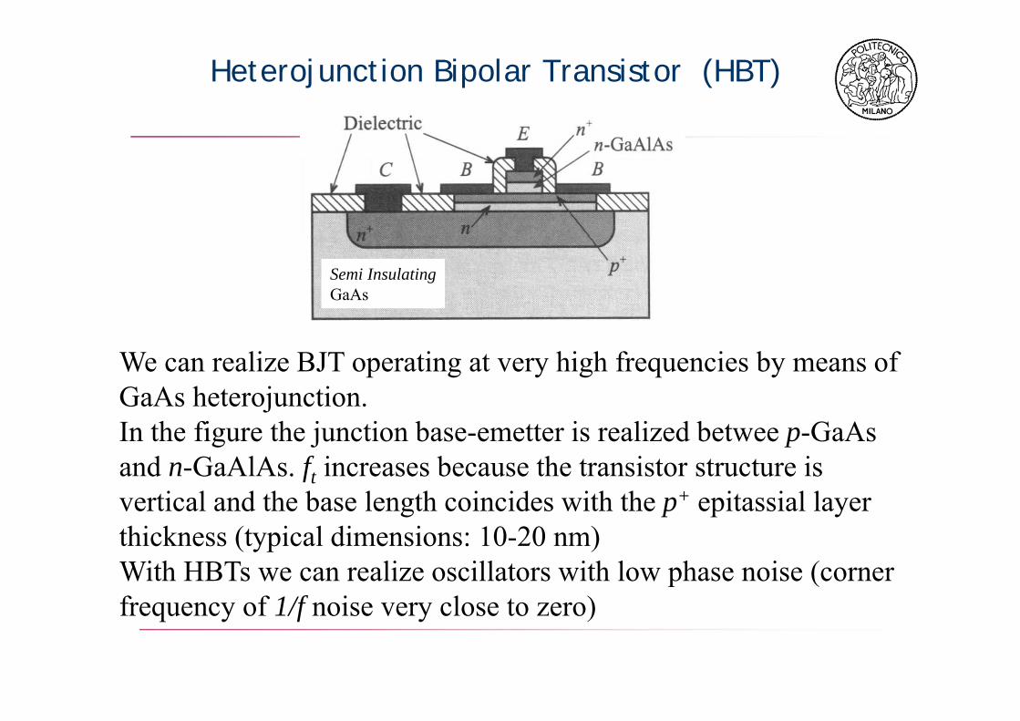
Heterojunction Bipolar Transistor (HBT)
Semi InsulatingGaAs
We can realize BJT operating at very high frequencies by means of GaAs heterojunction.In the figure the junction base-emetter is realized betwee p-GaAs and n-GaAlAs. ft increases because the transistor structure is vertical and the base length coincides with the p+ epitassial layer thickness (typical dimensions: 10-20 nm)With HBTs we can realize oscillators with low phase noise (corner frequency of 1/f noise very close to zero)

Fabrication technologies of planar microwave circuits
Traditional printed board: Single dielectric layer (metallized at one side) Active and passive discrete components (surface
mount, via hole, etc.) Interconnections, lines and distributed components
realized through “printing” Integrated Circuits:
Hybrid Technologies (thick film, thin film, LTCC…) Monolithic Technologies (MMIC on GaAs, SiGe…)
Packaging Modules inside metallic carrier Case for integrated circuits (interconnections,…)

Photolithography: geometric patterns drawn on dielectric substrates
A sensitive emulsion to ultraviolet light (photoresist) is deposited over a rigid substrate covered with SiO2. The image of the pattern is generated on a photographic film (photomask)
La photomask is placed over the photoresist and is exposed to ultraviolet light (photoresist is impressed)
Negative image: with a chemical etching the photoresist is removed where it is not impressed (in the end oxide is removed in correspondence of the pattern)
Positive image: The impressed photoresist is removed (in the end oxide remains in correspondence of the pattern)
With a suitable chemical solvent oxide is removed where it is not protected by the remaining photoresist

From the electrical circuit to the physical realization
RESID=R5R= 300 Ohm
RESID=R3R= 18 Ohm
RESID=R4R= 300 Ohm
MLINID =TL 1W =75 milL=2 00 milMSUB= sub1
MLINID =TL 7W =25 milL=5 milMSU B= sub1
MLINID=TL8W =3 0 milL= 95 mi lMSUB=sub1
MLINID=TL 12W =10 milL=5 0 milMSU B= sub1
MLINID= TL13W= 10 mi lL=50 milMSUB=sub1
MLINID=T L10W =75 milL= 50 mi lMSUB= sub1
MLINID=T L9W =19 0 milL= 120 mi lMSUB=sub1
MLINID =TL 2W =10 milL=6 8 mil
1 2
3
MTEEID =Te e2W 1=10 milW 2=10 milW 3=10 milMSUB= su b1
MLINID=T L11W =1 0 milL =268 mil
MSUBEr=3.38H= 32 mi lT =0.7 mi lRho =1T and=0 .00 22ErNom=3.38Name= sub1
MRSTUB2ID=stub2Ri= 10 mi lRo= 185 mi lTh eta =60 DegMSU B= sub1
MRSTUB2ID=stub1Ri= 10 mi lRo= 185 mi lT heta =60 DegMSUB= sub1
CH IPCAPID=C1C= 3.3 pFQ=538 .4FQ= 0.5 GHzFR=5.1362 G HzALPH= 1
R ESID= R6R =51 Ohm
CHIPCAPID=C5C= 1000 pFQ =262.4F Q=0 .00 1 G HzF R=0.247 GH zALPH=1
RESID=R2R= 51 Ohm
CHIPCAPID=C3C=1 000 pFQ= 262.4FQ =0.001 G HzFR =0.247 GHzALPH=1
CH IPCAPID=C 2C= 3.3 p FQ =538 .4F Q= 0.5 G HzF R=5.136 2 G HzALPH= 1
MLINID=TL 14W =75 milL=2 36 mi lMSU B= sub1
MLINID=T L15W =5 0 milL= 10 mi lMSUB=sub1
ML INID= TL1 6W= 50 milL=10 milMSUB= su b1
MSTEPX$ID=MS4Of fset= 0 mi l
MSTEPX$ID=MS5O ffset=0 mil
MSTEPX$ID =MS6Offse t= 0 mil
12
3
MTEEX$ID=MT1
12
3
MT EEX$ID= MT 2
1
2
3
SUBCKTID=S1NET= "fsx0 17wf1"
1 2
3
SUBC KTID= S2NET=" Inpu t Matchi ng Netwo rk"
PORTP=1Z=50 Ohm PORT
P=2Z =50 Ohm
7 GHz Microwave FET Amplifier
Circuit
Layout (single layer)
RealizationSubstrate: FR4Conductor: CopperMask: PositiveRemoval of excess cupper: through chemical solvent

Technological Limits of traditional printed board
Minimum geometric dimensions limited by accuracy (typically 30-100 m)
Components density limited by the case size of discrete components
Electromagnetic interactions between the circuit and the case (spurious resonances)
Problems increase as the frequency becomes higher and higher

Hybrid integrated circuits
Hybrid integrations allows:
To realize passive components with the same process used for the metallic patterns
To employ active components without the case ( size reduction)
To increase the accuracy of the geometric pattern (Minimum dimensions of lines/gap 10-50 m)
To increase components density through the use of multilayer structures

“Thin Film” Integrated Circuits
The “Thin Film” technology allows to integrate on the substrate:- Conductive lines and microstrip- Resistors- Inductors- Capacitors- Cross-over
“Thin Film” refers to the material layers deposited on a substrate,generally insulant, with very small thickness (order of magnitude0,1 µm). The property of the layers are strongly affected by thethickness as well as by the process characteristics of the layerdeposition.

Substrate Characteristics
Uniformity and anisotropy of dielectric constant
Thickness uniformity Uniformity of surface roughness Mechanical robustness Thermal expansion coefficient (low) Thermal conductivity (good)

Common substrates materials
Common Substrates Materials and Their Applications
Material Typical Users CommentsAlimina (Al2O3) 99.6% Low to medium power DC/RF or
Microwave circuits using Si or GaAsIcs
Cost-effective material withwide range of applications
Beryllia (BeO) High-power DC/RF/Microwavecircuits using Silicol or GaAs Ics. Highpower terminations
Extremely high thermalconductivity
Aluminium-Nitride (AlN) High-power DC/RFMicrowave circuitsusing silicon and GaAs ICs
Optimal CTE match withsilicon devices
Quartz (SiO2) Microwave/millimeter-wave circuitsrequiring extremely low loss or lossCTE
Low Loss Tangent and GTESmooth surface finish
Titanates RF/Microwave amplifier or oscillatorsrequiring High-Q resonators andtransformers
Dielectric constantsavailable from 12-100
Ferrite RF/Microwave circulator/isolators Magnetically activatedmaterial
Sapphire Millimeter-wave/optical circuits withspecial electrical or mechanicalrequirements
Low Loss Tangent, Opticalsurface finish

Materials employed in thin film technology
Conductors:• Gold (3-9 m, galvanic)• Palladium (2500 Å, sputtering)• Titanium (500 Å, sputtering)
They increase the conductivity and guarantee adherence with the underlying layer
Resistors:• Tantalum• NiCr
Minimum dimensions of lines/gaps: 10-50 mAccuracy: 2-10 m

Film realization
Sputtering:A plasma gas is created into areactor starting from the materialto be deposited (sputtered). Thecharged particles are acceleratedand pushed against the substrateupon which are deposited creatingthe film (thickness 500-3000 A)
Electrochemical:Growth through galvanic process.

Fabrication of a thin film circuit (1)
Substrate Tantalum Layer (resistors)
Titanium Layer(conductors)
Palladium Layer(adhesive)
Photoresist Conductor Pattern+ resistors
Gold deposition(galvanic)
Photoresist removal

Palladium removal Titanium removal +Gold galvanic growth
Photoresist coating Resistor Pattern
Gold + Palladium removal
Titanium removal Photoresist removal
Fabrication of a thin film circuit(2)

Machining
Via hole: Realization of a inner metalized hole (gold).Via holes belong to conductive layers; the hole in thesubstrate is realized by a laser before the conductivelayers suttering
Substrate drilling: it is requested also for fixing thecircuit in the case (through screws). It is realized with alaser o ultrasonic drill after the circuit realization

Other components: air bridges

Examples

“Thick Film” circuits
This technology is more convenient (less expensive) with respectthe thin film when a lower accuracy is requested (and theproduction volume is smaller)
General features:
• Minimum dimensions: 50-100 m• Accuracy: 10-50 m• Pattern transferred on a wire screen mesh • Substrates: similar to thin film technology • Materials:
– Conductors: Gold, copper, silver– Resistors: special mixture of resins
• Multi layers circuits possible

Realization of a thick film circuit

Possibilities of thick film

Basic Components

Examples of thick film circuits
Filtro a 38 GHz “Edge-coupled”Amplificatore lineare 13-15 GHz

Examples of complete systems

LTCC Technology (notes)
“LTCC” is an acronym for:Low Temperature Co-fired Ceramic
With this integration technology is possible realize multi-layerextremely compact structures with passive components. Activecomponents can be added on the top and bottom layers

Realization of LTCC circuits

Packaging of microwave circuits
Traditional solution:The circuit is inserted into a metallic container (carrier)
Innovative solution“Chip & Wire” Technology : carrier of compact dimensions; wired external connections. Suitable for chip components (without case)