microwave system design considerations. misunderstanding of complete system system will surely fail...
Post on 21-Dec-2015
214 views
TRANSCRIPT

MICROWAVE SYSTEM DESIGN
CONSIDERATIONS
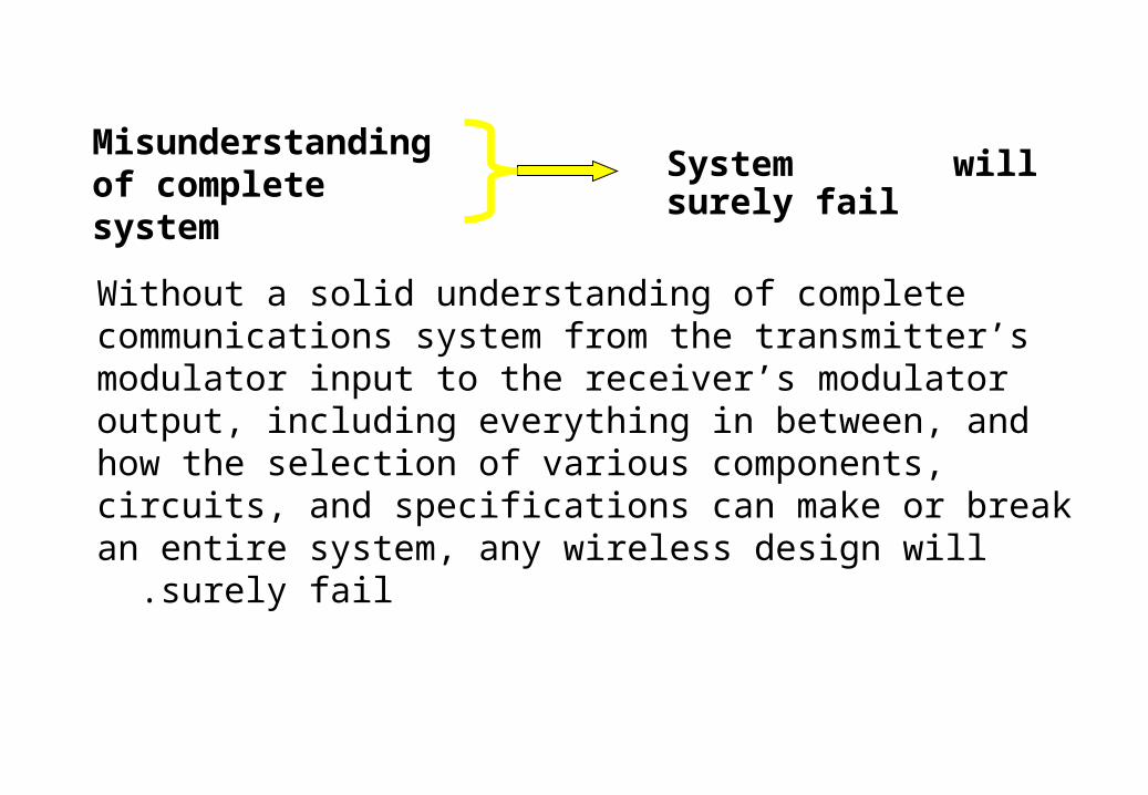
Misunderstanding of complete system
System will surely fail
Without a solid understanding of complete communications system from the transmitter’s modulator input to the receiver’s modulator output, including everything in between, and how the selection of various components, circuits, and specifications can make or break
an entire system, any wireless design will surely fail .
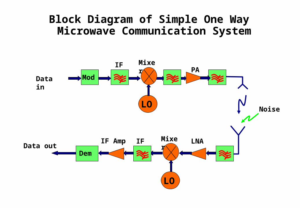
PAIF Mixer
ModData in
LONoise
LNAMixerIF Amp IF Data out
LO
Dem
Block Diagram of Simple One Way Microwave Communication System

Baseband: Data, Voice, Video,….etc BW?
Modulation: Digital or Analog
Transmitter Components: IF Filters Mixer (up conversion)Filter PA RF FiltersAntenna
Link Calculation:Satellite Terrestrial Radar Wireless Mobile,
…..etc Receiver Components: Antenna RF Filters LNA Mixer (down conversion) IF Filters IFAmplifier
Demodulator
Other Components:Control System & Power Supply Monitoring: Test and measuring components & Measuring tools
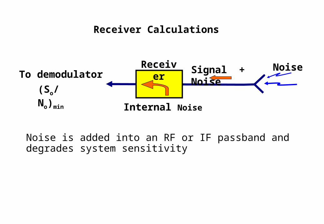
Receiver Calculations
Noise
(So/No)min
ReceiverTo demodulator Signal + Noise
Internal Noise
Noise is added into an RF or IF passband and degrades system sensitivity
The receiving system does not register the difference between signal power and noise power. The external source, an antenna, will deliver both signal power and noise power to receiver. The system will add noise of its own to the input signal, then amplify the total package by the power gain
Noise behaves just like any other signal a system processes
Filters: will filter noise
Attenuators: will attenuate noise
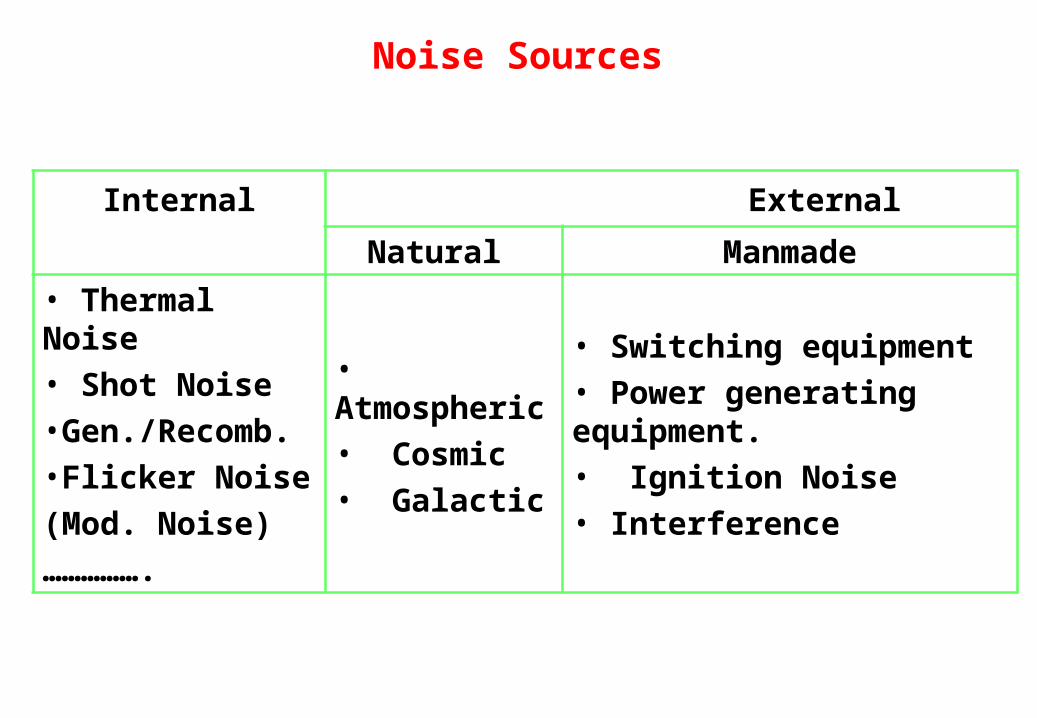
ExternalInternal
ManmadeNatural
• Switching equipment
• Power generating equipment.
• Ignition Noise
• Interference
• Atmospheric
• Cosmic
• Galactic
• Thermal Noise
• Shot Noise
•Gen./Recomb.
•Flicker Noise
(Mod. Noise)
…………….
Noise Sources
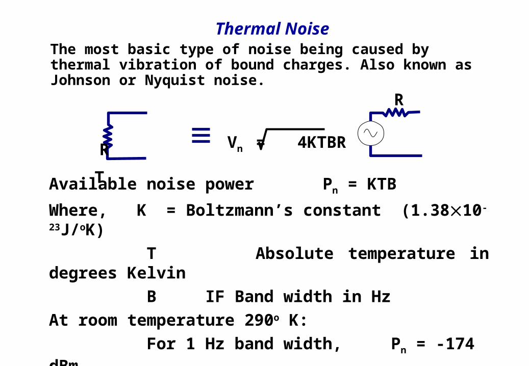
Thermal NoiseThe most basic type of noise being caused by thermal vibration of bound charges. Also known as Johnson or Nyquist noise.
R
T Vn = 4KTBR
R
Available noise power Pn = KTB
Where, K = Boltzmann’s constant (1.3810-23J/oK)
T Absolute temperature in degrees Kelvin
B IF Band width in Hz
At room temperature 290o K:
For 1 Hz band width, Pn = -174 dBm
For 1 MHz Bandwidth Pn = -114 dBm
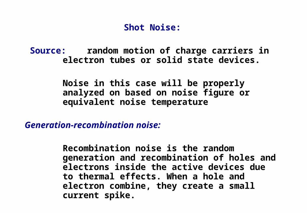
Shot Noise:
Source: random motion of charge carriers in electron tubes or solid state devices.
Noise in this case will be properly analyzed on based on noise figure or equivalent noise temperature
Generation-recombination noise:
Recombination noise is the random generation and recombination of holes and electrons inside the active devices due to thermal effects. When a hole and electron combine, they create a small current spike.
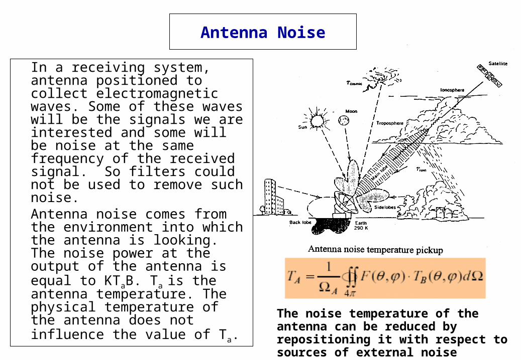
Antenna Noise
In a receiving system, antenna positioned to collect electromagnetic waves. Some of these waves will be the signals we are interested and some will be noise at the same frequency of the received signal. So filters could not be used to remove such noise.Antenna noise comes from the environment into which the antenna is looking. The noise power at the output of the antenna is equal to KTaB. Ta is the antenna temperature. The physical temperature of the antenna does not influence the value of Ta.
The noise temperature of the antenna can be reduced by repositioning it with respect to sources of external noise
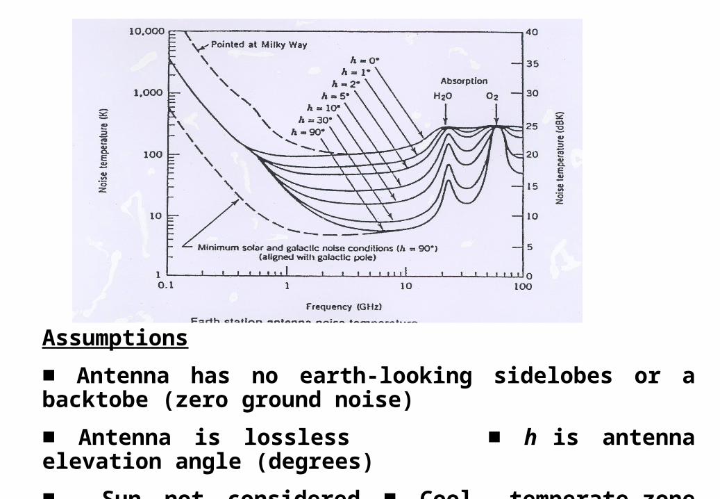
Assumptions
■ Antenna has no earth-looking sidelobes or a backtobe (zero ground noise)
■ Antenna is lossless ■ h is antenna elevation angle (degrees)
■ Sun not considered ■ Cool. temperate-zone troposphere
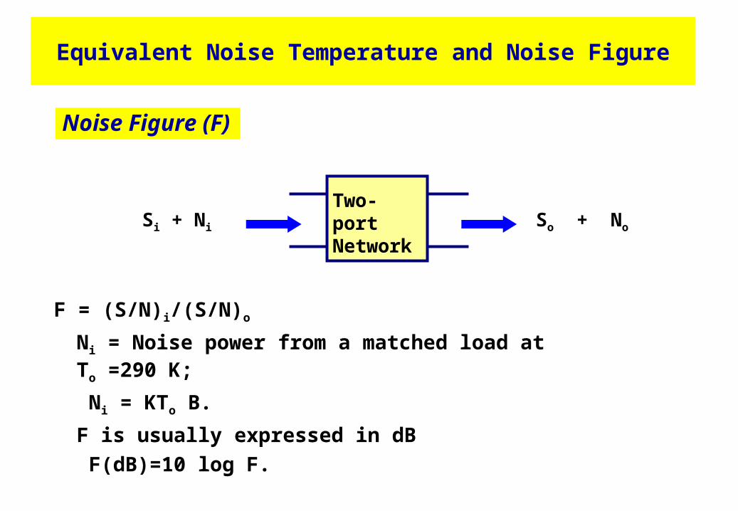
Equivalent Noise Temperature and Noise Figure
F = (S/N)i/(S/N)o
Ni = Noise power from a matched load at To =290 K;
Ni = KTo B.
F is usually expressed in dB
F(dB)=10 log F.
Noise Figure (F)
Two-portNetworkSi + Ni So + No

Te = No/KB, B is generally the bandwidth of the component or system
Te = To( F – 1)
To is the actual temperature at the input port, usually 290 K
R No
white noise
source R R
Te No
Equivalent Noise Temperature (Te)
If an arbitrary noise source is white, so that its power spectral density is not a function of frequency, it can be modeled as equivalent thermal noise source and characterized by Te.
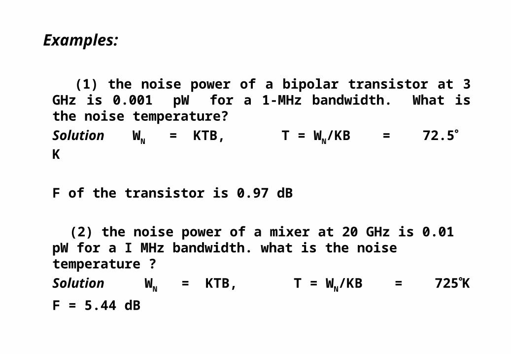
Examples:
(1) the noise power of a bipolar transistor at 3 GHz is 0.001 pW for a 1-MHz bandwidth. What is the noise temperature?
Solution WN = KTB, T = WN/KB = 72.5 K
F of the transistor is 0.97 dB
(2) the noise power of a mixer at 20 GHz is 0.01 pW for a I MHz bandwidth. what is the noise temperature ?
Solution WN = KTB, T = WN/KB = 725K
F = 5.44 dB
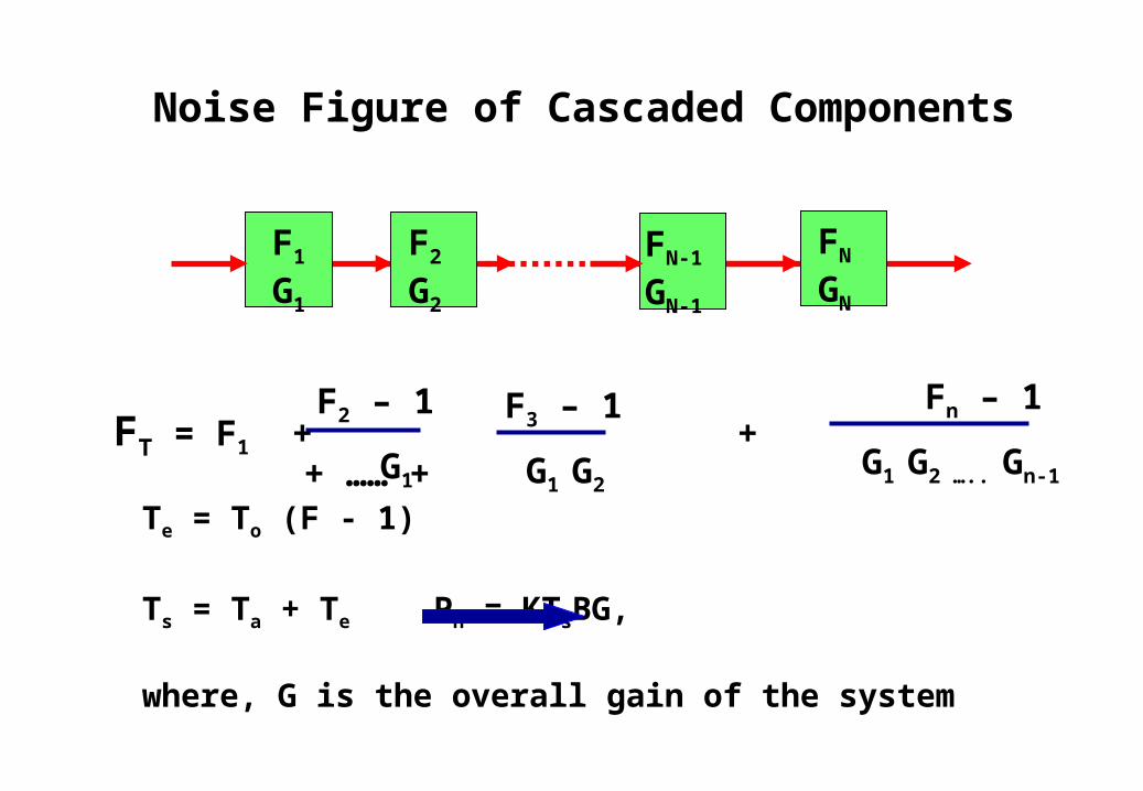
Noise Figure of Cascaded Components
Te = To (F - 1)
Ts = Ta + Te Pn = KTsBG,
where, G is the overall gain of the system
F2 – 1
G1
F3 – 1
G1 G2
Fn – 1
G1 G2 ….. Gn-1
FT = F1 + + + …… +
F1
G1
F2
G2
FN-1
GN-1
FN
GN
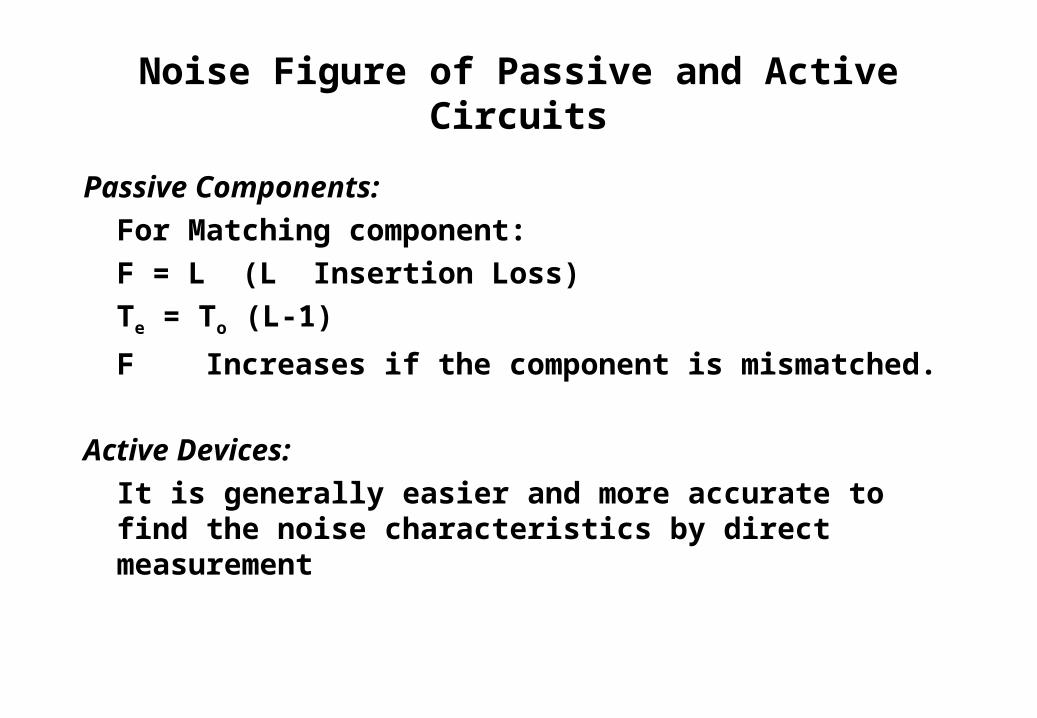
Noise Figure of Passive and Active Circuits
Passive Components:
For Matching component:
F = L (L Insertion Loss)
Te = To (L-1)
F Increases if the component is mismatched.
Active Devices:
It is generally easier and more accurate to find the noise characteristics by direct measurement
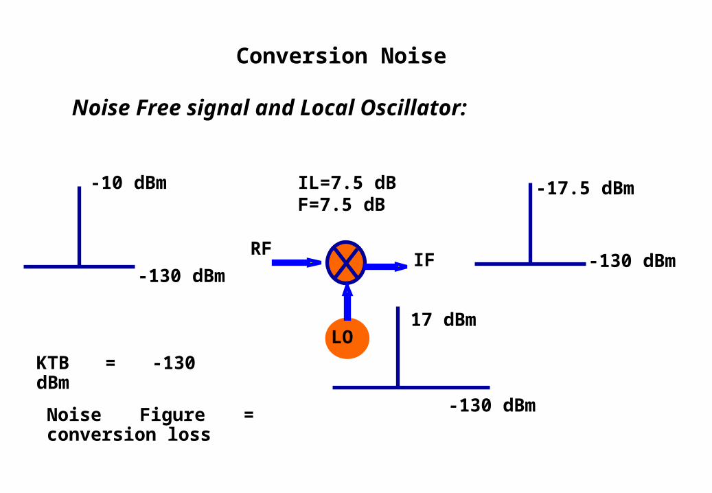
Conversion Noise
Noise Free signal and Local Oscillator:
-10 dBm
-130 dBm
-17.5 dBm
-130 dBm
IL=7.5 dBF=7.5 dB
LO
RFIF
KTB = -130 dBm
17 dBm
-130 dBmNoise Figure = conversion loss

Noisy received signal:
17 dBm
-130 dBm
-17.5 dBm
-97.5 dBm
IL=7.5 dBF=7.5 dB
-10 dBm
-90 dBm
-130 dBmLO
RF IF
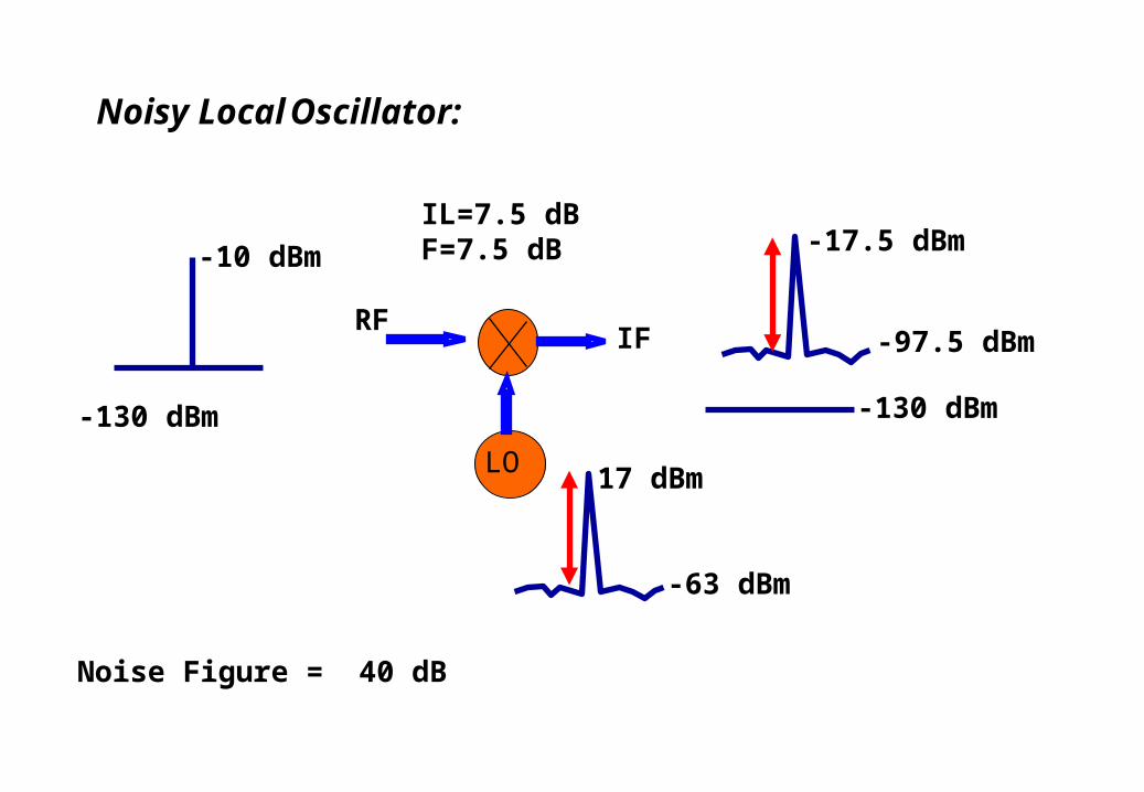
Noisy Local Oscillator:
-10 dBm
-130 dBm
IL=7.5 dBF=7.5 dB -17.5 dBm
-97.5 dBm
-130 dBm
17 dBm
-63 dBm
LO
RFIF
Noise Figure = 40 dB

Example: FT? Ts ? No ? Given IF bandwidth = 10 MH
NoiseLNAMixer
LO
BPF
G = 10 dB
Ta = 15 KF = 2 dBL = 1 dB
L = 3 dBF = 4 dB
So , No
Si , Ni
1) dB to numerical valuesLNA G = 10 dB (10) BPF: G = -1 dB (0.79) Mixer: G = -3 dB (0.5)
F = 2 dB (1.58) F = 1 dB (1.26) F = 4 dB (2.51)
2) FT = [ 1.58 + 0.26/10 + 1.51 /7.9] = 1.8 (2.55 dB)
3) Te = To(F-1) = 290 (1.8 – 1) = 232 K
4) Ts = Ta + Te = 247 K5) No = KTsBG,
G is the overall Gain = G1×G2×G3×….=10 × 0.79 × 0.5 = 3.95 (~6dB)No = -98.7 dBm
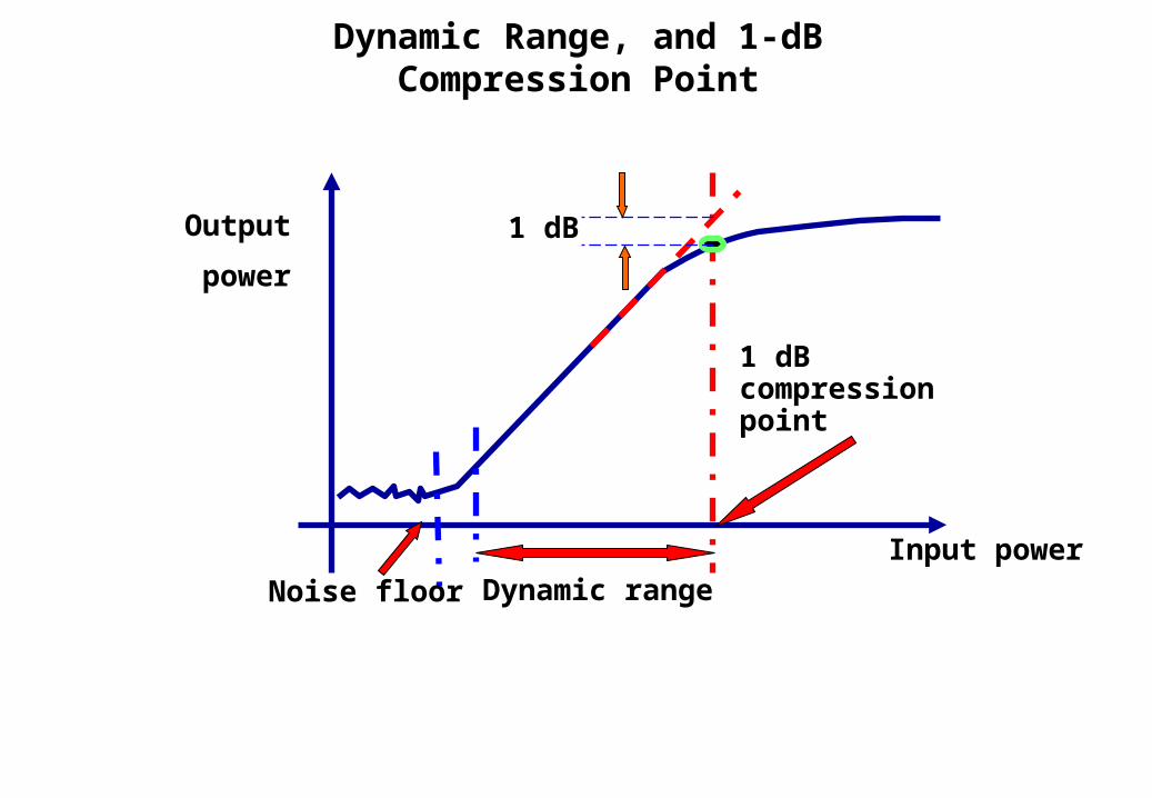
Dynamic Range, and 1-dB Compression Point
Input power
1 dB compression point
Output
power
1 dB
Dynamic rangeNoise floor

Minimum Detectable Signal (MDS)
MDS is dependent of the type of modulation used in receiving systems as well as the noise characteristics of the antenna and receiver. For a given system noise power, the MDS determines the minimum signal to noise ratio (SNR) at the demodulator of the receiver. The usable SNR depends on the application, with some typical values below
System SNR (dB)
Analog telephone 25-30
Analog television 45-55
AMPS cellular 18
QPSK (Pe = 10-5) 10

Ci/Ta Can be measured immediately following the receiver
Detector: Removes the signal from the carrier
S/N Can be determine
Noise
(Co/No)min
Receiver
TeFG
To demodulatorCi & Ta
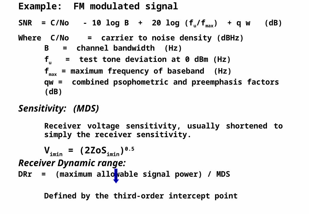
Example: FM modulated signal
SNR = C/No - 10 log B + 20 log (fu/fmax) + q w (dB)
Where C/No = carrier to noise density (dBHz)B = channel bandwidth (Hz)
fu = test tone deviation at 0 dBm (Hz)
fmax = maximum frequency of baseband (Hz)
qw = combined psophometric and preemphasis factors (dB)
Sensitivity: (MDS)
Receiver voltage sensitivity, usually shortened to simply the receiver sensitivity.
Vimin = (2ZoSimin)0.5
Receiver Dynamic range: DRr = (maximum allowable signal power) / MDS
Defined by the third-order intercept point
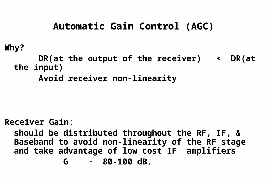
Automatic Gain Control (AGC)
Why?DR(at the output of the receiver) < DR(at the input)Avoid receiver non-linearity
Receiver Gain: should be distributed throughout the RF, IF, & Baseband to avoid
non-linearity of the RF stage and take advantage of low cost IF amplifiers
G ~ 80-100 dB.
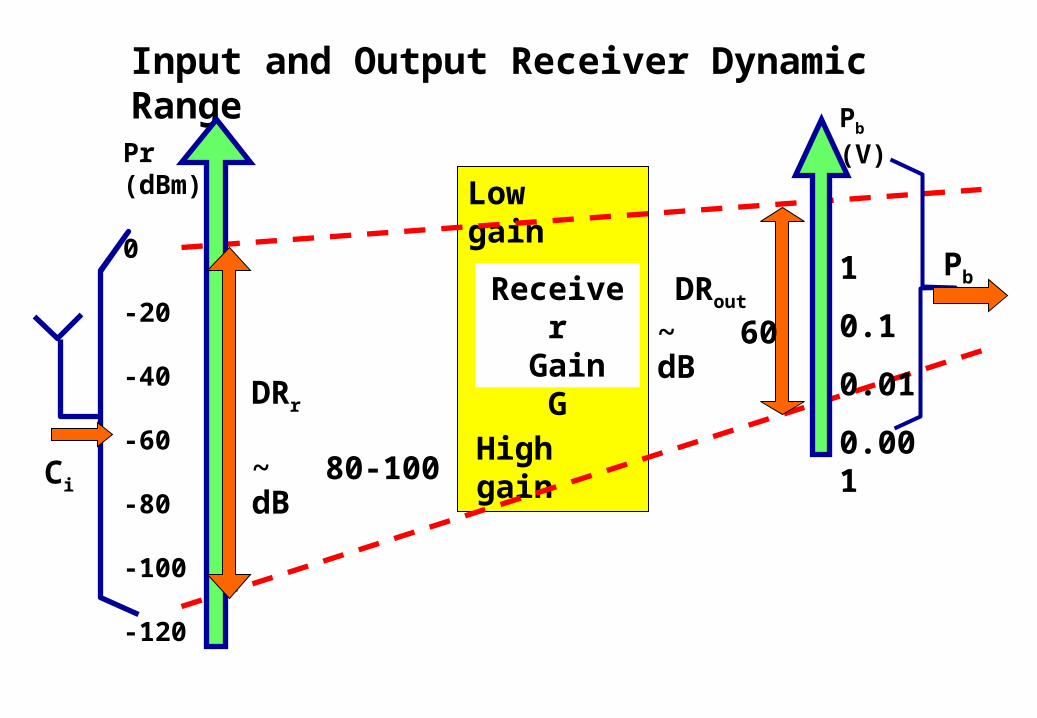
Input and Output Receiver Dynamic Range
Pr(dBm)
0
-20
-40
-60
-80
-100
-120
DRr
DRoutReceiver Gain
G
Low gain
High gainCi
Pb (V)
1
0.1
0.01
0.001
Pb
~ 80-100 dB
~ 60 dB
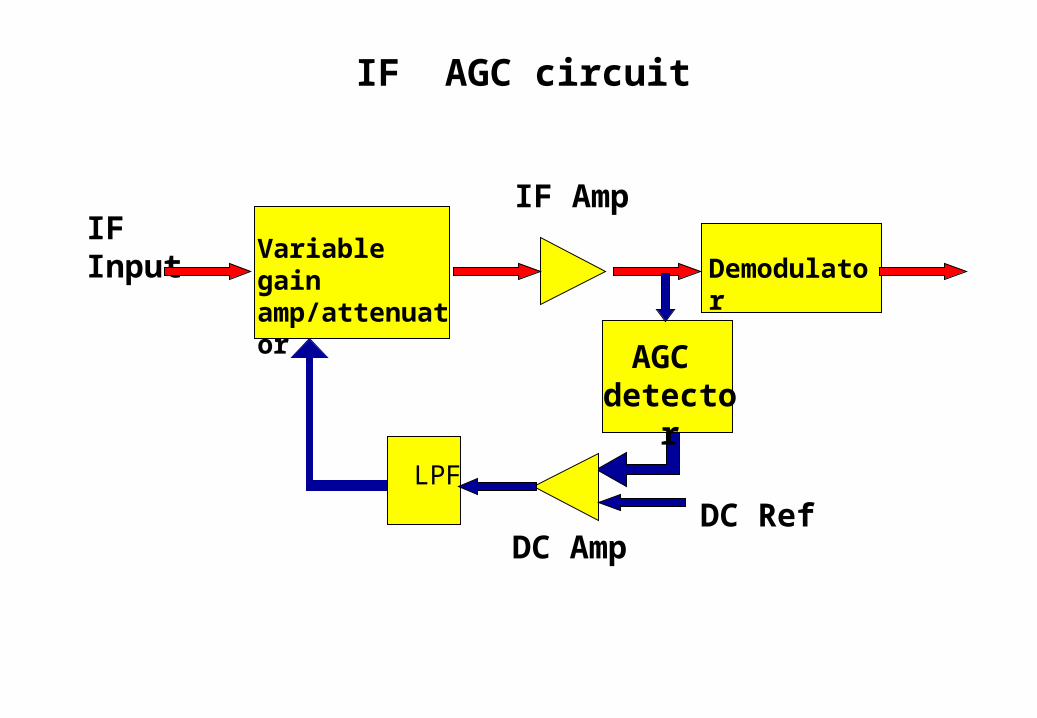
IF AGC circuit
IF Amp
Demodulator
LPF
Variable gain amp/attenuator
IF Input
DC AmpDC Ref
AGC detector
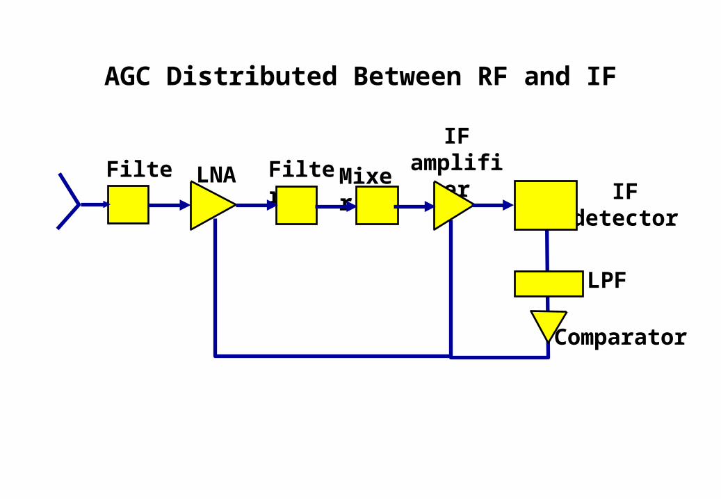
AGC Distributed Between RF and IF
IFdetector
IF amplifierFilter LNA MixerFilter
LPF
Comparator
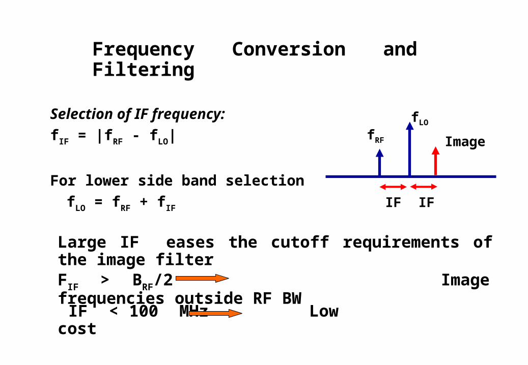
Selection of IF frequency:
fIF = |fRF - fLO|
For lower side band selection
fLO = fRF + fIF
Frequency Conversion and Filtering
Large IF eases the cutoff requirements of the image filter
FIF > BRF/2 Image frequencies outside RF BW
IF < 100 MHz Low cost
fLO
fRF Image
IF IF
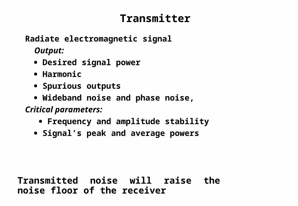
Transmitter
Radiate electromagnetic signal
Output:
Desired signal power
Harmonic
Spurious outputs
Wideband noise and phase noise,
Critical parameters:
Frequency and amplitude stability
Signal’s peak and average powers
Transmitted noise will raise the noise floor of the receiver
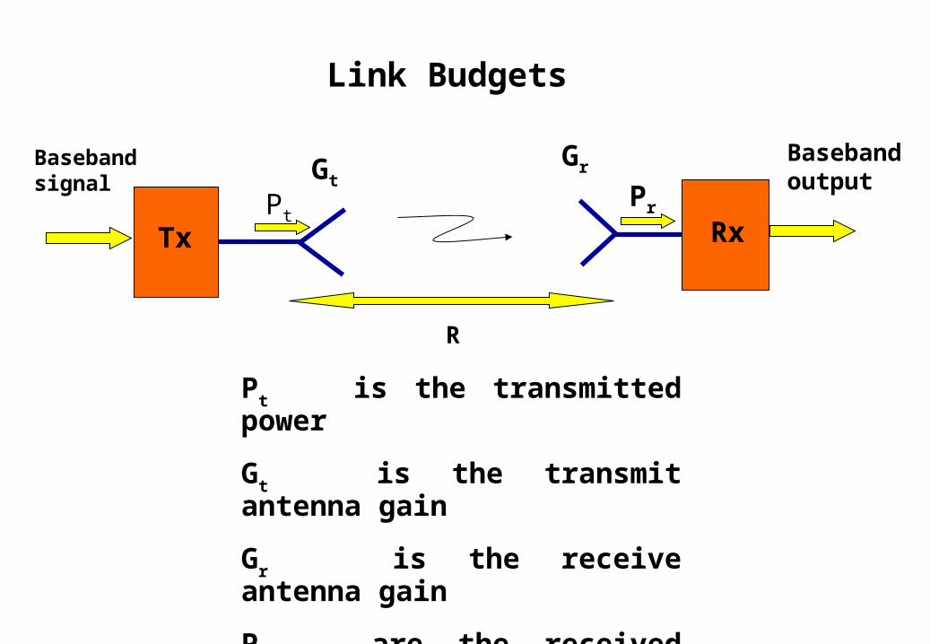
Link Budgets
Tx Rx
Baseband signal
Baseband output
R
PtPr
GtGr
Pt is the transmitted power
Gt is the transmit antenna gain
Gr is the receive antenna gain
Pr are the received power
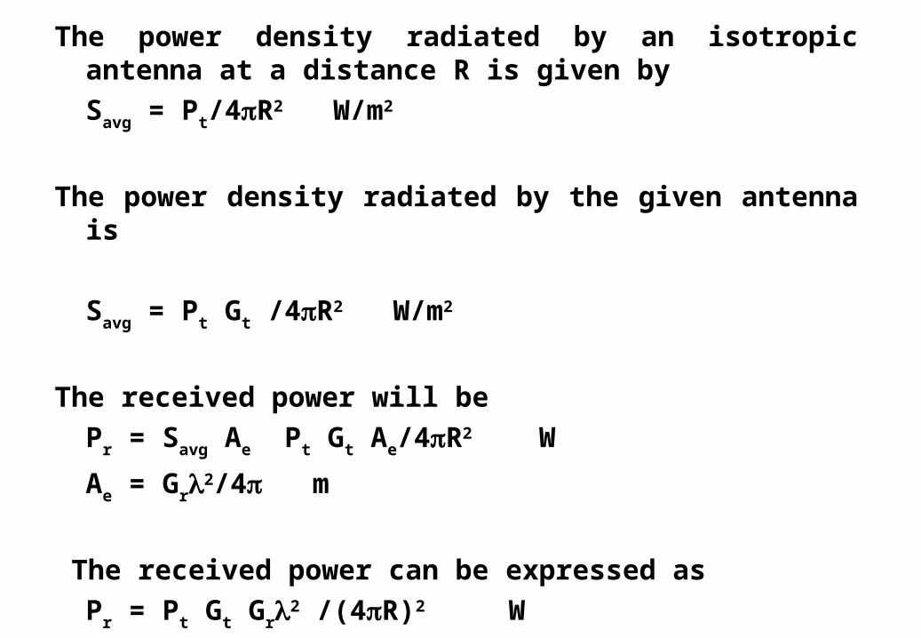
The power density radiated by an isotropic antenna at a distance R is given by
Savg = Pt/4R2 W/m2
The power density radiated by the given antenna is
Savg = Pt Gt /4R2 W/m2
The received power will be
Pr = Savg Ae Pt Gt Ae/4R2 W
Ae = Gr2/4 m
The received power can be expressed as
Pr = Pt Gt Gr2 /(4R)2 W

Pr / Ni = (Pt Gt) [2 /(4R)2] Gr / KTAB
= (Pt Gt) [2 /(4R)2] (Gr /TA)/KB
= EIRP Path loss Figure of merit / KB where,
EIRP is the equivalent isotropic radiated power
TA is the antenna noise temperature
G/T is a useful figure of merit for a receive antenna because it characterizes the total noise power delivered by the antenna to the input of a receiver.
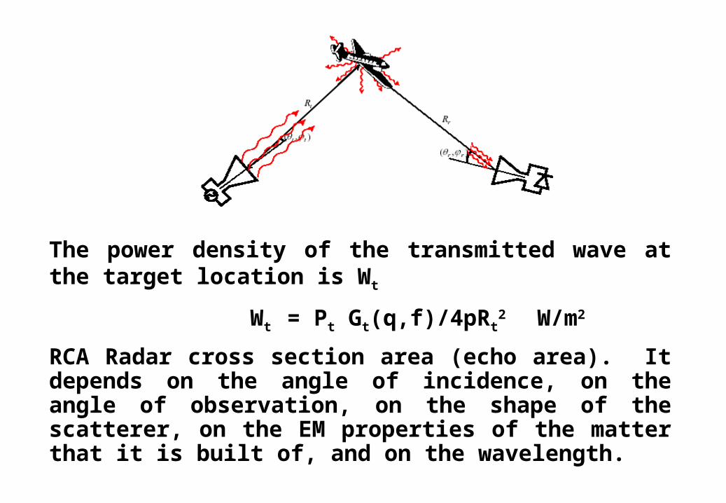
The power density of the transmitted wave at the target location is Wt
Wt = Pt Gt(q,f)/4pRt2 W/m2
RCA Radar cross section area (echo area). It depends on the angle of incidence, on the angle of observation, on the shape of the scatterer, on the EM properties of the matter that it is built of, and on the wavelength.
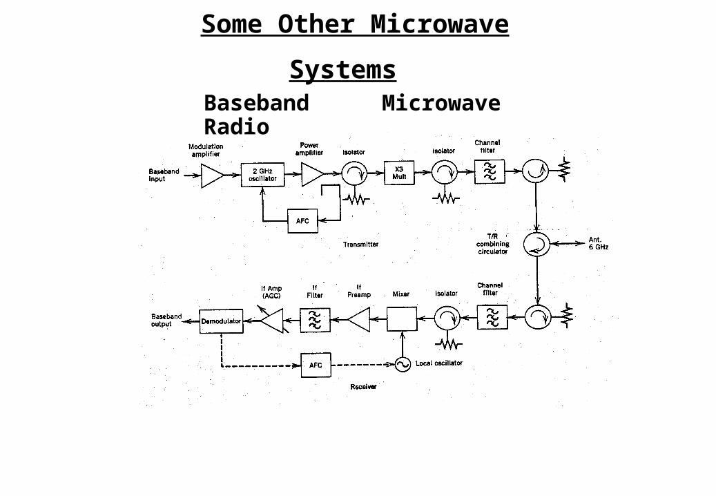
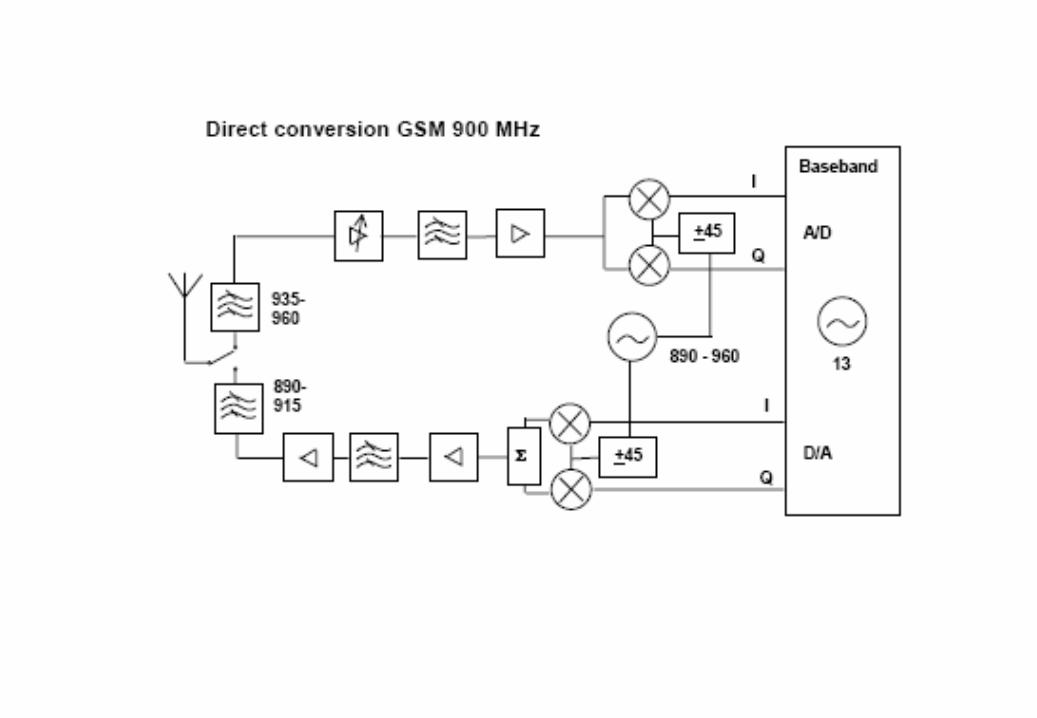
Some Other Microwave Systems Baseband Microwave Radio

RF Multiplexing technique
Baseband Repeater

Types of Microwave Devices
Passive DevicesNo DC Power & No Electronic control
Active DevicesUses DC Power or No Electronic control
Duplexers Diplexers Filters Couplers Bridges Splitters Dividers Combiners Isolators Circulators Attenuators Cables Adapters Delay lines TL
Waveguides Resonators R, L, C’s
Dielectrics Antennas
Opens, shorts, loads
Switches Multiplexers Mixers
Samplers Multipliers Diodes
Transistors Oscillators Amplifiers RFICs MICs
MMICs Modulators VCOs
VTFs VCAtten’s VCAs
Tuners Converters Synthesizer