mid project presentation
TRANSCRIPT

Adrian LangfordAdrian LangfordCommunication EngineeringCommunication Engineering
Final Year Project
Design & BuildCCD Based Optical Spectrometer

Project Aim
To design, built & test a charge-coupled-device based optical spectrometer to interrogate the 600-900nm spectrum from an optical fibre & display the results graphically in Windows

ObjectivesObjectives
Design & build the spectrometer using a diffraction grating & a Sony ILX511 2048 Pixel CCD Array
Interface the detector to the PC using an 8bit ADC, an Atmel AT90S8515 Microcontroller and 32 Kb static RAM
Develop Windows software using Microsoft Visual Basic

Realisation of a process to meet these objectives
(Refer to handout P.2)
Am
p. Spectrometer
Spread (mm)
CCDdetector
t
V
Am
p
PC VDUOpticalDispersion
Optical to electrical
conversion
Interface
Digitize, process
& buffer
Windowssoftware
Plot
PCParallel
Port
1. 2. 3. 4.

1.Spectrometer(Refer to handout P.3)
m = a(sinm sini)
Blaze angle
Direction ofblaze
Al or Aucoating
Glass substrate
a
i m
m
Diffraction grating disperses the optical input into a spectrum of constituent wavelengths
600 grooves/mm grating – each groove acts as a new source
With i = 24, min = 600nm & max = 900nm the angular spread from the grating m = 10.3

Collimation & focusing of light using a concaved mirror
Light must enter the grating as a column – light leaves grating as a column for each wavelength dispersed
Use a concaved mirror to collimate light dispersing from optical input & focus onto grating
Use a second concaved mirror to converge columns of light from grating onto unique positions along surface of detector as a function of
f
Focal point
Parallel rays
Concave mirror
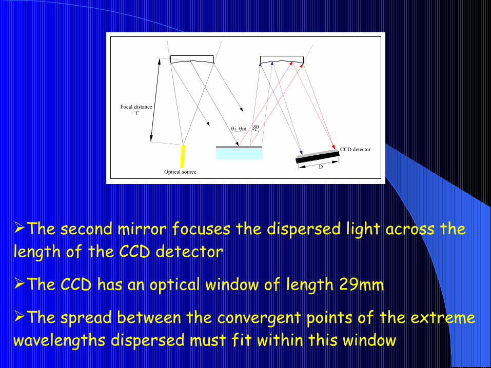
The second mirror focuses the dispersed light across the length of the CCD detector
The CCD has an optical window of length 29mm
The spread between the convergent points of the extreme wavelengths dispersed must fit within this window
i m
Optical source
CCD detector
Focal distance‘f’
D
Photon+V
Gate
SiO2
P-type
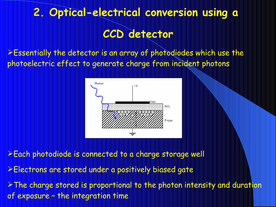
2. Optical-electrical conversion using a
CCD detectorEssentially the detector is an array of photodiodes which use the photoelectric effect to generate charge from incident photons
Each photodiode is connected to a charge storage well
Electrons are stored under a positively biased gate
The charge stored is proportional to the photon intensity and duration of exposure – the integration time

Read out
Vout
Detector array-Photodiodes-
Transport array
Pixel n Pixel 1
The CCD used, a Sony ILX511 contains 2048 pixels/photodiodes
Each rising edge of an external clock – read out gate (ROG) causes the charge collected to be transferred to a second CCD array, the transport array
Charge collected by each well is serially transferred to a single output ay 1MHz by sequentially altering gate bias voltages
Voltage appears at CCD output which varies with the charge collected by each photodiode
Weak optical signals can be enhanced by lengthening integration period
Typical integration periods – 1mS – 1S

CCD provides frames of analogue voltage variations that represent the presence of wavelengths incident along detector surface
1 read outperiod or frame
ROG
CCD Vout
Vout
CCD

Since the project objective was to plot the recovered spectrum on a PC VDU, the CCD data must first be digitised
Use an 8bit A/D converter taking samples at the CCD data rate 1MHz
The parallel port was used to get data & control signals in & out of the PC
Parallel port offers 8bit bi-directional I/O at up to 500KB/sec
Also offers a 5bit input register & 4bit output register
3. Interface
The need to buffer the CCD data
The CCD data rate is 1MHz
Using Visual Basic to access to parallel port allows a maximum I/O speed of 220KHz
Therefore the CCD data must buffered to ensure no data is lost
A 32KB static RAM FIFO buffer was used
Each frame = 2048 pixels, 8bit encoding makes each frame occupy 2.05KB
Up to 15 frames can be stored in the buffer
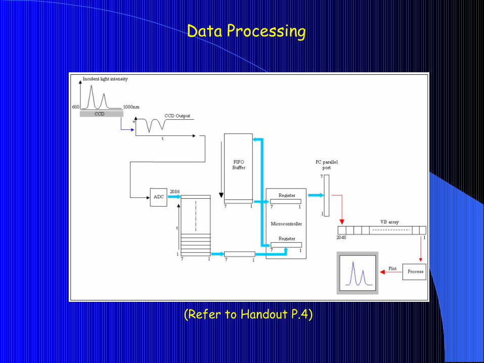
Data Processing
(Refer to Handout P.4)
Controlling the integration period
Increasing the integration period allows weak signals to be enhanced
A further requirement of the project is a means for altering the period of the ROG signal
The Windows software allows the user to choose from a range of integration periods

Controlling the ROG period
A binary pattern is presented to the parallel port corresponding to the integration period chosen by the user
The binary pattern is read by the microcontroller which pre-scales a counter accordingly
The counter toggles an output OC1B between ‘1’ & ‘0’ each time the counter reaches the pre-scale value & rolls over
The result is a pulse train output which forms the ROG signal with the users chosen period
A Langford:
Try & add a link to demonstrate varying the ROG period