mil-hdbk-978b - nasa parts application … · mil-hdbk-978-b (nasa) mil-hdbk-978b (nasa) national...
TRANSCRIPT

MIL-HDBK-978-B (NASA)
MIL-HDBK-978B (NASA)
NATIONAL AERONAUTICS AND SPACE ADMINISTRATION
NASA Parts Application Handbook
This handbook is approved for use by all elements of the National Aeronautics and Space Administration and is available for use by all departments and agencies of the Department of Defense.
Beneficial comments (recommendations, additions* deletions) and any pertinent data which may be of use in improving this document should be addressed to: Manager, NASA Parts Project Office, Goddard Space Flight Center, Greenbelt, Maryland 20771.
For user convenience this handbook was structured so that it could be separated into five volumes.

MIL-HDBK-978-B (NASA)
ii

MIL-HDBK-978-B (NASA)
FOREWORD
This handbook provides a technological baseline for parts used throughout NASA programs. The information included will improve the utilization of the NASA Standard Electrical, Electronic, and Electromechanical (EEE) Parts List (MIL-STD-975) and provide technical information to improve the selection of parts and their application, and failure analysis on all NASA projects. This handbook consists of five volumes and includes information on all parts presently included in MIL-STD-975.
This handbook (Revision B) succeeds the initial release. Revision A was not released. The con-tent in Revision B has been extensively changed from that in the initial release.

MIL-HDBK-978-B (NASA)
IV

MIL-HDBK-978-B (NASA)
CONTENTS
GENERAL CONTENTS
VOLUMES 1 through 5
VOLUME 1
Introduction Capacitors Resistors and thermistors
VOLUME 2
Diodes Transistors Microwave Devices
VOLUME 3
Microcircuits
VOLUME 4
Crystals Filters Transformers and Inductors Delay Lines Motors
VOLUME 5
Connectors, Power Connectors, Radio Frequency Protective Devices Switches Relays Wire and Cable
v
CONTENTS ^
MIL-HDBK-978-B (NASA)
THIS PAGE INTENTIONALLY LEFT BLANK
vi

MIL-HDBK-978-B (NASA)
CONTENTS
VOLUME CONTENTS
VOLUME 1
Page
Paragraph 1. INTRODUCTION - - 1-1 1.1 General - - - 1-1 1.1.1 Application handbook - - - - - - — 1-1 1.1.2 Objectives 1-1 1.1.3 Handbook organization — - - - - - - - - - - 1-2 1.1.4 Special features - - - - - — - - - - - - - - 1-2 1.1.5 Limitations - - - - - - - - - - - 1 - 3
1.2 NASA Standard parts program - - - - - - - - - 1-3 1.2.1 Standard parts program - - - - - - - - - - - - 1-3 1.2.2 MIL-STD-975 1-3
1.3 Cost - 1-4 1.3.1 Cost implication of nonstandard parts- - - - - 1-4 1.3.2 Typical basic costs 1-4 1.3.3 Additional costs - - - - - 1-4
1.4 Reliability - - - 1-6 1.4.1 Reliability prediction - - - - - - - - - - - - 1-6 1.4.2 Part count analysis - - - - — - - - - - - - 1-6 1.4.3 Part stress analysis - 1-6 1.4.4 Limitations of reliability predictions - - — 1-6
2. CAPACITORS- - 2-1 2.1 General 2-1 2.1.1 Introduction - - - - - — — — - - - - - - 2-1 2.1.2 General definitions - 2-1 2.1.3 NASA standard parts 2-3 2.1.4 General device characteristics 2-3 2.1.5 General parameter information - - - - - - - - 2-6 2.1.6 General guides and charts 2-19 2.1.7 General reliability considerations - - — — 2-22
2.2 Ceramic 2-31 2.2.1 Introduction 2-31 2.2.2 Usual applications 2-31 2.2.3 Physical construction 2-32 2.2.4 Military designation 2-36 2.2.5 Electrical characteristics 2-37 2.2.6 Environmental considerations 2-47 2.2.7 Reliability considerations - 2-47
vii
MIL-HDBK-978-B (NASA)
CONTENTS
VOLUME CONTENTS
VOLUME 1
Subject Page
2.3 Mica and glass 2-49 2.3.1 Introduction - - 2-49 2.3.2 Usual application - - - 2-49 2.3.3 Physical construction . . . 2-49 2.3.4 Military designation - 2-51 2.3.5 Electrical characteristics - - - 2-51 2.3.6 Environmental considerations - - - - - — - - 2-59 2.3.7 Reliability considerations - - - - - - - - - - 2-59
2.4 Paper and plastic - — - — - — - - 2-63 2.4.1 Introduction - - - - — - - - - - - - - — - 2-63 2.4.2 Usual applications - - — - - - — 2-63 2.4.3 Physical constructions - - - - - - — 2-64 2.4.4 Military designation - - - - — 2-67 2.4.5 Electrical characteristics - - - - - - - - - - 2-67 2.4.6 Environmental considerations - - - - - - - - - 2-72 2.4.7 Reliability considerations - - - - - - - - - - 2-73
2.5 Tantalum foil - 2-76 2.5.1 Introduction - - - - - - - - - - - - - - - - - 2-76 2.5.2 Usual applications - - - - - - - - - - - — - 2-76 2.5.3 Physical construction - - - - — - - - - - - 2-77 2.5.4 Military designation — - 2-79 2.5.5 Electrical characteristies - - - - - - - - - - 2-79 2.5.6 Environmental considerations - - - - - - - - - 2-87 2.5.7 Reliability considerations - - - — - - - - - 2-88
2.6 Solid tantalum - - 2-90 2.6.1 Introduction - - 2-90 2.6.2 Usual applications 2-90 2.6.3 Physical construction 2-90 2.6.4 Military designation 2-92 2.6.5 Electrical characteristies - - — - - - — - 2-92 2.6.6 Environmental considerations - - - - - — - - 2-103 2.6.7 Reliability considerations 2-105
vi i i

MIL-HDBK-978-B (NASA)
CONTENTS
VOLUME CONTENTS
VOLUME 1
Page
Paragraph 2.7 Wet slug tantalum - 2-107 2.7.1 Introduction - 2-107 2.7.2 Usual applications - - - — - < — 2-107 2.7.3 Physical construction 2-107 2.7.4 Military designation ^ - - - - - - - - 2-109 2.7.5 Electrical characteristics- 2-110 2.7.6 Environmental considerations - - - - 2-117 2.7.7 Reliability considerations 2-117
2.8 Variable 2-121 2.8.1 Introduction 2-121 2.8.2 Usual applications - - 2-121 2.8.3 Physical construction - — — - - 2-121 2.8.4 Military designation 2-123 2.8.5 Electrical considerations - 2-124 2.8.6 Reliability considerations 2-125
3. RESISTORS 3-1 3.1 General . . . . 3-1 3.1.1 Introduction — - - — . . . . . 3-1 3.1.2 Applicable military specifications 3-1 3.1.3 General definitions - — - - — - - - - - - 3 - 3 3.1.4 NASA standard parts 3-8 3.1.5 General device characteristics - — 3-9 3.1.6 General parameter information - - 3-11 3.1.7 General guides and charts - - 3-16 3.1.8 Prediction model 3-19
3.2 Fixed, composition (insulated)- - - - 3-22 3.2.1 Introduction - - - - - 3-22 3.2.2 Ulual applications - - 3-22 3.2.3 Physical construction 3-22 3.2.4 Military designation 3-23 3.2.5 Electrical characteristics - - 3-23 3.2.6 Environmental considerations 3-26 3.2.7 Reliability considerations 3-26
3.3 Fixed, film (high stability) 3-28 3.3.1 Introduction 3-28 3.3.2 Usual applications 3-28 3.3.3 Physical construction - - 3-28 3.3.4 Military designation 3-30 3.3.5 Electrical characteristics 3-30 3.3.6 Environmental considerations - - — - 3-31 3.3.7 Reliability considerations 3-32
i x

MIL-HDBK-978-B (NASA)
CONTENTS ^
VOLUME CONTENTS
VOLUME 1
Page
Paragraph 3.4 Fixed, film (insulated) - - 3-33 3.4.1 Introduction - - - - - - - - - - - - - - - - 3-33 3.4.2 Usual applications — 3-33 3.4.3 Physical construction 3-33 3.4.4 Military designation 3-33 3.4.5 Electrical characteristics - - - - 3 - 3 4 3.4.6 Environmental considerations - - - — - - - 3 - 3 5 3.4.7 Reliability considerations - - - - — - - - 3 - 3 5
3.5 Fixed, wirewound (accurate) 3-37 3.5.1 Introduction — — - - — 3-37 3.5.2 Usual applications - - - — - 3 - 3 7 3.5.3 Physical construction - - - - — - - 3-37 3.5.4 Military designation 3-37 3.5.5 Electrical characteristics - — - - - — - 3-39 3.5.6 Environmental considerations — - - - — - 3-39 3.5.7 Reliability considerations 3-40
3.6 Fixed, wirewound (power type) — - - - - - - 3 - 4 1 3.6.1 Introduction — - 3 - 4 1 3.6.2 Usual applications - - - - - 3-41 3.6.3 Physical construction - - - — — - - - - 3 - 4 1 3.6.4 Military designation - - - - - 3 - 4 3 3.6.5 Electrical characteristics - - - - - - 3 - 4 3 3.6.6 Environmental considerations — — - — - 3-43 3.6.7 Reliability considerations - - - - - - 3 - 4 4
3.7 Fixed, wirewound (power type, chassis mounted) 3-45 3.7.1 Introduction - - - — - - - - - - — - - - 3 - 4 5 3.7.2 Usual applications — 3-45 3.7.3 Physical construction - - - - - - - - - - - - 3-45 3.7.4 Military designation — - 3 - 4 7 3.7.5 Electrical characteristics 3-47 3.7.6 Environmental considerations — - - 3-47 3.7.7 Reliability considerations - — - - - — - 3-47
3.8 Variable, non-wirewound (adjustment type) — 3-49 3.8.1 Introduction 3-49 3.8.2 Usual applications - - - — — 3-49 3.8.3 Physical construction 3-49 3.8.4 Military designation 3 - 4 9 3.8.5 Electrical characteristics - - — - — - - 3-54 3.8.6 Environmental considerations - — — 3-54 3.8.7 Reliability considerations - - — — 3-55
x

MIL-HDBK-978-B (NASA)
CONTENTS ^
VOLUME CONTENTS
VOLUME 1
Pa^e
Paragraph 3.9 Variable, wirewound (lead screw actuated) — 3-56 3.9.1 Introduction 3-56 3.9.2 Usual applications 3-56 3.9.3 Physical construction - - — — - - - 3-56 3.9.4 Military designation - - - 3-60 3.9.5 Electrical characteristics 3-60 3.9.6 Environmental considerations - - - - - - - - 3-60 3.9.7 Reliability considerations 3-61
3.10 Fixed, film, networks 3-63 3.10.1 Introduction 3-63 3.10.2 Usual applications - — 3-63 3.10.3 Physical construction - - - — - - — - - - 3-63 3.10.4 Military designation - 3-65 3.10.5 Electrical characteristics — 3-65 3.10.6 Environmental considerations - - 3-66 3.10.7 Reliability considerations - 3-66
3.11 Thermistors (thermally sensitive resistors) - 3-68 3.11.1 Introduction 3-68 3.11.2 Usual applications 3-68 3.11.3 Physical construction 3-69 3.11.4 Military designation 3-71 3.11.5 Electrical characteristics 3-72 3.11.6 Environmental considerations — 3-72 3.11.7 Reliability considerations - - - 3-72
xi
CONTENTS ^
MIL-HDBK-978-B (NASA)
THIS PAGE INTENTIONALLY LEFT BLANK
xii
MIL-HDBK-978-B (NASA)
1. INTRODUCTION 1.1 General.
1.1.1 Application handbook. The NASA Parts Application Handbook (MIL-STD-978) has been prepared to provide a source of technical information for NASA centers and NASA contractors and to maximize standard part usage.
This handbook summarizes current technical knowledge over a broad spectrum of high reliability electrical and electronic component parts. The handbook will not only assist in resolving frequent problems involving component parts but will help avoid such problems by encouraging more knowledgeable part selection and application.
This handbook is an integral part of the NASA Standard Parts Program with MIL-STD-975, the NASA Standard Electrical, Electronic, and Electromechanical (EEE) Parts List. This handbook should not be used to select specific parts since it may, for information purposes, describe technologies which aren't listed in MIL-STD-975. Specific parts should be selected from those shown in MIL-STD-975.
1.1.2 Objectives. The extensive information in this handbook and MIL-STD-975 should make the following possible:
a. Improved product reliability and quality
b. Increased user knowledge for the selection and application of component parts
c. Improved understanding of component trade-offs
d. Improved understanding of part design and construction for use when conducting destructive physical analyses or failure analyses
e. Reduced product cost through increased standardization
f. Simplified parts procurement system
g. Simplified logistics and planning
h. Smaller parts inventory
i. Uniform incoming inspection routines
j. Improved understanding and use of the NASA Standard Parts Program.
1-1

MIL-HDBK-978- B (NASA)
1. INTRODUCTION
1.1.3 Handbook organization. This handbook is divided into five volumes. Each volume details specific components as follows:
Volume 1 Introduction Capacitors Resistors and Thermistors
Volume 2 Diodes Transistors Microwave Devices
Volume 3 Microcircuits
Volume 4 Crystals FiIters Transformers and Inductors Delay Lines Motors
Volume 5 Connectors, Power Connectors, Radio Frequency Protective Devices Switches Relays Wi re and Cable
1.1.4 Special features. This handbook discusses a full range of electrical, electronic, and electromechanical component parts. It provides extensive detailed technical information for each component part.. The following list shows some of the subjects covered:
Cost factors Screening techniques Conversion factors Standard parts Definitions Environmental considerations Construction details Selection criteria Operating characteristics Circuit application Derating Failure rates Failure mechanisms Radiation effects
The handbook is organized so that new part types and additional topics can be easily added. Consistent formats are used to ensure that specific types of information are located in the same place within each section.
The standard format used for each general section (e.g., Capacitor, general) is:
a. Introduction
. b. Definitions, abbreviations, conversion factors
1-2

MIL-HDBK-978- B (NASA)
1. INTRODUCTION
c- NASA standard parts
d. General device characteristies
e. General parameter information
f. General guides and charts
g. Reliability considerations.
The standard format used for each subsection (e.g., Capacitors, ceramic) is:
a. Introduction
b. Usual applications
c. Physical construction
d. Military designation
e. Electrical characteristics
f. Environmental considerations
g. Reliability considerations.
1.1.5 Limitations. This handbook was generated to supplement MIL-STD-975 and should not be used for individual part selection. The text often cites indi-vidual parts for explanation purposes; in such cases, these parts should not be selected unless they are listed in MIL-STD-975. Some technologies described in this handbook are not included as standard parts in MIL-STD-975. They are in-cluded here solely for information.
1.2 NASA Standard Parts Program.
1.2.1 Standard parts program. The NASA Standard Parts Program provides for the selection of standard parts (MIL-STD-975, NASA Standard Electrical, Electronic, and Electromechanical (EEE) Parts List), defines the guidelines for their use (MIL-HDBK-978 NASA Parts Application Handbook), and establishes policies and direction from the NASA Parts Project Office.
1.2.2 MIL-STD-975. MIL-STD-975 is the standard that is the foundation of the NASA Standard Parts Program. It establishes a list of standard electrical, electronic, and electromechanical parts for use in the selection, procurement, and application for flight and mission-essential ground support equipment. MIL-STD-975 serves the following purposes:
a. To provide the designer with a list of acceptable parts and the speci-fications for procuring them
1-3

MIL-HDBK-978- B (NASA)
1. INTRODUCTION
b. To reduce the quantity of part numbers used in space flight missions and mission-critical ground support applications in order to obtain the benefits of standardization.
Two levels of quality are used in this standard. Grade 2 parts are high quality government-specification-controlled parts for use in noncritical flight and nonmission-essential ground support applications. Grade 1 parts are higher quality government-specification-controlled parts intended for critical flight and mission-essential ground support applications. Parts included in this standard must have application need, technological maturity, and test or usage histories. Such requirements contribute to improved quality and reliability at lower cost with fewer delivery problems.
In addition, MIL-STD-975 includes derating criteria for the different part types. Derating is the reduction of electrical, thermal, and mechanical stresses applied to a part to decrease the degradation rate and prolong the expected life of the part. Derating increases the margin of safety between the operating stress level and the actual failure level for the part and pro-vides added protection from system anomalies unforeseen by the designer. MIL-STD-975 Appendix A contains specific derating conditions.
1.3 Cost.
1.3.1 Cost implication of nonstandard parts. In part selection for a given application, the design engineer considers the suitability of the part for the application. This includes electrical and mechanical characteristics, environmental capability, reliability, availability, purchase cost, and other evident factors. However, various intangibles, particularly in the area of cost, are frequently overlooked or afforded only cursory attention.
1.3.2 Typical basic costs. Experience has shown that typical costs involved in the specification of a new nonstandard part can range from very low for simple devices to as high as $50,000 for complex integrated circuits. This in-cludes only the basic costs of introducing a new part into inventory. The con-tribution of activities involved in the total basic cost is shown in Figure 1.
The relative contribution of each of these activities will vary among the various part types. For example, drawing preparation may be low for resistors but may be 20 times as high for complex integrated circuits. Qualification costs for an initial source can be $50,000 or more depending on the complexity of the device. Qualification of additional sources, if required, will add considerably to these costs.
1.3.3 Additional costs. Additional considerations for which costs are diffi-cult to estimate, but are still very significant, include:
a. Stocking costs including handling, storage space, storage facilities, and inventory control
1-4

MIL-HDBK-978- B (NASA)
1. INTRODUCTION
ACTIVITV
DRAWING PREPARATION
DRAWING DISTRIBUTION
DRAWING MAINTENANCE
NONSTANDARD PART APPROVAL
SOURCE QUALIFICATION
PROCUREMENT
INCOMING INSPECTION
ALTERNATE SOURCING
lO ZO 30 40
PERCENT OF TOTAL COST
FIGURE 1. Typical new part activity costs.
b. Problems entailed by having only a single source which is typical with special or nonstandard parts
c. Increased cost due to small procurement quantities; this cost is estimated to average an additional 40 percent over the purchase cost of larger quantity standard parts
d. Problems of schedule slippage, expediting, and decreased vendor re-sponse on problems with special or nonstandard parts
e. Additional failure analysis activity entailed by new, immature, or unproven parts
f. Cost of equipment repair and replacement of additional component failures entailed by use of unproven parts
g. Costs of establishing inspection procedures and providing inspection equipment for different part types; inspection costs are also in-creased because of the larger number of smaller lots of material
h. Cost of writing and developing programs for inspection of devices on automatic test equipment
i. Logistic support for maintaining supplies of the new part for field mai ntenance.
1-5

MIL-HDBK-978- B (NASA)
1. INTRODUCTION
1.4 Reliability.
1.4.1 Reliability prediction. Reliability is a consideration at all levels of electronics, from materials to operating systems, because materials make up parts, parts compose assemblies, and assemblies are combined in systems of ever increasing complexity and sophistication. Reliability engineering is concerned with the time degradation of materials, physical and electronic measurements, equipment design, processes and system analysis, and synthesis.
The primary information source for reliability prediction is MIL-HDBK-217, "Reliability Prediction of Electronic Equipment." When performing an actual reliability prediction, this handbook should be consulted. It includes for-mulas and procedures for predicting failure rates of equipment and parts. MIL-HDBK-217 emphasizes the effect of factors such as part count, part quality, environmental stresses, derating, etc. on reliability and provides the basic failure rates for different generic parts. Failure rate data has been compiled from experience and is included as the most complete source of this information. MIL-HDBK-217 includes two methods of reliability prediction, part count analysis and part stress analysis.
1.4.2 Part count analysis. This prediction method is applicable during bid proposal and early design phases. The factors impacting the reliabilty predic-tion are part technology, complexity, part count, quality levels, packaging, and application environment. This method provides a basic indication of the system potential to meet reliability goals.
1.4.3 Part stress analysis. This method is applicable when most of the design is completed and a detailed parts list including part stresses is available. It can be used for reliability trade-offs versus part selection.
The quality of the part and the application environment have a direct effect on the part failure rate. The quality levels identified in MIL-STD-975 for standard parts should be used in calculations for part reliability. The environment typically will be space flight or benign ground (for mission-essential ground support equipment).
Other factors which impact reliability predictions are power and current ratings, voltage stress, operating frequency, temperature, matching balance with networks, construction, etc. Microcircuits are treated separately with prediction models for six major classes: digital, linear, microprocessors, memories, hybrids, and converters.
1.4.4 Limitations of reliability predictions. Reliability prediction has at least two practical limitations: —
a. The ability to accumulate data of known validity for new applications
b. The complexity of the prediction techniques.
1-6
MIL-HDBK-978- B (NASA)
1. INTRODUCTION
Gathering data to provide statistically valid reliability figures requires effort and diligence. Casual data gathering accumulates data so slowly that a valid level of data may never be reached. When a number of participants gathers data, different methods and conditions are used which prevents exact coordination and correlation of the results. Part reliability data from field use of equipment is difficult to examine due to the lack of suitable data being acquired. The derivation of failure rates is empirically difficult and obtain-ing valid confidence values is practically precluded due to the lack of corre-lation.
The failure rates and their associated adjustment factors presented in MIL-HDBK-217 are based upon evaluation and analysis of the best available data at the time of issue of that handbook.
1-7
1. INTRODUCTION
MIL-HDBK-978- B (NASA)
THIS PAGE INTENTIONALLY LEFT BLANK
1-8

MIL-HDBK-978- B (NASA)
2.1 CAPACITORS, GENERAL
2. CAPACITORS
2.1 General.
2.1.1 Introduction. The following sections are intended to help the design engineer select the proper capacitor to fill a particular need. In order to select the proper capacitor, the designer requires not only a description of the device and its specification limits, but also some insight as to its advan-tages and disadvantages for a given application, peculiarities of construction, mechanical or environmental limitations, reliability, and failure modes or mechanisms.
2.1.1.1 Applicable military specifications. The applicable military specifi-cations are given in Table I and in the appropriate subsection.
2.1.2 General definitions. This paragraph defines common terms used in the rating and design application of capacitors.
Aging sensitivity. Aging sensitivity is the reduction of the useful life of a device resulting from deterioration mechanisms such as oxidation and wear.
Ambient temperature. The average or mean temperature of the medium (air, gas, liquid, etc.) surrounding a device.
Anode. The positive electrode of a capacitor.
Capacitance. The property of a capacitor which permits the storage of electri-cal energy when a given voltage is applied. Capacitance is measured in farads, microfarads, or picofarads.
Capacitance tolerance. The maximum deviation (expressed in percent) from the specified nominal value at standard (or stated) environmental conditions.
Capacitive reactance. The resistance to the flow of an alternating or pulsat-ing current by the capacitance, measured in ohms.
Capacitor. An electronic component consisting of two conducting surfaces sepa-rated by an insulating (dielectric) material. A capacitor stores electrical energy, blocks the flow of direct current and permits the flow of alternating or pulsating current to a degree dependent on the capacitance and the frequency.
Capacitor, 1 iquid-fi11ed . A capacitor in which a liquid impregnant occupies substantially a! I or the case volume not required by the capacitor element and its connections. (Space may be allowed for the expansion of the liquid with temperature variations.)
2-1

MIL-HDBK-978- B (NASA)
2.1 CAPACITORS, GENERAL
Capacitor, 1iquid-impregnated . A capacitor in which a liquid impregnant is predominantly contained within the foil and paper winding, but does not occupy all of the case volume.
Capacitor, temperature-compensating. A capacitor whose capacitance varies with temperature in a known and predictable manner.
Cathode. The negative electrode of a capacitor.
Derating. Derating is the intentional reduction of the stress-vs-strength ratio in an application of the item, for the purpose of extending its operating life.
Dielectric. The insulating material (air, paper, mica, oil, etc) between the plates of a capacitor.
Dielectric absorption. The property of an imperfect dielectric whereby all electrical charges within the body of the material caused by an electric field are not returned to the field.
Dielectric constant. The property of a dielectric material that determines how much electrostatic energy can be stored per unit volume when a unit voltage is applied. (The ratio of the capacitance of a capacitor filled with a given dielectric to that of the same capacitor with a vacuum dielectric.)
Dielectric strength. The maximum voltage that a dielectric material can with-stand without rupturing. (The dielectric strength will depend on the thickness of the material and the test method and conditions).
Dissipation Factor (DF). The ratio of resistance to reactance, measured in percent.
Electrolyte. A current-conducting solution (liquid or solid) between two elec-trodes or plates of a capacitor.
End-of-life design limit. The end-of-life design limit for devices is the expected variation in the electrical parameters of devices for which allowance must be made in circuit design. The parameter variations are expressed as a percentage change from the specified minimum and maximum values.
Equi valent series resi stance (ESR). All internal series resistances concen-trated or "lumped" at one point in the circuit and treated as one resistance.
Flashpoint of impregnant. The temperature to which the impregnant (liquid or solid) must be heated in order to give off sufficient vapor to form a flammable mixture.
2-2

MIL-HDBK-978- B (NASA)
2.1 CAPACITORS, GENERAL
Impedance (Z). The total resistance to the flow of an alternating or pulsating current, measured in ohms. (Impedance is the vector sum of the resistance and the capacitive reactance; i .e., the complex ratio of voltage to current.)
Impregnant. A substance, usually liquid, used to saturate the paper dielectric and to replace the air between its fibers. (Impregnation increases the dielec-tric strength and the dielectric constant of the capacitor.)
Insulation resistance (IR). The direct current resistance between two conduc-tors separated by an insulating material. Capacitors are commonly subjected to two insulation resistance tests. One test determines the insulation resistance from terminal to terminal; the other test determines the insulation resistance from one or more terminals to the exterior case or insulation sleeve.
Leakage, dc (DCL). A stray direct current of relatively small value which flows through the capacitor when voltage is impressed across it.
Power factor (PF). The ratio of resistance to impedance, measured in percent.
Quality factor (Q). The ratio of reactance to resistance.
Radio interference. Undesired conducted or radiated electrical disturbances, including transients, which may interfere with the operation of electrical or electronic equipment.
Ripple voltage (or current). The ac component of a unidirectional voltage or current (the ac component is small in comparison with the dc component).
Stability. The ability of a part to resist changes in characteristic values and/or coefficients.
Surge voltage/current. Transient variation in the voltage/current at a point in the circuit. A voltage of large magnitude and short duration caused by a discontinuity in the circuit.
Temperature Coefficient (TC). The change in capacitance per degree change in temperature. It may be positive, negative, or zero and is usually expressed in parts per million per degree centigrade (ppm/°C).
2.1.3 NASA standard parts. See General Section 1.1 for a complete description of the NASA Standard Parts Program. In addition to this handbook, the princi-pal elements of this program include MIL-STD-975(NASA), a standard parts list for NASA equipment.
2.1.4 General device characteristics. The relative size and cost characteris-tics of the most popular capacitor types are described in Table I. Principal applications are described in Table II.
2-3

MIL-HDBK-978- B (NASA)
2.1 CAPACITORS, GENERAL
TABLE I. Relative size and cost
Dielectric Applicable Specification
Relative Size For Equiva- 1/ lent CV Rating
Relative Cost For Equiva- 1/ lent CV Rating
Cerami c
Fixed, general] purpose J
MIL-C-123 MIL-C-39014
Small Small
High Very low
Temperature com-pensating
MIL-C-20 Small Very low
Fixed, chip MIL-C-55681 Small Low
Glass MIL-C-23269 Large Medium
Mica MIL-C-39001 Large Medium low
Paper and plastic
Metallized plastic
MIL-C-83421 Small Medium
Metallized paper MIL-C-39022 Smal 1 Medium
Tantalum electrolytic
Nonsolid MIL-C-39006 Very small Hi gh
Solid MIL-C-39003 Very small Medium
Sol id chip MIL-C-55365 Very small Medium
1/ "C" = capacitance, "V" = voltage
2-4
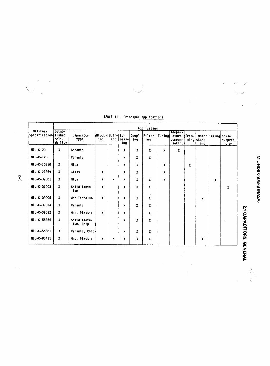
TABLE II. Principal applications
Military Specification
AD jlication Military
Specification Estab-lished reli-ability
Capacitor type
B1 ock-ing
Buff-ing
By-pass-ing
Coupl-ing
Filter-ing
Tuning Temper-ature
compen-sating
Trim-ming
Motor start-
ing
Timing Noise suppres-
sion
MIL-C-20 X Ceramic X X X X X
MIL-C-123 Ceramic X X X
MIL-C-10950 X Mica X X X X
MIL-C-23269 X Glass X X X X
MIL-C-39001 X Mica X X X X X X X
MIL-C-39003 X Solid Tanta-lum
X X X X X
MIL-C-39006 X Wet Tantalum X X X X X
MIL-C-39014 X Ceramic X X X
MIL-C-39022 X Met. Plastic X X X
MIL-C-55365 X Solid Tanta-lum, Chip
X X X
MIL-C-55681 X Ceramic, Chip X X X
MIL-C-83421 X Met. Plastic X X X X X X

MIL-HDBK-978- B (NASA)
2.1 CAPACITORS, GENERAL
2.1.5 General parameter information.
2.1.5.1 Selection. Various factors must be considered when selecting a capa citor type for a particular application. These factors are discussed below and in the subsection dealing with specific capacitor types.
a. Electrical.
Capacitance Tolerance Voltage rating AC current-carrying capacity Insulation resistance or leakage Dissipation factor or equivalent series resistance Effects of frequency Capacitance change with temperature Voltage coefficient
Dielectric absorption.
b. Mechanical.
Size Terminal configuration Mounting.
c. Environmental.
Operating temperature range Moisture resistance Shock and vibration Altitude Radiation.
d. Reliability.
Derating Failure rate Failure modes Stability Operating life.
e. Economic.
Part cost Cost of justifying nonstandard parts
Cost of samples Cost of testing Cost of negotiations with customer.
2-6

MIL-HDBK-978- B (NASA)
2.1 CAPACITORS, GENERAL
2.1.5.1.1 Important selection factors. The most important factors are dis-cussed below.
Temperature. Temperature can affect capacitance by causing variations in dielectric constant or conductor area and spacing. Temperature can also affect leakage current (through changes in specific resistance), breakdown voltage, current rating, and oil, gas, or electrolyte leakage through seals.
Humidity. Humidity can affect leakage current, breakdown voltage, power factor, or quality factor.
Barometric pressure. Barometric pressure can affect breakdown voltage and oil, gas, or electrolyte leakage through seals.
Applied voltage. Applied voltage can affect leakage current, amount of heating, dielectric Breakdown, frequency, corona, and insulation.
Vibration. Vibration can affect capacitance and integrity of the elements, terminals, or case.
Current. Current can affect internal temperature and operational life.
Life. Operating life is affected by al\ environmental and circuit conditions.
Stability. Stability is affected by all environmental and circuit conditions.
2.1.5.2 Capacitors types and their limitations.
2.1.5.2.1 Ceramic capacitors. There are two major types, NPO and BX. The NPO (negative-positive-zero) has a temperature coefficient that is effectively zero, whereas the BX type may have a capacitance change of +15 percent to -25 percent over temperature range of -55 °C to +125 °C with applied rated dc voltage. In general, the NPO has better characteristics but is larger (because of the low dielectric constant) and more expensive.
Ceramic chip capacitors are brfttle and sensitive to thermal shock. Precau-tions must be taken during mounting to avoid ceramic cracking. The substrate material should have a thermal expansion coefficient that closely matches that of the capacitors. This will help to avoid mechanical stresses that may result from changes in temperature.
The order of this listing does not necessarily imply an order of preference of an individual group.
2.1.5.2.2 Plastic film capacitors. These capacitors offer extremely tight tolerances, very low leakage currents (high insulation resistance), and minimal capacitance changes with temperature (low temperature coefficient). They are especially suited for ac applications since their extremely low dissipation factor limits the I2R heating loss.
2-7
MIL-HDBK-978- B (NASA)
2.1 CAPACITORS, GENERAL
Plastic film capacitors are limited by their relatively large size and weight and narrow range of available capacitances. Due to the nature of the dielec-tric, under certain conditions these capacitors may generate voltage transients. The voltage transients occur as a result of clearing action of pin holes in the plastic film, and electrochemical effects which cause spurious, random conduc-tion.
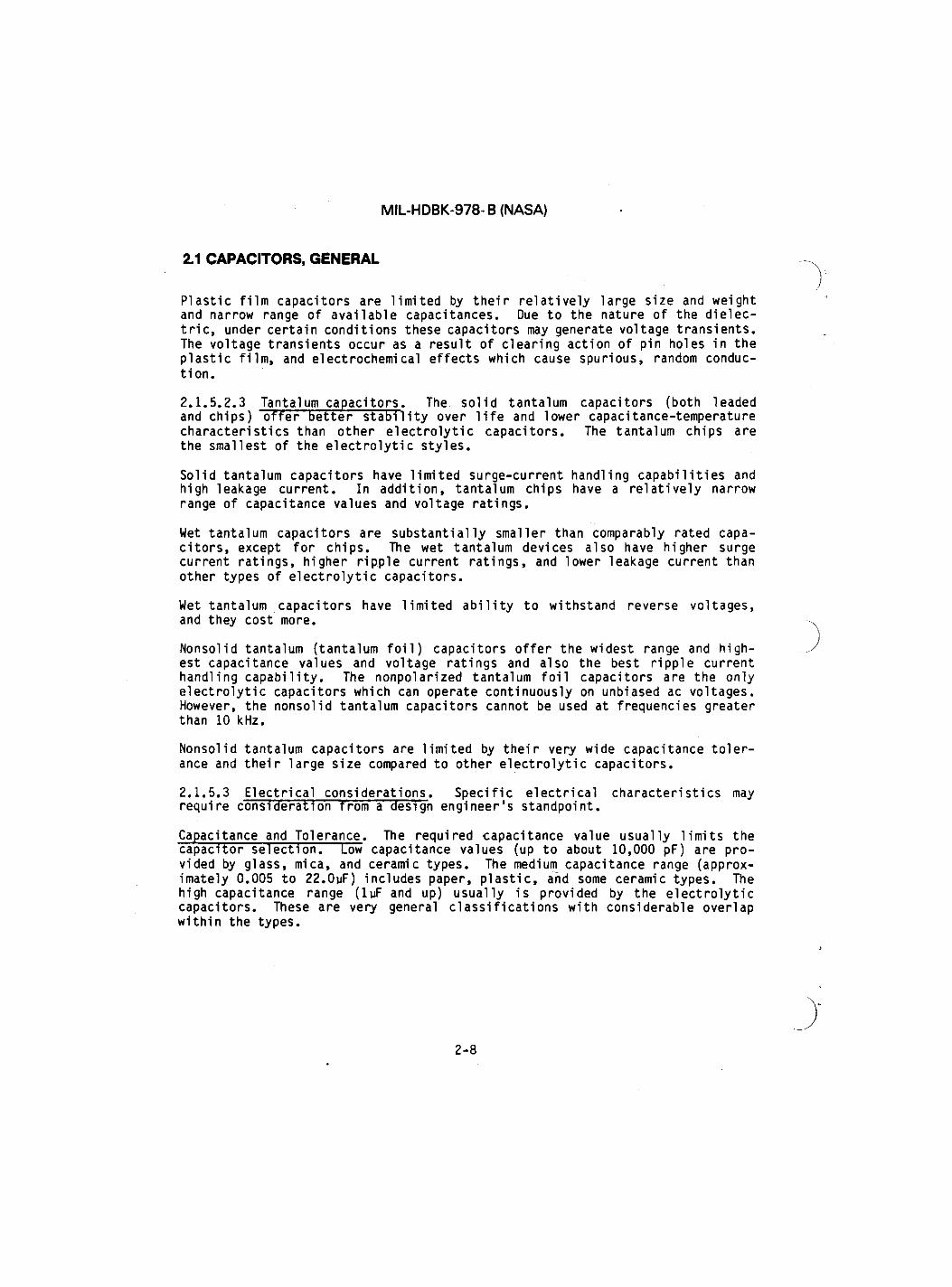
2.1.5.2.3 Tantalum capacitors. The solid tantalum capacitors (both leaded and chips) offer better stability over life and lower capacitance-temperature characteristics than other electrolytic capacitors. The tantalum chips are the smallest of the electrolytic styles.
Solid tantalum capacitors have limited surge-current handling capabilities and high leakage current. In addition, tantalum chips have a relatively narrow range of capacitance values and voltage ratings.
Wet tantalum capacitors are substantially smaller than comparably rated capa-citors, except for chips. The wet tantalum devices also have higher surge current ratings, higher ripple current ratings, and lower leakage current than other types of electrolytic capacitors.
Wet tantalum capacitors have limited ability to withstand reverse voltages, and they cost more.
Nonsolid tantalum (tantalum foil) capacitors offer the widest range and high-est capacitance values and voltage ratings and also the best ripple current handling capability. The nonpolarized tantalum foil capacitors are the only electrolytic capacitors which can operate continuously on unbiased ac voltages. However, the nonsolid tantalum capacitors cannot be used at frequencies greater than 10 kHz.
Nonsolid tantalum capacitors are limited by their very wide capacitance toler-ance and their large size compared to other electrolytic capacitors.
2.1.5.3 Electrical considerations. Specific electrical characteristies may require consideration from a design engineer's standpoint.
Capacitance and Tolerance. The required capacitance value usually limits the capacitor selection. Cow capacitance values (up to about 10,000 pF) are pro-vided by glass, mica, and ceramic types. The medium capacitance range (approx-imately 0.005 to 22.0yF) includes paper, plastic, and some ceramic types. The high capacitance range (lyF and up) usually is provided by the electrolytic capacitors. These are very general classifications with considerable overlap within the types.
2-8

MIL-HDBK-978-B (NASA)
2.1 CAPACITORS, GENERAL
Within broad limits, the availability of various capacitance tolerances is directly proportional to the absolute capacitance value. Glass and mica types are readily available in tolerances down to ±1% or less; tubular paper or plastic capacitors are normally available in the ±0.5% to ±20% range, while electrolytic capacitors are usually supplied in the range of ±5% and up, depending on the type.
Figure 1 indicates the approximate ranges of the commonly used capacitor types.
-15.+75/+5 I ELECTROLYTICS to +20
TANTALUM-FOIL AND SLUG .1 - 1200 uF)
LU
LU —I o +20/+5
TANTALUM-SOLID (.0023 - 3300 uF)
UJ oc
+20/+.25 PAPER, PLASTIC (.001 - 22 uF)
•20/+.5 pF j GP - CERAMIC (0.5 - 1.000.000)
GLASS 5 /.25 pF 1 (0.5 - 1.000.000 pF)
+10 /.5 pF MICA I (5 - 91.000 pF)
TC - CERAMIC +10 /O.l pF 1 (0.5 - 68.000 pF)
0.1 1.0 10 102 103 0.01 0.1 1.0 10 10* 103 104 10*
Capacitance and 1
2-9
MIL-HDBK-978- B (NASA)
2.1 CAPACITORS, GENERAL
Voltage rating. Figure 2 depicts typical ranges of dc voltage ratings avail-able for different dielectrics. It is important that the voltage rating of the capacitor selected be sufficiently high to allow for reliability derating, and for voltage surges or transients which may occur in the application.
TANTALUM-FOIL AND SLUG (6-450V)
TANTALUM-SOLID (6-100V) ELECTROLYTICS
PAPER - PLASTIC I (30 - 1000V)
GLASS (100 - 500 V)
I6P-CERAHIC (50 - 1600 V)
TC - CERAMIC (50 - 500 V
10 100
MAXIMUM WORKING VOLTAGE, V
1000
FIGURE 2. Maximum working voltage vs dielectric.
High voltage capacitors (1000 volts and up) must be selected with special care. Corona effects must be considered. In addition to generating spurious electri-cal signals which may impair equipment performance, corona breakdown results in deterioration of the capacitor dielectric, and can cause eventual capacitor breakdown. Corona results from voids in the dielectric/conductor layers. It is believed to cause dielectric deterioration by generating localized hot spots (dependirtg on the type of dielectric and the corona level generated). Complete dielectric breakdown may occur in a few seconds or after several thousand hours of operation. Corona is likely to occur under ac or pulse conditions.
The first step in selecting a capacitor for a given ac application is to deter-mine the voltage/current wave shape, and the ambient temperature requirements. It is especially important to know the peak voltage, the peak-to-peak voltage, and rms current, and the peak current. In the case of a pure sine wave, the information is generally straightforward. In the case of nonsinusoidal wave shapes, it is sometimes necessary to take an oscilloscope photograph. A scope trace of the capacitor wave shape is very helpful and in some cases absolutely essential to determine the required information.
2-10

MIL-HDBK-978- B (NASA)
2.1 CAPACITORS, GENERAL
AC rating. Operation of capacitors under ac conditions involves three important considerations: the dc voltage rating of the device, the internal heat rise due to I^R losses, and the corona start level.
Unless the capacitor is rated specifically for ac operation, the ac limitations of the device should be investigated. The peak value of the applied ac voltage must not exceed the dc rating of the device. The temperature rise due to inter-nal heat losses must not exceed the maximum temperature rating of the device. The current-carrying capability of different capacitor types varies widely. The general rule of thumb used by many manufacturers requires that case temperature rise be limited to 10°C.
Corona can be generated at fairly low ac voltage levels. As an example, tests on unimpregnated Mylar capacitors indicate a corona start level of 250 volts peak.
Insulation resistance. Insulation resistance (IR) is expressed in megohms or megohm-microfarads for capacitors with conventional dielectrics, and in terms of leakage current (usually microamperes) for electrolytic capacitors. The effects of this parameter may be significant in timing and coupling applications, or where the capacitor is used as a voltage divider. Leakage current increases with temperature. Figure 3 shows typical values for various dielectric mater-ials.
FIGURE 3. Typical values of insulation resistance vs temperature.
2-11

MIL-HDBK-978- B (NASA)
2.1 CAPACITORS, GENERAL
Dissipation factor (DF) or equivalent series resistance (ESR). The dissipation factor is a function of capacitance, ESR, and frequency. Unless otherwise specified, DF is measured at the following frequencies:
1 MHz for C < 100 pF 1 kHz for 100 pF < C 120 Hz for electrolytic capacitors
DF may vary widely with temperature and to a great extent for ceramic and elec-trolytic capacitors.
Frequency effects. Most basic capacitor parameter formulas include a frequency term. Capacitor characteristics are to some extent affected by frequency. All capacitors have some inductance associated with their conductors and therefore will resonate at some frequency.
Figure 4 illustrates simplified equivalent circuit of a capacitor wherein all distributed parameters are shown as "lumped" values.
Rp
T Q V A n r y y \ Rs L
FIGURE 4. Equivalent circuit of a capacitor.
Under dc or low frequency conditions, Rs and L are negligible compared to the C and Rp combination. As the frequency increases, particularly to the megahertz range, both R$ and L increase. Rs increases due to a "skin effect" (where the current tends to travel only through the outer surface metal of a conductor under high frequency conditions). This appears as an increase in the resistance of the conductor. L increases due to the action of the ac current flowing in the leads, electrodes, and terminals, thus generating a magnetic field around them proportional to the frequency.
Since the dielectric constant of most materials will vary with frequency, capacitance is also affected by frequency.
Further examination of the impedance equation shows that as the frequency increases, XQ tends to decrease while X|_ increases in value. This means that
2-12
MIL-HDBK-978- B (NASA)
2.1 CAPACITORS, GENERAL
the (Xc-XL)2 term decreases until at some frequency, the term (XQ-X[_)^ will equal zGro and disappear. Then Z = R$ and the capacitor will resonate. This is the point where the capacitor appears as a Dure resistor in the circuit.
It also follows that if a capacitor is operated at a frequency higher than its resonant frequency, it will no longer function as a capacitor in the circuit, but will appear as an inductor.
As there are so many variables affected by frequency, no attempt will be made here to present comparative values. As a guide for general frequency applica-tions for different types of capacitors, Figure 5 can be used for an initial approximation. Specific computations or measurements should be implemented to finalize any particular •application. Figure 5 reflects frequency ranges for the most efficient application based on normal design values and criteria. Both the upper and lower limits of the frequency range can be extended by special design and construction techniques, as shown by the dashed areas.
FREQUENCY APPLICATION RANGE (STANDARD DESIGNS)
POLYSTYRENE, TEFLON, POLYCARBONATE
i LOW-LOSS CERAMIC
c : : i m m s s m s s ^ i
i LOW-LOSS CERAMIC
c : : i m m s s m s s ^ i
MYLAR
H K CERAMIC
[ i m w w i i
MYLAR
H K CERAMIC
[ i m w w i i PAPER
i m s \ s \ \ \ \ \ \ \ \ H : : : :
TA ELECT
1 1 1 1 1 I I I 1 I 1 o 101 to 2 103 104 105 106 107 10®
FREQUENCY (Hz) 109 1010
FIGURE 5. Frequency application range (standard designs).
2-13

MIL-HDBK-978- B (NASA)
2.1 CAPACITORS, GENERAL
Temperature effects. Temperature variations (which affect the dielectric con-stant of capacitor material) result in capacitance changes (AC) that can vary from minor to major.
Figures 6 and 7 compare typical temperature coefficient curves of commonly used dielectric types. It should be noted that the curves shown in Figure 7 are for nonimpregnated capacitors. Plastic film capacitors cannot be impregnated and the impregnant (or filler) serves mainly to replace part of the air film. The resultant dielectric constant will vary slightly, thus altering the temperature coefficient curve proportionately.
Voltage coefficient. Capacitance variation with applied voltage is insignifi-cant except with Class II (general purpose) ceramics. High K dielectrics are ferroelectric in nature, and their molecular orientation varies with dielectric stress. See the ceramic subsection for further details.
Dielectric absorption. This phenomenon is due to the tendency of the dielec-tric to retain electrons it has stored when the capacitor is discharged. When the shorting mechanism is removed, the electrons that remained in the dielec-tric will eventually accumulate on an electrode and cause a "recovery voltage" gradient to appear across the capacitor terminals. This recovery voltage, divided by the charging voltage and expressed as a percent figure, is called the "percent dielectric absorption."
The magnitude of this percent dielectric absorption figure will vary consider-ably for different dielectric materials and their impregnants. It is important to note that the measured value of dielectric absorption is a function of the amplitude of the charging voltage, the charging time, the discharge time, the time after discharge that measurements are made, and the temperature.
This tendency of the dielectric to retain its electrons is primarily due to the polarization that takes place at the dielectric dipoles whenever the capa-citor is energized. These electrons, in effect, become "bound" or trapped in the dielectric during the discharge period. When the shorting mechanism is removed, these electrons become free again and move to the electrode surface. This results in a potential difference between the electrodes (the "recovery voltage").
A second factor in the magnitude of recovery voltage values is the random move-ment of "free" electrons in the dielectric. These free electrons take a finite time to move from the dielectric to the electrode, and therefore contribute to the recovery voltage. The magnitude of their contribution is closely related to the discharge time duration.
2-14

MIL-HDBK-978- B (NASA)
2.1 CAPACITORS, GENERAL
I T V P I C A L V A L U E S OF DRY SECTIONS)
P O L Y C A R B O N A T E ( A ) >
P O L Y C A R B O N A T E (B) V
T E F L O N
P O L Y S T Y R E N E
M Y L A R
/
/ 7
P O L Y C A R B O N A T E
M Y L A R
-10 25 35 so es T E M P E R A T U R E <°C»
125
FIGURE 6. Film dielectric capacitance vs temperature,
2S 35 50 TEMPERATURE (°C»
125
FIGURE 7. Capacitance vs temperature (typical).
2-15

MIL-HDBK-978- B (NASA)
2.1 CAPACITORS, GENERAL
Table III shows approximate percent value of dielectric absorption (DA) for some typical dielectrics. These values are for a given set of conditions. A change in any of the conditions will cause a variation in the percent dielectric absorption.
TABLE III. Dielectric absorption
Conditions: Charging voltage: 200 Vdc Charging, time: 1 minute Discharge time: 2 seconds Time after discharge: 1 minute Temperature: 25°C
Dielectric % DA
Ai r 0
•Polystyrene 0.02
•Teflon 0.02
•Polycarbonate 0.08
•Mylar 0.20
Mica (ruby) 0.70
Paper (oil-impregnated) 2.0
*The addition of an oil impregnant will cause the percent DA figure to become essentially that of the impreg-nant (approximately 2.0 for most oils).
Dielectric absorption is a critical factor in circuttry that is highly depen-dent upon the speed of response or time delays in the charge and discharge cycles of a pulse circuit.
2.1.5.4 Mechanical considerations. Specific capacitor design characteristics may require special consideration from a product design standpoint.
Mounting by leads. While specifications require that components weighing more than one-half ounce may not be mounted only by their leads, it does not follow that lead-only mounting is satisfactory for all components weighing less than one-half ounce. Nearly all capacitor specifications require rigid mounting of the body during vibration tests.
2-16

MIL-HDBK-978- B (NASA)
2.1 CAPACITORS, GENERAL
Encapsulation. Potting with a hard epoxy can cause capacitor failure by shorting the dielectric as a result of differential pressures exerted after hardening. Solid tantalum capacitors are subject to failure by shorting when potted, and require a buffer coating to prevent internal shorting.
2.1.5.5 Environmental considerations. The behavior and service life of all capacitors are highly dependent upon the environments to which they are exposed. The following is a summary of the environmental factors that are most critical in their effect on capacitors. The design engineer should take into account individual environmental factors as well as combinations of these factors.
Ambient temperature. The temperature of the immediate space surrounding the capacitor is of critical importance since this is one of the factors that determines the temperature at which the dielectric operates.
Service life. The service life of a capacitor will decrease with increased temperature. Another factor affecting service life is dielectric degradation resulting from chemical activity with time.
Capacitance. Capacitance will vary with temperature depending on the dielec-tric and construction. Both the dielectric constant of the material and the spacing between the electrodes may be affected. These effects may reinforce or cancel each other.
Insulation resistance. The insulation resistance decreases with increased temperature due to increased electron mobility.
Dissipation factor. The dissipation factor is a complex function of tempera-ture and may vary up or down with increased temperature depending on the di-electric material.
Dielectric strength. The dielectric strength (breakdown voltage stress level) decreases with increased temperature. As temperature increases, the chemical activity increases; this will cause a change in the physical or electrical properties of the dielectric.
Sealing. For sealed capacitors, increased temperature results in increased internal pressure that can rupture the seal and result in impregnant leakage and moisture susceptibility.
Humidity (moisture). Moisture absorption by a capacitor can cause parametric changes, reduced service life, and in some cases, early life failures if mois-ture penetration is sufficient. The most noticeable effect is a decrease in insulation resistance.
The ability of various nonhermetically sealed capacitors types to withstand moist environments is of considerable interest to component or design engineers faced with miniaturization requirements. Generally the nonhermetic unit is con-
2-17
MIL-HDBK-978- B (NASA)
2.1 CAPACITORS, GENERAL
siderably smaller than an equivalent hermetically sealed unit. Most military capacitor specifications require exposure to the moisture tests listed below. Details of test conditions and post-test limits are called out in the individual capacitor specifications.
a. Immersion cycling. This is a test in which the capacitors are immersed for two or more cycles in fresh or salt water for a period of 15 to 60 minutes per cycle.
b. Moisture resistance. This test uses a combination of temperature cycling and humidity exposure for 10 cycles, each cycle lasting 24 hours. Subzero temperature exposure and vibration are also included in the cycling phase.
In any nonhermetic unit such as the plastic case or the plastic wrap-epoxy end-filled type of capacitor, moisture can penetrate through the epoxy and plastic casing. The amount of moisture that penetrates will depend on the time, the integrity of the bonding junction between the epoxy and the lead, the density of the plastic material, and the thickness of the epoxy/plastic material.
A distinction should be made between paper and plastic film dielectric designs. Nonhermetic capacitor designs that "use paper for all or part of the dielectric are much more vulnerable to moisture than designs using plastic film as a di-electric. Once moisture vapor has penetrated into the dielectric, the paper will absorb the moisture, trapping it and eventually destroying the insulating properties of the paper. For this reason, military equipment specifications disallow the use of paper or paper-plastic dielectrics in other than hermetical-ly sealed metallic cases. In the case of the film dielectric, there is practi-cally no absorption of the vapor by the film and it will either be cycled back out of the capacitor or remain in the air space next to the film surface. While the vapor is in the capacitor, it causes a degradation in the insulation resis-tance properties of the capacitor. Usually, however, the insulation resistance value of the film dielectric capacitor with moisture vapor present is still superior to that of the paper dielectric capacitor with absorbed moisture.
Vibration, shock, and acceleration. A capacitor can be mechanically destroyed or damaged or may malfunction if it is not designed and manufactured to with-stand vibration, shock, or acceleration conditions present in the application. Movement of the internal assembly inside the container can cause capacitance changes, dielectric or insulation failures due to physical movement of the elec-trode foils or internal roll connections, and fatigue failures of the terminal connections. In addition, external terminals, the case, and mounting brackets, are subject to mechanical stress distortion. Some ceramic capacitors also exhibit a piezoelectric effect which may be a problem in critical circuitry.
Barometric pressure. The altitude at which hermetically sealed capacitors are to operate will affect the voltage rating of the capacitor terminals. As barometric pressure decreases, the ability of the terminal to withstand voltage arc-over also decreases.
2-18

MIL-HDBK-978- B (NASA)
2.1 CAPACITORS, GENERAL
For liquid-impregnated capacitors, the differential between the internal and external pressure becomes greater when the external pressure is reduced. This puts added stress on the seams and terminal seals and can result in rupture of the hermetic seal and impregnant leakage.
Capacitance can be affected by internal dimensional changes due to pressure differentials, and internal arc-overs can result when a partial vacuum condi-tion exists in.the capacitor.
Heat transfer by convection is decreased as altitude is increased. This con-dition must be evaluated in cases where the application results in heat gener-ation within the capacitor.
2.1.6 General guides and charts.
2.1.6.1 Capacitor formulas.
Capacitance. Capacitance is a measure of the quantity of electrical charge per unit of voltage differential that can be stored between electrodes (Figure 8).
AREA (A)
DIELECTRIC MATERIAL WITH DIELECTRIC CONSTANT <K)
FIGURE l. Capacitor formulas.
(N-l) A x 10-12 C « 0.224K J 1 — - — farads
d
where A = area of one side of one plate in square inches N = number of plates d = distance between plates in inches K = dielectric constant
C « KA/d
Table IV is a chart of various dielectric materials and their dielectric con-stants. The approximate («) sign is used rather than an equal sign because these dielectric constants vary somewhat with purity, temperature, frequency, voltage, treatment during manufacture, and various other factors.
2-19

MIL-HDBK-978-B (NASA)
2.1 CAPACITORS, GENERAL
TABLE IV. Dielectric constants at +25°C
Dielectric Material (K) Dielectric Constant
Vacuum 1.0 Air 1.0001 Teflon a 2.0
Polystyrene S3 2.5 Polycarbonate a 2.7 Mylar ' « 3.0
Polyethylene a 3.3 Kraft paper tst 2.0 to 6.0 Mica w 6.8
Aluminum oxide n 7.0 Tantalum oxide m 11.0 Ceramics BS 35.0 to 6,000 +
Dissipation factor, power factor, and Q. Each of these terms can be used to express how far a capacitor deviates from being a pure circuit element (see Figure 9).
Capacitor equivalent circuit
Vector relationships
FIGURE 9. Capacitor equivalent and vector relationship.
2-20

MIL-HDBK-978-B (NASA)
2.1 CAPACITORS, GENERAL
where R = effective series resistance in ohms.
XL = 2irf L = uL = inductive reactance in ohms.
Xr = 1 = 1 = capacitive reactance in ohms 7 W T d T
Z = R 2 + (Xc - XL)2 = impedance in ohms.
0 = phase angle between current and voltage.
RS = shunt leakage resistance (negligible for these calculations),
f = frequency in Hertz,
a) = 2irf s frequency in radians per second.
Ohm's Law gives the following: Ez = III; Ec = ICXCJ ER = IrR
and power equations give: Total volt-amperes = I^^z = Iz2Z * I2Z
Reactive volt-amperes - IQEc = I C2X C = I2XC
Resistive VA (watts) = IRER = I r2R = I2R RLR
therefore PF = P(in)-P(out) = jjk = i = cos e
P(in) 12Z Z
and DF is defined as the ratio of resistance to reactance,
DF = R = cot (0)
XC
Note that for "good" capacitors
R and Xl are << Xq such that Z 2 = R 2 + (XC-XL)2 = X c2 and since Z s Xc
PF = R s R_ = DF Z XC
Q (figure of merit) is defined as the ratio of reactance to resistance:
Q = XC _ 1 . 1 T ~ W = W
FIGURE 9. (Continued).
2-21

MIL-HDBK-978- B (NASA)
2.1 CAPACITORS, GENERAL
2.1.7 General reliability considerations.
2.1.7.1 Established reliability parts. A large percentage of military type capacitors are available as "established reliability" (ER) parts. Capacitors procured to these specifications have been subjected to special process con-trols and lot acceptance testing, along with 100% screening and extended life test. This includes an operating voltage conditioning for level "S" parts or better. Level MSM corresponds to a guaranteed failure rate of no more than 0.001%/1000 hrs at 60% or better confidence level under maximum rated operat-ing conditions. The actual failure rate under normal use conditions will be considerably less.
2.1.7.2 Use of accelerated testing techniques on capacitors (Weibull). There are several reasons for using accelerated testing in establishing useful reasons for operating life characteristics (beyond 10,000 hours) and verifying product life characteristics. The Weibull technique shows that by accelerating the stress ratio, it is possible to infer factors such as length of life, optimal sampling techniques, access failure rate level, effectiveness of manufacturing processes and quality control. It is also believed to establish more realistic failure rate computations, which represent critical information for design engineers. Level "B" corresponds to 0.1%/1000 hrs, "C" to 0.01%/1000 hrs, "D" to 0.001%/ 1000 hrs, and "E" to 0.0001%/1000 hrs. A Weibull sample can be taken at incoming inspection and the actual "real" failure rate can be compared to that claimed by a vendor.
2.1.7.3 Capacitor failure modes. Capacitors usually fail in one of the follow-ing modes:
open short intermittent low Insulation resistance capacitance drift high leakage current (for electrolytic capacitors).
Probable failure modes vary with the type of capacitor. Consult the subsection on individual types for more detailed discussion of failure modes.
2.1.7.4 Failure mechanisms. The classic capacitor failure mechanism is dielec-tric breaTHowru Assuming operation at or beneath maximum rated conditions, most dielectric materials gradually deteriorate with time and temperature to the point of eventual failure. This presumes the early elimination by inspection and screening techniques of infant mortality due to manufacturing defects or mistreatment.
In actual practice the failure mechanisms depend on the construction and type of dielectric and other materials used. More detailed discussions of failure mechanisms are listed under the applicable subsections.
2-22

MIL-HDBK-978- B (NASA)
2.1 CAPACITORS, GENERAL
2.1.7.5 Derating. With the exception of failures due to "random" occurrences resulting from manufacturing defects or overstress, capacitor failure rate is a function of time, temperature, and voltage. Operational life can be signifi-cantly lengthened by voltage derating and by limiting the operating amhient temperature.
The extent to which electrical stress (e.g., voltage, current, power) is derated depends upon temperature. The general interrelationship between electrical stress and temperature is shown in Figure 10. The approved operating conditions lie within the area below the derated limitation line (ESdr). Operation at con-ditions between the derated limitation line and the maximum specification curves results in lower reliability (see Handbook 217). Operation in this reduced reliability area requires specific approval.
The derated voltage is voltage.
the sum of the peak ac voltage and the dc polarizing
Numerical values are applied to the curves for each part type, based on a per-centage of the device manufacturer's maximum rated values. The applicable derating curve or derating percentages are specified in MIL-STP-975.
100%
00 oo Cd J— 00
< o en I— o
ESdr
PROHIBITED USE
APPROVED USE
where
TCI
CASE TEMPERATURE
case temperature above which electrical stress must be reduced maximum allowable case temperature maximum case temperature for derated operation maximum electrical stress (e.g.,voltage, power, current)
for derated operation 100% « maximum rated value per the detail specification.
Tdr ESdr
FIGURE 10. Stress-temperature derating scheme,
2-23
MIL-HDBK-978- B (NASA)
2.1 CAPACITORS, GENERAL
End-of-life limits. Circuits shall be designed such that required functional performance is maintained within the identified end-of-life design limits. The end-of-life limit may be assumed to be a 10-year period when the parts are in the approved application region (see Figure 10). The end-of-life values given in the detailed requirements section for each part type are percentage changes from initial values.
Voltage acceleration factor. In essence, if a capacitor is operated for a certain time period at some voltage stress level 1, the voltage acceleration factor can be used to equate this time of operation at voltage (Ei) to an equivalent time at some other voltage (£2). The formula for this "Voltage Power Law" is shown below.
Voltage Power Law (constant temperature)
(L}/L2) = ( E2/ El) n w h e r e : - voltage at Condition 1 Ll = 1ife at Ei E2 = voltage at Condition 2 L2 = 1ife at E2 n = proper exponent for the dielectric material and
voltage stress area under consideration.
The expression (E2/E^)n is the acceleration factor, and its accuracy depends upon the proper determination of the exponent n. This value of n will vary for different dielectric materials. It is also affected by design, processing, and test conditions. With all other considerations being equal, operating life or reliability will follow this voltage power law quite closely.
The main problem is to determine the proper value of n for specific dielectrics over specific voltage stress values. Values of n have been empirically deter-mined for various capacitor types, and that these values generally range from about 2 to 6, depending upon the type of unit and the range of stress level.
Typical values which show the variation of the exponent with the stress ratio are listed below:
n = 5 for application of 140% to 100% of rated voltage
n = 3 for application of 100% to 50% of rated voltage
n = 2 for application of 50% to 25% of rated voltage.
Thus, operation at 50% of rated voltage improves the failure rate by a factor of the voltage ratio when compared with operation at maximum rated voltage (n = 2 and 3, respectively).
2-24

MIL-HDBK-978- B (NASA)
2.1 CAPACITORS, GENERAL
Temperature acceleration factor. The temperature acceleration factor is some-what similar in concept to the voltage factor. It is based on a chemical activ-ity rule that states, "For every 10°C increase in temperature, capacitor life expectancy will be cut in half."
This statement, if accepted literally, would mean that the life expectancy of the capacitor would double for a 10°C reduction in temperature, whether from 125°C to 115°e or 35° to 25°C. Again, this is a variable exponent depending on the stress area concerned.
Temperature Rule (constant voltage)
life at Ti life at T2 (T2-Ti)/n temp at condition 1 temp at condition 2 °C rule applicable for the temperature stress area under consideration
Note: The expression on the right of the equation is the acceleration factor for the temperature, where n varies according to the dielectric and the tem-perature stress areas concerned.
2.1.7.6 Capacitor failure rate model . Various types of capacitors require different failure rate models that vary to some degree. To perform an actual reliability prediction, MIL-HDBK-217 should be used.
2.1.7.7 Radiation effects. The principal radiation effects in insulating materials (both organic and inorganic) are related to the ionization dose pro-duced by the particle or photon. The major changes in the macroscopic proper-ties (thermal, mechanical, electrical, and optical) of insulating materials resulting from ionizing radiation are: increase of ionic conductivity and di-electric loss, resulting in decrease of the dielectric Q; changes in dimensions; modification of tensile strength, yield point, and plastic and elastic proper-ties; gas evolution; small changes in the dielectric constant and dielectric strength; and increased optical absorption. Usually the predominant radiation degradation of inorganic materials results from increased conductivity of the material, whereas for organic materials, mechanical changes are usually the major effects. Mechanical changes in organic material occur because of modi-fication of the organic polymer structure caused by radical interaction and formation.
Table V summarizes the radiation resistance properties of various dielectric materials used in making capacitors. It is based on the physical changes taking place and should be used as a guide only. Data based on electrical degradation levels may or may not support the conclusions shown.
(L1/L2) = 2 m where Lj = L2 = m = Tl = T2 = n =
2-25
MIL-HDBK-978- B (NASA)
2.1 CAPACITORS, GENERAL
TABLE V. Dielectric radiation resistance chart
Material Absorbed Energy Level For Approx. 25% Degradation
Ceramics Glass Mica Polystyrene Polycarbonate Mylar Polyethylene Cellulose acetate Teflon Electrolytic* Oil-filled capa-
citors
Highly resistant (no levels given) Highly resistant (no levels given) Highly resistant (no levels given) Over 1 x 10⁹ rads Approx. 2 x 10⁸ rads Approx. 1 x 10⁸ rads 9.3 x 10⁷ rads 1.9 x 10? rads 1 x 10⁵ rads Very susceptible (no values given) Very susceptible (no values given)
*Not including solid slug tantalum
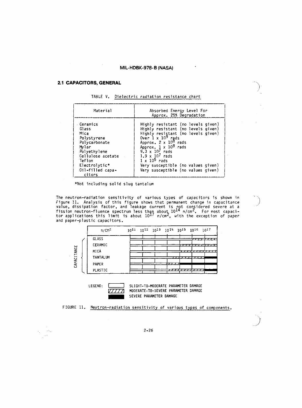
The neutron-radiation sensitivity of various types of capacitors is shown in Figure 11. Analysis of this figure shows that permanent change in capacitance value, dissipation factor, and leakage current is not considered severe at a fission neutron-fluence spectrum less than about 10*4 n/cm^. For most capaci-tor applications this limit is about 10*' n/cms with the exception of paper and paper-plastic capacitors.
N/CM2 1! 0ll 1012 10i3 101<* li 1 1 i
015 ! 01S 1017
GLASS CERAMIC MICA TANTALUM
PAPER PLASTIC
1 I I ,,,,,,, GLASS CERAMIC MICA TANTALUM
PAPER PLASTIC
GLASS CERAMIC MICA TANTALUM
PAPER PLASTIC
GLASS CERAMIC MICA TANTALUM
PAPER PLASTIC
GLASS CERAMIC MICA TANTALUM
PAPER PLASTIC
GLASS CERAMIC MICA TANTALUM
PAPER PLASTIC
GLASS CERAMIC MICA TANTALUM
PAPER PLASTIC i i iy ' '
1 i 1 " ™
LEGEND: 1 1 S L I G H T - T O - M O D E R A T E PARAMETER DAMAGE
I / / / / / I M O D E R A T E - T O - S E V E R E PARAMETER DAMAGE
S E V E R E PARAMETER DAMAGE
FIGURE 11. Neutron-radiation sensitivity of various types of components,
2-26
MIL-HDBK-978- B (NASA)
2.1 CAPACITORS, GENERAL
The principal cause of radiation-induced capacitance changes is dimensional change in the interelectrode spacing due to gas evolution and swelling. This change is more pronounced in organic-dielectric capacitor construction. Gamma heating and changes in dielectric constants of capacitor dielectrics have been rare and can be considered a second-order effect especially for inorganic materials. Normally, capacitors using organic materials such as polystyrene, polyethylene terephthalate (Mylar), and polyethylene are less satisfactory in a radiation environment by a factor of about 10 than those using inorganic dielectrics. However, it should be noted that even for these types, experimen-tal data indicate no significant permanent changes occurred for exposures up to about 1012/cm2. On the other hand, usage of tantalum and aluminum electrolytic capacitors indicates that both types show capability of surviving extended radiation exposure, with the tantalum being more radiation-resistant. Roth decreases and increases in capacitance value have been observed. For example, changes from -10 to +25 percent for tantalum have been observed for exposure up to 10*' n / c m 2 . These changes were observed during radiation exposure, with some recovery in the electrical characteristics noted within several days after the end of the radiation exposure. This recovery in some cases was rather slow, and in many instances complete recovery was never attained.
The use of wet-electrolyte capacitors is not normally permitted in high-reliability equipment. Permanent changes in electrical characteristics of these capacitors begin at about 5 x 10¹³- n/cm^. The principal mechanism is gas evolution caused by the interaction of the ionizing radiation with the electro-lyte, which tends to rupture the capacitor.
Radiation-hardening techniques. In selecting capacitors for a radiation-environment application, a survey of available component part radiation data should be performed to determine whether radiation data exist on that particular part or a similar part. If no data exist, a radiation analysis should be made of the materials that make up the capacitor to try to reduce the number of candidate parts. A radiation exposure is then performed on a few samples of the remaining candidate parts to reduce their population to one or two. These remaining candidate parts then receive extensive investigation in terms of radiation characterization. However, after a capacitor becomes qualified to a nuclear environment, there is always the problem of maintaining this nuclear qualification in any future procurement (i.e., lot-to-lot radiation-quality assurance). In reality, manufacturing processes do change and the vendor does not always inform the procuring agency. Depending on the criticality of the application, some type of screening for usage in radiation environment may have to be performed. This can vary from confirming that there was no change in manufacturing techniques to electrical screening to lot-to-lot sample radiation or to 100 percent radiation screening.
Hardening for fast neutrons. For neutron fluence less than about 10*d n / c m 2
(generally the maximum level most semiconductors devices can survive), changes in capacitance value, dissipation factor, and leakage resistance are considered to be minimum if at all detectable. For some capacitors, a fast-neutron fluence
2-27

MIL-HDBK-978- B (NASA)
2.1 CAPACITORS, GENERAL
of about 1017 n/cm2 is necessary before the radiation damage becomes severe. Glass, ceramic, mica, and tantalum are quite radiation-resistant, and they are preferred in that order. Normally, the radiation deterioration of organic dielectric materials is more severe than that of inorganic.
Ceramic, glass or tantalum dielectric material improves the capacitor radiation resistance over paper-dielectric capacitors. In order to minimize radiation effects, the capacitor voltage change, dc voltage and capacitor working voltage should be kept low. Where possible, Zener diodes should be substituted for capacitors in voltage-blocking applications. The utilization of transistor constant-current generators to supply emitter bias rather than emitter bypass capacitors is recommended.
In low-voltage tantalum-capacitor applications (i.e., when the maximum applied voltage is much less than the contact potential), it is possible to cancel out a large portion of ionizing-radiation-induced voltage in the external circuit by using two tantalum capacitors in series or parallel. These two techniques are shown in Figure 12. In the parallel configuration the net radiation-induced charge is the difference between the radiation-induced charges of each capacitor. In the series or back-to-back configuration, the external circuit is subjected to only the difference between the radiation-induced voltage of each capacitor, since the induced voltages are of opposite polarity. However, it should be noted that in either configuration the cancellation effectiveness depends on how well the capacitors are matched and how equally they are irrad-iated. The cancellation will not apply when the applied voltage is large compared with the contact potential.
CI •H F
C2
A. Parallel configuration.
Cl C2
• ^ F — - H F — •
B. Series or back-to-back configurations.
FIGURE 12. Electrical configuration of sintered-anode solid-electrolyte tantalum capacitor for ionizing-radiation hardening.
2-28
MIL-HDBK-978- B (NASA)
2.1 CAPACITORS, GENERAL
Tantalum capacitors are frequently used in the back-to-back configuration where large capacitor values in a nonpolar type of application are required.
Although long-term exposure to neutron or gamma radiation can eventually cause permanent degradation of component part parameters, the design engineer should also be aware of the effects of short pulses of high-level gamma (or x-ray) radiation.
The voltage across a biased or unbiased tantalum capacitor tends to approach a value of approximately -1.1 V when the capacitor is exposed to a pulse of high-level gamma radiation. The actual voltage change for a given capacitor is a function of both gamma level and initial charge, and varies from unit to unit for a given set of gamma and initial-charge conditions. These facts are not changed by connecting capacitors back to back, but the effects experienced by the circuit are changed. The greatest benefit from back-to-back operation is obtained for the unbiased state, when there is a net charge of zero across the capacitor pair. As noted previously, this does not necessarily imply zero voltage across each capacitor, but rather that their voltages are equal and opposite. Whenever this condition exists, the net result of a gamma burst is a voltage across the pair equal to the difference in the change in voltage across each capacitor. This net resulting voltage may be of either polarity or may even be initially of one polarity and then change to the opposite polarity.
The preceding theoretical considerations, substantiated by considerable data, yield the following guidelines for analysis and design of circuits using back-to-back tantalum pairs:
a. Because of cancellation effects, induced voltage across a pair of zero-biased capacitors is roughly an order of magnitude less in ampli-tude than for a single tantalum capacitor, but the decay time is of the same order of magnitude.
b. Inasmuch as the induced voltage represents the difference between two induced voltages, it may be of either polarity,
c. The voltage induced in large capacitors is no greater than that in-duced in small ones. In circuits involving operational amplifiers, therefore, it usually is advisable to use large capacitors and small resistors instead of the opposite to obtain a given time constant, since this tends to minimize the effect of operational-amplifier (op-amp) offset current. This consideration can become quite import-ant in circuits exposed to neutron radiation, since high neutron dosage causes op-amp offset currents to increase rather drastically. For example, the zero-bias 3-sigma response for a group of back-to-back 22-yF, 20 V tantalum capacitors from the same manufacturer was only 2.7 mV/ krad. The time constant of the circuit was the same in both cases.
2-29

MIL-HDBK-978- B (NASA)
2.1 CAPACITORS, GENERAL
d. Back-to-back tantalum capacitors with a net charge (bias) across the pair will generally lose charge at a rate of approximately 1.0 to 1.5 percent per krad (25°C). Of course, for very small biases (a few millivolts), the voltage loss may be masked by the random voltage which is normally induced on zero-bias capacitors. If it is impera-tive that the initial charge be retained in spite of high gamma dosage, tantalum capacitors should not be used. Tests on a limited number of high-k ceramic capacitors indicate that these devices yield about the same level of induced charge as a pair of back-to-back tantalum capacitors, while losing an order of magnitude less initial charge. There is a considerable penalty in both size and cost when using ceramic capacitors in lieu of tantalum capacitors; solid-tantalum capacitors are also generally more stable with age and temperature.
e. Where the gamma radiation to which the capacitor pair is exposed is of short duration (a few microseconds or less), the response is almost purely gamma-dose instead of qamma-dose-rate-dependent. That is, the response to a pulse of 1 x lO^rads/s for 10 us would have essentially the same effect as a 100-ns pulse of 1 x 10¹¹ rads/s amplitude.
f. Virgin (previously nonirradiated) parts usually respond more than pre-viously irradiated parts. This seems to be true of ceramic as well as tantalum capacitors and occurs even when several hours or even days elapse between exposures, although it is much more pronounced in the case where the second burst follows the first by only a few seconds.
2-30

MIL-HDBK-978- B (NASA)
2.2 CAPACITORS, CERAMIC
2.2 Ceramic.
2.2.1. Introduction. Ceramic capacitors can be defined as capacitive devices in which the dielectric material is a high-temperature, sintered, inorganic compound. These dielectric materials generally contain mixtures of complex titanate compounds such as barium titanate, calcium titanate, strontium titanate and lead niobate.
Ceramic capacitors are available in a variety of physical forms, ranging from discs to monolithic multilayered types. Tubular types, feed-through styles and variations of these are also manufactured. Ceramic dielectric capacitors are used more than any other single dielectric family, because of their low cost, wide range of characteristics, good volumetric efficiency, and excellent high-frequency capabilities. However, not all desirable characteristies are avail-able in any given style.
2.2.1.1 Classes. The characteristics are determined by the dielectric class. There are two classes, Class II and Class I dielectrics.
2.2.1.2 ^General purpose (Class II dielectrics). This term embraces a broad family of capacitors manufactured with high K dielectric formulations. These types are characterized by relatively large changes in capacitance with tempera-ture, voltage, frequency, and time. Their main advantage is high volumetric efficiency. They include type BX.
2.2.1.3 Temperature compensating (Class I dielectrics). As the term implies, capacitance varies in a fairly precise and predictable manner over the operating range. These capacitors are made with low K ceramic dielectric. They include NPO (Nominal Zero Temperature Coefficient) type, as well as both positive and negative temperature coefficient styles. They are stable with time and voltage.
2.2.2 Usual applications.
2.2.2.1 General purpose types (Class II). These devices are not intended for precision applications, but are suitable for use as bypass, filter, and noncritical coupling elements in circuits where appreciable changes in capaci-tance can be tolerated. Consideration must be given to changes in dielectric constant caused by temperature,, electric field intensity, applied frequency, and shelf aging. The piezoelectric effect of barium titanate may also be a limiting factor in low-level circuitry. See Table VI.
2.2.2.2. Temperature compensating types (Class I). These can be used wherever high capacitance stability with tenperature is required, or where a specific characteristic is required to compensate for temperature variations of other circuit components. These styles are stable with time, temperature, voltage and frequency, although variations with frequency extremes may require consi-deration.
2-31

MIL-HDBK-978-B (NASA)
2.2 CAPACITORS, CERAMIC
TABLE VI. Usual applications
Circuit Application Ceramic Circuit Application NPO BX
Blocking No Yes
Coupling No Yes
Bypassing No Yes
Frequency discrimination Yes Yes
Transient voltage No Yes
ARC suppression No Yes
Timing Yes No
2.2.2.3 Application notes. Consideration must be given to the following application requirements:
a. Capacitance values above 0.33 yF are not recommended for use in criti-cal applications because the devices are more susceptible to delamina-tions due to the thinness of the dielectric material.
b. For low voltage applications it is recommended that the rated voltage be a minimum of 100 volts dc.
c. If potting in a hard material is required for some styles of capaci-tors, then a resilient materials shall be applied to the capacitor as a buffer.
d. For space flight use, wax impregnates or other volatile materials must not be applied to the capacitor.
2.2.3 Physical construction. Class I dielectrics use calcium titanate or titanium dioxide to which other titanates may be added in varying proportions to obtain the desired characteristics. The temperature coefficients in ppm/°C of these materials are typically NPO, N750, N2200, and so on. The primary consideration here is the essentially non-ferroelectric nature of the material. This is the factor responsible for the temperature, voltage and time stability characteristics of the finished capacitor.
2-32

MIL-HDBK-978- B (NASA)
2.2 CAPACITORS, CERAMIC
The Class II dielectrics are based on barium titanate. Modifiers may be added in the form of bismuth stannate, niobium or tantalum pentoxides, or various combinations of other materials. These dielectric materials are ferroelectric and exhibit those characteristics for which the so-called "high-K" general application ceramic capacitors are known. These include high capacitance, nonlinear temperature coefficients, ac and dc voltage sensitivity, and capaci-tance hysteresis. The principal advantage offered by these materials is a high dielectric constant, which ranges from 200 to as high as 16,000.
Table VII shows the typical range of dielectric constants and the variations in electrical characteristics that may be expected with different formulations. Since stability normally varies inversely with dielectric constant, a device with a K15 dielectric may have a 0.1 percent capacitance change with temperature over a given range, whereas a device with a K10,000 dielectric may have a 90 percent change over the same range and a device with a K1800 dielectric may have a 15 percent change.
TABLE VII. Parameter variation with material change
Parameter Dielectric Constant Range
Dissipation factor 0.01% to 4%
Capacitance change with temperature
0.1% to 90%
Capacitance drift 0.05%^ to 15%
Voltage coefficient Negligible to 60%
Aging Negligible to 15%
Frequency effects Negligible to 50%
Four styles of constructions are used in ceramic capacitors. They are the disc style, the feed-through or standoff style, the monolithic style and the tubular style.
2.2.3.1 Disc style. This style consists of a metallized electrode on each face of a flat ceramic disc. Silver bonded with a glass frit is the most common electrode material, although other metals may be used.
2-33
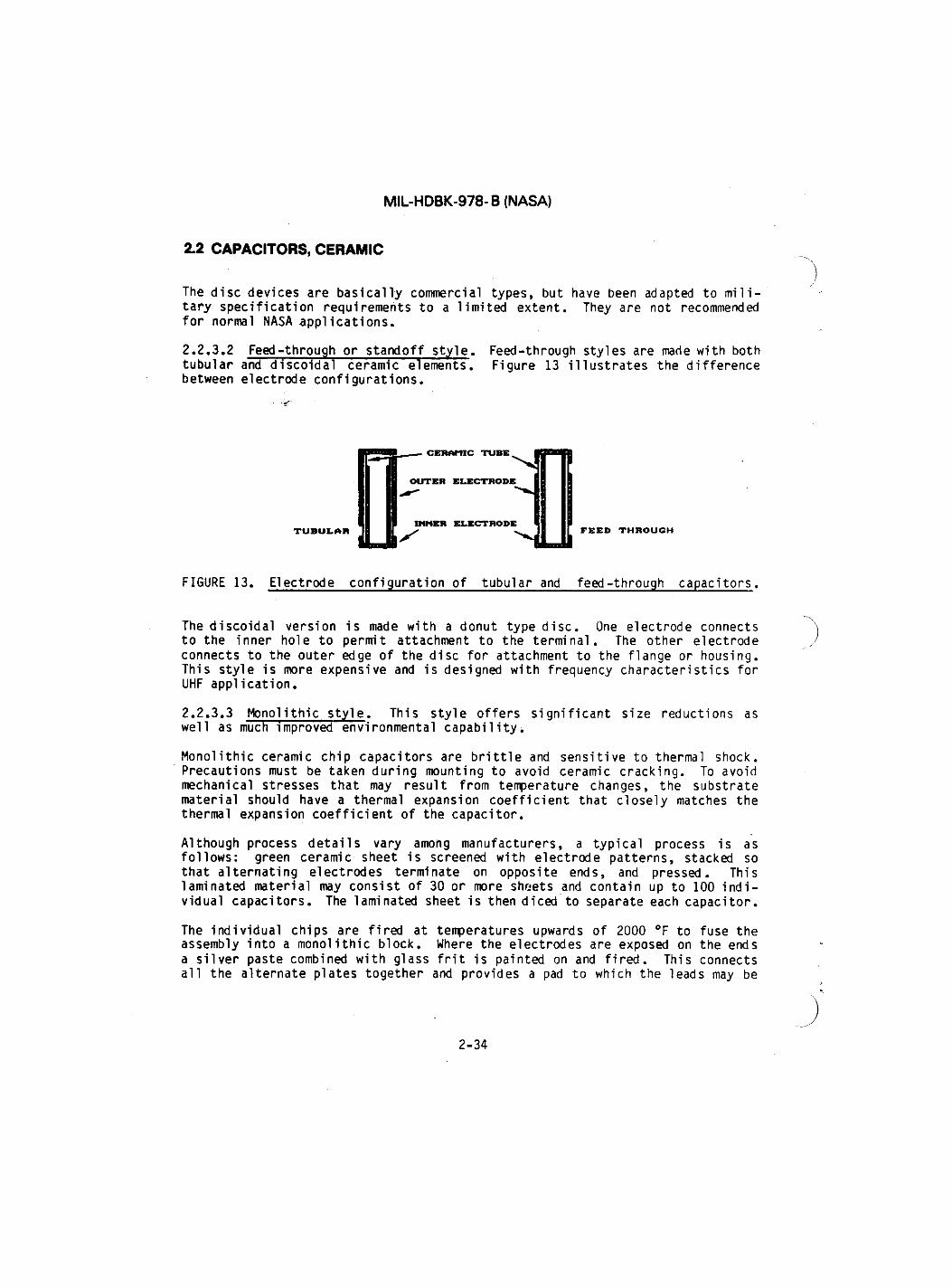
MIL-HDBK-978- B (NASA)
2.2 CAPACITORS, CERAMIC
The disc devices are basically commercial types, but have been adapted to mili-tary specification requirements to a limited extent. They are not recommended for normal NASA applications.
2.2.3.2 Feed-through or standoff style. Feed-through styles are made with both tubular and discoidal ceramic elements. Figure 13 illustrates the difference between electrode configurations.
FIGURE 13. Electrode configuration of tubular and feed-through capacitors.
The discoidal version is made with a donut type disc. One electrode connects to the inner hole to permit attachment to the terminal. The other electrode connects to the outer edge of the disc for attachment to the flange or housing. This style is more expensive and is designed with frequency characteristics for UHF application.
2.2.3.3 Monolithic style. This style offers significant size reductions as well as much improved environmental capability.
Monolithic ceramic chip capacitors are brittle and sensitive to thermal shock. Precautions must be taken during mounting to avoid ceramic cracking. To avoid mechanical stresses that may result from temperature changes, the substrate material should have a thermal expansion coefficient that closely matches the thermal expansion coefficient of the capacitor.
Although process details vary among manufacturers, a typical process is as follows: green ceramic sheet is screened with electrode patterns, stacked so that alternating electrodes terminate on opposite ends, and pressed. This laminated material may consist of 30 or more sheets and contain up to 100 indi-vidual capacitors. The laminated sheet is then diced to separate each capacitor.
The individual chips are fired at temperatures upwards of 2000 °F to fuse the assembly into a monolithic block. Where the electrodes are exposed on the ends a silver paste combined with glass frit is painted on and fired. This connects all the alternate plates together and provides a pad to which the leads may be
2-34

MIL-HDBK-978- B (NASA)
2.2 CAPACITORS, CERAMIC
soldered. The chips are now functional capacitors which are essentially imper-vious to most environmental conditions (Figure 14). Final operations consist of lead attachment and encapsulation (Figure 15).
CERAMIC LAYER
TERM-INATE EDGE
ELECTRODE END TERMINATIONS
ELECTRODES
TERMINATE EDGE M A R G I N
FIGURE 14. Typical construction of a monolithic capacitor chip.
FIGURE 15. Outline drawing of a radial leaded ceramic capacitor (CKR05 Style).
2.2.3.4 Tubular style. The tubular configuration is still used (particularly in the temperature compensating devices), but is rapidly becoming obsolete for military use. The tubular capacitor is fabricated from a tube of ceramic with one electrode painted on the inner surface and terminated at one end of the tube, and the other electrode painted on the outer surface and terminated at the opposite end. Silver bonded with glass frit is the most common electrode material, although others are also used. Its capacitance is limited to low values because of the configuration, and cannot approach the volumetric effi-ciency of monolithic styles.
2-35

MIL-HDBK-978- B (NASA)
2.2 CAPACITORS, CERAMIC
The term "tubular" used here applies specifically to the type of construction described above, and not to the general category of axial-leaded styles in a cylindrical configuration such as the CKR12 and similar styles. These have monolithic capacitor elements and only the external configuration is tubular in shape.
2.2.4 Military designation.
2.2.4.1 Applicable mi 1itary specifications. Ceramic capacitors are covered by the following specifications:
MIL-C-20
MI L-C-123
MIL-C-39014
MIL-C-55681
Capacitors, Fixed, Ceramic Dielectric (Temperature Compensating) Covers CC and CCR Styles.
Capacitors, Fixed, Ceramic Dielectric, (Temperature Stable-BP and General Purpose - BX) High Reliability - covers CKS Style. This is designed for space programs and is an upgrade of MIL-C-55681 and MIL-C-39014. However, it does not cover all values and styles called out in MIL-C-55681.
Capacitors, Fixed, Ceramic Dielectric (General Pur-pose) - Established Reliability - covers CKR styles.
Capacitors, Fixed, Ceramic Dielectric, Established Reliability - covers CDR Style.
2.2.4.2 Part designation. Parts are currently selected by specifying part numbers detailed in the appropriate Mi 1itary Specification slash sheet. For example, the part numbers listed herein describe failure rate level, voltage rating, capacitive value, tolerance, characteristic, style, and other features.
MIL-C-20
CCR75
Style
CH
I Characteristic
IF (0
Capaci tance Capaci tance tolerance
S T
Failure rate
MIL-C-123
M123
Mi 1itary specifi-cation number
Modifi-cation number
01
x Slash sheet
BX 103
T Charac- Voltage Capaci teristic tance
val ue
Capaci -tance tolerance
Termina-tion
2-36

MIL-HDBK-978- B (NASA)
2.2 CAPACITORS, CERAMIC
MIL-C-39014/05-2237
The numbers following the slash describe failure rate, level, voltage rating, capacitance value, and tolerance.
MIL-C-55681
CDR01 BX
Style Rated temper-ature and voltage-temperature limits
1( 30
Capaci tance Rated voltage
K T
Capaci-tance tolerance
S T
Termination finish
Fail ure rate level
Many styles are available in the specifications listed, each with separate capa-citance ranges and voltage ratings. For selection, consult MIL-STD-975 (NASA).
2.2.4.3 Space application. MIL-C-123 was developed for space applications in order to meet the severe environmental conditions encountered in space. MIL-C-123 is a replacement for MIL-C-55681 and MIL-C-39014. MIL-C-123 is designed to include stringent testing requirements such as:
a. One quality level
b. Pretermination Destructive Physical Analysis (DPA)
c. Pre-encapsulation terminal strength
d. Humidity, steady state low voltage criteria
e. Tighter moisture resistance requirements
f. DPA inspection (finished product)
g. 100% inspection for thermal shock, voltage conditioning dielectric withstanding voltage and other electrical parameters.
2.2.5 Electrical characteristics. Because of the wide difference in charac-teristics, capacitance ranges, and applications of Class I and Class II dielec-trics, refer to MIL-STD-975 (NASA) and the individual military specification for the requirements. See Table VIII.
2-37

MIL-HDBK-978- B (NASA)
2.2 CAPACITORS, CERAMIC
TABLE VIII. Electrical characteristics of ceramic capacitors
Characteristic Ceramic Capacitor
NPO BX
Capacitance range (pf) 10 to 68,000 12.0 to 1,000,000
Tolerances 0.1 pf to ±10% ±0.5 pf to ±20%
Voltage rating (Vdc) 50 50 to 1600
Aging (percent/decade) None 1 to 2
Curie point (°C) Outside the range of interest
115
Temperature coefficient 30 ppm/°C +15 to -25 percent
Insulation resistance (Megohm-uf)
1,000 minimum 1,000 minimum
Operating temperature (°C) -55 to +125 -55 to +125
NOTE:
Deaging: The aging process can normally be reversed by exposure to 125°C. Com-plete deaging will occur at 150°C. Both the capacitance and dissipation factor will revert to the former 10-hour levels and then the aging process will resume.
2.2.5.1 Derating. The failure rate of ceramic capacitors under operating con-ditions is a function of time, temperature, and voltage. Refer to MIL-STD-975 (NASA) for specific derating conditions.
2.2.5.2 End-of-life design limits. For general purpose ceramics, the capaci-tance change is ±30 percent and insulation resistance change is -50 percent. Capacitance change for temperature compensated ceramics is ±0.5 percent or 0.45 pF (whichever is greater), and the insulation resistance change is -50 percent.
2-38
MIL-HDBK-978- B (NASA)
2.2 CAPACITORS, CERAMIC
2.2.5.3 Design precautions. BX and BR dielectric ceramic capacitors are rated for dc use and may be used with ac if the sum of the dc voltage and ac peak-to-peak voltage does not exceed the dc rating, and the heat generated does not cause a temperature rise in excess of 35°C. Power can be calculated with the following formula: Watts = E^ (2nfc) (Dissipation Factor). Nominal ratings are 1/8 watt.
Dielectric absorption occurs in all solid-dielectric capacitors and is a significant parameter in pulse and other circuits where rapid charge-and-discharge characteristics are important. In such applications, time delays caused by dielectric absorption may be detrimental to circuit performance. The ratio of the recovery voltage of a capacitor to the initial-charge voltage, expressed as a percentage, is called the percent dielectric absorption. The percent dielectric absorption for a BX dielectric is 2.5 and for BR dielectric is 4.5, and for an NPO is 0.75.
BX and BR dielectric ceramic capacitors exhibit a piezoelectric response when subjected to vibration. Values up to several millivolts can be expected, therefore circuits with a high gain following a capacitor may be sensitive to this effect.
Capacitors, fixed, ceramic, (CCR, CKR, and CDR). Fixed ceramic capacitors (i.e., CCR, CKR, and CDR styles) should meet the destructive physical analysis criteria defined in Table IX, Group A Inspection, of MIL-C-123, and the humid-ity, steady-state, low voltage criteria (+85°C/ 85% RH) defined in Table X, Group B Inspection of MIL-C-123 (100% in order to minimize the risk of low IR failures).
2.2.5.4 Measurement conditions. The capacitance of Class II dielectrics is affected by variations in voltage and frequency, particularly as the dielectric becomes thinner as in the case of monolithic styles. Therefore, measurement voltage must be specified; e.g. MIL-C-123 specifies 1.0 Vrms @ 1,000 Hz as a measurement potential. This is used as a standard for all measurements on parts having a 50 Vdc rating or greater.
Class I dielectric capacitance is largely independent of voltage and frequency within the ratings of the device. However, standard measurement conditions similar to those of Class II dielectrics are normally specified.
2.2.5.5 Dissipation factor or "Q". For Class II dielectrics, the dissipation factor will seldomly affect circuit operation except in specific applications requiring the high Q of the Class I dielectrics. Class II dissipation factors range between 1.0 and 4.0 percent, although military grades are normally no higher than 2.5 percent. The primary purpose for checking this parameter is that for a given dielectric, variation in dissipation factor may provide the manufacturer with information on formulation and firing variations. An excep-tionally high dissipation factor indicates poor termination (cold solder joint, lifted electrode, separated lead, etc.).
2-39

MIL-HDBK-978- B (NASA)
2.2 CAPACITORS, CERAMIC
Often differences in dissipation factor as slight as 1.5 percent vs 2.0 percent are exploited as sales gimmicks. Figure 16 shows the effects of temperature-vs-dissipation factor. The dissipation factor at -55°C increases by 5 to 10 percent depending on formulation. In this case, the dissipation factor of the bismuth-free body, although slightly higher at room temperature, is signifi-cantly lower at -55°C.
, BL! \ K
SMUT 1200
H BODY
NON B ISMUTH K 1800
-55 -25 O 25 50 75 100 125 T E M P E R A T U R E D E G R E E S CENT IGRADE
FIGURE 16. Dissipation factor vs temperature.
The dissipation factor is affected by measurement voltage and frequency; since this measurement is normally made at the same time as capacitance, the same comments apply.
The Class I dielectric dissipation factor for these devices is less than 0.1%. This parameter is sometimes expressed as Q, which for capacitors is the recipro-cal of the dissipation factor expressed as a pure number. A dissipation factor of 0.1% corresponds to a Q of 1000.
2.2.5.6 DC voltage coefficient. Class II ceramic capacitors have a voltage coefficient that normally becomes greater as dielectric constant increases. This effect is dependent on the formulation as well as dielectric thickness. Figure 17 illustrates the effect of dc voltage on K1800 material. Note that this effect is not linear; although there is a change of 10 percent at rated voltage, the change at 50 percent of rated value is only about three percent, while below 30 percent of rated voltage the change is either negligible or slightly positive.
2-40

MIL-HDBK-978- B (NASA)
2.2 CAPACITORS, CERAMIC
PERCENT RATED VOLTS
FIGURE 17. Capacitance change vs dc voltage.
The curves in Figure 18 show the combined effect of voltage and temperature. Voltage coefficient is greater at low temperatures than at high temperatures and therefore -55°C is usually the point of greatest change for a given characteristic.
Class I dielectric curves are not shown for voltage coefficient, since these dielectrics are not particularly sensitive to voltage. Depending on the formu-lation, the voltage coefficient varies from negligible to a maximum of about 2%.
UJ O z
O 2 lug 5 w
n < Q. < O
15 10 5 0 5
10 15 20 25 30 35 40
4 T * / r 4 / * /
/ / f /
f /
. — 50« R0 VOLTS APPLIED 16 RATED VOLTS APPLIED -)% RATED VOLTS APPLIED..
i l l
. — 50« R0 VOLTS APPLIED 16 RATED VOLTS APPLIED -)% RATED VOLTS APPLIED..
i l l 1 1
R0 VOLTS APPLIED 16 RATED VOLTS APPLIED -)% RATED VOLTS APPLIED..
i l l -50 -25 0 25 50 75 100 TEMPERATURE IN DEGREES CENTIGRADE
125
FIGURE 18. Typical combined effect of voltage and temperature,
2-41
MIL-HDBK-978- B (NASA)
2.2 CAPACITORS, CERAMIC
2.2.5.7 AC voltage effects. For Class II dielectrics, the effects of ac voltage on capacitance and dissipation factor are also dependent on material and volts per mil stress. It is this latter effect that makes measurement voltage more critical as the dielectric decreases in thickness. A capacitor with a 1 mil dielectric thickness is much more sensitive to 2.0 Vrms than a 20-mil-thick disc.
Figure 19 shows the effects of ac voltage on the capacitance of typical capaci-tors. Note that, an increase in ac voltage causes an increase in capacitance, opposite to the effects of dc voltage.
Dissipation factor also increases with ac voltage. For example, dissipation factor measured at 1.0 Vrms for K1800 dielectric is about 3% and increases to about 8% at a measurement voltage of 3.0 Vrms, 1 kHz.
S 50 ac UJ
o z
S 20 Z < fc 10 (J <
FIGURE 19. Capacitance vs ac voltage.
Class I dielectrics maintain their capacitance and dissipation factor charac-teristics when used within their voltage ratings.
2.2.5.8 Temperature characteristies. Figure 20 shows typical temperature characteristics of Class TI ceramic dielectrics. It can be seen that the temperature stability of the capacitor decreases with increasing dielectric constant.
/ < 1 800
KJ >50
12.5 25 37.5 50 VOLTS AC AT 1.0 KHz
2-42

MIL-HDBK-978- B (NASA)
2.2 CAPACITORS, CERAMIC
H 15 2 UJ O cc 10 UJ
. a. UJ a 5 z < i 0 o UJ o z -5 < K 5 -10 < -10 a <
-15 u -15
K 250 ^
J R
f K U 300
-55 -25 0 25 50 75 100 125 TEMPERATURE DEGREES CENTIGRADE
FIGURE 20, Capacitance change vs temperature,
Higher dielectric constant materials are available, but with decreasing stability and a narrower operating range of -55°C to +85°C. For example a K5600 dielectric would give 4 times the capacitance of K1800 dielectric at 25°C, but could lose 60 percent of its capacity over the temperature range. A K8000 dielectric would give 6 times the capacitance but lose 80 percent of its capacity. These dielectrics are effective only in controlled ambient con-ditions where full use may be made of the increased capacitance at 25°C without concern for the falloff at temperature extremes.
The most distinguishing feature of the Class I ceramics is their relatively linear change in capacitance with temperature. This change will vary depending on-formulation from P100 (positive 100 ppm/°C) to N5600 (negative 5600 ppm/°C). The Class I dielectrics are identified by their nominal temperature coefficient (TC). It is important to remember that this TC is determined from a two point measurement of capacitance at 25°C and at 85°C. These materials have a more negative TC as the temperature approaches -55°C. This is covered by specific TC limits over the temperature range. Additionally, there is a tolerance on the nominal TC which varies from ±30 ppm for NPO to ±1,000 ppm for N5600. Effec-tively, an NPO ±30 ppm will have a temperature coefficient falling between a +30 ppm and a -30 ppm limit. Figure 21 shows the temperature characteristic for a N330 ±60 ppm envelope (note that it is more negative on the cold side). Also important is the fact that the tolerance is necessarily greater for low capaci-tance values (less than 10 pF), because stray capacitance becomes a factor and the temperature coefficient of the stray capacitance has an effect.
2-43
MIL-HDBK-978- B (NASA)
2.2 CAPACITORS, CERAMIC
Z UJ o ac UJ OL UJ 0 z < 1 U UJ o z < 5 < Q_ < o
5 4 3 2 1 0 -1 -2 -3
c AP. VS. TEN 330 ± 60 PP
AP. N
AP. VS. TEN 330 ± 60 PP M
N
-55° -25° 0° 25° 50° 75° 100° 125°
TEMPERATURE DEGREES CENTIGRADE
FIGURE 21. Temperature vs capacitance.
2.2.5.9 Effects of frequency. Figures 22 and 23 show comparative effects frequency for three typical formulations. Actual plots vary, depending capacitance value, configuration, and lead length. However, these illustra-tions provide general information in selecting the capacitor type particular application.
of on
for a
It can be seen and that the Q high-K material
that Class I (NPO) dielectrics are least affected by frequency, of the NPO dielectric is several times better than that of the
uu O Z <
S 3 ? X M, UJ t Q-5 < Q. < <J
-10
-20
-30
NPO /
K 1 800 ^ S K 250
CAI I 5ACIT/ ! I
\NCE \ i I
fS FRE I I
:QUEN ! I
CY
1 KHZ 100 KHZ 10 MHZ 1 GHZ 10 KHZ 1 MHZ 100MHZ
FREQUENCY
FIGURE 22. Capacitance vs frequency.
2-44

MIL-HDBK-978-B (NASA)
2.2 CAPACITORS, CERAMIC
2000
1600 £ O £ 1200 <
b 800
400
0
FIGURE 23. "Q" vs frequency.
2.2.5.10 Aging. Class II ceramic capacitors exhibit a characteristic referred to as aging; i.e., a decrease in capacitance with time. Class I dielectrics are not subject to this phenomenon and are quite stable in storage and operation.
During storage at room temperature there is a decrease in the dielectric con-stant due to crystalline structural changes in barium titanate. The magnitude of these changes increases as the dielectric constant increases.
These changes are exponential with time, and aging is normally expressed as percent capacitance change per logarithmic unit of time (such as 2 percent per decade). Time zero in such computations relates to the last exposure to a temperature in excess of 125°C, and time is expressed in hours. Figure 24 shows typical aging curves based on an aging rate of 2.5 percent for K250 dielectric and 4.0 percent for K1800 dielectric material.
Due to its exponential rate, aging on a linear time base is relatively low after 1,000 hours. Manufacturers normally allow for aging when measuring capacitance, so that purchase tolerances will tend to run on the high side of nominal. Longer shelf life can be guaranteed by preaging and sorting to tighter guard bands.
Dissipation factor is also affected by aging, with a gradual decrease occurring during storage. Since this change is favorable and not of great magnitude, it is usually unimportant.
Q VS FREQUENCY
K 250V K 1800
1 KHZ 100 KHZ 10 MHZ 1 GHZ 10 KHZ 1 MHZ 100 MHZ
FREQUENCY
2-45

MIL-HDBK-978-B (NASA)
2.2 CAPACITORS, CERAMIC
FIGURE 24. Aging curves, Class II dielectrics.
Application of a high voltage, (e.g., during a dielectric strength test) will cause a decrease in capacitance. Provision is made for this effect in the applicable specification, which permits a waiting, period for capacitance and power factor to age into tolerance after such exposures.
2.2.5.11 Deaging. The aging process can be reversed by exposure to 125°C with complete deaging usually occurring at 150°C. Both capacitance and dissipation factor will revert to the former 1.0-hour levels and the aging process will resume.
2.2.5.12 Life. Both Class I and Class II ceramic capacitors will normally operate for several thousand hours when properly derated. However, Class II ceramic capacitors will generally demonstrate a decrease in capacitance of 10-15% in a standard thousand-hour life test at maximum conditions. Although this is apparently the result of different phenomena within the crystalline structure, it is similar in effect to shelf aging. Because of the ferroelectric nature of the Class II formulations, these capacitors usually exhibit less change in capacitance when tested at 125°C, as compared to being tested at 85°C, because some deaging takes place at the higher ambient.
Class I ceramic capacitors typically exhibit less than one percent change in a similar life test.
2-46
MIL-HDBK-978-B (NASA)
2.2 CAPACITORS, CERAMIC
2.2.6 Environmental considerations. Barium titanate has a piezoelectric effect and voltage transients may be produced by mechanical stresses such as vibration and shock. This effect is greater on high-K bodies. It occurs after the dielectric has been polarized by the application of voltage at high temper-ature. It is for this reason that voltage conditioned capacitors exhibit a greater piezoelectric effect.
Voltages in the order of 150 microvolts have been measured under some vibration test conditions. Where this effect may be deleterious to satisfactory circuit operation, consideration should be given to using a Class I dielectric or isolating the capacitor from mechanical stress.
2.2.7 Reliability considerations.
2.2.7.1 Failure modes. Ceramic capacitors usually fail because of an open circuit, short circuit, or because of parameter degradation, (low insulation resistance or excessive change in capacitance with temperature).
The most common failure modes are the catastrophic failures, i.e., opens and shorts. Significant parameter degradation failures are relatively rare and in many applications are unnoticed unless the changes are extreme.
2.2.7.2 Failure mechanisms.
a. Shorts. Operation under voltage stress can result in shorts due to puncture through the ceramic. This failure mode is common to all styles of ceramic capacitors and results from contaminants in the dielectric, hairline cracks, thin spots in the dielectric, or voids. These failure mechanisms can be precipitated before installation in the end equipment by proper screening techniques, particularly voltage conditioning.
b. Opens. Opens are the major problem with monolithic ceramic capacitors, particularly the smaller axial-leaded configurations (0.1" diameter and less). These devices employ nailhead or paddle-shaped leads soldered to the end terminations and depend mainly on the epoxy encapsulation for mechanical integrity. Unfortunately, the encapsulation process, which is usually accomplished by transfer molding at high pressures, will fill any voids in the joint between the lead and the ceramic. The epoxy will then tend to open the connection by lifting the lead away from the chip. This failure mechanism is insidious and often occurs only at specific temperatures, or may result in intermittent opens at a given temperature.
c. Low insulation resistance. This may occur as the result of surface contamination during manufacture or because of moisture penetration through a defective epoxy encapsulation. Monolithic ceramic capaci-tors, when properly cured and fired, are impervious to moisture as
2-47

MIL-HDBK-978-B (NASA)
2.2 CAPACITORS, CERAMIC far as the chip is concerned, but the shunt path formed by contaminants or surface moisture may result in circuit failures. Low insulation re-sistance failures may also occur in low-voltage, high-impedance circuit applications. Applying rated voltage will temporarily clear the part. Failures of this nature should be verified by measuring insulation re-sistance at 1.5 Vdc.
d. Processing problems. Contaminants in the dielectric, ha1rline cracks* thin spots* voids, and del ami nations are some of the processing related problems that may cause failure of monolithic multllayered ceramic capacitors. These defects result 1n time, temperature, and environmental related failure mcchanlsms which have been a serious cause of ceramic capacitor failure both at the part and equipment level.
The problem 1s more acute with thinner dielectrics, I.e. higher value capacitors, where voids can reduce effective dielectric thickness to dangerously low levels, and hairline cracks and delamlnations can easily propagate under stress. When exposed to humid conditions ceramic capacitance with dielectric defects can demonstrate failures even at low applied voltages (low voltage failure mode). This mechanism results 1n low Impedance between the plates leading to a short circuit.
Adequate tests and screening can be applied to detect these dielectric problems. Destructive physical analysis 1s sometimes used to detect voiding and delam1nat1on. MIL-C-123 employs both screening and lot acceptance tests to control such defects for high reliability applications.
2.2.7.3 Screening. Temperature cycling, operating voltage conditioning and x-ray are usually performed to screen out manufacturing defects and potential early life failures.
2.2.7.4 Reliability derating. If manufacturing anomalies and early life fail-ures have been eliminated by screening techniques, the failure rate of all ceramic capacitors under operating conditions becomes a function of time, tem-perature, and applied voltage. Operational life can be significantly lengthened by voltage derating and by limiting the maximum operating temperature.
Assuming an empirically established failure rate for a given style of ceramic capacitor, the actual failure rate is approximately proportional to the 3rd power of the ratio of the applied voltage to the test voltage. Thus an average failure rate of 0.20%/1000 hours at maximum rated voltage can be reduced to about 0.025%/1000 hours (an improvement by a factor of 8) by operation at 50% of rated voltage.
The derating guideline for ceramic capacitors are specified in MIL-STD-975 (NASA).
2.2.7.5 Failure rate determination. Because of the wide variety of styles and voltage ratings available in ceramic capacitors, and rapid changes in tech-nology, the latest issue of MIL-HBK-217 should be consulted for quantitative failure rate determination.
2-48

MIL-HDBK-978-B (NASA)
2.4 CAPACITORS, PAPER AND PLASTIC
2.3 Mica and glass.
2.3.1 Introduction.
2.3.1.1 Mica. Mica is one of a very few natural materials directly adaptable for use as a capacitor dielectric. Its physical and electrical properties, and its rare tendency to nearly perfect cleavage make it probably the best natural capacitor dielectric known. It is inherently stable, both dimensionally and electrically, so that mica capacitors exhibit excellent temperature coefficient characteristics and very low aging with operation.
The property of perfect cleavage enables blocks of mica to be split into sheets as thin as 0.0001 inch. The surfaces of the split sheets are parallel along the planes of natural crystalline structure.
Most capacitors are made from muscovite mica, which is the best of several natural varieties. It has a dielectric constant between 6.5 and 8.5, and is capable of operation at temperatures up to 200°C.
2.3.1.2 Glass. Glass dielectric capacitors were developed mainly as a sub-stitute for mica. Their electrical characteristics are very similar to those of mica capacitors. They have excellent long-term stability, a low temperature coefficient, and a history of good reliability.
2.3.2 Usual applications. Both glass and mica capacitors are designed for use in circuits requiring relatively low capacitance values, high Q, and good stability with respect to temperature, frequency, and aging. They may be used for high-frequency coupling and bypassing, or as fixed elements in tuned cir-cuits. Their inherent characteristics of high insulation resistance, low power factor, low inductance, and excellent stability make them particularly well suited for high frequency applications.
Although glass and mica styles are essentially interchangeable from an electri-cal standpoint, first consideration should be given to the mica units because of the difference in cost.
Glass dielectric types cost 2 to 10 times as much as an equivalent mica type, depending on capacitance value, tolerance, and quantity.
2.3.3 Physical construction. The commonly used mica styles have either a molded case or dipped construction, such as the CMR04, CMR05, and CMR06. In either case, the capacitor consists of a stack of mica sheets onto which a thin layer of silver is screened and fired. Thin slips of conducting foil are inserted at alternate ends to provide a conducting path to the silvered plates, folded over at the top of the stack, and clinched together with a clamp-lead assembly. The axial leaded styles are then molded in a polyester plastic case. The more popular radial leaded styles are dipped several times
2-49

MIL-HDBK-978-B (NASA)
2.4 CAPACITORS, PAPER AND PLASTIC
in an electrical grade phenolic resin, followed by a final vacuum impregnation with epoxy resin. This results in a physically rugged assembly with high moisture resistance and excellent electrical properties (see Figure 25).
V
FIGURE 25. Outline drawing of a radial leaded mica capacitor (CMR05 style).
Glass capacitors are made by stacking alternate layers of aluminum foil and glass ribbon until the desired capacitance is obtained, then fusing the assembly into a monolithic block as shown in Figure 26. The same glass composition is used for both the case and the dielectric, insuring that the electrical proper-ties of the capacitor are entirely those of the dielectric material. Leads are welded to the electrodes, and a glass-to-metal seal is formed at the entrance to the case. There is some question as to whether a true hermetic seal is formed, but the capacitors are highly resistant to environmental moisture.
GLASS COVER GLASS DIELECTRIC ALUMINUM FOIL
LEAD-FOIL WELD AREA
A C T I V E ELEMENT
GLASS-TO-METAL SEAL
FIGURE 26. Typical construction of the glass-dielectric capacitor,
2-50
MIL-HDBK-978-B (NASA)
2.4 CAPACITORS, PAPER AND PLASTIC
2.3.3.1 Feed through and stand-off configurations. Mica capacitors are also made in "button" style for RF bypassing and feed through applications. These are available in the CB series of styles in accordance with MIL-C-10950. The hermetically sealed styles such as the CB60 series are preferred over the non-hermetic resin-sealed styles such as the CB11 series. They are high-quality units intended for use at frequencies up to 500 MHz.
These capacitors are composed of a stack of silvered-mica sheets connected in parallel. This assembly is encased in a metal shell with a high potential terminal connected through the center of the stack. The other terminal is formed by the metal shell connected at all points around the outer edge of the electrodes. This design permits the current to fan out in a 360-degree pattern from the outer terminal, providing the shortest RF current path between the center terminal and chassis. The internal construction results in minimum external inductance associated with the capacitor. The units are then welded and hermetically glass sealed.
2.3.4 Military designation.
2.3.4.1 Applicable military documents. Mica and glass capacitors are covered by the following military specifications:
MIL-C-10950 Capacitors, Fixed, Mica Dielectric, Button Style CB, (covers feedthrough and stand - off styles, hermetically sealed and resin sealed.)
MIL-C-23269
MIL-C-39001
Capacitors, Fixed, Glass Dielectric, Established Reliability, (covers glass dielectric styles CRY).
Capacitors, Fixed, Mica Dielectric, Established Reliability, General Specification For (covers radial lead dipped styles CMR).
2.3.4.2 Part designation. The type designation for mica capacitors per MIL-C-39001 is shown below. Although similar for other types of mica and glass capaci-tors, the applicable specification should be consulted for other types.
CMR05
Style
C |
Character-istic
100 D
Capacitance
T | T 1
Capacitance Temperature Rated Fail ure tolerance range voltage rate
level
2.3.5 Electrical characteristies.
2.3.5.1 Derating. The failure rate of mica and glass capacitors under operat-ing conditions is a function of time, temperature, and voltage. Refer to MIL-STD-975 (NASA) for specific derating conditions.
2-51

MIL-HDBK-978-B (NASA)
2.4 CAPACITORS, PAPER AND PLASTIC
2.3.5.2 End-of-life design limits. Capacitance change for mica capacitors is ±0.5 percent and for glass dielectric it is +0.5 percent or 0.5 pF (whichever is greater). The insulation Resistance change for mica is -30 percent and for glass it is 500,000 megohms at +25°C and 10,000 megohms at +125 °C.
2.3.5.3 Voltage rating. Glass and mica dielectric capacitors are available as standard parts in the following voltage ranges:
Dipped mica style: 50 to 500 V Button mica style: 500 V Molded mica style: 300 to 2500 V Glass style: 100, 300, and 500 V
These are generally operable over the temperature range of -55°C to +125°C at full rated voltage.
2.3.5.4 Capacitance and tolerance. Glass capacitors are available in capaci-tance values from 0.5 to about 10,000 pF in the commonly used styles, and up to 150,000 pF in the larger transmitting types. Tolerances down to ±1% or 0.25 pF, whichever is larger, are standard.
The same general range is covered by the dipped and molded mica styles of MIL-C-5 and MIL-C-39001, except that minimum available value is 1.0 pF, and the maximum value is somewhat higher. Dipped micas are made up to about 50,000 pF, but are not widely used in the higher values because of their size. The most popular range for both glass and mica capacitors is 1000 pF and less.
Button mica styles are available up to 2400 pF, in tolerances of ±1, ±2, 5, or 10%.
2.3.5.5 Dissipation factor or "Q." Capacitor losses, expressed as DF (dissipa-tion factor) or Q, which is equal to 1/DF, are a function of the measurement frequency. Maximum dissipation factors for mica and glass capacitors procured to MIL-C-23269 and MIL-C-39001 are shown in Figure 27. DF is measured at 1 MHz for values equal to 1000 pF or less, and at 1 KHz for values above 1000 pF.
Glass capacitors demonstrate somewhat lower losses, particularly in the small capacitance values. This is because tighter controls can be maintained on the composition of the glass and less allowance must to be made for material varia-tions. Also, the internal terminations are welded, rather than clinched, allow-ing for greater uniformity.
A simpler evaluated comparison for many applications is shown in Figure 28, which depicts comparative Q at 1 MHz. In the midranges of capacitance, both glass and mica are comparable, but glass is superior at both the high and low ends of the capacitance range. Further comparisons are discussed in paragraph 2.3.5.7 on effects of frequency.
2.3.5.6 AC voltage ratings. Glass capacitors of the CYR series may be operated with an impressed ac voltage provided that the peak value of the applied voltage
2-52

MIL-HDBK-978-B (NASA)
2.3 CAPACITORS, MICA AND GLASS
does not exceed the maximum rated dc voltage. This rating applies for power line frequencies and through the audio frequency range. For operation at high frequencies, the power dissipated in the capacitor becomes the limiting factor.
CE .01 o »-o < IL 2 O
O .001
.0001
M A X I M U M DISSIP. FOR CAPACITANC
AT ION F A C T O R A T 1 :E V A L U E S OF IOOOP
MHZ f OR LESS
M|CA
M I C A >
GLASS
/
M A X I M U M DISSIP/ 1 KHZ FOR CAPAC G R E A T E R T H A N 1
\
kTION F A C T O R AT ITANCE V A L U E S 000 pF
1 ! I ! II
\ f Mill 1 1 1 1II I M M I I I I I
10 100 1.000 CAPACITANCE IN pF
10,000 100,000
FIGURE 27. Dissipation factor vs capacitance.
10,000 p
a i.ooo
100
I
III II
I I
1
GLASS
\
)
MICA
i I
III II
I I
1
GLASS
\ /
1 1 1 I I I I I i > i i n t i 1 1 1 1 M i l 1 1 1 1 1 1 1 1 1 1 1 1 1 M l 10 100
C A P A C I T A N C E (PF) 1,000 10,000
FIGURE 28. Q vs capacitance at 1 MHz.
2-53

MIL-HDBK-978-B (NASA)
2.4 CAPACITORS, PAPER AND PLASTIC
Mica capacitors can be operated under ac conditions, but the generally higher dissipation factor, as well as the possibility of corona initiation at relative-ly low ac voltages must be considered. Each potential ac application of mica capacitors should be reviewed for part capability before the design is fixed. Mica capacitors are more susceptible to corona problems at high ac voltages because of the presence of microscopic voids which may contain air.
2.3.5.7 Effects of frequency. Since these types of capacitors are often used in circuits where the designer is concerned with high frequency performance, the following should be considered: capacitance variation with frequency, self-resonant frequency, Q vs frequency, and RF current capability.
Capacitance vs frequency. Mica capacitors remain quite stable with frequency from low audio through radio frequencies. Capacitance variation in this ranye is measured in hundredths of a percent. In the VHF range (30 MHz and up) the apparent capacitance tends to gradually increase and may show variations as high as 10% above the 1 MHz measurement as frequency is raised still further. This variation of capacitance with frequency becomes more pronounced as the capacitance value increases, v
Glass capacitors are also stable with frequency, as shown in Figure 29. In this case, apparent capacitance tends to gradually decrease with increasing frequency.
< -1-5 z " +4
L +2 1*1 S 0
UJ o fiL
-4 -5
FIGURE 29. Typical capacitance change vs frequency for glass dielectric capacitors.
Self-resonant frequency (SRF). An upper limit of usual operating frequency range is established by the self-resonant frequency of a capacitor. For both mica and glass styles the length of the leads is a significant factor in the SRF. For a given case size, the inductance of the leads and internal termin-ations is approximately constant, so that the resonant frequency is approxi-mately inversely proportional to the square root of the capacitance.
— •
1 1 1 Hill i iiinn i i nun i i linn I I IIIIII 1 KHz lOKHz lOOKHz 1MHz
FREQUENCY
2-54

MIL-HDBK-978-B (NASA)
2.4 CAPACITORS, PAPER AND PLASTIC
Figures 30, 31, and 32 show typical curves for glass and dipped mica styles.
FIGURE 30. Typical curves of self resonant frequency vs capacitance for types CYR10, CYR15, CYR20, and CYR30 glass dielectric capacitorsT
-
•
1 1 1 11 I I I 1 1 1 1 l l l l I 1 I I l l l l
LEAO LEIS
1 1
IGTH IN INCHES
j Mint 10 100 1000 10.000 CAPACITANCE IN pF
FIGURE 31. Resonant frequency of a typical dipped mica capacitor (type CMR05).
2-55

MIL-HDBK-978-B (NASA)
2.4 CAPACITORS, PAPER AND PLASTIC 1
1 1
1 I 1
II / /H
N
v s s .
I I II 1111
L E A D L E N
Va —
I I 1 M III!
G T H IN INCHES
1 * 1 1 1 1 1
VS. v s s . O n S .
v x \
1 1 II 1 111 10 100 1000 10,000 100,000
C A P A C I T A N C E IN pF
FIGURE 32. Resonant frequency of a typical dipped mica capacitor (type CMR07).
Q vs frequency. Figures 33 and 34 show typical curves of Q and DF as a func-tion of frequency. Glass capacitors are superior to mica in this respect, particularly at frequencies in the range of 1 MHz and above.
RF current capacity. Except for large transmitter type capacitors, little information is available concerning RF current-carrying capability of glass and mica capacitors. Such information is often required, since these units are used in high frequency applications. However, the practically infinite variety of voltage, frequency, and case size combinations makes compilation of compre-hensive data a formidable task. The following information can be used as a guideline for such applications (Figure 35).
2-56

MIL-HDBK-978-B (NASA)
2.4 CAPACITORS, PAPER AND PLASTIC
10,000
10KHz TOOK Hz 1MHz FREQUENCY
10MHz 100MHz
FIGURE 33. Q and DF vs frequency for typical glass capacitor
3500
3000
2500
2000
1500
1000
500
0
\ \ i\ \\
\ \ \ \
C « E >0pF C x / 25pF
c = 3 90pF-4
X « 11 1 00 pF C * 2!
J 50pr-i X « 11 1 00 pF
5 10 15 20 25 30 35 40 F R E Q U E N C Y IN MEGAHERTZ
FIGURE 34. Q vs frequency for typical dipped mica capacitor (type CMR05, 500 VDCK
2-57

MIL-HDBK-978-B (NASA)
2.4 CAPACITORS, PAPER AND PLASTIC
4.0
3.0
a. 5 < CO 5 a:
z Ui QC QC D CJ
2.0
1.0
FREQUENC I Y 1.0 MHz
CM WO 7 -! 500 W.V.
2000 4000 6000 C A P A C I T A N C E (pF)
8000 10,000
2.0
CO Q. < 00 5 QC
H Z UJ QC QC D O
1.0
FRI I EQUENCY 3.0 P
I tfHz
C A P A C I T A N C E (pF)
FIGURE 35. Radio frequency current ratings for dipped mica capacitors.
2-58
MIL-HDBK-978-B (NASA)
2.4 CAPACITORS, PAPER AND PLASTIC
Glass capacitors (CYR10, CYR15, CYR20). The following maximum volt-ampere ratings are acceptable limits for these capacitors:
CYR10 - 400 VA CYR15 - 600 VA CYR20 - 1100 VA
These ratings are based on a case temperature rise of 45°C which limits the operating ambient temperature to 70°C. For operation at higher ambients, the dissipation must be reduced to limit the maximum case temperature to 125°C. In any case, the peak value of the ac voltage plus dc bias must not exceed the dc rated voltage of the capacitor.
Dipped mica capacitors. The curves shown in Figure 35 represent typical manufacturers1 recommendations for safe limits of RF current for dipped mica units of various case sizes. These curves are based on a case temperature rise of 15°C. This lower temperature rise limit is imposed because of the greater tendency of mica units to develop hot spots due to corona breakdown or dielectric imperfections, as compared to the more nearly homogeneous glass devices. Again, the peak amplitude of the combined ac and dc applied voltages must not exceed the dc voltage ratings, and the temperature rise plus ambient temperature must not exceed the maximum operating temperature rating of the capacitor.
2.3.5.8 Effects of temperature. As stated previously, one of the significant advantages of glass and mica capacitors is their stability with temperature.
Glass has a fairly uniform positive temperature coefficient of capacitance. As measured at 100 kHz, the TC is equal to 140 ±25 PPM/°C. This translates into a capacitance change (from the 25°C value) of approximately +1.5% at 125°C, and -1.0% at -55°C.
2.3.6 Environmental considerations. Both glass and mica devices, as procured to the appropriate specification, are adequate for most environments, including exposure to extreme humidity and high levels of shock and vibration.
For severe vibration environments, the cases of the radial-leaded dipped mica styles in particular must be adequately anchored to prevent failure due to lead fatigue.
2.3.7 Reliability considerations. Both glass and mica dielectric capacitors when used well within their voltage and temperature ratings* will operate reliably for several thousand hours. However since construction methods vary with different vendors, physical differences should be examined and analyzed for use 1n the Intended application.
2-59

MIL-HDBK-978-B (NASA)
2.4 CAPACITORS, PAPER AND PLASTIC
2.3.7.1 Failure modes and mechanisms. The most common failure mode for these capacitors is eventual short circuit due to dielectric breakdown. Failure rate varies directly with capacitance value for a given case size, simply because of the increase in the number of plates as capacitance increases. The failure rate of micas would be expected to be higher than glass, because of the greater opportunity for flaws in the natural dielectric, but historical data does not indicate this. The development of the dipped mica style represented an improve-ment over the molded types because of the elimination of the high heat and pressures of molding. These stresses tend to weaken or fatigue the mica films sufficiently to make the effect noticeable in long-term life tests.
A broadly experienced failure mode exhibited by mica capacitors is caused by poor mechanical clamping of the lead end clips to the capacitor foil stack. This mechanical connection, if not processed properly, is prone to develop electrical intermittants over temperature excursions. Because of this, mica capacitors are not listed in MIL-STD-975. Use of these should be avoided for critical applications. If it is absolutely necessary to use these capacitors, a 100% monitored temperature cycling test should be performed to detect and remove any intermittant devices.
2.3.7.2 Screening. Early life failures are best screened out by a condition-ing period -oT^u hours or more under over-voltage stress. Glass capacitors are typically conditioned at 300% of rated voltage at 25°C, and micas at 200% of rated voltage at 150°C. These conditions reflect variations in manufac-turers1 standard approaches to screening, rather than any basic difference in part susceptibility to failure. Temperature cycling is also often specified prior to conditioning, in order to assist in precipitation of failure of parts with mechanical weakness or poor internal connections.
To screen out early life failures, the following screening tests are usually performed: temperature cycling, operating burn-in or high voltage stabiliza-tion, and X-ray.
2.3.7.3 Failure rate. Figures 36 and 37 depict typical curves of capacitor failure rate as a function of voltage and temperature stress. These curves represent an accumulation of data including field experience and controlled laboratory tests. They do not represent screened or established reliability parts. For quantitative reliability predictions, current failure rate data should be consulted. These curves, however, can be used to provide an order-of-magnitude estimate as to probable performance. For further information refer to MIL-HDBK-217.
2-60

MIL-HDBK-978-B (NASA)
2.4 CAPACITORS, PAPER AND PLASTIC
FIGURE 36. Failure rates (in failures per 106 hours) for MIL-C-11Z7Z, glass and porcelain capacitorsT"
2-61

MIL-HDBK-978-B (NASA)
2.4 CAPACITORS, PAPER AND PLASTIC
OPERATING RATED
.1 .08
CO .06 X .06
D O X .04 z O ZJ -I 5 0.02 X Ui Q. c/5 UJ .01 <E D
.008 mJ < .006
UJ .004 K < X UJ X .002 D -j < u.
.0004 -
.0002
.0001 40 60 80 100
PART AMBIENT TEMPERATURE (©C)
V O L T A G E RATIO
120 140
FIGURE 37. Failure rates (in failures per 106 hours) for MIL-C-5, dipped mica capacitors, temperature range 0-125°C, characteristic 0.
2-62

MIL-HDBK-978-B (NASA)
2.4 CAPACITORS, PAPER AND PLASTIC
2.4 Paper and plastic.
2.4.1 Introduction. Paper, plastic, and paper-plastic dielectric capacitors serve the broad middle ground of capacitor requirements. This group includes a wide variety of dielectric systems, styles, voltage ratings and temperature characteristics useful in applications once restricted mainly to wound paper-foil devices. Although the remarks in this section apply mainly to the common tubular configuration, these capacitors are available in a great variety of combinations of case styles and electrical ratings for particular applications.
Some of the more commonly used types are: paper-foil, metallized paper, Mylar-foil, metallized Mylar, metallized paper-Mylar, polystyrene-foi1, Teflon-foil, polycarbonate-foil, and metallized polycarbonate.
2.4.2 Usual applications. These capacitors are used in most types of applica-tions, including coupling, bypassing, filtering, timing, noise suppression, and power factor correction. They are useful over frequency ranges up to 10 MHz or more, depending on capacitance value and type of construction. They have high insulation resistance, fairly good stability, and can operate at ambient temperatures up to 125°C and above. Certain types of plastic dielectric such as polycarbonate, polystyrene, and Teflon also have excellent temperature coefficient characteristics.
Any ac-rated capacitor can be used in an equivalent dc circuit. However, the converse is not true because of dielectric heating, corona, and resistance heating (Rs).
For high frequency ac applications, the dissipation factor (DF) of each capaci-tor should be measured at the frequency of intended use; capacitors with DF ex-cessively higher than the lot average (even though within specifications) should not be used. The capacitor chosen for a lot acceptance life test should be one with the highest DF ratings and tested under accelerated actual-use stress con-ditions.
The combined dc and ac voltages should not exceed the recommended derated dc voltage of the capacitor (Figure 38):
Capacitors may be operated at higher frequencies and at reduced rms voltage such that maximum ac current ratings are not exceeded.
Film capacitors should not be used in circuits with less than 500 microjoules of energy available for clearing and should not be used in circuits that would be degraded by voltage transients during clearing. Because the film is thin, it contains pin holes. When the dielectric strength at the hole is not sufficient to withstand the voltage stress, a momentary short develops (10 - 10,000 ohms). High peak currents at the fault site cause a clearing action when the metal vaporizes from around the hole and the short clears.
2-63

MIL-HDBK-978-B (NASA)
2.4 CAPACITORS, PAPER AND PLASTIC
f \ A A UPPER PEAK
T ~ V V T _ Z L _ O E R A T E D D C V O L T A G E OF C A P A C I T O R
C I R C U I T D C W O R K I N G V O L T A G E
P E A K TO P E A K R IPPLE V O L T A G E
FIGURE 38. AC/DC rated voltages.
All film capacitors (metallized film, single or dual wrap, and extended foil) can function intermittently when operated under certain conditions. Electro-chemical effects or contamination within the capacitor enclosure can cause spurious, random conduction when the capacitor is operated during temperature changes and where total circuit energy is less than 500 microjoules. The random resistance for film capacitors at 125°C may vary from 1 to 10,000 megohms for capacitance values below 1.0 microfarad.
2.4.3 Physical construction. Both paper and plastic dielectric capacitors are made in conventional wound foil form or as metallized dielectric units. Combi-nations of two dielectrics are also used such as paper and Mylar or metallized paper/metallized Mylar to obtain some advantages from each dielectric material.
2.4.3.1 Wound foil construction. The capacitor is produced by winding two metal foils separated by two or more sheets of dielectric into a compact roll. The foil is usually high purity aluminum. After the roll is wound, paper units are vacuum dried and impregnated with resin or a synthetic compound. Plastic dielectric types do not require impregnation for moisture protection, though impregnation is sometimes used to reduce corona and to improve voltage breakdown characteristics.
End-connection contacts to the metal foil electrodes are either the tab type or the extended foil type, as shown in Figures 39 and 40. In the tab type, short metallic strips are inserted into the roll during the winding process, and the terminations are soldered or welded to the tabs before final encasement. This type of construction is not preferred, since self-inductance is higher, dissi-pation factor may be poorer, and the possibility exists of uneven mechanical stresses on the dielectric material at the points of tab insertion.
2-64

MIL-HDBK-978-B (NASA)
2.4 CAPACITORS, PAPER AND PLASTIC
M E T A L FOIL
DIELECTRIC
DIELECTRIC EXTENDED
W / FOIL TYPE
METAL FOIL
FIGURE 39. End-connection contacts to foils,
T A B \
FT I KRAFT PAPER FOIL
DfELECTRIC PAPER CUP I N S U L A T O R
t u PAPERS FOIL T A B
K O V A R GLASS / S E A L
PAPER CUP I N S U L A T O R
KRAFT PAPER FO IL
DIELECTRIC PAPER CUP I N S U L A T O R
i VriTiY S H E L L A N D WINDING K O V A R GLASS
S E A L
PAPERS FOIL
PAPER CUP I N S U L A T O R
S H E L L A N D WINDING
V K O V A R GLASS S E A L
CROSS S E C T I O N OF F IN ISHED C A P A C I T O R
Q r - . T A B SPOT WELDED T O WIRE
CROSS S E C T I O N OF F IN ISHED C A P A C I T O R
P I G T A I L S O L D E R E D T O E X P O S E D FOIL
T A B - T Y P E PAPER C A P A C I T O R C O N S T R U C T I O N
E X T E N D E D - F O I L PAPER C A P A C I T O R C O N S T R U C T I O N
FIGURE 40. Construction of a kraft paper dielectric capacitor.
The extended foil construction is used on most high quality types. The conduct-ing foils overlap the opposite edges of the dielectric, and the entire exposed edge of each foil is soldered to the lead termination.
2-65

MIL-HDBK-978-B (NASA)
2.4 CAPACITORS, PAPER AND PLASTIC
After winding and termination, the roll is inserted into its case. For most styles the case is metallic with glass-to-metal end seals forming hermetically sealed unit, as shown in Figure 41. For some dielectric materials, notably Mylar, nonhermetically sealed styles have proven adequate for most environments. Here an additional wrap of several turns of Mylar film is wound around the terminated roll to provide an outer wrap. This additional wrap extends beyond the edges of the foil. Epoxy resin is then poured into the cups thus formed at either end. This provides mechanical rigidity, insulation, and moisture protection for the terminations.
FIGURE 41. Typical hermetically sealed metallized capacitor (CRH style).
2.4.3.2 Metallized film construction. Metallized film construction signifi-cantly reduces overal1 capacitor size. In this type of construction, the aluminum foil conductors are replaced by a thin film of metal which is eva-porated directly onto the dielectric film. The metallized strips are then wound in the same manner as the foil types.
Another basic difference in construction is the method of termination. Since the exposed edges of the metallizing are quite thin (about 25 microns thick) it is impossible to solder directly to the ends of the foils. Therefore the ends of the winding are coated with a molten metallic spray. The wire leads are then soldered to this coating.
Another advantage of the metallized film types is that the capacitors are self-healing. If breakdown occurs, a tiny area of the thin film surrounding the breakdown point burns away, leaving the capacitor operable, but with a slightly reduced capacitance. In the conventional paper-foil type (where the foil is thicker), a permanent condition can occur on breakdown, causing a large area of the paper surrounding the breakdown to be carbonized, resulting in a permanent short-circuit.
M E T A L C A S E W I T H I N S U L A T I N G S L E E V E
2-66

MIL-HDBK-978-B (NASA)
2.4 CAPACITORS, PAPER AND PLASTIC
2.4.4 Military designation.
2.4.4.1 Applicab!e mi 1itary specification. Following are the specifications for paper and plastic dielectric capacitors:
MIL-C-83421 Capacitors, Fixed Supermetal1ized Plastic Film Dielectric (DC, AC, or DC and AC) Hermetically Sealed in Metal Cases, Established Reliability, General Specifications for. This specification covers CRH series capacitors.
MIL-C-39022 Capacitors, Fixed, Metallized, Paper - Plastic Film, or Plastic Film Dielectric, Direct and Alternating Current, (hermetically sealed in metal cases), Established Reliability. This specification covers CHR Series tubular and rec-tangular metallized styles for general use.
2.4.4.2 Part designation. Parts are selected by specifying part numbers detailed in the appropriate specification slash sheet. An example of such a part number is M83421/01-1090 which describes failure rate level, voltage rating, capacitance value and tolerance. For further information refer to MIL-STD-975 (NASA).
2.4.5 Electrical characteristics.
2.4.5.1 Derating. The failure rate of paper and plastic capacitors under operating conditions is a function of time, temperature, and voltage. Refer to MIL-STD-975 (NASA) for specific derating conditions.
2.4.5.2 End-of-life design limits. Capacitance change for paper and plastic dielectric capacitors is rated at ±2 percent and the Insulation Resistance change is -30 percent.
2.4.5.3 Capacitance and voltage ratings. Paper and plastic capacitors are wound in a wide range of sizes and dielectric thicknesses. They are available in capacitance values from about.1000 pF to several microfarads, and in voltage ratings from 30 volts through several thousand volts. The very high voltage-capacitance ratings are usually restricted to oil-filled paper or paper-Mylar, but the range from about 0.001 to 1 yF in voltage ratings from 100 to 600 Vdc offers the designer a wide selection of dielectrics and configurations.
2.4.5.4 Capacitance tolerance. Paper, Mylar, and paper-Mylar devices in either wound foil or metallized construction are normally specified to tolerances of ±5, ±10 or ±20%. While it is possible to wind them to closer initial tolerances, capacitance variations with temperature and long term drift under operational conditions make it impractical to do so.
2-67

MIL-HDBK-978-B (NASA)
2.4 CAPACITORS, PAPER AND PLASTIC
Polycarbonate, polystyrene, and Teflon dielectric units, in contrast, have good temperature coefficient characteristics, and are stable to within ±2% over their respective operating temperature ranges. These types are available in tolerances of 0.25 percent and greater.
2.4.5.5 Dissipation factor. Paper and film dielectric capacitors typically have dissipation factors (DF) of less than 1% at 25°C. The DF can vary widely on a relative basis as measured at temperature extremes, but typically remains at 2% or less for most dielectrics. Losses in paper capacitors are largely dependent on the impregnant used (see Figure 42).
FIGURE 42. Dielectric loss comparison of various dielectric materials.
For most applications, the DF characteristic of the capacitor is not important unless ac voltages are involved. In this case the heat rise induced in the capacitor as a result of ac current is a direct function of the effective DF at the frequency of operation. This effective DF may vary significantly from that measured under standard test conditions, and may result in internal heat rise sufficient to cause early failure due to accelerated dielectric degradation.
2.4.5.6 Insulation resistance. As with dissipation factor, insulation resis-tance (effective shunt resistance) is usually so high as to be of little concern to the designer. In some cases, however, such as long-time constant integrating networks, holding capacitors, or capacitive voltage dividing networks, the shunt leakage path may be important to circuit operation, particularly when IR degra-dation with temperature is considered. Under such circumstances the final choice of dielectric system may be determined by its insulation resistance characteristics.
2-68

MIL-HDBK-978-B (NASA)
2.4 CAPACITORS, PAPER AND PLASTIC
Figure 43 shows comparative values of insulation resistance as a function of temperature for several commonly used dielectrics.- Note that insulation resis-tance is specified in terms of megohm-microfarads, i.e., the product of the insulation resistance in megohms and the capacitance in microfarads.
1.000.000
o < (E < u. o o: u
5 1 O G UJ 5 2
U z < m
tr z o
100,000
10,000
1.000 -
100
25 50 75 100 125 150 175 200
TEMPERATURE IN DEGREES CENTIGRADE
FIGURE 43. Insulation resistance vs temperature for various dielectrics.
Since insulation resistance is inversely proportional to capacitance value for agiven style, this product forms a convenient device for comparison among various dielectric systems. The curves show typical values for wound foil capacitors; corresponding values for metallized dielectrics would be decreased by a factor of about 2 to 5.
2.4.5.7 AC operation. Two main factors to be considered in ac applications of paper and plastic capacitors are corona and internal heat rise. Corona is not strictly an ac phenomenon but must be considered because of the relatively low voltages at which ac corona is initiated.
Corona offset voltage is the ac rms voltage at which corona once initiated is extinguished as the voltage is reduced. It should always be used as the criter-ion for establishing safe operating levels. The corona onset voltage is defined as the point at which corona begins to occur as the voltage is increased from zero. The offset voltage is the lower of the two values.
2-69

MIL-HDBK-978-B (NASA)
2.4 CAPACITORS, PAPER AND PLASTIC
A typical curve of empirically determined corona offset voltage as a function of dielectric thickness (dc voltage rating) is shown in Figure 44. These curves apply to unimpregnated Mylar capacitors. While the curves show the results of tests conducted at 25°C, other data indicates that corona offset voltage does not decrease significantly at temperatures up to 125°C. These curves represent upper limits for any impregnated plastic dielectric capacitor, since the pres-ence of air voids is the problem in all cases.
FIGURE 44. Corona offset voltage vs Vdc rating.
The final and often prinicipal limiting factor in selecting a capacitor for ac application is internal heat loss, represented by I^R. The "R" in this expression is composed of the following series elements:
a. The resistance of the metals used for the leads, electrodes, solder, and metal spray. This resistance is primarily controlled in initial design stages by choice of materials, sizes, etc.
b. The inherent equivalent series resistance of the dielectric material. This resistance is also controlled by initial choice of material.
c. The resistance of the oxides resulting from the interface connections between the various elements comprising these connections. The main controls on the resistance of these oxides are manufacturing processes and workmanship.
2-70

MIL-HDBK-978-B (NASA)
2.4 CAPACITORS, PAPER AND PLASTIC
If other factors have been optimized to provide minimum series resistance, the choice of dielectric material becomes the limiting item in minimizing heat generation. Figure 42 shows that some dielectrics have significantly low dissi-pation factors, particularly polystyrene, Teflon and polycarbonate. Although these differences compared with paper or Mylar are insignificant in most appli-cations, they can be of considerable importance under ac conditions.
Polystyrene and Teflon have other limitations as dielectrics, e.g. limited operating temperature for polystyrene and large physical size for Teflon. Polycarbonate is an excellent choice for ac operation. In addition to its low dissipation factor, polycarbonate also has an excellent temperature coefficient, is capable of operation up to 125°C, and is readily available in metallized form.
Figure 45 shows some comparative ac ratings for typical metallized polycarbon-ate, metallized paper-Mylar, and impregnated paper styles.
FIGURE 45. Dielectric loss characteristics.
2.4.5.8 Effects of frequency. Dielectric losses tend to increase at high frequencies^ The characteristics of high quality paper and plastic dielectric are such that dielectric losses can be considered constant over the usable frequency range. The upper usable frequency is then limited by the self-resonant frequency of the device.
As a general rule, the self-resonant frequency of the paper-plastic family can be considered a function of capacitance value and lead length. Figure 46 can be used as a guide to the typical self-resonant frequency of all tubular styles, regardless of dielectric material, voltage rating, or case size.
2-71

MIL-HDBK-978-B (NASA)
2.4 CAPACITORS, PAPER AND PLASTIC
FIGURE 46. Typical self-resonant frequency as a function of capacitance for tubular capacitors with 1/4-inch leads."
2.4.5.9 Effects of temperature. The capacitance variation with temperature is often a prime consideration in selection of dielectric type. Figure 47 illus-trates typical temperature characteristics of the dielectric types.
2.4.5.10 Dielectric absorption. Dielectric absorption of unimpregnated plastic dielectric capacitors is 0.2% or less.
For oil-impregnated paper styles, the figure is about 2%, which is essentially the dielectric absorption of the oil. For oil-impregnated plastic dielectric styles, the dielectric absorption also rises to 2%.
2.4.6 Environmental considerations. Except for MIL Type CTM capacitors, which are Mylar dielectric units enclosed with an outer Mylar wrap and epoxy end fill, most paper and plastic capacitors are of hermetically sealed metal case con-struction. As such, they are highly resistant to moisture and other hazardous environments and operate reliably when used well within their ratings.
2-72

MIL-HDBK-978-B (NASA)
2.4 CAPACITORS, PAPER AND PLASTIC
ut o z < z ( J UJ g
£ CL < o
- 2 5 0 + 2 5 + 5 0 + 7 5 + 1 0 0 + 1 2 5 + 1 5 0 + 1 7 5 + 2 0 0
TEMPERATURE IN °C
FIGURE 47. Capacitance change characteristies at different temperatures for various dielectric materials.
2.4.6.1 Vibration. Although most paper and plastic capacitors are rated for operation at vibration levels up to 15 6 and 2000 MHz, the capacitor specifica-tions require that the devices be rigidly mounted by the body during qualifica-tion tests. For severe vibration requirements, particularly in the larger case sizes, supplementary mounting means should be used to prevent part failure due to lead fatigue.
2.4.7 Reliability considerations.
2.4.7.1 Failure modes and mechanisms. Paper and plastic capacitors are subject to two primary failure modes: opens and shorts. This includes intermittent opens and intermittent or high-resistance shorts. In addition, a capacitor may fail in other ways, such as capacitance drift, high dissipation factor, insta-bility with temperature, and low insulation resistance.
Failures can be the result of manufacturing defects, electrical, mechanical, or environmental overstress, or eventual wearout due to dielectric degradation with operation.
Open capacitors usually occur as a result of manufacturing defects, but occa-sionally result from overstress in application. Failure analysis indicates that about 40% of capacitor failures are "opens", and the large majority of this population is made up of paper or plastic types. Most of the open type failures are the result of a poorly consummated solder or weld joint between the end or the roll and the wire lead.
Such latent failures will often endure several hours of operation with no in-dication of failure, but will eventually manifest themselves as open, intermit-
/ PETP 1 FILM
/ /
/
/ VITAMIN Q-PAPER PETP FILM
POLY:
VITAM
POLYC
IN Q-PAPER
ARBONATE
POLY: STYREN < IE —
POLYP R0PYL ENE & TFE FL LU0R0C :ARBON
2-73

MIL-HDBK-978-B (NASA)
2.4 CAPACITORS, PAPER AND PLASTIC
tent, or high-resistance joints (high dissipation factor) under some set of operating conditions, sometimes over a very limited range of ambient tempera-ture. The frequency of occurrence of this problem is greatest with low capaci-tance values in small-diameter cases, particularly in diameters of less than 0.250 inch.
As noted above, an open condition can sometimes be caused by operating over-stress. For instance, operation of dc rated capacitors at high ac current levels can cause localized heating at one of the internal terminations as a re-sult of l2R losses at that point. Continued operation results in oxidation of the joint, increased termination resistance and heating, and eventual failure of the connection. This is one reason that care must be exercised in ac appli-cations.
Capacitance drift is not normally of serious consequence as a failure mode since most applications tolerate relatively wide variations in capacitance value with-out equipment failure. Most specifications allow a maximum change of ±10% for paper and plastic devices when subjected to a life test of 1000 hours at maximum rated voltage and temperature. Derating by the design engineer will enhance the long-term stability of these capacitors.
Temperature instability beyond specified manufacturers1 limits rarely occurs, but can be induced by excessive clamping pressures on nonrigid containers, or can result from loose windings.
Insulation resistance failures usually result from moisture entrapped in the winding or case during manufacture, or from operation of nonhermetically sealed or improperly sealed units under prolonged exposure to a humid atmosphere. Particular care must be taken by the manufacturer in the drying and impregnating of paper capacitors, since Kraft paper contains about 13% water in its natural form. Failure to completely remove this water or to thoroughly impregnate the winding will result in high leakage during operation.
Dielectric breakdown and a consequent shorted condition is predominantly the most common failure mode, and nearly always the ultimate reason for failure of a properly designed and manufactured unit.
All the active dielectric material in capacitors is subjected to the full po-tential to which the capacitor is charged. To achieve small physical size, relatively high electrical stress levels are common. Breakdowns develop after many hours of satisfactory operation. There are numerous causes for these breakdowns, many associated with slowly changing physical or chemical condi-tions. The ultimate failure is sometimes brought about by abnormal electrical or mechanical stress.
If a conducting particle is embedded among the electrode and dielectric layers, it may cause an immediate short circuit. However, if it is sufficiently small and blunt, it may only create a region of high electrical and mechanical stress.
2-74

MIL-HDBK-978-B (NASA)
2.4 CAPACITORS, PAPER AND PLASTIC
This particle will always be under pressure and will tend to slowly push through the adjacent materials. Many dielectrics become softer with increasing temper-ature, therefore increasing the internal pressure that produces the particle penetration. Thus, higher temperatures promote earlier failure.
Contamination during assembly and traces of impurities in basic materials can cause general or localized degradation of the dielectric or electrode. The pro-cess is basically chemical and higher temperatures result in greater activity and earlier failure. One common contaminant is water, which promotes hydroly-sis. Along with the associated decomposition, this process provides an abund-ance of ions to initiate a discharge through a weak area.
Many dielectric materials, particularly paper and the plastics, go through a slow aging process wherein they gradually become more brittle and susceptible to cracking. The higher the temperature, the faster the process. Once the capacitor has aged, it becomes particularly susceptible to temperature cycling, which produces excessive stresses in the capacitor body.
Dielectric breakdown may also occur as a result of switching transients or voltage surges induced by malfunction of associated circuitry. Transient ex-posure is of particular concern. The device may survive several applications of temporary overvoltage without apparent degradation, but repeated overstress will eventually cause premature breakdown.
2.4.7.2 Screening. Proper screening techniques can be highly effective in screening out manufacturing defects and potential early life failures. Screens for paper and plastic capacitive devices usually include temperature cycling, ESR and DF measurement high frequencies, operating voltage conditioning, and seal test.
2.4.7.3 Reliability derating. Capacitor failure rate rises at an increasing rate with applied voltages and temperatures. Failure rate of paper and plastic capacitors is proportional to a power of the ratio of the applied to the rated voltage, where the value of the exponent is usually in the range of 3 to 6, depending on the type of dielectric and the actual portion of the operating range under consideration. The general rule of 50% decrease in operating life with 10°C increase in operating temperature up to rate conditions also applies.
2.4.7.4 Failure rate determination. Basic failure rate can be determined from MIL-HDBK-217 for any combination of voltage stress and ambient temperature with-in the rating of the device. This failure rate should then be multiplied by the K-factor applicable for the intended use. For flight applications, the failure rate obtained from the curves must be multiplied by 10.
These data are intended only as a guide. They indicate the general area of failure rate to be expected with paper and plastic capacitors in particular areas of application. For quantitative reliability predictions, current failure rate data for the part type as procured to a particular specification must be considered.
2-75
MIL-HDBK-978- B (NASA)
2.5 CAPACITORS, TANTALUM FOIL
2.5 Tantalum foil.
2.5.1 Introduction. Foil type tantalum capacitors are probably the most versatile of all electrolytic capacitors. They are available in both polar and nonpolar construction and in voltage ratings from 3 to 450 volts. They are capable of operation at 125°C with proper derating, and are electrically the most rugged of the three basic tantalum types.
These capacitors are most commonly supplied in nonhermetically sealed styles, with elastomer seals at either end of the tubular metal case. They are also available in hermetically sealed cases except in the smaller case sizes. The elastomer sealed style is both more economical and more readily available.
Their prime disadvantages when compared with other tantalum types are relatively large size, fairly large change in capacitance with temperature, and high equi-valent series resistance especially at cold temperatures. In addition, they are not suitable for timing or precision circuits due to their very wide design tolerances. Etched foil types can have as much as ten times the capacitance per unit area as plain foil types. However, the plain foil types can withstand 30 percent higher ripple current, have better capacitance temperature charac-teristics, and a low power factor (lower dissipation factor). Plain foil types areas reliable as etched foil types. The life and capacitance-temperature (stability at temperature extremes) characteristics of these devices are excellent.
2.5.2 Usual applications.
2.5.2.1 Polarized styles. The polarized foil types are used where low-frequency pulsating dc components are to be bypassed or filtered out and for other uses in electronic equipment where large capacitance values are required and comparatively wide capacitance tolerances can be tolerated. When used for low-frequency coupling in transistor circuits allowance should be made for the leakage current.
This leakage current could cause excessive base, emitter, or collector currents. These polarized capacitors should be used only in dc circuits with polarity pro-perly observed. If ac components are present, the sum of the peak ac voltage plus the applied dc voltage must not exceed the dc voltage rating. Even though those units rated at 6 volts and above can withstand a maximum of 3 volts in the reverse direction, it is recommended that they not be used in circuits where this reversal is repetitious.
2.5.2.2 Nonpolarized styles. The nonpolarized types are primarily suitable for ac applications or where dc voltage reversals occur. Examples of these uses are in tuned low-frequency circuits, phasing of low voltage ac motors, computer circuits where reversal of dc voltage occurs, and servo systems.
2-76

MIL-HDBK-978- B (NASA)
2.5 CAPACITORS, TANTALUM FOIL
2,5.3 Physical construction. These capacitors consist essentially of two thin tantalum foil sheets, approximately 0.5 to 1.0 mils thick, with a tantalum wire lead spot-welded to each foil. The anode foil is electrochemically treated to form tantalum pentoxide (Ta205) on the surface of the foil. This extremely thin oxide is the dielectric material of the capacitor. The cathode foil is left unanodized. See Figure 49.
The two foils are then wound into a cylindrical configuration with two or three sheets of Kraft paper as spacers. These spacers serve a dual purpose. They prevent the possibility of short-circuits between the two foils as a result of rough surfaces or jagged edges on the foils and when later impregnated with electrolyte, they help to maintain intimate and uniform contact of the electro-lyte with all surfaces of the anodized foil.
The rolls are then taped to prevent unwinding and inserted into a metallic case. They are impregnated with a suitable electrolyte (e.g. ethylene glycol) and sealed. The tantalum leads are brought out through the end seals. A solderable lead, usually nickel, is butt-welded to the tantalum wire. See Figure 48.
For nonpolar units, the construction is the same as outlined above except that the surfaces of both foils are formed with an oxide dielectric film.
FIGURE 48. Outline drawing of a tantalum capacitor (CLR style).
2.5.3.1 Etching. Both polar and nonpolar units are available either in plain foil styles or with various degrees of etched foil. By etching the surface of the tantalum foil, it is possible to increase the surface area several-fold and to correspondingly increase the capacitance. This increased capacitance, however, is attained at the expense of higher dissipation factor, poorer capacitance-temperature characteristics, and lower ripple current-carrying ability than the plain foil styles.
T A N T A L U M FEED-T H R O U G H LEAD
2-77
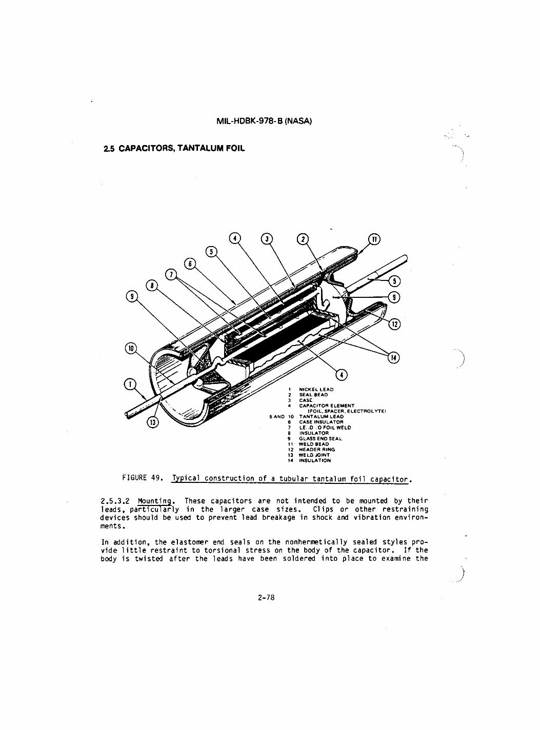
MIL-HDBK-978-B (NASA)
2.5 CAPACITORS, TANTALUM FOIL
5 ANO
NICKEL LEAD SEAL 8EAO CASC CAPACITOR ELEMENT
(FOIL. SPACER. ELECTROLYTE) TANTALUM LEAD CASE INSULATOR LEAOTO FOIL WELD INSULATOR GLASS END SEAL WELD BEAD HEADER RING WELD JOINT INSULATION
FIGURE 49. Typical construction of a tubular tantalum foil capacitor.
2.5.3.2 Mounting. These capacitors are not intended to be mounted by their leads, particularly in the larger case sizes. Clips or other restraining devices should be used to prevent lead breakage in shock and vibration environ-ments.
In addition, the elastomer end seals on the nonhermetically sealed styles pro-vide little restraint to torsional stress on the body of the capacitor. If the body is twisted after the leads have been soldered into place to examine the
2-78

MIL-HDBK-978- B (NASA)
2.5 CAPACITORS, TANTALUM FOIL
marking, it is quite possible that the foils will be torn away from the leads at the internal welds. This results in an open or intermittent capacitor. The smaller case sizes, and particularly the etched foil types, are especially susceptible to such mishandling. For this reason the capacitors should be assembled with the marking properly exposed.
2.5.4 Military designation.
2.5.4.1 Applicable military specification. Tantalum foil capacitors are covered by the following specification:
MIL-C-39006 CLR (established rellabll1ty) styles
2.5.4.2 Military type designations. The following is an example of a typical military callout, along with a description of the significance of each of the letters and digits in the designation. This is included only for reference in-formation.
Type designation example
CLR25 B D 600 G S
j : I _ i _ _ r _ _ i _ J _ . _ L Style Characteristic Voltage Capacitance Capacitance Type of Failure
tolerance seal rate level
2.5.5 Electrical characteristics.
2.5.5.1 Derating. The failure rate of tantalum foil capacitors under oper-ating conditions is a function of time, temperature, and voltage. Refer to MIL-STD-975 (NASA) for specific derating conditions.
2.5.5.2 End-of-life design limits. When operated under electrical and environ-mental conditions defined in the applicable military specification, the capaci-tance can be expected to change by ±15%. The leakage current can increase to 130% of the initial value.
2.5.5.3 Voltage ratings. The dc rated voltages for typical military styles are shown in Table IX.
2.5.5.4 Operating temperature range. These capacitors are suitable for opera-tion over a temperature range of -55° to +85°C with full rated voltage applied.
2.5.5.5 Reverse voltage. While it is advisable to operate polarized styles only in the forward direction, these units are capable of withstanding reverse voltages up to a value of 3 volts without damage. Nonpolarized styles may be operated at full rated voltage in either direction.
2-79

MIL-HDBK-978-B (NASA)
2.5 CAPACITORS, TANTALUM FOIL
TABLE IX. Voltage ratings
Style Anode Voltage Range (volts)
CLR25 Etched foil 15 to 150 CLR27 Etched foil 15 to 150 CLR35 Plain foil 15 to 450 CLR37 Plain foil 15 to 375 CLR71 Etched foil 15 to 150 CLR73 Etched foil 15 to 150
2.5.5.6 Ripple voltage. Tantalum foil capacitors are the only tantalum elec-trolytic capacitors capable of operating continuously on unbiased ac voltages. Nonpolarized styles may be operated continuously on an unbiased ac voltage with a peak value of 150 volts or the dc rating of the capacitor, whichever is less. Polarized styles must be biased to prevent dc voltage reversals.
However, in most applications, voltage is not the limiting factor. Except at relatively low frequencies, ripple is generally limited by the I. P loss in the capacitor. This loss is high because of the relatively high equivalent series resistance. The allowable ripple current is a function of case size, capaci-tance value, frequency, and ambient temperature.
When complex ripple wave shapes are involved they should be measured on an oscilloscope or by some other method which will give the peak rating. Tantalum foil capacitors should be limited to operation at ripple frequencies between 60 and 10,000 Hz. Above 10,000 Hz effective capacitance rapidly drops off to the point where these devices act as practically pure resistance at frequencies of only a few hundred kHz.
Figure 50 indicates maximum allowable ripple voltage and current for typical tantalum foil styles. This figure shows allowable rms values at 60 Hz and 25°C for the most popular case sizes, as a function of case size and capacitance value. Note that for etched foil styles, the values must be multiplied by 0.5.
The allowable ripple obtained from Figure 50 must then be multiplied by a fre-quency correction factor (Figure 51), and a temperature derating factor (Figure 52). Thus, for operation with an 800 Hz ripple frequency at 35°C ambient, the voltage or current value obtained from Figure 50 must be reduced by a factor of approximately 8.
2.5.5.7 DC leakage current. The leakage current of foil tantalum capacitors ranges from less than 1 uA to 100 uA or more depending on electrical rating, the type of construction, and temperature.
2-80

MIL-HDBK-978- B (NASA)
2.5 CAPACITORS, TANTALUM FOIL
CAPACITANCE IN MICRO FARADS
FIGURE 50. Maximum allowable ripple voltage and current for styles CLR25, CLR27. CLR35 & CLP37.
FIGURE 51. Correction factor for maximum allowable ripple current vs frequency for tantalum foil capacitors.
2-81

MIL-HDBK-978- B (NASA)
2.5 CAPACITORS, TANTALUM FOIL
CURV AND
'ES APPL>
ETCHED-f f TO BOTI =0IL UNIT
•1 PLAN rS
25 30 40 50 60 70 80 90 100 110 120 125 TEMPERATURE IN DEGREES
FIGURE 52. Correction factor for maximum allowable ripple voltage vs temperature for tantalum foil capacitors.
Leakage current, as in all tantalum capacitors, is the result of minute faults in the dielectric film. These faults tend to be self-healing under applied vol-tage, so that leakage current will normally decrease exponentially with life.
Leakage current is roughly proportional to applied voltage up to the maximum dc voltage rating.
Leakage current increases rapidly with temperature as shown in Figure 53. Note that leakage at 125°C is about 30 times the room temperature value.
2.5.5.8 Effects of frequency. Capacitance, dissipation factor or effective series resistance, and impedance will vary with the frequency of the applied voltage.
Capacitance vs frequency. Typical curves are shown in Figure 54 for frequencies up to 5 kHz.
2-82

MIL-HDBK-978- B (NASA)
2.5 CAPACITORS, TANTALUM FOIL
Z UJ {£ C D U UI C <
<
25 50 75 100 125 150 TEMPERATURE IN DEGREES CENTIGRADE
FIGURE 53, Typical curve, ratio of dc leakage current at rated voltage vs temperature for foil tantalum capacitors.
1 0 5
100
9 5
9 0
8 5
80
4 8 y F , 6 0 V - P
— P
l O y F , 3 0 V - P
^ ^ ^ N ^ ^ E W F , i o v-P ^ v ^ W H u F , 1 5 0 V - E
\ ^ 1 3 0 y F , 3 V - P
\ l 2U F, 7 5 V-E
1 1 1 1 ! 1 1 1 I I 1
- X ' * 50 V F 25V-E
N ^ 0 0 y F , 1 9 V - E
1 f i t
FREQUENCY IN KHz AT 25 C
FIGURE 54. Effect of frequency on capacitance of typical foil type tantalum capacitors.
2-83
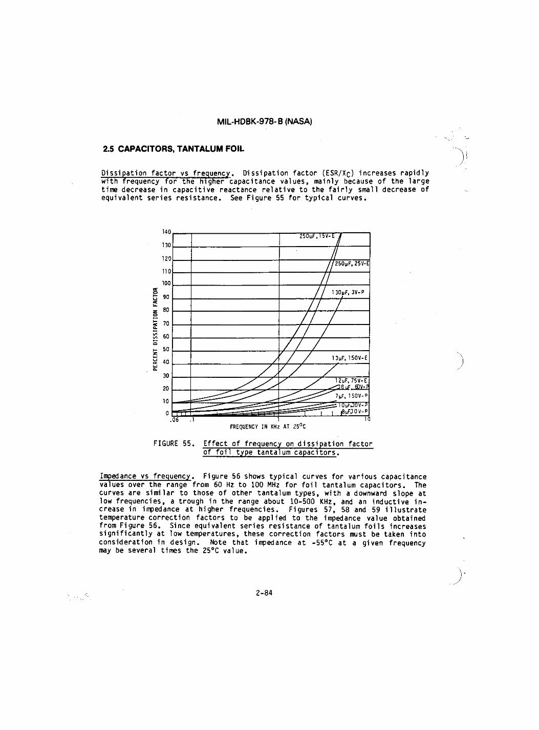
MIL-HDBK-978- B (NASA)
2.5 CAPACITORS, TANTALUM FOIL
Dissipation factor vs frequency. Dissipation factor (ESR/XQ) increases rapidly with frequency for the higher capacitance values, mainly because of the large time decrease in capacitive reactance relative to the fairly small decrease of equivalent series resistance. See Figure 55 for typical curves.
FIGURE 55. Effect of frequency on dissipation factor of foil type tantalum capacitors.
Impedance vs frequency. Figure 56 shows typical curves for various capacitance values over the range from 60 Hz to 100 MHz for foil tantalum capacitors. The curves are similar to those of other tantalum types, with a downward slope at low frequencies, a trough in the range about 10-500 KHz, and an inductive in-crease in impedance at higher frequencies. Figures 57, 58 and 59 illustrate temperature correction factors to be applied to the impedance value obtained from Figure 56. Since equivalent series resistance of tantalum foils increases significantly at low temperatures, these correction factors must be taken into consideration in design. Note that impedance at -55°C at a given frequency may be several times the 25°C value.
2-84

MIL-HDBK-978- B (NASA)
2.5 CAPACITORS, TANTALUM FOIL
10,000
2*r 1.000 8MF
2S*lF 100
¥i 2 SOfiF X 0 1
IOOMF m u z 10 < o III •l
SOOMF 2 J.OOO F
3.500MF
0.1
0.01
T1 UBULARS
/CSR
•G 100 1,000 10K 100K 1M 10M 100M FREQUENCY Hi
FIGURE 56. Impedance curves for tantalum foil capacitors at 25°Cy.
s . B U < 8
I -P ° 3 (Ii * C S » u
/ / / L -S5°C
J •30 T /
- , , 1
0 100 200 500 IK 2K BK 10K 20K 80K 0.1M 0.2M 0.5M 1M
FREQUENCY - HERT2
FIGURE 57. Tantalum foil impedance correction factors for capacitance up to t t t f:
2-85
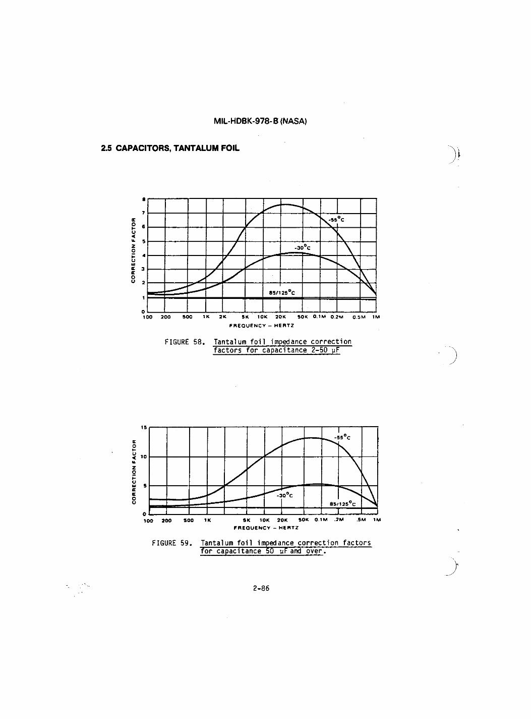
MIL-HDBK-978- B (NASA)
2.5 CAPACITORS, TANTALUM FOIL
8
7
6
5
4
3
2
1
0 100 200 500 1K 2K 5K 10K 20K 50K 0.1M 0.2M 0.5M 1M
F R E Q U E N C Y - H E R T Z
FIGURE 58. Tantalum foil impedance correction factors for capacitance 2-50 yF
S y - 5 5 °C
-3C l°C
85/1 2S°C
|
oc o H u < IL z o H U Ul cc AC o u
500 5K 10K 20K 50K 0 1M .2 M
F R E Q U E N C Y - H E R T Z
.5M 1M
FIGURE 59. Tantalum foil impedance correction factors for capacitance 50 yF and over.
2-86
MIL-HDBK-978- B (NASA)
2.5 CAPACITORS, TANTALUM FOIL
2.5.5.9 Circuit impedance. No special precautions are required with foil tantalum capacitor current limiting. These units will withstand sudden inrush and discharge currents without deleterious effects.
2.5.5.10 Series applications.
Series operation. Whenever tantalum capacitors are connected in series for higher voltage operation, a resistor should be paralleled across each unit. Unless a shunt resistor is used, the dc rated voltage can easily be exceeded on the capacitor in the series network with the lowest dc leakage current. To pre-vent capacitor destruction, a resistance value not exceeding a certain maximum should be used. This value will depend on capacitance, average dc leakage, and capacitor construction for plain foil types. The resistance across each capaci-tor should not exceed 5/C megohms, where C is in microfarads. For etched foil types use 15/C megohms.
Parallel operation. When tantalum foil capacitors are connected in parallel the sum of the peak ripple and the applied dc voltage should not exceed the recommended derated dc voltage rating of the capacitor with the lowest rating. The connecting leads of the capacitors in parallel should be large enough to carry the combined currents without reducing the effective capacitance due to series lead resistance.
2.5.6 Environmental considerations.
2.5.6.1 Stability and life. Tantalum electrolytic capacitors have excellent life and shelf life characteristics. Life, at higher temperatures will show a comparatively lower decrease in capacitance. With rated voltage applied, more than 4,000 hours of life can be expected at +85°C. These devices may be ex-pected to operate at least 1,000 hours at +85°C with less than 10 percent loss of capacitance.
Because the more stable tantalum film is less subject to dissolving by the sur-rounding electrolyte than the film in an aluminum capacitor, the shelf life of the tantalum unit is much longer, and less reforming is required. After storage for long periods, the reforming current required is low and the time required for reforming is comparatively short. Reforming may be expected to take less than 10 minutes. These properties are affected by the storage temperature to a significant degree, being excellent at temperatures from -55° to +25°C; good at +65° and relatively poor at +85°C.
2.5.6.2 Effects of temperature. The characteristics of these capacitors vary significantly with temperature, particularly with low temperatures.
Capacitance (C). Capacitance change with temperature is positive and depends on capacitance value and voltage rating. Capacitance change ranges from a maximum allowable of -20% to -40% at -55°C to an increase of +10 to +50% at maximum operating temperature.
2-87

MIL-HDBK-978- B (NASA)
2.5 CAPACITORS, TANTALUM FOIL
Equivalent series resistance (ESR). ESR increases rapidly at temperatures be-low 0° as shown in Figure 60 for a typical capacitor. It may also increase at temperatures over 80°C and voltages over 50 Vdc. Figure 61 depicts variation of impedance with temperature and frequency. The increase in impedance at -55°C in the mid frequencies is essentially due to an increase in ESR.
-25 O +25 +50 +75 +100 TEMPERATURE IN DEGREES CENTIGRADE
+125
FIGURE 60. Typical curves of impedance, capacitance, and equivalent series resistance with temperature" for 26-yF, 100-volt polarized etched-foil capacitors.
2.5.7 Reliability considerations. Foil tantalum capacitors properly used are the most reliable of the three types of tantalum capacitors. Unless subjected to electrical or mechanical overstress, the normal failure mode is by degrada-tion rather than a complete open or short.
2.5.7.1 Failure modes and mechanisms. Except for manufacturing defects, such as poor welds or improper end seals, a foil tantalum capacitor eventually fails by a decrease in capacitance beyond some acceptable limit. This results from vaporization of the electrolyte and its escape through the end seals, so that the capacitor dries out. Such failures are unlikely for several thousand hours of operation when used within their ratings.
2-88

MIL-HDBK-978- B (NASA)
2.5 CAPACITORS, TANTALUM FOIL
10
1.0
0.1
0.06
-
•53 I
IZ 2 -40°C > —
-20°C / o°c
-
-20°C / o°c
1 1 1 1 Mill i i i i IIII 1 1 1 1 III! 1 I 1 1 Ii III 1 1 1 1 Mil 10 100 FREQUENCY IN KHz
1M TOM
FIGURE 61. Typical curves of impedance with frequency at various temperatures for 200-yF, 6-volt plain-foil capacitors.
2.5.7.2 Screening. Established reliability specification MIL-C-39006 requires 100% operating voltage conditioning to screen out potential early life failures. Capacitors which exhibit excessive leakage are screened out as reliability hazards. For hermetically sealed types, a 100% seal test is also conducted.
Mounting. Clips or other restraining devices/methods should be used to prevent lead breakage and fatigue in shock and vibration environments.
2.5.7.3 Failure rate level determination. Consult MIL-HDBK-217 for current data on the particular style and quantative reliability level predictions.
2-89

MIL-HDBK-978- B (NASA)
2.6 CAPACITORS, SOLID TANTALUM
2.6 Solid tantalum.
2.6.1 Introduction. Solid tantalum capacitors are the most widely used elec-trolytic capacitors for electronics equipment. They have high volumetric efficiency, good stability with time and temperature, and are reliable devices when properly applied.
Because the electrolyte used is solid and dry, these capacitors have a more stable capacitance-temperature characteristic than any of the other electro-lytic capacitors. Maximum capacitance variation is less than 10% over the operating temperature range of -55°C to +125°C.
Their limitations are relatively high leakage current, possible dielectric punctures, limited voltage range available (6 to 100 volts), and a maximum allowable reverse voltage of 15 percent of the rated dc voltage at +25°C and only 1 percent at +125°C.
These capacitors are available in polarized and nonpolarized units under military type designations. ~
2.6.2 Usual applications. These capacitors . are generally used where low-frequency pulsating dc components are to be bypassed or filtered and where large capacitance values are required where space is at a premium, and where there are significant levels of shock and vibration. These capacitors are mainly designed for filter, bypass, coupling, blocking, energy storage, and other low voltage dc applications (such as transistor circuits in missile, computer, and aircraft electronic equipment) where stability, size, weight, and shelf life are important factors.
2.6.3 Physical construction. The anode consists of tantalum powder mixed with an organic binder and pressed into pellet form. The pellets are then sintered in a vacuum oven to decompose and evaporate the binder, yielding a pellet of high porosity and high surface area.
The pellets are anodized in an acidic bath to form the tantalum pentoxide dielectric on all surfaces reached by the electrolyte. The pellets are then impregnated with an aqueous solution of manganous salt, which is pyrolytically decomposed to yield manganese dioxide. The manganese dioxide is the working electrolyte in solid form. A carbon compound is applied over the surface of the manganese dioxide (Mn02) t 0 allow for application of a silver paint. The completed pellet is then inserted into a pool of molten solder inside the metal case which is then sealed. The solder is displaced up around the sides of the pellet to provide an electrical and mechanical bond to the case. Figure 62 shows the construction of a typical solid tantalum capacitor.
2-90
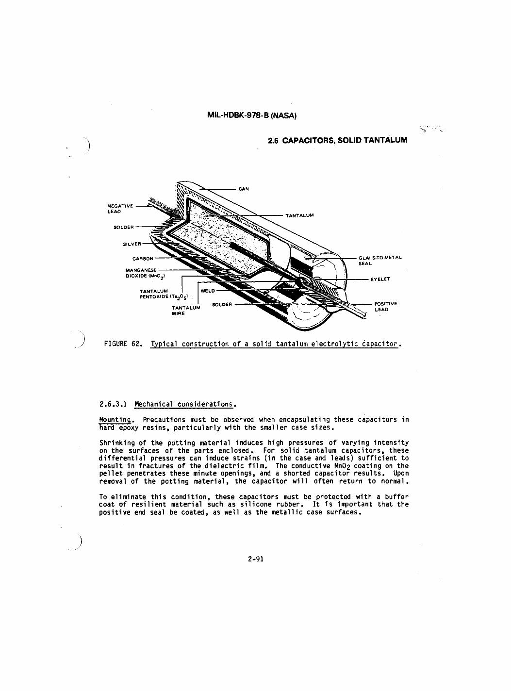
MIL-HDBK-978- B (NASA)
2.6 CAPACITORS, SOLID TANTALUM
GLASS-TO-METAL SEAL
- E Y E L E T
POSITIVE LEAD
FIGURE 62. Typical construction of a solid tantalum electrolytic capacitor.
2.6.3.1 Mechanical considerations.
Mounting. Precautions must be observed when encapsulating these capacitors in hard epoxy resins, particularly with the smaller case sizes.
Shrinking of the potting material induces high pressures of varying intensity on the surfaces of the parts enclosed. For solid tantalum capacitors, these differential pressures can induce strains (in the case and leads) sufficient to result in fractures of the dielectric film. The conductive Mn02 coating on the pellet penetrates these minute openings, and a shorted capacitor results. Upon removal of the potting material, the capacitor will often return to normal.
To eliminate this condition, these capacitors must be protected with a buffer coat of resilient material such as silicone rubber. It is important that the positive end seal be coated, as well as the metallic case surfaces.
2-91

MIL-HDBK-978- B (NASA)
2.6 CAPACITORS, SOLID TANTALUM
2.6.4 Military designation.
2.6.4.1 Applicab!e mi 1itary specification. Solid tantalum capacitors are covered by the following specification:
MIL-C-39003 Capacitors, Fi xed, Electrolyti c (Sol id Electro-lyte), Tantalum, Established Reliability, General Specification for.
2.6.4.2 Military type designation. The following is an example of a typical designation for an established reliability solid tantalum capacitor. For actual ordering reference, the latest issue of the applicable M39003 slash sheet must be consulted.
GSR13 B 565 <
T Style dc rated Capacitance Capac tance
voltage tolerance rate level
2.6.5 Electrical characteristics. These capacitors are available in three basic case configurations under MIL-C-39003. The CSR13 style is procured per specification sheet M39003/01, and the CSR09 style per M39003/02 and the CSR33 per M39033/06.
2.6.5.1 Voltage derating. Of all the electrolytic capacitors, the solid tanta-lums are the most stable over life and posses the lowest capacitance temperature characteristic. The limitations of the solid tantalum capacitors are relatively high leakage current (DCL), limited voltage range, and relatively low allowable reverse voltage.
When properly derated, these units may be operated over a temperature range of -55°C to +125°C. Refer to MIL-STD-975 (NASA) for specific derating conditions.
The failure rate of solid tantalum capacitors is a function of temperature, voltage, and circuit impedance. With each 10°C rise in operating temperature, the failure rate approximately doubles. The failure rate is also approximately proportional to the cube of the ratio of applied voltage to the rated voltage.
DC leakage current increases when either voltage or temperature are increased; the rate of increase is greater at the higher voltages and temperatures. A point can be reached where dc leakage current will avalanche causing the capaci-tor to be permanently shorted. For this reason the maximum ratings should never be exceeded and the derating guidelines should be observed.
2-92
MIL-HDBK-978- B (NASA)
2.6 CAPACITORS, SOLID TANTALUM
By increasing circuit impedance, the leakage current is reduced. In high-impedance circuits momentary breakdowns will self-heal. In low-impedance cir-cuits the self-healing characteristics under momentary breakdown of the dielec-tric do not exist. The large currents in low-impedance circuits may cause the capacitor to short.
To minimize the incidence of catastrophic shorts due to momentary dielectric breakdowns, and to allow self-healing action to take place, a series resistance of 3 ohms per applied volt should appear in series with the capacitor and its power source, or there should be limitations on the "turn-on" surge current. The charging current available to the capacitor should be one ampere or less. This need not be a discrete resistor at the capacitor terminals, but can in-clude the impedance of the power source and associated circuitry provided that no other large capacitors are directly in parallel with the one to be protected.
2.6.5.2 End-of-life design limits for solid tantalum capacitors. Expected capacitance change is ±10% and the leakage current change is 200% of initial limit.
2.6.5.3 Reverse voltage. These capacitors are capable of withstanding peak voltages in the reverse direction equal to 15 percent of their dc rating at +25°C, 10 percent at +55°C, 5 percent at +85°C, and 1 percent at +125°C.
2.6.5.4 Ripple voltage. These capacitors may be operated with an impressed ac ripple voltage, provided the capacitors do not exceed their heat dissipation limits. Total heat dissipation limits depend on the ambient operating tempera-ture and the operating frequency.
The individual detail specification should be consulted for maximum allowable ripple voltage at the frequency and temperature required. However, Figures 63 and 64 give typical ripple voltage limits for CSR13 styles.
In addition, the sum of the applied dc bias voltage and the peak of the ac ripple must not exceed the allowable rated dc voltage for the applicable tem-perature. The permissible ripple voltage may also be applied without a dc bias voltage, provided that the negative peak ripple does not exceed the allowable reverse voltage.
For example: Referring to Figure 63, a 10 yF capacitor of any voltage rating may be operated at 1.9 Vrms, 120 Hz, at 25°C; at 125°C the permis-sible voltage is reduced to 0.75 Vrms. When this same capacitor is sub-jected to a ripple frequency of 1000 Hz, the permissible ac must be reduced by a factor equal to the ratio of the allowable ripple at 1000 Hz, 25°C, (Figure 64) to the allowable ripple at 120 Hz, 25°C (Figure 63), i.e.,
Vrms (1000 Hz, 25°C) = 0.47 Vrms (Figure 63) 0.47
Vrms (1000 Hz, 125°C) = 0.75 (175") = 0-19 Vrms
2-93

MIL-HDBK-978- B (NASA)
2.6 CAPACITORS, SOLID TANTALUM
10
7 — '
N z 8
1 -o 1 -o > o -
< —
§ 00 -
.1 I I I I I III I I 1 1 1 1 1 1 1 I I 1 1 III
CAPACITANCE IN MICROFARADS
FIGURE 63. Permissible ripple voltage vs capacitance and ambient temperature at 120 Hz (style CSR13).
2.6.5.5 Series networks. When solid tantalum capacitors are connected in series, the maximum voltage across the series should not exceed the recommended derated voltage of the lowest rated capacitor in the group, or else voltage divider resistors should be used so that no capacitor in the group operates at more than its recommended derated voltage.
2.6.5.6 Parallel network. Whenever solid tantalum capacitors are connected in parallel, the sum of the peak ripple and applied dc voltage should not exceed the recommended derated voltage of the capacitor with the lowest rating.
2-94

MIL-HDBK-978- B (NASA)
2.6 CAPACITORS, SOLID TANTALUM
10
o S> CM
H < cN I--i O > S> < «/> ac
.01
j 1
1 1
\ \
1 1 1 1 1 1 II 1 1 1 M i l l 1 1 1 1 I N I
10 100 CAPACITANCE IN MICROFARADS
1,000
FIGURE 64. Permissible ripple voltage vs capacitance and frequency at 25°C (style CSR13).
To obtain a higher capacitance than that available from a single capacitor, a number of units may be connected in parallel. However, because of the peculiar failure mechanism associated with solid tantalum capacitors, this is not always a practical approach since each capacitor requires a resistance in series. Where there is no series impedance in the parallel legs and a minute break-down occurs, the parallel capacitors attempt to dump their charge into the low impedance fault. Thus, what might have been a clearing action may become a catastrophic failure.
2-95

MIL-HDBK-978- B (NASA)
2.6 CAPACITORS, SOLID TANTALUM
2.6.5.7 Dielectric absorption. Dielectric absorption may be observed by the reappearance of potential across the capacitor after it has been shorted and the short removed. This characteristic is important in RC timing circuits, triggering systems, and phase-shift networks. The curves shown in Figure 65 were established by charging capacitors for 1 hour at rated voltage and then discharging them through a dead short for 1 minute.
T IME - SECONOS
FIGURE 65. Typical dielectric absorption of sol id -electrolyte tantalum capacitors at 25°C.
Voltage recovery was measured with a high-impedance electrometer at the given intervals indicated on the curves. Increasing the ambient temperature shifts the curves to the left and decreases the amplitude but does not affect the shape. Shortening charge time, lengthening discharge time, or decreasing charging voltage results in reduction of the peak amplitude of the curve, but has little effect on its shape or relative position.
2.6.5.8 The solid tantalum capacitor as a circuit element. The equivalent circuit of the capacitor may be represented Tn simplified form as shown in Figure 66.
2-96

MIL-HDBK-978- B (NASA)
2.6 CAPACITORS, SOLID TANTALUM
FIGURE 66. Simplified equivalent circuit of a capacitor.
2.6.5.9 DC 1eakage current. DCL for solid tantalum capacitors at 25°C range from less than 1 uA in low capacitance values to about 20 iiA in the larger case sizes and capacitance values. Leakage current generally decreases with lower temperature, but increases by an order of magnitude at high temperature.
The shunt resistance, Rs, shown in Figure 66 represents the leakage path formed by an accumulation of individual faults in the tantalum pentoxide dielectric. These faults occur primarily because of a finite residue of impurities which remain in the tantalum metal despite the best practical purification techni-ques. Wherever an impurity is encountered, anodization cannot produce a con-tinuous Ta205 layer of uniform thickness. The result is a minute hole or thin spot in the dielectric layer that can be filled with the manganese dioxide (Mn02) solid electrolyte or with air. Compared with Ta205, either of these materials will allow relatively heavy conduction under conditions existing within the capacitor.
Simple probability dictates that the larger the capacitive area, the larger the number of impurity sites encountered, and the higher the leakage current. Actual leakage current in a given application is then a function of capacitance value, voltage rating, applied voltage, and temperature. Typical curves of leakage current vs applied voltage are shown in Figure 67 (A, B, and C).
2-97

MIL-HDBK-978- B (NASA)
2.6 CAPACITORS, SOLID TANTALUM
20
1 0 /
- /
/ + 8 5 ° C
1 / < a = / z : / V-ar « u —
§ —
- y ? + 2 5 ° C
. . 0 1
/
. 0 0 7 7 i i i 1 1 1 1 I I 1
9 0
10
1.0
1 5 1 0 1 5 2 0 3 0 3 5
VOLTS DC
-II 1 1 1
1 1 1
Azs°z
! / l I i 1 I l I 1 1 1
2 5 0 2 0 3 0 :
20
10
21.0
. 0 4
/ / /
+ 2 5 ° C >
/ 1 / j 1 l i l t
5 1 0 2 VOLTS DC VOLTS 0 C
A. Typical curves for 6.8 yF, 35 volt capacitor
B. Typical curves for 47 uF, 35 volt capacitor
C. Typical curves for 68 yF 20 volt capacitor
FIGURE 67. DC leakage current vs applied voltage for solid tantalum capacitor.
2-98

MIL-HDBK-978- B (NASA)
2.6 CAPACITORS, SOLID TANTALUM
2.6.5.10 Effects of frequency. Capacitance, effective series resistance, dis-sipation factor, and impedance all vary with the frequency of the applied volt-age. Usually the main concern will be the cumulative total effect of the equi-valent circuit, i.e., impedance. A brief discussion of each of these parameter variations follows:
Capacitance vs frequency. The rated capacitance value of these capacitors is specified as measured at 120 Hz. The apparent capacity decreases with frequency as shown in Figure 68.
H I H I
-
6 0 y F , 6 V
-
^ ^S^S^lOwf. ' - 15V 2 0 V
^ ^ ^ 1 5 0 y F . 5 5 V
-
^ ^ ^ h o O v F , 2 0 V
\ \ \ 4.7yF, 35V
i I I i i i i i i i i
\ / ^ 3 3 w F . 3 6 V
^ 2 2 y F , 3 5 V
1 1 1 1 1 1 J 1 . 0 6 .1 .12
FREQUENCY IN KHz
FIGURE 68. Capacitance vs frequency for typical solid tantalum capacitors at 25°C.
Dissipation factor vs frequency. Dissipation factor (ESR/Xc) is directly por-portional to frequency, and would theoretically be a straight line plot if R and C were ideal. Actual typical curves are shown in Figure 69.
2-99
MIL-HDBK-978- B (NASA)
2.6 CAPACITORS, SOLID TANTALUM
FIGURE 69. Dissipation factor vs frequency for typical solid tantalum capacitors at 25°C.
Impedance vs frequency. The impedance of a solifl tantalum capacitor at lower frequencies consists essentially of the combination of capacitive reactance and equivalent series resistance. As shown in Figure 70 thru 73, the initial downward slope of the curves is due primarily to capacitive reactance. The trough of the curves is almost totally resistive, and the self-inductance of the device no longer functions as a capacitor, and impedance increases with increasing frequency.
It can be seen that the troughs of the curves typically bottom out in the 500 kHz to 1 MHz range in the higher capacitance values, and that in the lower capacitance ranges (1 uF and less) the impedance curve tends to bottom out in the 1 to 10 MHz range. For these lower capacitance values, variation of impedance with frequency closely resembles that of paper capacitors.
It should be emphasized that the curves shown are typical. In design applica-tions where impedance over a particular frequency range is critical, special requirements may be in order. Actual impedance values, particularly at high frequencies, may vary significantly from the values shown on the curves.
2-100
MIL-HDBK-978-B (NASA)
2.6 CAPACITORS, SOLID TANTALUM
10
CO 21 X O
o 2: < Q
9= .10
1 1
1 Mil
l
/
+25°C \
-80°C +125°C
1 1
1 Mil
l
i i i inn
+125°C
1 III lltl 1 I I t II I 1 1 1 1 mi .1 10 100
FREQUENCY IN KHz
1M 10M
FIGURE 70. Typical curves of impedance vs frequency at various temper-atures for solid tantalum 330-uF, 6-volt capacitors.
2IJ •E O
o z < o
1 1
1 Mi
ll
Y -aouc
/ I / -40°c
/ / I / - +25°C > -
s \ X N J / ^NS^/tN/ 1
j^- +85°C
I— +125°C
1 1
1 1 I
II!
I M i mi 1 1 II III 1 II 1 Mil 1 1 1 1 Mil
FREQUENCY IN Hz
FIGURE 71. Typical curves of impedance vs frequency at various temper-atures for solid tantalum 68-pF, 20-volt capacitors.
2-101

MIL-HDBK-978- B (NASA)
2.6 CAPACITORS, SOLID TANTALUM
100
r -80°C
\ r -40°C
- .
r- +25°C
j- +80° C
\ r •12S°C
M
L 1 1 1 llll 1 III llll i i i IIIII i i 11mi 1 1 1 Mill
g 1.0
.IK IK 10K 100K FREQUENCY IN Hz
1M 10M
FIGURE 72. Typical curves of impedance vs frequency at various temper-atures for solid tantalum 6.8-yF, 35-volt capacitors.
10K 100K FREQUENCY IN Hz
FIGURE 73. Typical curves of impedance vs frequency at various temper-atures for solid tantalum 47-uF» 35-volt capacitors.
2-102

MIL-HDBK-978- B (NASA)
2.6 CAPACITORS, SOLID TANTALUM
2.6.6 Environmental considerations.
2.6.6.1 Effects of temperature. The capacitance of solid tantalum capacitors is relatively stable with temperature. This is also true of impedance, as shown in Figures 74 through 77.
TEMPERATURE IN DEGREES CENTIGRADE
FIGURE 74. Typical curves of impedance, capacitance, and equivalent series resistance vs. temperature for 330-yF, 6-volt capacitors. "
2.0
x R
8i.o £ ••
.8
IMPEDAN ICE
m • m
CAPACIT- ANCE ^ E 1QUIVALI ENTSERI ESRESIS1 L A
rANCE I
-80 -50 -25 0 425 *50 *?5 TEMPERATURE IN OEGREES CENTIGRADE
4100 • 125
FIGURE 75. Typical curves of impedance, capacitance, and equivalent series resistance vs. temperature for 68°yF, 20-volt capacitors.
2-103

MIL-HDBK-978- B (NASA)
2.6 CAPACITORS, SOLID TANTALUM
T E M P E R A T U R E IN DEGREES CENT IGRADE
FIGURE 76. Typical curves of impedance, capacitance, and equivalent series resistance vs. temperature for 6.8-yF, 35-volt capacitors.
T E M P E R A T U R E IN DEGREES C E N T I G R A D E
FIGURE 77. Typical curves of impedance, capacitance, and equivalent series resistance vs. temperature for 47- uF, 35-volt capacitors.
2-104

MIL-HDBK-978- B (NASA)
2.6 CAPACITORS, SOLID TANTALUM
2.6.6.2 Operating temperature range. These capacitors are suitable for opera-tion over a temperature range of -55° to +85°C at full rated voltage.
2.6.6.3 Effects of temperature on failure rate. Failure rate approximately doubles with each 10°C rise in operating temperature.
2.6.7 Reliability considerations.
2.6.7.1 Failure modes. A solid tantalum capacitor is subject to two primary failure modes; open or intermittent internal connections and shorted dielec-tric. Other possible failure modes include change in capacitance or dissipa-tion factor with operation, and an increase in leakage current beyond certain limits.
Leakage current changes, even up to 100%, would not normally be significant in applications of these capacitors. In fact, leakage current normally decreases during initial hours of operation, tending to remain constant or decreasing slightly thereafter. Similarly, changes in capacitance and dissipation factor are small enough to present no real problem in normal applications.
Open or intermittent conditions are usually the result of discrete manufactur-ing defects, such as loose slugs due to inadequate soldering, poor internal welds, or solder shorts.
The primary failure concern in solid tantalum capacitors then, is the short circuit, which usually constitutes a catastrophic circuit failure as well as a capacitor failure.
2.6.7.2 Failure mechanism. As discussed under leakage current, all solid tantalum capacitors have faults in the dielectric because of a residue of impurities.
Each impurity site in the dielectric produces leakage current when a conductive material is present. Leakage currents would be many times larger than they are, if it were not for a change in Mn02 structure that takes place opposite the fault sites. As dc voltage is applied to the capacitor, high current densities are produced in the faults. The high current produces heating in the Mn02 opposite the fault. At elevated temperature, Mn02 undergoes spontaneous reduc-tion to lower oxides. The lower oxides coincidentally display much higher elec-trical resistivities, effectively reducing the leakage current that originally produced the heating.
If a relatively small fault site is encountered, the mechanism just described may permanently reduce the leakage current associated with that site to a very low value. Since this process can continue indefinitely in service, the capacitor tends to improve with age.
2-105

MIL-HDBK-978- B (NASA)
2.6 CAPACITORS, SOLID TANTALUM
Failure is believed to occur because relatively large impurities migrate to the anode-dielectric interface during operation. This action creates defects which are too large to be self-healing. The amount of current flow may be sufficient to produce localized heating which destroys a still larger area of dielectric. Since the oxides of manganese have a negative temperature coeffi-cient of resistivity, excess temperature rise in the defect zone can cause loss of control of leakage current. This leads to thermal runaway and catastrophic failure. Since the migration rate is temperature dependent, the failure rate is also temperature dependent.
Because of this inherent thermal runaway problem* solid Tantalum capacitors should not be used in power supply filter applications or other applications where the effective series resistance is less than one ohm per volt.
For Grade 1 applications* additional surge current testing 1s required as outlined in MIL-STD-975.
2.6.7.3 Screening. To screen out manufacturing defects and potential early life failures, the following screening tests are usually performed: temperature cycling, operating voltage conditioning, vibration, surge current at -55°, +25° and +85°C and X-ray.
2.6.7.4 Reliability derating. The failure rate of solid tantalum capacitors under operating conditions is a function of time, temperature, and voltage. Refer to MIL-STD-975 (NASA) for specific derating conditions.
2.6.7.5 Failure rate determination. For actual quantitative prediction pur-poses, current failure rate data should be consulted for the part as procured to a particular specification, style, and reliability level. For further informa-tion, refer to MIL-HDBK-217.
2-106
MIL-HDBK-978- B (NASA)
2.7 CAPACITORS, WET SLUG TANTALUM
^2.7 Wet slug tantalum.
2.7.1 Introduction. The liquid electrolyte sintered-anode tantalum elec-trolytic capacitor, commonly known as the "wet slug," was the first type of tantalum capacitor to be developed for large-scale production. The outstanding advantage of the wet-slug type is its high volumetric efficiency. For capacitance values in the microfarad range, it will generally pro-vide the smallest case size available in a given voltage rating. However, it has two outstanding disadvantages. It cannot tolerate reverse voltage of any magnitude for even short periods of time, and its electrolyte, which is a sulfuric acid solution in liquid or gel form, is highly corrosive and can damage neighboring circuitry if it leaks out. For these reasons, these capacitors should be considered nonpreferred styles. First consideration should always be given to solid or foil type tantalum capacitors. Wet-slug capacitors should be used only when the required function can be filled by no other available style. Recently, the CLR 79, MIL-C-39006/2? has been added to MIL-C-39006. This unit is identical to the CLR 65 except that the case is all tantalum rather than silver, it has a three-volt dc reverse capability, and a high permissible ripple current capability than other wet-slug capacitors.
Due to the all-tantalum construction of the part, there is nc silver migration. Electrical specifications are included in MIL-STD-975 (NASA).
)zm7.2 Usual applications. These capacitors are used mainly in power supply filter circuits. They are available as single-cell units with voltage ratings to about 125 Vdc, and in multiunit series or series-parallel packages with ratings to several hundred volts. They are strictly polar devices and are not available in a nonpolar configuration because of their extreme sensitivity to voltage reversal.
2.7.3 Physical construction. The anode consists of a slug formed by press-ing and sintering tantalum powder into a porous cylindrical structure. This slug is then electrochemically treated to form a coating of tan-talum pentoxide on all the surfaces of the granules. The anodized film serves as the capacitor dielectric, and the thickness of the film deter-mines the voltage rating. The slug, with a tantalum wire lead extending, is assembled into a drawn case which serves as the cathode. The case is filled, and the slug impregnated with a highly conductive electrolyte, usually a dilute sulfuric acid solution in gel form.
The electrolyte serves as the connection between the dielectric film and the cathode. The case is sealed at the positive end, and a solderable lead is butt-welded to the tantalum lead emanating from the end seal.
2-107

MIL-HDBK-978- B (NASA)
2.7 CAPACITORS, WET SLUG TANTALUM
Until recently these capacitors were available only in a nonhermeti-cally sealed style, the end seal consisting of a combination of Teflon and elastomer bushings and 0-rings which were compressed and retained by crimping the case (see Figure 78). While this type of seal is normally quite effective over temperature extremes, extended temperature cycling will often cause elec-trolyte leakage.
ANOOELEAD G R O O V E IN B U S H I N G
LIP O F C A S E C R I M P E D I N T O O - R I N G
E L A S T O M E R O - R I N G
A N O D E -
I ky.7-r.v.v.
[;>yi,
T E F L O N BUSHING
A N O D E A N D S E A L END O F C A P A C I T O R
E L A S T O M E R O - R I N G
G R O O V E IN BUSHING
' C A S E C R I M P E D INTO O - R I N G
• S I L V E R C A S E
- A C I D E L E C T R O L Y T E
I N S U L A T O R
• C A T H O D E L E A D
FIGURE 78. Typical construction of an elastomer seal design.
Hermetically sealed styles, such as MIL type CLR65, are also available and are shown in Figure 79. This type of construction eliminates the problem of exter-nal leakage but the capacitor is still subject to failure by leakage of elec-trolyte past the inner seal. Displacement of electrolyte past the Teflon seal into the area of the adjacent glass seal will result in a high leakage path between the postive lead and the case.
2-108

MIL-HDBK-978- B (NASA)
2.7 CAPACITORS, WET SLUG TANTALUM
A N O D E L E A D
H I G H - T E M P E R A T U R E S O L D E R ( W E L D F O R C L R 7 9 )
E X T E R N A L G L A S S - T O - M E T A L W E L D / H E R M E T I C S E A L
E L A S T O M E R S E A L
W I R E - T O - P E L L E T WELI
F I N E S I L V E R C A S E ( T A N T A L U M CASE F O R C L R 7 9 )
C A T H O D I C E T C H
I L t P t I
K - J
m r —- — -t r » i « i _ \ i \ i ^ m r —- — -t r » i « i _ \ i \ i ^
• P T F E S E A L
• G E L L E D E L E C T R O L Y T E
S P A C E R
W E L D
C A T H O D E L E A D
FIGURE 79. Typical construction of a hermetically sealed wet-slug tantalum capacitor. '
2.7.4 Mi 1itary designation. Wet-slug tantalum capacitors are covered by the fol1 owing specification:
MIl-C-39006 Established Reliability. Styles CLR 65 and CLR 79 covers the hermetically sealed types, Figure 80.
2-109

MIL-HDBK-978-B (NASA)
2.7 CAPACITORS, WET SLUG TANTALUM
T E R M I N A L S O L D E R E D O R W E L D E D T O C A S E
° | *)f °
£2222 C A S E C I R C U I T D I A G R A M
FIGURE 80. Outline drawing of a hermetically sealed capacitor.
2.7.5 Electrical characteristics.
2.7.5.1 Ratings. These capacitors are available as single units in voltage ratings up to about 125 Vdc, and in capacitance values to about 600 uF, de-pending on the voltage rating. They are also available in packaged units, consisting of several individual capacitors in parallel or series. Parallel arrangements are at ratings to several thousand microfarads at low voltages, and to about 10 pF at 600 Vdc. These ranges are also covered by the pre-ferred solid or foil types, though usually at some increase in size.
2.7.5.1.1 Derating. The failure rate of wet-slug tantalum capacitors under operating conditions is a function of time, temperature and voltage. Refer to MIL-STD-975 (NASA) for specific derating conditions.
2.7.5.2 Reverse voltage. These capacitors, with the exception of the CLR 79 which has a 3 volt reverse capability at 85°C, cannot be operated with any re-verse bias. The capacitor will fail in a short time due to silver plating action.
2-110
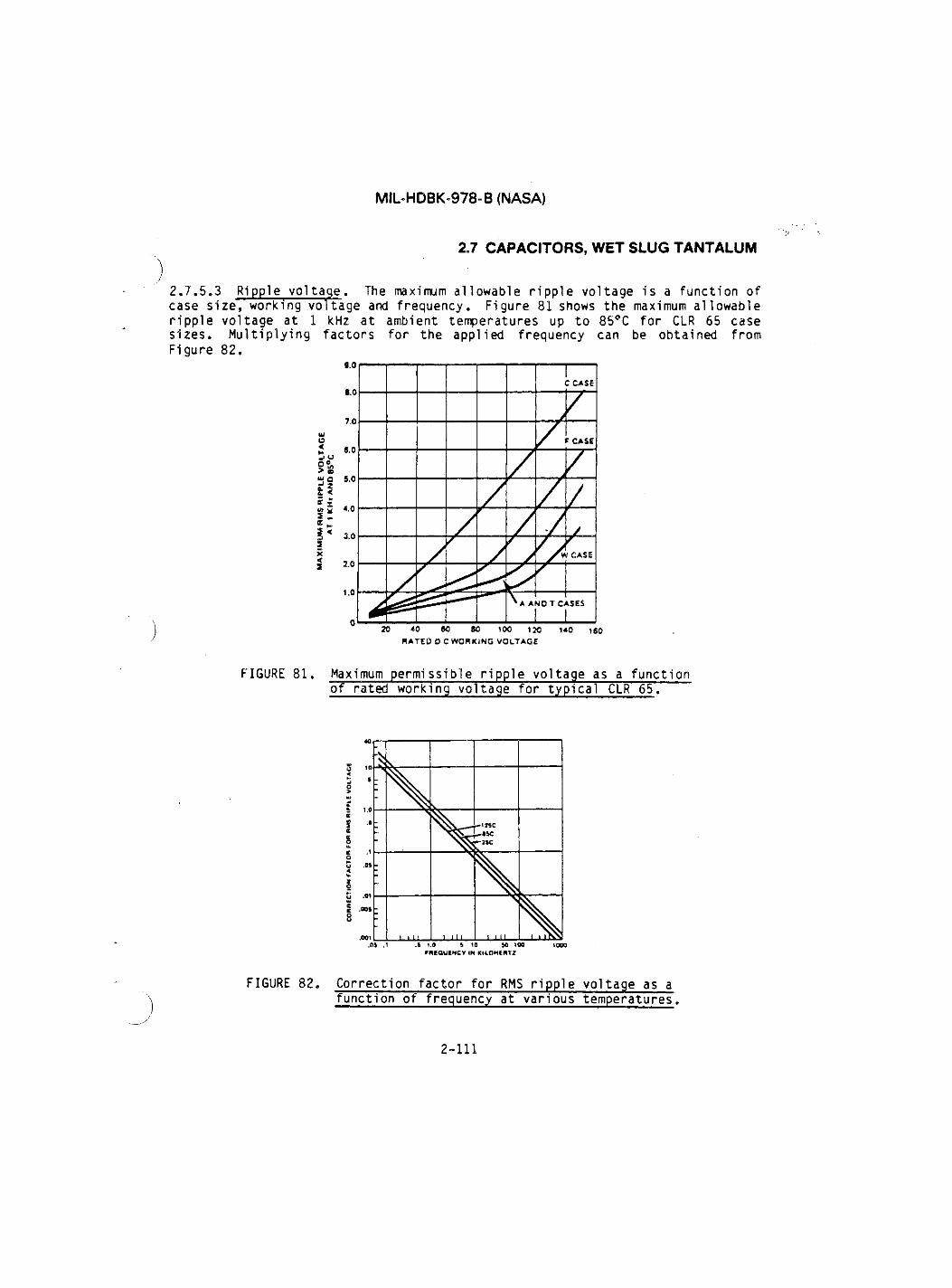
MIL-HDBK-978- B (NASA)
2.7 CAPACITORS, WET SLUG TANTALUM
2.7.5,3 Ripple voltage. The maximum al lowable ripple voltage is a function of case size, working voltage and frequency. Figure 81 shows the maximum allowable ripple voltage at 1 kHz at ambient temperatures up to 85°C for CLR 65 case sizes. Multiplying factors for the applied frequency can be obtained from Figure 82.
9.0
8.0
7.0 UJ 0 2 e.o J U > « W O 5.0 * 5 1 £ ^ 5 4.0
I X
I 2.0
1.0
20 40 60 SO 100 120 140 160 RATED D C WORKING VOLTAGE
FIGURE 81. Maximum permissible ripple voltage as a function of rated working voltage for typical CLR 65.
;
: -125C ^asc •**2SC
- \ ;
1111 I MI 1 U J \ .OS .1 .6 <.0 $ 10 SO 100 1000
FREQUENCY IN KI10MCRT2
FIGURE 82e Correction factor for RMS ripple voltage as a function of frequency at various temperatures.
2-111

MIL-HDBK-978- B (NASA)
2.7 CAPACITORS, WET SLUG TANTALUM
2.7.5.4 Ripple currents. Figures 83 through 86 represent a number of typical temperature rise vs. rms ripple current plots for various capacitance/voltage case sizes (CLR 79).
G O O
r
H 09 m <40 B H B 3 H € X W 20 ft. i H
j
/ -
J m — 3 . G / 4 F / 1 2 5 U i I Z O H x
— l O / i F . S O U , 1 2 0 H z
— 3 . 6 / i F , 1 2 S U , 4 0 X H z
- 1 0 / i F « S O U ! 4 0 K H z
/ -
200 4 0 0 S O O B O O
R I P P L E C U R R E N T I N mAr-mi
l O O O 1 2 0 0 1 4 0 0
FIGURE 83. Case T1 temperature rise as a function of ripple current,
GO
200 4 0 0 G O O 8 0 0 l O O O
R I P P L E C U R R E N T I N mAr-mm
1200 1 4 0 0
FIGURE 84. Case T2 temperature rise as a function of ripple current.
2-112
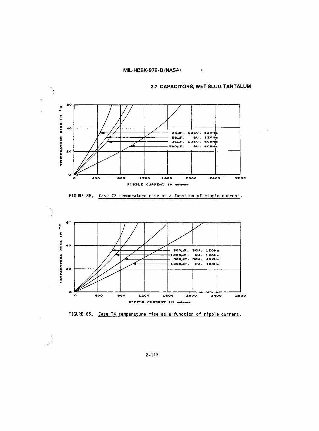
MIL-HDBK-978- B (NASA)
2.7 CAPACITORS, WET SLUG TANTALUM
©
GO
u s 3 h € K 20 U ft,
2S/iF ,
5fe/iF ,
25/iF ,
S60/iF ,
12SUi 120Hz I 120Hz
12SU, 40XHz
6U , I 40KHz
400 800 1200 1600 2000 RIPPLE CURRENT I 14 mAr>m«
2400 2800
FIGURE 85. Case T3 temperature rise as a function of ripple current.
u ©
M W M
K H K 5 N € 06 H fik
60
40
20
*00 800 1200 1SOO 2000
RIPPLE CURRENT IN niArms
2400 28DO
FIGURE 86. Case T4 temperature rise as a function of ripple current.
2-113

MIL-HDBK-978- B (NASA)
2.7 CAPACITORS, WET SLUG TANTALUM
2.7.5.5 DC leakage current. Leakage current of wet-slug capacitors is quite low, in the order of a few uA or less at room temperature and rated voltage. Leakage current increases by approximately an order of magnitude at maximum rated temperature.
2.7.5.6 Power factor and equivalent series resistance. The power factor of wet-slug capacitors measured at standard conditions (120 Hz, 25°C) ranges from allowable maximum values of about 2% to 60%, depending on capacitance and voltage rating. This order of magnitude is typical of all types of electroly-tic capacitors and is usually of little concern in typical filtering applica-tions. At low temperatures, however, equivalent series resistance increases rapidly. This effect, in combination with a typical correspondingly large decrease in capacitance at low temperatures, may require a capacitor of large nominal value to be selected for proper circuit operation over the temperature range. (Figure 87).
T E M P . IN DEGREES CENTIGRADE TEMP. IN DEGREES CENTIGRADE
FIGURE 87. Typical curves of equivalent series resistance as a function of temperature (all voltage ratings shown are 85°C ratings).
2-114

MIL-HDBK-978- B (NASA)
2.7 CAPACITORS, WET SLUG TANTALUM
Figure 88 is a plot of equivalent series resistance (ESR) vs frequency for various case sizes. When capacitors are to be used in circuits operating between 10 kHz and 100 kHz, impedance measurements at 40 kHz (CLR 79) should be considered as a screening requirement.
FIGURE 88. Effects of frequency on ESR.
2.7.5.7 Effect of frequency. Figures 89 and 90 show typical curves of impedance vs frequency and temperature for wet-slug capacitors. The effect of capacitance decrease and ESR increase at low temperature is readily apparent.
2-115
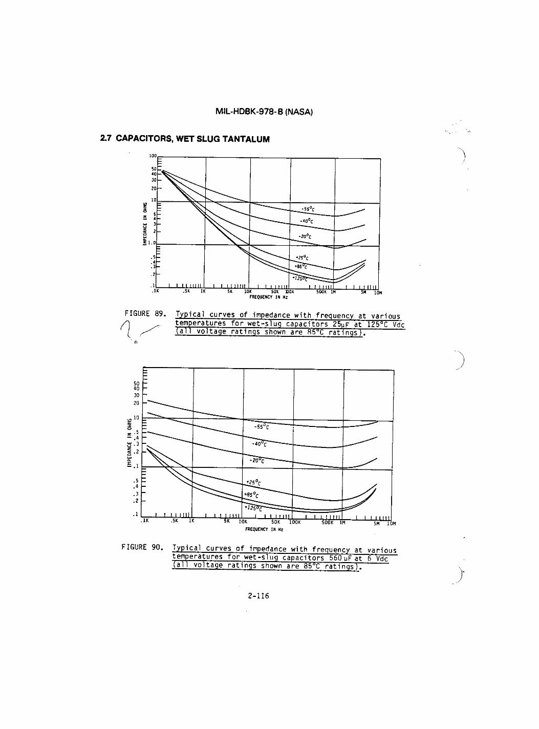
MIL-HDBK-978- B (NASA)
2.7 CAPACITORS, WET SLUG TANTALUM
2C X o
0 o - ^ N v o -
J \ 4 -3 -2 -
n
-40°C
m20°C
5 I i -3-? —
I 1 I 11 Mill ... 1 I I Mill! 1 1 1 Mill
^ E — ^
I 1 1 Mil i i 11 mi FREQUENCY IN Hz
FIGURE 89. Typical curves of impedance with frequency at various temperatures for wet-slug capacitors 25yr at 125°C Vdc (all voltage ratings shown are 85°C ratings
FIGURE 90. Typical curves of impedance with frequency at various temperatures for wet-slug capacitors 560 uF at 6 Vdc (all voltage ratings shown are 85°C ratings).
2-116

MIL-HDBK-978- B (NASA)
2.7 CAPACITORS, WET SLUG TANTALUM
" 2.7.5.8 Circuit impedance. There are no particular limitations on wet-slug tantalum capacitors with respect to inrush current. There is some evidence to indicate that repeated discharge into a low impedance load may have a cumulative degrading effect. Sudden discharge of these devices sometimes results in the generation of transient reverse voltages. Since exposure to reverse voltage will cause these capacitors to fail, operation under conditions where such discharges may occur should be avoided.
2.7.6 Environmental considerations.
2.7.6.1 Effects of temperature. At low frequencies, the capacitance of these devices will decrease by about 15 to 65%, depending on rating. Equivalent, series resistance also increases rapidly at low temperatures (Figures 87 and 91).
2.7.6.2 Temperature cycling. Repeated temperature cycling will usually result in electrolyte leakage in a high percentage of elastomer-sealed wet-slug-c'apaci-tors. This will often result in no apparent decrease of capacitance or some other functional degradation of the capacitor itself, but the corrosive electro-lyte may damage adjacent circuitry. Depending on the type and quality of the seal and the severity of the temperature excursions, leakage may occur in as few as 5 or 6 cycles, or may not occur until 100 or more cycles.
There is some evidence that electrolyte leakage is aggravated by exposure to low j temperatures in test chambers cooled by CO2.
Sulfuric acid has an affinity for carbon dioxide, and will readily absorb it if negative internal pressure developed at low temperatures allows passage of the gas into the electrolyte. Then, as the temperature is raised, expansion of the absorbed CO2 generates a positive pressure inside the capacitor case and forces electrolyte out past the seal. Thus, it is possible that some of the failures observed in temperature cycling are artifically accelerated. In any event, the hermetically sealed style should always be specified when wet-slug capacitors are used.
2.7.6.3 Shock and vibration. As with other capacitor types, component speci-fication vibration tests are always conducted with the body of the capacitor securely mounted. For high levels of shock and vibration, these capacitors may require supplementary mounting, particularly in the larger case sizes.
2.7.7 Reliability considerations.
2.7.7.1 Failure modes and mechanisms (see Table X). According to most manufac-turers1 descriptions, the predominant failure mode of elastomer-sealed wet-slug capacitors is gradual loss of capacitance with operation, and an ultimate open circuit condition. This is the result of the gradual vaporization of the elec-trolyte past the seal into the surrounding atmosphere. The rate of electrolyte loss is directly affected by the capacitor temperature. With the decrease in capacitance there is concurrent increase in ESR, again because of electrolyte
\ loss.
2-117

MIL-HDBK-978- B (NASA)
2.7 CAPACITORS, WET SLUG TANTALUM
N Z 0 N
T
H OS
H z « H 5 « € g
1 . 5
-SO - 2 S O +25 +SO +75 +100 +125
TEMPERATURE IN DEGREES CELSIUS
+75 +100 +125
TEMPERATURE IN DEGREES CELSIUS
FIGURE 91. Typical curves of capacitance as a function of temper-ature (all voltage ratings shown are 85°C ratings).
2-118

MIL-HDBK-978- B (NASA)
2.7 CAPACITORS, WET SLUG TANTALUM
TABLE X. Failure nodes and mechanisms (CLP 65 style)
Failure Mechanism
Description/Cause Detection Method Method to Minimize | or Eliminate Cause
Elec-trolyte leakage
Faulty crimping of elastomer seals, riser wire out of round or has scratches and abrasions.
Thymol blue or litmus paper test. Increase in dissipation factor or decrease in capacitance. Temperature cycling, burn-in, seal test, insulation resistance.
Use of hermetically sealed capacitor design; use gelled electrolyte to mini-mize mobi1ity.
Leakage past inner seal causing elec-trolyte to bridge anode lead to cathode.
Increased leakage cur-rent or short circuit. Temperature cycling, burn-in.
Use of hermetic capac-itors having fully anodized anode riser through the seal and external nickel lead attachment.
Silver deposi-tion on anode
Reverse voltage on capacitor.
High leakage current, lower ESR, short cir-cuit.
Application must ensure voltage is never reversed during use or test. Minimize ripple current. Use of designs utilizing titanium or tantalum cases.
Mechan-ical defects
Warped slugs, slugs cocked in case, canted seals, bent or improper length risers, etc.
Radiographic inspec-tion.
Improved process con-trol .
For a properly manufactured and screened device that has not been mishandled during test inspection and that has never been subjected to reverse voltage, even of a transient nature, the above failure mode is probably the most likely. However, failure analysis experience indicates that the main problem source for this device is application of reverse voltage.
Since the tantalum pentoxide dielectric is a rectifier, the film conducts in the direction of the reverse voltage and can be damaged or destroyed, depending on the magnitude and duration of the reverse voltage. In addition, reverse current causes electroplating of silver from the case onto and beneath the oxide layer. This increases the current leakage paths, resulting in increased dissipation and
\ internal heat rise, liberation of gases, and catastrophic failure. The forma-/tion of hydrogen and oxygen gases at the electrodes creates excessive internal
pressure and can result in electrolyte leakage or bursting of the case.
2-119

Mll-HDBK-978- B (NASA)
2.7 CAPACITORS, WET SLUG TANTALUM
Although these devices are capable of some self-healing action, voltage rever-sals introduce an incipient failure mechanism which is largely unpredictable. The final effect of reverse bias depends on the magnitude of the voltage and time of application, since the amount of plating action is a coulombic function. The voltage threshold is very low, and levels of less than 100 mv have caused failure, given enough time. In addition, there appears to be no practical way of testing these capacitors to determine whether they have been subjected to short-time reversals.
Reverse polarity can be applied in several ways, even from the terminals of an ohmeter during part inspection, board tests, or tests at the subsystem or system level. In addition, reverse polarities have been applied at some unsus-pected operational phase, such as during system turn-on or stand-by position, interactions of failures or removal of other parts, power line transients, etc.
For these reasons, these devices must be used with a full knowledge of their limitations.
2.7.7.2 Screening. Temperature cycling and operational voltage conditioning are the most commonly used screening techniques for these capacitors. Temper-ature cycling is used to screen out units with improper or defective seals, as evidenced by electrolyte leakage. Voltage conditioning helps to detect units with improperly formed or contaminated anodes. Forward dc leakage current on a good unit will normally decrease to some value and remain relatively constant, or continue to decrease at a lower rate with continued operation. Measurements on a potential failure will tend to show an increase in leakage current. These devices should be subjected to vibration screening to eliminate devices that exhibit voltage spikes (5 to 20 volts) observed at 20 g and 80 g axial vibration and 51 g random vibration.
2.7.7.3 Reliability derating. The failure rate of wet-slug tantalum capaci-tors under operating conditions is a function of time, temperature and voltage. Where wide temperature variations are expected on a continual basis throughout the life of the system, solid or foil tantalum capacitors should he specified. If a wet-slug tantalum capacitor must be used, the hermetically sealed type should be specified.
Since present designs of hermetically sealed depend on an elastomer seal to pre-vent internal electrolyte leakage of the capacitor itself, reliability derating should be considered from the temperature cycling standpoint. When wet tantalum capacitors are connected in parallel, the sum of the peak ripple and the applied dc voltage should not exceed the recommended derated dc voltage rating of the capacitor with the lowest rating. The connecting leads of the capacitors in parallel should be large enough to carry the combined currents without reducing the effective capacitance due to series lead resistance.
2.7.7.4 Failure rate. For purposes of reliability predictions, MIL-HnRK-217 should be consulted. Since the failure rate of these devices depends so greatly on the conditions to which they have been exposed and transient conditions which they may see, published failure rate data based on controlled conditions of operation must be treated mainly as a base for predicted performance.
2-120

MIL-HDBK-978- B (NASA)
2.8 CAPACITORS, VARIABLE
^ 2 . 8 Variable.
2.8.1 Introduction. Variable capacitors are not included in MIL-STD-975 (NASA); they are included in this handbook to provide a technical understanding of this type of part.
Variable capacitors are small-sized trimmers designed for use where fine tuning adjustments are periodically required during the life of the equipment. The three types most popularly used are the piston tubular trimmer, ceramic dielec-tric, and air trimmer.
2.8.2 Usual applications. The variable capacitor is normally used for trimming and coupling in such circuits as intermediate frequency, radio frequency, oscil-lator, phase shifter, and discriminator stages. Because of their low mass, these units are relatively stable against shock and vibration, which tend to cause changes in capacitance.
2.8.3 Physical construction.
2.8.3.1 Piston type, tubular trimmer. These capacitors are constructed of glass or quartz dielectric cylinders and metal tuning pistons. A portion of the cylinder is plated with metal and forms the stator. The metal piston (con-trolled by a tuning screw) acts as the rotor.
.JThe overlap of the stator and the rotor determines the capacitance. The self contained piston within the dielectric cylinder functions as a low inductance coaxial assembly. The piston type capacitor is further classified as a rotating or nonrotating piston type.
2.8.3.2 Rotating piston. The rotating piston is constructed in such a way as to secure the piston to the tuning screw. As the tuning screw is rotated the piston rotates with it (Figure 92).
2.8.3.3 Nonrotating piston. The nonrotating piston is constructed so that the tuning screw is secured at each end and cannot move up and down as it is turned. The screw is threaded into the piston and the piston moves up and down without rotating (Figure 93).
2.8.3.4 Ceramic dielectric trimmer. This capacitor consists of a single rotor and stator for each section, with each section fabricated of ceramic material impregnated with transformer or silicone oil. Pure silver is fired and burn-ished on the top of the base of the stator in a semicircular pattern. The rotor (usually of titanium dioxide) has pure silver contact points. The contact surfaces of both the rotor and stator are ground and lapped flat, eliminating air space variations with temperature. (See Figure 94).
2-121
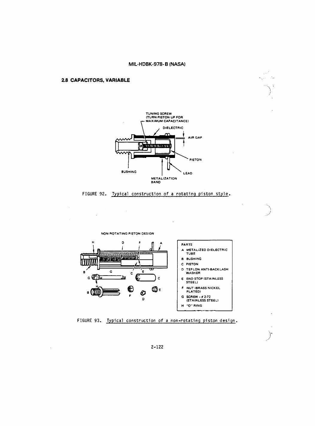
MIL-HDBK-978- B (NASA)
2.8 CAPACITORS, VARIABLE
T U N I N G S C R E W ( T U R N P I S T O N UP F O R
M E T A L I Z A T I O N B A N D
FIGURE 92. Typical construction of a rotating piston style.
N O N R O T A T I N G P I S T O N O E S I G N
H 0 P A R T S
A M E T A L I Z E D D I E L E C T R I C T U B E
B B U S H I N G
C P I S T O N
0 T E F L O N A N T I - B A C K L A S H W A S H E R
E E N D S T O P ( S T A I N L E S S S T E E L )
F N U T ( B R A S S N I C K E L P L A T E D )
G S C R E W - it 2 - 7 2 ( S T A I N L E S S S T E E L )
H " O " R I N G
FIGURE 93. Typical construction of a non-rotating piston design
2-122

MIL-HDBK-978- B (NASA)
2.8 CAPACITORS, VARIABLE
FIGURE 94. Outline drawing of a ceramic dielectric variable capacitor.
2.8.3.5 Air dielectric trimmer. This capacitor consists of multiple rotors and stators, each having a half-moon shape. The overlap of rotors and stators determine the capacitance. The rotors can be rotated continuously and full capacitance change occurs during each 360° rotation. (See Figure 95).
FIGURE 95. Outline drawing of a variable air dielectric trimmer.
2.8.3.6 Mounting. The trimmer capacitors are generally leaded devices and may be mounted close to a metal panel with little increase in capacitance. Care should be exercised to avoid cracking or chipping the ceramic mounting base.
2.8.4 Military designation. Variable capacitors are covered by MIL-C-81 for variable ceramic, MIL-C-92 for variable air and MIL-C-14409 for piston type tubular. The following examples show typical military designations for variable capacitors.
2-123

MIL-HDBK-978- B (NASA)
2.8 CAPACITORS, VARIABLE
2.8.4.1 MIL-C-81 (variable ceramic dielectric).
CV11 A
I Style Characteristic
070
Capacitance
2.8.4.2 MIL-C-92 (variable air dielectric).
06 n
I 004
Style Voltage Capaci itance I
Rotational Life
2.8.4.3 MIL-C-14409 (variable piston type tubular)
PC51 - H
I 380
Capaci tance Style Character!stic
2.8.5 Electrical considerations.
2.8.5.1 Voltage^ratings. The MIL-C-81, "CV" type capacitors are available to" 500 Vdc from -55°C to +85°C with voltage derating to 125°C.
The MIL-C-92, "CT" type capacitors are available in a range of voltages to 700 Vdc from -55°C to +85°C.
The MIL-C-14409, "PC" types capacitors are available in a range of voltages to 1250 Vdc from -55°C to +125°C and with characteristic letter "Q" from -55°C to +150°C.
2.8.5.2 Available capacitance values. Variable ceramic dielectric capacitors are available in a range of capacitance values from approximately 1.5 to 60 pF with a DF of 0.2 percent maximum.
Variable air dielectric capacitors are available in a range of capacitor values from approximately 1.3 to 7.5 pF with a Q greater than 1500 at 1 MHz.
Variable piston type tubular capacitors are available in a range of capacitance values from 0.5 to 120 pF with Q ranging from 10,000 to 250, inversely propor-tional to the capacitance value.
2-124

MIL-HDBK-978- B (NASA)
2.8 CAPACITORS, VARIABLE
2.8.5.3 Q vs frequency. The Q of a trimmer capacitor depends on the dielec-tric system and the size of the unit. The internal mechanism and plating do not affect it. The RF current flows along the unit to the base, providing a long inductive path which decreases Q and lowers the self-resonant frequency. Typi-cal self-resonance of glass trimmer capacitors varies from 100 MHz to 1000 MHz according to size and construction. A quick comparison of the characteristics of a ceramic trimmer and a glass tubular trimmer shown in Table XI.
Table XI. Comparison of characteristics of ceramic and glass trimmer
Characteristic Ceramic Glass
Tuning Resolution Temperature Range Temperature Coefficient Capacitance Drift DCWV Q Rotational Life
1/2 turn To +85°C 200 to 1200 ppm/°C 75% or 0.5 pF To 500 Vdc 500 at 1 MHz 100 Turns
Multi-turn To +125°C ±50 ppm/°C 0.01 to 0.1 pF To 1200 Vdc 1000 at 20 MHz Up to 10,000 Turns
\ 2.8.5.4 Derating. The failure rate of variable capacitors under operating con-yditions is a function of time, temperature and voltage.
2.8.5.5 End-of-life design limits for variable capacitors. Expected capaci -tance change is ±5 percent from set value and Insulation Resistance change is -30 percent from initial value.
2.8.6 Reliability considerations.
2.8.6.1 Failure modes and mechanisms. The trimmer capacitors have had a reliable history of electrical operation. Most of the problems associated with the parts are of a mechanical nature. Rough handling will cause shorting of the plates of an air trimmer. Cracking of the rotor or stator of the ceramic trimmer during improper soldering or cleaning methods can allow solder flux onto the walls of a piston type, thereby binding the piston or fracturing the screw adjust.
2.8.6.2 Screening. Early life failures are best screened out by a voltage con-ditioning period of 50 hours or more under voltage stress. Tubular trimmers are typically burned-in at 100% of rated voltage while ceramic trimmers can be burned-in at 200% of rated voltage. Temperature cycling is also specified prior to voltage conditioning to accelerate failure of parts with mechanical weaknesses or poor internal connections.
2.8.6.3 Failure rate determination. For failure rate information refer to MIL-HDBK-217.
2-125

2.8 CAPACITORS, VARIABLE
MIL-HDBK-978- B (NASA)
THIS PAGE INTENTIONALLY LEFT BLANK
2-126
MIL-HDBK-978-B (NASA)
3.1 RESISTORS, GENERAL
3. RESISTORS
3.1 General.
3.1.1 Introduction, This section contains information on the various types of resistors intended for use in NASA applications.
The information in this section is designed to help the engineer select the resistors he will specify. As with other types of components, the most impor-tant thing a user must decide is which of the numerous types of resistors will be best for use in the equipment he is designing. Proper selection is the first step in building reliable equipment. To properly select the resistors to be used, the user must know as much as possible about the types from which he can choose. He should know their advantages and disadvantages, their behavior under various environmental conditions, their construction, and their effect on circuits and the effect of circuits on them. He should know what makes resis-tors fail. He should also have an intimate working knowledge of the applicable military specification.
All variable and fixed resistors can be grouped into one of three general basic types. They are composition, film, or wirewound types (see Figure 1). The composition type is made of a mixture of resistive material and a binder which are molded into the proper shape and resistance value. The film type is com-posed of a resistive film deposited on, or inside of, an insulating cylinder or filament. The wirewound type is made up of resistance wire which is wound on an insulated form. These basic types differ from each other in size, cost, resistance range, power rating, and general characteristics. Some are better than others for particular purposes; no one type has all of the best character-istics. The choice among them depends on the requ-irements, the environment and other factors which the designer must understand. The designer must realize that the summaries of the following general characteristics and costs are rela-tive, not absolute, and that all the requirements of a particular application must be taken into consideration and compared with the advantages and drawbacks of each of the several types before a final choice is made.
The detailed requirements for standard resistor types are contained in the applicable military specification and applicable subsection of this section.
3.1.2 Applicable military specifications.
Mil Spec Title
MIL-STD-202 Test Methods for Electronic & Electrical Components Parts
MIl-HDBK-217 Reliability Prediction of Electronic Equipment
3-1

MIL-HDBK-978-B (NASA)
3.1 RESISTORS, GENERAL
Ml L-R-39007 MIL-R-39009 MIL-R-39005 SVMBOL RWR SYMBOL RER SYMBOL: R8R
RESISTORS ESTABLISHED REL IAB IL ITY {ADJUSTMENT TYPE)
RESISTORS ESTABLISHED REL IAB IL ITY {ADJUSTMENT TYPE)
WIRE WOUND NON WIRE WOUND
Ml L-R-39015 SYMBOL: RTR
Ml L-R-39035 SYMBOL: RJR
Ml L-R-83401 SYMBOL: RZ
RESISTORS SPECIAL 1 RESISTORS SPECIAL
NETWORKS FIXED FILM THERMAL
Ml L-T-23648 SYMBOL: RTH
FIGURE 1. Resistor categories.
3-2
MIL-HDBK-978- B (NASA)
1 3.1 RESISTORS, GENERAL
MIL-STD-790
MIL-STD-1276
MIL-R-39008
MIL-R-55182
MIL-R-39017
MIL-R-39005
MIL-R-39007
MIL-R-39009
MIL-R-39015
MIL-R-39032
MIL-R-39035
MIL-R-83401
MIL-R-23648
GSFC-S-311-P18
Reliability Assurance Program for Electronic Parts specifications
Leads for Electronic Components Parts
Fixed Composition
Fixed Film (High Stability)
Fixed Film (Insulated)
Fixed Wire-wound (Accurate)
Fixed Wire-wound (Power Type)
Fixed Wire-wound (Power Type, Chassis Mounted)
Variable Wire-wound (Lead Screw Actuated)
Resistors, Package of
Variable Nonwire-wound (Adjustment Type)
Fixed, Film Resistor Networks
Thermistor (Thermally Sensitive, Resistor) Insulated
Thermistor (Thermally Sensitive, Resistor) Insulated, NTC
3.1.3 General definitions, A list of common terms used in rating and design application of resistors follows.
3.1.3.1 Resistors, general.
Ambient operating temperature. The temperature of the air surrounding an object, neglecting small localized variations.
Critical value of resistance. For a given voltage rating and a given power rating, this is the only value of resistance that will dissipate full rated power at rated voltage. This value of resistance is commonly referred to as the critical value of resistance. For values of resistance below the critical value, the maximum voltage is never reached; and for values of resistance above critical value, the power dissipated becomes lower than rated. Figure 2 shows this relationship.
3-3

MIL-HDBK-978- B (NASA)
1 3.1 RESISTORS, GENERAL
Dielectric strength. The breakdown voltage of the dielectric or insulation of the resistor when the voltage is applied between the case and all terminals are tied together. Dielectric strength is usually specified at sea level and at simulated high air pressures.
Hot-spot temperature. The maximum temperature measured on the resistor due to both internal heating and the ambient operating temperature. Maximum hot-spot temperature is predicted on thermal limits of the materials and the design. The hot-spot temperature is also usually established as the top temperature on the derating curve at which the resistor is derated to zero power.
Insulation resistance. The dc resistance measured between all terminals con-nected together and the case, exterior insulation, or external hardware.
Maximum working voltage. The maximum voltage stress (dc or rms) that may be applied to the resistor is a function of the materials used, the required per-formance, and the physical dimensions (see Figure 2).
Noise. An unwanted voltage fluctuation generated within the resistor. Total noise of a resistor always includes Johnson noise which is dependent on resis-tance value and temperature of the resistance element. Depending on type of element and construction, total noise may also include noise caused by current flow and noise caused by cracked bodies and loose end caps or leads. For vari-able resistors, noise may also be caused by jumping of the contact over turns of wire and by an imperfect electrical path between contact and resistance element.
Standard resistance value. The resistance value tabulated by a decade chart is specified in the applicable military specification. Resistance values not listed in the chart for the appropriate tolerance are considered as nonstandard for that specification.
£ o UJ P O W E R - C O N S T A N T -
R A T E D . P V 0 L T A G E - C O N S T A N T -R A T E D , E
Q.
\ V « ? r \
\ \
\
R E S I S T A N C E V A L U E I N C R E A S I N G
FIGURE 2. Maximum working voltage and critical value of resistance.
3-4
MIL-HDBK-978-B (NASA)
3.1 RESISTORS, GENERAL
/ Resistance tolerance. The permissible deviation of the manufactured resistance value (expressed in percent) from the specified nominal resistance value at standard (or stated) environmental conditions.
Stabi1ity. The overall ability of a resistor to maintain its initial resist-ance value over extended periods of time when subjected to any combination of environmental conditions and electrical stresses.
Temperature coefficient (resistance temperature characteristies). The magni-tude of change in resistance due to temperature; Tt is usually expressed i n percent per degree centigrade or parts per million per degree centigrade (ppm/°C). If the changes are linear over the operating temperature range, the parameter is known as "temperature coefficient (TC)"; if nonlinear, the para-meter is known as "resistance temperature characteristic."
Voltage coefficient (resistance voltage characteristic). Certain types of re-sistors exhibit a variation of resistance entirely due to changes in voltage across the resistor. This characteristic is the voltage coefficient; it is generally applicable to resistors of 1,000 ohms and over.
3.1.3.2 Resistors, variable.
x End resistance. The resistance measured between the wiper terminal and an end J terminal with the wiper element positioned at the corresponding end of its
mechanical travel.
Noise. The effective contact resistance introduced in the wiper arm while rotating the wiper across the resistor element. Wirewound potentiometers are normally referred to in terms of equivalent noise resistance (ENR) which is caused primarily by variations in wiper contact during travel along the wire element. Although nonwirewound potentiometers have a continuous resistor element, there is usually a built-in dc offset due to measurable contact resistance between the wiper and the resistor. Their noise is therefore nor-mally referred to in terms of contact-resistance variation (CRV) which is caused primarily by the changes in contact resistance between the wiper and the resistor element during rotation.
Resolution or adjustability. The ability of an operator to predetermine ohmic value, voltage, or current. This is a measure of the sensitivity or degree of accuracy to which a potentiometer may be set. Wirewound potentiometers, having noncontinuous elements, are typically referred to in terms of a theoretical resolution which is the reciprocal of the number of turns of wire. Adjusta-bility is affected by the material and the uniformity of the resistor and the wiper elements, the length of the resistor element, and the design of the ad-justment mechanism.
Rotational life. The number of cycles of rotation which can be attained at certain operating conditions while remaining within specified allowable para-
\ metric criteria. A cycle comprises the travel of the wiper along the total y resistor element in both directions.
3-5

Mil-HDBK-978-B (NASA)
3.1 RESISTORS, GENERAL
Setting stability. The ability of a potentiometer to maintain its initial setting during mechanical and environmental stresses, it is•normally expressed as a percentage change in output voltage with respect to the total applied voltage.
Torque. The mechanical moment of force applied to a potentiometer shaft. Starting torque is the maximum torque required to initiate shaft rotation. Stop torque is the maximum torque which can be applied to the adjustment shaft at a mechanical end-stop position.
Total resistance. The resistance measured between the two end terminals of a potentiometer.
Travel. The clockwise or counterclockwise rotation of the wiper along the resistor element. Mechanical travel is the total rotation of the wiper between end-stop positions. Electrical travel is the rotation between maximum and minimum resistance values. These are not identical owing to discontinuities at the end positions.
3.1.3.3 Resistor network, fixed, film.
Aspect ratio. The geometical relationship of the length and width (L/W) of a rectangular resistor element which is used in the layout of networks to estab-lish "as fired" resistance values (e.g., when L = W, the aspect ratio is 1:1, or 1 "square."
DIP. Dual-in-line-package.
Formulation. A specific mix of thick-film material where the conductor, glass, and other additive ingredients are formulated to provide certain properties such as a specific sheet resistivity or TCR.
Paste/ink. Screenable thick-film material comprised of metals, oxides, and glasses in an organic vehicle which when fired, produces a circuit element such as a resistor or conductor.
Power density. The power dissipation per unit area of a resistor or substrate (in watts per square inch) used to determine the optimum layout design of a network.
Screen. The process of printing a network pattern of thick-film ink or paste onto a substrate by means of a squeegee applied to a photoetched wire-mesh "silk screen" or metal mask.
Sheet resistivity. The nominal resistance per unit area of a thick-film ink or paste which is usually expressed in ohms per square inch (assuming a constant thickness) where the design resistance value of the screened resistor is deter-mined by R = p L/W.
3-6

MIL-HDBK-978- B (NASA)
1 3.1 RESISTORS, GENERAL
Substrate. The base or carrier for the thick-film network which is usually a ceramic plate.
Thick-fi1m/cermet/metal glaze. Resistor and conductor materials comprised of metals or metal oxides in a glass binding system which can be screened onto a substrate and fired to provide circuit elements or networks.
Tracking. The inherent capability of resistors from the same formulation and screened onto the same substrate to exhibit similar performance characteristics (e.g., drift, TCR).
Trim/abrade/adjust. The process of tailoring a thick-fiIm-resistor element to a specific value or tolerance by the removal of resistor material (by means of sandblasting or laser abrading) which increases the ohmic value.
Voltage gradient/field strength. The linear voltage stress applied across a resistor element (in volts per inch) used to determine the optimum geometry of a high-voltage resistor.
3.1.3.4 Resistors, thermal.
\ Current-time characteristic. The relationship, at a specified ambient tempera-J ture, between the current through a thermistor and time elapsed from the appli-
cation of a step function of voltage.
Dissipation constant (a). The ratio, at a specified ambient temperature, of change in power dissipation in a thermistor to the resultant body temperature change.
Maximum operating temperature. The maximum body temperature at which a ther-mistor will operate for an extended period of time with acceptable stability of its characteristics. This temperature is the combination of external and in-ternal self heating.
Maximum power rating. The maximum power rating of a thermistor is the maximum power which a thermistor will dissipate for an extended period of time with acceptable stability of its characteristics.
Negative temperature coefficient (NTC). An NTC thermistor is one in which the zero-power resistance decreases with an increase in temperature.
Positive temperature coefficient (PTC). A PTC thermistor is one in which the zero-power resistance increases with an increase in temperature.
3-7

MIL-HDBK-978- B (NASA)
1 3.1 RESISTORS, GENERAL
Resistance ratio. The ratio of the zero-power resistances of a thermistor measured at two specified reference temperatures.
R£ Ro
(11) = e6 JL- JL (12) T1 T2
where: Ro (Ti) is the resistance at absolute temperature Ti.
Ro (T2) is the resistance at absolute temperature T2.
e is 2.718.
6 is a constant which depends on the material used to make the thermistor.
Stability. The ability of a thermistor to retain specified characteristics after being subjected to environmental and/or electrical test conditions.
Standard reference temperature. The thermistor body temperature at which nomi-nal zero-power resistance is specified.
Temperature-wattage characteristic. The relationship, at a specified ambient temperature, between the thermistor temperature and the applied steady-state wattage.
Thermistor. A thermally sensitive resistor whose primary function is to exhibit a change in electrical resistance with a change in body temperature.
Thermal time constant (T). The time required for a thermistor to change 63.2% of the difference between its initial and final body temperature when subjected to a step function change in temperature under zero-power conditions.
Zero-power resistance (Ro). The resistance value of a thermistor at a speci-fied temperature with zero electrical power dissipation.
Zero-power resistance temperature characteristic. The relationship between the zero-power resistance of a thermistor and its body temperature.
Zero-power temperature coefficient of resistance (err). The ratio at a speci-fied temperature, T, of the rate of change of zero-power resistance with tem-perature to the zero-power resistance.
a T = KdRT) R (dT)
3.1.4 NASA standard parts. See the introduction Section 1.1 for a complete description of the NASA Standard Parts Program. In addition to this handbook, the principal elements of this program include MIL-STD-975.
3-8

MIL-HDBK-978- B (NASA)
1 3.1 RESISTORS, GENERAL
b. Nominal minimum resistance tolerance available is ±0.1 percent for fixed, film resistors and ±1.0 percent for the resistor networks.
c. Maximum practical full-power operating ambient temperature should not exceed 125°C for metal film RNC types and 70°C for RLR resistors Type RZ resistor networks are continuously derated from 70°C to 125°C.
d. Operation at rf (above 100 MHz) may produce inductive effects on spiral-cut type fixed, film resistors, and capacitive effects on the resistor networks.
e. The resistance temperature characteristic is fairly low (±200 ppm/°C) for thick-film types (RLR) and very low (±25 ppm/°C) for metal-film types.(RNC). The resistance temperature characteristic is fairly low (±300 ppm/°C, ±100 ppm/°C and ±50 ppm/°C) for resistor networks (RZ).
f. Electrostatic effects should be considered since resistors can change value when subjected to electrostatic charges. Resistors with a tolerance of 0.1 percent should be packaged in accordance with MIL-R-39032.
3.1.5.3 Fixed, wirewound (accurate) resistors, RBR.
a. Fixed, wirewound, accurate resistors are physically the largest of all types for a given resistance and power rating. They are very conser-vatively rated and are available in standard tolerances as low as ±0.02 percent.
b. They are used where high cost and large size are not critical and operational climate can be controlled.
c. Application of voltages in excess of voltage rating may cause insula-tion breakdown in the thin coating of insulation between element coating.
d. Operation above 50 kHz may produce inductive effects and intrawinding capacitive effects.
e. The resistance element is quite stable within specified temperature 1i mi ts.
f. Use of good soldering techniques is extremely important since higher contact resistance may cause overall resistance shifts far outside of resistance tolerance on low value units.
g. The presence of moisture may degrade coating or potting compounds.
3-155

MIL-HDBK-978- B (NASA)
1 3.1 RESISTORS, GENERAL
MIl-STD-975 is a standard parts list for NASA equipment with section 10 contain-ing a summary of standard resistors.
These parts all use basic military ordering references conforming to the type designation according to the applicable military specification for the respec-tive part as described in the paragraphs of this section.
3.1.5 General device characteristies.
3.1.5.1 Fixed, composition resistors, RCR.
a. The nominal minimum resistance tolerance available for fixed, composi-tion resistors is ±5 percent. Combined effects of climate and opera-tion on unsealed types may raise this tolerance to ±15 percent from the low value (i.e., aging, pressure, temperature, humidity, voltage gradient, etc.).
b. High-voltage gradients will produce resistance change during opera-tion.
c. High Johnson noise levels at resistance above 1 megohm preclude use in critical circuits of higher sensitivity.
d. Radio frequency will produce end-to-end shunted capacitive effects because of short resistor bodies and small internal distances between both ends.
e. Operation at VHF or higher frequency reduces effective resistance due to losses in the dielectric (the so-called Boella effect).
f. Exposure to humidity may have two effects on the resistance value. Surface moisture may result in leakage paths which will lower the resistance values or absorption of moisture into the element may increase the resistance. These phenomena are more noticeable in higher values of resistance.
When exposed to a humid atmosphere while dissipating less than 10% of rated power or in shelf storage, nonoperating equipment, and shipping conditions, resistance values may change as much as 15%. Before being considered failures, out of tolerance resistors should be conditioned in a dry oven at 100 ±5°C for 48 hours.
Resistors which continue to be out of tolerance after conditioning should be considered failures.
3.1.5.2 Fixed, film resistors, RNC, RLR, and fixed, film networks, RZ.
a. These resistors are low tolerance, high stability, low environmental changes, low temperature coefficient, space and weight saving, and low noise.
3-156

MIL-HDBK-978- B (NASA)
1 3.1 RESISTORS, GENERAL
3.1.5.4 Fixed, wirewound resistors (power type), RER and RWR. This type resis-tor is generally not supplied in low tolerances and its frequency response is poor. However, its temperature coefficient is low.
3.1.5.5 General characteristics of variable resistors, RJR and RTR.
a. All types of variable resistors should be derated for operation above their rated ambient temperature.
b. Wirewound types should not be used in frequency-sensitive rf circuits due to introduction of inductive and capacitive effects.
c. High humidity conditions may have a deleterious effect on unenclosed types due to the resistance shift in composition types and winding-to-winding shorts in wirewound types.
d« Nonwirewound elements may wear away after extended use leaving par-ticles of the elements to permeate the mechanism and resulting in warmer operation, high-resistance shorts, etc. Wirewound types are subject to noise because of stepping of the contact from wire-to-wire.
e. With either wirewound or nonwirewound resistors, good practice indi-cates the use of enclosed units to keep out as much dust and dirt as possible and to protect the mechanism from mechanical damage. The presence of oil through lubrication may cause dust or wear particles present to concentrate within the unit.
f. Select a variable resistor with a power rating sufficient to handle the higher current produced when the resistor is reduced, particu-larly if it is being used in series as a voltage-dropping resistor.
g. When a variable wirewound linear resistor is being used as a voltage divider, the output voltage through the wiper will not vary linearly if current is being drawn through it. This characteristic is usually called the "loading error." To reduce the loading error, the load resistance should be at least 10 to 100 times as great as the end-to-end potentiometer resistance.
h. No current should be drawn from the wiper of a nonwirewound resistor.
3.1.6 General parameter information. Resistors must be selected to be compat-ible with the conditions to which they are exposed. Numerous factors must be considered in this selection process. The most important are noted in the following:
3.1.6.1 Resistance value. These are initially determined by the circuit requirements. Usually these values need to be adjusted to make them closely match the standard resistance values supplied by the manufacturer, or listed in the military specifications. If it is impossible to adjust circuit values to a standard value, parallel or series combination resistors can be used.
3-11

MIL-HDBK-978- B (NASA)
1 3.1 RESISTORS, GENERAL
The design engineer should also remember that the resistance value of the resistor that is put into the physical circuit will differ from the value he has on his circuit schematic. This difference will change as time passes. The purchase tolerance of the resistor to be used will allow it to differ from the nominal stated value, depending on the type of resistor specified. Further-more, the temperature at which the resistor works, the voltage across it, and the environment it encounters will affect the actual value at particular times. For example, the designer should allow for a possible variation of ±15 percent from the nominal value of a purchased ±5 percent composition resistor if he expects his circuit to continue to operate satisfactorily over a very long time under moderate ambient conditions. Such a figure is a rule of thumb based on many tests and most resistors will remain much nearer their starting value; but if many are used, chance will ensure that some will go near this limit.
3.1.6.2 Power rating. The minimum required power rating of a resistor is another factor that is initially set by the circuit usage but is markedly affected by the other conditions of use. As mentioned previously, the power rating is based on the hot-spot temperature the resistor will withstand while still meeting its other requirements of resistance variation, accuracy, and life.
Self-generated heat. Self-generated heat in a resistor is calculated as P = I^R. This figure, in any circuit, must be less than the actual power rating of the resistor used. It is practice to calculate this value and to use the next larger power rating available in the standard. This calculation should, how-ever, be considered only as a first approximation of the actual rating to be used.
Rating versus ambient conditions. The power of a resistor is based on a cer-tain temperature rise from an ambient temperature-of a certain value. If the ambient temperature is greater than this value, the amount of heat that the resistor can dissipate is correspondingly reduced, and therefore it must be derated because of temperature. All military specifications contain derating curves to be used for the resistors covered.
Rating versus accuracy. Because of the temperature coefficient of resistance that all resistors possess, a resistor which is expected to remain near its measured value under conditions of operation must remain cool. For this rea-son, all resistors designated as accurate are very much larger physically for a certain power rating than are ordinary "nonaccurate" resistors. In general, any resistor, accurate or not, must be derated to remain very near its original measured value when it is being operated.
Rating versus life. If especially long life is required of a resistor, partic-ularly when "life" means remaining within a certain limit of resistance drift, it is usually necessary to derate the resistor even if ambient conditions are moderate and if accuracy by itself is not important. A good rule to follow when choosing a resistor size for equipment that must operate for many thou-sands of hours is to derate it to one-half of its nominal power rating. Thus,
3-12
MIL-HDBK-978- B (NASA)
1 3.1 RESISTORS, GENERAL
if the self-generated heat in the resistor is 1/3-watt, do not use a 1/2-watt resistor, but rather a 1-watt resistor. This will automatically keep the resistor cooler, will reduce the long-term drift, and will reduce the effect of the temperature coefficient. For equipment demanding small size but with a relatively short use life, this rule may be impractical. The engineer should adjust his dependence on rules to the circumstances at hand. A "cool" resistor will generally last longer than a "hot" one and it can absorb overloads that might permanently damage a "hot" resistor.
Rating under pulsed conditions and under intermittent loads. When resistors are used in pulse circuits, the actual power dissipated during the pulses can some-times be much more than the maximum rating of the resistor. For short pulses the actual heating is determined by the duty factor and the peak power dissi-pated. Before approving a resistor application, the engineer should be sure that: (1) the maximum voltage applied to the resistor during the pulses is never greater than the permissible maximum voltage for the resistor being used, (2) the circuit cannot fail in such a way that continuous excessive power can be drawn through the resistor and cause it to fail, (3) the average power being drawn is well within the agreed-on rating of the resistor, and (4) continuous steep wavefronts applied to the resistor do not cause any unexpected troubles.
3.1.6.3 Derating. With the exception of failures due to "random" occurrences resulting from manufacturing defects or overstress, resistor failure rate is a function of time, temperature, and applied power. Operational life can be significantly lengthened by power derating and by limiting the operating ambient temperature.
The extent to which electrical stress (e.g., voltage, current, and power) is derated depends upon temperature. The general interrelationship between elec-trical stress and temperature is shown in Figure 3. The approved operating conditions lie within the area below the derated limitation line (ESdr). Opera-tion at conditions between the derated limitation line and the maximum specifi-cation curves results in lower reliability (see MIL-HDBK-217). Operation in this reduced reliability area requires specific approval.
Numerical values are applied to the curves for each part type based on a per-centage of the device manufacturer's maximum rated values. The applicable derating curve or derating percentages are specified in MIL-STD-975.
3.1.6.4 Contact resistance variation. The apparent resistance seen between the wiper and the resistance element when the wiper is energized with a speci-fied current and moved over the adjustment travel in either direction at a constant speed. The output variations are measured over a specified frequency bandwidth, exclusive of the effects due to roll-on or roll-off of the termina-tions and are expressed in ohms or percent of total nominal resistance.
3-13

MIL-HDBK-978- B (NASA)
1 3.1 RESISTORS, GENERAL
100*
t/1 CO UJ
PROHIBITED USE
£ ESdr
APPROVED USE
TCI Tdr TC2
CASE TEMPERATURE
Tq = case temperature above which electrical stress must be reduced.
Tq = maximum allowable case temperature.
Tdr = maximum case temperature for derated operation.
ESdr -maximum electrical stress (e.g., voltage, power, and current) for derated operation.
100% = maximum rated value in accordance with the detail specification.
3.1.6.5 High frequency. For most resistors the lower the resistance value, the less total impedance it exhibits at high frequency. Resistors are not generally tested for total impedance at frequencies above 120 hertz (Hz). Therefore, this characteristic is not controlled. The dominating conditions for good high frequency resistor performance are geometric considerations and minimum dielectric losses. For the best high frequency performance the ratio of resistor length to the cross-sectional area should be a maximum. Dielectric losses are kept low by proper choice of the resistor base material and when dielectric binders are used, their total mass is kept to a minimum. The follow-ing is a discussion of the high-frequency merits of these major resistor types.
a. Carbon composition. Carbon composition resistors exhibit little change in effective dc resistance up to frequencies of about 100 kHz. Resis-tance values above 0.3 megohm start to decrease in resistance at ap-proximately 100 kHz. Above frequencies of 1 megahertz all resistance values exhibit decreased resistance.
b. Mi rewound. Wirewound resistors have inductive and capacitive effects and are unsuited for use above 50 kHz, even when specially wound to reduce the inductance and capacitance. Wirewound resistors usually exhibit an increase in resistance with high frequencies because of skin effect.
FIGURE 3. Stress-temperature derating
3-14
MIL-HDBK-978- B (NASA)
1 3.1 RESISTORS, GENERAL
c. Film type. Film-type resistors have the best high frequency perform-ance. The effective dc resistance for most resistance values remains fairly constant up to 100 MHz and decreases at higher frequencies. In general, the higher the resistance value, the greater the effect of frequency.
3.1.6.6 Insulation or coating. All resistors intended for use in reliable electronic equipment must be protected by an insulating coating. Coatings can be a molded phenolic case, epoxy coating, or ceramic or glass sleeves. Wire-wound power resistors use various cement and vitreous enamel coatings to pro-tect the windings and to insulate and provide moisture barriers. Not all of the coatings and insulations applied to commercial resistors are satisfactory for extreme variations in ambient conditions. The various military specifi-cations include tests used to qualify the various manufacturers' products thus providing a greater confidence in the coating. Some insulation coatings may be susceptable to outgassing under vacuum conditions.
3.1.6.7 Effects of ambient conditions. In the establishment of ratings for resistors, the design engineer has implicitly considered the mechanical design of the equipment. This is because the ambient conditions in which the resistor must operate determine the power rating and mechanical construction of the resistor.
)Resistor heating. A very important question in the application of resistors is how hot wi 11 they get in service. In a piece of equipment the heat in a resistor comes from two sources: (1) self-generated heat and (2) heat that the resistor receives from other heat-producing components in the same neighborhood. The important thing to remember is that under these conditions each resistor will be heated more than I2R. When much heat is produced, as in stacked wire-wound resistors, the design engineer would do well not to freeze his design until he has measured a typical assembly with power on to see just how hot the resistors get. The same thing is true of the extra heating given the resistors by convection.
This is another way of saying that high ambient temperature will reduce the actual power rating of the resistor by reducing permissible temperature rise. The equipment designer must realize also that the heat being produced by "hot" resistors can damage other components. Resistors usually do not fail immedi-ately when overheated. The effect of too much heat deteriorates the component until at a later date fails. It is very easy to put a uheat bomb" in a piece of equipment that will not go off in normal production testing but will do so when the equipment gets into service and is being relied on to do its job. It is also very easy to eliminate such troubles by strict and thoughtful attention to the problem of heating.
High altitude or vacuum. With the exception of the dielectric withstanding voltage test at reduced barometric pressure, all tests in military specifica-tions referenced herein are performed at ambient atmospheric pressure. This
Nfact should be considered when the use of these resistors for high-altitude /conditions is contemplated.
3-15

MIL-HDBK-978- B (NASA)
1 3.1 RESISTORS, GENERAL
Flammability. It should be noted that military specifications referenced here-in contain no requirements concerning the flammability of the materials used in the construction of these resistors. Users should take this into considera-tion when a particular application involves this requirement.
Resistance tolerance versus temperature coefficient. During the selection of resistor characteristics choices must be made for resistance tolerance and temperature coefficient of resistance change. In nonwirewound film resistors the cost of obtaining low tolerance is often minimal when compared with the cost of obtaining a very low temperature coefficient. The low tolerance is obtained by careful adjustment of the width of the spiral in the resistance element; this can be done at a low cost. The temperature coefficient is con-trolled by processing of the film, and low temperature coefficients are expen-sive to obtain.
In many instances, the designer can meet circuit requirements through a trade-off of tolerance for temperature coefficient. A low tolerance selection may achieve circuit performance requirements in lieu of a low temperature coef-ficient with a resulting cost saving. This is particularly true when using film type resistors, MIL-R-55182.
3.1.6.8 Backlash in variable resistors. Lead screw actuated variable resis-tors can provide a high degree of accuracy in critical adjustments; however, the user should consider the effects of backlash in the lead screw position versus wiper position. The resistance obtained at an initial setting may change slightly under conditions of vibration and shock as the wiper settles into a new position. The magnitude of this change is allowed to be as high as 1 percent when new and can increase with age up to about 3 percent or the equivalent of one-half turn of the lead screw. In extremely critical applica-tions, it may be desirable to decrease the resistance value of the variable resistor and add a suitable fixed resistance in series to obtain the same overall resistance, thus giving less critical adjustments but with a decrease in the adjustable range.
3.1.7 General guides and charts.
3.1.7.1 Mounting and handling. Practical guides for mounting and handling of resistors are described in the following paragraphs.
Stress mounting. Improper heat dissipation is the predominant cause of failure for any resistor type. Consequently the lowest possible resistor surface tem-perature should be maintained. Figure 4 illustrates the manner in which heat is dissipated from fixed resistors in free air. The intensity of radiated heat varies inversely with the square of the distance from the resistor. Maintain-ing maximum distance between heat-generating components serves to reduce cross-radiation heating effects and promotes better convection by increasing air flow. For optimum cooling without a heat sink, small resistors should have large diameter leads of minimum length terminating in tie points of sufficient
3-16
MIL-HDBK-978- B (NASA)
1 3.1 RESISTORS, GENERAL
mass to act as heat sinks. All resistors have a maximum surface temperature which should never be exceeded. Any temperature beyond maximum can cause the resistor to malfunction. Resistors should be mounted so that there are no abnormal hot spots on the resistor surface. When mounted, resistors should not come in contact with heat-insulating surfaces.
Resistor mounting for vibration. Resistors should be mounted so resonance does not occur within the frequency spectrum of the vibration environment to which the resistors may be subjected. Some of the most common resistor packag-ing methods result in large resistor noise. Resistor mounting for vibration should provide: (1) the least tension or compression between the lead and body, (2) the least excitation of the resistor with any other surface, and (3) no bending or distortion of the resistor body.
)
FIGURE 4. Heat dissipation of resistors under room conditions.
Circuit packaging. Even well insulated resistors that are crowded together and come into contact with each other can provide leakage paths for external current passage. This can change the resultant resistance in the circuit. Moisture traps and dirt traps are easily formed by crowding. Moisture and dirt eventually form corrosive materials which can degrade the resistors and other electronic parts. Moisture can accumulate around dirt even in an atmos-phere of normal humidity. Proper space utilization of electronic parts can reduce the package size and still provide adequate spacing of parts.
Summary. The following is a guide for resistor mounting.
a. Maintain lead length at a minimum. The mass of the tie point acts as a heat sink.
Lead should be offset (bent slightly) to allow for thermal contraction where low temperatures are present.
3-17

MIL-HDBK-978- B (NASA)
1 3.1 RESISTORS, GENERAL
b. Close tolerance and low-value resistors require special precautions such as short leads and good soldering techniques; the resistance of the leads and the wiring may be as much as several percent of the resistance of the resistor.
c. Maintain maximum spacing between resistors.
d. For resistors mounted in series, consider the heat being conducted through the leads to the next resistor.
e. Large power units should be mounted to the chassis.
f. Do not mount high-power units directly on terminal boards or printed circuits.
g. To provide for the most efficient operation and even heat distribu-tion, power resistors should be mounted in a horizontal position.
h. Select mounting materials that wil 1 not char and can withstand strain due to expansion.
i. Consider proximity to other heat sources as well as self-heating.
j. Consider levels of shock and vibration to be encountered. Where large body mass is present, the body should be restrained from movement.
3.1.7.2 Effects of mechanical design and ambient conditions. Since the oper-ation of "a ci rcuit cannot 5e di vorced from tHe physical configuration it assumes when assembled, some of the points that apply herein have already been discussed. It is good, however, to check this aspect of equipment design several times, so the redundancies in the following paragraphs are deliberate for the sake of emphasis.
Mechanical design of resistors. Much trouble during the life of the equipment can be eliminated if the design engineer can be sure that the resistors speci-fied for the circuits are soundly constructed and proper equipment assembly techniques are utilized. The resistor types listed in this handbook provide a great measure of this assurance and, in general, assure a uniform quality of workmanship.
End-caps or terminations. The connection between the resistive element and the leads attached to end-caps or terminations must be sound so that none of the stresses encountered by the device cause intermittent connections. This point is addressed in the referenced military specification. Special pre-cautions must be taken during automatic circuit assembly to avoid damage to this connection.
3-18
MIL-HDBK-978- B (NASA)
1 3.1 RESISTORS, GENERAL
Effect of^soldering. There are assembly techniques that affect resistor relia-bility. Resistors should never be overheated by excessive soldering-iron ap-plications and the resistor leads should not be abraded by assembly tools. No normal soldering practice, either manual or dip soldering, should damage the resistor physically or change its resistance value appreciably.
Moisture resistance. Moisture is the greatest enemy of components and elec-tronic equipment. Usually a resistor remains dry because of its own self-generated heat; this is true only when the equipment is turned on. If the equipment must stand for long periods under humid conditions without power applied, one should determine whether or not the circuits will operate with resistance values which have changed from the "hot" condition, and whether or not the resistance value during the warmup period will allow the equipment to work satisfactorily during this period. If it will not, he must see that a resistor adequately protected against moisture absorption is used. It is therefore/up to the design engineer to analyze the need and to provide a resis-tor to meet these conditions. This handbook and the applicable military specifications constitute a guide as to what the various kinds of resistors will do under humid conditions.
Method of mounting. Large resistors that are not provided with some adequate means of mounting should not be considered. Under conditions of vibration or shock, lead failure can occur and the larger the mass supported by the leads the more probable a failure will be. Even when vibration or shock will not be a serious problem, ease of assembly and replaceability suggest that large com-ponents be mounted individually.
Resistor body. The body of the resistor must be sufficiently strong to with-stand any handling it is likely to get. The specification should require, through workmanship and packaging requirements, that the manufacturer show that his product will not crack, chip, or break in transit, on the shelf, or in the normal assembly process.
The charts in Tables I and II will guide the selection of resistor types by comparing the order of merit for each listed characteristic.
3.1.8 Prediction model. To predict the reliability of electronic equipment, it is necessary to be able to predict the failure rate of individual parts. Failure rate factors and a procedure for calculating part failure rate are provided in MIL-HDBK-217. Different factors are required for each type of resistor. Information in this section is given to demonstrate and stress con-trollable factors which affect reliability. For additional discussion of this subject, see section 1.4 of this standard. To perform an actual prediction, consult the latest revision of MIL-HDBK-217.
3.1.8.1 General reliability considerations. Reliability considerations for each type of resistor are included in the detail subsection for the respective resistor type.
3-19

MIL-HDBK-978- B (NASA)
1 3.1 RESISTORS, GENERAL
TABLE I. Selection chart for relative performance of fixed resistors
Characteristic Best Order of Merit
Poorest
Accuracy RBR RNC RWR RER RLR RCR
Cost/unit RCR RLR RNC RWR RER RBR
High-frequency performance . RNC RLR RCR RER RWR RBR
Operating temperature range RWR RER RNC RLR RCR RBR
Resistance range RCR RNC RLR RBR RWR RER
Stability RBR RNC RWR RER RLR RCR
Temperature coefficient RBR RWR RER RNC RLR RCR
Wattage range RER RWR RCR RLR RNC RBR
Watts/size RER RWR RCR RLR RNC RBR
TABLE II. Selection chart for relative performance of variable resistors (lead screw adjustable)
Characteristic Order of Merit
Characteristic Better Poorer
Accuracy RTR RJR
Cost/unit RJR RTR
High-frequency performance RJR RTR
Operating temperature range RTR RJR
Resistance range RJR RTR
Stability RTR RJR
Temperature coefficient RTR RJR
Wattage range RTR RJR
Watts/si ze RTR RJR
3-20

MIL-HDBK-978-B (NASA)
3.1 RESISTORS, GENERAL
Improved reliability of resistors can be obtained by the following additional efforts.
a. Additional voltage and power derating of the devices to avoid insula-tion failures and accelerated deterioration due to high temperature. (Voltage and power are commonly derated to 80 and 50 percent of rated values, respectively.)
b. Detailed visual inspection of materials and assembly operations as the resistor is manufactured, prior to the coating operation.
c. Operating burn-in reliability screening tests on the resistor devices to screen out infant mortality failures prior to the resistors being assembled in circuits.
d. Care in handling of resistors and inspection for damage to resistors caused during equipment manufacturing operations.
3.1.8.2 Radiation considerations. Past experimental evidence and theory have shown that resistors are less sensitive to nuclear radiation than other com-ponents such as transistors, diodes, integrated circuits, etc.
3-21

M1L-HDBK-978-B (NASA)
3.2 RESISTORS, FIXED COMPOSITION (INSULATED)
3.2 Fixed, composition (insulated),
3.2.1 Introduction. Resistors covered in this section are established relia-bility carbon composition resistors having a composition resistance element and axial leads. These resistors provide life failure rates ranging from 1.0 percent to 0.001 percent per 1,000 hours at 50 percent of full-load operation at an ambient temperature of 70°C. The failure rates are established at a 60-percent confidence level and maintained at a 10-percent producer's risk. The failure rate refers to operation at rated temperature and at rated voltage. The change in resistance between the initial measurement and any of the suc-ceeding measurements up to and including 2000 hours shall not exceed ±15 per-cent. It is expected that the resistance change will not exceed ±15 percent to 10,000 hours of life testing.
3.2.1.1 Applicable mi 1itary specifixation. MIL-R-39008, General Specification for Established Reliability, Fixed, Composition (Insulated) Resistors.
3.2.2 Usual applications. Since the fixed composition resistor is relatively inexpensive, highly reliable, and readily procurable in all standard values, it should be the first resistor considered for all applications. However, it is subject to resistance change with humidity, temperature, soldering, and shelf life and consequently, should normally be used in circuits which do not demand the stability of film or wirewound types.
The fixed composition resistor is limited in its applications because it is too noisy for many high gain circuits and its resistance falls off as frequency rises. The composition resistor has low resistance into the megahertz region.
3.2.3 Physical construction. In these resistors, the resistance element con-sists of a mixture of carbon, insulating material, and suitable binders either molded together or applied as a thin layer of conducting material on an insu-lated form. These resistors are covered by a molded jacket which is primarily intended to provide an adequate moisture barrier for the resistance element as well as mechanical protection and strength (see Figure 5). Due to the relia-bility requirements of MIL-R-39008, processes and controls utilized in manu-facturing are stringent.
Physical dimensions. An outline drawing for RCR42 is shown in Figure 6. Refer to MIL-R-39008 for other styles.
Maximum weight. Maximum weight for the largest resistor (RCR42) is 3 grams. Refer to MIL-R-34008 for other styles.
3-22

MIL-HDBK-978-B (NASA)
3.2 RESISTORS, FIXED COMPOSITION (INSULATED)
SOLDER-COATED LEADS
PERMANENT COLOR COOING SOLID RESISTANCE
ELEMENT
FIGURE 5. Typical construction of a carbon composition resistor,
FIGURE 6. Outline drawing of a carbon composition resistor,
3.2.4 Military designation. An example of the military type designation is shown be 1ow. '
RCR07
Style Characteri stic
470
Resistance Resistance tolerance
Failure rate
3.2.5 Electrical c h a r a c t e r i s t i c s . Electrical characteristics for established reliability, carbon composition resistors are tabulated in MIL-R-39008. A des-cription of environmental tests with the allowable resistance changes are also tabulated in military specification MIL-R-39008.
Other electrical characteristics which must be considered in selection of the correct resistor for a particular application are as follows.
3.2.5.1 Derating. The failure rate of fixed composition resistors under operating conditions is a function of time, temperature, and applied power. Refer to MIL-STD-975 for specific derating conditions.
3.2.5.2 Peak voltages and pulsed operation. When carbon composition resistors x are used under low-duty-cycle pulse conditions, the maximum permissible operat-] ing voltage is limited by breakdown rather than by heating. In such applica-tions, the peak value of the pulse should not exceed 2 times the rated rms continuous working voltage for the type used. If the pulses are of sufficient
3-23

M1L-HDBK-978-B (NASA)
3.2 RESISTORS, FIXED COMPOSITION (INSULATED)
duration to raise the resistor's temperature excessively, the resistor must be derated even though the interval between pulses may be long enough to make the average heating small. In general, the above procedure must be used with caution if it permits the peak power to be more than approximately 30 to 40 times the normal power rating.
3.2.5.3 Noise. Thermal agitation or Johnson noise and resistance fluctuations or carbon noise are characteristic of carbon composition resistors. Use of these resistors in low level high-resistance (1 megohm or more) circuits should be avoided. Noise which can be expected is approximately 3 to 10 microvolts per volt. A film or wirewound resistor will usually yield more satisfactory results.
3.2.5.4 Voltage limitations. Voltage limits in the application of fixed com-position resistors is often overlooked. These maximum permissible voltages, which are imposed because of insulation breakdown problems, must be taken into consideration in addition to the limitations of power dissipation. Figure 7 illustrates these boundary voltages for various size (wattage ratings) of com-position resistors.
3.2.5.5 Voltage coefficient. When voltage is applied to Ipw resistance value carbon composition resistors, resistance values may change by 2 percent, or by 0.05 percent per volt for resistors above 1,000 ohms for style RCR05, 0.035 percent per volt for resistors above 1,000 ohms for styles RCR07 and RCR20, and 0.02 percent per volt above 1,000 ohms for styles RCR32 and RCR42. The voltage coefficient for resistors below 1,000 ohms is not controlled by specifications and these resistors should not be used in circuits which are sensitive to this parameter.
3.2.5.6 Temperature-resistance. The resi stance-t-emperature variation of car-bon composition resistors cannot be defined by a temperature coefficient since the variation is nonlinear and has a different shape for different resistance values. (See Table III.)
TABLE III. Resi stance-temperature characteri stic
Maximum ambient operating temperature (100-percent rated wattage and 50-percent rated wattage for FR determination)
Nominal resistance Maximum allowable change in resistance from resistance at 25°C ambient temperature
Maximum ambient operating temperature (100-percent rated wattage and 50-percent rated wattage for FR determination)
Nominal resistance
At -55 C (ambient)
At +105°C (ambient)
70°C 1,000ft and under I,100n to 10,000 Mn incl II,000n to 0.10 Mfl incl 0.11 Mn to 1.0 Mn incl I.1 Ma to 10 MQ incl II.0 MQ and over
±6.5% ±10% ±13% ±15% ±20% ±25%
±5% ±6% ±7.5%
±10% ±15% ±15%
3-24

1000
CO I ro en
o < H -J O > Q III 3 <L CL <
(A (/)
1 ac UJ o.
D s <
100
X 0 CO 0 CO sl 00 1 DO z > c/> >
100 1000 10.000 R E S I S T A N C E - O H M S
FIGURE 7. Voltage limitations by style.
1 MEG 1 MEG
o o s "0 O w </> b H 3 3 O m
z J 2 _ 0)
I i S 5 V m m w o

M1L-HDBK-978-B (NASA)
3.2 RESISTORS, FIXED COMPOSITION (INSULATED)
3.2.5.7 High-frequency applications. When used in high-frequency circuits (1 megahertz and above), the effective resistance will decrease as a result of dielectric losses and shunt capacitance (both end-to-end and distributed to mounting surface). High frequency characteristics of carbon composition re-sistors are not controlled by specification and hence are subject to change without notice. Typical examples of changes in effective resistance are as follows.
a. At 1 megahertz a 1/2-watt 100-kilohm resistor measures 90 percent of dc value.
b. At 10 megahertz a 1/2-watt 100-kilohm resistor measures 55 percent of dc value.
c. At 10 megahertz a 2-watt 1-megohm resistor measures 15 percent of dc value.
3.2.6. Environmental considerations. Established reliability, fixed, compo-sition resistors are qualified to withstand environmental tests in accordance with Table IV of MXL-R-39008B.
Additional environmental considerations follow.
Shelf life. In general, these resistors exhibit resistance variations in shelf life as high as ±15 percent due to moisture and temperature effects. It is recommended that after a storage period of approximately six months or more, these resistors be baked for 48 hours at 100°C (with no power applied) prior to usage. When closer life tolerance or higher accuracy is needed, resistors in accordance with MIL-R-55182 or MIL-R-39017 should be used.
Soldering. Care should be taken in soldering resistors because all properties of a composition resistor may be seriously affected when soldering irons are applied too closely to a resistor body or for too long a period. The length of lead left between the resistor body and the soldering point should not be less than 1/4 inch. Heat-dissipating clamps should be used, if necessary, when soldering resistors in close quarters. In general, if it is necessary to unsolder a resistor to make a circuit change or in maintenance, the resistor should be discarded and a new one used.
Moisture resistance. When exposed to humid atmosphere while dissipating less than 10 percent of rated power (including shelf storage, equipment nonoperating, and shipping conditions), resistance values may change up to 15 percent.
3.2.7. Reliability considerations. Fixed carbon composition resistors repre-sent a wel 1 developed and stable technology with an inherently low failure rate. The following factors should be considered to determine the reliability of these resistors.
3-26

M1L-HDBK-978-B (NASA)
3.2 RESISTORS, FIXED COMPOSITION (INSULATED)
3.2.7.1 Derating. Consideration must be given to the resistor's wattage rating. This is based on the materials used and is controlled by specifying a maximum hot-spot temperature. The amount of dissipation that can be developed in a resistor body at the maximum hot-spot temperature depends upon how effec-tively the dissipated energy is carried away and is a direct function of the ambient temperature. For operation continuously at full rating, the resistor must be connected to an adequate heat sink; this means approximately 1/2-inch leads connected to average size solder terminals with no other dissipative parts connected to the same terminals or mounted closer than one diameter. Appropriate derating must be imposed at elevated temperatures. Power dissipa-tion capabilities of a resistor are usually lower when mounted in equipment than under test conditions. Most of the generated heat is carried away by the resistor leads. Therefore, when two resistors are connected to the same ter-minal, wattage ratings would be decreased approximately 25 percent. Close proximity of one resistor to another or to any other heat-generating part further reduces the wattage rating. Conformal coatings and encapsulating materials are poor heat conductors. When resistors are packaged in this manner, exercise caution in selection of the power rating. Refer to MIL-STD-975 for specific derating conditions.
Derating for optimum performance. For optimum performance, the following two "rules of thumb have been T7T practice in industry for these resistors.
a. After the anticipated maximum ambient temperature has been determined, a safety factor of 2 is applied to the wattage.
b. Wattage is adjusted so that the hot-spot temperature does not exceed the following for the particular style.
RCR05 - 120°C RCR07 - 120°C RCR20 - 100°C RCR32 - 100°C RCR42 - 100°C
NOTE: It is recommended that either of the above techniques be considered in the application of these resistors.
3.2.7.2 Failure rate factors. Failures are considered to be opens, shorts, or radical departures from desired characteristies. Failure rate factors applicable to this specification are stated and discussed in MIL-HDBK-217. The failure rate factors stated in MIL-HDBK-217 are based on "catastrophic failures" and will differ from the failure rates established in the specification since this established failure rate is based on a "parametric failure" of ±15 percent change in resistance from the initial measurement and any succeeding measure-ments taken up to and including 10,000 hours of life tests.
3-27

MIL-HDBK-978-B (NASA)
3.3 RESISTORS, FIXED, FILM (HIGH STABILITY)
3.3 Fixed, film (high stability).
3.3.1. Introduction. Resistors"covered in this section are established relia-bility, fixed metal film resistors, including both hermetically and nonhermet-ically sealed types. These resistors possess a high degree of stability, with respect to time, under severe environmental conditions with an established reliability. These resistors provide life failure rates ranging from 1.0 per-cent to 0.001 percent per 1,000 hours. The failure rates are established at a 60-percent confidence level (initial qualification) and maintained at a 10-per-cent producer's risk. The failure rate is referred to operation at full-rated wattage and temperature with a maximum change in resistance of ±2.0 percent from the initial measurement to any succeeding measurement up to and including 10,000 hours of life test.
3.3.1.1 Applicable military specification. MIL-R-55182, General Specification for Established Reliability, Fixed, Film, Resistors.
3.3.2. Usual applications. These resistors are designed for use in critical circuitry where high stability, long life, reliable operation, and accuracy are of prime importance. They are particularly desirable for use in circuits where high frequencies preclude the use of other types of resistors. Some of the applications for which these film-type resistors are especially suited are high-frequency, tuned circuit loaders, television side-band filters, rhombic antenna terminators, radar pulse equipment, and metering circuits such as impedance bridges and standing-wave-ratio meters.
3.3.3. Physical construction. In these resistors the resistance element con-sists of a metal film element on a ceramic substrate with the exception of the RNC90. The element is formed by the evaporation of a heated metal under vacuum conditions. The RNC90 consists of a metal foil on a flat substrate. Following spiraling or trimming to increase the available resistance values and the attachment of leads, the element is protected from environmental conditions by an enclosure (see Figures 8, 9, 10 and 11, and Table IV). Due to the reliability requirements of MIL-R-55182, processes and controls utilized in manufacturing are necessarily stringent.
TABLE IV. Terminal types
Specification Specification Characteristic Terminal Designator Indicates Indicates
(See MIL-R-55182) Weldable Solderable
C N, R N-Yes R-No N-No R-Yes H C Yes Yes E N, R N-Yes R-No N-No R-Yes J C Yes Yes K 1/ C Yes Yes Y - C Yes Yes
1/ Applicable to style RNC90 only.
3-28

MIL-HDBK-978-B (NASA)
3.3 RESISTORS, FIXED, FILM (HIGH STABILITY)
ALLOY COATED CAP WELDED CONSTRUCTION
GOLD BAND TERMINATION
HIGH PURITY CONTROLLED CERAMIC
EVAPORATED METAL ALLOY
UNIFORM, AUTOMATIC DIAMOND HELIX
HIGH TEMPERATURE PHROCLAD COATING
ALLOY COATED COPPER LEAD
FIGURE 8. Typical construction of an axial lead type,
PADDLE LEADS
SILICONE RUBBER ENCAPSULATION
CERAMIC SUBSTRATE
MOLDED STANDOFFS
ETCHED BULK METAL' RESISTIVE ELEMENT
WELDED TERMINATIONS
ONE-PIECE COMPRESSION-MOLDED
CASE
FIGURE 9. Typical construction of an RNC90 resistor.
3-29

MIL-HDBK-978-B (NASA)
3.3 RESISTORS, FIXED, FILM (HIGH STABILITY)
FIGURE 10. Outline drawing of styles RNR50 through RNR75 film resistors,
77
FIGURE 11. Outline drawing of a style RNC90 film resistor.
3.3.4 Military designation. Examples of the military type designation are shown below.
RNR60
Style and terminal type
RNC90
Style and terminal type
I 1003
Characteristic
Y T I
Characteristic
Resistance
162R00
I Resi stance
T M
Resi stance tolerance
B T I
Resistance tolerance
Life rate
rail ure
M T I
Life failure rate
3.3.5. Electrical characteristics. Electrical characteristics for established Reliability, metal film resistors are tabulated in military specification MIL-R-55182.
3-30

MIL-HDBK-978-B (NASA)
3.3 RESISTORS, FIXED, FILM (HIGH STABILITY)
3.3.5.1 Derating. The failure rate of metal film resistors under operating conditions is a function of time, temperature, and applied power. Refer to MIL-STD-975 for specific derating conditions.
3.3.5.2 High frequency applications. When used in high frequency circuits (400 megahertz and above), the effective resistance will decrease as a result of shunt capacitance (both end-to-end and distributed capacitance to mounting surface). High frequency characteristics of metal film resistors are not controlled by specification and hence are subject to change.
3.3.5.3 Pulse applications. When metal film resistors are used in low duty cycle pulse circuits, peak voltage should not exceed 1.4 times the rated con-tinuous working voltage (RCWV). However, if the duty cycle is high or the pulse width is appreciable, even though average power is within ratings, the instantaneous temperature rise may be excessive, requiring a resistor of higher wattage rating/Peak power dissipation should not exceed four times the maximum rating of the resistor under any conditions.
3.3.5.4 Voltage coefficient. The voltage coefficient for resistors of 1,000 ohms and above shall not exceed ±0.005 percent per volt.
3.3.5.5 Noise. Noise output is controlled by the specification but, for metal-, film resistors, noise is a negligible factor. In applications where noise is J an important factor, fixed film resistors are perferable to composition types. Where noise test screening is indicated, it is recommended that the noise test procedure of MIL-STD-202, Method 308, be used for resistor screening.
3.3.6. Environmental considerations. Established reliability, metal film re-sistors are qualified to withstand environmental tests in accordance with Table VII of MIL-R-55182. The environmental tests are tabulated with the maximum allowable percent change in resistance value for each exposure.
Additional environmental considerations are as follows.
a. Moisture resistance. Metal film resistors are not essentially affected by moisture except by corrosion or contamination. Coated metal film resistors may be affected if the coating is scratched or damaged and moisture is allowed to penetrate the coating.
b. Mounting. Under conditions of severe shock or vibration (or a combina-tion of both) , resistors should be mounted in such a fashion that the body of the resistor is restrained from movement with respect to the mounting base. It should be noted that if clamps are used, certain electrical characteristics of the resistor will be altered. The heat-dissipating qualities of the resistor will be enhanced or retarded depending on whether the clamping material is a good or poor heat conductor.
3-31

MIL-HDBK-978-B (NASA)
3.3 RESISTORS, FIXED, FILM (HIGH STABILITY)
c. Handling. Substrates are fragile and subject to damage during molding processes or during assembly of the resistors into circuits. Broken substrates break the film and cause open circuits.
d. Electrostatic sensitivity. All styles, except the RNC90, areelectro-statically sensitive. For tolerance B, packaging should be in accor-dance with MIL-R-39032.
3.3.7 Reliability considerations. Fixed metal film resistors are intended for applications requiring high stability of the resistance value during life of the circuit in which they are used. The following are additional factors in the reliability of these resistors.
3.3.7.1 Derating for optimum performance. Because all of the electrical energy dissipated by this resistor is converted into heat energy, the temperature of the surrounding air is an influencing factor when selecting a particular resis-tor for a specific application. The power rating of these resistors is based on operation at specific temperatures; however, in actual use, the resistor may not be operating at these temperatures. When the desired characteristic and the anticipated maximum ambient temperatures have been determined, a suitable safety factor applied to the wattage is recommended to insure the selection of a resistor having an adequate wattage-dissipation potential.
3.3.7.2 Design tolerance. Combined effects of use and environment may result in a ±2 percent change from the "as - received resistance" value. Circuits, therefore, should be designed to accept this ±2 percent variation in resistance while continuing to operate properly.
3.3.7.3 Screening. All resistors furnished under MIL-R-55182 are subjected to conditioning through temperature cycling and overload testing.
3.3.7.4 Failure rate factors. Failures are considered to be opens, shorts, or radical departures from desired characteristics. Failure rate factors applicable to this specification are stated and discussed in MIL-HD8K-217. The failure rate factors stated in MIL-HDBK-217 are based on catastrophic failures and will differ from the failure rates established in the specification since this established failure rate is based on a parametric failure of ±2.0 percent change in resistance from the initial measurement and any succeeding measure-ments up to and including 10,000 hours of life tests.
3-32

MIL-HDBK-978-B (NASA)
3.4 RESISTORS, FIXED, FILM (INSULATED)
3.4 Fixed, film (insulated).
3.4.1 Introduction. Resistors covered in this section are established relia-bility, insulated film resistors having a film-type resistance element and axial leads. These resistors have resistance tolerances of ±1.0 and ±2.0 per-cent. These resistors provide life failure rates ranging from 1.0 percent to 0.001 percent per 1,000 hours. The failure rates are established at a 60-percent confidence level (initial qualification) and maintained at a 10-percent producer's risk. The failure rate is referred to operation at full rated wattage and temperature (70°C) with a maximum change in resistance of ±4.0 percent from the initial measurement and any succeeding measurement up to and including 10,000 hours of life test.
3.4.1.1 Applicable mi 1itary specification. MIL-R-39017, General Specification for Established Reliability, Fixed, hi Im (Insulated) Resistors.
3.4.2 Usual applications. These resistor styles are used in applications requiring better stability, tolerance, and temperature coefficient requirements than carbon composition types. For applications requiring greater precision and tighter tolerances, the use of metal film or wirewound resistors is indicated.
3.4.3 Physical construction. In these resistors, the resistance element con-sists of a film-type resistance element (tin oxide, metal glaze, etc.). The deposition process depends- on the manufacturer. The element is spiraled to achieve ranges in resistance value and, after lead attachment, the element is coated to protect it from moisture or other detrimental environmental conditions (see Figure 12). Due to the reliability requirements of MIL-R-39017, processes and controls utilized in manufacturing are necessarily stringent. Resistors furnished under MIL-R-39017 have leads conforming to type C of MIL-STD-1276. These leads are considered both solderable and weldable.
Physical dimensions. An outline drawing for RLR32 is shown in Figure 13. Refer to MIL-R-39017 for other styles.
Maximum weight. The maximum weight is 1.5 grams for the RLR32. Refer to MIL-R-39017 for other styles.
3.4.4 Military designation. An example of the military type designation is shown below.
RL *07 1002 M
Style Terminal Resi stance Resistance tolerance
Life rate
'ai lure
3-33
MIL-HDBK-978-B (NASA)
3.4 RESISTORS, FIXED, FILM (INSULATED)
DIAMOND SPIRALLED
FIGURE 12. Typical construction of a metal glaze resistor.
FIGURE 13. Outline drawing of a style RLR32 resistor,
3.4.5 Electrical characteristics. Electrical characteristics for established reliability, film resistors are tabulated in military specification MIL-R-39017.
Additional important electrical characteristics which must be considered in selection of the correct resistor for a particular application are as follows.
3.4.5.1 Derating. The failure rate of film resistors under operating con-ditions is a function of time, temperature, and applied power. Refer to MIL-STD-975 for specific derating conditions.
3.4.5.2 Maximum voltage. The maximum continuous working voltage specified for each style should in no case be exceeded regardless of the theoretically calculated rated voltage.
3.4.5.3 Noise. Noise output is uncontrolled by the specification and is considered a negligible quantity.
3.4.5.4 Frequency characteristics. These resistors are virtually noninductive. A typical response curve is illustrated in Figure 14.
3-34

MIL-HDBK-978-B (NASA)
3.4 RESISTORS, FIXED, FILM (INSULATED)
uu o Z <
</3
U Q
Z UJ CJ cr UJ 0.
1 5 0
100
5 0
R L R 0 7 , 2 0
100
1 k
10 k
10 5 0
F R E Q U E N C Y IN M H z
100 2 5 0
FIGURE 14. Response curve.
3.4.6 Environmental consi derations. Established reliability film resistors are qualified to withstand environmental tests in accordance with Table IV of MIL-R-39017.
Additional environmental considerations are as follows,
Shelf life. MIL-R-39017 estimates a change of resistance of ±.2 percent (aver-x age) per year under normal storage conditions (25° ±10°C) with relative humidity ) not exceeding 90 percent.
3.4.7 Reliability considerations. Film resistors are designed for full power rating at ambient temperatures to +70°C and zero power rating at an ambient temperature of +150°C. These resistors cost less than the fixed metal film (high stability) resistors that are in accordance with MIL-R-55182. Reliability of these resistors is excellent at ambient temperatures to +70°C when suitably derated, but they should not be considered equal to the reliability of resistors that are in accordance with MIL-R-55182 at ambient temperatures above +70°C. The following are additional factors in the reliability of these resistors.
3.4.7.1 Derating for optimum performance. After the maximum ambient tempera-ture has been determined, a suitable safety factor applied to the wattage is recommended to insure the selection of a resistor with an adequate wattage dissipation potential.
3.4.7.2 Resistance tolerance. Designers should bear in mind that operation of these resistors under the ambient conditions for which military equipment is designed may cause permanent or temporary changes in resistance sufficient to exceed their initial tolerance. In particular, operation at extreme tem-peratures may cause relatively large temporary changes in resistance.
3.4.7.3 Screening. All resistors furnished under MIL-R-39017 are subjected to a conditioning of 1.5 x rated power for a duration of 24 hours at a test ambient temperature of 20°C to 45°C. The conditioning is followed by a total
\ resistance check and a visual examination for evidence of arcing, burning, or J charring.
3-35

MIL-HDBK-978-B (NASA)
3.4 RESISTORS, FIXED, FILM (INSULATED)
3.4.7,4 Failure rate factors. Failures are considered to be opens, shorts, or radical departures from desired characteristics. Failure rate factors applicable to this specification are stated in MIL-HDBK-217. The failure rate factors stated in MIL-HDBK-217 are based on "catastrophic ' failures" and will differ from the failure rates established in the specification since the estab-lished failure rate is based on a "parametric failure" of ±4.0 percent change in resistance from the initial measurement to any succeeding measurement up to and including 10,000 hours of life test.
3-36

MIL-HDBK-978-B (NASA)
3.5 RESISTORS, FIXED, WIREWOUND (ACCURATE)
3.5 Fixed, wirewound (accurate).
3.5.1 Introduction. Resistors covered in this section are established relia-bility, accurate wirewound resistors that have a maximum initial resistance tolerance of 1.0 percent and a high degree of stability with respect to time under specified environmental conditions. These resistors provide life failure rates ranging from 1.0 percent to 0.001 percent per 1,000 hours. The failure rates are established at a 60-percent confidence level (initial quantification) and maintained at a 10-percent producer's risk. The failure rate is referred to operation at full rated wattage and temperature with a maximum change in resistance of ±0.2 percent from the initial measurement and any succeeding measurement to and including 10,000 hours of life test.
3.5.1.1 Applicable military specification. MIL-R-39005, General Specification for Established Reliability, Fixed, Wirewound (accurate) resistors.
3.5.2 Usual applications. These resistors are especially suited for use in dc amplifiers, voltmeter multipliers, electronic computers, meters, and laboratory test equipment. The resistors are not designed for high-frequency applications where ac performance is of critical performance.
3.5.3 Physical construction. In these resistors, the resistance element con-sists of a precisely measured (by ohmic value) length of resistance wire wound on a bobbin. The resistance wire is an alloy metal without joints, welds, or bonds (except for splicing at midpoint of a bifilar winding and at end terminals). In order to minimize inductance, resistors are wound by either reverse pi-winding or bifilar winding. The element assembly is then protected by a coating or enclosure of moisture-resistant insulating material which com-pletely covers the exterior of the resistance element including connections and terminations (see Figure 15). Use of wire size of less than 0.001 inch in diameter is not recommended.
Physical dimensions. An outline drawing for RBR52 is shown in Figure 16A and RBR71 in Figure 16B. Refer to MIL-R-39005 for other styles.
Terminals. Weldable terminals ("U" terminals only) shall be type N-l of MIL-STD-1276. Solderable terminals ("L" terminals only) shall meet the cri-teria for wire lead terminal evaluation in test method 208 of MIL-STD-202.
Maximum weight. The maximum weight for the RBR52 is 6 grams. Refer to MIL-R-39005 for other styles.
3.5.4 Military designation. An example of the military type designation is shown below.
RBR52 12601 M
Style Terminal Resistance Resistance tolerance
Life rate
rai lure
3-37

3.5 RESISTORS, FIXED, WIREWOUND (ACCURATE)
MIL-HDBK-978-B (NASA)
FIGURE 16. Outline drawing.
3-38

MIL-HDBK-978-B (NASA)
3.5 RESISTORS, FIXED, WIREWOUND (ACCURATE)
3.5.5 Electrical characteristics. For established reliability accurate wire-wound resistors are tabulated in military specification MIL-R-39005.
Additional electrical characteristics which must be considered in selection of the correct resistor for a particular application are:
3.5.5.1 Derating. The failure rate of accurate wirewound resistors under operating conditions is a function of time, temperature, and applied power. Refer to MIL-STD-975 for specific derating conditions.
3.5.5.2 Resistance tolerance and wattage input. When using resistors with low resistance values and a tolerance of 0.1 percent or less, the design engineer must consider the fact that the resistance of the leads and other wires connected to the resistor may exceed the tolerance. Where a resistor is used in a critical application that requires the initial tolerance to be 0.1 percent or less, it is also desirable to hold resistance changes within this tolerance during operation. Since the temperature characteristic can cause the resistance to change by more than 0.1 percent, the temperature rise in the resistor must be kept to a minimum if the resistor is expected to remain within the initial tolerance during use. It is to be noted that initial nominal resistance is measured at 25°C while full-load operating temperature is 125°C, Therefore, if this close tolerance of 0.1 percent or less is to be held, the power rating of the resistors shall be reduced as indicated in Table V.
TABLE V. Resistance tolerance and wattage input
Resi stance Permi ssible Percent Symbol Tolerance of Normal Wattage 1/
Percent (±)
Q 0.02 50 A 0.05 50 B 0.1 50 F 1.0 100
1/ These values represent the maximum wattage at which resistors should be operated at an ambient tempera-ture up to 125°C.
3.5.6 Environmental considerations. Established reliability accurate wire-wound resistors are qualified to withstand environmental tests in accordance with Table VII of MIL-R-39005C.
Additional environmental considerations are as follows.
Coating materials. These resistors are encased in nonmetallic materials. The possibility of ^outgassing" at low pressures should be considered in their application.
3-39

MIL-HDBK-978-B (NASA)
3.5 RESISTORS, FIXED, WIREWOUND (ACCURATE)
Supplementary insulation. Where high voltages (250 volts and higher) are pre-sent between the resistor circuit and the grounded surface on which the resis-tor is mounted, or where resistance is so high that the insulation resistance to ground is an important factor, secondary insulation between the resistor and its mounting, or between mounting and ground, should be provided.
Soldering. Care must be exercised in soldering these resistors, particularly in the lower resistance values and tighter tolerances, since high contact resistance might cause resistance changes greater than the tolerance.
Mounting. It is suggested that resistors be mounted by restraining their bodies from movement when shock or high-frequency-vibration forces are to be encountered.
Recommended maximum ambient temperature. The maximum ambient temperature should not exceed for alI styles.
3.5.7 Reliability considerations.
3.5.7.1 Derating for optimum performance. Because all of the electrical energy dissipated by a resistor is converted into heat energy, the temperature of the surrounding air becomes an influencing factor in the selection of a particular resistor for use in a specific application. After the desired resistance tolerance and the anticipated maximum ambient temperature have been determined, a suitable safety factor applied to the wattage is recommended to insure the selection of a resistor having an adequate wattage-dissipation potential, and one which will remain within specified tolerance limits.
3.5.7.2 Screening requirements. All resistors furnished under MIL-R-39005 are subjected to a 100-hour conditioning life test by cycling at rated wattage at 125°C followed by a total resistance measurement check and a visual examina-tion for evidence of mechanical damage.
3.5.7.3 Failure rate factors. Failures are considered to be opens, shorts, or radical departures from desired characteristics. Failure rate factors applic-able to this specification are stated and discussed in MIL-HDBK-217. The failure rate factors stated in MIL-HDBK-217 are based on "catastrophic failures" and will differ from the failure rates established in the specification, since the established failure rate is based on a "parametric failure" of ±0.2 percent change in resistance from the initial measurement to any succeeding measurement to and including 10,000 hours of life test.
3-40

MIL-HDBK-978- B (NASA)
3.6 RESISTORS, FIXED, WIREWOUND (POWER TYPE)
3.6.1 Introduction. Resistors covered in this section are established relia-bility power wirewound fixed resistors having axial leads. These resistors have a maximum initial resistance tolerance of ±1.0 percent. These resistors provide failure rates ranging from 1.0 percent to 0.001 percent per 1,000 hours. The failure rates are established at a 60-percent confidence level (initial qualification) and maintained at a 10-percent manufacturer's risk. The failure rate is referred to operation at full rated wattage and temperature with a maximum change in resistance of ±1.0 percent from the initial measurement to any succeeding measurement up to and including 10,000 hours of life test.
3.6.1.1 Applicable military specification. MIL-R-39007, General Specification for Established Reliability, Fixed, Wirewound (Power-Type) Resistors.
3.6.2 Usual applications. Power wirewound resistors are used where power dissipation values range from 1 to 10 watts and good permanent stability is required. They may be used in power attenuators, bridges, voltage dividers, bleeders in dc power supplies and filter networks where their poor ac charac-teristics will not adversely affect the circuit performance. They have the added advantage of low resistance range.
\ The distributed inductance and capacitance of the power wirewound resistor J become increasingly important at higher frequencies. As the frequency is
increased, the inductive reactance will increase and the capacitive reactance will decrease.
3.6.3 Physical construction. These resistors are constructed of a measured length of resistance wire or ribbon (of a known ohmic value) wound in a precise manner (pitch, effective wire coverage, and wire diameter are specification controlled). The continuous length of wire (wire is required to be free of joints and bonds and of uniform cross-section) is wound on a ceramic core or tube and attached to end terminations. The element is then coated or enclosed by inorganic vitreous or a silicon coating to protect it from moisture or other detrimental environmental conditions (see Figure 17). Due to the reliability requirements of MIL-R-39007, processes and controls utilized in manufacturing are necessarily stringent. Resistors may have an added requirement for non-inductive winding. Resistors which are identified by the terminal and winding designator "N" are noninductively wound using the Ayrton-Perry method.
Physical dimensions. An outline drawing for RWR78 is shown in Figure 18. Maximum weight of each style is shown in Table VI.
)
3.6 Fixed, wirewound (power type).
3-41

MIL-HDBK-978- B (NASA)
3.6 RESISTORS, FIXED, WIREWOUND (POWER TYPE)
FIGURE 17. Typical construction of a power wirewound resistor.
FIGURE 18. Outline drawing of a style RWR78 power wirewound resistor.
TABLE VI. Maximum weight of each style
S and W Terminal and winding
N Terminal and winding
RWR74 5 grams 6 grams RWR78 12 grams 13 grams RWR80 1 gram 1 gram RWR81 0.35 gram 0.70 gram RWR84 5 grams 6 grams RWR89 3 grams 4 grams
3-42

MIL-HDBK-978- B (NASA)
3.6 RESISTORS, FIXED, WIREWOUND (POWER TYPE)
3.6,4 Military designation. An example of the military type designation is shown below.
RWR74
Style Terminal wire and winding
49R9
Resistance Resistance tolerance
T Failure rate
3.6.5 Electrical characteristics. Electrical characteristics for established reliability power wirewound resistors are tabulated in military specification MIL-R-39007.
Additional electrical characteristics which must be considered in selection of the correct resistor for a particular application are as follows.
3.6,5.1 Derating. The failure rate of power wirewound resistors under operat-ing conditions is a function of time, temperature, and applied power. Refer to MIL-STD-975 for specific derating conditions.
3.6.6 En vironmenta1 cons i de rat ions. Established reliability power wirewound resistors are qualified to withstand environmental tests in accordance with Table IX of MIL-R-39007. The environmental tests are tabulated with the maximum allowable percent change in resistance value for each exposure.
Additional environmental considerations are as follows.
Coating materials. Certain coating materials used in fabricating resistors furnished under MIL-R-39007 may be subject to "outgassing" of volatile material when operated at surface temperatures over 200°C or at low pressures. This phenomena should be taken into consideration for equipment design.
Spacing. When resistors are mounted in rows or banks, they should be spaced so that restricted ventilation and heat dissipation by nearby resistors do not cause temperatures in excess of the maximum permissible hot-spot temperature. An appropriate combination of resistor spacing and resistor power rating must be chosen if this is to be insured.
Soldering. A solder with a minimum melting temperature of 350°C should be used for soldering. Care must be exercised in soldering low value and tight toler-ance resistors since high contact resistance may cause resistance changes exceeding the tolerance.
Mounting. Under conditions of severe shock or vibration, or a combination of both, resistors of all sizes described in this section should be mounted in such a fashion that the body of the resistor is restrained from movement with respect to the mounting base. It should be noted that if clamps are used,
3-43
MIL-HDBK-978- B (NASA)
3.6 RESISTORS, FIXED, WIREWOUND (POWER TYPE)
certain electrical characteristies of the resistor will be altered. The heat-dissipating qualities of the resistor will be enhanced or retarded depending on whether the clamping material is a good or poor heat conductor. Under less severe vibration conditions, axial lead styles may be supported by their leads only. The lead lengths should be kept as short as possible, 1/4 inch or less is preferred, but should be no longer than 5/8 inch. The longer the lead, the more likely that a mechanical failure will occur.
Secondary insulation. Where high voltages are present between resistor circuits and grounded surfaces on which resistors are mounted, secondary insulation capable of withstanding the voltage conditions should be provided between resistors and mountings or between mountings and ground.
3.6.7 Reliability considerations.
3.6.7.1 Derating. Because all of the electrical energy dissipated by a resis-tor is converted into heat energy, the temperature of the surrounding air becomes an influencing factor in the selection of a particular resistor for use in a specific application. The power rating for these resistors is based on operation at an ambient temperature of 25°C. However, in actual use, the resis-tors may not be operating at that temperature. After the desired resistance tolerance and the anticipated maximum ambient temperature have been determined a suitable safety factor applied to the wattage is recommended in order to insure the selection of a resistor. This resistor has an adequate wattage-dissipation potential and one which will remain within specified tolerance limits. Refer to MIL-STD-975 for specific derating conditions.
3.6.7.2 Screening. All resistors furnished under MIL-R-39Q07 are subjected to a conditioning 100-hour life test by cycling at rated continuous working voltage at 25°C and dissipating a wattage equal to the power rating (free air) of the resistor. The conditioning is followed by a total resistance measurement and a visual examination for evidence of mechanical damage.
3.6.7.3 Failure rate factors. Failures are considered to be opens, shorts, or radical departures from desired characteristics. Failure rate factors applicable to this specification are stated and discussed in MIL-HDBK-217. The failure rate factors stated in MIL-HDBK-217 are based on "catastrophic failures" and will differ from the failure ratls established in the specification, since the established failure rate is based on a "parametric failure" of ±1.0 percent change in resistance from the initial measurement to any succeeding measurement up to including 10,000 hours of life test.
3-44

MIL-HDBK-978- B (NASA)
3.7 RESISTORS, FIXED, WIREWOUND (POWER TYPE, CHASSIS MOUNTED)
3.7 Fixed, wirewound (power type, chassis mounted).
3.7.1. Introduction. Resistors covered in this section are established relia-bility chassis-mounted power wirewound resistors, having a wirewound resistance element and axial lug-type leads. These resistors utilize the principle of heat dissipation through a metal mounting surface with full rated wattage at 25°C. The initial resistance tolerance is ±1.0 percent. These resistors provide life failure rates ranging from 1.0 percent to 0.001 percent per 1,000 hours. The failure rates are established at a 60-percent confidence level (initial qualification) and maintained at a 10-percent producer1s risk. The failure rate is referred to operation at full rated wattage and temperature with a maximum change in resistance of ±2.0 percent from the initial measure-ment to any succeeding measurement up to and including 10,000 hours of life test.
3.7.1.1 Applicable military specification. MIL-R-39009, General Specification for Established Reliabi1ity, Fixed, Wirewound (Power Type, Chassis Mounted) Resistors.
3.7.2. Usual applications. Chassis mounted power resistors are used in the same type of electrical applications as the axial lead, wirewound power resis-tors. The metal case serves as a heat sink and when suitably mounted on a metal chassis will dissipate from 5 to 30 watts for the standard sizes.
J These resistors should not be used in circuits where their ac performance is of critical importance. However, provisions have been made in particular styles to minimize inductance.
3.7.3 Physical construction. These resistors are constructed of a measured length of resistance wire or ribbon (of a known ohmic value) wound in a precise manner (pitch, effective wire coverage, and wire diameter are specification controlled). Series RER45, 50, and 55 have Ayrton-Perry, or bifilar windings to reduce inductive effect. The continuous length of wire (wire required to be free of joints or bonds, and of uniform cross-section) is wound on a ceramic core or tube and attached to end terminations. The finished resistor element and termination caps are sealed by a coating material. The coated element is then inserted in a finned aluminum alloy housing which completes the sealing of the element from detrimental environments, and provides a radiator and a heat sink for heat dissipation (see Figure 19). Due to reliability requirements of MIL-R-39009, processes and controls utilized in manufacturing are stringent.
Dimensions. An outline drawing of RER75 is shown in Figure 20. Refer to MIL-R-39009 for other styles.
Maximum weight. The maximum weight for the RER75 is 32 grams. Refer to MIL-R-39009 for other styles.
j
3-45

MIL-HDBK-978- B (NASA)
3.7 RESISTORS, FIXED, WIREWOUND (POWER TYPE, CHASSIS MOUNTED)
FIGURE 19. Typical construction of a wirewound (chassis mounted) resistor.
R®]
FIGURE 20. Outline drawing of a Style RER75 resistor.
3-46

MIL-HDBK-978- B (NASA)
3.7 RESISTORS, FIXED, WIREWOUND (POWER TYPE, CHASSIS MOUNTED)
3.7.4 Military designation. An example of the military type designation is shown below.
RER65
Style
F T I
Resistance tolerance
1001
Resistance Failure rate level
3.7.5 Electrical characteristics. Electrical characteristics for established reliability, fixed, wirewound power type, chassis mounted resistors are tabu-lated in military specification MIL-R-39009.
Additional electrical characteristics which must be considered in selection of the correct resistor for a particular application are as follows.
3.7.5.1 Derating. The failure rate of chassis mounted power wirewound resis-tors under operating conditions is a function of time, temperature, and applied power. Refer to MIL-STD-975 for specific derating conditions.
/ 3.7.6 Environmental considerations. Established reliability chassis mounted power wi rewound resistors are qualified to withstand environmental tests in accordance with Table IV of MIL-R-39009. The environmental tests are tabulated along with the maximum allowable percent change in resistance value for each exposure.
Spacing. When resistors are mounted in rows or banks, they should be spaced so that the restricted ventilation and heat dissipation by nearby resistors do not cause temperatures in excess of the maximum permissible continuous operating temperature. An appropriate combination of resistor spacing and resistor power rating must be chosen if this is to be assumed. In view of the chassis heat dissipation principle of these resistors, particular care must be exercised in order that the chassis temperature rise does not damage nearby components.
Soldering. A solder with a minimum melting temperature of 300°C should be used in soldering.
3.7.7 Reliability considerations.
3.7.7.1 Derating. When the chassis area and the anticipated maximum ambient temperature have been determined, a suitable factor applied to the wattage is recommended in order to insure the selection of a resistor having an adequate wattage-dissipation potential. Refer to MIL-STD-975 for specific derating conditions.
3-47

MIL-HDBK-978- B (NASA)
3.7 RESISTORS, FIXED, WIREWOUND (POWER TYPE, CHASSIS MOUNTED)
3.7.7.2 Screening. All resistors furnished under MIL-R-39009 are subjected to a conditioning 100-hour life test by cycling at rated continuous working voltage at 25°C and dissipating a wattage equal to the power rating (free air) of the resistor. The conditioning is followed by a total resistance measurement and a visual examination for evidence of mechanical damage.
3.7.7.3 Failure rate factors. Failures are considered to be opens, shorts, or radical departures from initial characteristies occurring in an unpredictable manner and in too short a period of time to permit detection through normal preventive maintenance. Failure rate factors applicable to this specification are stated and discussed in MIL-HDBK-217. The failuretrate factors stated in MIL-HDBK-217 are based on "catastrophic failures" and will differ from the failure rates established in the specification, since the established failure rate is based on a "parametric failure" of ±2.0 percent change in resistance from the initial measurement to any succeeding measurement up to and including 10,000 hours of life test.
3-48

MIL-HDBK-978- B (NASA)
3.8 RESISTORS, VARIABLE, NONWIREWOUND (ADJUSTMENT TYPE)
3.8 Variable, nonwirewound (adjustment type).
3.8.1 Introduction. Resistors covered in this section are established relia-bility nonwi rewound variable resistors with a contact which bears uniformly over the surface of a nonwirewound resistive element when positioned by a multi-turn lead-screw actuator. These resistors are capable of full-load operation (when maximum resistance is engaged) at a maximum ambient temperature of 85°C and are suitable for continuous operation, when properly derated, at a maximum temperature of 150°C. The resistance tolerance of these resistors is ±10 per-cent. These resistors possess life failure rate levels ranging from 1.0 to 0.001 percent per 1,000 hours. The failure rates are established at a 60-per-cent confidence level and maintained at 10-percent producer's risk on the basis of life tests. The failure rate level refers to operation at full rated voltage at 85°C, with a permissible change in resistance of ±10 percent as criteria for failure.
3.8.1.1 Applicable mi 1itary specification. MIL-R-39035, General Specification for Established Reliability, Variable, Nonwirewound (Adjustment Type) Resistors.
3.8.2 Usual applications. Nonwirewound variable resistors are primarily used as trimmers for setting biases and do not dissipate much power. Because of the method by which these resistors are made, they are used in printed circuit boards and logic circuits to set voltage levels for transistors and adjust time constants of RC networks. Nonwirewound trimmers are used in applications re-quiring higher resistance values than available from wirewound trimmers.
3.8.3 Physical construction. These resistors have an element of continuous resistive materials (cermet, metal film, etc.) on a rectangular or arc-shaped core, depending upon the style. The sliding contact traverses the element in a circular or straight line. The element is protected from detrimental environ-mental conditions by a housing or enclosure. The lead screw head is insulated from the electrical portion of the resistor. Due to the reliability require-ments of MIL-R-39035, processes and controls utilized in manufacturing are stringent.
Physical dimensions, through 26.
Outline drawings for each style are shown in Figures 21
Terminals. Terminal types D, P, W, X and Y are solderable not weldable. If weldahle leads are required, they must be separately specified in the contract or order.
3.8.4 Military designation, shown below.
An example of the military type designation is
RJR24
Style
V*
I Characteri stic Termi nal
102
Resi stance Failure rate
3-49

MIL-HDBK-978- B (NASA)
3.8 RESISTORS, VARIABLE, NONWIREWOUND (ADJUSTMENT TYPE)
A. Flexible lead terminal type L
i i
at
B. Printed-circuit pin type Y
FIGURE 21. Outline drawing of a style RJR12 nonwirewound variable resistor.
3-50

MIL-HDBK-978- B (NASA)
3.8 RESISTORS, VARIABLE, NONWIREWOUND (ADJUSTMENT TYPE)
A. Terminal type P
r
B. Terminal type W
3 5 ?
FIGURE 22. Outline drawing of a style RJR24 nonwirewound variable resistor.
3-51

MIL-HDBK-978- B (NASA)
3.8 RESISTORS, VARIABLE, NONWIREWOUND (ADJUSTMENT TYPE)
A. Terminal type P
B. Terminal type W
C. Terminal type X
FIGURE 23. Outline drawing of a style RJR26 nonwirewound variable resistor.
3-52

MIL -HDBK-978-B (NASA)
3.8 RESISTORS, VARIABLE, NONWIREWOUND (ADJUSTMENT TYPE)
FIGURE 24. Outline drawing of a style RJR 28 nonwirewound variable resistor.
)
& a ,
c
V V
FIGURE 25. Outline drawing of a style RJR32 nonwirewound variable resistor.
3-53

MIL-HDBK-978- B (NASA)
3.8 RESISTORS, VARIABLE, NONWIREWOUND (ADJUSTMENT TYPE)
"-x \ ( 1
V ^ NL I
# I V v > | S )
FIGURE 26. Outline drawing of a style RJR50 nonwirewound variable resistor.
3.8.5 Electrical characteristics. Electrical characteristics for established reliability, nonwirewound variable resistors are tabulated in mi 1itary specifi-cation MIL-R-39035.
Other electrical characteristics which must be considered in selection of the correct resistor for a particular application are as follows.
3.8.5.1 Resistance-temperature characteristic. Consideration should be given to resistor temperature during operation to allow for the change in resistance due to the resistance-temperature characteristic. The resistor-temperature characteristic is measured between the two end terminals. When the resistance-temperature characteristic is critical, variation due to the resistance of the movable contact should be considered.
3.8.5.2 Contact-resistance variation. The contact resistance variation should not exceed ±3 percent or 20 ohms whichever is greater for characteristic C, and ±3 percent or 3 ohms whichever is greater for characteristies F and H.
3.8.6 Environmental consideration. Established reliability nonwirewound vari-able resistors ari qualified to withstand environmental tests in accordance with Table IV of MIL-R-39035.
Additional environmental considerations are:
Mounting of resistors. Resistors with terminal type L should not be mounted by their flexible wire leads. Mounting hardware should be used. Printed-circuit types are frequently terminal mounted although brackets may be necessary for a high-shock and vibration environment.
Stacking of resistors. When stacking resistors, care should be taken to com-pensate for the rise in temperature by derating the power rating accordingly.
Selection of a safe resistor style. The wattage ratings of these resistors are based on operation at when mounted on a 1/16-inch thick, glass base, epoxy laminate. Therefore, the heat sink effect as provided by steel test plates in other specifications is not present. The wattage rating is applicable when the entire resistance element is engaged in the circuit. When only a portion is engaged, the wattage is reduced in the same proportion as the resistance.
i A
• n
v t t -1/
3-54

MIL-HDBK-978- B (NASA)
3.8 RESISTORS, VARIABLE, NONWIREWOUND (ADJUSTMENT TYPE)
3.8.7 Reliability considerations.
3.8.7.1 Derating. After the anticipated maximum ambient temperature has been determined, an appropriate safety factor applied to the wattage is recommended to insure the selection of a resistor style having an adequate wattage rating with optimum performance. Refer to MIL-STD-975 for specific derating conditions.
3.8.7.2 High resistances and voltages. Where voltages higher than 250 volts rms are present between the resistor circuit and grounded surface on which the resistor is mounted, or where the dc resistance is so high that the insulation resistance to ground is an important factor, secondary insulation to withstand the conditions should be provided between the resistor and mounting or between the mounting and ground.
3.8.7.3 Screening. All resistors furnished under MIL-R-39035 are subjected to a 50-hour conditioning life test by cycling at 3/4 watt at 25°C followed by contact resistance variation and total resistance measurements and a seal test for detection of leaks.
3.8.7.4 Failure rate factors. Failures are considered to be opens, shorts, or radical departures from desired characteristies. Failure rate factors applicaable to this specification are stated and discussed in MIL-HDBK-217 (see MIL-R-22097 data). The failure rate factors stated in MIL-HDBK-217 are based on "catastrophic failures" and will differ from the failure rates established in the specification, since the established failure rate is based on a para-metric failure of ±5 percent change in resistance encountered during the 10,000 hours life test.
3-55
MIL-HDBK-978- B (NASA)
3.9 RESISTORS, VARIABLE WIREWOUND (LEAD SCREW ACTUATED)
3.9 Variable, wirewound (lead screw actuated).
3.9.1 Introduction. Resistors covered in this section are established relia-bility wirewound variable resistors having a contact which can be positioned by a multiturn lead-screw actuator over the surface of a linearly-wound resistive element. These resistors are capable of ful1-load operation (when maximum resistance is engaged) at a maximum ambient temperature of 85°C and are suitable for continuous operation, when properly derated, at a maximum temperature of 150°C. The resistance tolerance of these resistors is ±5.0 percent. These resistors possess life failure rate levels ranging from 1.0 to 0.001 percent per 1,000 hours. The failure rates are established at a 60-percent confidence level and maintained at 10-percent producer's risk on the basis of life tests. The failure rate level refers to operation at full rated voltage at 85°C with a permissible change in resistance of ±3.0 percent plus the specified resolution as the criteria for failure.
3.9.1.1 Applicable military specification. MIL-R-39015, General Specification for Established Reliability, Variable, Wirewound (Lead Screw Actuated) Resis-tors.
3.9.2 Usual applications. Wirewound variable resistors are primarily used as trimmers for setting biases and have low power dissipation characteristics. Be-cause of the method by which these resistors are made, they are used in printed circu.it boards and logic circuits to set voltage levels for transistors and adjust time constants of RC networks.
3.9.3 Physical construction. These resistors have an element of continuous-length wire, wound linearly on a rectangular or arc-shaped core, depending upon the style. The sliding contact traverses the element in a circular or straight line. The element is protected from detrimental environmental conditions by a housing or enclosure. The lead screw head is insulated from the electrical portion of the resistor. Due to the reliability requirements of MIL-R-39015, processes and controls utilized in manufacturing are necessarily stringent.
Physical Dimensions. Outline drawings for each style are shown in Figures 27 through 29.
Resistive element wire size. Use of wire sizes of less than 0.001 inch dia-meter is not recommended for new designs.
Terminals. Terminal types P, W, X, and Y are solderable not weldable. If weldable leads are required, they must be separately specified.
3-56

MIL-HDBK-978- B (NASA)
3.9 RESISTORS, VARIABLE WIREWOUND (LEAD SCREW ACTUATED)
- 0 -m
A. Flexible lead terminal type L
B. Printed Circuit pin type Y
FIGURE 27. Outline drawing of a style RTR12 wirewound variable resistor.
3-57
MIL-HDBK-978- B (NASA)
3.9 RESISTORS, VARIABLE WIREWOUND (LEAD SCREW ACTUATED)
8 n 1
E - a
A. Flexible lead terminal type L
B. Terminal type P
K - 5 i — • —
1 _ _ a _> W, t S — —
1 - e —
1
C. Terminal type W
D. Terminal type X
FIGURE 28. Outline drawing of a style RTR22 wirewound variable resistor.
3-58

MIL-HDBK-978- B (NASA)
3.9 RESISTORS, VARIABLE WIREWOUND (LEAD SCREW ACTUATED)
<
m 7 § 1
eT
A. Terminal type L
i LLLLu LLU
9
rm 9
e L Z
B. Terminal type P
/ / f / uZxl
( — ©
1 1
. L,.,
C. Terminal type W
VFUI
« 1 — ® — 1 A
n l
Do Terminal type X
FIGURE 29. Outline drawing of a style RTR24 wirewound variable resistor,
3-59

MIL-HDBK-978- B (NASA)
3.9 RESISTORS, VARIABLE WIREWOUND (LEAD SCREW ACTUATED)
3.9.4 Military designation. An example of the military type designation is shown below.
RTR12
Style Characteristics Term
102 M
T nal Resistance Failure-rate
level
The ordering reference for these resistors is a part number as described in MIL-R-39015. The preferred nominal total resistances values are specified in MIL-R-39015.
The part number consists of the number on this specification sheet and a dash number with letters which signify terminal and failure rate level.
Example:
M39015/1
Document number
001
Dash number from table
P T I
Terminal type
M T I
Failure rate level
3.9.5 Electrical characteristies. Electrical characteristics for established reliability wirewound variable resistors are tabulated in military specifica-tion MIL-R-39015.
Additional electrical characteristies which must be considered in the correct resistor for a particular application are as follows.
selection of
3.9.5.1 Resistance-temperature characteristic. Consideration should be given to resistor temperature during operation to allow for the change in resistance due to the resistance-temperature characteristic. The resistance temperature characteristic is measured between the two end terminals. When the resistance-temperature characteristic is critical, variation due to the resistance of the movable contact should be considered.
3.9.5.2 Noise. The noise level is low compared to nonwirewound types. Peak noise is specification-controlled at an initial value of 100 ohms maximum. However, after exposure to environmental tests a degradation to 500 ohms is allowed by specification.
3.9.6 Environmental considerations. Established reliability wirewound vari-able resistors aFe qualified to withstand environmental tests in accordance with Table IV of MIL-R-39015.
3-60

MIL-HDBK-978- B (NASA)
Additional environmental considerations are as follows.
Mounting of resistors. Resistors with terminal type L should not be mounted by their flexible wire leads. Mounting hardware should be used. Printed-circuit types are frequently terminal-mounted although brackets may be necessary for a high-shock and vibration environment.
Stacking of resistors. When stacking resistors, care should be taken to com-pensate for the added rise in temperature by derating the wattage rating ac-cordingly.
Selection of a safe resistor style. The wattage ratings of these resistors are based on operation at 85°C when mounted on a 1/16-inch thick, glass base, epoxy laminate. Therefore the heat sink effect as provided by steel test plates in other specifications is not present. The wattage rating is applicable when the entire resistance element is engaged in the circuit. When only a portion is engaged, the wattage is reduced in the same proportion as the resistance.
High resistances and voltages. Where voltages higher than 250 volts rms are present between the resistor circuit and grounded surface on which the resistor is mounted or where the dc resistance is so high that.the insulation resis-tance to ground is an important factor, secondary insulation to withstand the
\ conditions should be provided between the resistor and mounting or between the J mounting and ground.
3.9.7 Reliability considerations.
3.9.7.1 Derating. After the anticipated maximum ambient temperature has been determined, an appropriate safety factor applied .to the wattage is recommended to insure the selection of a resistor style having an adequate wattage rating with optimum performance. Refer to MIL-STD-975 for specific derating condi-tions.
3.9.7.2 Screening. All resistors furnished under MIL-R-39Q15 are subjected to a 50-hour conditioning life test by cycling at 1 watt at 25°C, followed by peak noise and total resistance measurements, and a seal test for detection of leaks.
3.9.7.3 Failure rate factors. Failures are considered to be opens, shorts, or radical departures from desired characteristics. Failure rate factors applicable to this specification are stated and discussed in section 1.4 of MIL-HDBK-217. The failure rate factors stated in MIL-HDBK-217 are based on "catastrophic failures" and will differ from the failure rates established in the specification, since the established failure rate is based on a "parametric failure" of ±3 percent change in resistance encountered during the 10,000 hours life test.
3.9.7.4 Failure Mechanisms. Although variable wirewound resistors are con-\ structed in basically the same way as the fixed wirewound with respect to the ) resistance elements, they are not as reliable because of potential mechanical
3.9 RESISTORS, VARIABLE WIREWOUND (LEAD SCREW ACTUATED)
3-61

MIL-HDBK-978- B (NASA)
3.9 RESISTORS, VARIABLE WIREWOUND (LEAD SCREW ACTUATED)
problems associated with the wiper arm assemblies. These weaknesses fall into two categories: (1) the wirewound resistance element, and (2) the wiper assembly and enclosure.
Imperfections in the resistance wire such as reduced cross sectional area will cause hot spots to develop which may ultimately burn open. The same reduced cross section will mechanically weaken the wire which may result in a wire break. Defects also occur in the termination of the resistance element, where the resistance wires are attached to the terminal leads.
Many imperfections are inherent in a variable resistor. Again, cross sectional area is an important consideration. As the slider contact traverses the resis-tance element, it will cause some wear and as the cross section of the wire decreases, the resistance of the element increases. For instance, if the wiper brushes against these wires, and causes a nick of 0.00001 inch, it is more significant on a wire with a diameter of 0.00005 inch than a wire of 0.001 inch diameter. Therefore, wire diameters of less than 0.001 inch are considered reliability hazards.
There are many mechanical defects associated with the slider and screw assem-blies. The defects generally result in jamming of the lead screw assembly, stripping of the threads, or improper contact of the wiper with the resistance element.
Cleanliness is important since foreign material on the resistance element may cause an open when the wiper rides over them. Faulty end stops and clutch mechanisms result in opens at the end of the travel or failure to adjust resistance value.
3-62

MIL-HDBK-978-B (NASA)
3.10 RESISTORS, FIXED, FILM, NETWORKS
3.10 Fixed, film, networks.
3.10.1. Introduction. This section covers fixed resistors in a resistor net-work configuration having a film resistance element in a dual-in-line or flat pack packages. These resistors are stable with respect to time, temperature, and humidity and are capable of full load operation at an ambient temperature of 70°C.
3.10.1.1 Applicable mi 1itary specification. MIL-R-83401, General Specification for Fixed, hilm, Resistor Networks. "
3.10.2. Usual applications. These resistor networks are designed for use in critical circuitry where stability, long life, reliable operation, and accuracy are of prime importance. They are particularly desirable for use where minia-turization is important and where ease of assembly is desired. They are useful where a number of resistors of the same resistance values are required in the ci rcuit.
3.10.3. Physical construction. In these resistors the resistance element consists of a fi lm element on a ceramic substrate. The element is formed either by deposition of a vaporized metal or the printing of a metal and glass combination paste which has then been fired at a high temperature. .Resistance elements are generally rectangular in shape and calibrated to the proper resis-tance value by trimming the element by abrasion or a laser beam. After cali-bration, the resistance element is protected by an enclosure or coating of insulating, moisture-resistant material (usually epoxy or a silicon compound) (see Fi gure 30).
Physical dimensions. Outline drawings for each style are shown in Figures 31 through 35.
FIGURE 30. Typical construction of a typical film resistor network.
3-63
MIL-HDBK-978-B (NASA)
^ 3.10 RESISTORS, FIXED, FILM, NETWORKS 14 PIN DUAL-IN-LINE (DIP) PACKAGE
FIGURE 31. Outline drawing of a style RZ010 package configuration.
16 PIN
DUAL-IN-LINE (DIP) PACKAGE
r n irwwwr FIGURE 32. Outline drawing of a style RZ020 package configuration,
FLATPACK
DOT INDICATES PIN 1
FIGURE 33. Outline drawing of a style RZ030 package configuration.
3-64

MIL-HDBK-978-B (NASA)
^ 3.10 RESISTORS, FIXED, FILM, NETWORKS
6 PIN SINGLE-IN-LINE (SIP) PACKAGE
urn FIGURE 34. Outline drawing of a style RZ040 package configuration,
f
8 PIN SINGLE-IN-LINE (SIP) PACKAGE
- T H 1 FIGURE 35. Outline drawing of a style RZ050 package configuration.
3.10.4 Military designation. An example of military part number designations is shown below.
M83
Detai
0101
speci fication number
1002 r Characteristic Resistance Resistance Schematic
tolerance
3.10.5 Electrical characteristics. Electrical characteristics for fixed, film, resistor networks are tabulated in military specification MIL-R-83401.
Other electrical characteristies which must be considered in the application of fixed, film, resistor networks are as follows.
3-65

MIL-HDBK-978-B (NASA)
^ 3.10 RESISTORS, FIXED, FILM, NETWORKS
3.10.5.1 High frequency application. When used in high frequency circuits (200 megahertz and above), the effective resistance will be reduced as a result of shunt capacitance between resistance elements and connecting circuits. The high frequency characteristies of these networks are not controlled.
3.10.5.2 Resistance tolerance. One should bear in mind that operation of these resistor networks under the ambient conditions for which equipment is designed may cause permanent or temporary changes in resistance sufficient to exceed their initial tolerances. In particular, operation at extremely high or low ambient temperatures may cause significant temporary changes in resistance.
3.10.5.3 Voltage limitations. Because of the very small spacing between the resistance elements and the connecting circuits, maximum permissible voltages are imposed. The maximum voltage permissible for each network type is specified in MIL-R-83401.
3.10.5.4 Noise. Noise output is not controlled by specification but for these resistors noise is a negligible quantity. In an application where noise is an important factor, resistors in these networks are superior to composition types. Where noise test screening is indicated, it is recommended that MIL-STD-202, method 308 be used.
3.10.6. Envi ronmental considerations. Film resistor networks are qualified to withstand environmental tests in accordance with Table V of MIL-R-83401.
3.10.6.1 Coating. Only hermetically sealed units (as defined in paragraph 3.10 of MIL-R-83401) should be used for space flight applications. The ceramic sand-wich type construction should not be used for space flight application.
3.10.6.2 Mounting. Under severe shock or vibration conditions (or a combina-tion of both), Fesistors should be mounted so that the body of the resistor network is restrained from movement with respect to the mounting base. If clamps are used, certain electrical characteristies may be altered. The heat dissipating qualities will be enhanced or retarded depending on whether the clamping material is a good or poor heat conductor.
3.10.6.3 Moisture resistance. The resistors within the networks are essen-tially unaffected by moisture. The specification allows only a 0.5-percent change in resistance value as a result of exposure to a standard 10-day moisture resistance test.
The environmental tests are tabulated in Table V of MIL-R-83401 along with the maximum allowable percent change in resistance value for each exposure.
3.10.7 Reliability considerations.
3.10.7.1 Derating. Because all the electrical energy dissipated by a resistor is converted into heat energy, temperature of the surrounding area is an influ-encing factor when selecting a particular resistor network for a specific appli-cation. The power rating of these resistor networks is based on operating at
3-66

MIL-HDBK-978-B (NASA)
^ 3.10 RESISTORS, FIXED, FILM, NETWORKS
specific temperatures. However, a resistor network may not be operated at these temperatures. When a desired characteristic and an anticipated maximum ambient temperature have been determined, an appropriate safety factor applied to the wattage is recommended to insure the selection of a resistor network with an adequate wattage-dissipation potential. Refer to MIL-STD-975 for specific derating conditions.
3.10.7.2 Screening. All resistor networks furnished under MIL-R-83401 are subject to 100-percent screening through a 100-hour overload test plus a thermal shock test. These tests are followed by a total resistance check and a visual examination for evidence of arcing, burning, or charring.
3.10.7.3 Failure rate factors. Failures are considered to be opens, shorts, or radical departures from desireable characteristics. Failure rate factors applicable to this specification are stated and discussed in MIL-HDBK-217. The failure rate factors stated in MIL-HDBK-217 are based on "catastrophic failures." Life test failures, as defined in MIL-R-83401, are based on "para-metric drift" during an operating period of 1000 hours at rated conditions.
3-67

MIL-HDBK-978- B (NASA)
3.11 THERMISTORS (THERMALLY SENSITIVE RESISTORS)
3.11 Thermistors (thermally sensitive resistors).
3.11.1 Introduction. The word thermistor is a contraction of thermal resis-tor. It is a device whose resistance varies in a significant and predictable manner with temperature. The typical thermistor is a stable, compact, and rugged two-terminal ceramic-like semiconductor manufactured by sintering mix-tures of metallic oxides such as manganese, nickel, cobalt, copper, iron and uranium. In this type of nonlinear resistor, the electrical resistance varies over a wide range of temperature. In contrast with metals which have small positive temperature coefficients of resistance, thermistors are made from a class of materials known as semiconductors, most of which have relatively large negative temperature coefficients of resistance; that is, the resistance decreases markedly as the temperature increases. In positive temperature coefficient thermistors, the resistance increases with increasing temperature.
3.11.1.1 Applicable specification.
Military. MIL-T-23648, General Specifications for Thermistor (Thermally Sensi-tive Resistor), Insulated.
NASA. GSFC-S-311-P-18, specification for thermistor (thermally sensitive resis-tor), insulated, negative temperature coefficient.
3.11.2 Usual applications. Thermistors are versatile circuit elements and have many applications such as measurements and control. Some typical appli-cations are listed in the following paragraphs.
3.11.2.1 Temperature measurements. The thermistor's large temperature coeffic-ient of resistance is ideal for temperature measurements. In this application, the power dissipation must be so small that it does not heat the device. Pre-cise temperature measurement is made with high-resistance thermistors in a resistance bridge. In this application sensitivity of 0.0005°C is readily attained. Lead resistance has no effect. Compensating leads and cold junctions are unnecessary. Bead thermistors are built into equipment at locations where temperature is to be measured (gear housings, bearings, cylinder heads, trans-former cores) and a resistance bridge measures the temperature at a remote station.
3.11.2.2 Temperature compensation. Many electrical components have temperature coefficients which are detrimental to the temperature stability of the circuit. A properly selected thermistor in the circuit containing such a component will provide temperature compensation.
3.11.2.3 Flow-meter, vacuum gauge, and anemometer. A small voltage is applied and the current through the thermistor is measured. The amount of heat dissi-pated is a function of the degree of vacuum surrounding the device or the velocity of gas passing over the device. The measured current is calibrated in terms of vacuum or gas flow.
3-68

MIL-HDBK-978- B (NASA)
3.11 THERMISTORS (THERMALLY SENSITIVE RESISTORS)
3.11.2.4 Time delay. When a thermistor is self-heated as a result of current passing through it, its resistance varies. Due to the thermal mass, the time rate of change is fixed. The delayed buildup of circuit current can be used to introduce a fixed time delay between relay operations or to protect equip-ment during startup.
3.11.2.5 Power measurements, bolometer. The thermistor's resistance versus power characteristic makes it a useful power measuring device. Microwave power is measured by a bead thermistor mounted in the waveguide and biased so that bead impedance matches the cavity. When radio frequency power is applied, the bead is heated by the absorbed power. The bias current is adjusted so that the thermistor remains at the same operating temperature. The change in bias, power is just equal to the radio frequency power absorbed. The thermistor also can be used to measure radiant power such as infrared or visible light.
3.11.2.6 Other applications. Thermistors are used as voltage regulators and volume limiters in communication circuits. A shunt voltage regulator is pro-vided by shunting the circuit with a suitably chosen value of resistance in series with a thermistor. Networks of resistors and thermistors are used as compressors, expanders, and limiters in transmission circuits.
3.11.3 Physical construction. Thermistors are made by sintering mixtures of oxides of such metaIs as manganese, nickel, cobalt, copper, uranium, iron, zinc, titanium, and magnesium; Various mixtures of metallic oxides"are formed into useful shapes. Their electrical characteristies may be controlled by varying the type of oxide used and the physical.size and configuration of the thermistor. Standard forms now available are discs, beads, and probes.
Discs are made by pressing an oxide-binder mixture under several tons of pres-sure in a round die to produce flat pieces. These pieces are sintered, then the two flat surfaces are coated with a conducting material and leads are at-tached. The thin, large diameter discs have low resistance, short time con-stant and high power dissipation. (See Figure 36).
Beads are made by forming small ellipsoids (viscous droplets) of a metallic oxide mixture on two fine wires held tight and parallel. The material is sintered at high temperature. Upon firing, the ceramic bead cements the wires which become the leads as they become embedded tightly in the bead, making good electrical contact inside the thermistor. Bead thermistors may be coated with glass for protection or may be mounted in evacuated or gas-filled bulbs. Bead thermistors have little mass and a short time constant. (See Figures 37 and 39).
Rods are extruded through dies to make long cylindrical units of oxide-binder mixture and are then sintered. The ends are coated with conducting paste and leads are attached to the coated area. The rod type has high resistance, long time constant and moderate power dissipation. (See Figure 38).
3-69

MIL-HDBK-978-B (NASA)
3.11 THERMISTORS (THERMALLY SENSITIVE RESISTORS)
© DISC
FIGURE 36. Outline drawing of a disc style thermistor,
BEAD
LEAD BREAKOUT IN EITHER CONFIGURATION
FIGURE 37. Outline drawing of a bead style thermistor,
4 > - 4 > FIGURE 38. Outline drawing of a rod style thermistor,
3-70
MIL-HDBK-978- B (NASA)
3.11 THERMISTORS (THERMALLY SENSITIVE RESISTORS)
BEAD
INSULATED LEADS
BEAD CONFORMAL GLASS COATING
FIGURE 39. Outline drawing of a 311-P-18 style thermistor,
3.11.4 Military designation. The military type designation used for identify-ing and describing thermistors is shown below.
RTH06
Style Resi stance Ratio
102
Lead Type
Zero Power Resistance
Resi stance Tolerance
311-P-18 03
Dash lumber Lead Style Lead Length
761
GSFC control specification
3-71
MIL-HDBK-978- B (NASA)
3.11 THERMISTORS (THERMALLY SENSITIVE RESISTORS)
3.11.5 Electrical characteri sties. Electrical characteristics for thermistors are tabulated in military specification MIL-T-23648 and Goddard Space Flight Center Specification GSFC-S-311-P-18.
3.11.6 Environmental considerations. The thermistor has been tested for many environments and test conditions. Most testing has been done to procedures of MIL-STD-202. Currently, testing is according to procedure and format in MIL-T-23648.
3.11.7 Reliability considerations. In general, the thermistor is a highly reliable device and after installed and tested successfully, there is rarely a failure.
3.11.7.1 General reliability considerations. When using negative temperature coefficient devices, a point can fJe reached where the self-heating current causes a resistance drop resulting in more self-heating that increases to the destruction of the devices. This is thermal runaway. This is not a problem with positive temperature coefficient devices. Thermistor reliability is largely related to thermistor stability, which is defined as the ability of the thermistor to maintain constant resistance and resistance ratio when the ther-mistor is subjected to mechanical and/or thermal stress.
Another factor that may cause instability in thermistors is the change in elec-trical contact resistance between the thermistor material and the leads or terminal to which the thermistor is connected.
Generally, the effects of mechanical stresses such as shock, acceleration, and vibration may be alleviated by selection of the correct mounting or encapsula-tion for the thermistor. However, changes in contact resistance which are due to stresses that may be set up in the thermistor due to the changes in the thermistor's body temperature can affect the degree of electrical contact with a consequential shift in the thermistor's resistance characteristies. Pre-conditioning with specially developed external or internal thermal aging tech-niques minimizes the probability of change in contact resistance due to thermal stress.
Examples of mechanical defects which could be detected by proper visual and mechanical examination are as follows.
a. Cracks or holes in, or chipping of, the thermistor body
b. Wire leads broken, nicked or crushed; protective coating, if needed is missing; evidence of nonadherent areas or bare spots, chipping, flaking or peeling
c. Terminals not suitably treated to facilitate soldering (when appli-cable).
3-72
MIL-HDBK-978- B (NASA)
3.11 THERMISTORS (THERMALLY SENSITIVE RESISTORS)
d. Body and lead dimensions exceed the specified tolerances
e. Identification markings missing, illegible, incomplete or incorrect
f. Poor soldering: evidence of cold solder, joints with excessive solder, spattering, or excessive rosin residue
g. End chipping (rod type only) exceeding 1/3 of the distance from the outside diameter to the lead.
The effect of nuclear radiation on the stability of thermistors is an impor-tant question. Tests have been made on these effects with rather encouraging results. Thermistors were exposed to gamma radiation at 1.3 x 10® roentgens/ hour, fission spectrum, for more than 400 hours with no measureable damage. In another series of tests, they were exposed to neutron radiation for 2172 hours with a flux density of 4.5 x 10⁶ N/cm2/sec for a total dose of 3.5 x lO*3 N/cm2 with no damage resulting. Another test provided exposure to 2 mev (million electron volts) electrons for 20 minutes in a Van de Graff generator giving a total dose of 109 rads and indicated no damage.
3.11.7.2 Screening. To improve thermistor reliability, it is recommended that thermistors be subjected to the following screening.
a. Thermal shock similar to MIL-STD-202, Method 107D, Test Condition B
b. High temperature exposure for 100 hours at 125°C per MIL-T-23648.
3.11.7.3 Failure rate factors. The predicted failure rates applicable to parts made in accordance with this specification are given and discussed in MIL-HDBK-217.
3-73

MIL-HDBK-978- B (NASA)
3.11 THERMISTORS (THERMALLY SENSITIVE RESISTORS)
THIS PAGE INTENTIONALLY LEFT BLANK
3-74

INSTRUCTIONS: In a continuing effort to make our standardization documents better, the DoD provides this form for use in submitting comments and suggestions for improvements Ail users of military standardization documents are invited to provide suggestions. This form may be detached, folded along the lines indicated, taped along the loose edge (DO NOT STAPLE), and mailed. In block 5, be as specific as possible about particular problem areas such as wording which required interpretation, was too rigid, restrictive, loose, ambiguous, or was incompatible, and give proposed vwding changes which would alleviate the problems. Enter in block 6 any remarks not related to a specific paragraph of the document. If block 7 is filled out, an acknowledgement will be mailed to you within 30 days to let you know that your comments were received and are b e i n g considered.
NOTE: This form may not be used to request copies of documents, nor to request waivers, deviations, or c l a r i f i c a t i o n o f specification requirements on current contracts. Comments submitted on this form do not constitute or imply authorization to waive any portion of the referenced document^ or to amend contractual requirements.
(Fokl •tong tha kn§)
)
(Foki •long this Or*)
National Aeronautics and Space Administration Washington, QC. 20546 Official Business fenalty for Private Use $300
BUSINESS REPLY MAIL FIRST CLASS PERMIT NO. 12028 WASHINGTON. D.C.
NO POSTAGE NECESSARY If MAILED
IN THE UNITED STATES
POSftGE WILL BE RtIO 8V NASA
Goddard Space Right Cantor National Aeronautics and Space Administration Attn: 311.A Graanbalt Maryland 20771
f\J/\SA

STANDARDIZATION DOCUMENT IMPROVEMENT PROPOSAL fS** Instructions — Reverse Side)
1. DOCUMENT NUMBER 2. DOCUMENT TITLE
3». NAME Of SUBMITTING ORGANIZATION 4. TYPE OF ORGANIZATION War* oneJ
I " " ! VENDOR
n USER & ADDRESS (Straat. City, Stat* BP Cod*!
P I MANUFACTURER
n orHFR iSomcifvl
5. PROBLEM AREAS f. ftflQi^h Numb* and WoixSng:
h Rwommended Wordmo:
Co RMaon/Roiondt tef fWconvnaortafioo:
6. REMARKS
7«. NAME OF SUBMITTER first MU - Option* b. WORK TELEPHONE NUMBER (Include Ana Coda! — Optional
c. MAILING ADDRESS (Straat, Citv. Start. ZIP Coda) - Optional a DATE OF SUBMISSION (YYMMDD)
DDsm?r1426 PREVIOUS EDITION IS OBSOLETE.