millipede ─ nanotechnology entering data storage
TRANSCRIPT
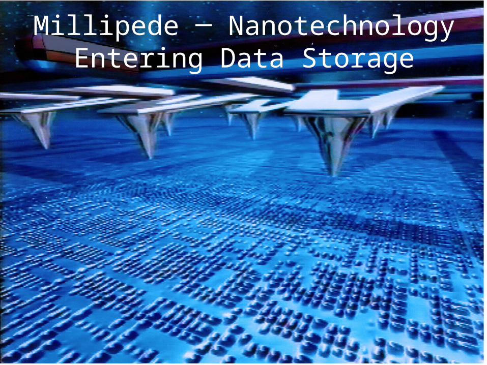
Millipede ─ Nanotechnology Entering Data Storage
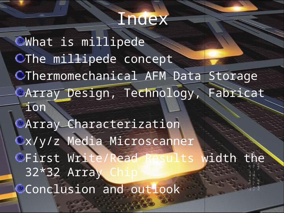
IndexWhat is millipede
The millipede concept
Thermomechanical AFM Data Storage
Array Design, Technology, Fabrication
Array Characterization
x/y/z Media Microscanner
First Write/Read Results width the 32*32 Array Chip
Conclusion and outlook
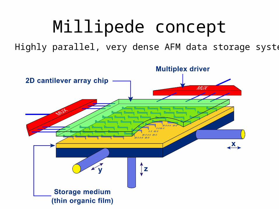
Millipede conceptHighly parallel, very dense AFM data storage system
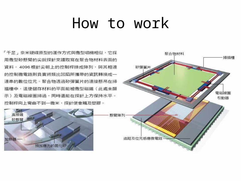
How to work
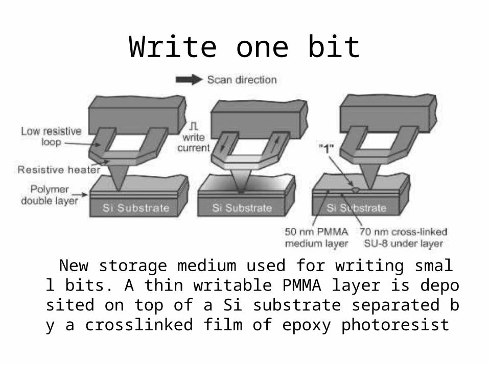
Write one bit
New storage medium used for writing small bits. A thin writable PMMA layer is deposited on top of a Si substrate separated by a crosslinked film of epoxy photoresist
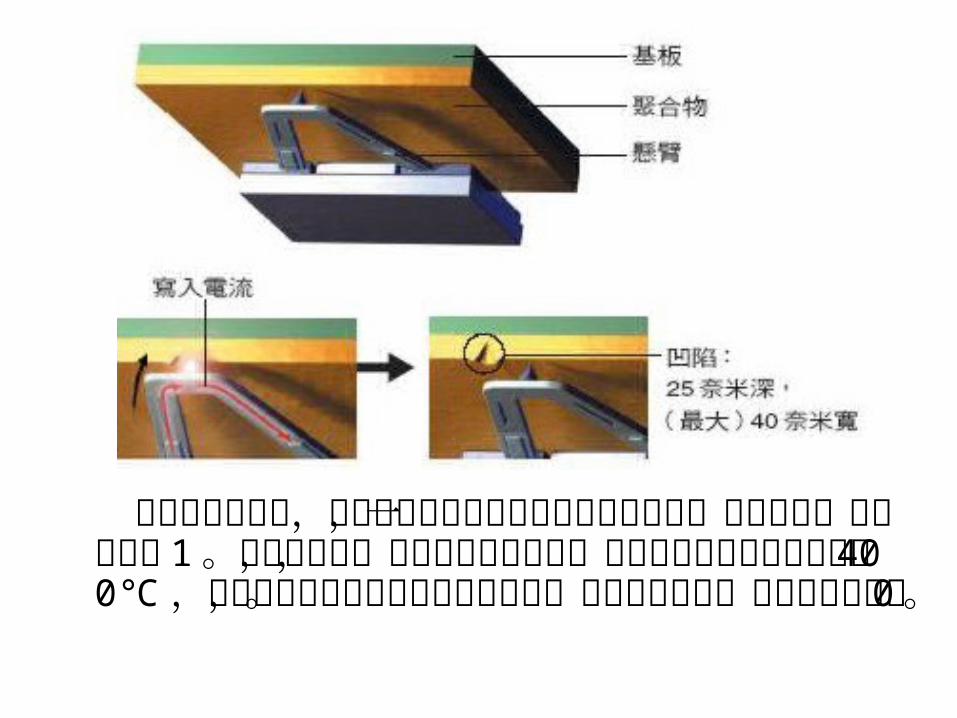
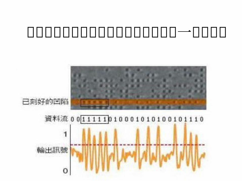
利用熱及機械力,針尖能製造出排成直線狀的圓錐凹陷,用來代表一連串的數字 1。要製造凹陷,電流必須流經懸臂,將其尾端的矽摻雜區加熱至400℃,以便讓預加應力的懸臂結構能彎曲,戳入聚合物中。沒有凹陷則代表 0。
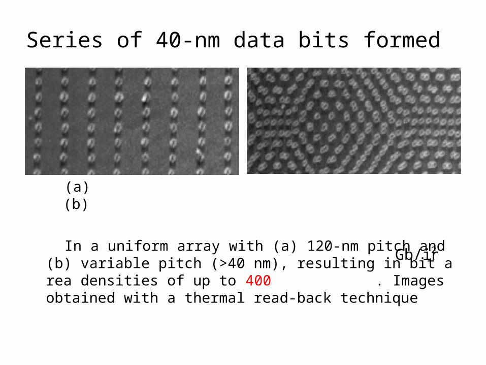
Series of 40-nm data bits formed
(a) (b)
In a uniform array with (a) 120-nm pitch and (b) variable pitch (>40 nm), resulting in bit area densities of up to 400 . Images obtained with a thermal read-back technique
2Gb/in
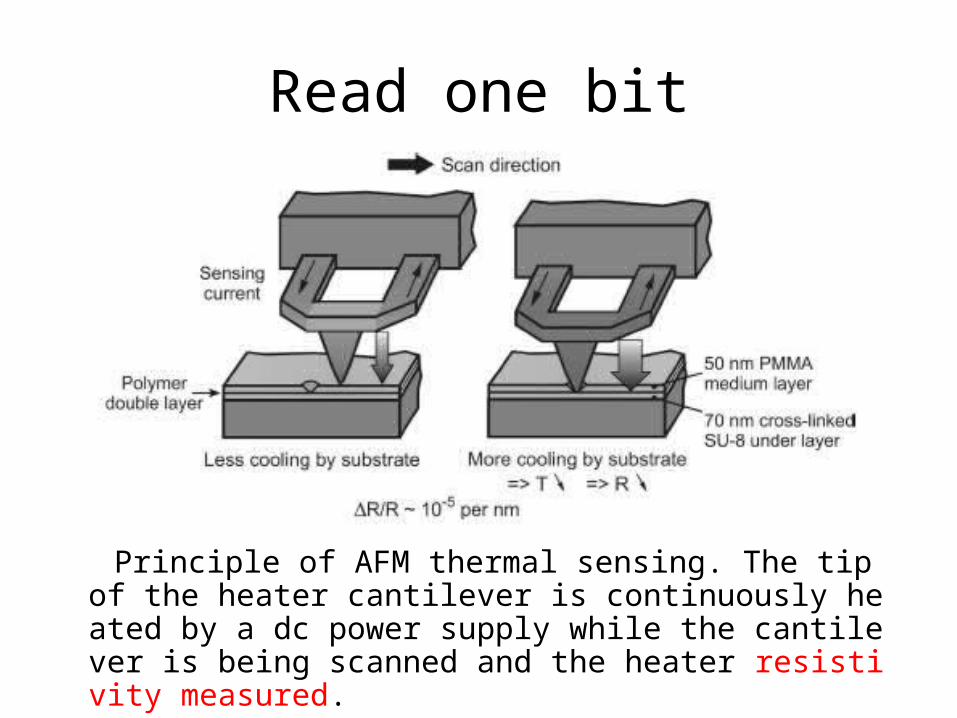
Read one bit
Principle of AFM thermal sensing. The tip of the heater cantilever is continuously heated by a dc power supply while the cantilever is being scanned and the heater resistivity measured.
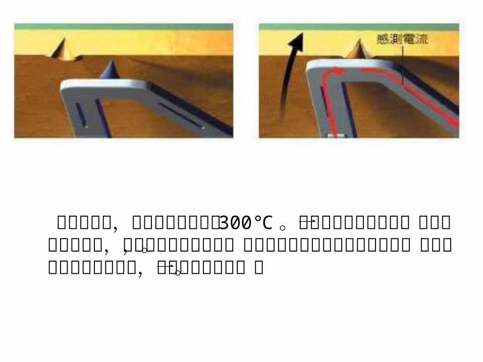
要讀取資料,先將針尖加熱至約 300℃。當掃描中的針尖遇到一個凹陷並落入其中,它會將熱傳遞給塑膠,針尖的溫度及電阻就會因此下降。不過電阻下降的幅度很小,約只有幾千分之一。
數位訊號處理器將這些輸出訊號轉換成一連串資料
Clear one bit
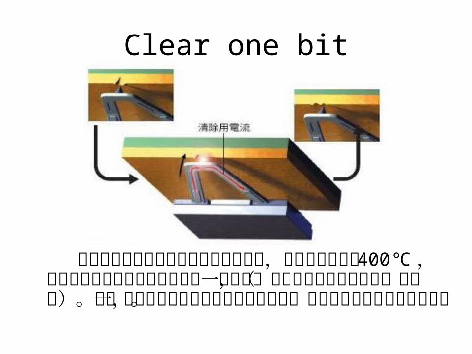
最新的千足原型機清除既存位元的方式,是將針尖加熱至 400℃,緊挨著先前刻出的凹陷再製造另一個凹陷,如此會將原來的坑填滿(見上圖)。另一種做法是將熾熱的針尖插入凹陷中,使塑膠彈回原本的平坦形狀。
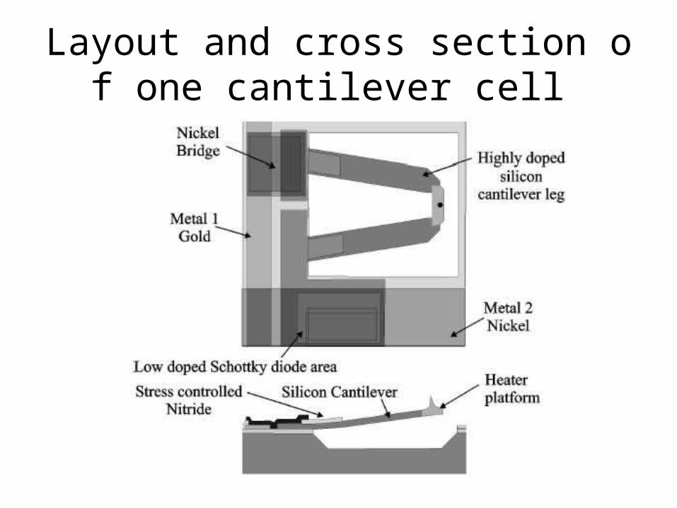
Layout and cross section of one cantilever cell
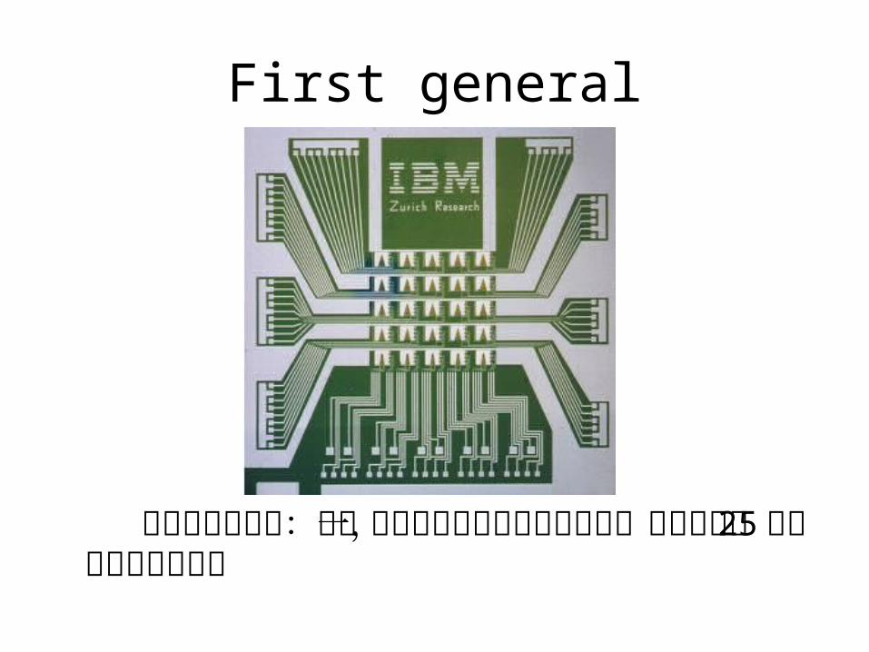
First general
原型晶片的演變:第一代的千足晶片邊長為五毫米,其中包含了 25根懸臂所組成的陣列
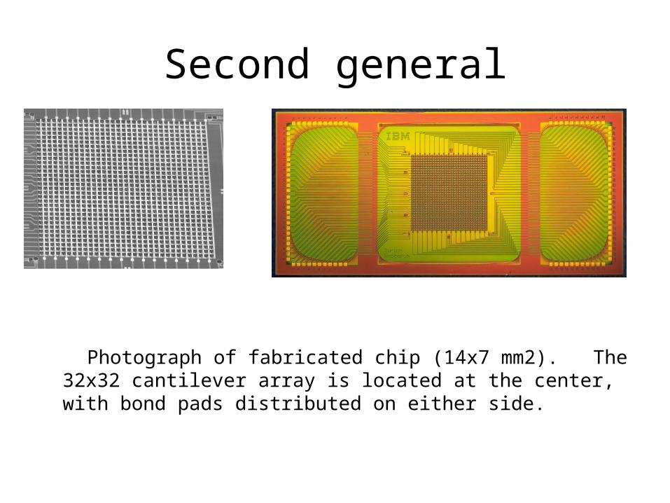
Second general
Photograph of fabricated chip (14x7 mm2). The 32x32 cantilever array is located at the center, with bond pads distributed on either side.
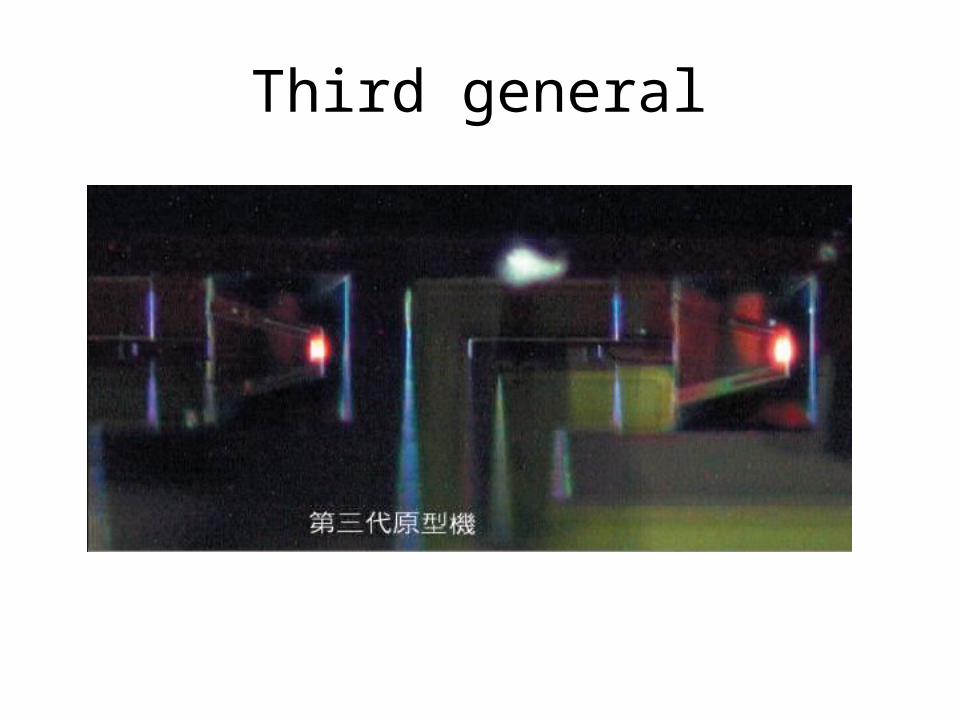
Third general
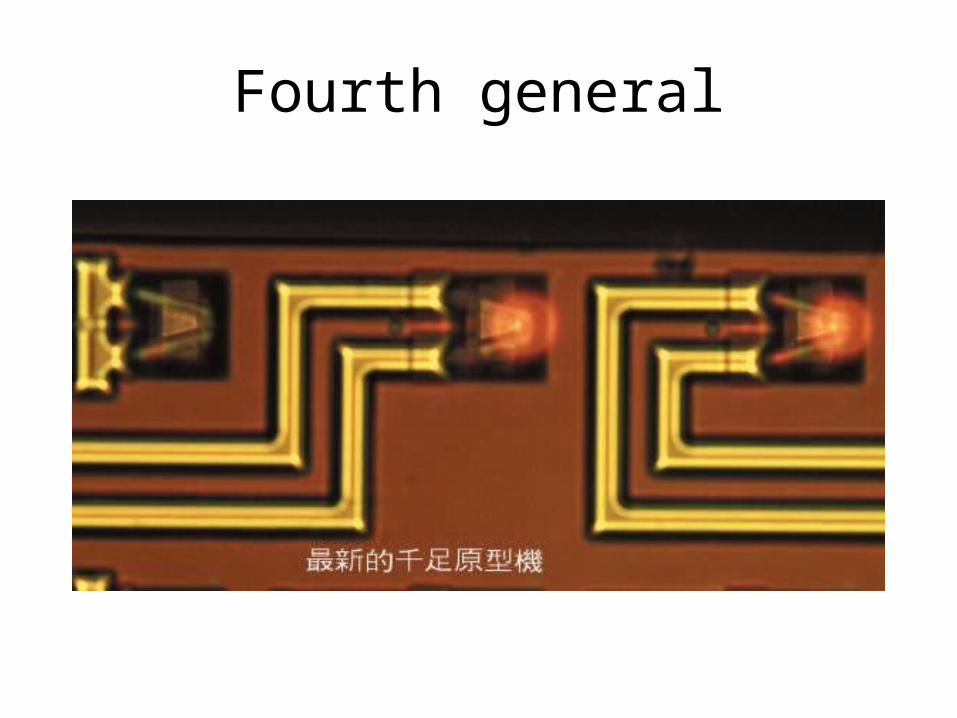
Fourth general
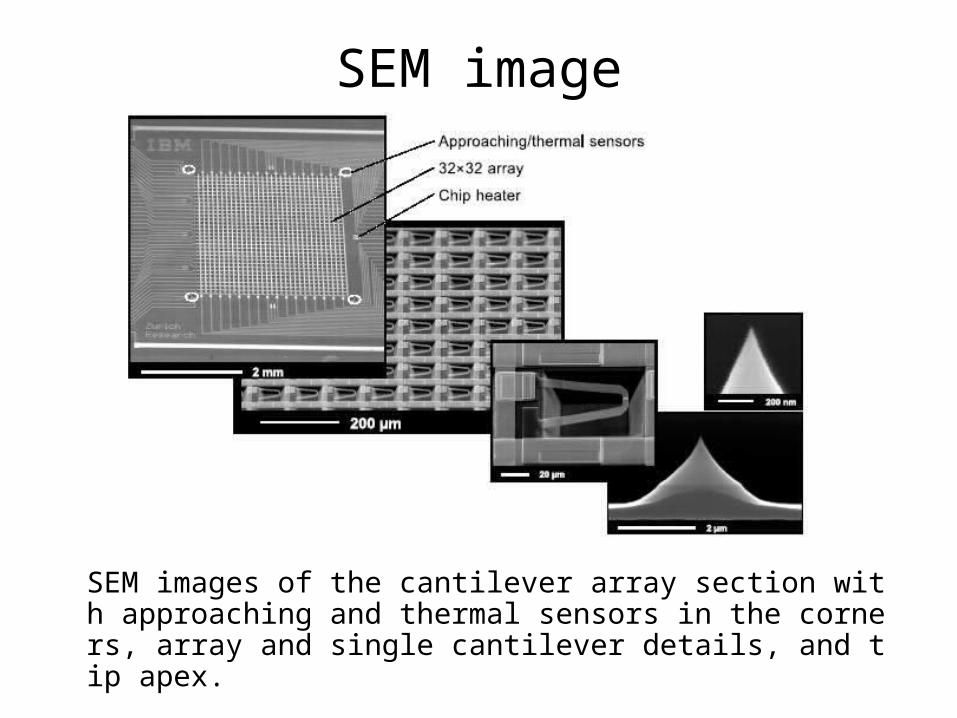
SEM images of the cantilever array section with approaching and thermal sensors in the corners, array and single cantilever details, and tip apex.
SEM image
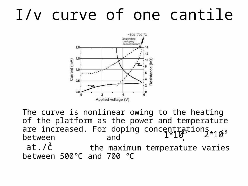
I/v curve of one cantilever
The curve is nonlinear owing to the heating of the platform as the power and temperature are increased. For doping concentrations between and ,
the maximum temperature varies between 500 ℃and 700 ℃
3at./cm
1710*1 1810*2
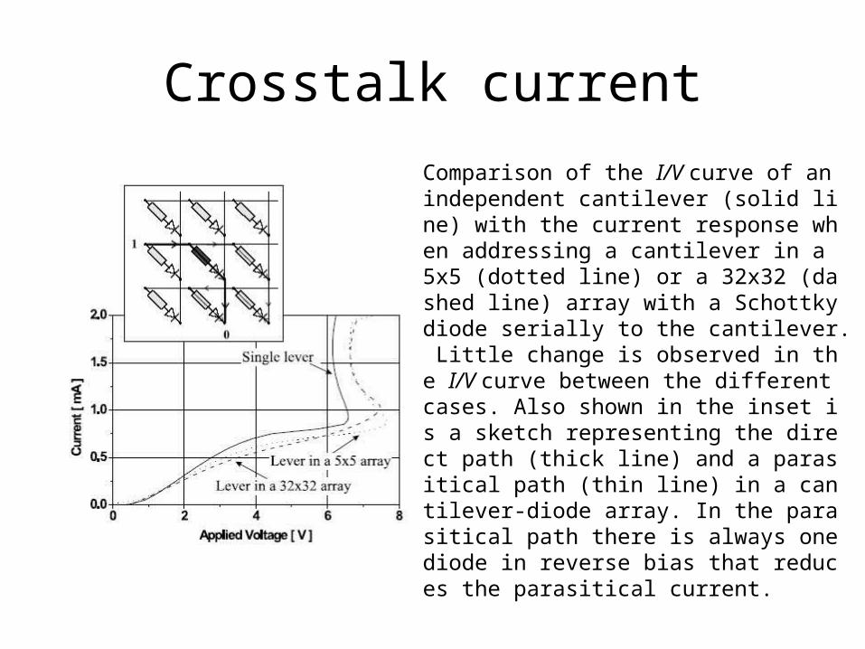
Crosstalk current
Comparison of the I/V curve of an independent cantilever (solid line) with the current response when addressing a cantilever in a 5x5 (dotted line) or a 32x32 (dashed line) array with a Schottky diode serially to the cantilever. Little change is observed in the I/V curve between the different cases. Also shown in the inset is a sketch representing the direct path (thick line) and a parasitical path (thin line) in a cantilever-diode array. In the parasitical path there is always one diode in reverse bias that reduces the parasitical current.
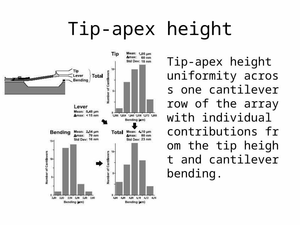
Tip-apex height
Tip-apex height uniformity across one cantilever row of the array with individual contributions from the tip height and cantilever bending.
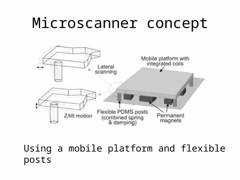
Microscanner concept
Using a mobile platform and flexible posts
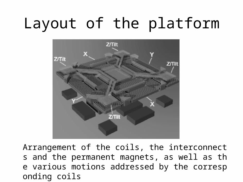
Layout of the platform
Arrangement of the coils, the interconnects and the permanent magnets, as well as the various motions addressed by the corresponding coils
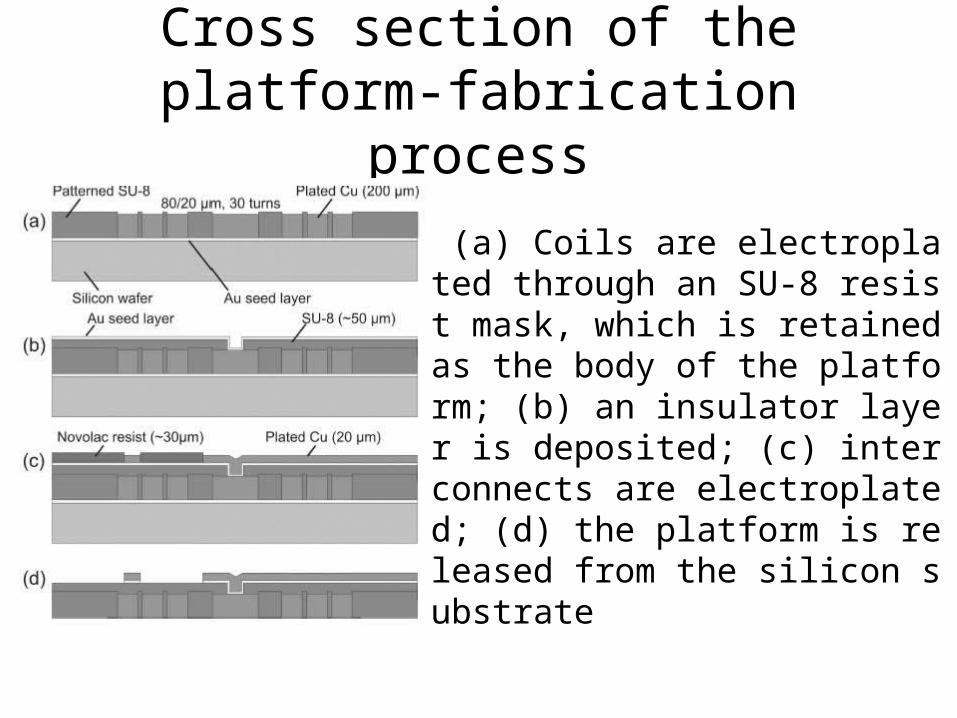
Cross section of the platform-fabrication process
(a) Coils are electroplated through an SU-8 resist mask, which is retained as the body of the platform; (b) an insulator layer is deposited; (c) interconnects are electroplated; (d) the platform is released from the silicon substrate
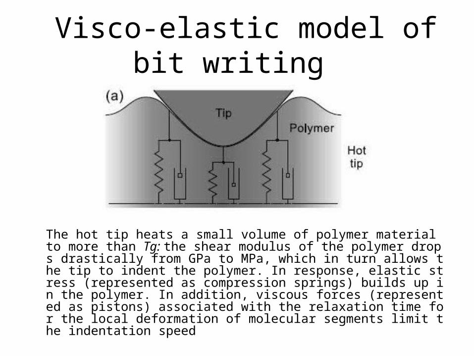
Visco-elastic model of bit writing
The hot tip heats a small volume of polymer material to more than Tg: the shear modulus of the polymer drops drastically from GPa to MPa, which in turn allows the tip to indent the polymer. In response, elastic stress (represented as compression springs) builds up in the polymer. In addition, viscous forces (represented as pistons) associated with the relaxation time for the local deformation of molecular segments limit the indentation speed
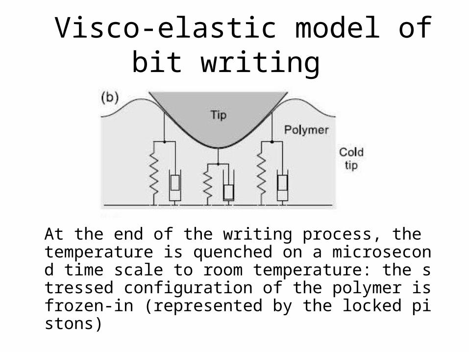
Visco-elastic model of bit writing
At the end of the writing process, the temperature is quenched on a microsecond time scale to room temperature: the stressed configuration of the polymer is frozen-in (represented by the locked pistons)
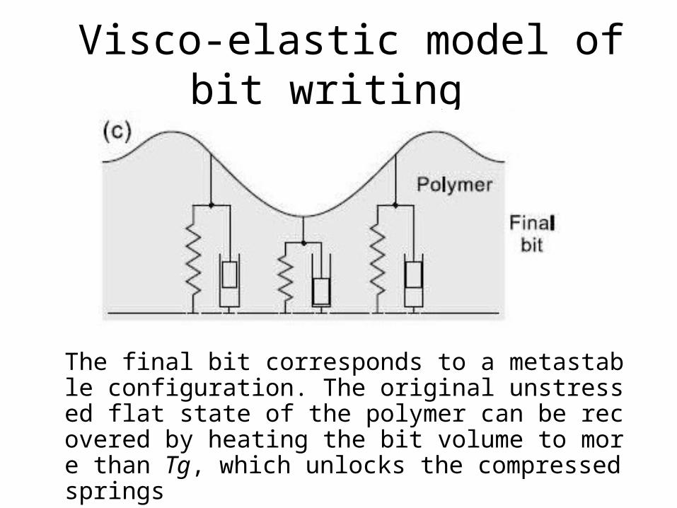
Visco-elastic model of bit writing
The final bit corresponds to a metastable configuration. The original unstressed flat state of the polymer can be recovered by heating the bit volume to more than Tg, which unlocks the compressed springs
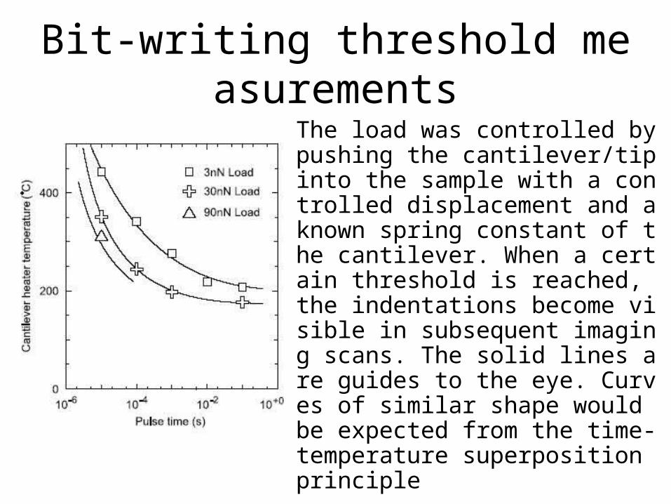
Bit-writing threshold measurements
The load was controlled by pushing the cantilever/tip into the sample with a controlled displacement and a known spring constant of the cantilever. When a certain threshold is reached, the indentations become visible in subsequent imaging scans. The solid lines are guides to the eye. Curves of similar shape would be expected from the time-temperature superposition principle
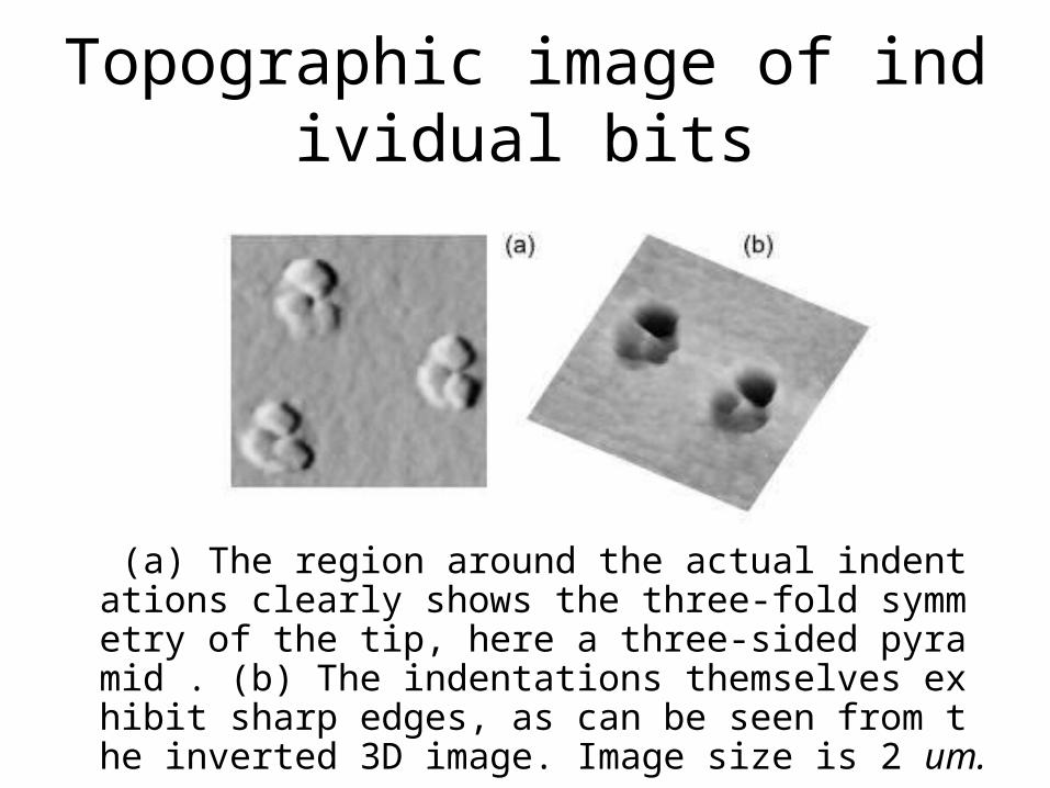
Topographic image of individual bits
(a) The region around the actual indentations clearly shows the three-fold symmetry of the tip, here a three-sided pyramid . (b) The indentations themselves exhibit sharp edges, as can be seen from the inverted 3D image. Image size is 2 um.
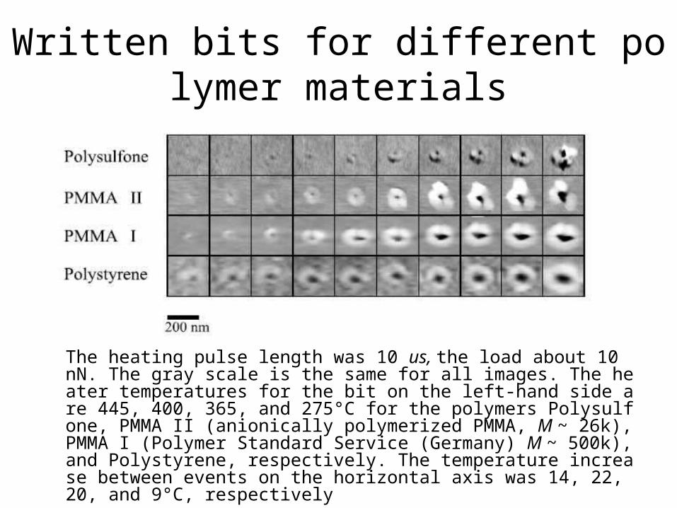
Written bits for different polymer materials
The heating pulse length was 10 us, the load about 10 nN. The gray scale is the same for all images. The heater temperatures for the bit on the left-hand side are 445, 400, 365, and 275°C for the polymers Polysulfone, PMMA II (anionically polymerized PMMA, M ~ 26k), PMMA I (Polymer Standard Service (Germany) M ~ 500k), and Polystyrene, respectively. The temperature increase between events on the horizontal axis was 14, 22, 20, and 9°C, respectively
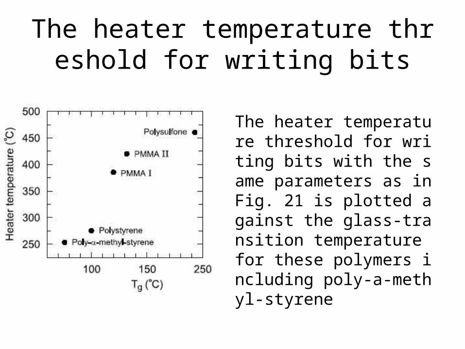
The heater temperature threshold for writing bits
The heater temperature threshold for writing bits with the same parameters as in Fig. 21 is plotted against the glass-transition temperature for these polymers including poly-a-methyl-styrene
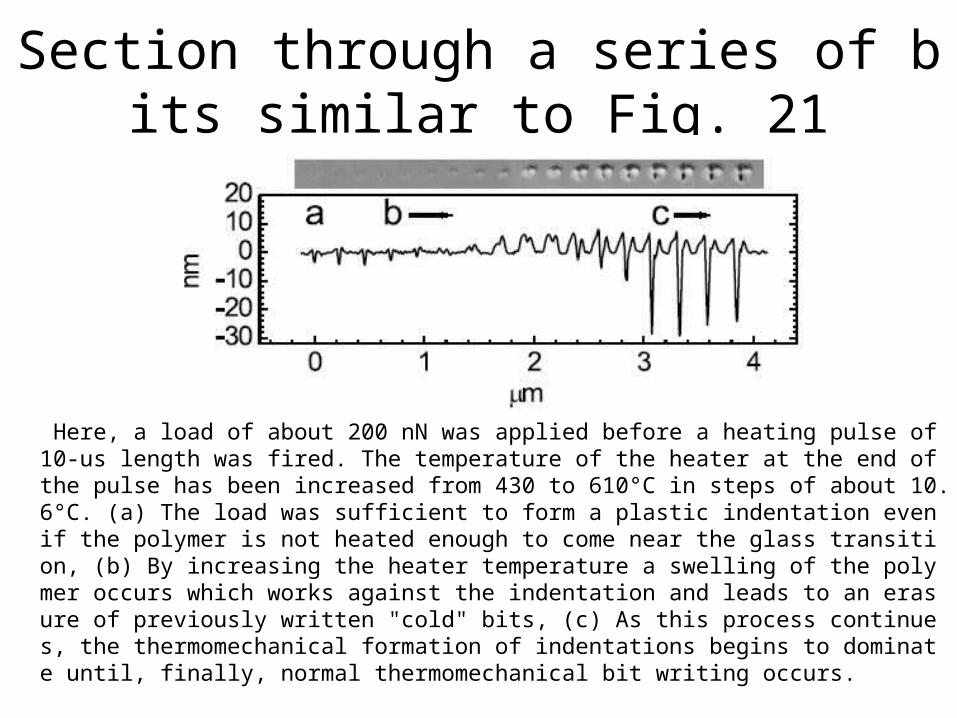
Section through a series of bits similar to Fig. 21
Here, a load of about 200 nN was applied before a heating pulse of 10-us length was fired. The temperature of the heater at the end of the pulse has been increased from 430 to 610°C in steps of about 10.6°C. (a) The load was sufficient to form a plastic indentation even if the polymer is not heated enough to come near the glass transition, (b) By increasing the heater temperature a swelling of the polymer occurs which works against the indentation and leads to an erasure of previously written "cold" bits, (c) As this process continues, the thermomechanical formation of indentations begins to dominate until, finally, normal thermomechanical bit writing occurs.
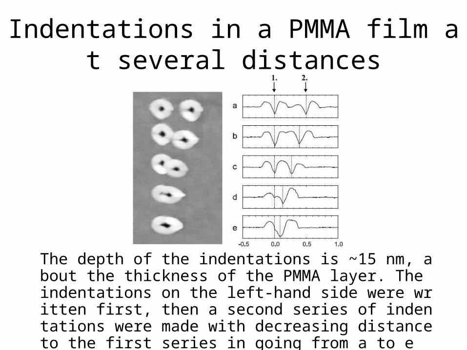
Indentations in a PMMA film at several distances
The depth of the indentations is ~15 nm, about the thickness of the PMMA layer. The indentations on the left-hand side were written first, then a second series of indentations were made with decreasing distance to the first series in going from a to e
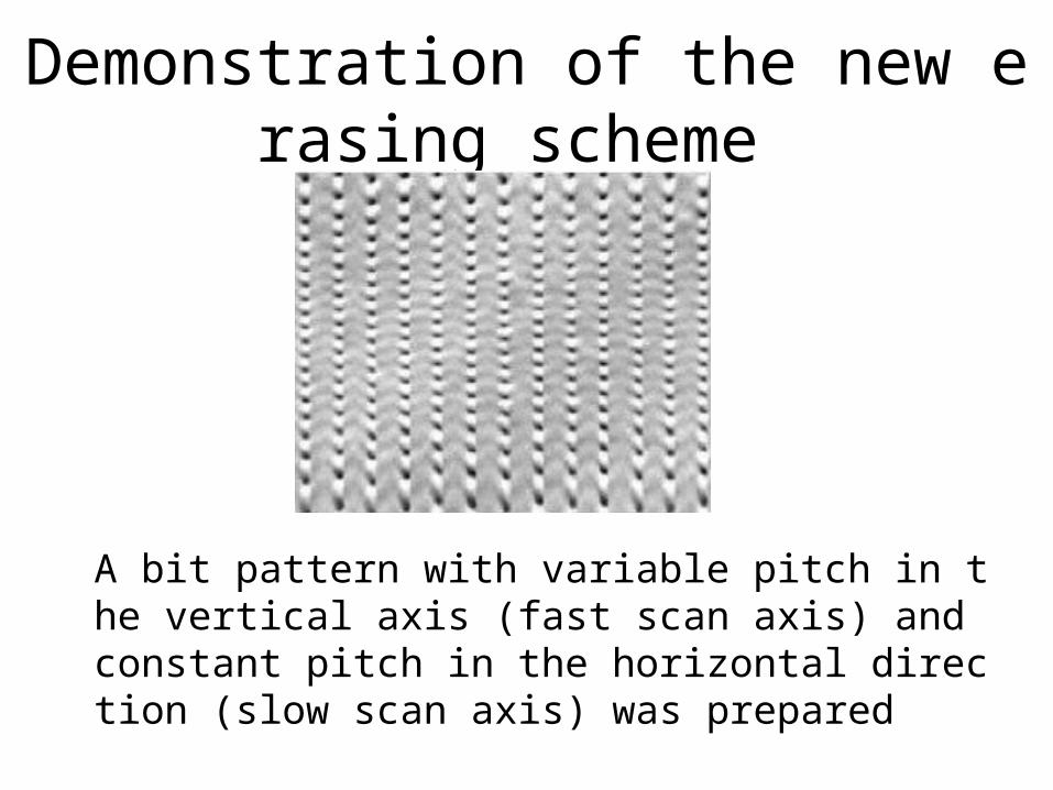
Demonstration of the new erasing scheme
A bit pattern with variable pitch in the vertical axis (fast scan axis) and constant pitch in the horizontal direction (slow scan axis) was prepared

Demonstration of the new erasing scheme
Then two of the lines were erased by decreasing the pitch in the vertical direction by a factor of three, showing that the erasing scheme works for individual lines. One can also erase entire fields of bits without destroying bits at the edges of the fields
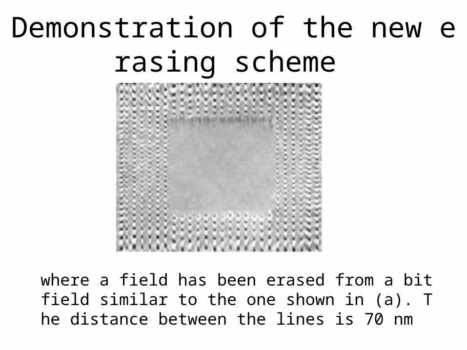
Demonstration of the new erasing scheme
where a field has been erased from a bit field similar to the one shown in (a). The distance between the lines is 70 nm
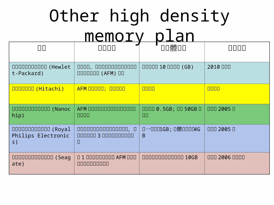
Other high density memory plan公司 元件技術 記憶體容量 上市時間
美國加州帕洛亞托的惠普(Hewlett-Packard)
拇指大小、以電子束將資料讀寫入儲存區的原子力顯微鏡 (AFM) 元件
開始至少有 10 億位元組(GB)
2010 年之前
日本東京的日立 (Hitachi) AFM 為主的元件;細節未公開
尚未透露 尚未公佈
美國加州奧克蘭的奈米晶片 (Nanochip)
AFM 針尖加裝懸臂陣列用來將資料儲存在晶片中
最初只有 0.5GB; 但有 50GB 的潛力
預計在 2005 年
荷蘭愛因荷芬的皇家飛利浦 (Royal Philips Electronics)
與可重複寫入光碟相類似的光學系統,採用藍光雷射在 3 公分寬的碟面上讀寫資料
每一面可達 1GB;整體可能達到 4GB
預計在 2005 年
美國加州斯科次谷的希捷科技 (Seagate)
在 1 公分寬的晶片上應用AFM或其他方法的可重複讀寫系統
在可攜帶式裝置的晶片上可達 10GB
預計在 2006 年或之後
A number of issues to be addressed
Overall system reliability, including bit stability, tip and medium wear, erasing/ rewriting.
CMOS integration.
Optimization of write/read multiplexing scheme.
Array-chip tracking.
Data rate versus power consumption tradeoffs.