mixed-signal control processor with arm cortex …...trol processor with arm cortex-m4 hardware...
TRANSCRIPT
Mixed-Signal Control Processorwith ARM Cortex-M4 and 16-Bit ADCs
ADSP-CM402F/CM403F/CM407F/CM408F/CM409F
Rev. A Document FeedbackInformation furnished by Analog Devices is believed to be accurate and reliable.However, no responsibility is assumed by Analog Devices for its use, nor for anyinfringements of patents or other rights of third parties that may result from its use.Specifications subject to change without notice. No license is granted by implicationor otherwise under any patent or patent rights of Analog Devices. Trademarks andregistered trademarks are the property of their respective owners.
One Technology Way, P.O. Box 9106, Norwood, MA 02062-9106 U.S.A.Tel: 781.329.4700 ©2015 Analog Devices, Inc. All rights reserved.Technical Support www.analog.com
SYSTEM FEATURESUp to 240 MHz ARM Cortex-M4 with floating-point unit 24-channel analog front end (AFE) with 16-bit ADCs128K Byte to 384K Byte zero-wait-state L1 SRAM with
16K Byte L1 cacheUp to 2M Byte flash memorySingle 3.3 V power supplyPackage Options:
176-lead (24 mm × 24 mm) LQFP package120-lead (14 mm × 14 mm) LQFP package212-ball (19 mm × 19 mm) BGA package
Static memory controller (SMC) with asynchronous memory interface that supports 8-bit and 16-bit memories
Enhanced PWM unitsFour 3rd/4th order SINC filter pairs for glueless connection of
sigma-delta modulatorsHardware-based harmonic analysis engine10/100 Ethernet MAC with IEEE 1588v2 support
Full Speed USB on-the-go (OTG)Two CAN (controller area network) 2.0B interfacesThree UART portsTwo serial peripheral interface (SPI-compatible) portsThree/four synchronous serial portsEight 32-bit GP timers, three capture timing unitsFour encoder interfaces, 2 with frequency divisionOne TWI unit, fully compatible with I2C bus standardLightweight security
ANALOG FRONT ENDTwo 16-bit SAR ADCs with up to 24 multiplexed inputs,
supporting dual simultaneous conversion in 380 ns (16-bit, no missing codes)
ADC controller (ADCC) and DAC controller (DACC)Two 12-bit DACsTwo 2.5 V precision voltage reference outputs(For details, see ADC/DAC Specifications on Page 68)
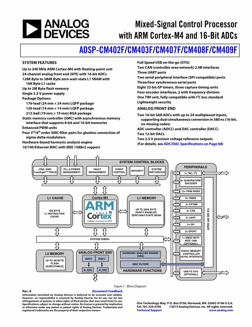
Figure 1. Block Diagram
UP TO 2M BYTEFLASH
(EXECUTABLE)
L1 CACHE
16K BYTEL1 INSTRUCTION
CACHE
SYSTEM CONTROL BLOCKS
PERIPHERALS
HARDWARE FUNCTIONS
L3 MEMORY
SYSTEM FABRIC 1× EMAC WITHIEEE 1588
(OPTIONAL)
2x SPORT
2× CAN
STATIC MEMORYCONTROLLER
ASYNC INTERFACE
2× SPI
4× QUADRATUREENCODER
8× TIMER
12× PWM PAIRS
1× TWI / I2C
USB FS OTG(OPTIONAL)
L1 MEMORY
UP TO 384K BYTE PARITY-ENABLED
ZERO-WAIT-STATE SRAM
JTAG, SWD, CoreSight™ TRACE
EVENTCONTROL
SYSTEMWATCHDOGS
PLL & POWERMANAGEMENT
FAULTMANAGEMENT
3× UART
ADCC DACC
HARMONIC ANALYSIS ENGINE(HAE)
ANALOG FRONT END
GPI
O (4
0 O
R 9
1)
2× ADC 2× DAC
SINC FILTERS
SECURITY
Cortex-M4
3× CPTMR
Rev. A | Page 2 of 124 | November 2015
ADSP-CM402F/CM403F/CM407F/CM408F/CM409FTABLE OF CONTENTSGeneral Description . . . . . . . . . . . . . . . . . . . . . . . . . . . . . . . . . . . . . . . . . . . . . . . . . 3
Analog Front End . . . . . . . . . . . . . . . . . . . . . . . . . . . . . . . . . . . . . . . . . . . . . . . . . 4ARM Cortex-M4 Core . . . . . . . . . . . . . . . . . . . . . . . . . . . . . . . . . . . . . . . . . . . 7EmbeddedICE . . . . . . . . . . . . . . . . . . . . . . . . . . . . . . . . . . . . . . . . . . . . . . . . . . . . . . 7Processor Infrastructure . . . . . . . . . . . . . . . . . . . . . . . . . . . . . . . . . . . . . . . . . 8Memory Architecture . . . . . . . . . . . . . . . . . . . . . . . . . . . . . . . . . . . . . . . . . . . . 8System Acceleration . . . . . . . . . . . . . . . . . . . . . . . . . . . . . . . . . . . . . . . . . . . . 10Security Features . . . . . . . . . . . . . . . . . . . . . . . . . . . . . . . . . . . . . . . . . . . . . . . . 10Processor Reliability Features . . . . . . . . . . . . . . . . . . . . . . . . . . . . . . . . . 11Additional Processor Peripherals . . . . . . . . . . . . . . . . . . . . . . . . . . . . 11Clock and Power Management . . . . . . . . . . . . . . . . . . . . . . . . . . . . . . . 14System Debug Unit (SDU) . . . . . . . . . . . . . . . . . . . . . . . . . . . . . . . . . . . . 16Development Tools . . . . . . . . . . . . . . . . . . . . . . . . . . . . . . . . . . . . . . . . . . . . . 17Additional Information . . . . . . . . . . . . . . . . . . . . . . . . . . . . . . . . . . . . . . . . 17Related Signal Chains . . . . . . . . . . . . . . . . . . . . . . . . . . . . . . . . . . . . . . . . . . 17Security Features Disclaimer . . . . . . . . . . . . . . . . . . . . . . . . . . . . . . . . . . 17
ADSP-CM40xF Detailed Signal Descriptions . . . . . . . . . . . . . . . . 18ADSP-CM402F/ADSP-CM403F 120-Lead LQFP
Signal Descriptions . . . . . . . . . . . . . . . . . . . . . . . . . . . . . . . . . . . . . . . . . . . . . 22ADSP-CM402F/ADSP-CM403F GPIO Multiplexing
for 120-Lead LQFP . . . . . . . . . . . . . . . . . . . . . . . . . . . . . . . . . . . . . . . . . . . . . . 27ADSP-CM407F/ADSP-CM408F 176-Lead LQFP
Signal Descriptions . . . . . . . . . . . . . . . . . . . . . . . . . . . . . . . . . . . . . . . . . . . . . 29ADSP-CM407F/ADSP-CM408F GPIO Multiplexing
for 176-Lead LQFP . . . . . . . . . . . . . . . . . . . . . . . . . . . . . . . . . . . . . . . . . . . . . . 37
ADSP-CM409F 212-Ball BGA Signal Descriptions . . . . . . . . . 40ADSP-CM409F GPIO Multiplexing for 212-Ball BGA .. . . . 48ADSP-CM40xF Designer Quick Reference . . . . . . . . . . . . . . . . . . . 51Specifications . . . . . . . . . . . . . . . . . . . . . . . . . . . . . . . . . . . . . . . . . . . . . . . . . . . . . . . . 64
Operating Conditions . . . . . . . . . . . . . . . . . . . . . . . . . . . . . . . . . . . . . . . . . . . 64Electrical Characteristics . . . . . . . . . . . . . . . . . . . . . . . . . . . . . . . . . . . . . . . 66ADC/DAC Specifications . . . . . . . . . . . . . . . . . . . . . . . . . . . . . . . . . . . . . . 68Flash Specifications . . . . . . . . . . . . . . . . . . . . . . . . . . . . . . . . . . . . . . . . . . . . . . 74Absolute Maximum Ratings . . . . . . . . . . . . . . . . . . . . . . . . . . . . . . . . . . . 75ESD Sensitivity . . . . . . . . . . . . . . . . . . . . . . . . . . . . . . . . . . . . . . . . . . . . . . . . . . . 75Package Information . . . . . . . . . . . . . . . . . . . . . . . . . . . . . . . . . . . . . . . . . . . . 75Timing Specifications . . . . . . . . . . . . . . . . . . . . . . . . . . . . . . . . . . . . . . . . . . . 76Processor Test Conditions . . . . . . . . . . . . . . . . . . . . . . . . . . . . . . . . . . . 107Output Drive Currents . . . . . . . . . . . . . . . . . . . . . . . . . . . . . . . . . . . . . . . 107Environmental Conditions . . . . . . . . . . . . . . . . . . . . . . . . . . . . . . . . . . 108
ADSP-CM402F/ADSP-CM403F 120-Lead LQFP Lead Assignments . . . . . . . . . . . . . . . . . . . . . . . . . . . . . . . . . . . . . . . . . . . . . 110
ADSP-CM407F/ADSP-CM408F 176-Lead LQFP Lead Assignments . . . . . . . . . . . . . . . . . . . . . . . . . . . . . . . . . . . . . . . . . . . . . 113
ADSP-CM409F 212-Ball BGA Ball Assignments . . . . . . . . . . 117Outline Dimensions . . . . . . . . . . . . . . . . . . . . . . . . . . . . . . . . . . . . . . . . . . . . . . 121
Ordering Guide . . . . . . . . . . . . . . . . . . . . . . . . . . . . . . . . . . . . . . . . . . . . . . . . 124
REVISION HISTORY11/15—Rev. 0 to Rev. A
Changes to Ordering Guide . . . . . . . . . . . . . . . . . . . . . . . . . . . . . . . . . . . . . 124
Change to equation in Serial Ports . . . . . . . . . . . . . . . . . . . . . . . . . . . . . 83Change to equation in Serial Peripheral Interface (SPI) Port—Master Timing . . . . . . . . . . . . . . . . . . . . . . . . . . . . . . . . . . . . . . . . . . . . . . . . . . . . . . 89
Rev. A | Page 3 of 124 | November 2015
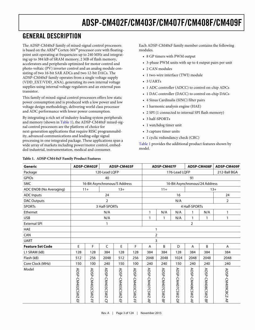
ADSP-CM402F/CM403F/CM407F/CM408F/CM409FGENERAL DESCRIPTIONThe ADSP-CM40xF family of mixed-signal control processors is based on the ARM® Cortex-M4TM processor core with floating-point unit operating at frequencies up to 240 MHz and integrat-ing up to 384 kB of SRAM memory, 2 MB of flash memory, accelerators and peripherals optimized for motor control and photo-voltaic (PV) inverter control and an analog module con-sisting of two 16-bit SAR ADCs and two 12-bit DACs. The ADSP-CM40xF family operates from a single voltage supply (VDD_EXT/VDD_ANA), generating its own internal voltage supplies using internal voltage regulators and an external pass transistor.This family of mixed-signal control processors offers low static power consumption and is produced with a low power and low voltage design methodology, delivering world class processor and ADC performance with lower power consumption. By integrating a rich set of industry-leading system peripherals and memory (shown in Table 1), the ADSP-CM40xF mixed-sig-nal control processors are the platform of choice for next-generation applications that require RISC programmabil-ity, advanced communications and leading-edge signal processing in one integrated package. These applications span a wide array of markets including power/motor control, embed-ded industrial, instrumentation, medical and consumer.
Each ADSP-CM40xF family member contains the following modules.
• 8 GP timers with PWM output• 3-phase PWM units with up to 4 output pairs per unit• 2 CAN modules• 1 two-wire interface (TWI) module• 3 UARTs• 1 ADC controller (ADCC) to control on-chip ADCs• 1 DAC controller (DACC) to control on-chip DACs• 4 Sinus Cardinalis (SINC) filter pairs• 1 harmonic analysis engine (HAE)• 2 SPI (1 connected to internal SPI flash memory)• 3 half-SPORTs• 1 watchdog timer unit• 3 capture timer units• 1 cyclic redundancy check (CRC)
Table 1 provides the additional product features shown by model.
Table 1. ADSP-CM4 0xF Family Product Features
Generic ADSP-CM402F ADSP-CM403F ADSP-CM407F ADSP-CM408F ADSP-CM409FPackage 120-Lead LQFP 176-Lead LQFP 212-Ball BGA
GPIOs 40 91
SMC 16-Bit Asynchronous/5 Address 16-Bit Asynchronous/24 Address
ADC ENOB (No Averaging) 11+ 13+ 11+ 13+
ADC Inputs 24 16 24
DAC Outputs 2 N/A 2
SPORTs 3 Half-SPORTs 4 Half-SPORTs
Ethernet N/A 1 N/A N/A 1 N/A 1
USB N/A 1 1 N/A 1 1 1
External SPI 1 2
HAE 1
CAN 2
UART 3
Feature Set Code E F C E F A B D A B A
L1 SRAM (kB) 128 128 384 128 128 384 384 128 384 384 384
Flash (kB) 512 256 2048 512 256 2048 2048 1024 2048 2048 2048
Core Clock (MHz) 150 100 240 150 100 240 240 150 240 240 240
Model
AD
SP-CM402CSW
Z-EF
AD
SP-CM402CSW
Z-FF
AD
SP-CM403CSW
Z-CF
AD
SP-CM403CSW
Z-EF
AD
SP-CM403CSW
Z-FF
AD
SP-CM407CSW
Z-AF
AD
SP-CM407CSW
Z-BF
AD
SP-CM407CSW
Z-DF
AD
SP-CM408CSW
Z-AF
AD
SP-CM408CSW
Z-BF
AD
SP-CM409CBCZ-A
F
Rev. A | Page 4 of 124 | November 2015
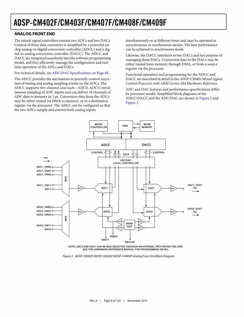
ADSP-CM402F/CM403F/CM407F/CM408F/CM409FANALOG FRONT ENDThe mixed-signal controllers contain two ADCs and two DACs. Control of these data converters is simplified by a powerful on-chip analog-to-digital conversion controller (ADCC) and a dig-ital-to-analog conversion controller (DACC). The ADCC and DACC are integrated seamlessly into the software programming model, and they efficiently manage the configuration and real-time operation of the ADCs and DACs. For technical details, see ADC/DAC Specifications on Page 68.The ADCC provides the mechanism to precisely control execu-tion of timing and analog sampling events on the ADCs. The ADCC supports two-channel (one each—ADC0, ADC1) simul-taneous sampling of ADC inputs and can deliver 16 channels of ADC data to memory in 3 μs. Conversion data from the ADCs may be either routed via DMA to memory, or to a destination register via the processor. The ADCC can be configured so that the two ADCs sample and convert both analog inputs
simultaneously or at different times and may be operated in asynchronous or synchronous modes. The best performance can be achieved in synchronous mode.Likewise, the DACC interfaces to two DACs and has purpose of managing those DACs. Conversion data to the DACs may be either routed from memory through DMA, or from a source register via the processor.Functional operation and programming for the ADCC and DACC are described in detail in the ADSP-CM40x Mixed-Signal Control Processor with ARM Cortex-M4 Hardware Reference.ADC and DAC features and performance specifications differ by processor model. Simplified block diagrams of the ADCC/DACC and the ADC/DAC are shown in Figure 2 and Figure 3.
Figure 2. ADSP-CM402F/ADSP-CM403F/ADSP-CM409F Analog Front End Block Diagram
DAC1
DAC0ADC0
ADC1_VIN00
.
.
.
ADC1_VIN01ADC1_VIN02
ADC1_VIN11DAC1
ADC0_VIN00
.
.
.
ADC0_VIN01ADC0_VIN02
ADC0_VIN11DAC0
MU
X M
UX
ADCC DACC
CONTROL CONTROL
MICROCONTROLLER DMA SRAM
MEMORY
DATA
VREF1VREF0
REFCAP
BUF
BUF
BUF
BUF
BUFBUF
DAC1_VOUT
DAC0_VOUT
~
~
~
ADC1
BUFBUF
BANDGAP
ADC/DACLOCAL CONTROLLER
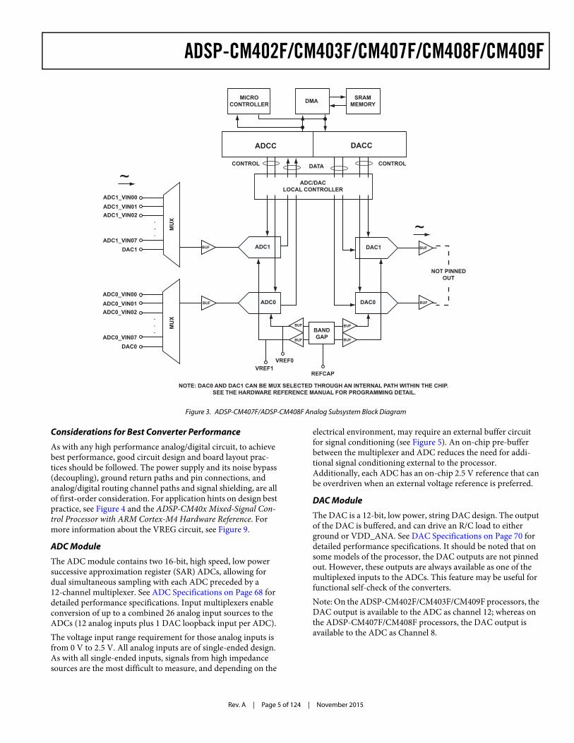
NOTE: DAC0 AND DAC1 CAN BE MUX SELECTED THROUGH AN INTERNAL PATH WITHIN THE CHIP. SEE THE HARDWARE REFERENCE MANUAL FOR PROGRAMMING DETAIL.
Rev. A | Page 5 of 124 | November 2015
ADSP-CM402F/CM403F/CM407F/CM408F/CM409F
Considerations for Best Converter Performance
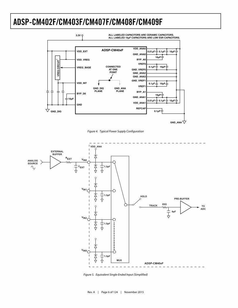
As with any high performance analog/digital circuit, to achieve best performance, good circuit design and board layout prac-tices should be followed. The power supply and its noise bypass (decoupling), ground return paths and pin connections, and analog/digital routing channel paths and signal shielding, are all of first-order consideration. For application hints on design best practice, see Figure 4 and the ADSP-CM40x Mixed-Signal Con-trol Processor with ARM Cortex-M4 Hardware Reference. For more information about the VREG circuit, see Figure 9.
ADC Module
The ADC module contains two 16-bit, high speed, low power successive approximation register (SAR) ADCs, allowing for dual simultaneous sampling with each ADC preceded by a 12-channel multiplexer. See ADC Specifications on Page 68 for detailed performance specifications. Input multiplexers enable conversion of up to a combined 26 analog input sources to the ADCs (12 analog inputs plus 1 DAC loopback input per ADC). The voltage input range requirement for those analog inputs is from 0 V to 2.5 V. All analog inputs are of single-ended design. As with all single-ended inputs, signals from high impedance sources are the most difficult to measure, and depending on the
electrical environment, may require an external buffer circuit for signal conditioning (see Figure 5). An on-chip pre-buffer between the multiplexer and ADC reduces the need for addi-tional signal conditioning external to the processor. Additionally, each ADC has an on-chip 2.5 V reference that can be overdriven when an external voltage reference is preferred.
DAC Module
The DAC is a 12-bit, low power, string DAC design. The output of the DAC is buffered, and can drive an R/C load to either ground or VDD_ANA. See DAC Specifications on Page 70 for detailed performance specifications. It should be noted that on some models of the processor, the DAC outputs are not pinned out. However, these outputs are always available as one of the multiplexed inputs to the ADCs. This feature may be useful for functional self-check of the converters.Note: On the ADSP-CM402F/CM403F/CM409F processors, the DAC output is available to the ADC as channel 12; whereas on the ADSP-CM407F/CM408F processors, the DAC output is available to the ADC as Channel 8.
Figure 3. ADSP-CM407F/ADSP-CM408F Analog Subsystem Block Diagram
DAC1
DAC0
ADC1
ADC0
ADC1_VIN00
.
.
.
ADC1_VIN01ADC1_VIN02
ADC1_VIN07DAC1
ADC0_VIN00
.
.
.
ADC0_VIN01ADC0_VIN02
ADC0_VIN07DAC0
MU
XM
UX
ADCC DACC
CONTROL CONTROL
MICROCONTROLLER DMA SRAM
MEMORY
DATA
VREF1VREF0
REFCAP
BUF
BUF
BUF
BUF
BUFBUF
~
~
NOT PINNEDOUT
BUFBUF
BANDGAP
ADC/DACLOCAL CONTROLLER
NOTE: DAC0 AND DAC1 CAN BE MUX SELECTED THROUGH AN INTERNAL PATH WITHIN THE CHIP. SEE THE HARDWARE REFERENCE MANUAL FOR PROGRAMMING DETAIL.
Rev. A | Page 6 of 124 | November 2015
ADSP-CM402F/CM403F/CM407F/CM408F/CM409F
Figure 4. Typical Power Supply Configuration
Figure 5. Equivalent Single-Ended Input (Simplified)
VDD_EXT
VDD_VREG
VDD_INT
BYP_D0
GND
VDD_ANA0
GND_ANA0
BYP_A0
VREF0
GND_VREF0
REFCAP
GND_VREF1
VREF1
BYP_A1
GND_ANA1
VDD_ANA1
VR
EG
CIR
CU
IT1
GND_ANA
3.3V
CONNECTEDAT ONEPOINT
GND_DIGPLANE
GND_ANAPLANE
GND_DIG
GND_ANA2
GND_ANA3
VREG_BASE
ADSP-CM40xF 0.01μF 0.1μF 10μF
10μF
0.1μF 10μF
0.1μF 10μF
0.01μF 0.1μF 10μF
10μF
0.1μF
10μF
ALL LABELED CAPACITORS ARE CERAMIC CAPACITORS.ALL LABELED 10μF CAPACITORS ARE LOW ESR CAPACITORS.
ANALOGSOURCE
VIN0
VDD_ANA
EXTERNALBUFFER
CEXT
REXT
ADSP-CM40xF
HOLD
TOADC
TRACK
9pF
85
VIN1
VIN2
VINX
1.5pF
MUX
PRE-BUFFER1.5pF
1.5pF
1.5pF
Rev. A | Page 7 of 124 | November 2015
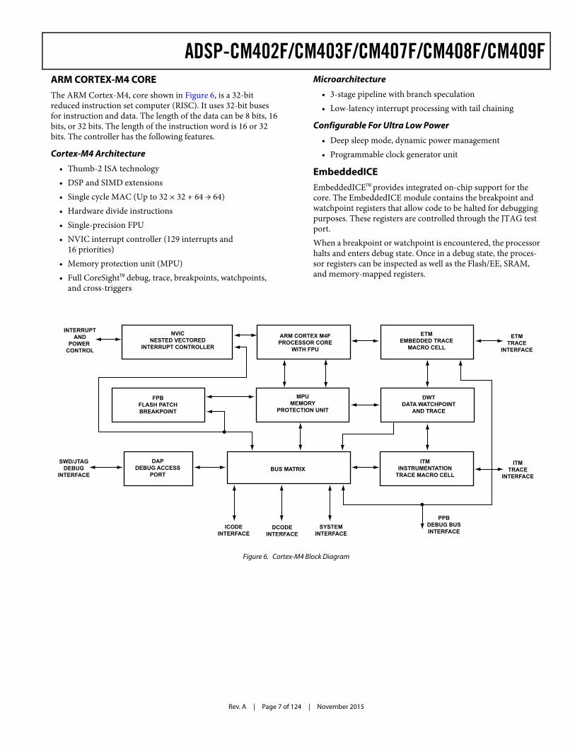
ADSP-CM402F/CM403F/CM407F/CM408F/CM409FARM CORTEX-M4 COREThe ARM Cortex-M4, core shown in Figure 6, is a 32-bit reduced instruction set computer (RISC). It uses 32-bit buses for instruction and data. The length of the data can be 8 bits, 16 bits, or 32 bits. The length of the instruction word is 16 or 32 bits. The controller has the following features.
Cortex-M4 Architecture
• Thumb-2 ISA technology• DSP and SIMD extensions• Single cycle MAC (Up to 32 × 32 + 64 → 64)• Hardware divide instructions• Single-precision FPU• NVIC interrupt controller (129 interrupts and
16 priorities)• Memory protection unit (MPU)• Full CoreSightTM debug, trace, breakpoints, watchpoints,
and cross-triggers
Microarchitecture
• 3-stage pipeline with branch speculation• Low-latency interrupt processing with tail chaining
Configurable For Ultra Low Power
• Deep sleep mode, dynamic power management• Programmable clock generator unit
EmbeddedICEEmbeddedICETM provides integrated on-chip support for the core. The EmbeddedICE module contains the breakpoint and watchpoint registers that allow code to be halted for debugging purposes. These registers are controlled through the JTAG test port.When a breakpoint or watchpoint is encountered, the processor halts and enters debug state. Once in a debug state, the proces-sor registers can be inspected as well as the Flash/EE, SRAM, and memory-mapped registers.
Figure 6. Cortex-M4 Block Diagram
NVICNESTED VECTORED
INTERRUPT CONTROLLER
MPUMEMORY
PROTECTION UNIT
BUS MATRIXDAP
DEBUG ACCESSPORT
ARM CORTEX M4FPROCESSOR CORE
WITH FPU
ETMEMBEDDED TRACE
MACRO CELL
ETMTRACE
INTERFACE
ITMTRACE
INTERFACE
INTERRUPTAND
POWER CONTROL
SWD/JTAGDEBUG
INTERFACE
FPBFLASH PATCHBREAKPOINT
DWTDATA WATCHPOINT
AND TRACE
ITMINSTRUMENTATION
TRACE MACRO CELL
PPBDEBUG BUSINTERFACE
ICODEINTERFACE
DCODEINTERFACE
SYSTEMINTERFACE

Rev. A | Page 8 of 124 | November 2015
ADSP-CM402F/CM403F/CM407F/CM408F/CM409FPROCESSOR INFRASTRUCTUREThe following sections provide information on the primary infrastructure components of the ADSP-CM40xF processors.
DMA Controllers (DDEs)
The processor contains 17 independent and concurrently oper-ating peripheral DMA channels plus two MDMA streams. DDE Channel 0 to Channel 16 are for peripherals and Channel 17 to Channel 20 are for MDMA.
System Event Controller (SEC)
The SEC manages the enabling and routing of system fault sources through its integrated fault management unit.
Trigger Routing Unit (TRU)
The TRU provides system-level sequence control without core intervention. The TRU maps trigger masters (generators of trig-gers) to trigger slaves (receivers of triggers). Slave endpoints can be configured to respond to triggers in various ways. Common applications enabled by the TRU include:
• Initiating the ADC sampling periodically in each PWM period or based on external events
• Automatically triggering the start of a DMA sequence after a sequence from another DMA channel completes
• Software triggering• Synchronization of concurrent activities
Pin Interrupts (PINT)
Every port pin on the processor can request interrupts in either an edge-sensitive or a level-sensitive manner with programma-ble polarity. Interrupt functionality is decoupled from GPIO operation. Six system-level interrupt channels (PINT0 to PINT5) are reserved for this purpose. Each of these interrupt channels can manage up to 32 interrupt pins. The assignment from pin to interrupt is not performed on a pin-by-pin basis. Rather, groups of eight pins (half ports) can be flexibly assigned to interrupt channels. Every pin interrupt channel features a special set of 32-bit mem-ory-mapped registers that enable half-port assignment and interrupt management. This includes masking, identification, and clearing of requests. These registers also enable access to the respective pin states and use of the interrupt latches, regardless of whether the interrupt is masked or not. Most control registers feature multiple MMR address entries to write-one-to-set or write-one-to-clear them individually.
General-Purpose I/O (GPIO)
Each general-purpose port pin can be individually controlled by manipulation of the port control, status, and interrupt registers:
• GPIO direction control register—Specifies the direction of each individual GPIO pin as input or output.
• GPIO control and status registers —A write one to modify mechanism allows any combination of individual GPIO pins to be modified in a single instruction, without affect-ing the level of any other GPIO pins.
• GPIO interrupt mask registers—Allow each individual GPIO pin to function as an interrupt to the processor. GPIO pins defined as inputs can be configured to generate hardware interrupts, while output pins can be triggered by software interrupts.
• GPIO interrupt sensitivity registers—Specify whether indi-vidual pins are level- or edge-sensitive and specify—if edge-sensitive—whether just the rising edge or both the ris-ing and falling edges of the signal are significant.
Pin Multiplexing
The processor supports a flexible multiplexing scheme that mul-tiplexes the GPIO pins with various peripherals. A maximum of five peripherals plus GPIO functionality is shared by each GPIO pin. All GPIO pins have a bypass path feature—that is, when the output enable and the input enable of a GPIO pin are both active, the data signal before the pad driver is looped back to the receive path for the same GPIO pin. For more information, see:
• ADSP-CM402F/ADSP-CM403F GPIO Multiplexing for 120-Lead LQFP on Page 27.
• ADSP-CM407F/ADSP-CM408F GPIO Multiplexing for 176-Lead LQFP on Page 37.
• ADSP-CM409F GPIO Multiplexing for 212-Ball BGA on Page 48.
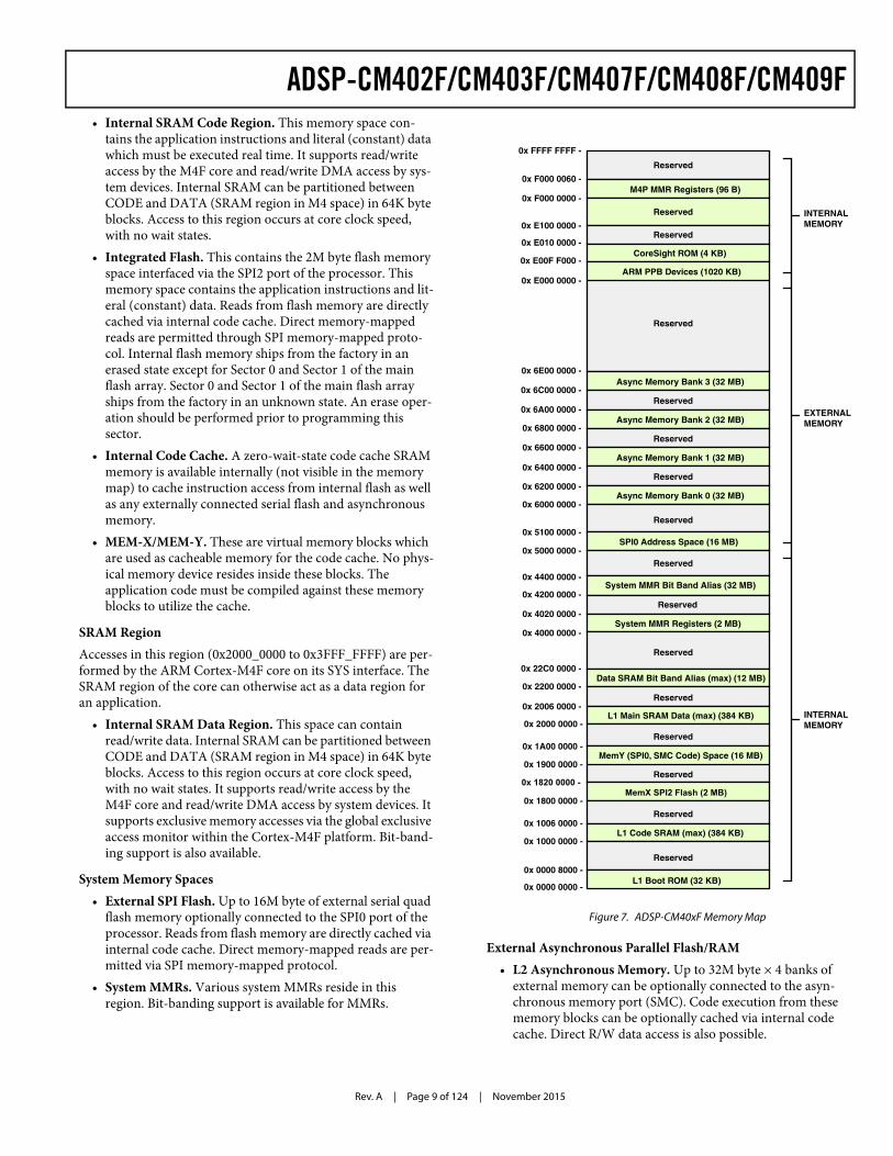
MEMORY ARCHITECTUREThe internal and external memory of the ADSP-CM40xF processor is shown in Figure 7 and described in the following sections.
ARM Cortex-M4 Memory Subsystem
The memory map of the ADSP-CM40xF family is based on the Cortex-M4 model from ARM. By retaining the standardized memory mapping, it becomes easier to port applications across M4 platforms. Only the physical implementation of memories inside the model differs from other vendors.ADSP-CM40xF application development is typically based on memory blocks across CODE/SRAM and external memory regions. Sufficient internal memory is available via internal SRAM and internal flash. Additional external memory devices may be interfaced via the SMC asynchronous memory port, as well as through the SPI0 serial memory interface.
Code RegionAccesses in this region (0x0000_0000 to 0x1FFF_FFFF) are per-formed by the core on its ICODE and DCODE interfaces, and they target the memory and cache resources within the Cortex-M4F platform integration component.
• Boot ROM. A 32K byte boot ROM executed at system reset. This space supports read-only access by the M4F core only. Note that ROM memory contents cannot be modified by the user.
Rev. A | Page 9 of 124 | November 2015
ADSP-CM402F/CM403F/CM407F/CM408F/CM409F• Internal SRAM Code Region. This memory space con-
tains the application instructions and literal (constant) data which must be executed real time. It supports read/write access by the M4F core and read/write DMA access by sys-tem devices. Internal SRAM can be partitioned between CODE and DATA (SRAM region in M4 space) in 64K byte blocks. Access to this region occurs at core clock speed, with no wait states.
• Integrated Flash. This contains the 2M byte flash memory space interfaced via the SPI2 port of the processor. This memory space contains the application instructions and lit-eral (constant) data. Reads from flash memory are directly cached via internal code cache. Direct memory-mapped reads are permitted through SPI memory-mapped proto-col. Internal flash memory ships from the factory in an erased state except for Sector 0 and Sector 1 of the main flash array. Sector 0 and Sector 1 of the main flash array ships from the factory in an unknown state. An erase oper-ation should be performed prior to programming this sector.
• Internal Code Cache. A zero-wait-state code cache SRAM memory is available internally (not visible in the memory map) to cache instruction access from internal flash as well as any externally connected serial flash and asynchronous memory.
• MEM-X/MEM-Y. These are virtual memory blocks which are used as cacheable memory for the code cache. No phys-ical memory device resides inside these blocks. The application code must be compiled against these memory blocks to utilize the cache.
SRAM RegionAccesses in this region (0x2000_0000 to 0x3FFF_FFFF) are per-formed by the ARM Cortex-M4F core on its SYS interface. The SRAM region of the core can otherwise act as a data region for an application.
• Internal SRAM Data Region. This space can contain read/write data. Internal SRAM can be partitioned between CODE and DATA (SRAM region in M4 space) in 64K byte blocks. Access to this region occurs at core clock speed, with no wait states. It supports read/write access by the M4F core and read/write DMA access by system devices. It supports exclusive memory accesses via the global exclusive access monitor within the Cortex-M4F platform. Bit-band-ing support is also available.
System Memory Spaces• External SPI Flash. Up to 16M byte of external serial quad
flash memory optionally connected to the SPI0 port of the processor. Reads from flash memory are directly cached via internal code cache. Direct memory-mapped reads are per-mitted via SPI memory-mapped protocol.
• System MMRs. Various system MMRs reside in this region. Bit-banding support is available for MMRs.
External Asynchronous Parallel Flash/RAM• L2 Asynchronous Memory. Up to 32M byte × 4 banks of
external memory can be optionally connected to the asyn-chronous memory port (SMC). Code execution from these memory blocks can be optionally cached via internal code cache. Direct R/W data access is also possible.
Figure 7. ADSP-CM40xF Memory Map
MemX SPI2 Flash (2 MB)0x 1820 0000 -
Rev. A | Page 10 of 124 | November 2015
ADSP-CM402F/CM403F/CM407F/CM408F/CM409FSystem RegionAccesses in this region (0xE000_0000 to 0xF7FF_FFFF) are per-formed by the ARM Cortex-M4F core on its SYS interface, and are handled within the Cortex-M4F platform. The MPU may be programmed to limit access to this space to privileged mode only.
• CoreSight ROM. The ROM table entries point to the debug components of the processor.
• ARM PPB Peripherals. This space is defined by ARM and occupies the bottom 256K byte of the SYS region (0xE000_0000 to 0xE004_0000). The space supports read/write access by the M4F core to the ARM core’s inter-nal peripherals (MPU, ITM, DWT, FPB, SCS, TPIU, ETM) and the CoreSight ROM. It is not accessible by system DMA.
• Platform Control Registers. This space has registers within the Cortex-M4F platform integration component that control the ARM core, its memory, and the code cache. It is accessible by the M4F core via its SYS port (but is not accessible by system DMA).
Static Memory Controller (SMC)
The SMC can be programmed to control up to four banks of external memories or memory-mapped devices, with very flexi-ble timing parameters. On ADSP-CM407F/CM408F/CM409F processors, each bank can occupy a 32M byte segment regard-less of the size of the device used.
Booting (BOOT)
The processor has several mechanisms for automatically loading internal and external memory after a reset. The boot mode is defined by the SYS_BMODE input pins dedicated for this pur-pose. There are two categories of boot modes. In master boot modes, the processor actively loads data from a serial memory. In slave boot modes, the processor receives data from external host devices. The boot modes are shown in Table 2. These modes are imple-mented by the SYS_BMODE bits of the RCU_CTL register and are sampled during power-on resets and software-initiated resets.
SYSTEM ACCELERATIONThe following sections describe the system acceleration blocks of the ADSP-CM40xF processors.
Harmonic Analysis Engine (HAE)
The harmonic analysis engine (HAE) block receives 8 kHz input samples from two source signals whose frequencies are between 45 Hz and 65 Hz. The HAE will then process the input samples and produce output results. The output results consist of power quality measurements of the fundamental and up to 12 select-able harmonics.
Sinus Cardinalis Filter (SINC)
The SINC module processes four bit streams using a pair of configurable SINC filters for each bitstream. The purpose of the primary SINC filter of each pair is to produce the filtered and decimated output for the pair. The output may be decimated to any integer rate between 8 and 256 times lower than the input rate. Greater decimation allows greater removal of noise and therefore greater ENOB.Optional additional filtering outside the SINC module may be used to further increase ENOB. The primary SINC filter output is accessible through transfer to processor memory, or to another peripheral, via DMA.Each of the four channels is also provided with a low-latency secondary filter with programmable positive and negative over-range detection comparators. These limit detection events can be used to interrupt the core, generate a trigger, or signal a sys-tem fault.
SECURITY FEATURESThe processor provides lightweight security functionality which protects sensitive data and IP located in the internal flash mem-ory. It includes password-protected slave boot modes (SPI and UART), as well as password-protected JTAG/SWD debug inter-faces. One of the safeguards of the security feature is the ability to perform bulk erase of the entire flash memory. Another secu-rity measure provides the ability to control which boot modes are allowed so as to protect the flash contents from untrusted or non-secure boot modes. Programs can enable or disable security features depending upon the secure header configured in inter-nal flash memory.Table 2. Boot Modes
SYS_BMODE[1:0] Setting Description00 No Boot/Idle. The processor does not boot.
Rather the boot kernel executes an IDLE instruction.
01 Flash Boot. Boot from integrated Flash memory through the SPI2.
10 SPI Slave Boot. Boot through the SPI0 peripheral configured as a slave.
11 UART Boot. Boot through the UART0 peripheral configured as a slave.
CAUTIONThis product includes security features that can be used to protect embedded nonvolatile memory contents and prevent execution of unauthorized code. When security is enabled on this device (either by the ordering party or the subsequent receiving parties), the ability of Analog Devices to conduct failure analysis on returned devices is limited. Contact Analog Devices for details on the failure analysis limitations for this device.
Rev. A | Page 11 of 124 | November 2015
ADSP-CM402F/CM403F/CM407F/CM408F/CM409FPROCESSOR RELIABILITY FEATURESThe processor provides the following features which can enhance or help achieve certain levels of system safety and reli-ability. While the level of safety is mainly dominated by system considerations, the following features are provided to enhance robustness.
Multi-Parity-Bit-Protected L1 Memories
In the processor’s SRAM and cache L1 memory space, each word is protected by multiple parity bits to detect the single event upsets that occur in all RAMs.
Cortex MPU
The MPU divides the memory map into a number of regions, and allows the system programmer to define the location, size, access permissions, and memory attributes of each region. It supports independent attribute settings for each region, over-lapping regions, and export of memory attributes to the system.For more information, refer to the ARM Infocenter web page.
System Protection Unit (SPU)
All system resources and L2 memory banks can be controlled by either the processor core, memory-to-memory DMA, or the debug unit. A system protection unit (SPU) enables write accesses to specific resources that are locked to a given master. System protection is enabled in greater granularity for some modules through a global lock concept.
Watchpoint Protection
The primary purpose of watchpoints and hardware breakpoints is to serve emulator needs. When enabled, they signal an emula-tor event whenever user-defined system resources are accessed or a core executes from user-defined addresses. Watchdog events can be configured such that they signal the events to the core or to the SEC.
Software Watchdog
The on-chip watchdog timer can provide software-based super-vision of the ADSP-CM40xF core.
Signal Watchdogs
The eight general-purpose timers feature two modes to monitor off-chip signals. The watchdog period mode monitors whether external signals toggle with a period within an expected range. The watchdog width mode monitors whether the pulse widths of external signals are in an expected range. Both modes help to detect incorrect undesired toggling (or lack thereof) of system-level signals.
Oscillator Watchdog
The oscillator watchdog monitors the external clock oscillator, and can detect the absence of clock as well as incorrect har-monic oscillation. The oscillator watchdog detection signal is routed to the fault management portion of the system event controller.
Low-Latency Sinc Filter Over-range Detection
The SINC filter units provide a low-latency secondary filter with programmable positive and negative limit detectors for each input channel. These may be used to monitor an isolation ADC bitstream for overrange or underrange conditions with a filter group delay as low as 0.7 μs on a 10 MHz bitstream. The sec-ondary SINC filter events can be used to interrupt the core, to trigger other events directly in hardware using the trigger rout-ing unit (TRU), or to signal the fault management unit of a system fault.
Up/Down Count Mismatch Detection
The GP counter can monitor external signal pairs, such as request/grant strobes. If the edge count mismatch exceeds the expected range, the up/down counter can flag this to the proces-sor or to the system event controller (SEC).
Fault Management
The fault management unit is part of the system event controller (SEC). Most system events can be defined as faults. If defined as such, the SEC forwards the event to its fault management unit which may automatically reset the entire device for reboot, or simply toggle the SYS_FAULT output pin to signal off-chip hardware. Optionally, the fault management unit can delay the action taken via a keyed sequence, to provide a final chance for the core to resolve the crisis and to prevent the fault action from being taken.
ADDITIONAL PROCESSOR PERIPHERALSThe processor contains a rich set of peripherals connected to the core via several concurrent high-bandwidth buses, providing flexibility in system configuration as well as excellent overall system performance (see Figure 1, Block Diagram). The processor contains high speed serial and parallel ports, an interrupt controller for flexible management of interrupts from the on-chip peripherals or external sources, and power manage-ment control functions to tailor the performance and power characteristics of the processor and system to many application scenarios.The following sections describe additional peripherals that were not described in the previous sections.
Timers
The processor includes several timers which are described in the following sections.
General-Purpose Timers (TIMER)The general-purpose (GP) timer unit provides eight general-purpose programmable timers. Each timer has an external pin that can be configured either as a pulse width modulator (PWM) or timer output, as an input to clock the timer, or as a mechanism for measuring pulse widths and periods of external events. These timers can be synchronized to an external clock input on the TM0_ACLKx pins, an external signal on the TM0_CLK input pin, or to the internal SCLK.
Rev. A | Page 12 of 124 | November 2015
ADSP-CM402F/CM403F/CM407F/CM408F/CM409FThe timer unit can be used in conjunction with the UARTs and the CAN controller to measure the width of the pulses in the data stream to provide a software auto-baud detect function for the respective serial channels. The timer can generate interrupts to the processor core, provid-ing periodic events for synchronization to either the system clock or to external signals. Timer events can also trigger other peripherals via the TRU (for instance, to signal a fault).
Watchdog Timer (WDT)The core includes a 32-bit timer, which may be used to imple-ment a software watchdog function. A software watchdog can improve system availability by forcing the processor to a known state, via generation of a general-purpose interrupt, if the timer expires before being reset by software. The programmer initial-izes the count value of the timer, enables the appropriate interrupt, then enables the timer. Thereafter, the software must reload the counter before it counts to zero from the pro-grammed value. This protects the system from remaining in an unknown state where software, which would normally reset the timer, has stopped running due to an external noise condition or software error. Optionally, the fault management unit (FMU) can directly initiate the processor reset upon the watchdog expiry event.
Capture Timer (CPTMR)The processor includes three instants of capture timers (CPTMR) to capture total on time. Each capture timer captures total on time of the input signal between two leading edges of the input trigger signal. Capture timer inputs to all the timers come from external pins and the input trigger signal comes from trigger routing unit (TRU).The core of the timer is a 32-bit counter which is reset at leading edge of the trigger and counts when the input signal level is active. The total on time of the input signal is captured from the counter at the leading edge of the trigger pulse. Capture timer can generate data interrupts to the processor core at leading edges of trigger pulses and status interrupts to indicate counter overflow condition.
3-Phase Pulse Width Modulator Unit (PWM)
The pulse width modulator (PWM) unit provides duty cycle and phase control capabilities to a resolution of one system clock cycle (SCLK). The heightened precision PWM (HPPWM) module provides increased performance to the PWM unit by increasing its resolution by several bits, resulting in enhanced precision levels. Additional features include:
• 16-bit center-based PWM generation unit• Programmable PWM pulse width• Single/double update modes• Programmable dead time and switching frequency• Twos-complement implementation which permits smooth
transition to full on and full off states• Dedicated asynchronous PWM trip signal
The eight PWM output signals (per PWM unit) consist of four high-side drive signals and four low-side drive signals. The polarity of a generated PWM signal can be set with software, so that either active high or active low PWM patterns can be produced.Each PWM block integrates a flexible and programmable 3-phase PWM waveform generator that can be programmed to generate the required switching patterns to drive a 3-phase voltage source inverter for ac induction motor (ACIM) or per-manent magnet synchronous motor (PMSM) control. In addition, the PWM block contains special functions that con-siderably simplify the generation of the required PWM switching patterns for control of the electronically commutated motor (ECM) or permanent magnet synchronous motor (PMSM) control. Software can enable a special mode for switched reluctance motors (SRM).Each PWM unit features a dedicated asynchronous trip pin which (when brought low) instantaneously places all PWM out-puts in the off state.
Serial Ports (SPORTs)
The synchronous serial ports provide an inexpensive interface to a wide variety of digital and mixed-signal peripheral devices such as Analog Devices, Inc., audio codecs, ADCs, and DACs. The serial ports are made up of two data lines per direction, a clock, and frame sync. The data lines can be programmed to either transmit or receive and each data line has a dedicated DMA channel.Serial port data can be automatically transferred to and from on-chip memory/external memory via dedicated DMA chan-nels.For full-duplex operation, two half SPORTs can work in conjunction with clock and frame sync signals shared internally through the SPMUX block. In some operation modes, SPORT supports gated clock. Serial ports operate in six modes:
• Standard DSP serial mode• Multichannel (TDM) mode• I2S mode• Packed I2S mode• Left-justified mode• Right-justified mode
General-Purpose Counters
The 32-bit counter can operate in general-purpose up/down count modes and can sense 2-bit quadrature or binary codes as typically emitted by industrial drives or manual thumbwheels. Count direction is either controlled by a level-sensitive input pin or by two edge detectors.A third counter input can provide flexible zero marker support and can alternatively be used to input the push-button signal of thumb wheels. All three pins have a programmable debouncing circuit.
Rev. A | Page 13 of 124 | November 2015
ADSP-CM402F/CM403F/CM407F/CM408F/CM409FThe GP counter can also support a programmable M/N fre-quency scaling of the CNT_CUD and CNT_CDG pins onto output pins in quadrature encoding mode.Internal signals forwarded to each general-purpose timer enable these timers to measure the intervals between count events. Boundary registers enable auto-zero operation or simple system warning by interrupts when programmable count values are exceeded.
Serial Peripheral Interface Ports (SPI)
The processor contains the SPI-compatible port that allows the processor to communicate with multiple SPI-compatible devices. In its simplest mode, the SPI interface uses three pins for trans-ferring data: two data pins master output-slave input and master input-slave output (SPI_MOSI and SPI_MISO) and a clock pin, SPI_CLK. A SPI chip select input pin (SPI_SS) lets other SPI devices select the processor, and three SPI chip select output pins (SPI_SELn) let the processor select other SPI devices. The SPI select pins are reconfigured general-purpose I/O pins. Using these pins, the SPI provides a full-duplex, synchronous serial interface, which supports both master and slave modes and multimaster environments. In a multimaster or multislave SPI system, the MOSI and MISO data output pins can be configured to behave as open drain out-puts (using the ODM bit) to prevent contention and possible damage to pin drivers. An external pull-up resistor is required on both the MOSI and MISO pins when this option is selected.When ODM is set and the SPI is configured as a master, the MOSI pin is three-stated when the data driven out on MOSI is a logic high. The MOSI pin is not three-stated when the driven data is a logic low. Similarly, when ODM is set and the SPI is configured as a slave, the MISO pin is three-stated if the data driven out on MISO is a logic high.The SPI port’s baud rate and clock phase/polarities are pro-grammable, and it has integrated DMA channels for both transmit and receive data streams.
Universal Asynchronous Receiver/Transmitter Ports (UART)
The processor provides full-duplex universal asynchronous receiver/transmitter (UART) ports, which are fully compatible with PC-standard UARTs. Each UART port provides a simpli-fied UART interface to other peripherals or hosts, supporting full-duplex, DMA-supported, asynchronous transfers of serial data. A UART port includes support for five to eight data bits, and none, even, or odd parity. Optionally, an additional address bit can be transferred to interrupt only addressed nodes in multi-drop bus (MDB) systems. A frame is terminated by one, one and a half, two or two and a half stop bits.The UART ports support automatic hardware flow control through the clear to send (CTS) input and request to send (RTS) output with programmable assertion FIFO levels.
To help support the local interconnect network (LIN) protocols, a special command causes the transmitter to queue a break command of programmable bit length into the transmit buffer. Similarly, the number of stop bits can be extended by a pro-grammable inter-frame space.The capabilities of the UARTs are further extended with sup-port for the infrared data association (IrDA®) serial infrared physical layer link specification (SIR) protocol.
2-Wire Controller Interface (TWI)
The processor includes a 2-wire interface (TWI) module for providing a simple exchange method of control data between multiple devices. The TWI module is compatible with the widely used I2C bus standard. The TWI module offers the capabilities of simultaneous master and slave operation and support for both 7-bit addressing and multimedia data arbitra-tion. The TWI interface utilizes two pins for transferring clock (TWI_SCL) and data (TWI_SDA) and supports the protocol at speeds up to 400k bits/sec. The TWI interface pins are compati-ble with 5 V logic levels.Additionally, the TWI module is fully compatible with serial camera control bus (SCCB) functionality for easier control of various CMOS camera sensor devices.
Controller Area Network (CAN)
The CAN controller implements the CAN 2.0B (active) proto-col. This protocol is an asynchronous communications protocol used in both industrial and automotive control systems. The CAN protocol is well suited for control applications due to its capability to communicate reliably over a network. This is because the protocol incorporates CRC checking, message error tracking, and fault node confinement. The CAN controller offers the following features:
• 32 mailboxes (8 receive only, 8 transmit only, 16 configu-rable for receive or transmit).
• Dedicated acceptance masks for each mailbox.• Additional data filtering on first two bytes.• Support for both the standard (11-bit) and extended
(29-bit) identifier (ID) message formats.• Support for remote frames.• Active or passive network support.• Interrupts, including: TX complete, RX complete, error
and global.An additional crystal is not required to supply the CAN clock, as the CAN clock is derived from a system clock through a pro-grammable divider.
10/100 Ethernet MAC (EMAC)
The processor can directly connect to a network by way of an embedded fast Ethernet media access controller (MAC) that supports both 10-BaseT (10M bits/sec) and 100-BaseT (100M bits/sec) operation. The 10/100 Ethernet MAC peripheral on the processor is fully compliant to the IEEE 802.3-2002 standard. It
Rev. A | Page 14 of 124 | November 2015
ADSP-CM402F/CM403F/CM407F/CM408F/CM409Fprovides programmable features designed to minimize supervi-sion, bus use, or message processing by the rest of the processor system. Some standard features are:
• Support for RMII protocols for external PHYs• Full-duplex and half-duplex modes• Media access management (in half-duplex operation)• Flow control • Station management: generation of MDC/MDIO frames
for read-write access to PHY registersSome advanced features are:
• Automatic checksum computation of IP header and IP payload fields of Rx frames
• Independent 32-bit descriptor-driven receive and transmit DMA channels
• Frame status delivery to memory through DMA, including frame completion semaphores for efficient buffer queue management in software
• Tx DMA support for separate descriptors for MAC header and payload to eliminate buffer copy operations
• Convenient frame alignment modes• 47 MAC management statistics counters with selectable
clear-on-read behavior and programmable interrupts on half maximum value
• Advanced power management• Magic packet detection and wakeup frame filtering• Support for 802.3Q tagged VLAN frames• Programmable MDC clock rate and preamble suppression
IEEE 1588 SupportThe IEEE 1588 standard is a precision clock synchronization protocol for networked measurement and control systems. The processor includes hardware support for IEEE 1588 with an integrated precision time protocol synchronization engine. This engine provides hardware assisted time stamping to improve the accuracy of clock synchronization between PTP nodes. The main features of the engine are:
• Support for both IEEE 1588-2002 and IEEE 1588-2008 pro-tocol standards
• 64-bit hardware assisted time stamping for transmit and receive frames capable of up to 10 ns resolution
• Identification of PTP message type, version, and PTP pay-load in frames sent directly over Ethernet and transmission of the status
• Coarse and fine correction methods for system time update• Alarm features: target time can be set to interrupt when
system time reaches target time
• Pulse-Per-Second (PPS) output for physical representation of the system time. Flexibility to control the pulse-per-sec-ond output signal including control of start time, stop time, PPS output width and interval
• Automatic detection and time stamping of PTP messages over IPv4, IPv6, and Ethernet packets
• Multiple input clock sources (SCLK, RMII clock, external clock)
• Auxiliary snapshot to time stamp external events
USB 2.0 On-the-Go (OTG) Dual-Role Device Controller
The USB 2.0 on-the go (OTG) dual-role device controller pro-vides a low-cost connectivity solution for the growing adoption of this bus standard in industrial applications, as well as con-sumer mobile devices such as cell phones, digital still cameras, and MP3 players. The USB 2.0 controller is a full-speed-only (FS) interface that allows these devices to transfer data using a point-to-point USB connection without the need for a PC host. The module can operate in a traditional USB peripheral-only mode as well as the host mode presented in the OTG supple-ment to the USB 2.0 specification.
CLOCK AND POWER MANAGEMENTThe processor provides three operating modes, each with a dif-ferent performance/power profile. Control of clocking to each of the processor peripherals also reduces power consumption. See Table 3 for a summary of the power settings for each mode.
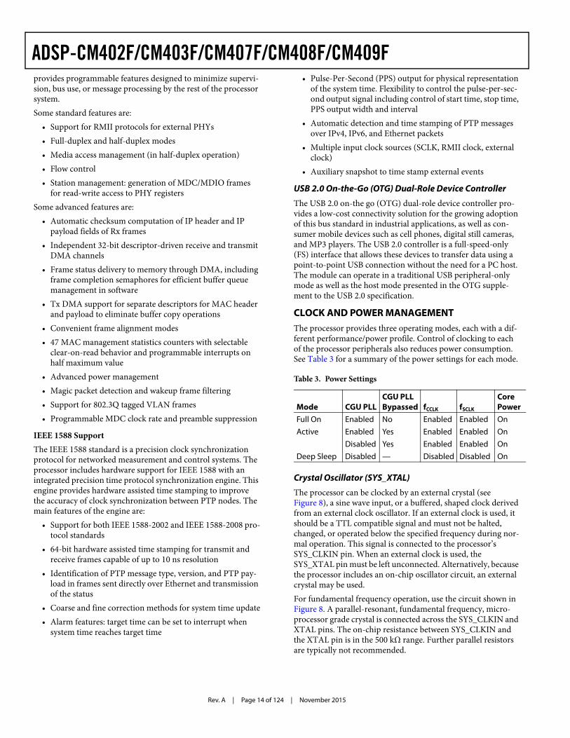
Crystal Oscillator (SYS_XTAL)
The processor can be clocked by an external crystal (see Figure 8), a sine wave input, or a buffered, shaped clock derived from an external clock oscillator. If an external clock is used, it should be a TTL compatible signal and must not be halted, changed, or operated below the specified frequency during nor-mal operation. This signal is connected to the processor’s SYS_CLKIN pin. When an external clock is used, the SYS_XTAL pin must be left unconnected. Alternatively, because the processor includes an on-chip oscillator circuit, an external crystal may be used.For fundamental frequency operation, use the circuit shown in Figure 8. A parallel-resonant, fundamental frequency, micro-processor grade crystal is connected across the SYS_CLKIN and XTAL pins. The on-chip resistance between SYS_CLKIN and the XTAL pin is in the 500 kΩ range. Further parallel resistors are typically not recommended.
Table 3. Power Settings
Mode CGU PLLCGU PLLBypassed fCCLK fSCLK
CorePower
Full On Enabled No Enabled Enabled OnActive Enabled Yes Enabled Enabled On
Disabled Yes Enabled Enabled OnDeep Sleep Disabled — Disabled Disabled On
Rev. A | Page 15 of 124 | November 2015
ADSP-CM402F/CM403F/CM407F/CM408F/CM409F
The two capacitors and the 330 Ω series resistor shown in Figure 8 fine tune phase and amplitude of the sine frequency. The capacitor and resistor values shown in Figure 8 are typical values only. The capacitor values are dependent upon the crystal manufacturers’ load capacitance recommendations and the PCB physical layout. The resistor value depends on the drive level specified by the crystal manufacturer. The user should verify the customized values based on careful investigations on multiple devices over temperature range.A third-overtone crystal can be used for frequencies above 25 MHz. The circuit is then modified to ensure crystal operation only at the third overtone by adding a tuned inductor circuit as shown in Figure 8. A design procedure for third-overtone operation is discussed in detail in application note (EE-168) “Using Third Overtone Crystals with the ADSP-218x DSP” (www.analog.com/ee-168).
Oscillator Watchdog
A programmable oscillator watchdog unit is provided to allow verification of proper startup and harmonic mode of the exter-nal crystal. This allows the user to specify the expected frequency of oscillation, and to enable detection of non-oscilla-tion and improper-oscillation faults. These events can be routed to the SYS_FAULT output pin and/or to cause a reset of the part.
Clock Generation Unit (CGU)
The clock generation unit (CGU) generates all on-chip clocks and synchronization signals. Multiplication factors are pro-grammed to the PLLs to define the PLLCLK frequency. Programmable values divide the PLLCLK frequency to generate the core clock (CCLK), the system clocks (SCLK), and the out-put clock (OCLK). This is illustrated in Figure 10 on Page 64.
Writing to the CGU control registers does not affect the behav-ior of the PLL immediately. Registers are first programmed with a new value, and the PLL logic executes the changes so that it transitions smoothly from the current conditions to the new ones. SYS_CLKIN oscillations start when power is applied to the VDD_EXT pins. The rising edge of SYS_HWRST can be applied as soon as all voltage supplies are within specifications (see Operating Conditions on Page 64), and SYS_CLKIN oscil-lations are stable.
Clock Out/External Clock
A SYS_CLKOUT output pin has programmable options to out-put divided-down versions of the on-chip clocks, including USB clocks. By default, the SYS_CLKOUT pin drives a buffered ver-sion of the SYS_CLKIN input. Clock generation faults (for example PLL unlock) may trigger a reset by hardware.SYS_CLKOUT can be used to output one of several different clocks used on the processor. The clocks shown in Table 4 can be outputs from SYS_CLKOUT.
Power Management
As shown in Table 5 and Figure 4 on Page 6, the processor requires three different power domains, VDD_INT, VDD_EXT, and VDD_ANA. By isolating the internal logic of the processor into its own power domain, separate from other I/O, the proces-sor can take advantage of dynamic power management without affecting the other I/O devices. There are no sequencing requirements for the various power domains, but all domains must be powered according to the appropriate Specifications table for processor operating conditions; even if the fea-ture/peripheral is not used.The dynamic power management feature of the processor allows the processor’s core clock frequency (fCCLK) to be dynam-ically controlled.
The power dissipated by a processor is largely a function of its clock frequency and the square of the operating voltage. For example, reducing the clock frequency by 25% results in a 25% reduction in dynamic power dissipation. For more information on power pins, see Operating Conditions on Page 64.
Figure 8. External Crystal Connection
SYS_CLKIN
TO PLL CIRCUITRY
FOR OVERTONEOPERATION ONLY:
NOTE: VALUES MARKED WITH * MUST BE CUSTOMIZED, DEPENDINGON THE CRYSTAL AND LAYOUT. ANALYZE CAREFULLY. FORFREQUENCIES ABOVE 33 MHz, THE SUGGESTED CAPACITOR VALUEOF 18pF SHOULD BE TREATED AS A MAXIMUM, AND THE SUGGESTED
18 pF* 18 pF *
*
ADSP-CM40xF
SYS_XTAL
Table 4. SYS_CLKOUT Source and Divider Options
Clock Source Divider CCLK (Core Clock) By 4OCLK (Output Clock) ProgrammableUSBCLK ProgrammableCLKBUF None, direct from SYS_CLKIN
Table 5. Power Domains
Power Domain VDD RangeAll Internal Logic VDD_INT
Digital I/O VDD_EXT
Analog VDD_ANA
Rev. A | Page 16 of 124 | November 2015
ADSP-CM402F/CM403F/CM407F/CM408F/CM409FFull-On Operating Mode—Maximum PerformanceIn the full-on mode, the PLL is enabled and is not bypassed, providing capability for maximum operational frequency. This is the execution state in which maximum performance can be achieved. The processor core and all enabled peripherals run at full speed.For more information about PLL controls, see the “Dynamic Power Management” chapter in the ADSP-CM40x Mixed-Signal Control Processor with ARM Cortex-M4 Hardware Reference.
Deep Sleep Operating Mode—Maximum Dynamic Power SavingsThe deep sleep mode maximizes dynamic power savings by dis-abling the clocks to the processor core and to all synchronous peripherals. Asynchronous peripherals may still be running but cannot access internal resources or external memory.
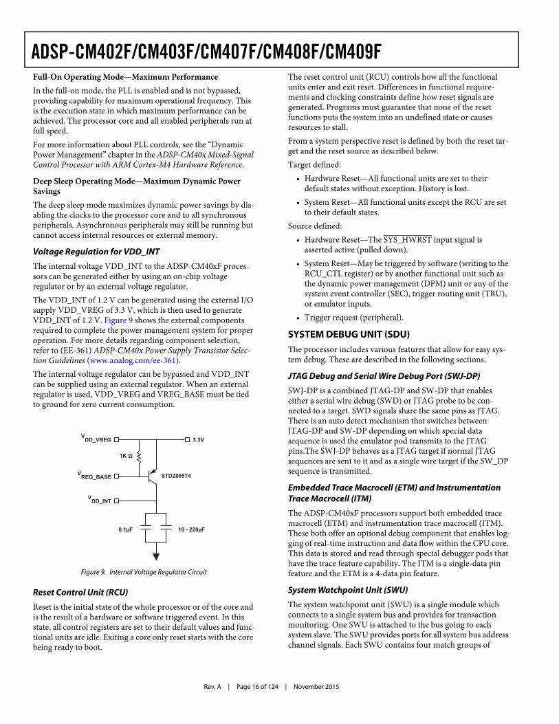
Voltage Regulation for VDD_INT
The internal voltage VDD_INT to the ADSP-CM40xF proces-sors can be generated either by using an on-chip voltage regulator or by an external voltage regulator.The VDD_INT of 1.2 V can be generated using the external I/O supply VDD_VREG of 3.3 V, which is then used to generate VDD_INT of 1.2 V. Figure 9 shows the external components required to complete the power management system for proper operation. For more details regarding component selection, refer to (EE-361) ADSP-CM40x Power Supply Transistor Selec-tion Guidelines (www.analog.com/ee-361).The internal voltage regulator can be bypassed and VDD_INT can be supplied using an external regulator. When an external regulator is used, VDD_VREG and VREG_BASE must be tied to ground for zero current consumption.
Reset Control Unit (RCU)
Reset is the initial state of the whole processor or of the core and is the result of a hardware or software triggered event. In this state, all control registers are set to their default values and func-tional units are idle. Exiting a core only reset starts with the core being ready to boot.
The reset control unit (RCU) controls how all the functional units enter and exit reset. Differences in functional require-ments and clocking constraints define how reset signals are generated. Programs must guarantee that none of the reset functions puts the system into an undefined state or causes resources to stall. From a system perspective reset is defined by both the reset tar-get and the reset source as described below.Target defined:
• Hardware Reset—All functional units are set to their default states without exception. History is lost.
• System Reset—All functional units except the RCU are set to their default states.
Source defined:• Hardware Reset—The SYS_HWRST input signal is
asserted active (pulled down).• System Reset—May be triggered by software (writing to the
RCU_CTL register) or by another functional unit such as the dynamic power management (DPM) unit or any of the system event controller (SEC), trigger routing unit (TRU), or emulator inputs.
• Trigger request (peripheral).
SYSTEM DEBUG UNIT (SDU)The processor includes various features that allow for easy sys-tem debug. These are described in the following sections.
JTAG Debug and Serial Wire Debug Port (SWJ-DP)
SWJ-DP is a combined JTAG-DP and SW-DP that enables either a serial wire debug (SWD) or JTAG probe to be con-nected to a target. SWD signals share the same pins as JTAG. There is an auto detect mechanism that switches between JTAG-DP and SW-DP depending on which special data sequence is used the emulator pod transmits to the JTAG pins.The SWJ-DP behaves as a JTAG target if normal JTAG sequences are sent to it and as a single wire target if the SW_DP sequence is transmitted.
Embedded Trace Macrocell (ETM) and Instrumentation Trace Macrocell (ITM)
The ADSP-CM40xF processors support both embedded trace macrocell (ETM) and instrumentation trace macrocell (ITM). These both offer an optional debug component that enables log-ging of real-time instruction and data flow within the CPU core. This data is stored and read through special debugger pods that have the trace feature capability. The ITM is a single-data pin feature and the ETM is a 4-data pin feature.
System Watchpoint Unit (SWU)
The system watchpoint unit (SWU) is a single module which connects to a single system bus and provides for transaction monitoring. One SWU is attached to the bus going to each system slave. The SWU provides ports for all system bus address channel signals. Each SWU contains four match groups of
Figure 9. Internal Voltage Regulator Circuit
VDD_VREG
STD2805T4
1K
VREG_BASE
VDD_INT
3.3V
10 - 220μF 0.1μF
VDD_VREG
STD2805T4
1K
VREG_BASE
VDD_INT
3.3V
10 - 220μF 0.1μF
VDD_VREG
STD2805T4
1K
VREG_BASE
VDD_INT
3.3V
10 - 220μF 0.1μF
Rev. A | Page 17 of 124 | November 2015
ADSP-CM402F/CM403F/CM407F/CM408F/CM409Fregisters with associated hardware. These four SWU match groups operate independently, but share common event (inter-rupt and trigger) outputs.
DEVELOPMENT TOOLSThe ADSP-CM40xF processor is supported with a set of highly sophisticated and easy-to-use development tools for embedded applications. For more information, see the Analog Devices website.
ADDITIONAL INFORMATIONThe following publications that describe the ADSP-CM40xF processors (and related processors) can be ordered from any Analog Devices sales office or accessed electronically on our website:
• ADSP-CM40x Mixed-Signal Control Processor with ARM Cortex-M4 Hardware Reference
• ADSP-CM402F/CM403F/CM407F/CM408F/CM409F Anomaly Sheet
This data sheet describes the ARM Cortex-M4 core and mem-ory architecture used on the ADSP-CM40xF processor, but does not provide detailed programming information for the ARM processor. For more information about programming the ARM processor, visit the ARM Infocenter web page.The applicable documentation for programming the ARM Cor-tex-M4 processor include:
• Cortex®-M4 Devices Generic User Guide• CoreSightTM ETMTM-M4 Technical Reference Manual• Cortex®-M4 Technical Reference Manual
RELATED SIGNAL CHAINSA signal chain is a series of signal-conditioning electronic com-ponents that receive input (data acquired from sampling either real-time phenomena or from stored data) in tandem, with the output of one portion of the chain supplying input to the next. Signal chains are often used in signal processing applications to gather and process data or to apply system controls based on analysis of real-time phenomena.Analog Devices eases signal processing system development by providing signal processing components that are designed to work together well. A tool for viewing relationships between specific applications and related components is available on the www.analog.com website.The application signal chains page in the Circuits from the Lab® site (http:\\www.analog.com\circuits) provides:
• Graphical circuit block diagram presentation of signal chains for a variety of circuit types and applications
• Drill down links for components in each chain to selection guides and application information
• Reference designs applying best practice design techniques
SECURITY FEATURES DISCLAIMERTo our knowledge, the Security Features, when used in accor-dance with the data sheet and hardware reference manual specifications, provide a secure method of implementing code and data safeguards. However, Analog Devices does not guaran-tee that this technology provides absolute security. ACCORDINGLY, ANALOG DEVICES HEREBY DISCLAIMS ANY AND ALL EXPRESS AND IMPLIED WARRANTIES THAT THE SECURITY FEATURES CANNOT BE BREACHED, COMPROMISED, OR OTHERWISE CIRCUM-VENTED AND IN NO EVENT SHALL ANALOG DEVICES BE LIABLE FOR ANY LOSS, DAMAGE, DESTRUCTION, OR RELEASE OF DATA, INFORMATION, PHYSICAL PROP-ERTY, OR INTELLECTUAL PROPERTY.
Rev. A | Page 18 of 124 | November 2015
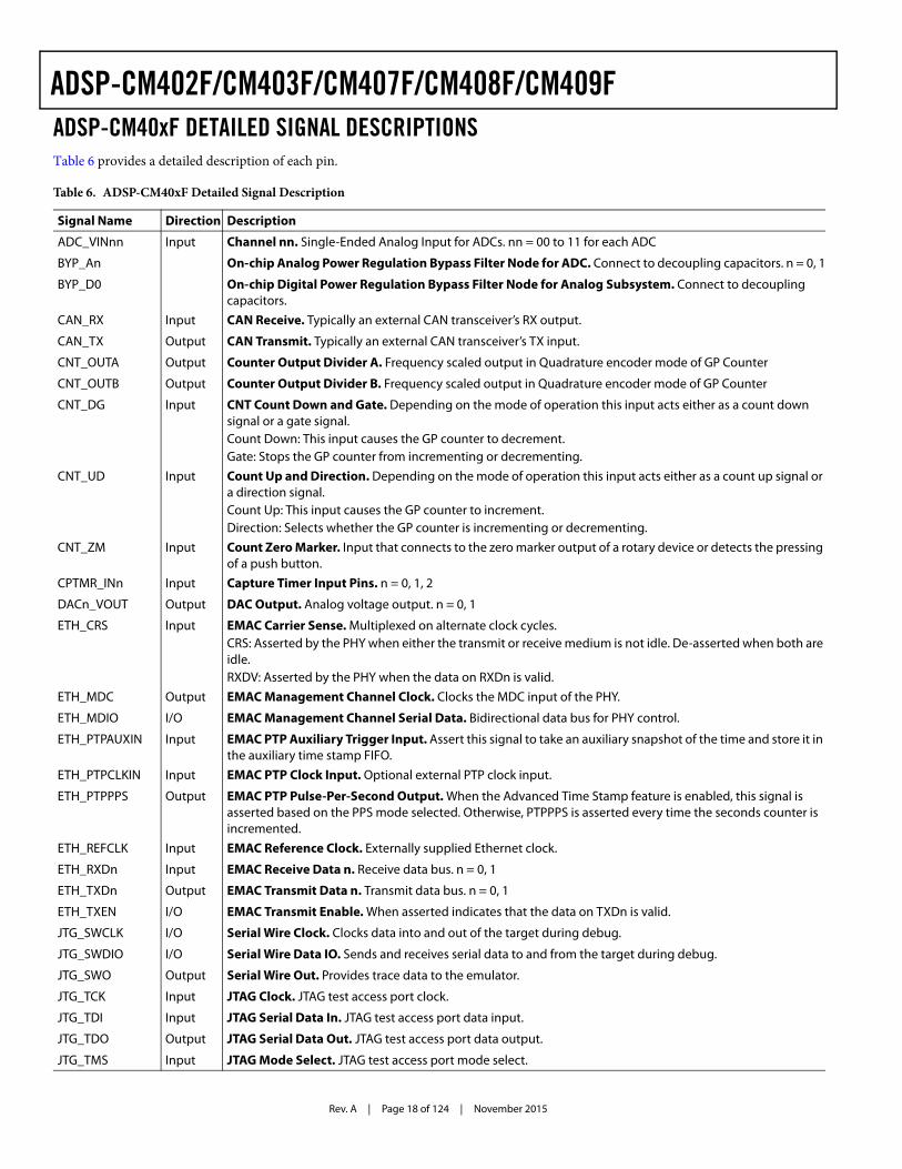
ADSP-CM402F/CM403F/CM407F/CM408F/CM409FADSP-CM40xF DETAILED SIGNAL DESCRIPTIONSTable 6 provides a detailed description of each pin.
Table 6. ADSP-CM40xF Detailed Signal Description
Signal Name Direction Description
ADC_VINnn Input Channel nn. Single-Ended Analog Input for ADCs. nn = 00 to 11 for each ADC
BYP_An On-chip Analog Power Regulation Bypass Filter Node for ADC. Connect to decoupling capacitors. n = 0, 1
BYP_D0 On-chip Digital Power Regulation Bypass Filter Node for Analog Subsystem. Connect to decoupling capacitors.
CAN_RX Input CAN Receive. Typically an external CAN transceiver’s RX output.
CAN_TX Output CAN Transmit. Typically an external CAN transceiver’s TX input.
CNT_OUTA Output Counter Output Divider A. Frequency scaled output in Quadrature encoder mode of GP Counter
CNT_OUTB Output Counter Output Divider B. Frequency scaled output in Quadrature encoder mode of GP Counter
CNT_DG Input CNT Count Down and Gate. Depending on the mode of operation this input acts either as a count down signal or a gate signal.Count Down: This input causes the GP counter to decrement.Gate: Stops the GP counter from incrementing or decrementing.
CNT_UD Input Count Up and Direction. Depending on the mode of operation this input acts either as a count up signal or a direction signal.Count Up: This input causes the GP counter to increment.Direction: Selects whether the GP counter is incrementing or decrementing.
CNT_ZM Input Count Zero Marker. Input that connects to the zero marker output of a rotary device or detects the pressing of a push button.
CPTMR_INn Input Capture Timer Input Pins. n = 0, 1, 2
DACn_VOUT Output DAC Output. Analog voltage output. n = 0, 1
ETH_CRS Input EMAC Carrier Sense. Multiplexed on alternate clock cycles.CRS: Asserted by the PHY when either the transmit or receive medium is not idle. De-asserted when both are idle.RXDV: Asserted by the PHY when the data on RXDn is valid.
ETH_MDC Output EMAC Management Channel Clock. Clocks the MDC input of the PHY.
ETH_MDIO I/O EMAC Management Channel Serial Data. Bidirectional data bus for PHY control.
ETH_PTPAUXIN Input EMAC PTP Auxiliary Trigger Input. Assert this signal to take an auxiliary snapshot of the time and store it in the auxiliary time stamp FIFO.
ETH_PTPCLKIN Input EMAC PTP Clock Input. Optional external PTP clock input.
ETH_PTPPPS Output EMAC PTP Pulse-Per-Second Output. When the Advanced Time Stamp feature is enabled, this signal is asserted based on the PPS mode selected. Otherwise, PTPPPS is asserted every time the seconds counter is incremented.
ETH_REFCLK Input EMAC Reference Clock. Externally supplied Ethernet clock.
ETH_RXDn Input EMAC Receive Data n. Receive data bus. n = 0, 1
ETH_TXDn Output EMAC Transmit Data n. Transmit data bus. n = 0, 1
ETH_TXEN I/O EMAC Transmit Enable. When asserted indicates that the data on TXDn is valid.
JTG_SWCLK I/O Serial Wire Clock. Clocks data into and out of the target during debug.
JTG_SWDIO I/O Serial Wire Data IO. Sends and receives serial data to and from the target during debug.
JTG_SWO Output Serial Wire Out. Provides trace data to the emulator.
JTG_TCK Input JTAG Clock. JTAG test access port clock.
JTG_TDI Input JTAG Serial Data In. JTAG test access port data input.
JTG_TDO Output JTAG Serial Data Out. JTAG test access port data output.
JTG_TMS Input JTAG Mode Select. JTAG test access port mode select.
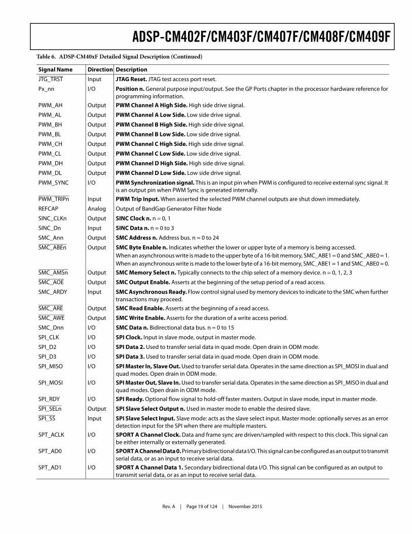
Rev. A | Page 19 of 124 | November 2015
ADSP-CM402F/CM403F/CM407F/CM408F/CM409F
JTG_TRST Input JTAG Reset. JTAG test access port reset.
Px_nn I/O Position n. General purpose input/output. See the GP Ports chapter in the processor hardware reference for programming information.
PWM_AH Output PWM Channel A High Side. High side drive signal.
PWM_AL Output PWM Channel A Low Side. Low side drive signal.
PWM_BH Output PWM Channel B High Side. High side drive signal.
PWM_BL Output PWM Channel B Low Side. Low side drive signal.
PWM_CH Output PWM Channel C High Side. High side drive signal.
PWM_CL Output PWM Channel C Low Side. Low side drive signal.
PWM_DH Output PWM Channel D High Side. High side drive signal.
PWM_DL Output PWM Channel D Low Side. Low side drive signal.
PWM_SYNC I/O PWM Synchronization signal. This is an input pin when PWM is configured to receive external sync signal. It is an output pin when PWM Sync is generated internally.
PWM_TRIPn Input PWM Trip Input. When asserted the selected PWM channel outputs are shut down immediately.
REFCAP Analog Output of BandGap Generator Filter Node
SINC_CLKn Output SINC Clock n. n = 0, 1
SINC_Dn Input SINC Data n. n = 0 to 3
SMC_Ann Output SMC Address n. Address bus. n = 0 to 24
SMC_ABEn Output SMC Byte Enable n. Indicates whether the lower or upper byte of a memory is being accessed. When an asynchronous write is made to the upper byte of a 16-bit memory, SMC_ABE1 = 0 and SMC_ABE0 = 1.When an asynchronous write is made to the lower byte of a 16-bit memory, SMC_ABE1 = 1 and SMC_ABE0 = 0.
SMC_AMSn Output SMC Memory Select n. Typically connects to the chip select of a memory device. n = 0, 1, 2, 3
SMC_AOE Output SMC Output Enable. Asserts at the beginning of the setup period of a read access.
SMC_ARDY Input SMC Asynchronous Ready. Flow control signal used by memory devices to indicate to the SMC when further transactions may proceed.
SMC_ARE Output SMC Read Enable. Asserts at the beginning of a read access.
SMC_AWE Output SMC Write Enable. Asserts for the duration of a write access period.
SMC_Dnn I/O SMC Data n. Bidirectional data bus. n = 0 to 15
SPI_CLK I/O SPI Clock. Input in slave mode, output in master mode.
SPI_D2 I/O SPI Data 2. Used to transfer serial data in quad mode. Open drain in ODM mode.
SPI_D3 I/O SPI Data 3. Used to transfer serial data in quad mode. Open drain in ODM mode.
SPI_MISO I/O SPI Master In, Slave Out. Used to transfer serial data. Operates in the same direction as SPI_MOSI in dual and quad modes. Open drain in ODM mode.
SPI_MOSI I/O SPI Master Out, Slave In. Used to transfer serial data. Operates in the same direction as SPI_MISO in dual and quad modes. Open drain in ODM mode.
SPI_RDY I/O SPI Ready. Optional flow signal to hold-off faster masters. Output in slave mode, input in master mode.
SPI_SELn Output SPI Slave Select Output n. Used in master mode to enable the desired slave.
SPI_SS Input SPI Slave Select Input. Slave mode: acts as the slave select input. Master mode: optionally serves as an error detection input for the SPI when there are multiple masters.
SPT_ACLK I/O SPORT A Channel Clock. Data and frame sync are driven/sampled with respect to this clock. This signal can be either internally or externally generated.
SPT_AD0 I/O SPORT A Channel Data 0. Primary bidirectional data I/O. This signal can be configured as an output to transmit serial data, or as an input to receive serial data.
SPT_AD1 I/O SPORT A Channel Data 1. Secondary bidirectional data I/O. This signal can be configured as an output to transmit serial data, or as an input to receive serial data.
Table 6. ADSP-CM40xF Detailed Signal Description (Continued)
Signal Name Direction Description
Rev. A | Page 20 of 124 | November 2015
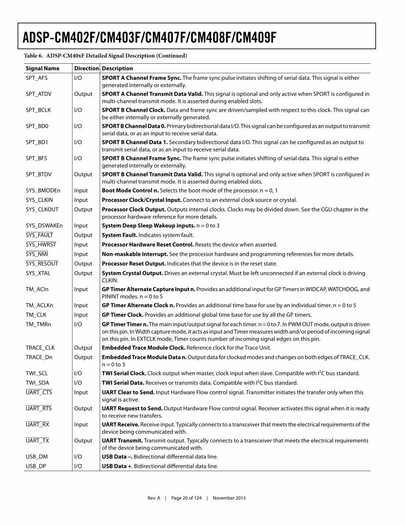
ADSP-CM402F/CM403F/CM407F/CM408F/CM409F
SPT_AFS I/O SPORT A Channel Frame Sync. The frame sync pulse initiates shifting of serial data. This signal is either generated internally or externally.
SPT_ATDV Output SPORT A Channel Transmit Data Valid. This signal is optional and only active when SPORT is configured in multi-channel transmit mode. It is asserted during enabled slots.
SPT_BCLK I/O SPORT B Channel Clock. Data and frame sync are driven/sampled with respect to this clock. This signal can be either internally or externally generated.
SPT_BD0 I/O SPORT B Channel Data 0. Primary bidirectional data I/O. This signal can be configured as an output to transmit serial data, or as an input to receive serial data.
SPT_BD1 I/O SPORT B Channel Data 1. Secondary bidirectional data I/O. This signal can be configured as an output to transmit serial data, or as an input to receive serial data.
SPT_BFS I/O SPORT B Channel Frame Sync. The frame sync pulse initiates shifting of serial data. This signal is either generated internally or externally.
SPT_BTDV Output SPORT B Channel Transmit Data Valid. This signal is optional and only active when SPORT is configured in multi-channel transmit mode. It is asserted during enabled slots.
SYS_BMODEn Input Boot Mode Control n. Selects the boot mode of the processor. n = 0, 1
SYS_CLKIN Input Processor Clock/Crystal Input. Connect to an external clock source or crystal.
SYS_CLKOUT Output Processor Clock Output. Outputs internal clocks. Clocks may be divided down. See the CGU chapter in the processor hardware reference for more details.
SYS_DSWAKEn Input System Deep Sleep Wakeup inputs. n = 0 to 3
SYS_FAULT Output System Fault. Indicates system fault.
SYS_HWRST Input Processor Hardware Reset Control. Resets the device when asserted.
SYS_NMI Input Non-maskable Interrupt. See the processor hardware and programming references for more details.
SYS_RESOUT Output Processor Reset Output. Indicates that the device is in the reset state.
SYS_XTAL Output System Crystal Output. Drives an external crystal. Must be left unconnected if an external clock is driving CLKIN.
TM_ACIn Input GP Timer Alternate Capture Input n. Provides an additional input for GP Timers in WIDCAP, WATCHDOG, and PININT modes. n = 0 to 5
TM_ACLKn Input GP Timer Alternate Clock n. Provides an additional time base for use by an individual timer. n = 0 to 5
TM_CLK Input GP Timer Clock. Provides an additional global time base for use by all the GP timers.
TM_TMRn I/O GP Timer Timer n. The main input/output signal for each timer. n = 0 to 7. In PWM OUT mode, output is driven on this pin. In Width capture mode, it acts as input and Timer measures width and/or period of incoming signal on this pin. In EXTCLK mode, Timer counts number of incoming signal edges on this pin.
TRACE_CLK Output Embedded Trace Module Clock. Reference clock for the Trace Unit.
TRACE_Dn Output Embedded Trace Module Data n. Output data for clocked modes and changes on both edges of TRACE_CLK. n = 0 to 3
TWI_SCL I/O TWI Serial Clock. Clock output when master, clock input when slave. Compatible with I2C bus standard.
TWI_SDA I/O TWI Serial Data. Receives or transmits data. Compatible with I2C bus standard.
UART_CTS Input UART Clear to Send. Input Hardware Flow control signal. Transmitter initiates the transfer only when this signal is active.
UART_RTS Output UART Request to Send. Output Hardware Flow control signal. Receiver activates this signal when it is ready to receive new transfers.
UART_RX Input UART Receive. Receive input. Typically connects to a transceiver that meets the electrical requirements of the device being communicated with.
UART_TX Output UART Transmit. Transmit output. Typically connects to a transceiver that meets the electrical requirements of the device being communicated with.
USB_DM I/O USB Data –. Bidirectional differential data line.
USB_DP I/O USB Data +. Bidirectional differential data line.
Table 6. ADSP-CM40xF Detailed Signal Description (Continued)
Signal Name Direction Description
Rev. A | Page 21 of 124 | November 2015
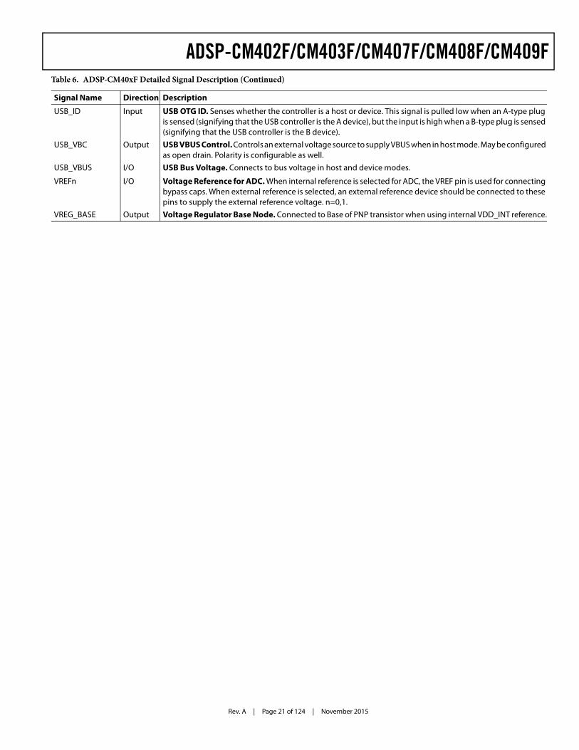
ADSP-CM402F/CM403F/CM407F/CM408F/CM409F
USB_ID Input USB OTG ID. Senses whether the controller is a host or device. This signal is pulled low when an A-type plug is sensed (signifying that the USB controller is the A device), but the input is high when a B-type plug is sensed (signifying that the USB controller is the B device).
USB_VBC Output USB VBUS Control. Controls an external voltage source to supply VBUS when in host mode. May be configured as open drain. Polarity is configurable as well.
USB_VBUS I/O USB Bus Voltage. Connects to bus voltage in host and device modes.
VREFn I/O Voltage Reference for ADC. When internal reference is selected for ADC, the VREF pin is used for connecting bypass caps. When external reference is selected, an external reference device should be connected to these pins to supply the external reference voltage. n=0,1.
VREG_BASE Output Voltage Regulator Base Node. Connected to Base of PNP transistor when using internal VDD_INT reference.
Table 6. ADSP-CM40xF Detailed Signal Description (Continued)
Signal Name Direction Description
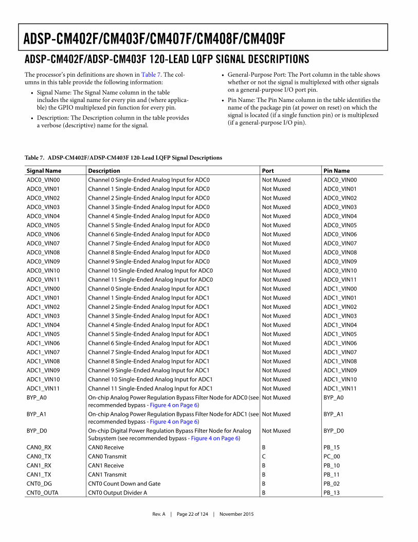
Rev. A | Page 22 of 124 | November 2015
ADSP-CM402F/CM403F/CM407F/CM408F/CM409FADSP-CM402F/ADSP-CM403F 120-LEAD LQFP SIGNAL DESCRIPTIONSThe processor’s pin definitions are shown in Table 7. The col-umns in this table provide the following information:
• Signal Name: The Signal Name column in the table includes the signal name for every pin and (where applica-ble) the GPIO multiplexed pin function for every pin.
• Description: The Description column in the table provides a verbose (descriptive) name for the signal.
• General-Purpose Port: The Port column in the table shows whether or not the signal is multiplexed with other signals on a general-purpose I/O port pin.
• Pin Name: The Pin Name column in the table identifies the name of the package pin (at power on reset) on which the signal is located (if a single function pin) or is multiplexed (if a general-purpose I/O pin).
Table 7. ADSP-CM402F/ADSP-CM403F 120-Lead LQFP Signal Descriptions
Signal Name Description Port Pin NameADC0_VIN00 Channel 0 Single-Ended Analog Input for ADC0 Not Muxed ADC0_VIN00ADC0_VIN01 Channel 1 Single-Ended Analog Input for ADC0 Not Muxed ADC0_VIN01ADC0_VIN02 Channel 2 Single-Ended Analog Input for ADC0 Not Muxed ADC0_VIN02ADC0_VIN03 Channel 3 Single-Ended Analog Input for ADC0 Not Muxed ADC0_VIN03ADC0_VIN04 Channel 4 Single-Ended Analog Input for ADC0 Not Muxed ADC0_VIN04ADC0_VIN05 Channel 5 Single-Ended Analog Input for ADC0 Not Muxed ADC0_VIN05ADC0_VIN06 Channel 6 Single-Ended Analog Input for ADC0 Not Muxed ADC0_VIN06ADC0_VIN07 Channel 7 Single-Ended Analog Input for ADC0 Not Muxed ADC0_VIN07ADC0_VIN08 Channel 8 Single-Ended Analog Input for ADC0 Not Muxed ADC0_VIN08ADC0_VIN09 Channel 9 Single-Ended Analog Input for ADC0 Not Muxed ADC0_VIN09ADC0_VIN10 Channel 10 Single-Ended Analog Input for ADC0 Not Muxed ADC0_VIN10ADC0_VIN11 Channel 11 Single-Ended Analog Input for ADC0 Not Muxed ADC0_VIN11ADC1_VIN00 Channel 0 Single-Ended Analog Input for ADC1 Not Muxed ADC1_VIN00ADC1_VIN01 Channel 1 Single-Ended Analog Input for ADC1 Not Muxed ADC1_VIN01ADC1_VIN02 Channel 2 Single-Ended Analog Input for ADC1 Not Muxed ADC1_VIN02ADC1_VIN03 Channel 3 Single-Ended Analog Input for ADC1 Not Muxed ADC1_VIN03ADC1_VIN04 Channel 4 Single-Ended Analog Input for ADC1 Not Muxed ADC1_VIN04ADC1_VIN05 Channel 5 Single-Ended Analog Input for ADC1 Not Muxed ADC1_VIN05ADC1_VIN06 Channel 6 Single-Ended Analog Input for ADC1 Not Muxed ADC1_VIN06ADC1_VIN07 Channel 7 Single-Ended Analog Input for ADC1 Not Muxed ADC1_VIN07ADC1_VIN08 Channel 8 Single-Ended Analog Input for ADC1 Not Muxed ADC1_VIN08ADC1_VIN09 Channel 9 Single-Ended Analog Input for ADC1 Not Muxed ADC1_VIN09ADC1_VIN10 Channel 10 Single-Ended Analog Input for ADC1 Not Muxed ADC1_VIN10ADC1_VIN11 Channel 11 Single-Ended Analog Input for ADC1 Not Muxed ADC1_VIN11BYP_A0 On-chip Analog Power Regulation Bypass Filter Node for ADC0 (see
recommended bypass - Figure 4 on Page 6)Not Muxed BYP_A0
BYP_A1 On-chip Analog Power Regulation Bypass Filter Node for ADC1 (see recommended bypass - Figure 4 on Page 6)
Not Muxed BYP_A1
BYP_D0 On-chip Digital Power Regulation Bypass Filter Node for Analog Subsystem (see recommended bypass - Figure 4 on Page 6)
Not Muxed BYP_D0
CAN0_RX CAN0 Receive B PB_15CAN0_TX CAN0 Transmit C PC_00CAN1_RX CAN1 Receive B PB_10CAN1_TX CAN1 Transmit B PB_11CNT0_DG CNT0 Count Down and Gate B PB_02CNT0_OUTA CNT0 Output Divider A B PB_13
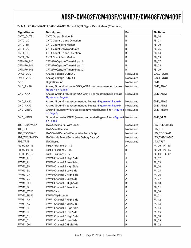
Rev. A | Page 23 of 124 | November 2015
ADSP-CM402F/CM403F/CM407F/CM408F/CM409F
CNT0_OUTB CNT0 Output Divider B B PB_14CNT0_UD CNT0 Count Up and Direction B PB_01CNT0_ZM CNT0 Count Zero Marker B PB_00CNT1_DG CNT1 Count Down and Gate B PB_05CNT1_UD CNT1 Count Up and Direction B PB_04CNT1_ZM CNT1 Count Zero Marker B PB_03CPTMR0_IN0 CPTMR0 Capture Timer0 Input 0 B PB_07CPTMR0_IN1 CPTMR0 Capture Timer0 Input 1 B PB_08CPTMR0_IN2 CPTMR0 Capture Timer0 Input 2 B PB_09DAC0_VOUT Analog Voltage Output 0 Not Muxed DAC0_VOUTDAC1_VOUT Analog Voltage Output 1 Not Muxed DAC1_VOUTGND Digital Ground Not Muxed GNDGND_ANA0 Analog Ground return for VDD_ANA0 (see recommended bypass -
Figure 4 on Page 6)Not Muxed GND_ANA0
GND_ANA1 Analog Ground return for VDD_ANA1 (see recommended bypass - Figure 4 on Page 6)
Not Muxed GND_ANA1
GND_ANA2 Analog Ground (see recommended bypass - Figure 4 on Page 6) Not Muxed GND_ANA2GND_ANA3 Analog Ground (see recommended bypass - Figure 4 on Page 6) Not Muxed GND_ANA3GND_VREF0 Ground return for VREF0 (see recommended bypass filter - Figure 4
on Page 6)Not Muxed GND_VREF0
GND_VREF1 Ground return for VREF1 (see recommended bypass filter - Figure 4 on Page 6)
Not Muxed GND_VREF1
JTG_TCK/SWCLK JTAG Clock/Serial Wire Clock Not Muxed JTG_TCK/SWCLKJTG_TDI JTAG Serial Data In Not Muxed JTG_TDIJTG_TDO/SWO JTAG Serial Data Out/Serial Wire Trace Output Not Muxed JTG_TDO/SWOJTG_TMS/SWDIO JTAG Mode Select/Serial Wire Debug Data I/O Not Muxed JTG_TMS/SWDIOJTG_TRST JTAG Reset Not Muxed JTG_TRSTPA_00-PA_15 Port A Positions 0 – 15 A PA_00 – PA_15PB_00-PB_15 Port B Positions 0 – 15 B PB_00 – PB_15PC_00-PC_07 Port C Positions 0 – 7 C PC_00 – PC_07PWM0_AH PWM0 Channel A High Side A PA_02PWM0_AL PWM0 Channel A Low Side A PA_03PWM0_BH PWM0 Channel B High Side A PA_04PWM0_BL PWM0 Channel B Low Side A PA_05PWM0_CH PWM0 Channel C High Side A PA_06PWM0_CL PWM0 Channel C Low Side A PA_07PWM0_DH PWM0 Channel D High Side B PB_00PWM0_DL PWM0 Channel D Low Side B PB_01PWM0_SYNC PWM0 Sync A PA_00PWM0_TRIP0 PWM0 Trip Input 0 A PA_01PWM1_AH PWM1 Channel A High Side A PA_12PWM1_AL PWM1 Channel A Low Side A PA_13PWM1_BH PWM1 Channel B High Side A PA_14PWM1_BL PWM1 Channel B Low Side A PA_15PWM1_CH PWM1 Channel C High Side A PA_08PWM1_CL PWM1 Channel C Low Side A PA_09PWM1_DH PWM1 Channel D High Side B PB_02
Table 7. ADSP-CM402F/ADSP-CM403F 120-Lead LQFP Signal Descriptions (Continued)
Signal Name Description Port Pin Name
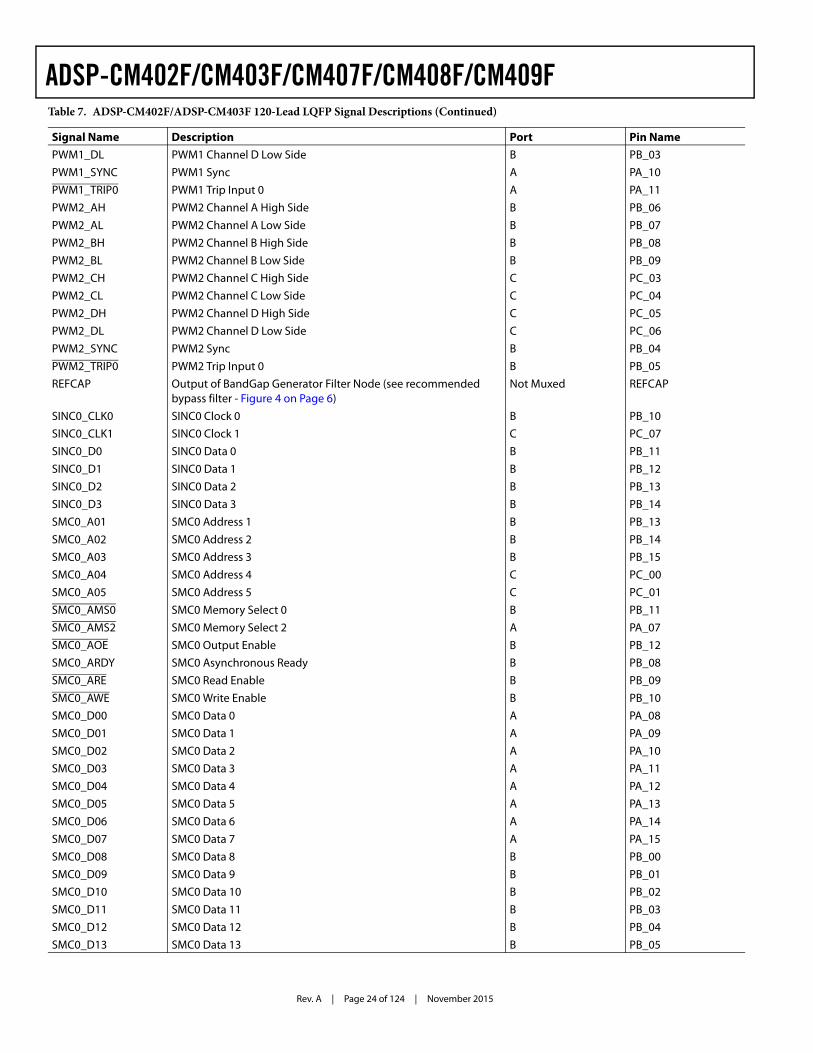
Rev. A | Page 24 of 124 | November 2015
ADSP-CM402F/CM403F/CM407F/CM408F/CM409F
PWM1_DL PWM1 Channel D Low Side B PB_03PWM1_SYNC PWM1 Sync A PA_10PWM1_TRIP0 PWM1 Trip Input 0 A PA_11PWM2_AH PWM2 Channel A High Side B PB_06PWM2_AL PWM2 Channel A Low Side B PB_07PWM2_BH PWM2 Channel B High Side B PB_08PWM2_BL PWM2 Channel B Low Side B PB_09PWM2_CH PWM2 Channel C High Side C PC_03PWM2_CL PWM2 Channel C Low Side C PC_04PWM2_DH PWM2 Channel D High Side C PC_05PWM2_DL PWM2 Channel D Low Side C PC_06PWM2_SYNC PWM2 Sync B PB_04PWM2_TRIP0 PWM2 Trip Input 0 B PB_05REFCAP Output of BandGap Generator Filter Node (see recommended
bypass filter - Figure 4 on Page 6)Not Muxed REFCAP
SINC0_CLK0 SINC0 Clock 0 B PB_10SINC0_CLK1 SINC0 Clock 1 C PC_07SINC0_D0 SINC0 Data 0 B PB_11SINC0_D1 SINC0 Data 1 B PB_12SINC0_D2 SINC0 Data 2 B PB_13SINC0_D3 SINC0 Data 3 B PB_14SMC0_A01 SMC0 Address 1 B PB_13SMC0_A02 SMC0 Address 2 B PB_14SMC0_A03 SMC0 Address 3 B PB_15SMC0_A04 SMC0 Address 4 C PC_00SMC0_A05 SMC0 Address 5 C PC_01SMC0_AMS0 SMC0 Memory Select 0 B PB_11SMC0_AMS2 SMC0 Memory Select 2 A PA_07SMC0_AOE SMC0 Output Enable B PB_12SMC0_ARDY SMC0 Asynchronous Ready B PB_08SMC0_ARE SMC0 Read Enable B PB_09SMC0_AWE SMC0 Write Enable B PB_10SMC0_D00 SMC0 Data 0 A PA_08SMC0_D01 SMC0 Data 1 A PA_09SMC0_D02 SMC0 Data 2 A PA_10SMC0_D03 SMC0 Data 3 A PA_11SMC0_D04 SMC0 Data 4 A PA_12SMC0_D05 SMC0 Data 5 A PA_13SMC0_D06 SMC0 Data 6 A PA_14SMC0_D07 SMC0 Data 7 A PA_15SMC0_D08 SMC0 Data 8 B PB_00SMC0_D09 SMC0 Data 9 B PB_01SMC0_D10 SMC0 Data 10 B PB_02SMC0_D11 SMC0 Data 11 B PB_03SMC0_D12 SMC0 Data 12 B PB_04SMC0_D13 SMC0 Data 13 B PB_05
Table 7. ADSP-CM402F/ADSP-CM403F 120-Lead LQFP Signal Descriptions (Continued)
Signal Name Description Port Pin Name
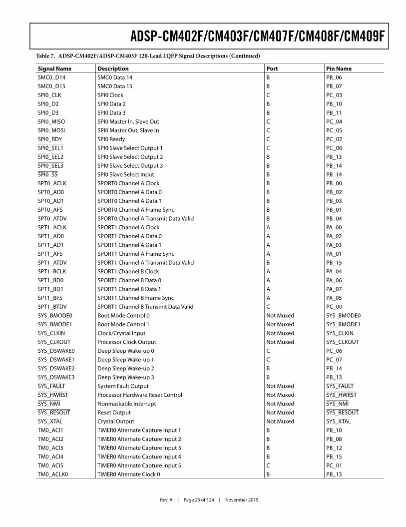
Rev. A | Page 25 of 124 | November 2015
ADSP-CM402F/CM403F/CM407F/CM408F/CM409F
SMC0_D14 SMC0 Data 14 B PB_06SMC0_D15 SMC0 Data 15 B PB_07SPI0_CLK SPI0 Clock C PC_03SPI0_D2 SPI0 Data 2 B PB_10SPI0_D3 SPI0 Data 3 B PB_11SPI0_MISO SPI0 Master In, Slave Out C PC_04SPI0_MOSI SPI0 Master Out, Slave In C PC_05SPI0_RDY SPI0 Ready C PC_02SPI0_SEL1 SPI0 Slave Select Output 1 C PC_06SPI0_SEL2 SPI0 Slave Select Output 2 B PB_13SPI0_SEL3 SPI0 Slave Select Output 3 B PB_14SPI0_SS SPI0 Slave Select Input B PB_14SPT0_ACLK SPORT0 Channel A Clock B PB_00SPT0_AD0 SPORT0 Channel A Data 0 B PB_02SPT0_AD1 SPORT0 Channel A Data 1 B PB_03SPT0_AFS SPORT0 Channel A Frame Sync B PB_01SPT0_ATDV SPORT0 Channel A Transmit Data Valid B PB_04SPT1_ACLK SPORT1 Channel A Clock A PA_00SPT1_AD0 SPORT1 Channel A Data 0 A PA_02SPT1_AD1 SPORT1 Channel A Data 1 A PA_03SPT1_AFS SPORT1 Channel A Frame Sync A PA_01SPT1_ATDV SPORT1 Channel A Transmit Data Valid B PB_15SPT1_BCLK SPORT1 Channel B Clock A PA_04SPT1_BD0 SPORT1 Channel B Data 0 A PA_06SPT1_BD1 SPORT1 Channel B Data 1 A PA_07SPT1_BFS SPORT1 Channel B Frame Sync A PA_05SPT1_BTDV SPORT1 Channel B Transmit Data Valid C PC_00SYS_BMODE0 Boot Mode Control 0 Not Muxed SYS_BMODE0SYS_BMODE1 Boot Mode Control 1 Not Muxed SYS_BMODE1SYS_CLKIN Clock/Crystal Input Not Muxed SYS_CLKINSYS_CLKOUT Processor Clock Output Not Muxed SYS_CLKOUTSYS_DSWAKE0 Deep Sleep Wake-up 0 C PC_06SYS_DSWAKE1 Deep Sleep Wake-up 1 C PC_07SYS_DSWAKE2 Deep Sleep Wake-up 2 B PB_14SYS_DSWAKE3 Deep Sleep Wake-up 3 B PB_13SYS_FAULT System Fault Output Not Muxed SYS_FAULTSYS_HWRST Processor Hardware Reset Control Not Muxed SYS_HWRSTSYS_NMI Nonmaskable Interrupt Not Muxed SYS_NMISYS_RESOUT Reset Output Not Muxed SYS_RESOUTSYS_XTAL Crystal Output Not Muxed SYS_XTALTM0_ACI1 TIMER0 Alternate Capture Input 1 B PB_10TM0_ACI2 TIMER0 Alternate Capture Input 2 B PB_08TM0_ACI3 TIMER0 Alternate Capture Input 3 B PB_12TM0_ACI4 TIMER0 Alternate Capture Input 4 B PB_15TM0_ACI5 TIMER0 Alternate Capture Input 5 C PC_01TM0_ACLK0 TIMER0 Alternate Clock 0 B PB_13
Table 7. ADSP-CM402F/ADSP-CM403F 120-Lead LQFP Signal Descriptions (Continued)
Signal Name Description Port Pin Name
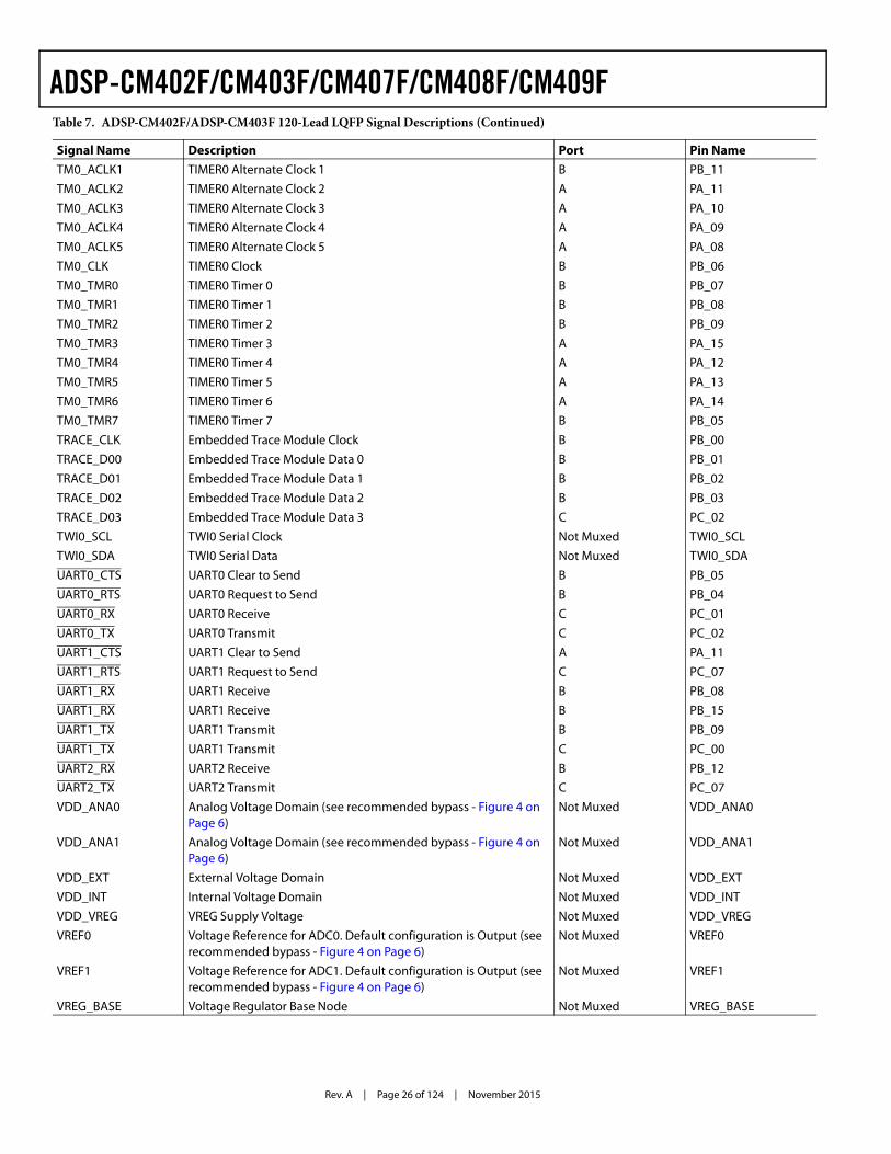
Rev. A | Page 26 of 124 | November 2015
ADSP-CM402F/CM403F/CM407F/CM408F/CM409F
TM0_ACLK1 TIMER0 Alternate Clock 1 B PB_11TM0_ACLK2 TIMER0 Alternate Clock 2 A PA_11TM0_ACLK3 TIMER0 Alternate Clock 3 A PA_10TM0_ACLK4 TIMER0 Alternate Clock 4 A PA_09TM0_ACLK5 TIMER0 Alternate Clock 5 A PA_08TM0_CLK TIMER0 Clock B PB_06TM0_TMR0 TIMER0 Timer 0 B PB_07TM0_TMR1 TIMER0 Timer 1 B PB_08TM0_TMR2 TIMER0 Timer 2 B PB_09TM0_TMR3 TIMER0 Timer 3 A PA_15TM0_TMR4 TIMER0 Timer 4 A PA_12TM0_TMR5 TIMER0 Timer 5 A PA_13TM0_TMR6 TIMER0 Timer 6 A PA_14TM0_TMR7 TIMER0 Timer 7 B PB_05TRACE_CLK Embedded Trace Module Clock B PB_00TRACE_D00 Embedded Trace Module Data 0 B PB_01TRACE_D01 Embedded Trace Module Data 1 B PB_02TRACE_D02 Embedded Trace Module Data 2 B PB_03TRACE_D03 Embedded Trace Module Data 3 C PC_02TWI0_SCL TWI0 Serial Clock Not Muxed TWI0_SCLTWI0_SDA TWI0 Serial Data Not Muxed TWI0_SDAUART0_CTS UART0 Clear to Send B PB_05UART0_RTS UART0 Request to Send B PB_04UART0_RX UART0 Receive C PC_01UART0_TX UART0 Transmit C PC_02UART1_CTS UART1 Clear to Send A PA_11UART1_RTS UART1 Request to Send C PC_07UART1_RX UART1 Receive B PB_08UART1_RX UART1 Receive B PB_15UART1_TX UART1 Transmit B PB_09UART1_TX UART1 Transmit C PC_00UART2_RX UART2 Receive B PB_12UART2_TX UART2 Transmit C PC_07VDD_ANA0 Analog Voltage Domain (see recommended bypass - Figure 4 on
Page 6)Not Muxed VDD_ANA0
VDD_ANA1 Analog Voltage Domain (see recommended bypass - Figure 4 on Page 6)
Not Muxed VDD_ANA1
VDD_EXT External Voltage Domain Not Muxed VDD_EXTVDD_INT Internal Voltage Domain Not Muxed VDD_INTVDD_VREG VREG Supply Voltage Not Muxed VDD_VREGVREF0 Voltage Reference for ADC0. Default configuration is Output (see
recommended bypass - Figure 4 on Page 6)Not Muxed VREF0
VREF1 Voltage Reference for ADC1. Default configuration is Output (see recommended bypass - Figure 4 on Page 6)
Not Muxed VREF1
VREG_BASE Voltage Regulator Base Node Not Muxed VREG_BASE
Table 7. ADSP-CM402F/ADSP-CM403F 120-Lead LQFP Signal Descriptions (Continued)
Signal Name Description Port Pin Name
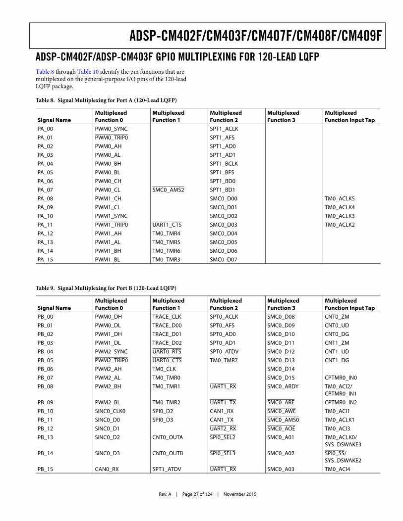
Rev. A | Page 27 of 124 | November 2015
ADSP-CM402F/CM403F/CM407F/CM408F/CM409FADSP-CM402F/ADSP-CM403F GPIO MULTIPLEXING FOR 120-LEAD LQFPTable 8 through Table 10 identify the pin functions that are multiplexed on the general-purpose I/O pins of the 120-lead LQFP package.
Table 8. Signal Multiplexing for Port A (120-Lead LQFP)
Signal NameMultiplexed Function 0
Multiplexed Function 1
Multiplexed Function 2
Multiplexed Function 3
Multiplexed Function Input Tap
PA_00 PWM0_SYNC SPT1_ACLKPA_01 PWM0_TRIP0 SPT1_AFSPA_02 PWM0_AH SPT1_AD0PA_03 PWM0_AL SPT1_AD1PA_04 PWM0_BH SPT1_BCLKPA_05 PWM0_BL SPT1_BFSPA_06 PWM0_CH SPT1_BD0PA_07 PWM0_CL SMC0_AMS2 SPT1_BD1PA_08 PWM1_CH SMC0_D00 TM0_ACLK5PA_09 PWM1_CL SMC0_D01 TM0_ACLK4PA_10 PWM1_SYNC SMC0_D02 TM0_ACLK3PA_11 PWM1_TRIP0 UART1_CTS SMC0_D03 TM0_ACLK2PA_12 PWM1_AH TM0_TMR4 SMC0_D04PA_13 PWM1_AL TM0_TMR5 SMC0_D05PA_14 PWM1_BH TM0_TMR6 SMC0_D06PA_15 PWM1_BL TM0_TMR3 SMC0_D07
Table 9. Signal Multiplexing for Port B (120-Lead LQFP)
Signal NameMultiplexed Function 0
Multiplexed Function 1
Multiplexed Function 2
Multiplexed Function 3
Multiplexed Function Input Tap
PB_00 PWM0_DH TRACE_CLK SPT0_ACLK SMC0_D08 CNT0_ZMPB_01 PWM0_DL TRACE_D00 SPT0_AFS SMC0_D09 CNT0_UDPB_02 PWM1_DH TRACE_D01 SPT0_AD0 SMC0_D10 CNT0_DGPB_03 PWM1_DL TRACE_D02 SPT0_AD1 SMC0_D11 CNT1_ZMPB_04 PWM2_SYNC UART0_RTS SPT0_ATDV SMC0_D12 CNT1_UDPB_05 PWM2_TRIP0 UART0_CTS TM0_TMR7 SMC0_D13 CNT1_DGPB_06 PWM2_AH TM0_CLK SMC0_D14PB_07 PWM2_AL TM0_TMR0 SMC0_D15 CPTMR0_IN0PB_08 PWM2_BH TM0_TMR1 UART1_RX SMC0_ARDY TM0_ACI2/
CPTMR0_IN1PB_09 PWM2_BL TM0_TMR2 UART1_TX SMC0_ARE CPTMR0_IN2PB_10 SINC0_CLK0 SPI0_D2 CAN1_RX SMC0_AWE TM0_ACI1PB_11 SINC0_D0 SPI0_D3 CAN1_TX SMC0_AMS0 TM0_ACLK1PB_12 SINC0_D1 UART2_RX SMC0_AOE TM0_ACI3PB_13 SINC0_D2 CNT0_OUTA SPI0_SEL2 SMC0_A01 TM0_ACLK0/
SYS_DSWAKE3PB_14 SINC0_D3 CNT0_OUTB SPI0_SEL3 SMC0_A02 SPI0_SS/
SYS_DSWAKE2PB_15 CAN0_RX SPT1_ATDV UART1_RX SMC0_A03 TM0_ACI4
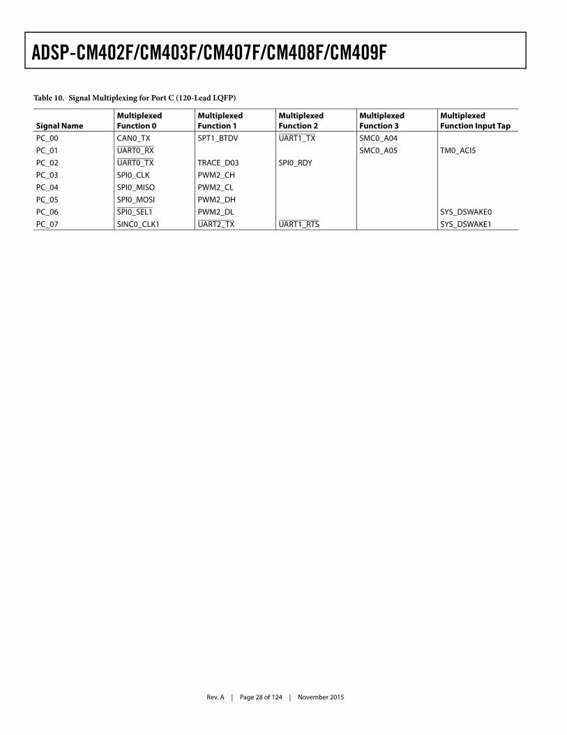
Rev. A | Page 28 of 124 | November 2015
ADSP-CM402F/CM403F/CM407F/CM408F/CM409F
Table 10. Signal Multiplexing for Port C (120-Lead LQFP)
Signal NameMultiplexed Function 0
Multiplexed Function 1
Multiplexed Function 2
Multiplexed Function 3
Multiplexed Function Input Tap
PC_00 CAN0_TX SPT1_BTDV UART1_TX SMC0_A04PC_01 UART0_RX SMC0_A05 TM0_ACI5PC_02 UART0_TX TRACE_D03 SPI0_RDYPC_03 SPI0_CLK PWM2_CHPC_04 SPI0_MISO PWM2_CLPC_05 SPI0_MOSI PWM2_DHPC_06 SPI0_SEL1 PWM2_DL SYS_DSWAKE0PC_07 SINC0_CLK1 UART2_TX UART1_RTS SYS_DSWAKE1
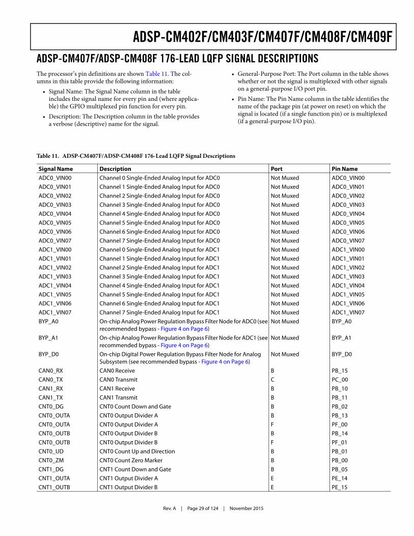
Rev. A | Page 29 of 124 | November 2015
ADSP-CM402F/CM403F/CM407F/CM408F/CM409FADSP-CM407F/ADSP-CM408F 176-LEAD LQFP SIGNAL DESCRIPTIONSThe processor’s pin definitions are shown Table 11. The col-umns in this table provide the following information:
• Signal Name: The Signal Name column in the table includes the signal name for every pin and (where applica-ble) the GPIO multiplexed pin function for every pin.
• Description: The Description column in the table provides a verbose (descriptive) name for the signal.
• General-Purpose Port: The Port column in the table shows whether or not the signal is multiplexed with other signals on a general-purpose I/O port pin.
• Pin Name: The Pin Name column in the table identifies the name of the package pin (at power on reset) on which the signal is located (if a single function pin) or is multiplexed (if a general-purpose I/O pin).
Table 11. ADSP-CM407F/ADSP-CM408F 176-Lead LQFP Signal Descriptions
Signal Name Description Port Pin NameADC0_VIN00 Channel 0 Single-Ended Analog Input for ADC0 Not Muxed ADC0_VIN00ADC0_VIN01 Channel 1 Single-Ended Analog Input for ADC0 Not Muxed ADC0_VIN01ADC0_VIN02 Channel 2 Single-Ended Analog Input for ADC0 Not Muxed ADC0_VIN02ADC0_VIN03 Channel 3 Single-Ended Analog Input for ADC0 Not Muxed ADC0_VIN03ADC0_VIN04 Channel 4 Single-Ended Analog Input for ADC0 Not Muxed ADC0_VIN04ADC0_VIN05 Channel 5 Single-Ended Analog Input for ADC0 Not Muxed ADC0_VIN05ADC0_VIN06 Channel 6 Single-Ended Analog Input for ADC0 Not Muxed ADC0_VIN06ADC0_VIN07 Channel 7 Single-Ended Analog Input for ADC0 Not Muxed ADC0_VIN07ADC1_VIN00 Channel 0 Single-Ended Analog Input for ADC1 Not Muxed ADC1_VIN00ADC1_VIN01 Channel 1 Single-Ended Analog Input for ADC1 Not Muxed ADC1_VIN01ADC1_VIN02 Channel 2 Single-Ended Analog Input for ADC1 Not Muxed ADC1_VIN02ADC1_VIN03 Channel 3 Single-Ended Analog Input for ADC1 Not Muxed ADC1_VIN03ADC1_VIN04 Channel 4 Single-Ended Analog Input for ADC1 Not Muxed ADC1_VIN04ADC1_VIN05 Channel 5 Single-Ended Analog Input for ADC1 Not Muxed ADC1_VIN05ADC1_VIN06 Channel 6 Single-Ended Analog Input for ADC1 Not Muxed ADC1_VIN06ADC1_VIN07 Channel 7 Single-Ended Analog Input for ADC1 Not Muxed ADC1_VIN07BYP_A0 On-chip Analog Power Regulation Bypass Filter Node for ADC0 (see
recommended bypass - Figure 4 on Page 6)Not Muxed BYP_A0
BYP_A1 On-chip Analog Power Regulation Bypass Filter Node for ADC1 (see recommended bypass - Figure 4 on Page 6)
Not Muxed BYP_A1
BYP_D0 On-chip Digital Power Regulation Bypass Filter Node for Analog Subsystem (see recommended bypass - Figure 4 on Page 6)
Not Muxed BYP_D0
CAN0_RX CAN0 Receive B PB_15CAN0_TX CAN0 Transmit C PC_00CAN1_RX CAN1 Receive B PB_10CAN1_TX CAN1 Transmit B PB_11CNT0_DG CNT0 Count Down and Gate B PB_02CNT0_OUTA CNT0 Output Divider A B PB_13CNT0_OUTA CNT0 Output Divider A F PF_00CNT0_OUTB CNT0 Output Divider B B PB_14CNT0_OUTB CNT0 Output Divider B F PF_01CNT0_UD CNT0 Count Up and Direction B PB_01CNT0_ZM CNT0 Count Zero Marker B PB_00CNT1_DG CNT1 Count Down and Gate B PB_05CNT1_OUTA CNT1 Output Divider A E PE_14CNT1_OUTB CNT1 Output Divider B E PE_15
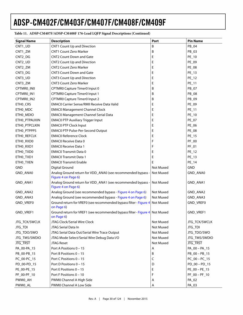
Rev. A | Page 30 of 124 | November 2015
ADSP-CM402F/CM403F/CM407F/CM408F/CM409F
CNT1_UD CNT1 Count Up and Direction B PB_04CNT1_ZM CNT1 Count Zero Marker B PB_03CNT2_DG CNT2 Count Down and Gate E PE_10CNT2_UD CNT2 Count Up and Direction E PE_09CNT2_ZM CNT2 Count Zero Marker E PE_08CNT3_DG CNT3 Count Down and Gate E PE_13CNT3_UD CNT3 Count Up and Direction E PE_12CNT3_ZM CNT3 Count Zero Marker E PE_11CPTMR0_IN0 CPTMR0 Capture Timer0 Input 0 B PB_07CPTMR0_IN1 CPTMR0 Capture Timer0 Input 1 B PB_08CPTMR0_IN2 CPTMR0 Capture Timer0 Input 2 B PB_09ETH0_CRS EMAC0 Carrier Sense/RMII Receive Data Valid E PE_09ETH0_MDC EMAC0 Management Channel Clock E PE_11ETH0_MDIO EMAC0 Management Channel Serial Data E PE_10ETH0_PTPAUXIN EMAC0 PTP Auxiliary Trigger Input E PE_07ETH0_PTPCLKIN EMAC0 PTP Clock Input E PE_06ETH0_PTPPPS EMAC0 PTP Pulse-Per-Second Output E PE_08ETH0_REFCLK EMAC0 Reference Clock E PE_15ETH0_RXD0 EMAC0 Receive Data 0 F PF_00ETH0_RXD1 EMAC0 Receive Data 1 F PF_01ETH0_TXD0 EMAC0 Transmit Data 0 E PE_12ETH0_TXD1 EMAC0 Transmit Data 1 E PE_13ETH0_TXEN EMAC0 Transmit Enable E PE_14GND Digital Ground Not Muxed GNDGND_ANA0 Analog Ground return for VDD_ANA0 (see recommended bypass -
Figure 4 on Page 6)Not Muxed GND_ANA0
GND_ANA1 Analog Ground return for VDD_ANA1 (see recommended bypass - Figure 4 on Page 6)
Not Muxed GND_ANA1
GND_ANA2 Analog Ground (see recommended bypass - Figure 4 on Page 6) Not Muxed GND_ANA2GND_ANA3 Analog Ground (see recommended bypass - Figure 4 on Page 6) Not Muxed GND_ANA3GND_VREF0 Ground return for VREF0 (see recommended bypass filter - Figure 4
on Page 6)Not Muxed GND_VREF0
GND_VREF1 Ground return for VREF1 (see recommended bypass filter - Figure 4 on Page 6)
Not Muxed GND_VREF1
JTG_TCK/SWCLK JTAG Clock/Serial Wire Clock Not Muxed JTG_TCK/SWCLKJTG_TDI JTAG Serial Data In Not Muxed JTG_TDIJTG_TDO/SWO JTAG Serial Data Out/Serial Wire Trace Output Not Muxed JTG_TDO/SWOJTG_TMS/SWDIO JTAG Mode Select/Serial Wire Debug Data I/O Not Muxed JTG_TMS/SWDIOJTG_TRST JTAG Reset Not Muxed JTG_TRSTPA_00-PA_15 Port A Positions 0 – 15 A PA_00 – PA_15PB_00-PB_15 Port B Positions 0 – 15 B PB_00 – PB_15PC_00-PC_15 Port C Positions 0 – 15 C PC_00 – PC_15PD_00-PD_15 Port D Positions 0 – 15 D PD_00 – PD_15PE_00-PE_15 Port E Positions 0 – 15 E PE_00 – PE_15PF_00-PF_10 Port F Positions 0 – 10 F PF_00 – PF_10PWM0_AH PWM0 Channel A High Side A PA_02PWM0_AL PWM0 Channel A Low Side A PA_03
Table 11. ADSP-CM407F/ADSP-CM408F 176-Lead LQFP Signal Descriptions (Continued)
Signal Name Description Port Pin Name
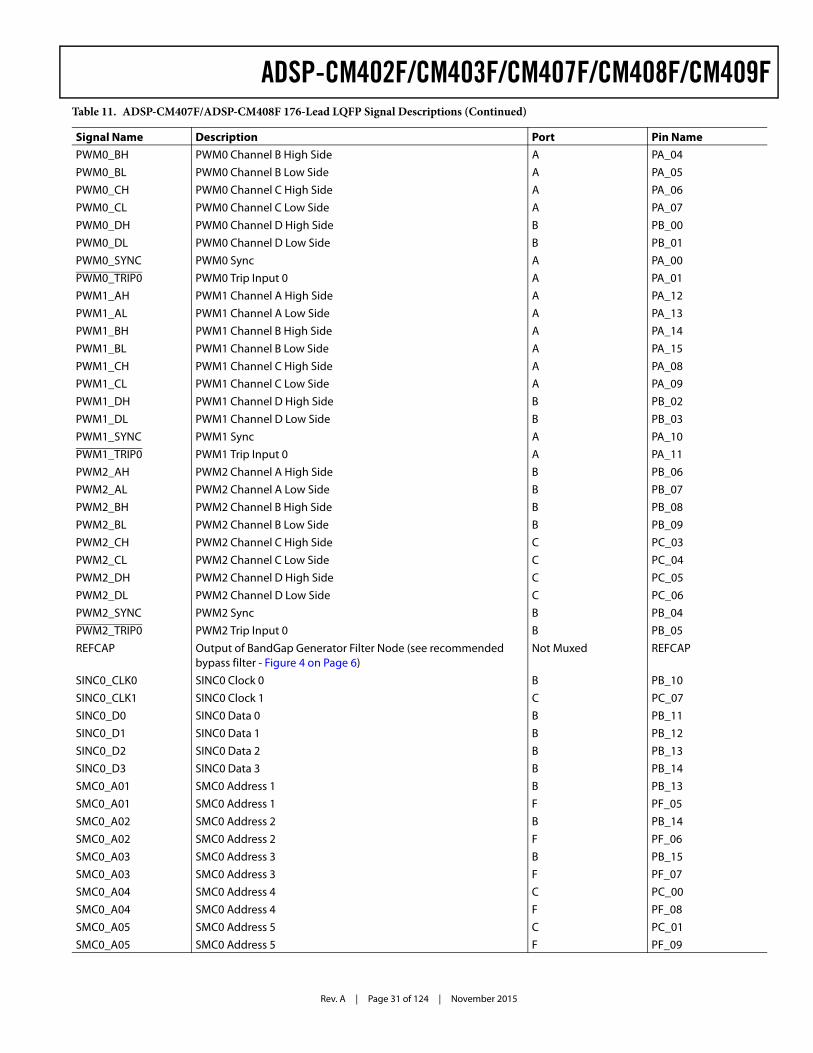
Rev. A | Page 31 of 124 | November 2015
ADSP-CM402F/CM403F/CM407F/CM408F/CM409F
PWM0_BH PWM0 Channel B High Side A PA_04PWM0_BL PWM0 Channel B Low Side A PA_05PWM0_CH PWM0 Channel C High Side A PA_06PWM0_CL PWM0 Channel C Low Side A PA_07PWM0_DH PWM0 Channel D High Side B PB_00PWM0_DL PWM0 Channel D Low Side B PB_01PWM0_SYNC PWM0 Sync A PA_00PWM0_TRIP0 PWM0 Trip Input 0 A PA_01PWM1_AH PWM1 Channel A High Side A PA_12PWM1_AL PWM1 Channel A Low Side A PA_13PWM1_BH PWM1 Channel B High Side A PA_14PWM1_BL PWM1 Channel B Low Side A PA_15PWM1_CH PWM1 Channel C High Side A PA_08PWM1_CL PWM1 Channel C Low Side A PA_09PWM1_DH PWM1 Channel D High Side B PB_02PWM1_DL PWM1 Channel D Low Side B PB_03PWM1_SYNC PWM1 Sync A PA_10PWM1_TRIP0 PWM1 Trip Input 0 A PA_11PWM2_AH PWM2 Channel A High Side B PB_06PWM2_AL PWM2 Channel A Low Side B PB_07PWM2_BH PWM2 Channel B High Side B PB_08PWM2_BL PWM2 Channel B Low Side B PB_09PWM2_CH PWM2 Channel C High Side C PC_03PWM2_CL PWM2 Channel C Low Side C PC_04PWM2_DH PWM2 Channel D High Side C PC_05PWM2_DL PWM2 Channel D Low Side C PC_06PWM2_SYNC PWM2 Sync B PB_04PWM2_TRIP0 PWM2 Trip Input 0 B PB_05REFCAP Output of BandGap Generator Filter Node (see recommended
bypass filter - Figure 4 on Page 6)Not Muxed REFCAP
SINC0_CLK0 SINC0 Clock 0 B PB_10SINC0_CLK1 SINC0 Clock 1 C PC_07SINC0_D0 SINC0 Data 0 B PB_11SINC0_D1 SINC0 Data 1 B PB_12SINC0_D2 SINC0 Data 2 B PB_13SINC0_D3 SINC0 Data 3 B PB_14SMC0_A01 SMC0 Address 1 B PB_13SMC0_A01 SMC0 Address 1 F PF_05SMC0_A02 SMC0 Address 2 B PB_14SMC0_A02 SMC0 Address 2 F PF_06SMC0_A03 SMC0 Address 3 B PB_15SMC0_A03 SMC0 Address 3 F PF_07SMC0_A04 SMC0 Address 4 C PC_00SMC0_A04 SMC0 Address 4 F PF_08SMC0_A05 SMC0 Address 5 C PC_01SMC0_A05 SMC0 Address 5 F PF_09
Table 11. ADSP-CM407F/ADSP-CM408F 176-Lead LQFP Signal Descriptions (Continued)
Signal Name Description Port Pin Name
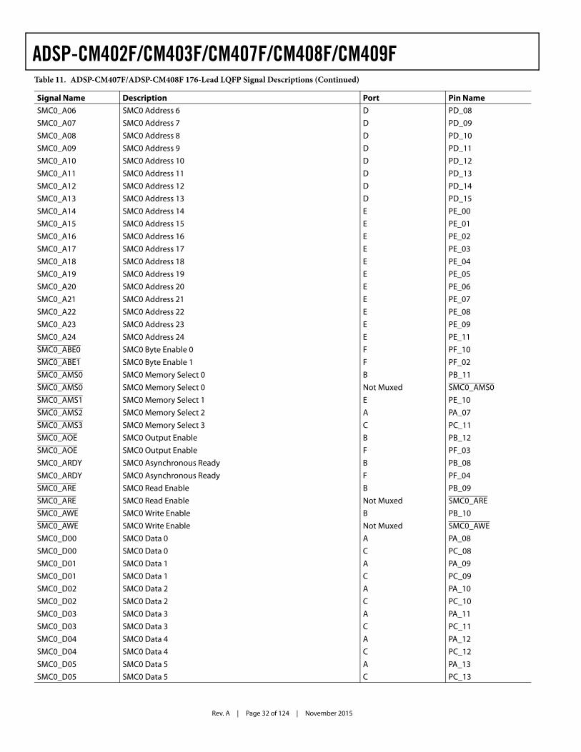
Rev. A | Page 32 of 124 | November 2015
ADSP-CM402F/CM403F/CM407F/CM408F/CM409F
SMC0_A06 SMC0 Address 6 D PD_08SMC0_A07 SMC0 Address 7 D PD_09SMC0_A08 SMC0 Address 8 D PD_10SMC0_A09 SMC0 Address 9 D PD_11SMC0_A10 SMC0 Address 10 D PD_12SMC0_A11 SMC0 Address 11 D PD_13SMC0_A12 SMC0 Address 12 D PD_14SMC0_A13 SMC0 Address 13 D PD_15SMC0_A14 SMC0 Address 14 E PE_00SMC0_A15 SMC0 Address 15 E PE_01SMC0_A16 SMC0 Address 16 E PE_02SMC0_A17 SMC0 Address 17 E PE_03SMC0_A18 SMC0 Address 18 E PE_04SMC0_A19 SMC0 Address 19 E PE_05SMC0_A20 SMC0 Address 20 E PE_06SMC0_A21 SMC0 Address 21 E PE_07SMC0_A22 SMC0 Address 22 E PE_08SMC0_A23 SMC0 Address 23 E PE_09SMC0_A24 SMC0 Address 24 E PE_11SMC0_ABE0 SMC0 Byte Enable 0 F PF_10SMC0_ABE1 SMC0 Byte Enable 1 F PF_02SMC0_AMS0 SMC0 Memory Select 0 B PB_11SMC0_AMS0 SMC0 Memory Select 0 Not Muxed SMC0_AMS0SMC0_AMS1 SMC0 Memory Select 1 E PE_10SMC0_AMS2 SMC0 Memory Select 2 A PA_07SMC0_AMS3 SMC0 Memory Select 3 C PC_11SMC0_AOE SMC0 Output Enable B PB_12SMC0_AOE SMC0 Output Enable F PF_03SMC0_ARDY SMC0 Asynchronous Ready B PB_08SMC0_ARDY SMC0 Asynchronous Ready F PF_04SMC0_ARE SMC0 Read Enable B PB_09SMC0_ARE SMC0 Read Enable Not Muxed SMC0_ARESMC0_AWE SMC0 Write Enable B PB_10SMC0_AWE SMC0 Write Enable Not Muxed SMC0_AWESMC0_D00 SMC0 Data 0 A PA_08SMC0_D00 SMC0 Data 0 C PC_08SMC0_D01 SMC0 Data 1 A PA_09SMC0_D01 SMC0 Data 1 C PC_09SMC0_D02 SMC0 Data 2 A PA_10SMC0_D02 SMC0 Data 2 C PC_10SMC0_D03 SMC0 Data 3 A PA_11SMC0_D03 SMC0 Data 3 C PC_11SMC0_D04 SMC0 Data 4 A PA_12SMC0_D04 SMC0 Data 4 C PC_12SMC0_D05 SMC0 Data 5 A PA_13SMC0_D05 SMC0 Data 5 C PC_13
Table 11. ADSP-CM407F/ADSP-CM408F 176-Lead LQFP Signal Descriptions (Continued)
Signal Name Description Port Pin Name
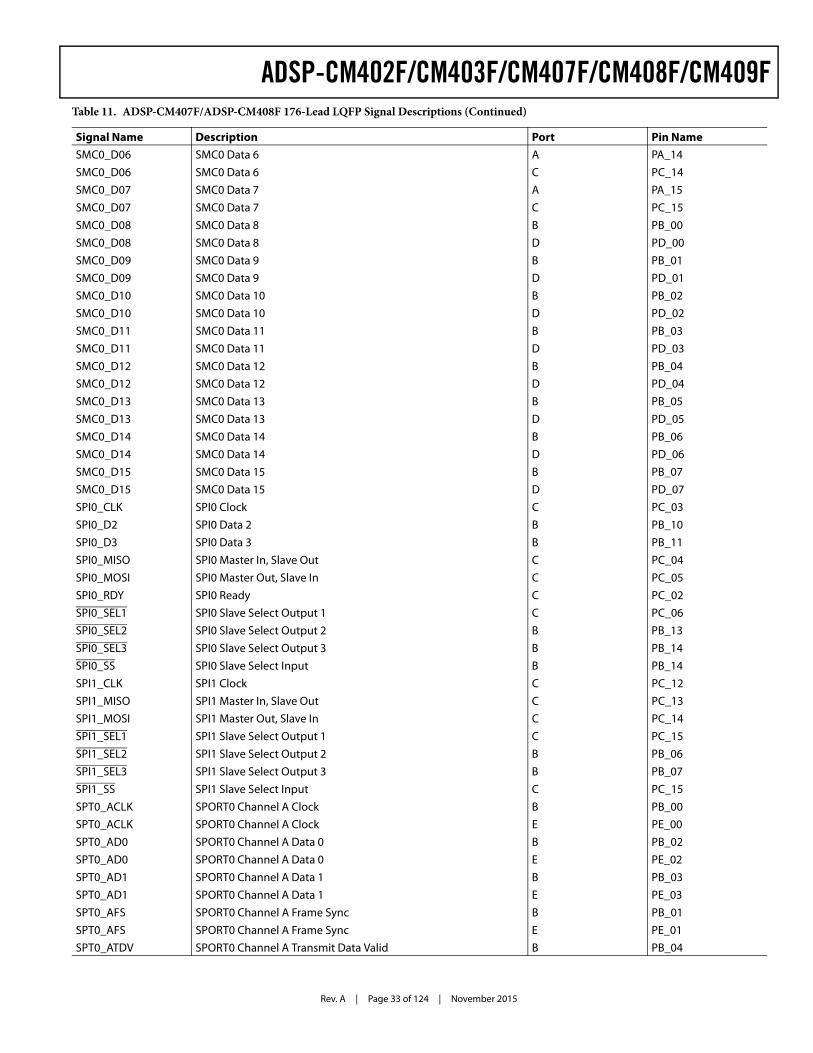
Rev. A | Page 33 of 124 | November 2015
ADSP-CM402F/CM403F/CM407F/CM408F/CM409F
SMC0_D06 SMC0 Data 6 A PA_14SMC0_D06 SMC0 Data 6 C PC_14SMC0_D07 SMC0 Data 7 A PA_15SMC0_D07 SMC0 Data 7 C PC_15SMC0_D08 SMC0 Data 8 B PB_00SMC0_D08 SMC0 Data 8 D PD_00SMC0_D09 SMC0 Data 9 B PB_01SMC0_D09 SMC0 Data 9 D PD_01SMC0_D10 SMC0 Data 10 B PB_02SMC0_D10 SMC0 Data 10 D PD_02SMC0_D11 SMC0 Data 11 B PB_03SMC0_D11 SMC0 Data 11 D PD_03SMC0_D12 SMC0 Data 12 B PB_04SMC0_D12 SMC0 Data 12 D PD_04SMC0_D13 SMC0 Data 13 B PB_05SMC0_D13 SMC0 Data 13 D PD_05SMC0_D14 SMC0 Data 14 B PB_06SMC0_D14 SMC0 Data 14 D PD_06SMC0_D15 SMC0 Data 15 B PB_07SMC0_D15 SMC0 Data 15 D PD_07SPI0_CLK SPI0 Clock C PC_03SPI0_D2 SPI0 Data 2 B PB_10SPI0_D3 SPI0 Data 3 B PB_11SPI0_MISO SPI0 Master In, Slave Out C PC_04SPI0_MOSI SPI0 Master Out, Slave In C PC_05SPI0_RDY SPI0 Ready C PC_02SPI0_SEL1 SPI0 Slave Select Output 1 C PC_06SPI0_SEL2 SPI0 Slave Select Output 2 B PB_13SPI0_SEL3 SPI0 Slave Select Output 3 B PB_14SPI0_SS SPI0 Slave Select Input B PB_14SPI1_CLK SPI1 Clock C PC_12SPI1_MISO SPI1 Master In, Slave Out C PC_13SPI1_MOSI SPI1 Master Out, Slave In C PC_14SPI1_SEL1 SPI1 Slave Select Output 1 C PC_15SPI1_SEL2 SPI1 Slave Select Output 2 B PB_06SPI1_SEL3 SPI1 Slave Select Output 3 B PB_07SPI1_SS SPI1 Slave Select Input C PC_15SPT0_ACLK SPORT0 Channel A Clock B PB_00SPT0_ACLK SPORT0 Channel A Clock E PE_00SPT0_AD0 SPORT0 Channel A Data 0 B PB_02SPT0_AD0 SPORT0 Channel A Data 0 E PE_02SPT0_AD1 SPORT0 Channel A Data 1 B PB_03SPT0_AD1 SPORT0 Channel A Data 1 E PE_03SPT0_AFS SPORT0 Channel A Frame Sync B PB_01SPT0_AFS SPORT0 Channel A Frame Sync E PE_01SPT0_ATDV SPORT0 Channel A Transmit Data Valid B PB_04
Table 11. ADSP-CM407F/ADSP-CM408F 176-Lead LQFP Signal Descriptions (Continued)
Signal Name Description Port Pin Name
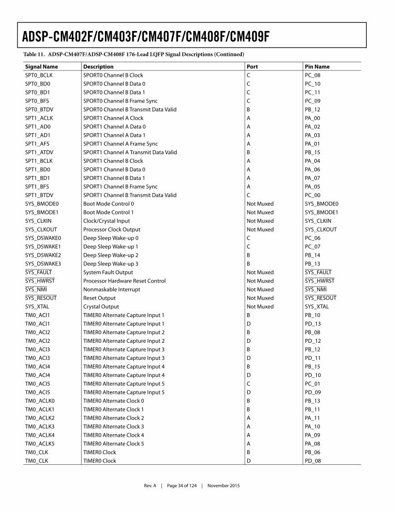
Rev. A | Page 34 of 124 | November 2015
ADSP-CM402F/CM403F/CM407F/CM408F/CM409F
SPT0_BCLK SPORT0 Channel B Clock C PC_08SPT0_BD0 SPORT0 Channel B Data 0 C PC_10SPT0_BD1 SPORT0 Channel B Data 1 C PC_11SPT0_BFS SPORT0 Channel B Frame Sync C PC_09SPT0_BTDV SPORT0 Channel B Transmit Data Valid B PB_12SPT1_ACLK SPORT1 Channel A Clock A PA_00SPT1_AD0 SPORT1 Channel A Data 0 A PA_02SPT1_AD1 SPORT1 Channel A Data 1 A PA_03SPT1_AFS SPORT1 Channel A Frame Sync A PA_01SPT1_ATDV SPORT1 Channel A Transmit Data Valid B PB_15SPT1_BCLK SPORT1 Channel B Clock A PA_04SPT1_BD0 SPORT1 Channel B Data 0 A PA_06SPT1_BD1 SPORT1 Channel B Data 1 A PA_07SPT1_BFS SPORT1 Channel B Frame Sync A PA_05SPT1_BTDV SPORT1 Channel B Transmit Data Valid C PC_00SYS_BMODE0 Boot Mode Control 0 Not Muxed SYS_BMODE0SYS_BMODE1 Boot Mode Control 1 Not Muxed SYS_BMODE1SYS_CLKIN Clock/Crystal Input Not Muxed SYS_CLKINSYS_CLKOUT Processor Clock Output Not Muxed SYS_CLKOUTSYS_DSWAKE0 Deep Sleep Wake-up 0 C PC_06SYS_DSWAKE1 Deep Sleep Wake-up 1 C PC_07SYS_DSWAKE2 Deep Sleep Wake-up 2 B PB_14SYS_DSWAKE3 Deep Sleep Wake-up 3 B PB_13SYS_FAULT System Fault Output Not Muxed SYS_FAULTSYS_HWRST Processor Hardware Reset Control Not Muxed SYS_HWRSTSYS_NMI Nonmaskable Interrupt Not Muxed SYS_NMISYS_RESOUT Reset Output Not Muxed SYS_RESOUTSYS_XTAL Crystal Output Not Muxed SYS_XTALTM0_ACI1 TIMER0 Alternate Capture Input 1 B PB_10TM0_ACI1 TIMER0 Alternate Capture Input 1 D PD_13TM0_ACI2 TIMER0 Alternate Capture Input 2 B PB_08TM0_ACI2 TIMER0 Alternate Capture Input 2 D PD_12TM0_ACI3 TIMER0 Alternate Capture Input 3 B PB_12TM0_ACI3 TIMER0 Alternate Capture Input 3 D PD_11TM0_ACI4 TIMER0 Alternate Capture Input 4 B PB_15TM0_ACI4 TIMER0 Alternate Capture Input 4 D PD_10TM0_ACI5 TIMER0 Alternate Capture Input 5 C PC_01TM0_ACI5 TIMER0 Alternate Capture Input 5 D PD_09TM0_ACLK0 TIMER0 Alternate Clock 0 B PB_13TM0_ACLK1 TIMER0 Alternate Clock 1 B PB_11TM0_ACLK2 TIMER0 Alternate Clock 2 A PA_11TM0_ACLK3 TIMER0 Alternate Clock 3 A PA_10TM0_ACLK4 TIMER0 Alternate Clock 4 A PA_09TM0_ACLK5 TIMER0 Alternate Clock 5 A PA_08TM0_CLK TIMER0 Clock B PB_06TM0_CLK TIMER0 Clock D PD_08
Table 11. ADSP-CM407F/ADSP-CM408F 176-Lead LQFP Signal Descriptions (Continued)
Signal Name Description Port Pin Name
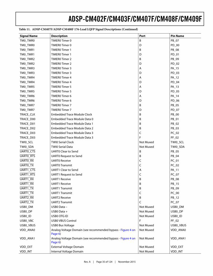
Rev. A | Page 35 of 124 | November 2015
ADSP-CM402F/CM403F/CM407F/CM408F/CM409F
TM0_TMR0 TIMER0 Timer 0 B PB_07TM0_TMR0 TIMER0 Timer 0 D PD_00TM0_TMR1 TIMER0 Timer 1 B PB_08TM0_TMR1 TIMER0 Timer 1 D PD_01TM0_TMR2 TIMER0 Timer 2 B PB_09TM0_TMR2 TIMER0 Timer 2 D PD_02TM0_TMR3 TIMER0 Timer 3 A PA_15TM0_TMR3 TIMER0 Timer 3 D PD_03TM0_TMR4 TIMER0 Timer 4 A PA_12TM0_TMR4 TIMER0 Timer 4 D PD_04TM0_TMR5 TIMER0 Timer 5 A PA_13TM0_TMR5 TIMER0 Timer 5 D PD_05TM0_TMR6 TIMER0 Timer 6 A PA_14TM0_TMR6 TIMER0 Timer 6 D PD_06TM0_TMR7 TIMER0 Timer 7 B PB_05TM0_TMR7 TIMER0 Timer 7 D PD_07TRACE_CLK Embedded Trace Module Clock B PB_00TRACE_D00 Embedded Trace Module Data 0 B PB_01TRACE_D01 Embedded Trace Module Data 1 B PB_02TRACE_D02 Embedded Trace Module Data 2 B PB_03TRACE_D03 Embedded Trace Module Data 3 C PC_02TRACE_D03 Embedded Trace Module Data 3 F PF_02TWI0_SCL TWI0 Serial Clock Not Muxed TWI0_SCLTWI0_SDA TWI0 Serial Data Not Muxed TWI0_SDAUART0_CTS UART0 Clear to Send B PB_05UART0_RTS UART0 Request to Send B PB_04UART0_RX UART0 Receive C PC_01UART0_TX UART0 Transmit C PC_02UART1_CTS UART1 Clear to Send A PA_11UART1_RTS UART1 Request to Send C PC_07UART1_RX UART1 Receive B PB_08UART1_RX UART1 Receive B PB_15UART1_TX UART1 Transmit B PB_09UART1_TX UART1 Transmit C PC_00UART2_RX UART2 Receive B PB_12UART2_TX UART2 Transmit C PC_07USB0_DM USB0 Data – Not Muxed USB0_DMUSB0_DP USB0 Data + Not Muxed USB0_DPUSB0_ID USB0 OTG ID Not Muxed USB0_IDUSB0_VBC USB0 VBUS Control F PF_02USB0_VBUS USB0 Bus Voltage Not Muxed USB0_VBUSVDD_ANA0 Analog Voltage Domain (see recommended bypass - Figure 4 on
Page 6)Not Muxed VDD_ANA0
VDD_ANA1 Analog Voltage Domain (see recommended bypass - Figure 4 on Page 6)
Not Muxed VDD_ANA1
VDD_EXT External Voltage Domain Not Muxed VDD_EXTVDD_INT Internal Voltage Domain Not Muxed VDD_INT
Table 11. ADSP-CM407F/ADSP-CM408F 176-Lead LQFP Signal Descriptions (Continued)
Signal Name Description Port Pin Name
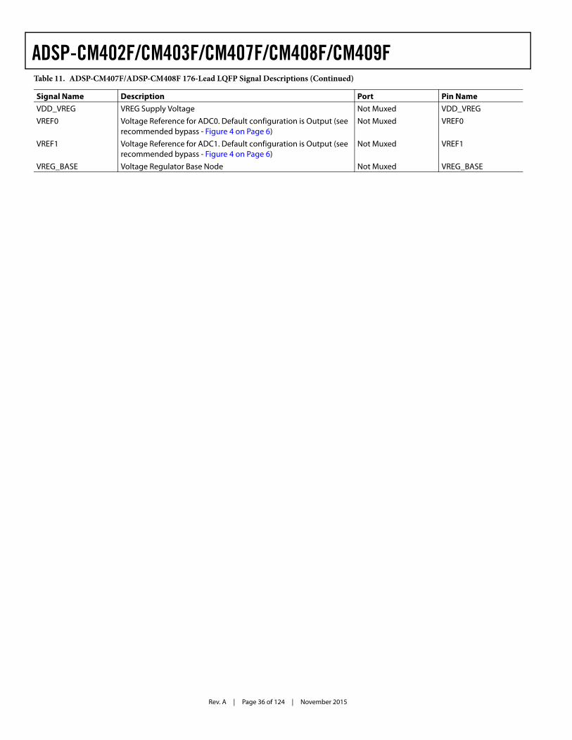
Rev. A | Page 36 of 124 | November 2015
ADSP-CM402F/CM403F/CM407F/CM408F/CM409F
VDD_VREG VREG Supply Voltage Not Muxed VDD_VREGVREF0 Voltage Reference for ADC0. Default configuration is Output (see
recommended bypass - Figure 4 on Page 6)Not Muxed VREF0
VREF1 Voltage Reference for ADC1. Default configuration is Output (see recommended bypass - Figure 4 on Page 6)
Not Muxed VREF1
VREG_BASE Voltage Regulator Base Node Not Muxed VREG_BASE
Table 11. ADSP-CM407F/ADSP-CM408F 176-Lead LQFP Signal Descriptions (Continued)
Signal Name Description Port Pin Name
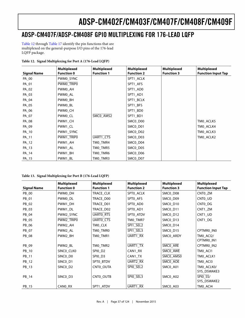
Rev. A | Page 37 of 124 | November 2015
ADSP-CM402F/CM403F/CM407F/CM408F/CM409FADSP-CM407F/ADSP-CM408F GPIO MULTIPLEXING FOR 176-LEAD LQFPTable 12 through Table 17 identify the pin functions that are multiplexed on the general-purpose I/O pins of the 176-lead LQFP package.
Table 12. Signal Multiplexing for Port A (176-Lead LQFP)
Signal NameMultiplexed Function 0
Multiplexed Function 1
Multiplexed Function 2
Multiplexed Function 3
Multiplexed Function Input Tap
PA_00 PWM0_SYNC SPT1_ACLKPA_01 PWM0_TRIP0 SPT1_AFSPA_02 PWM0_AH SPT1_AD0PA_03 PWM0_AL SPT1_AD1PA_04 PWM0_BH SPT1_BCLKPA_05 PWM0_BL SPT1_BFSPA_06 PWM0_CH SPT1_BD0PA_07 PWM0_CL SMC0_AMS2 SPT1_BD1PA_08 PWM1_CH SMC0_D00 TM0_ACLK5PA_09 PWM1_CL SMC0_D01 TM0_ACLK4PA_10 PWM1_SYNC SMC0_D02 TM0_ACLK3PA_11 PWM1_TRIP0 UART1_CTS SMC0_D03 TM0_ACLK2PA_12 PWM1_AH TM0_TMR4 SMC0_D04PA_13 PWM1_AL TM0_TMR5 SMC0_D05PA_14 PWM1_BH TM0_TMR6 SMC0_D06PA_15 PWM1_BL TM0_TMR3 SMC0_D07
Table 13. Signal Multiplexing for Port B (176-Lead LQFP)
Signal NameMultiplexed Function 0
Multiplexed Function 1
Multiplexed Function 2
Multiplexed Function 3
Multiplexed Function Input Tap
PB_00 PWM0_DH TRACE_CLK SPT0_ACLK SMC0_D08 CNT0_ZMPB_01 PWM0_DL TRACE_D00 SPT0_AFS SMC0_D09 CNT0_UDPB_02 PWM1_DH TRACE_D01 SPT0_AD0 SMC0_D10 CNT0_DGPB_03 PWM1_DL TRACE_D02 SPT0_AD1 SMC0_D11 CNT1_ZMPB_04 PWM2_SYNC UART0_RTS SPT0_ATDV SMC0_D12 CNT1_UDPB_05 PWM2_TRIP0 UART0_CTS TM0_TMR7 SMC0_D13 CNT1_DGPB_06 PWM2_AH TM0_CLK SPI1_SEL2 SMC0_D14PB_07 PWM2_AL TM0_TMR0 SPI1_SEL3 SMC0_D15 CPTMR0_IN0PB_08 PWM2_BH TM0_TMR1 UART1_RX SMC0_ARDY TM0_ACI2/
CPTMR0_IN1PB_09 PWM2_BL TM0_TMR2 UART1_TX SMC0_ARE CPTMR0_IN2PB_10 SINC0_CLK0 SPI0_D2 CAN1_RX SMC0_AWE TM0_ACI1PB_11 SINC0_D0 SPI0_D3 CAN1_TX SMC0_AMS0 TM0_ACLK1PB_12 SINC0_D1 SPT0_BTDV UART2_RX SMC0_AOE TM0_ACI3PB_13 SINC0_D2 CNT0_OUTA SPI0_SEL2 SMC0_A01 TM0_ACLK0/
SYS_DSWAKE3PB_14 SINC0_D3 CNT0_OUTB SPI0_SEL3 SMC0_A02 SPI0_SS/
SYS_DSWAKE2PB_15 CAN0_RX SPT1_ATDV UART1_RX SMC0_A03 TM0_ACI4
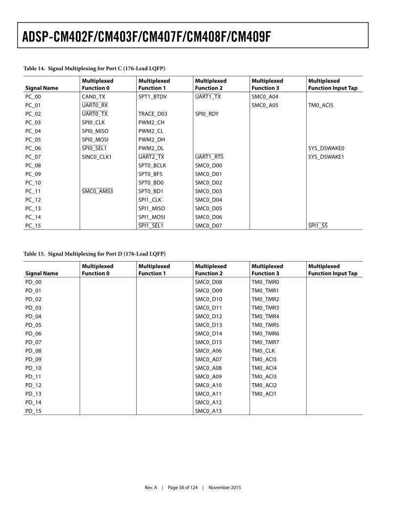
Rev. A | Page 38 of 124 | November 2015
ADSP-CM402F/CM403F/CM407F/CM408F/CM409F
Table 14. Signal Multiplexing for Port C (176-Lead LQFP)
Signal NameMultiplexed Function 0
Multiplexed Function 1
Multiplexed Function 2
Multiplexed Function 3
Multiplexed Function Input Tap
PC_00 CAN0_TX SPT1_BTDV UART1_TX SMC0_A04PC_01 UART0_RX SMC0_A05 TM0_ACI5PC_02 UART0_TX TRACE_D03 SPI0_RDYPC_03 SPI0_CLK PWM2_CHPC_04 SPI0_MISO PWM2_CLPC_05 SPI0_MOSI PWM2_DHPC_06 SPI0_SEL1 PWM2_DL SYS_DSWAKE0PC_07 SINC0_CLK1 UART2_TX UART1_RTS SYS_DSWAKE1PC_08 SPT0_BCLK SMC0_D00PC_09 SPT0_BFS SMC0_D01PC_10 SPT0_BD0 SMC0_D02PC_11 SMC0_AMS3 SPT0_BD1 SMC0_D03PC_12 SPI1_CLK SMC0_D04PC_13 SPI1_MISO SMC0_D05PC_14 SPI1_MOSI SMC0_D06PC_15 SPI1_SEL1 SMC0_D07 SPI1_SS
Table 15. Signal Multiplexing for Port D (176-Lead LQFP)
Signal NameMultiplexed Function 0
Multiplexed Function 1
Multiplexed Function 2
Multiplexed Function 3
Multiplexed Function Input Tap
PD_00 SMC0_D08 TM0_TMR0PD_01 SMC0_D09 TM0_TMR1PD_02 SMC0_D10 TM0_TMR2PD_03 SMC0_D11 TM0_TMR3PD_04 SMC0_D12 TM0_TMR4PD_05 SMC0_D13 TM0_TMR5PD_06 SMC0_D14 TM0_TMR6PD_07 SMC0_D15 TM0_TMR7PD_08 SMC0_A06 TM0_CLKPD_09 SMC0_A07 TM0_ACI5PD_10 SMC0_A08 TM0_ACI4PD_11 SMC0_A09 TM0_ACI3PD_12 SMC0_A10 TM0_ACI2PD_13 SMC0_A11 TM0_ACI1PD_14 SMC0_A12PD_15 SMC0_A13
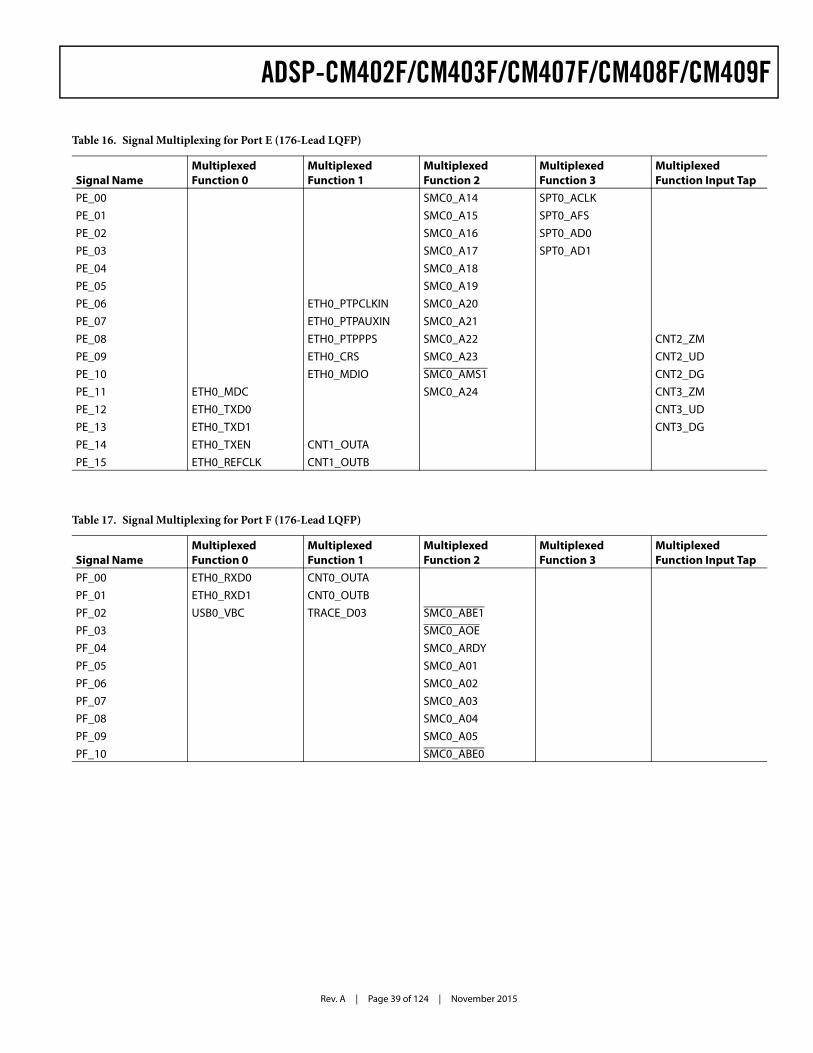
Rev. A | Page 39 of 124 | November 2015
ADSP-CM402F/CM403F/CM407F/CM408F/CM409F
Table 16. Signal Multiplexing for Port E (176-Lead LQFP)
Signal NameMultiplexed Function 0
Multiplexed Function 1
Multiplexed Function 2
Multiplexed Function 3
Multiplexed Function Input Tap
PE_00 SMC0_A14 SPT0_ACLKPE_01 SMC0_A15 SPT0_AFSPE_02 SMC0_A16 SPT0_AD0PE_03 SMC0_A17 SPT0_AD1PE_04 SMC0_A18PE_05 SMC0_A19PE_06 ETH0_PTPCLKIN SMC0_A20PE_07 ETH0_PTPAUXIN SMC0_A21PE_08 ETH0_PTPPPS SMC0_A22 CNT2_ZMPE_09 ETH0_CRS SMC0_A23 CNT2_UDPE_10 ETH0_MDIO SMC0_AMS1 CNT2_DGPE_11 ETH0_MDC SMC0_A24 CNT3_ZMPE_12 ETH0_TXD0 CNT3_UDPE_13 ETH0_TXD1 CNT3_DGPE_14 ETH0_TXEN CNT1_OUTAPE_15 ETH0_REFCLK CNT1_OUTB
Table 17. Signal Multiplexing for Port F (176-Lead LQFP)
Signal NameMultiplexed Function 0
Multiplexed Function 1
Multiplexed Function 2
Multiplexed Function 3
Multiplexed Function Input Tap
PF_00 ETH0_RXD0 CNT0_OUTAPF_01 ETH0_RXD1 CNT0_OUTBPF_02 USB0_VBC TRACE_D03 SMC0_ABE1PF_03 SMC0_AOEPF_04 SMC0_ARDYPF_05 SMC0_A01PF_06 SMC0_A02PF_07 SMC0_A03PF_08 SMC0_A04PF_09 SMC0_A05PF_10 SMC0_ABE0
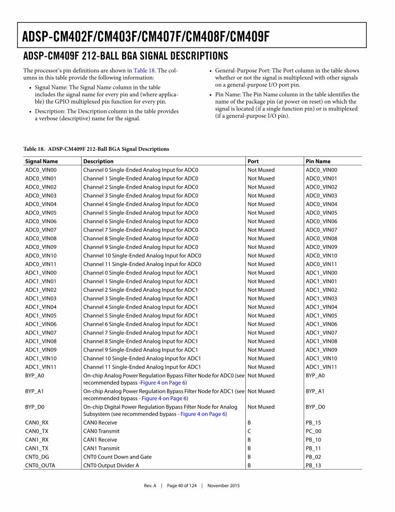
Rev. A | Page 40 of 124 | November 2015
ADSP-CM402F/CM403F/CM407F/CM408F/CM409FADSP-CM409F 212-BALL BGA SIGNAL DESCRIPTIONSThe processor’s pin definitions are shown in Table 18. The col-umns in this table provide the following information:
• Signal Name: The Signal Name column in the table includes the signal name for every pin and (where applica-ble) the GPIO multiplexed pin function for every pin.
• Description: The Description column in the table provides a verbose (descriptive) name for the signal.
• General-Purpose Port: The Port column in the table shows whether or not the signal is multiplexed with other signals on a general-purpose I/O port pin.
• Pin Name: The Pin Name column in the table identifies the name of the package pin (at power on reset) on which the signal is located (if a single function pin) or is multiplexed (if a general-purpose I/O pin).
Table 18. ADSP-CM409F 212-Ball BGA Signal Descriptions
Signal Name Description Port Pin NameADC0_VIN00 Channel 0 Single-Ended Analog Input for ADC0 Not Muxed ADC0_VIN00ADC0_VIN01 Channel 1 Single-Ended Analog Input for ADC0 Not Muxed ADC0_VIN01ADC0_VIN02 Channel 2 Single-Ended Analog Input for ADC0 Not Muxed ADC0_VIN02ADC0_VIN03 Channel 3 Single-Ended Analog Input for ADC0 Not Muxed ADC0_VIN03ADC0_VIN04 Channel 4 Single-Ended Analog Input for ADC0 Not Muxed ADC0_VIN04ADC0_VIN05 Channel 5 Single-Ended Analog Input for ADC0 Not Muxed ADC0_VIN05ADC0_VIN06 Channel 6 Single-Ended Analog Input for ADC0 Not Muxed ADC0_VIN06ADC0_VIN07 Channel 7 Single-Ended Analog Input for ADC0 Not Muxed ADC0_VIN07ADC0_VIN08 Channel 8 Single-Ended Analog Input for ADC0 Not Muxed ADC0_VIN08ADC0_VIN09 Channel 9 Single-Ended Analog Input for ADC0 Not Muxed ADC0_VIN09ADC0_VIN10 Channel 10 Single-Ended Analog Input for ADC0 Not Muxed ADC0_VIN10ADC0_VIN11 Channel 11 Single-Ended Analog Input for ADC0 Not Muxed ADC0_VIN11ADC1_VIN00 Channel 0 Single-Ended Analog Input for ADC1 Not Muxed ADC1_VIN00ADC1_VIN01 Channel 1 Single-Ended Analog Input for ADC1 Not Muxed ADC1_VIN01ADC1_VIN02 Channel 2 Single-Ended Analog Input for ADC1 Not Muxed ADC1_VIN02ADC1_VIN03 Channel 3 Single-Ended Analog Input for ADC1 Not Muxed ADC1_VIN03ADC1_VIN04 Channel 4 Single-Ended Analog Input for ADC1 Not Muxed ADC1_VIN04ADC1_VIN05 Channel 5 Single-Ended Analog Input for ADC1 Not Muxed ADC1_VIN05ADC1_VIN06 Channel 6 Single-Ended Analog Input for ADC1 Not Muxed ADC1_VIN06ADC1_VIN07 Channel 7 Single-Ended Analog Input for ADC1 Not Muxed ADC1_VIN07ADC1_VIN08 Channel 8 Single-Ended Analog Input for ADC1 Not Muxed ADC1_VIN08ADC1_VIN09 Channel 9 Single-Ended Analog Input for ADC1 Not Muxed ADC1_VIN09ADC1_VIN10 Channel 10 Single-Ended Analog Input for ADC1 Not Muxed ADC1_VIN10ADC1_VIN11 Channel 11 Single-Ended Analog Input for ADC1 Not Muxed ADC1_VIN11BYP_A0 On-chip Analog Power Regulation Bypass Filter Node for ADC0 (see
recommended bypass -Figure 4 on Page 6)Not Muxed BYP_A0
BYP_A1 On-chip Analog Power Regulation Bypass Filter Node for ADC1 (see recommended bypass - Figure 4 on Page 6)
Not Muxed BYP_A1
BYP_D0 On-chip Digital Power Regulation Bypass Filter Node for Analog Subsystem (see recommended bypass - Figure 4 on Page 6)
Not Muxed BYP_D0
CAN0_RX CAN0 Receive B PB_15CAN0_TX CAN0 Transmit C PC_00CAN1_RX CAN1 Receive B PB_10CAN1_TX CAN1 Transmit B PB_11CNT0_DG CNT0 Count Down and Gate B PB_02CNT0_OUTA CNT0 Output Divider A B PB_13
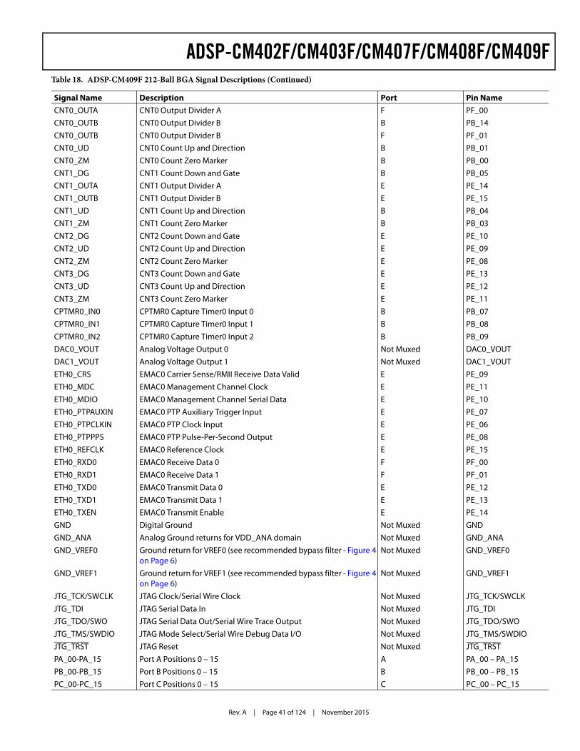
Rev. A | Page 41 of 124 | November 2015
ADSP-CM402F/CM403F/CM407F/CM408F/CM409F
CNT0_OUTA CNT0 Output Divider A F PF_00CNT0_OUTB CNT0 Output Divider B B PB_14CNT0_OUTB CNT0 Output Divider B F PF_01CNT0_UD CNT0 Count Up and Direction B PB_01CNT0_ZM CNT0 Count Zero Marker B PB_00CNT1_DG CNT1 Count Down and Gate B PB_05CNT1_OUTA CNT1 Output Divider A E PE_14CNT1_OUTB CNT1 Output Divider B E PE_15CNT1_UD CNT1 Count Up and Direction B PB_04CNT1_ZM CNT1 Count Zero Marker B PB_03CNT2_DG CNT2 Count Down and Gate E PE_10CNT2_UD CNT2 Count Up and Direction E PE_09CNT2_ZM CNT2 Count Zero Marker E PE_08CNT3_DG CNT3 Count Down and Gate E PE_13CNT3_UD CNT3 Count Up and Direction E PE_12CNT3_ZM CNT3 Count Zero Marker E PE_11CPTMR0_IN0 CPTMR0 Capture Timer0 Input 0 B PB_07CPTMR0_IN1 CPTMR0 Capture Timer0 Input 1 B PB_08CPTMR0_IN2 CPTMR0 Capture Timer0 Input 2 B PB_09DAC0_VOUT Analog Voltage Output 0 Not Muxed DAC0_VOUTDAC1_VOUT Analog Voltage Output 1 Not Muxed DAC1_VOUTETH0_CRS EMAC0 Carrier Sense/RMII Receive Data Valid E PE_09ETH0_MDC EMAC0 Management Channel Clock E PE_11ETH0_MDIO EMAC0 Management Channel Serial Data E PE_10ETH0_PTPAUXIN EMAC0 PTP Auxiliary Trigger Input E PE_07ETH0_PTPCLKIN EMAC0 PTP Clock Input E PE_06ETH0_PTPPPS EMAC0 PTP Pulse-Per-Second Output E PE_08ETH0_REFCLK EMAC0 Reference Clock E PE_15ETH0_RXD0 EMAC0 Receive Data 0 F PF_00ETH0_RXD1 EMAC0 Receive Data 1 F PF_01ETH0_TXD0 EMAC0 Transmit Data 0 E PE_12ETH0_TXD1 EMAC0 Transmit Data 1 E PE_13ETH0_TXEN EMAC0 Transmit Enable E PE_14GND Digital Ground Not Muxed GNDGND_ANA Analog Ground returns for VDD_ANA domain Not Muxed GND_ANAGND_VREF0 Ground return for VREF0 (see recommended bypass filter - Figure 4
on Page 6)Not Muxed GND_VREF0
GND_VREF1 Ground return for VREF1 (see recommended bypass filter - Figure 4 on Page 6)
Not Muxed GND_VREF1
JTG_TCK/SWCLK JTAG Clock/Serial Wire Clock Not Muxed JTG_TCK/SWCLKJTG_TDI JTAG Serial Data In Not Muxed JTG_TDIJTG_TDO/SWO JTAG Serial Data Out/Serial Wire Trace Output Not Muxed JTG_TDO/SWOJTG_TMS/SWDIO JTAG Mode Select/Serial Wire Debug Data I/O Not Muxed JTG_TMS/SWDIOJTG_TRST JTAG Reset Not Muxed JTG_TRSTPA_00-PA_15 Port A Positions 0 – 15 A PA_00 – PA_15PB_00-PB_15 Port B Positions 0 – 15 B PB_00 – PB_15PC_00-PC_15 Port C Positions 0 – 15 C PC_00 – PC_15
Table 18. ADSP-CM409F 212-Ball BGA Signal Descriptions (Continued)
Signal Name Description Port Pin Name
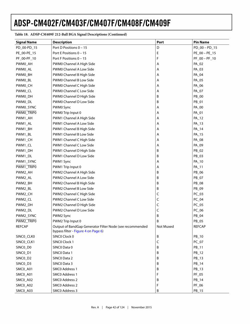
Rev. A | Page 42 of 124 | November 2015
ADSP-CM402F/CM403F/CM407F/CM408F/CM409F
PD_00-PD_15 Port D Positions 0 – 15 D PD_00 – PD_15PE_00-PE_15 Port E Positions 0 – 15 E PE_00 – PE_15PF_00-PF_10 Port F Positions 0 – 15 F PF_00 – PF_10PWM0_AH PWM0 Channel A High Side A PA_02PWM0_AL PWM0 Channel A Low Side A PA_03PWM0_BH PWM0 Channel B High Side A PA_04PWM0_BL PWM0 Channel B Low Side A PA_05PWM0_CH PWM0 Channel C High Side A PA_06PWM0_CL PWM0 Channel C Low Side A PA_07PWM0_DH PWM0 Channel D High Side B PB_00PWM0_DL PWM0 Channel D Low Side B PB_01PWM0_SYNC PWM0 Sync A PA_00PWM0_TRIP0 PWM0 Trip Input 0 A PA_01PWM1_AH PWM1 Channel A High Side A PA_12PWM1_AL PWM1 Channel A Low Side A PA_13PWM1_BH PWM1 Channel B High Side A PA_14PWM1_BL PWM1 Channel B Low Side A PA_15PWM1_CH PWM1 Channel C High Side A PA_08PWM1_CL PWM1 Channel C Low Side A PA_09PWM1_DH PWM1 Channel D High Side B PB_02PWM1_DL PWM1 Channel D Low Side B PB_03PWM1_SYNC PWM1 Sync A PA_10PWM1_TRIP0 PWM1 Trip Input 0 A PA_11PWM2_AH PWM2 Channel A High Side B PB_06PWM2_AL PWM2 Channel A Low Side B PB_07PWM2_BH PWM2 Channel B High Side B PB_08PWM2_BL PWM2 Channel B Low Side B PB_09PWM2_CH PWM2 Channel C High Side C PC_03PWM2_CL PWM2 Channel C Low Side C PC_04PWM2_DH PWM2 Channel D High Side C PC_05PWM2_DL PWM2 Channel D Low Side C PC_06PWM2_SYNC PWM2 Sync B PB_04PWM2_TRIP0 PWM2 Trip Input 0 B PB_05REFCAP Output of BandGap Generator Filter Node (see recommended
bypass filter - Figure 4 on Page 6)Not Muxed REFCAP
SINC0_CLK0 SINC0 Clock 0 B PB_10SINC0_CLK1 SINC0 Clock 1 C PC_07SINC0_D0 SINC0 Data 0 B PB_11SINC0_D1 SINC0 Data 1 B PB_12SINC0_D2 SINC0 Data 2 B PB_13SINC0_D3 SINC0 Data 3 B PB_14SMC0_A01 SMC0 Address 1 B PB_13SMC0_A01 SMC0 Address 1 F PF_05SMC0_A02 SMC0 Address 2 B PB_14SMC0_A02 SMC0 Address 2 F PF_06SMC0_A03 SMC0 Address 3 B PB_15
Table 18. ADSP-CM409F 212-Ball BGA Signal Descriptions (Continued)
Signal Name Description Port Pin Name
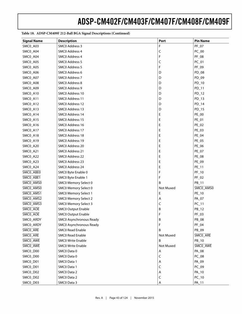
Rev. A | Page 43 of 124 | November 2015
ADSP-CM402F/CM403F/CM407F/CM408F/CM409F
SMC0_A03 SMC0 Address 3 F PF_07SMC0_A04 SMC0 Address 4 C PC_00SMC0_A04 SMC0 Address 4 F PF_08SMC0_A05 SMC0 Address 5 C PC_01SMC0_A05 SMC0 Address 5 F PF_09SMC0_A06 SMC0 Address 6 D PD_08SMC0_A07 SMC0 Address 7 D PD_09SMC0_A08 SMC0 Address 8 D PD_10SMC0_A09 SMC0 Address 9 D PD_11SMC0_A10 SMC0 Address 10 D PD_12SMC0_A11 SMC0 Address 11 D PD_13SMC0_A12 SMC0 Address 12 D PD_14SMC0_A13 SMC0 Address 13 D PD_15SMC0_A14 SMC0 Address 14 E PE_00SMC0_A15 SMC0 Address 15 E PE_01SMC0_A16 SMC0 Address 16 E PE_02SMC0_A17 SMC0 Address 17 E PE_03SMC0_A18 SMC0 Address 18 E PE_04SMC0_A19 SMC0 Address 19 E PE_05SMC0_A20 SMC0 Address 20 E PE_06SMC0_A21 SMC0 Address 21 E PE_07SMC0_A22 SMC0 Address 22 E PE_08SMC0_A23 SMC0 Address 23 E PE_09SMC0_A24 SMC0 Address 24 E PE_11SMC0_ABE0 SMC0 Byte Enable 0 F PF_10SMC0_ABE1 SMC0 Byte Enable 1 F PF_02SMC0_AMS0 SMC0 Memory Select 0 B PB_11SMC0_AMS0 SMC0 Memory Select 0 Not Muxed SMC0_AMS0SMC0_AMS1 SMC0 Memory Select 1 E PE_10SMC0_AMS2 SMC0 Memory Select 2 A PA_07SMC0_AMS3 SMC0 Memory Select 3 C PC_11SMC0_AOE SMC0 Output Enable B PB_12SMC0_AOE SMC0 Output Enable F PF_03SMC0_ARDY SMC0 Asynchronous Ready B PB_08SMC0_ARDY SMC0 Asynchronous Ready F PF_04SMC0_ARE SMC0 Read Enable B PB_09SMC0_ARE SMC0 Read Enable Not Muxed SMC0_ARESMC0_AWE SMC0 Write Enable B PB_10SMC0_AWE SMC0 Write Enable Not Muxed SMC0_AWESMC0_D00 SMC0 Data 0 A PA_08SMC0_D00 SMC0 Data 0 C PC_08SMC0_D01 SMC0 Data 1 A PA_09SMC0_D01 SMC0 Data 1 C PC_09SMC0_D02 SMC0 Data 2 A PA_10SMC0_D02 SMC0 Data 2 C PC_10SMC0_D03 SMC0 Data 3 A PA_11
Table 18. ADSP-CM409F 212-Ball BGA Signal Descriptions (Continued)
Signal Name Description Port Pin Name
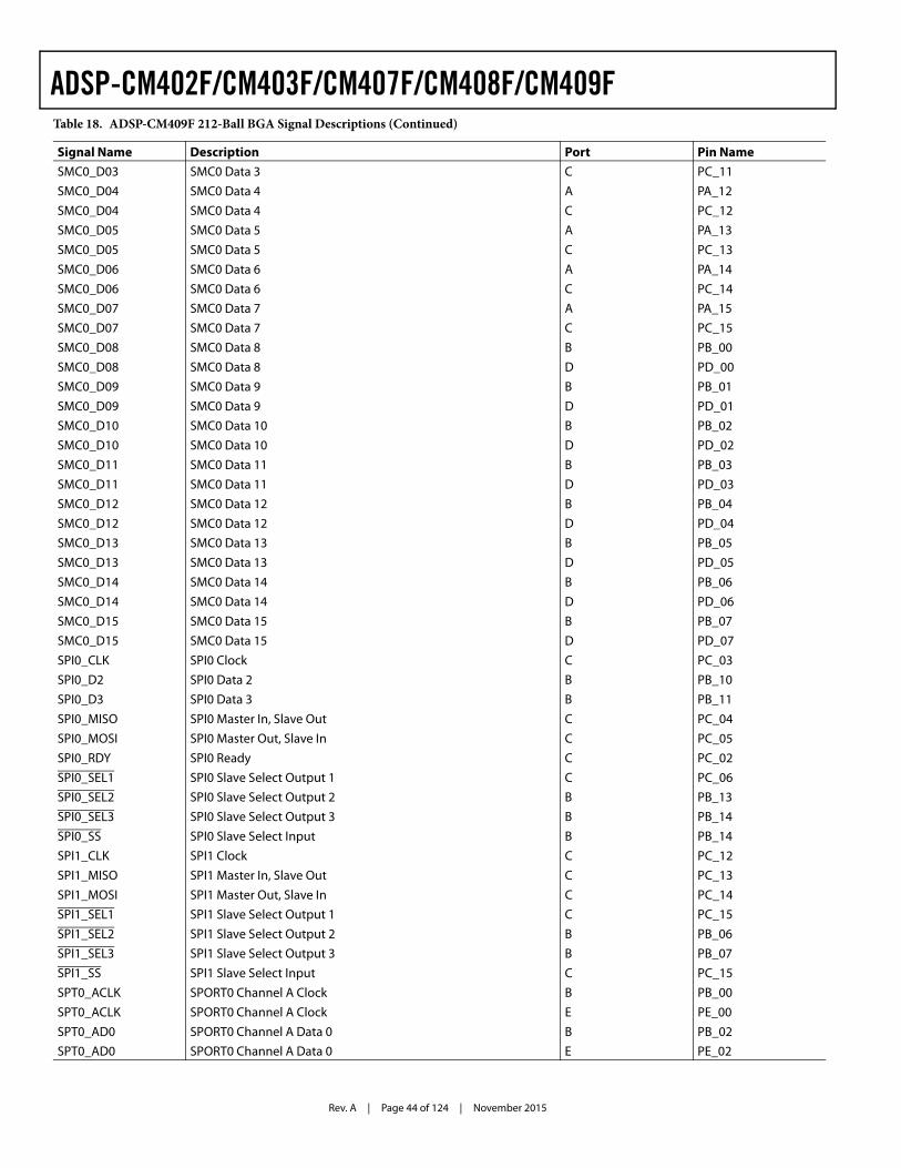
Rev. A | Page 44 of 124 | November 2015
ADSP-CM402F/CM403F/CM407F/CM408F/CM409F
SMC0_D03 SMC0 Data 3 C PC_11SMC0_D04 SMC0 Data 4 A PA_12SMC0_D04 SMC0 Data 4 C PC_12SMC0_D05 SMC0 Data 5 A PA_13SMC0_D05 SMC0 Data 5 C PC_13SMC0_D06 SMC0 Data 6 A PA_14SMC0_D06 SMC0 Data 6 C PC_14SMC0_D07 SMC0 Data 7 A PA_15SMC0_D07 SMC0 Data 7 C PC_15SMC0_D08 SMC0 Data 8 B PB_00SMC0_D08 SMC0 Data 8 D PD_00SMC0_D09 SMC0 Data 9 B PB_01SMC0_D09 SMC0 Data 9 D PD_01SMC0_D10 SMC0 Data 10 B PB_02SMC0_D10 SMC0 Data 10 D PD_02SMC0_D11 SMC0 Data 11 B PB_03SMC0_D11 SMC0 Data 11 D PD_03SMC0_D12 SMC0 Data 12 B PB_04SMC0_D12 SMC0 Data 12 D PD_04SMC0_D13 SMC0 Data 13 B PB_05SMC0_D13 SMC0 Data 13 D PD_05SMC0_D14 SMC0 Data 14 B PB_06SMC0_D14 SMC0 Data 14 D PD_06SMC0_D15 SMC0 Data 15 B PB_07SMC0_D15 SMC0 Data 15 D PD_07SPI0_CLK SPI0 Clock C PC_03SPI0_D2 SPI0 Data 2 B PB_10SPI0_D3 SPI0 Data 3 B PB_11SPI0_MISO SPI0 Master In, Slave Out C PC_04SPI0_MOSI SPI0 Master Out, Slave In C PC_05SPI0_RDY SPI0 Ready C PC_02SPI0_SEL1 SPI0 Slave Select Output 1 C PC_06SPI0_SEL2 SPI0 Slave Select Output 2 B PB_13SPI0_SEL3 SPI0 Slave Select Output 3 B PB_14SPI0_SS SPI0 Slave Select Input B PB_14SPI1_CLK SPI1 Clock C PC_12SPI1_MISO SPI1 Master In, Slave Out C PC_13SPI1_MOSI SPI1 Master Out, Slave In C PC_14SPI1_SEL1 SPI1 Slave Select Output 1 C PC_15SPI1_SEL2 SPI1 Slave Select Output 2 B PB_06SPI1_SEL3 SPI1 Slave Select Output 3 B PB_07SPI1_SS SPI1 Slave Select Input C PC_15SPT0_ACLK SPORT0 Channel A Clock B PB_00SPT0_ACLK SPORT0 Channel A Clock E PE_00SPT0_AD0 SPORT0 Channel A Data 0 B PB_02SPT0_AD0 SPORT0 Channel A Data 0 E PE_02
Table 18. ADSP-CM409F 212-Ball BGA Signal Descriptions (Continued)
Signal Name Description Port Pin Name
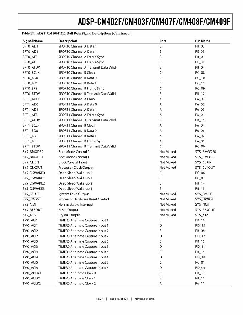
Rev. A | Page 45 of 124 | November 2015
ADSP-CM402F/CM403F/CM407F/CM408F/CM409F
SPT0_AD1 SPORT0 Channel A Data 1 B PB_03SPT0_AD1 SPORT0 Channel A Data 1 E PE_03SPT0_AFS SPORT0 Channel A Frame Sync B PB_01SPT0_AFS SPORT0 Channel A Frame Sync E PE_01SPT0_ATDV SPORT0 Channel A Transmit Data Valid B PB_04SPT0_BCLK SPORT0 Channel B Clock C PC_08SPT0_BD0 SPORT0 Channel B Data 0 C PC_10SPT0_BD1 SPORT0 Channel B Data 1 C PC_11SPT0_BFS SPORT0 Channel B Frame Sync C PC_09SPT0_BTDV SPORT0 Channel B Transmit Data Valid B PB_12SPT1_ACLK SPORT1 Channel A Clock A PA_00SPT1_AD0 SPORT1 Channel A Data 0 A PA_02SPT1_AD1 SPORT1 Channel A Data 1 A PA_03SPT1_AFS SPORT1 Channel A Frame Sync A PA_01SPT1_ATDV SPORT1 Channel A Transmit Data Valid B PB_15SPT1_BCLK SPORT1 Channel B Clock A PA_04SPT1_BD0 SPORT1 Channel B Data 0 A PA_06SPT1_BD1 SPORT1 Channel B Data 1 A PA_07SPT1_BFS SPORT1 Channel B Frame Sync A PA_05SPT1_BTDV SPORT1 Channel B Transmit Data Valid C PC_00SYS_BMODE0 Boot Mode Control 0 Not Muxed SYS_BMODE0SYS_BMODE1 Boot Mode Control 1 Not Muxed SYS_BMODE1SYS_CLKIN Clock/Crystal Input Not Muxed SYS_CLKINSYS_CLKOUT Processor Clock Output Not Muxed SYS_CLKOUTSYS_DSWAKE0 Deep Sleep Wake-up 0 C PC_06SYS_DSWAKE1 Deep Sleep Wake-up 1 C PC_07SYS_DSWAKE2 Deep Sleep Wake-up 2 B PB_14SYS_DSWAKE3 Deep Sleep Wake-up 3 B PB_13SYS_FAULT System Fault Output Not Muxed SYS_FAULTSYS_HWRST Processor Hardware Reset Control Not Muxed SYS_HWRSTSYS_NMI Nonmaskable Interrupt Not Muxed SYS_NMISYS_RESOUT Reset Output Not Muxed SYS_RESOUTSYS_XTAL Crystal Output Not Muxed SYS_XTALTM0_ACI1 TIMER0 Alternate Capture Input 1 B PB_10TM0_ACI1 TIMER0 Alternate Capture Input 1 D PD_13TM0_ACI2 TIMER0 Alternate Capture Input 2 B PB_08TM0_ACI2 TIMER0 Alternate Capture Input 2 D PD_12TM0_ACI3 TIMER0 Alternate Capture Input 3 B PB_12TM0_ACI3 TIMER0 Alternate Capture Input 3 D PD_11TM0_ACI4 TIMER0 Alternate Capture Input 4 B PB_15TM0_ACI4 TIMER0 Alternate Capture Input 4 D PD_10TM0_ACI5 TIMER0 Alternate Capture Input 5 C PC_01TM0_ACI5 TIMER0 Alternate Capture Input 5 D PD_09TM0_ACLK0 TIMER0 Alternate Clock 0 B PB_13TM0_ACLK1 TIMER0 Alternate Clock 1 B PB_11TM0_ACLK2 TIMER0 Alternate Clock 2 A PA_11
Table 18. ADSP-CM409F 212-Ball BGA Signal Descriptions (Continued)
Signal Name Description Port Pin Name
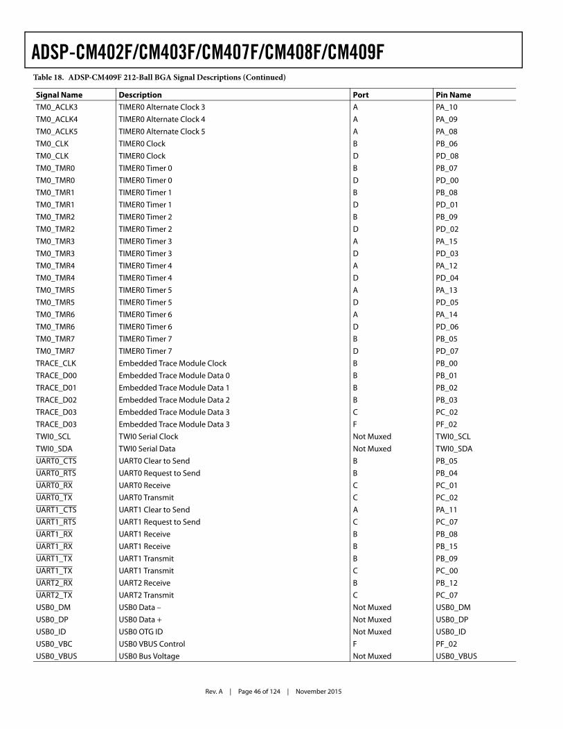
Rev. A | Page 46 of 124 | November 2015
ADSP-CM402F/CM403F/CM407F/CM408F/CM409F
TM0_ACLK3 TIMER0 Alternate Clock 3 A PA_10TM0_ACLK4 TIMER0 Alternate Clock 4 A PA_09TM0_ACLK5 TIMER0 Alternate Clock 5 A PA_08TM0_CLK TIMER0 Clock B PB_06TM0_CLK TIMER0 Clock D PD_08TM0_TMR0 TIMER0 Timer 0 B PB_07TM0_TMR0 TIMER0 Timer 0 D PD_00TM0_TMR1 TIMER0 Timer 1 B PB_08TM0_TMR1 TIMER0 Timer 1 D PD_01TM0_TMR2 TIMER0 Timer 2 B PB_09TM0_TMR2 TIMER0 Timer 2 D PD_02TM0_TMR3 TIMER0 Timer 3 A PA_15TM0_TMR3 TIMER0 Timer 3 D PD_03TM0_TMR4 TIMER0 Timer 4 A PA_12TM0_TMR4 TIMER0 Timer 4 D PD_04TM0_TMR5 TIMER0 Timer 5 A PA_13TM0_TMR5 TIMER0 Timer 5 D PD_05TM0_TMR6 TIMER0 Timer 6 A PA_14TM0_TMR6 TIMER0 Timer 6 D PD_06TM0_TMR7 TIMER0 Timer 7 B PB_05TM0_TMR7 TIMER0 Timer 7 D PD_07TRACE_CLK Embedded Trace Module Clock B PB_00TRACE_D00 Embedded Trace Module Data 0 B PB_01TRACE_D01 Embedded Trace Module Data 1 B PB_02TRACE_D02 Embedded Trace Module Data 2 B PB_03TRACE_D03 Embedded Trace Module Data 3 C PC_02TRACE_D03 Embedded Trace Module Data 3 F PF_02TWI0_SCL TWI0 Serial Clock Not Muxed TWI0_SCLTWI0_SDA TWI0 Serial Data Not Muxed TWI0_SDAUART0_CTS UART0 Clear to Send B PB_05UART0_RTS UART0 Request to Send B PB_04UART0_RX UART0 Receive C PC_01UART0_TX UART0 Transmit C PC_02UART1_CTS UART1 Clear to Send A PA_11UART1_RTS UART1 Request to Send C PC_07UART1_RX UART1 Receive B PB_08UART1_RX UART1 Receive B PB_15UART1_TX UART1 Transmit B PB_09UART1_TX UART1 Transmit C PC_00UART2_RX UART2 Receive B PB_12UART2_TX UART2 Transmit C PC_07USB0_DM USB0 Data – Not Muxed USB0_DMUSB0_DP USB0 Data + Not Muxed USB0_DPUSB0_ID USB0 OTG ID Not Muxed USB0_IDUSB0_VBC USB0 VBUS Control F PF_02USB0_VBUS USB0 Bus Voltage Not Muxed USB0_VBUS
Table 18. ADSP-CM409F 212-Ball BGA Signal Descriptions (Continued)
Signal Name Description Port Pin Name
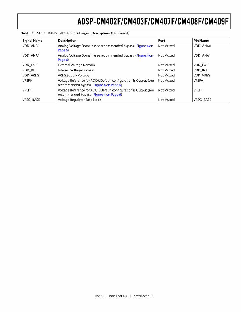
Rev. A | Page 47 of 124 | November 2015
ADSP-CM402F/CM403F/CM407F/CM408F/CM409F
VDD_ANA0 Analog Voltage Domain (see recommended bypass - Figure 4 on Page 6)
Not Muxed VDD_ANA0
VDD_ANA1 Analog Voltage Domain (see recommended bypass - Figure 4 on Page 6)
Not Muxed VDD_ANA1
VDD_EXT External Voltage Domain Not Muxed VDD_EXTVDD_INT Internal Voltage Domain Not Muxed VDD_INTVDD_VREG VREG Supply Voltage Not Muxed VDD_VREGVREF0 Voltage Reference for ADC0. Default configuration is Output (see
recommended bypass - Figure 4 on Page 6)Not Muxed VREF0
VREF1 Voltage Reference for ADC1. Default configuration is Output (see recommended bypass - Figure 4 on Page 6)
Not Muxed VREF1
VREG_BASE Voltage Regulator Base Node Not Muxed VREG_BASE
Table 18. ADSP-CM409F 212-Ball BGA Signal Descriptions (Continued)
Signal Name Description Port Pin Name
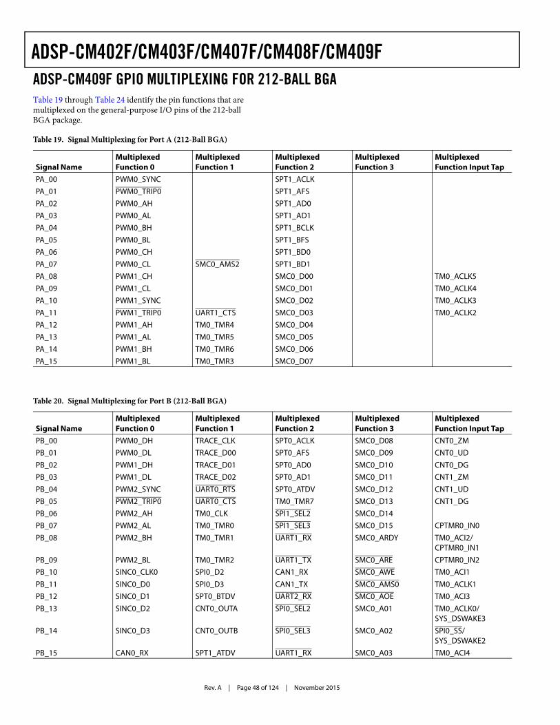
Rev. A | Page 48 of 124 | November 2015
ADSP-CM402F/CM403F/CM407F/CM408F/CM409FADSP-CM409F GPIO MULTIPLEXING FOR 212-BALL BGATable 19 through Table 24 identify the pin functions that are multiplexed on the general-purpose I/O pins of the 212-ball BGA package.
Table 19. Signal Multiplexing for Port A (212-Ball BGA)
Signal NameMultiplexed Function 0
Multiplexed Function 1
Multiplexed Function 2
Multiplexed Function 3
Multiplexed Function Input Tap
PA_00 PWM0_SYNC SPT1_ACLKPA_01 PWM0_TRIP0 SPT1_AFSPA_02 PWM0_AH SPT1_AD0PA_03 PWM0_AL SPT1_AD1PA_04 PWM0_BH SPT1_BCLKPA_05 PWM0_BL SPT1_BFSPA_06 PWM0_CH SPT1_BD0PA_07 PWM0_CL SMC0_AMS2 SPT1_BD1PA_08 PWM1_CH SMC0_D00 TM0_ACLK5PA_09 PWM1_CL SMC0_D01 TM0_ACLK4PA_10 PWM1_SYNC SMC0_D02 TM0_ACLK3PA_11 PWM1_TRIP0 UART1_CTS SMC0_D03 TM0_ACLK2PA_12 PWM1_AH TM0_TMR4 SMC0_D04PA_13 PWM1_AL TM0_TMR5 SMC0_D05PA_14 PWM1_BH TM0_TMR6 SMC0_D06PA_15 PWM1_BL TM0_TMR3 SMC0_D07
Table 20. Signal Multiplexing for Port B (212-Ball BGA)
Signal NameMultiplexed Function 0
Multiplexed Function 1
Multiplexed Function 2
Multiplexed Function 3
Multiplexed Function Input Tap
PB_00 PWM0_DH TRACE_CLK SPT0_ACLK SMC0_D08 CNT0_ZMPB_01 PWM0_DL TRACE_D00 SPT0_AFS SMC0_D09 CNT0_UDPB_02 PWM1_DH TRACE_D01 SPT0_AD0 SMC0_D10 CNT0_DGPB_03 PWM1_DL TRACE_D02 SPT0_AD1 SMC0_D11 CNT1_ZMPB_04 PWM2_SYNC UART0_RTS SPT0_ATDV SMC0_D12 CNT1_UDPB_05 PWM2_TRIP0 UART0_CTS TM0_TMR7 SMC0_D13 CNT1_DGPB_06 PWM2_AH TM0_CLK SPI1_SEL2 SMC0_D14PB_07 PWM2_AL TM0_TMR0 SPI1_SEL3 SMC0_D15 CPTMR0_IN0PB_08 PWM2_BH TM0_TMR1 UART1_RX SMC0_ARDY TM0_ACI2/
CPTMR0_IN1PB_09 PWM2_BL TM0_TMR2 UART1_TX SMC0_ARE CPTMR0_IN2PB_10 SINC0_CLK0 SPI0_D2 CAN1_RX SMC0_AWE TM0_ACI1PB_11 SINC0_D0 SPI0_D3 CAN1_TX SMC0_AMS0 TM0_ACLK1PB_12 SINC0_D1 SPT0_BTDV UART2_RX SMC0_AOE TM0_ACI3PB_13 SINC0_D2 CNT0_OUTA SPI0_SEL2 SMC0_A01 TM0_ACLK0/
SYS_DSWAKE3PB_14 SINC0_D3 CNT0_OUTB SPI0_SEL3 SMC0_A02 SPI0_SS/
SYS_DSWAKE2PB_15 CAN0_RX SPT1_ATDV UART1_RX SMC0_A03 TM0_ACI4
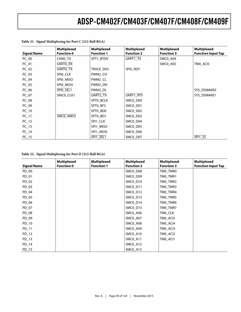
Rev. A | Page 49 of 124 | November 2015
ADSP-CM402F/CM403F/CM407F/CM408F/CM409F
Table 21. Signal Multiplexing for Port C (212-Ball BGA)
Signal NameMultiplexed Function 0
Multiplexed Function 1
Multiplexed Function 2
Multiplexed Function 3
Multiplexed Function Input Tap
PC_00 CAN0_TX SPT1_BTDV UART1_TX SMC0_A04PC_01 UART0_RX SMC0_A05 TM0_ACI5PC_02 UART0_TX TRACE_D03 SPI0_RDYPC_03 SPI0_CLK PWM2_CHPC_04 SPI0_MISO PWM2_CLPC_05 SPI0_MOSI PWM2_DHPC_06 SPI0_SEL1 PWM2_DL SYS_DSWAKE0PC_07 SINC0_CLK1 UART2_TX UART1_RTS SYS_DSWAKE1PC_08 SPT0_BCLK SMC0_D00PC_09 SPT0_BFS SMC0_D01PC_10 SPT0_BD0 SMC0_D02PC_11 SMC0_AMS3 SPT0_BD1 SMC0_D03PC_12 SPI1_CLK SMC0_D04PC_13 SPI1_MISO SMC0_D05PC_14 SPI1_MOSI SMC0_D06PC_15 SPI1_SEL1 SMC0_D07 SPI1_SS
Table 22. Signal Multiplexing for Port D (212-Ball BGA)
Signal NameMultiplexed Function 0
Multiplexed Function 1
Multiplexed Function 2
Multiplexed Function 3
Multiplexed Function Input Tap
PD_00 SMC0_D08 TM0_TMR0PD_01 SMC0_D09 TM0_TMR1PD_02 SMC0_D10 TM0_TMR2PD_03 SMC0_D11 TM0_TMR3PD_04 SMC0_D12 TM0_TMR4PD_05 SMC0_D13 TM0_TMR5PD_06 SMC0_D14 TM0_TMR6PD_07 SMC0_D15 TM0_TMR7PD_08 SMC0_A06 TM0_CLKPD_09 SMC0_A07 TM0_ACI5PD_10 SMC0_A08 TM0_ACI4PD_11 SMC0_A09 TM0_ACI3PD_12 SMC0_A10 TM0_ACI2PD_13 SMC0_A11 TM0_ACI1PD_14 SMC0_A12PD_15 SMC0_A13
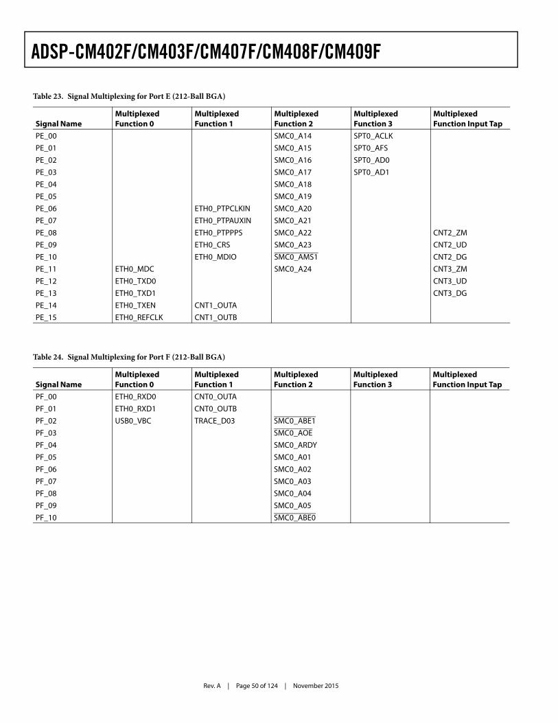
Rev. A | Page 50 of 124 | November 2015
ADSP-CM402F/CM403F/CM407F/CM408F/CM409F
Table 23. Signal Multiplexing for Port E (212-Ball BGA)
Signal NameMultiplexed Function 0
Multiplexed Function 1
Multiplexed Function 2
Multiplexed Function 3
Multiplexed Function Input Tap
PE_00 SMC0_A14 SPT0_ACLKPE_01 SMC0_A15 SPT0_AFSPE_02 SMC0_A16 SPT0_AD0PE_03 SMC0_A17 SPT0_AD1PE_04 SMC0_A18PE_05 SMC0_A19PE_06 ETH0_PTPCLKIN SMC0_A20PE_07 ETH0_PTPAUXIN SMC0_A21PE_08 ETH0_PTPPPS SMC0_A22 CNT2_ZMPE_09 ETH0_CRS SMC0_A23 CNT2_UDPE_10 ETH0_MDIO SMC0_AMS1 CNT2_DGPE_11 ETH0_MDC SMC0_A24 CNT3_ZMPE_12 ETH0_TXD0 CNT3_UDPE_13 ETH0_TXD1 CNT3_DGPE_14 ETH0_TXEN CNT1_OUTAPE_15 ETH0_REFCLK CNT1_OUTB
Table 24. Signal Multiplexing for Port F (212-Ball BGA)
Signal NameMultiplexed Function 0
Multiplexed Function 1
Multiplexed Function 2
Multiplexed Function 3
Multiplexed Function Input Tap
PF_00 ETH0_RXD0 CNT0_OUTAPF_01 ETH0_RXD1 CNT0_OUTBPF_02 USB0_VBC TRACE_D03 SMC0_ABE1PF_03 SMC0_AOEPF_04 SMC0_ARDYPF_05 SMC0_A01PF_06 SMC0_A02PF_07 SMC0_A03PF_08 SMC0_A04PF_09 SMC0_A05PF_10 SMC0_ABE0
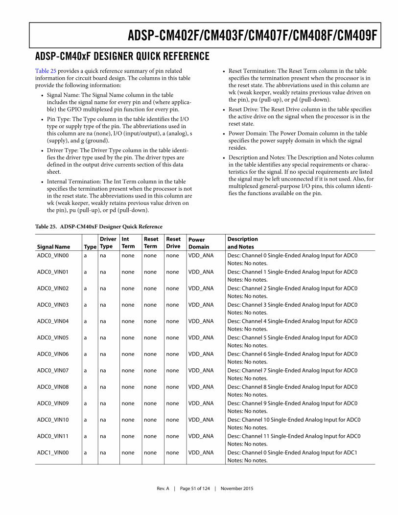
Rev. A | Page 51 of 124 | November 2015
ADSP-CM402F/CM403F/CM407F/CM408F/CM409FADSP-CM40xF DESIGNER QUICK REFERENCETable 25 provides a quick reference summary of pin related information for circuit board design. The columns in this table provide the following information:
• Signal Name: The Signal Name column in the table includes the signal name for every pin and (where applica-ble) the GPIO multiplexed pin function for every pin.
• Pin Type: The Type column in the table identifies the I/O type or supply type of the pin. The abbreviations used in this column are na (none), I/O (input/output), a (analog), s (supply), and g (ground).
• Driver Type: The Driver Type column in the table identi-fies the driver type used by the pin. The driver types are defined in the output drive currents section of this data sheet.
• Internal Termination: The Int Term column in the table specifies the termination present when the processor is not in the reset state. The abbreviations used in this column are wk (weak keeper, weakly retains previous value driven on the pin), pu (pull-up), or pd (pull-down).
• Reset Termination: The Reset Term column in the table specifies the termination present when the processor is in the reset state. The abbreviations used in this column are wk (weak keeper, weakly retains previous value driven on the pin), pu (pull-up), or pd (pull-down).
• Reset Drive: The Reset Drive column in the table specifies the active drive on the signal when the processor is in the reset state.
• Power Domain: The Power Domain column in the table specifies the power supply domain in which the signal resides.
• Description and Notes: The Description and Notes column in the table identifies any special requirements or charac-teristics for the signal. If no special requirements are listed the signal may be left unconnected if it is not used. Also, for multiplexed general-purpose I/O pins, this column identi-fies the functions available on the pin.
Table 25. ADSP-CM40xF Designer Quick Reference
Signal Name TypeDriver Type
Int Term
Reset Term
Reset Drive
Power Domain
Descriptionand Notes
ADC0_VIN00 a na none none none VDD_ANA Desc: Channel 0 Single-Ended Analog Input for ADC0Notes: No notes.
ADC0_VIN01 a na none none none VDD_ANA Desc: Channel 1 Single-Ended Analog Input for ADC0Notes: No notes.
ADC0_VIN02 a na none none none VDD_ANA Desc: Channel 2 Single-Ended Analog Input for ADC0Notes: No notes.
ADC0_VIN03 a na none none none VDD_ANA Desc: Channel 3 Single-Ended Analog Input for ADC0Notes: No notes.
ADC0_VIN04 a na none none none VDD_ANA Desc: Channel 4 Single-Ended Analog Input for ADC0Notes: No notes.
ADC0_VIN05 a na none none none VDD_ANA Desc: Channel 5 Single-Ended Analog Input for ADC0Notes: No notes.
ADC0_VIN06 a na none none none VDD_ANA Desc: Channel 6 Single-Ended Analog Input for ADC0Notes: No notes.
ADC0_VIN07 a na none none none VDD_ANA Desc: Channel 7 Single-Ended Analog Input for ADC0Notes: No notes.
ADC0_VIN08 a na none none none VDD_ANA Desc: Channel 8 Single-Ended Analog Input for ADC0Notes: No notes.
ADC0_VIN09 a na none none none VDD_ANA Desc: Channel 9 Single-Ended Analog Input for ADC0Notes: No notes.
ADC0_VIN10 a na none none none VDD_ANA Desc: Channel 10 Single-Ended Analog Input for ADC0Notes: No notes.
ADC0_VIN11 a na none none none VDD_ANA Desc: Channel 11 Single-Ended Analog Input for ADC0Notes: No notes.
ADC1_VIN00 a na none none none VDD_ANA Desc: Channel 0 Single-Ended Analog Input for ADC1Notes: No notes.
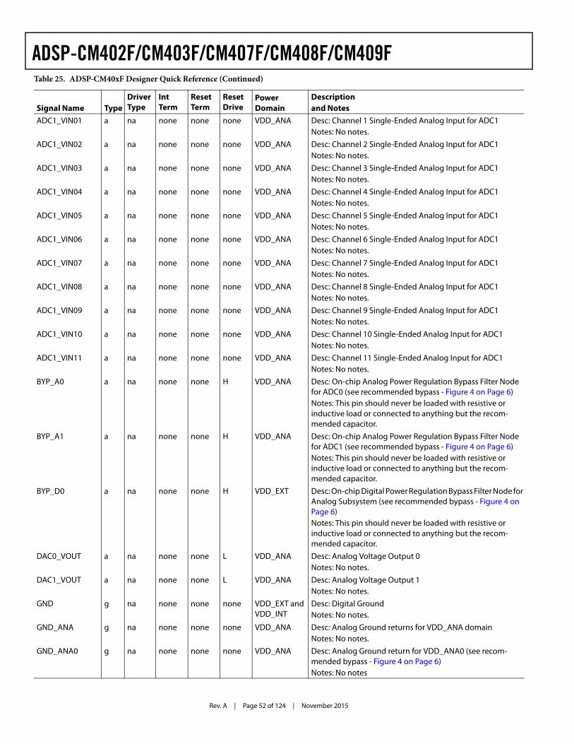
Rev. A | Page 52 of 124 | November 2015
ADSP-CM402F/CM403F/CM407F/CM408F/CM409F
ADC1_VIN01 a na none none none VDD_ANA Desc: Channel 1 Single-Ended Analog Input for ADC1Notes: No notes.
ADC1_VIN02 a na none none none VDD_ANA Desc: Channel 2 Single-Ended Analog Input for ADC1Notes: No notes.
ADC1_VIN03 a na none none none VDD_ANA Desc: Channel 3 Single-Ended Analog Input for ADC1Notes: No notes.
ADC1_VIN04 a na none none none VDD_ANA Desc: Channel 4 Single-Ended Analog Input for ADC1Notes: No notes.
ADC1_VIN05 a na none none none VDD_ANA Desc: Channel 5 Single-Ended Analog Input for ADC1Notes: No notes.
ADC1_VIN06 a na none none none VDD_ANA Desc: Channel 6 Single-Ended Analog Input for ADC1Notes: No notes.
ADC1_VIN07 a na none none none VDD_ANA Desc: Channel 7 Single-Ended Analog Input for ADC1Notes: No notes.
ADC1_VIN08 a na none none none VDD_ANA Desc: Channel 8 Single-Ended Analog Input for ADC1Notes: No notes.
ADC1_VIN09 a na none none none VDD_ANA Desc: Channel 9 Single-Ended Analog Input for ADC1Notes: No notes.
ADC1_VIN10 a na none none none VDD_ANA Desc: Channel 10 Single-Ended Analog Input for ADC1Notes: No notes.
ADC1_VIN11 a na none none none VDD_ANA Desc: Channel 11 Single-Ended Analog Input for ADC1Notes: No notes.
BYP_A0 a na none none H VDD_ANA Desc: On-chip Analog Power Regulation Bypass Filter Node for ADC0 (see recommended bypass - Figure 4 on Page 6)Notes: This pin should never be loaded with resistive or inductive load or connected to anything but the recom-mended capacitor.
BYP_A1 a na none none H VDD_ANA Desc: On-chip Analog Power Regulation Bypass Filter Node for ADC1 (see recommended bypass - Figure 4 on Page 6)Notes: This pin should never be loaded with resistive or inductive load or connected to anything but the recom-mended capacitor.
BYP_D0 a na none none H VDD_EXT Desc: On-chip Digital Power Regulation Bypass Filter Node for Analog Subsystem (see recommended bypass - Figure 4 on Page 6)Notes: This pin should never be loaded with resistive or inductive load or connected to anything but the recom-mended capacitor.
DAC0_VOUT a na none none L VDD_ANA Desc: Analog Voltage Output 0Notes: No notes.
DAC1_VOUT a na none none L VDD_ANA Desc: Analog Voltage Output 1Notes: No notes.
GND g na none none none VDD_EXT and VDD_INT
Desc: Digital GroundNotes: No notes.
GND_ANA g na none none none VDD_ANA Desc: Analog Ground returns for VDD_ANA domainNotes: No notes.
GND_ANA0 g na none none none VDD_ANA Desc: Analog Ground return for VDD_ANA0 (see recom-mended bypass - Figure 4 on Page 6)Notes: No notes
Table 25. ADSP-CM40xF Designer Quick Reference (Continued)
Signal Name TypeDriver Type
Int Term
Reset Term
Reset Drive
Power Domain
Descriptionand Notes
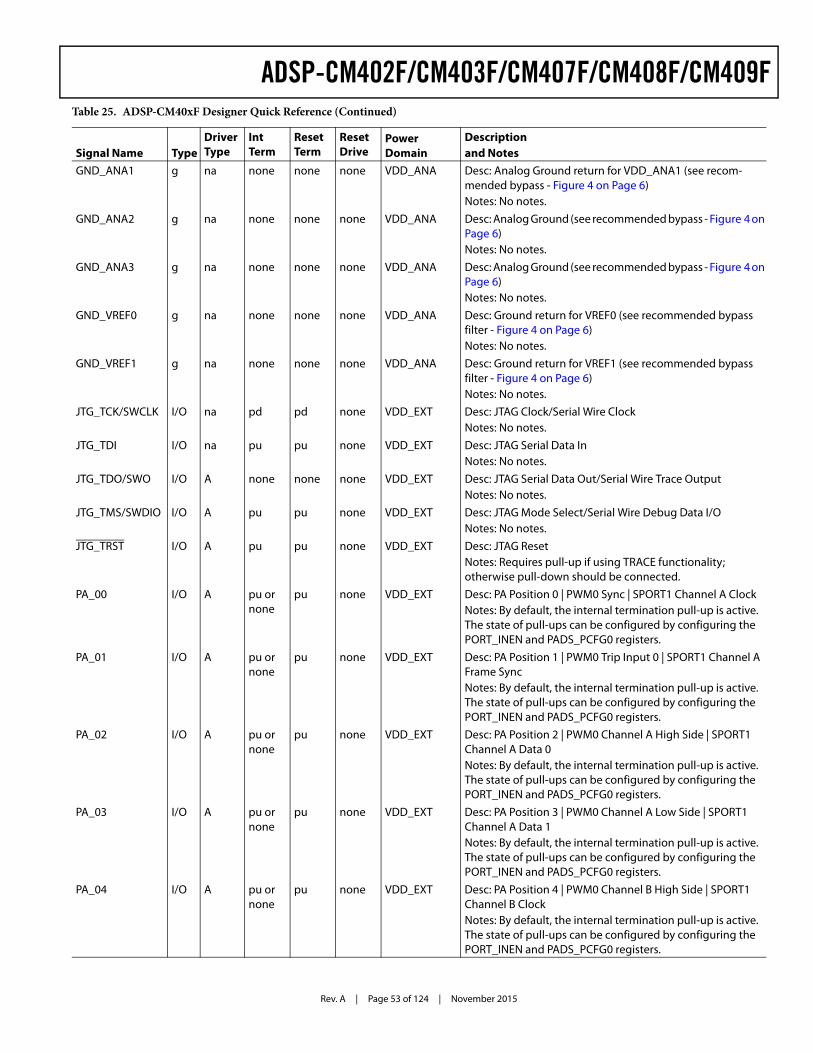
Rev. A | Page 53 of 124 | November 2015
ADSP-CM402F/CM403F/CM407F/CM408F/CM409F
GND_ANA1 g na none none none VDD_ANA Desc: Analog Ground return for VDD_ANA1 (see recom-mended bypass - Figure 4 on Page 6)Notes: No notes.
GND_ANA2 g na none none none VDD_ANA Desc: Analog Ground (see recommended bypass - Figure 4 on Page 6)Notes: No notes.
GND_ANA3 g na none none none VDD_ANA Desc: Analog Ground (see recommended bypass - Figure 4 on Page 6)Notes: No notes.
GND_VREF0 g na none none none VDD_ANA Desc: Ground return for VREF0 (see recommended bypass filter - Figure 4 on Page 6)Notes: No notes.
GND_VREF1 g na none none none VDD_ANA Desc: Ground return for VREF1 (see recommended bypass filter - Figure 4 on Page 6)Notes: No notes.
JTG_TCK/SWCLK I/O na pd pd none VDD_EXT Desc: JTAG Clock/Serial Wire ClockNotes: No notes.
JTG_TDI I/O na pu pu none VDD_EXT Desc: JTAG Serial Data InNotes: No notes.
JTG_TDO/SWO I/O A none none none VDD_EXT Desc: JTAG Serial Data Out/Serial Wire Trace OutputNotes: No notes.
JTG_TMS/SWDIO I/O A pu pu none VDD_EXT Desc: JTAG Mode Select/Serial Wire Debug Data I/ONotes: No notes.
JTG_TRST I/O A pu pu none VDD_EXT Desc: JTAG ResetNotes: Requires pull-up if using TRACE functionality; otherwise pull-down should be connected.
PA_00 I/O A pu or none
pu none VDD_EXT Desc: PA Position 0 | PWM0 Sync | SPORT1 Channel A ClockNotes: By default, the internal termination pull-up is active. The state of pull-ups can be configured by configuring the PORT_INEN and PADS_PCFG0 registers.
PA_01 I/O A pu or none
pu none VDD_EXT Desc: PA Position 1 | PWM0 Trip Input 0 | SPORT1 Channel A Frame SyncNotes: By default, the internal termination pull-up is active. The state of pull-ups can be configured by configuring the PORT_INEN and PADS_PCFG0 registers.
PA_02 I/O A pu or none
pu none VDD_EXT Desc: PA Position 2 | PWM0 Channel A High Side | SPORT1 Channel A Data 0Notes: By default, the internal termination pull-up is active. The state of pull-ups can be configured by configuring the PORT_INEN and PADS_PCFG0 registers.
PA_03 I/O A pu or none
pu none VDD_EXT Desc: PA Position 3 | PWM0 Channel A Low Side | SPORT1 Channel A Data 1Notes: By default, the internal termination pull-up is active. The state of pull-ups can be configured by configuring the PORT_INEN and PADS_PCFG0 registers.
PA_04 I/O A pu or none
pu none VDD_EXT Desc: PA Position 4 | PWM0 Channel B High Side | SPORT1 Channel B ClockNotes: By default, the internal termination pull-up is active. The state of pull-ups can be configured by configuring the PORT_INEN and PADS_PCFG0 registers.
Table 25. ADSP-CM40xF Designer Quick Reference (Continued)
Signal Name TypeDriver Type
Int Term
Reset Term
Reset Drive
Power Domain
Descriptionand Notes
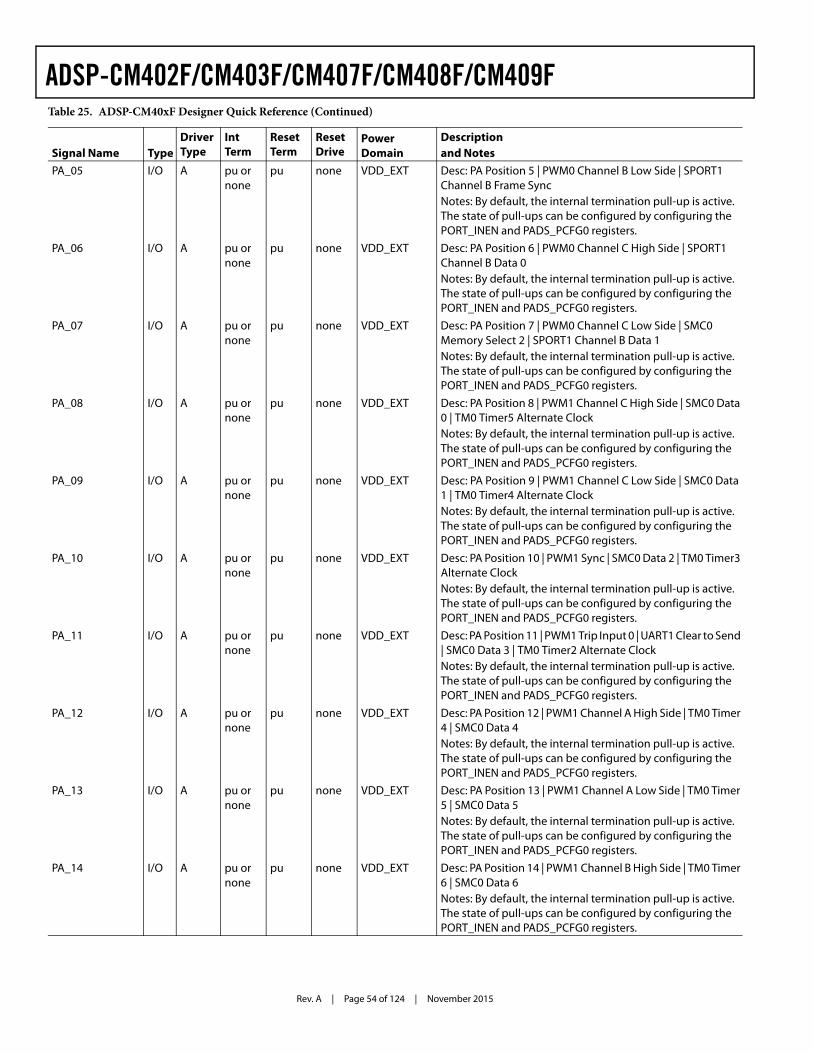
Rev. A | Page 54 of 124 | November 2015
ADSP-CM402F/CM403F/CM407F/CM408F/CM409F
PA_05 I/O A pu or none
pu none VDD_EXT Desc: PA Position 5 | PWM0 Channel B Low Side | SPORT1 Channel B Frame SyncNotes: By default, the internal termination pull-up is active. The state of pull-ups can be configured by configuring the PORT_INEN and PADS_PCFG0 registers.
PA_06 I/O A pu or none
pu none VDD_EXT Desc: PA Position 6 | PWM0 Channel C High Side | SPORT1 Channel B Data 0Notes: By default, the internal termination pull-up is active. The state of pull-ups can be configured by configuring the PORT_INEN and PADS_PCFG0 registers.
PA_07 I/O A pu or none
pu none VDD_EXT Desc: PA Position 7 | PWM0 Channel C Low Side | SMC0 Memory Select 2 | SPORT1 Channel B Data 1Notes: By default, the internal termination pull-up is active. The state of pull-ups can be configured by configuring the PORT_INEN and PADS_PCFG0 registers.
PA_08 I/O A pu or none
pu none VDD_EXT Desc: PA Position 8 | PWM1 Channel C High Side | SMC0 Data 0 | TM0 Timer5 Alternate ClockNotes: By default, the internal termination pull-up is active. The state of pull-ups can be configured by configuring the PORT_INEN and PADS_PCFG0 registers.
PA_09 I/O A pu or none
pu none VDD_EXT Desc: PA Position 9 | PWM1 Channel C Low Side | SMC0 Data 1 | TM0 Timer4 Alternate ClockNotes: By default, the internal termination pull-up is active. The state of pull-ups can be configured by configuring the PORT_INEN and PADS_PCFG0 registers.
PA_10 I/O A pu or none
pu none VDD_EXT Desc: PA Position 10 | PWM1 Sync | SMC0 Data 2 | TM0 Timer3 Alternate ClockNotes: By default, the internal termination pull-up is active. The state of pull-ups can be configured by configuring the PORT_INEN and PADS_PCFG0 registers.
PA_11 I/O A pu or none
pu none VDD_EXT Desc: PA Position 11 | PWM1 Trip Input 0 | UART1 Clear to Send | SMC0 Data 3 | TM0 Timer2 Alternate ClockNotes: By default, the internal termination pull-up is active. The state of pull-ups can be configured by configuring the PORT_INEN and PADS_PCFG0 registers.
PA_12 I/O A pu or none
pu none VDD_EXT Desc: PA Position 12 | PWM1 Channel A High Side | TM0 Timer 4 | SMC0 Data 4Notes: By default, the internal termination pull-up is active. The state of pull-ups can be configured by configuring the PORT_INEN and PADS_PCFG0 registers.
PA_13 I/O A pu or none
pu none VDD_EXT Desc: PA Position 13 | PWM1 Channel A Low Side | TM0 Timer 5 | SMC0 Data 5Notes: By default, the internal termination pull-up is active. The state of pull-ups can be configured by configuring the PORT_INEN and PADS_PCFG0 registers.
PA_14 I/O A pu or none
pu none VDD_EXT Desc: PA Position 14 | PWM1 Channel B High Side | TM0 Timer 6 | SMC0 Data 6Notes: By default, the internal termination pull-up is active. The state of pull-ups can be configured by configuring the PORT_INEN and PADS_PCFG0 registers.
Table 25. ADSP-CM40xF Designer Quick Reference (Continued)
Signal Name TypeDriver Type
Int Term
Reset Term
Reset Drive
Power Domain
Descriptionand Notes
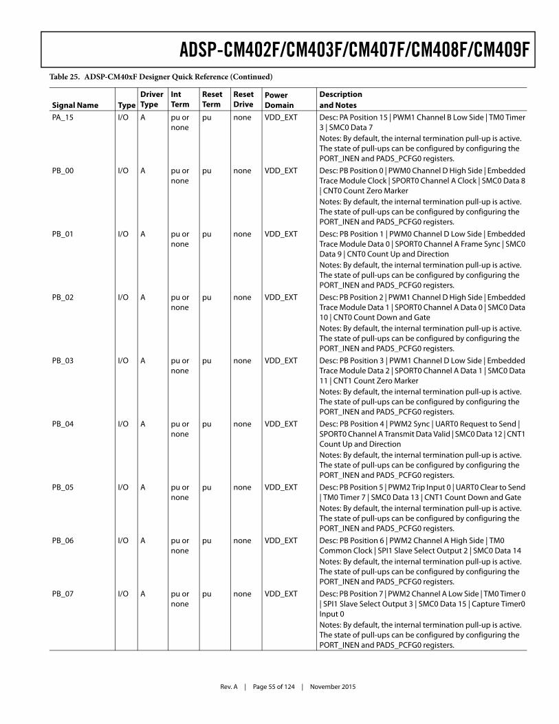
Rev. A | Page 55 of 124 | November 2015
ADSP-CM402F/CM403F/CM407F/CM408F/CM409F
PA_15 I/O A pu or none
pu none VDD_EXT Desc: PA Position 15 | PWM1 Channel B Low Side | TM0 Timer 3 | SMC0 Data 7Notes: By default, the internal termination pull-up is active. The state of pull-ups can be configured by configuring the PORT_INEN and PADS_PCFG0 registers.
PB_00 I/O A pu or none
pu none VDD_EXT Desc: PB Position 0 | PWM0 Channel D High Side | Embedded Trace Module Clock | SPORT0 Channel A Clock | SMC0 Data 8 | CNT0 Count Zero MarkerNotes: By default, the internal termination pull-up is active. The state of pull-ups can be configured by configuring the PORT_INEN and PADS_PCFG0 registers.
PB_01 I/O A pu or none
pu none VDD_EXT Desc: PB Position 1 | PWM0 Channel D Low Side | Embedded Trace Module Data 0 | SPORT0 Channel A Frame Sync | SMC0 Data 9 | CNT0 Count Up and DirectionNotes: By default, the internal termination pull-up is active. The state of pull-ups can be configured by configuring the PORT_INEN and PADS_PCFG0 registers.
PB_02 I/O A pu or none
pu none VDD_EXT Desc: PB Position 2 | PWM1 Channel D High Side | Embedded Trace Module Data 1 | SPORT0 Channel A Data 0 | SMC0 Data 10 | CNT0 Count Down and GateNotes: By default, the internal termination pull-up is active. The state of pull-ups can be configured by configuring the PORT_INEN and PADS_PCFG0 registers.
PB_03 I/O A pu or none
pu none VDD_EXT Desc: PB Position 3 | PWM1 Channel D Low Side | Embedded Trace Module Data 2 | SPORT0 Channel A Data 1 | SMC0 Data 11 | CNT1 Count Zero MarkerNotes: By default, the internal termination pull-up is active. The state of pull-ups can be configured by configuring the PORT_INEN and PADS_PCFG0 registers.
PB_04 I/O A pu or none
pu none VDD_EXT Desc: PB Position 4 | PWM2 Sync | UART0 Request to Send | SPORT0 Channel A Transmit Data Valid | SMC0 Data 12 | CNT1 Count Up and DirectionNotes: By default, the internal termination pull-up is active. The state of pull-ups can be configured by configuring the PORT_INEN and PADS_PCFG0 registers.
PB_05 I/O A pu or none
pu none VDD_EXT Desc: PB Position 5 | PWM2 Trip Input 0 | UART0 Clear to Send | TM0 Timer 7 | SMC0 Data 13 | CNT1 Count Down and GateNotes: By default, the internal termination pull-up is active. The state of pull-ups can be configured by configuring the PORT_INEN and PADS_PCFG0 registers.
PB_06 I/O A pu or none
pu none VDD_EXT Desc: PB Position 6 | PWM2 Channel A High Side | TM0 Common Clock | SPI1 Slave Select Output 2 | SMC0 Data 14Notes: By default, the internal termination pull-up is active. The state of pull-ups can be configured by configuring the PORT_INEN and PADS_PCFG0 registers.
PB_07 I/O A pu or none
pu none VDD_EXT Desc: PB Position 7 | PWM2 Channel A Low Side | TM0 Timer 0 | SPI1 Slave Select Output 3 | SMC0 Data 15 | Capture Timer0 Input 0Notes: By default, the internal termination pull-up is active. The state of pull-ups can be configured by configuring the PORT_INEN and PADS_PCFG0 registers.
Table 25. ADSP-CM40xF Designer Quick Reference (Continued)
Signal Name TypeDriver Type
Int Term
Reset Term
Reset Drive
Power Domain
Descriptionand Notes
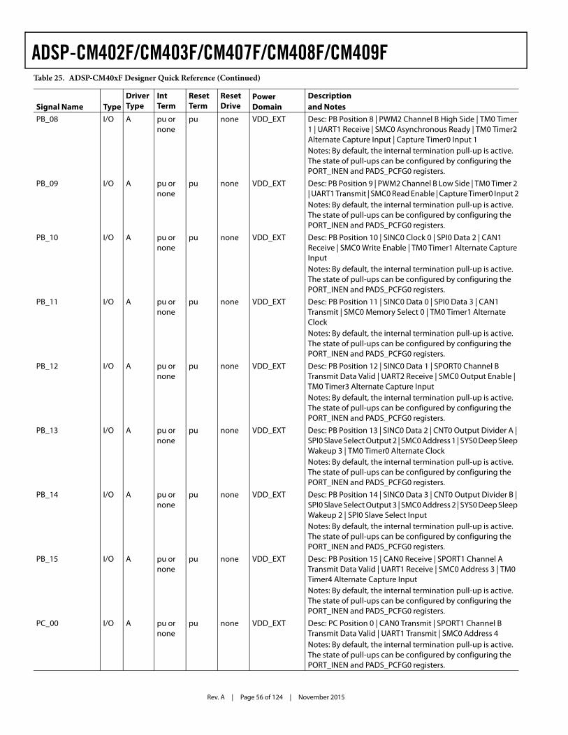
Rev. A | Page 56 of 124 | November 2015
ADSP-CM402F/CM403F/CM407F/CM408F/CM409F
PB_08 I/O A pu or none
pu none VDD_EXT Desc: PB Position 8 | PWM2 Channel B High Side | TM0 Timer 1 | UART1 Receive | SMC0 Asynchronous Ready | TM0 Timer2 Alternate Capture Input | Capture Timer0 Input 1Notes: By default, the internal termination pull-up is active. The state of pull-ups can be configured by configuring the PORT_INEN and PADS_PCFG0 registers.
PB_09 I/O A pu or none
pu none VDD_EXT Desc: PB Position 9 | PWM2 Channel B Low Side | TM0 Timer 2 | UART1 Transmit | SMC0 Read Enable | Capture Timer0 Input 2Notes: By default, the internal termination pull-up is active. The state of pull-ups can be configured by configuring the PORT_INEN and PADS_PCFG0 registers.
PB_10 I/O A pu or none
pu none VDD_EXT Desc: PB Position 10 | SINC0 Clock 0 | SPI0 Data 2 | CAN1 Receive | SMC0 Write Enable | TM0 Timer1 Alternate Capture InputNotes: By default, the internal termination pull-up is active. The state of pull-ups can be configured by configuring the PORT_INEN and PADS_PCFG0 registers.
PB_11 I/O A pu or none
pu none VDD_EXT Desc: PB Position 11 | SINC0 Data 0 | SPI0 Data 3 | CAN1 Transmit | SMC0 Memory Select 0 | TM0 Timer1 Alternate ClockNotes: By default, the internal termination pull-up is active. The state of pull-ups can be configured by configuring the PORT_INEN and PADS_PCFG0 registers.
PB_12 I/O A pu or none
pu none VDD_EXT Desc: PB Position 12 | SINC0 Data 1 | SPORT0 Channel B Transmit Data Valid | UART2 Receive | SMC0 Output Enable | TM0 Timer3 Alternate Capture InputNotes: By default, the internal termination pull-up is active. The state of pull-ups can be configured by configuring the PORT_INEN and PADS_PCFG0 registers.
PB_13 I/O A pu or none
pu none VDD_EXT Desc: PB Position 13 | SINC0 Data 2 | CNT0 Output Divider A | SPI0 Slave Select Output 2 | SMC0 Address 1 | SYS0 Deep Sleep Wakeup 3 | TM0 Timer0 Alternate ClockNotes: By default, the internal termination pull-up is active. The state of pull-ups can be configured by configuring the PORT_INEN and PADS_PCFG0 registers.
PB_14 I/O A pu or none
pu none VDD_EXT Desc: PB Position 14 | SINC0 Data 3 | CNT0 Output Divider B | SPI0 Slave Select Output 3 | SMC0 Address 2 | SYS0 Deep Sleep Wakeup 2 | SPI0 Slave Select InputNotes: By default, the internal termination pull-up is active. The state of pull-ups can be configured by configuring the PORT_INEN and PADS_PCFG0 registers.
PB_15 I/O A pu or none
pu none VDD_EXT Desc: PB Position 15 | CAN0 Receive | SPORT1 Channel A Transmit Data Valid | UART1 Receive | SMC0 Address 3 | TM0 Timer4 Alternate Capture InputNotes: By default, the internal termination pull-up is active. The state of pull-ups can be configured by configuring the PORT_INEN and PADS_PCFG0 registers.
PC_00 I/O A pu or none
pu none VDD_EXT Desc: PC Position 0 | CAN0 Transmit | SPORT1 Channel B Transmit Data Valid | UART1 Transmit | SMC0 Address 4Notes: By default, the internal termination pull-up is active. The state of pull-ups can be configured by configuring the PORT_INEN and PADS_PCFG0 registers.
Table 25. ADSP-CM40xF Designer Quick Reference (Continued)
Signal Name TypeDriver Type
Int Term
Reset Term
Reset Drive
Power Domain
Descriptionand Notes
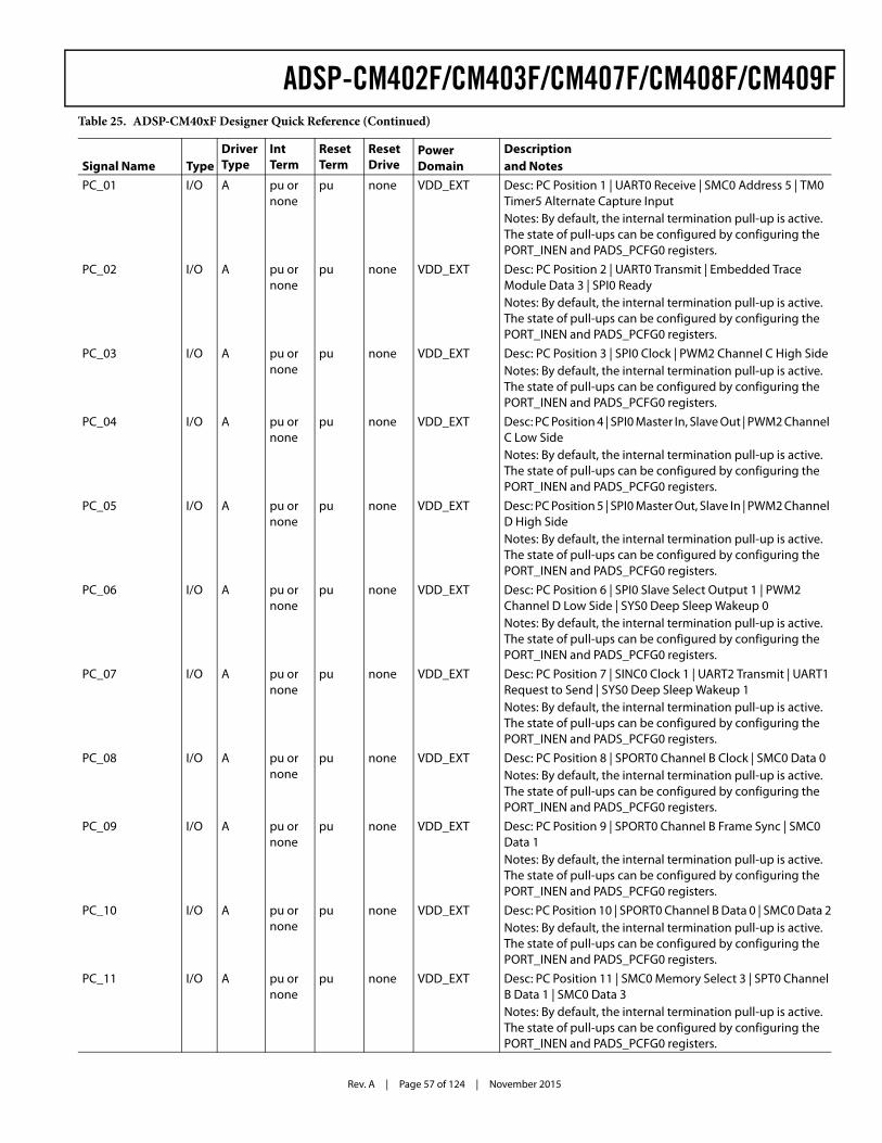
Rev. A | Page 57 of 124 | November 2015
ADSP-CM402F/CM403F/CM407F/CM408F/CM409F
PC_01 I/O A pu or none
pu none VDD_EXT Desc: PC Position 1 | UART0 Receive | SMC0 Address 5 | TM0 Timer5 Alternate Capture InputNotes: By default, the internal termination pull-up is active. The state of pull-ups can be configured by configuring the PORT_INEN and PADS_PCFG0 registers.
PC_02 I/O A pu or none
pu none VDD_EXT Desc: PC Position 2 | UART0 Transmit | Embedded Trace Module Data 3 | SPI0 ReadyNotes: By default, the internal termination pull-up is active. The state of pull-ups can be configured by configuring the PORT_INEN and PADS_PCFG0 registers.
PC_03 I/O A pu or none
pu none VDD_EXT Desc: PC Position 3 | SPI0 Clock | PWM2 Channel C High SideNotes: By default, the internal termination pull-up is active. The state of pull-ups can be configured by configuring the PORT_INEN and PADS_PCFG0 registers.
PC_04 I/O A pu or none
pu none VDD_EXT Desc: PC Position 4 | SPI0 Master In, Slave Out | PWM2 Channel C Low SideNotes: By default, the internal termination pull-up is active. The state of pull-ups can be configured by configuring the PORT_INEN and PADS_PCFG0 registers.
PC_05 I/O A pu or none
pu none VDD_EXT Desc: PC Position 5 | SPI0 Master Out, Slave In | PWM2 Channel D High SideNotes: By default, the internal termination pull-up is active. The state of pull-ups can be configured by configuring the PORT_INEN and PADS_PCFG0 registers.
PC_06 I/O A pu or none
pu none VDD_EXT Desc: PC Position 6 | SPI0 Slave Select Output 1 | PWM2 Channel D Low Side | SYS0 Deep Sleep Wakeup 0Notes: By default, the internal termination pull-up is active. The state of pull-ups can be configured by configuring the PORT_INEN and PADS_PCFG0 registers.
PC_07 I/O A pu or none
pu none VDD_EXT Desc: PC Position 7 | SINC0 Clock 1 | UART2 Transmit | UART1 Request to Send | SYS0 Deep Sleep Wakeup 1Notes: By default, the internal termination pull-up is active. The state of pull-ups can be configured by configuring the PORT_INEN and PADS_PCFG0 registers.
PC_08 I/O A pu or none
pu none VDD_EXT Desc: PC Position 8 | SPORT0 Channel B Clock | SMC0 Data 0Notes: By default, the internal termination pull-up is active. The state of pull-ups can be configured by configuring the PORT_INEN and PADS_PCFG0 registers.
PC_09 I/O A pu or none
pu none VDD_EXT Desc: PC Position 9 | SPORT0 Channel B Frame Sync | SMC0 Data 1Notes: By default, the internal termination pull-up is active. The state of pull-ups can be configured by configuring the PORT_INEN and PADS_PCFG0 registers.
PC_10 I/O A pu or none
pu none VDD_EXT Desc: PC Position 10 | SPORT0 Channel B Data 0 | SMC0 Data 2Notes: By default, the internal termination pull-up is active. The state of pull-ups can be configured by configuring the PORT_INEN and PADS_PCFG0 registers.
PC_11 I/O A pu or none
pu none VDD_EXT Desc: PC Position 11 | SMC0 Memory Select 3 | SPT0 Channel B Data 1 | SMC0 Data 3Notes: By default, the internal termination pull-up is active. The state of pull-ups can be configured by configuring the PORT_INEN and PADS_PCFG0 registers.
Table 25. ADSP-CM40xF Designer Quick Reference (Continued)
Signal Name TypeDriver Type
Int Term
Reset Term
Reset Drive
Power Domain
Descriptionand Notes
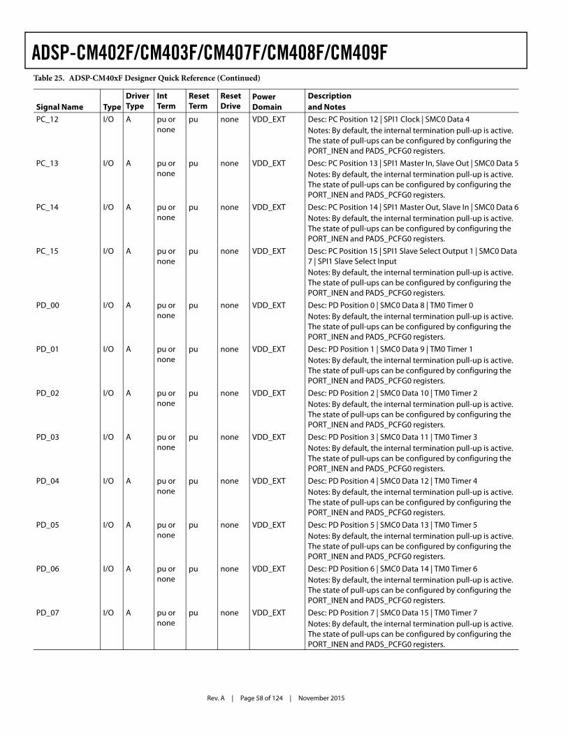
Rev. A | Page 58 of 124 | November 2015
ADSP-CM402F/CM403F/CM407F/CM408F/CM409F
PC_12 I/O A pu or none
pu none VDD_EXT Desc: PC Position 12 | SPI1 Clock | SMC0 Data 4Notes: By default, the internal termination pull-up is active. The state of pull-ups can be configured by configuring the PORT_INEN and PADS_PCFG0 registers.
PC_13 I/O A pu or none
pu none VDD_EXT Desc: PC Position 13 | SPI1 Master In, Slave Out | SMC0 Data 5Notes: By default, the internal termination pull-up is active. The state of pull-ups can be configured by configuring the PORT_INEN and PADS_PCFG0 registers.
PC_14 I/O A pu or none
pu none VDD_EXT Desc: PC Position 14 | SPI1 Master Out, Slave In | SMC0 Data 6Notes: By default, the internal termination pull-up is active. The state of pull-ups can be configured by configuring the PORT_INEN and PADS_PCFG0 registers.
PC_15 I/O A pu or none
pu none VDD_EXT Desc: PC Position 15 | SPI1 Slave Select Output 1 | SMC0 Data 7 | SPI1 Slave Select InputNotes: By default, the internal termination pull-up is active. The state of pull-ups can be configured by configuring the PORT_INEN and PADS_PCFG0 registers.
PD_00 I/O A pu or none
pu none VDD_EXT Desc: PD Position 0 | SMC0 Data 8 | TM0 Timer 0Notes: By default, the internal termination pull-up is active. The state of pull-ups can be configured by configuring the PORT_INEN and PADS_PCFG0 registers.
PD_01 I/O A pu or none
pu none VDD_EXT Desc: PD Position 1 | SMC0 Data 9 | TM0 Timer 1Notes: By default, the internal termination pull-up is active. The state of pull-ups can be configured by configuring the PORT_INEN and PADS_PCFG0 registers.
PD_02 I/O A pu or none
pu none VDD_EXT Desc: PD Position 2 | SMC0 Data 10 | TM0 Timer 2Notes: By default, the internal termination pull-up is active. The state of pull-ups can be configured by configuring the PORT_INEN and PADS_PCFG0 registers.
PD_03 I/O A pu or none
pu none VDD_EXT Desc: PD Position 3 | SMC0 Data 11 | TM0 Timer 3Notes: By default, the internal termination pull-up is active. The state of pull-ups can be configured by configuring the PORT_INEN and PADS_PCFG0 registers.
PD_04 I/O A pu or none
pu none VDD_EXT Desc: PD Position 4 | SMC0 Data 12 | TM0 Timer 4Notes: By default, the internal termination pull-up is active. The state of pull-ups can be configured by configuring the PORT_INEN and PADS_PCFG0 registers.
PD_05 I/O A pu or none
pu none VDD_EXT Desc: PD Position 5 | SMC0 Data 13 | TM0 Timer 5Notes: By default, the internal termination pull-up is active. The state of pull-ups can be configured by configuring the PORT_INEN and PADS_PCFG0 registers.
PD_06 I/O A pu or none
pu none VDD_EXT Desc: PD Position 6 | SMC0 Data 14 | TM0 Timer 6Notes: By default, the internal termination pull-up is active. The state of pull-ups can be configured by configuring the PORT_INEN and PADS_PCFG0 registers.
PD_07 I/O A pu or none
pu none VDD_EXT Desc: PD Position 7 | SMC0 Data 15 | TM0 Timer 7Notes: By default, the internal termination pull-up is active. The state of pull-ups can be configured by configuring the PORT_INEN and PADS_PCFG0 registers.
Table 25. ADSP-CM40xF Designer Quick Reference (Continued)
Signal Name TypeDriver Type
Int Term
Reset Term
Reset Drive
Power Domain
Descriptionand Notes
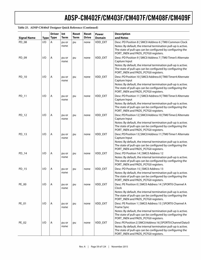
Rev. A | Page 59 of 124 | November 2015
ADSP-CM402F/CM403F/CM407F/CM408F/CM409F
PD_08 I/O A pu or none
pu none VDD_EXT Desc: PD Position 8 | SMC0 Address 6 | TM0 Common ClockNotes: By default, the internal termination pull-up is active. The state of pull-ups can be configured by configuring the PORT_INEN and PADS_PCFG0 registers.
PD_09 I/O A pu or none
pu none VDD_EXT Desc: PD Position 9 | SMC0 Address 7 | TM0 Timer5 Alternate Capture InputNotes: By default, the internal termination pull-up is active. The state of pull-ups can be configured by configuring the PORT_INEN and PADS_PCFG0 registers.
PD_10 I/O A pu or none
pu none VDD_EXT Desc: PD Position 10 | SMC0 Address 8 | TM0 Timer4 Alternate Capture InputNotes: By default, the internal termination pull-up is active. The state of pull-ups can be configured by configuring the PORT_INEN and PADS_PCFG0 registers.
PD_11 I/O A pu or none
pu none VDD_EXT Desc: PD Position 11 | SMC0 Address 9 | TM0 Timer3 Alternate Capture InputNotes: By default, the internal termination pull-up is active. The state of pull-ups can be configured by configuring the PORT_INEN and PADS_PCFG0 registers.
PD_12 I/O A pu or none
pu none VDD_EXT Desc: PD Position 12 | SMC0 Address 10 | TM0 Timer2 Alternate Capture InputNotes: By default, the internal termination pull-up is active. The state of pull-ups can be configured by configuring the PORT_INEN and PADS_PCFG0 registers.
PD_13 I/O A pu or none
pu none VDD_EXT Desc: PD Position 13 | SMC0 Address 11 | TM0 Timer1 Alternate Capture InputNotes: By default, the internal termination pull-up is active. The state of pull-ups can be configured by configuring the PORT_INEN and PADS_PCFG0 registers.
PD_14 I/O A pu or none
pu none VDD_EXT Desc: PD Position 14 | SMC0 Address 12Notes: By default, the internal termination pull-up is active. The state of pull-ups can be configured by configuring the PORT_INEN and PADS_PCFG0 registers.
PD_15 I/O A pu or none
pu none VDD_EXT Desc: PD Position 15 | SMC0 Address 13Notes: By default, the internal termination pull-up is active. The state of pull-ups can be configured by configuring the PORT_INEN and PADS_PCFG0 registers.
PE_00 I/O A pu or none
pu none VDD_EXT Desc: PE Position 0 | SMC0 Address 14 | SPORT0 Channel A ClockNotes: By default, the internal termination pull-up is active. The state of pull-ups can be configured by configuring the PORT_INEN and PADS_PCFG0 registers.
PE_01 I/O A pu or none
pu none VDD_EXT Desc: PE Position 1 | SMC0 Address 15 | SPORT0 Channel A Frame SyncNotes: By default, the internal termination pull-up is active. The state of pull-ups can be configured by configuring the PORT_INEN and PADS_PCFG0 registers.
PE_02 I/O A pu or none
pu none VDD_EXT Desc: PE Position 2 | SMC0 Address 16 | SPORT0 Channel Data 0Notes: By default, the internal termination pull-up is active. The state of pull-ups can be configured by configuring the PORT_INEN and PADS_PCFG0 registers.
Table 25. ADSP-CM40xF Designer Quick Reference (Continued)
Signal Name TypeDriver Type
Int Term
Reset Term
Reset Drive
Power Domain
Descriptionand Notes
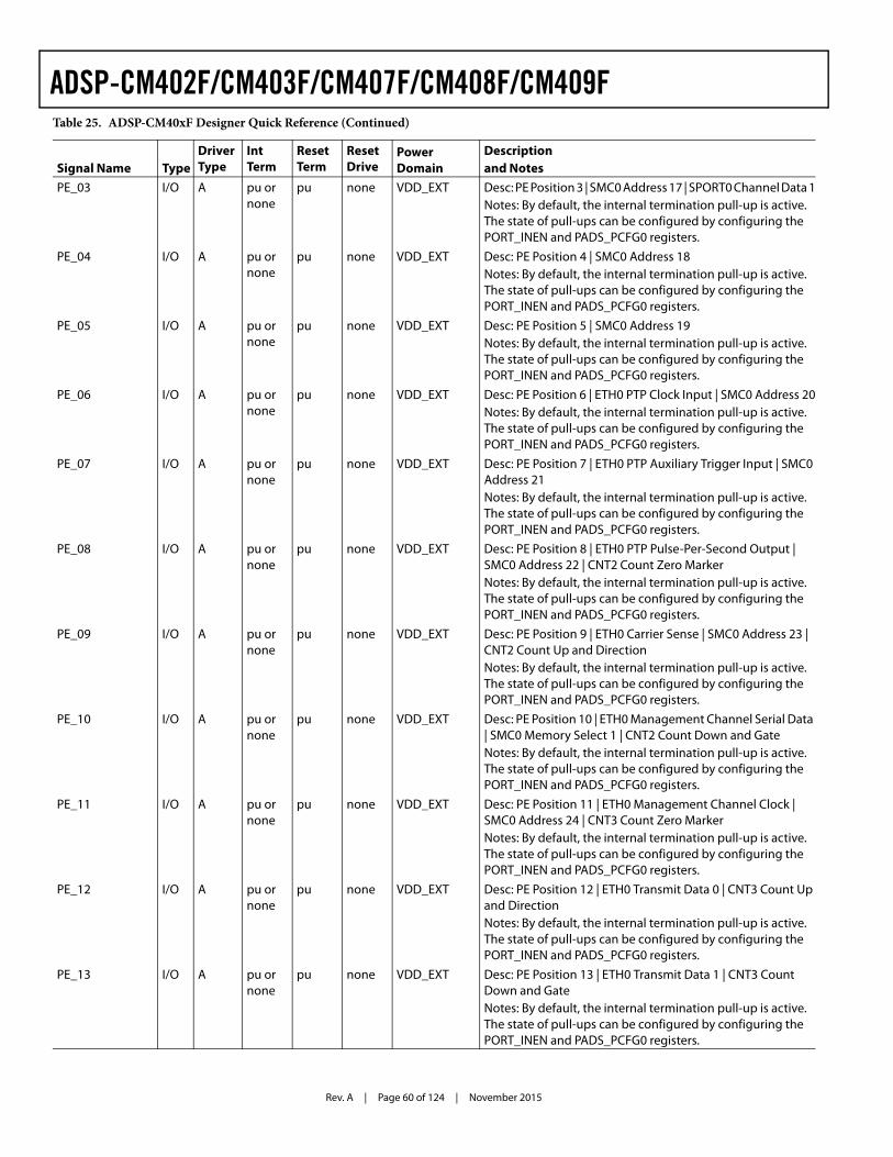
Rev. A | Page 60 of 124 | November 2015
ADSP-CM402F/CM403F/CM407F/CM408F/CM409F
PE_03 I/O A pu or none
pu none VDD_EXT Desc: PE Position 3 | SMC0 Address 17 | SPORT0 Channel Data 1Notes: By default, the internal termination pull-up is active. The state of pull-ups can be configured by configuring the PORT_INEN and PADS_PCFG0 registers.
PE_04 I/O A pu or none
pu none VDD_EXT Desc: PE Position 4 | SMC0 Address 18Notes: By default, the internal termination pull-up is active. The state of pull-ups can be configured by configuring the PORT_INEN and PADS_PCFG0 registers.
PE_05 I/O A pu or none
pu none VDD_EXT Desc: PE Position 5 | SMC0 Address 19Notes: By default, the internal termination pull-up is active. The state of pull-ups can be configured by configuring the PORT_INEN and PADS_PCFG0 registers.
PE_06 I/O A pu or none
pu none VDD_EXT Desc: PE Position 6 | ETH0 PTP Clock Input | SMC0 Address 20Notes: By default, the internal termination pull-up is active. The state of pull-ups can be configured by configuring the PORT_INEN and PADS_PCFG0 registers.
PE_07 I/O A pu or none
pu none VDD_EXT Desc: PE Position 7 | ETH0 PTP Auxiliary Trigger Input | SMC0 Address 21Notes: By default, the internal termination pull-up is active. The state of pull-ups can be configured by configuring the PORT_INEN and PADS_PCFG0 registers.
PE_08 I/O A pu or none
pu none VDD_EXT Desc: PE Position 8 | ETH0 PTP Pulse-Per-Second Output | SMC0 Address 22 | CNT2 Count Zero MarkerNotes: By default, the internal termination pull-up is active. The state of pull-ups can be configured by configuring the PORT_INEN and PADS_PCFG0 registers.
PE_09 I/O A pu or none
pu none VDD_EXT Desc: PE Position 9 | ETH0 Carrier Sense | SMC0 Address 23 | CNT2 Count Up and DirectionNotes: By default, the internal termination pull-up is active. The state of pull-ups can be configured by configuring the PORT_INEN and PADS_PCFG0 registers.
PE_10 I/O A pu or none
pu none VDD_EXT Desc: PE Position 10 | ETH0 Management Channel Serial Data | SMC0 Memory Select 1 | CNT2 Count Down and GateNotes: By default, the internal termination pull-up is active. The state of pull-ups can be configured by configuring the PORT_INEN and PADS_PCFG0 registers.
PE_11 I/O A pu or none
pu none VDD_EXT Desc: PE Position 11 | ETH0 Management Channel Clock | SMC0 Address 24 | CNT3 Count Zero MarkerNotes: By default, the internal termination pull-up is active. The state of pull-ups can be configured by configuring the PORT_INEN and PADS_PCFG0 registers.
PE_12 I/O A pu or none
pu none VDD_EXT Desc: PE Position 12 | ETH0 Transmit Data 0 | CNT3 Count Up and DirectionNotes: By default, the internal termination pull-up is active. The state of pull-ups can be configured by configuring the PORT_INEN and PADS_PCFG0 registers.
PE_13 I/O A pu or none
pu none VDD_EXT Desc: PE Position 13 | ETH0 Transmit Data 1 | CNT3 Count Down and GateNotes: By default, the internal termination pull-up is active. The state of pull-ups can be configured by configuring the PORT_INEN and PADS_PCFG0 registers.
Table 25. ADSP-CM40xF Designer Quick Reference (Continued)
Signal Name TypeDriver Type
Int Term
Reset Term
Reset Drive
Power Domain
Descriptionand Notes
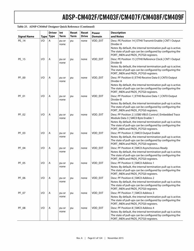
Rev. A | Page 61 of 124 | November 2015
ADSP-CM402F/CM403F/CM407F/CM408F/CM409F
PE_14 I/O A pu or none
pu none VDD_EXT Desc: PE Position 14 | ETH0 Transmit Enable | CNT1 Output Divider ANotes: By default, the internal termination pull-up is active. The state of pull-ups can be configured by configuring the PORT_INEN and PADS_PCFG0 registers.
PE_15 I/O A pu or none
pu none VDD_EXT Desc: PE Position 15 | ETH0 Reference Clock | CNT1 Output Divider BNotes: By default, the internal termination pull-up is active. The state of pull-ups can be configured by configuring the PORT_INEN and PADS_PCFG0 registers.
PF_00 I/O A pu or none
pu none VDD_EXT Desc: PF Position 0 | ETH0 Receive Data 0 | CNT0 Output Divider ANotes: By default, the internal termination pull-up is active. The state of pull-ups can be configured by configuring the PORT_INEN and PADS_PCFG0 registers.
PF_01 I/O A pu or none
pu none VDD_EXT Desc: PF Position 1 | ETH0 Receive Data 1 | CNT0 Output Divider BNotes: By default, the internal termination pull-up is active. The state of pull-ups can be configured by configuring the PORT_INEN and PADS_PCFG0 registers.
PF_02 I/O A pu or none
pu none VDD_EXT Desc: PF Position 2 | USB0 VBUS Control | Embedded Trace Module Data 3 | SMC0 Byte Enable 1Notes: By default, the internal termination pull-up is active. The state of pull-ups can be configured by configuring the PORT_INEN and PADS_PCFG0 registers.
PF_03 I/O A pu or none
pu none VDD_EXT Desc: PF Position 3 | SMC0 Output EnableNotes: By default, the internal termination pull-up is active. The state of pull-ups can be configured by configuring the PORT_INEN and PADS_PCFG0 registers.
PF_04 I/O A pu or none
pu none VDD_EXT Desc: PF Position 4 | SMC0 Asynchronous ReadyNotes: By default, the internal termination pull-up is active. The state of pull-ups can be configured by configuring the PORT_INEN and PADS_PCFG0 registers.
PF_05 I/O A pu or none
pu none VDD_EXT Desc: PF Position 5 | SMC0 Address 1Notes: By default, the internal termination pull-up is active. The state of pull-ups can be configured by configuring the PORT_INEN and PADS_PCFG0 registers.
PF_06 I/O A pu or none
pu none VDD_EXT Desc: PF Position 6 | SMC0 Address 2Notes: By default, the internal termination pull-up is active. The state of pull-ups can be configured by configuring the PORT_INEN and PADS_PCFG0 registers.
PF_07 I/O A pu or none
pu none VDD_EXT Desc: PF Position 7 | SMC0 Address 3Notes: By default, the internal termination pull-up is active. The state of pull-ups can be configured by configuring the PORT_INEN and PADS_PCFG0 registers.
PF_08 I/O A pu or none
pu none VDD_EXT Desc: PF Position 8 | SMC0 Address 4Notes: By default, the internal termination pull-up is active. The state of pull-ups can be configured by configuring the PORT_INEN and PADS_PCFG0 registers.
Table 25. ADSP-CM40xF Designer Quick Reference (Continued)
Signal Name TypeDriver Type
Int Term
Reset Term
Reset Drive
Power Domain
Descriptionand Notes
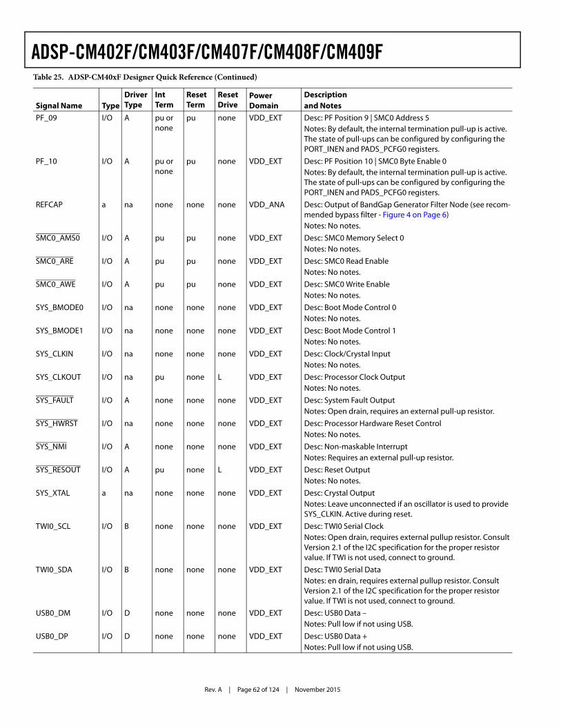
Rev. A | Page 62 of 124 | November 2015
ADSP-CM402F/CM403F/CM407F/CM408F/CM409F
PF_09 I/O A pu or none
pu none VDD_EXT Desc: PF Position 9 | SMC0 Address 5Notes: By default, the internal termination pull-up is active. The state of pull-ups can be configured by configuring the PORT_INEN and PADS_PCFG0 registers.
PF_10 I/O A pu or none
pu none VDD_EXT Desc: PF Position 10 | SMC0 Byte Enable 0Notes: By default, the internal termination pull-up is active. The state of pull-ups can be configured by configuring the PORT_INEN and PADS_PCFG0 registers.
REFCAP a na none none none VDD_ANA Desc: Output of BandGap Generator Filter Node (see recom-mended bypass filter - Figure 4 on Page 6)Notes: No notes.
SMC0_AMS0 I/O A pu pu none VDD_EXT Desc: SMC0 Memory Select 0Notes: No notes.
SMC0_ARE I/O A pu pu none VDD_EXT Desc: SMC0 Read EnableNotes: No notes.
SMC0_AWE I/O A pu pu none VDD_EXT Desc: SMC0 Write EnableNotes: No notes.
SYS_BMODE0 I/O na none none none VDD_EXT Desc: Boot Mode Control 0Notes: No notes.
SYS_BMODE1 I/O na none none none VDD_EXT Desc: Boot Mode Control 1Notes: No notes.
SYS_CLKIN I/O na none none none VDD_EXT Desc: Clock/Crystal InputNotes: No notes.
SYS_CLKOUT I/O na pu none L VDD_EXT Desc: Processor Clock OutputNotes: No notes.
SYS_FAULT I/O A none none none VDD_EXT Desc: System Fault OutputNotes: Open drain, requires an external pull-up resistor.
SYS_HWRST I/O na none none none VDD_EXT Desc: Processor Hardware Reset ControlNotes: No notes.
SYS_NMI I/O A none none none VDD_EXT Desc: Non-maskable InterruptNotes: Requires an external pull-up resistor.
SYS_RESOUT I/O A pu none L VDD_EXT Desc: Reset OutputNotes: No notes.
SYS_XTAL a na none none none VDD_EXT Desc: Crystal OutputNotes: Leave unconnected if an oscillator is used to provide SYS_CLKIN. Active during reset.
TWI0_SCL I/O B none none none VDD_EXT Desc: TWI0 Serial ClockNotes: Open drain, requires external pullup resistor. Consult Version 2.1 of the I2C specification for the proper resistor value. If TWI is not used, connect to ground.
TWI0_SDA I/O B none none none VDD_EXT Desc: TWI0 Serial DataNotes: en drain, requires external pullup resistor. Consult Version 2.1 of the I2C specification for the proper resistor value. If TWI is not used, connect to ground.
USB0_DM I/O D none none none VDD_EXT Desc: USB0 Data –Notes: Pull low if not using USB.
USB0_DP I/O D none none none VDD_EXT Desc: USB0 Data +Notes: Pull low if not using USB.
Table 25. ADSP-CM40xF Designer Quick Reference (Continued)
Signal Name TypeDriver Type
Int Term
Reset Term
Reset Drive
Power Domain
Descriptionand Notes
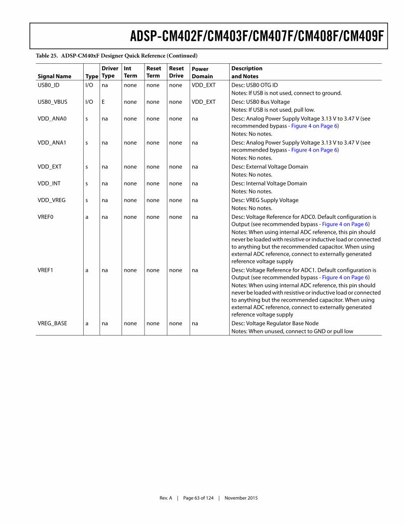
Rev. A | Page 63 of 124 | November 2015
ADSP-CM402F/CM403F/CM407F/CM408F/CM409F
USB0_ID I/O na none none none VDD_EXT Desc: USB0 OTG IDNotes: If USB is not used, connect to ground.
USB0_VBUS I/O E none none none VDD_EXT Desc: USB0 Bus VoltageNotes: If USB is not used, pull low.
VDD_ANA0 s na none none none na Desc: Analog Power Supply Voltage 3.13 V to 3.47 V (see recommended bypass - Figure 4 on Page 6)Notes: No notes.
VDD_ANA1 s na none none none na Desc: Analog Power Supply Voltage 3.13 V to 3.47 V (see recommended bypass - Figure 4 on Page 6)Notes: No notes.
VDD_EXT s na none none none na Desc: External Voltage DomainNotes: No notes.
VDD_INT s na none none none na Desc: Internal Voltage DomainNotes: No notes.
VDD_VREG s na none none none na Desc: VREG Supply VoltageNotes: No notes.
VREF0 a na none none none na Desc: Voltage Reference for ADC0. Default configuration is Output (see recommended bypass - Figure 4 on Page 6)Notes: When using internal ADC reference, this pin should never be loaded with resistive or inductive load or connected to anything but the recommended capacitor. When using external ADC reference, connect to externally generated reference voltage supply
VREF1 a na none none none na Desc: Voltage Reference for ADC1. Default configuration is Output (see recommended bypass - Figure 4 on Page 6)Notes: When using internal ADC reference, this pin should never be loaded with resistive or inductive load or connected to anything but the recommended capacitor. When using external ADC reference, connect to externally generated reference voltage supply
VREG_BASE a na none none none na Desc: Voltage Regulator Base NodeNotes: When unused, connect to GND or pull low
Table 25. ADSP-CM40xF Designer Quick Reference (Continued)
Signal Name TypeDriver Type
Int Term
Reset Term
Reset Drive
Power Domain
Descriptionand Notes
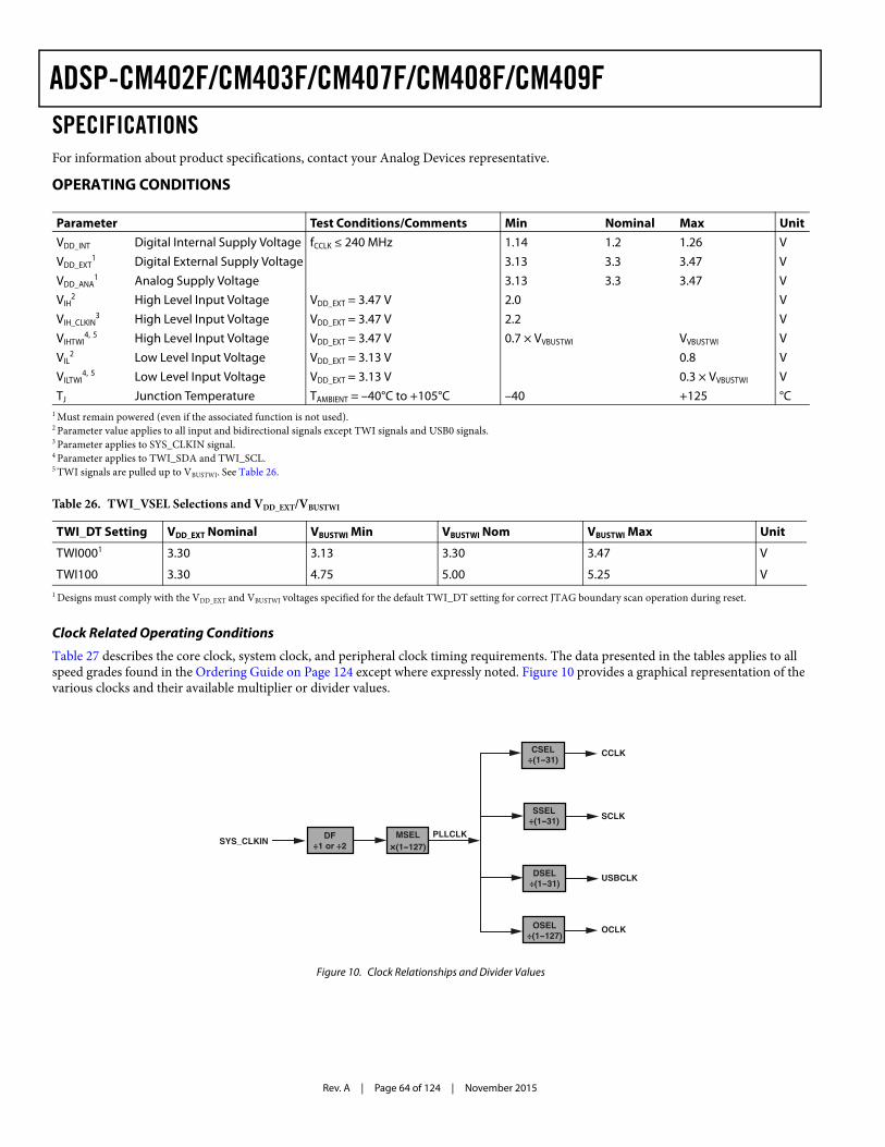
Rev. A | Page 64 of 124 | November 2015
ADSP-CM402F/CM403F/CM407F/CM408F/CM409FSPECIFICATIONSFor information about product specifications, contact your Analog Devices representative.
OPERATING CONDITIONS
Clock Related Operating Conditions
Table 27 describes the core clock, system clock, and peripheral clock timing requirements. The data presented in the tables applies to all speed grades found in the Ordering Guide on Page 124 except where expressly noted. Figure 10 provides a graphical representation of the various clocks and their available multiplier or divider values.
Parameter Test Conditions/Comments Min Nominal Max UnitVDD_INT Digital Internal Supply Voltage fCCLK ≤ 240 MHz 1.14 1.2 1.26 VVDD_EXT
1
1 Must remain powered (even if the associated function is not used).
Digital External Supply Voltage 3.13 3.3 3.47 VVDD_ANA
1 Analog Supply Voltage 3.13 3.3 3.47 VVIH
2
2 Parameter value applies to all input and bidirectional signals except TWI signals and USB0 signals.
High Level Input Voltage VDD_EXT = 3.47 V 2.0 VVIH_CLKIN
3
3 Parameter applies to SYS_CLKIN signal.
High Level Input Voltage VDD_EXT = 3.47 V 2.2 VVIHTWI
4, 5
4 Parameter applies to TWI_SDA and TWI_SCL.5 TWI signals are pulled up to VBUSTWI. See Table 26.
High Level Input Voltage VDD_EXT = 3.47 V 0.7 × VVBUSTWI VVBUSTWI VVIL
2 Low Level Input Voltage VDD_EXT = 3.13 V 0.8 VVILTWI
4, 5 Low Level Input Voltage VDD_EXT = 3.13 V 0.3 × VVBUSTWI VTJ Junction Temperature TAMBIENT = –40°C to +105°C –40 +125 °C
Table 26. TWI_VSEL Selections and VDD_EXT/VBUSTWI
TWI_DT Setting VDD_EXT Nominal VBUSTWI Min VBUSTWI Nom VBUSTWI Max Unit
TWI0001
1 Designs must comply with the VDD_EXT and VBUSTWI voltages specified for the default TWI_DT setting for correct JTAG boundary scan operation during reset.
3.30 3.13 3.30 3.47 V
TWI100 3.30 4.75 5.00 5.25 V
Figure 10. Clock Relationships and Divider Values
SYS_CLKIN
USBCLK
SCLK
CCLKCSEL÷(1-31)
SSEL÷(1-31)
DSEL÷(1-31)
OCLKOSEL÷(1-127)
PLLCLKMSEL×(1-127)
DF÷1 or ÷2
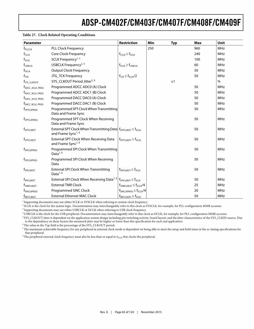
Rev. A | Page 65 of 124 | November 2015
ADSP-CM402F/CM403F/CM407F/CM408F/CM409FTable 27. Clock Related Operating Conditions
Parameter Restriction Min Typ Max UnitfPLLCLK PLL Clock Frequency 250 960 MHzfCCLK Core Clock Frequency fCCLK fSCLK 240 MHzfSCLK SCLK Frequency1, 2 100 MHzfUSBCLK USBCLK Frequency3, 4 fSCLK fUSBCLK 60 MHzfOCLK Output Clock Frequency 50 MHzfTCK JTG_TCK Frequency fTCK fSCLK/2 50 MHzfSYS_CLKOUTJ SYS_CLKOUT Period Jitter5, 6 ±1 %fADCC_ACLK_PROG Programmed ADCC ADC0 (A) Clock 50 MHzfADCC_BCLK_PROG Programmed ADCC ADC1 (B) Clock 50 MHzfDACC_ACLK_PROG Programmed DACC DAC0 (A) Clock 50 MHzfDACC_BCLK_PROG Programmed DACC DAC1 (B) Clock 50 MHzfSPTCLKPROG Programmed SPT Clock When Transmitting
Data and Frame Sync 50 MHz
fSPTCLKPROG Programmed SPT Clock When Receiving Data and Frame Sync
50 MHz
fSPTCLKEXT External SPT Clock When Transmitting Data and Frame Sync7, 8
fSPTCLKEXT fSCLK 50 MHz
fSPTCLKEXT External SPT Clock When Receiving Data and Frame Sync7, 8
fSPTCLKEXT fSCLK 50 MHz
fSPICLKPROG Programmed SPI Clock When Transmitting Data7, 8
50 MHz
fSPICLKPROG Programmed SPI Clock When Receiving Data
50 MHz
fSPICLKEXT External SPI Clock When Transmitting Data7, 8
fSPICLKEXT fSCLK 50 MHz
fSPICLKEXT External SPI Clock When Receiving Data7, 8 fSPICLKEXT fSCLK 50 MHzfTMRCLKEXT External TMR Clock fTMRCLKEXT fSCLK/4 25 MHzfSINCLKPROG Programmed SINC Clock fSINCLKPROG fSCLK/4 20 MHzfREFCLKEXT External Ethernet MAC Clock fREFCLKEXT fSCLK 50 MHz
1 Supporting documents may use either SCLK or SYSCLK when referring to system clock frequency.2 SCLK is the clock for the system logic. Documentation may interchangeably refer to this clock as SYSCLK, for example, for PLL configuration MMR accesses.3 Supporting documents may use either USBCLK or DCLK when referring to USB clock frequency.4 USBCLK is the clock for the USB peripheral. Documentation may interchangeably refer to this clock as DCLK, for example, for PLL configuration MMR accesses.5 SYS_CLKOUT jitter is dependent on the application system design including pin switching activity, board layout, and the jitter characteristics of the SYS_CLKIN source. Due
to the dependency on these factors the measured jitter may be higher or lower than this specification for each end application.6 The value in the Typ field is the percentage of the SYS_CLKOUT period.7 The maximum achievable frequency for any peripheral in external clock mode is dependent on being able to meet the setup and hold times in the ac timing specifications for
that peripheral.8 The peripheral external clock frequency must also be less than or equal to fSCLK that clocks the peripheral.
Rev. A | Page 66 of 124 | November 2015
ADSP-CM402F/CM403F/CM407F/CM408F/CM409FELECTRICAL CHARACTERISTICS
Parameter Test Conditions/Comments Min Typ Max Unit
VOH1
1 Applies to all output and bidirectional signals except TWI signals and USB0 signals.
High Level Output Voltage VDD_EXT = 3.13 V, IOH = –0.5 mA 2.4 V
VOL2
2 Applies to all output and bidirectional signals except USB0 signals.
Low Level Output Voltage VDD_EXT = 3.13 V, IOL = 2.0 mA 0.4 V
IIH3
3 Applies to input pins.
High Level Input Current VDD_EXT =3.47 V, VIN = 3.47 V 10 μA
IIL3 Low Level Input Current VDD_EXT =3.47 V, VIN = 0 V 10 μA
IIH_PD4
4 Applies to signal JTG_TCK.
High Level Input Current With Pull-down Resistor
VDD_EXT = 3.47 V, VIN = 3.47 V 25 100 μA
IIL_PU5
5 Applies to signals JTG_TMS, JTG_TRST, and JTAG_TDI.
Low Level Input Current With Pull-up Resistor
VDD_EXT = 3.47 V, VIN = 0 V 25 100 μA
IIL_USB06
6 Applies to signals USB0_DM and USB0_VBUS.
Low Level Input Current VDD_EXT = 3.47 V, VIN = 0 V 200 μA
IOZH7
7 Applies to three-statable pins.
Three-State Leakage Current VDD_EXT = 3.47 V, VIN = 3.47 V 10 μA
IOZL_PU8
8 Applies to all GPIO pins when pull-up resistors are enabled.
Three-State Leakage Current With Pull-up Resistor
VDD_EXT = 3.47 V, VIN = 0 V 25 100 μA
IOZHTWI9
9 Applies to all TWI signals.
Three-State Leakage Current VDD_EXT =3.47 V, VIN = 5.5 V 10 μA
IOZL7 Three-State Leakage Current VDD_EXT = 3.47 V, VIN = 0 V 10 μA
CIN10
10Applies to all signals except TWI signals.
Input Capacitance TJ = 25°C 4.2 5.2 pF
CIN_TWI9 Input Capacitance TJ = 25°C 8.3 8.6 pF
IDDINT_STATIC VDD_INT Static Current fCCLK = 0 MHzfSCLK = 0 MHz
See Figure 11 on Page 67
mA
IDD_IDLE VDD_INT Current in Idle fCCLK = 200 MHzASF = 0.31 (idle), fSCLK = 100 MHzNo DMA activity TJ = 25°C
59 mA
IDD_TYP VDD_INT Current fCCLK = 200 MHz ASF = 1.0 (typical),fSCLK = 100 MHzDMA data rate = 100 MB/sTJ = 25°C
97 mA
IDD_TYP VDD_INT Current fCCLK = 240 MHz ASF = 1.0 (typical),fSCLK = 96 MHzDMA data rate = 100 MB/s TJ = 25°C
104 mA
IDD_INT VDD_INT Current fCCLK 0 MHz fSCLK 0 MHz
See IDDINT_TOT equation
mA
IDD_EXT VDD_EXT Current See IDDEXT_TOT equation
mA
IDD_ANA VDD_ANA0 + VDD_ANA1 Current 60 70 mA
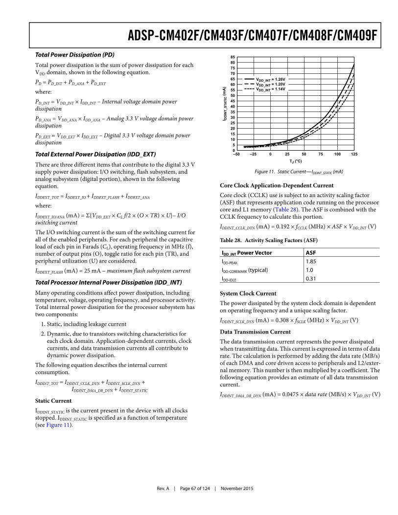
Rev. A | Page 67 of 124 | November 2015
ADSP-CM402F/CM403F/CM407F/CM408F/CM409FTotal Power Dissipation (PD)
Total power dissipation is the sum of power dissipation for each VDD domain, shown in the following equation.PD = PD_INT + PD_ANA + PD_EXT
where:PD_INT = VDD_INT × IDD_INT – Internal voltage domain power dissipationPD_ANA = VDD_ANA × IDD_ANA – Analog 3.3 V voltage domain power dissipationPD_EXT = VDD_EXT × IDD_EXT – Digital 3.3 V voltage domain power dissipation
Total External Power Dissipation (IDD_EXT)
There are three different items that contribute to the digital 3.3 V supply power dissipation: I/O switching, flash subsystem, and analog subsystem (digital portion), shown in the following equation.IDDEXT_TOT = IDDEXT_IO + IDDEXT_FLASH + IDDEXT_ANA where:IDDEXT_IO/ANA (mA) = Σ{VDD_EXT × CL f/2 × (O × TR) × U}– I/O switching currentThe I/O switching current is the sum of the switching current for all of the enabled peripherals. For each peripheral the capacitive load of each pin in Farads (CL), operating frequency in MHz (f), number of output pins (O), toggle ratio for each pin (TR), and peripheral utilization (U) are considered.IDDEXT_FLASH (mA) = 25 mA – maximum flash subsystem current
Total Processor Internal Power Dissipation (IDD_INT)
Many operating conditions affect power dissipation, including temperature, voltage, operating frequency, and processor activity. Total internal power dissipation for the processor subsystem has two components:
1. Static, including leakage current2. Dynamic, due to transistors switching characteristics for
each clock domain. Application-dependent currents, clock currents, and data transmission currents all contribute to dynamic power dissipation.
The following equation describes the internal current consumption.IDDINT_TOT = IDDINT_CCLK_DYN + IDDINT_SCLK_DYN +
IDDINT_DMA_DR_DYN + IDDINT_STATIC
Static CurrentIDDINT_STATIC is the current present in the device with all clocks stopped. IDDINT_STATIC is specified as a function of temperature (see Figure 11).
Core Clock Application-Dependent CurrentCore clock (CCLK) use is subject to an activity scaling factor (ASF) that represents application code running on the processor core and L1 memory (Table 28). The ASF is combined with the CCLK frequency to calculate this portion.IDDINT_CCLK_DYN (mA) = 0.192 × fCCLK (MHz) × ASF × VDD_INT (V)
System Clock CurrentThe power dissipated by the system clock domain is dependent on operating frequency and a unique scaling factor.IDDINT_SCLK_DYN (mA) = 0.308 × fSCLK (MHz) × VDD_INT (V)
Data Transmission CurrentThe data transmission current represents the power dissipated when transmitting data. This current is expressed in terms of data rate. The calculation is performed by adding the data rate (MB/s) of each DMA and core driven access to peripherals and L2/exter-nal memory. This number is then multiplied by a coefficient. The following equation provides an estimate of all data transmission current.IDDINT_DMA_DR_DYN (mA) = 0.0475 × data rate (MB/s) × VDD_INT (V)
Figure 11. Static Current—IDDINT_STATIC (mA)
Table 28. Activity Scaling Factors (ASF)
IDD_INT Power Vector ASFIDD-PEAK 1.85IDD-COREMARK (typical) 1.0IDD-IDLE 0.31
05
10152025303540455055606570758085
–50 –25 0 25 50 75 100 125
I DD
INT_
STAT
IC (m
A)
TJ (°C)
VDD_INT = 1.14VVDD_INT = 1.20VVDD_INT = 1.26V
Rev. A | Page 68 of 124 | November 2015
ADSP-CM402F/CM403F/CM407F/CM408F/CM409FADC/DAC SPECIFICATIONS
ADC Specifications
Typical values assume VDD_ANA = 3.3 V, VREF = 2.5 V.
Parameter Min Typ Max Unit Test Conditions/CommentsANALOG INPUT ADC0_VIN, 00–11, ADC1_VIN, 00–11
Requirement Single-Ended Input Voltage Range 0 2.5 2.75 V For input voltage >2.5 V, must use external
voltage reference (input mode)Characteristic DC Leakage Current ±1 μA Input Resistance 85 Ω See Figure 5 on Page 6 Input Capacitance 9.0 pF Condition 1 = track, See Figure 5 on Page 6
1.5 pF Condition 2 = hold, includes all parasitic capacitances, See Figure 5 on Page 6
VOLTAGE REFERENCE (OUTPUT MODE)
VREF0, VREF1
Characteristic Output Voltage 2.5 ± 0.25% V Output Voltage Thermal Hysteresis 50 ppm Output Impedance 0.5 1.0 Ω Temperature Coefficient 20 ppm/°C TJ = –40°C to +125°C VOLTAGE REFERENCE (INPUT MODE) VREF0, VREF1
Requirement Input Voltage Range 0 2.5 2.75 V Requires 750 μA capable source current DC Leakage Current 300 μA Input Capacitance 0.6 pFSTATIC PERFORMANCEDC ACCURACY ADC0_VIN, 00–11, ADC1_VIN, 00–11
Characteristic Resolution 16 Bits No missing codes, natural binary codingADSP-CM403F/ADSP-CM408F/ADSP-CM409F Differential Nonlinearity (DNL) –0.99 +1.5 LSB See Figure 12 on Page 71 Integral Nonlinearity (INL) ±3.0 ±5.0 LSB Offset Error ±5.0 ±10 LSB Offset Error Match ±2.0 LSB Channel-to-channel, within one ADC Offset Drift ±2.0 ppm/°C Gain Error ±32 ±250 LSB Gain Error Match ±2.0 LSBADSP-CM402F/ADSP-CM407F Differential Nonlinearity (DNL) –0.99 +2.0 LSB See Figure 12 on Page 71 Integral Nonlinearity (INL) ±10.0 ±12.0 LSB Offset Error ±10.0 ±12.0 LSB Offset Error Match ±2.0 LSB Channel-to-channel, within one ADC Offset Drift ±2.0 ppm/°C Gain Error ±64 ±300 LSB Gain Error Match ±2.0 LSB
Rev. A | Page 69 of 124 | November 2015
ADSP-CM402F/CM403F/CM407F/CM408F/CM409F
DYNAMIC PERFORMANCEThroughput ADC0_VIN, 00–11, ADC1_VIN, 00–11
Conversion Rate 2.63 MSPS Acquisition time 150 nsAC ACCURACY ADC0_VIN, 00–11, ADC1_VIN, 00–11
CharacteristicADSP-CM403F/ADSP-CM408F/ADSP-CM409F Signal-to-Noise Ratio (SNR)1 80.25 81.25 dB Signal-to-(Noise + Distortion) Ratio (SINAD)1
80 81 dB
Total Harmonic Distortion (THD)1 –92 dB Spurious-Free Dynamic Range (SFDR)1
90 dBc
Dynamic Range 82 83 dB VIN = VREF/2 (dc) Effective Number of Bits (ENOB) 13.0 13.2 BitsADSP-CM402F/ADSP-CM407F Signal-to-Noise Ratio (SNR)1 73 74 dB Signal-to-(Noise + Distortion) Ratio (SINAD)1
72 73 dB
Total Harmonic Distortion (THD)1 –88 dB Spurious-Free Dynamic Range (SFDR)1
88 dBc
Dynamic Range 74.5 75.5 dB VIN = VREF/2 (dc) Effective Number of Bits (ENOB) 11.6 11.8 BitsChannel-to-Channel Isolation –95 dB Any channel pair referenced on same ADC
Selected channel = 1 kHz, unselected channel = 10 kHz
ADC-to-ADC Isolation –100 dB Any channel pair referenced on opposite ADC
1 fIN = 1 kHz, 0 V to 2.5 V input, 2.63 MSPS.
Parameter Min Typ Max Unit Test Conditions/Comments
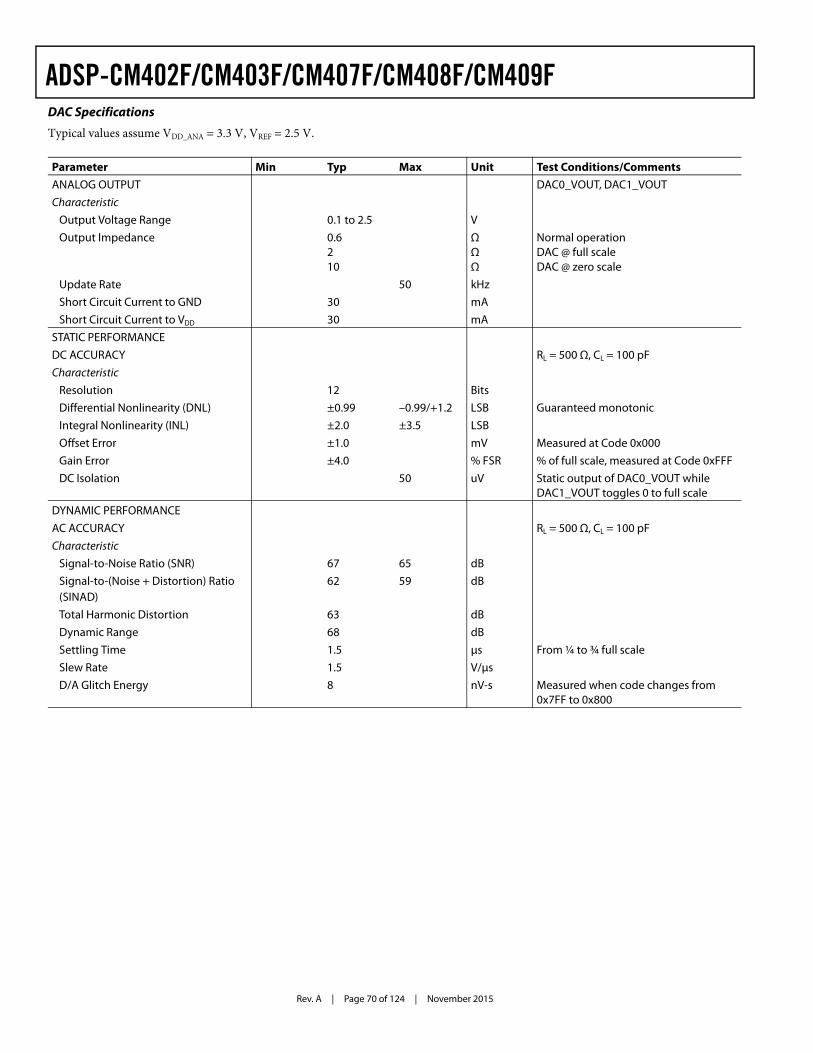
Rev. A | Page 70 of 124 | November 2015
ADSP-CM402F/CM403F/CM407F/CM408F/CM409FDAC Specifications
Typical values assume VDD_ANA = 3.3 V, VREF = 2.5 V.
Parameter Min Typ Max Unit Test Conditions/CommentsANALOG OUTPUT DAC0_VOUT, DAC1_VOUTCharacteristic Output Voltage Range 0.1 to 2.5 V Output Impedance 0.6
210
ΩΩΩ
Normal operationDAC @ full scaleDAC @ zero scale
Update Rate 50 kHz Short Circuit Current to GND 30 mA Short Circuit Current to VDD 30 mASTATIC PERFORMANCEDC ACCURACY RL = 500 Ω, CL = 100 pFCharacteristic Resolution 12 Bits Differential Nonlinearity (DNL) ±0.99 –0.99/+1.2 LSB Guaranteed monotonic Integral Nonlinearity (INL) ±2.0 ±3.5 LSB Offset Error ±1.0 mV Measured at Code 0x000 Gain Error ±4.0 % FSR % of full scale, measured at Code 0xFFF DC Isolation 50 uV Static output of DAC0_VOUT while
DAC1_VOUT toggles 0 to full scaleDYNAMIC PERFORMANCEAC ACCURACY RL = 500 Ω, CL = 100 pFCharacteristic Signal-to-Noise Ratio (SNR) 67 65 dB Signal-to-(Noise + Distortion) Ratio (SINAD)
62 59 dB
Total Harmonic Distortion 63 dB Dynamic Range 68 dB Settling Time 1.5 μs From ¼ to ¾ full scale Slew Rate 1.5 V/μs D/A Glitch Energy 8 nV-s Measured when code changes from
0x7FF to 0x800
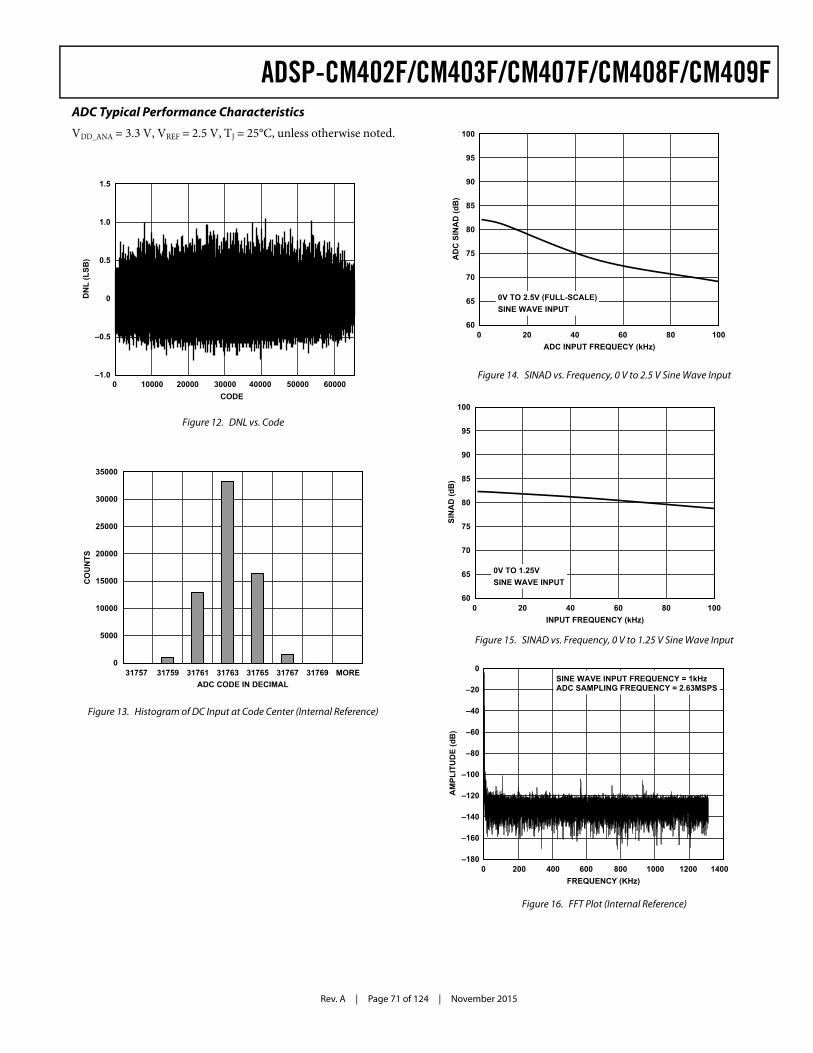
Rev. A | Page 71 of 124 | November 2015
ADSP-CM402F/CM403F/CM407F/CM408F/CM409FADC Typical Performance Characteristics
VDD_ANA = 3.3 V, VREF = 2.5 V, TJ = 25°C, unless otherwise noted.
Figure 12. DNL vs. Code
Figure 13. Histogram of DC Input at Code Center (Internal Reference)
–1.0
–0.5
0
0.5
1.0
1.5
100000 20000 30000 40000 50000 60000
DN
L (L
SB)
CODE
0
5000
10000
15000
20000
25000
30000
35000
31757 31759 31761 31763 31765 31767 31769 MORE
CO
UN
TS
ADC CODE IN DECIMAL
Figure 14. SINAD vs. Frequency, 0 V to 2.5 V Sine Wave Input
Figure 15. SINAD vs. Frequency, 0 V to 1.25 V Sine Wave Input
Figure 16. FFT Plot (Internal Reference)
60
65
70
75
80
85
90
95
100
0 20 40 60 80 100
AD
C S
INA
D (d
B)
ADC INPUT FREQUECY (kHz)
0V TO 2.5V (FULL-SCALE)SINE WAVE INPUT
60
65
70
75
80
85
90
95
100
0 20 40 60 80 100
SIN
AD
(dB
)
INPUT FREQUENCY (kHz)
0V TO 1.25V SINE WAVE INPUT
–180
–160
–140
–120
–100
–80
–60
–40
–20
0
0 200 600400 800 1000 1200 1400
AM
PLIT
UD
E (d
B)
FREQUENCY (KHz)
SINE WAVE INPUT FREQUENCY = 1kHzADC SAMPLING FREQUENCY = 2.63MSPS
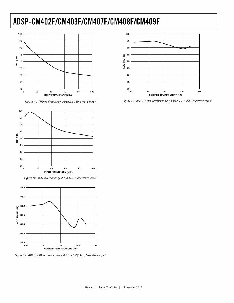
Rev. A | Page 72 of 124 | November 2015
ADSP-CM402F/CM403F/CM407F/CM408F/CM409F
Figure 17. THD vs. Frequency, 0 V to 2.5 V Sine Wave Input
Figure 18. THD vs. Frequency, 0 V to 1.25 V Sine Wave Input
Figure 19. ADC SINAD vs. Temperature, 0 V to 2.5 V (1 kHz) Sine Wave Input
60
65
70
75
80
85
90
95
100
0 20 40 60 80 100
THD
(dB
)
INPUT FREQUENCY (kHz)
60
65
70
75
80
85
90
95
100
0 20 40 60 80 100
THD
(dB
)
INPUT FREQUENCY (kHz)
80.0
80.5
81.0
81.5
82.0
82.5
83.0
–50 0 50 100 150
AD
C S
INA
D (d
B)
AMBIENT TEMPERATURE (° C)
Figure 20. ADC THD vs. Temperature, 0 V to 2.5 V (1 kHz) Sine Wave Input
60
65
70
75
80
85
90
95
100
–50 0 50 100 150
AD
C T
HD
(dB
)
AMBIENT TEMPERATURE (°C)
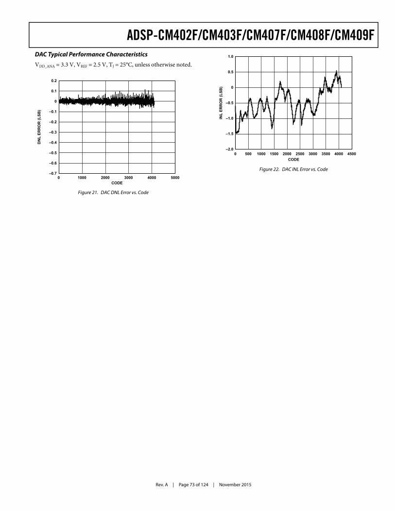
Rev. A | Page 73 of 124 | November 2015
ADSP-CM402F/CM403F/CM407F/CM408F/CM409FDAC Typical Performance Characteristics
VDD_ANA = 3.3 V, VREF = 2.5 V, TJ = 25°C, unless otherwise noted.
Figure 21. DAC DNL Error vs. Code
–0.7
–0.6
–0.5
–0.4
–0.3
–0.2
–0.1
0
0.1
0.2
0 1000 2000 3000CODE
DN
L ER
RO
R (L
SB)
4000 5000
Figure 22. DAC INL Error vs. Code
–2.0
–1.5
–1.0
–0.5
0
0.5
1.0
0 500 1000 1500 2000CODE
INL
ERR
OR
(LSB
)
2500 3000 3500 4000 4500
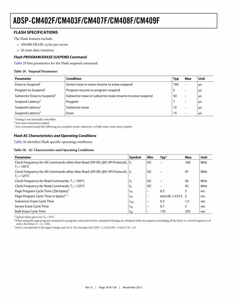
Rev. A | Page 74 of 124 | November 2015
ADSP-CM402F/CM403F/CM407F/CM408F/CM409FFLASH SPECIFICATIONSThe Flash features include:
• 100,000 ERASE cycles per sector• 20 years data retention
Flash PROGRAM/ERASE SUSPEND Command
Table 29 lists parameters for the Flash suspend command.
Flash AC Characteristics and Operating Conditions
Table 30 identifies Flash specific operating conditions.
Table 29. Suspend Parameters
Parameter Condition Typ Max Unit
Erase to Suspend1
1 Timing is not internally controlled.
Sector erase or erase resume to erase suspend 700 – μs
Program to Suspend1 Program resume to program suspend 5 – μs
Subsector Erase to Suspend1 Subsector erase or subsector erase resume to erase suspend 50 – μs
Suspend Latency2
2 Any read command accepted.
Program 7 – μs
Suspend Latency2 Subsector erase 15 – μs
Suspend Latency3
3 Any command except the following are accepted: sector, subsector, or bulk erase; write status register.
Erase 15 – μs
Table 30. AC Characteristics and Operating Conditions
Parameter Symbol Min Typ1
1 Typical values given for TJ = 25°C.
Max UnitClock Frequency for All Commands other than Read (SPI-ER, QIO-SPI Protocol), TJ = 105°C
fC DC – 100 MHz
Clock Frequency for All Commands other than Read (SPI-ER, QIO-SPI Protocol), TJ = 125°C
fC DC – 97 MHz
Clock Frequency for Read Commands, TJ = 105°C fR DC – 50 MHzClock Frequency for Read Commands, TJ = 125°C fR DC – 45 MHzPage Program Cycle Time (256 bytes)2
2 When using the page program command to program consecutive bytes, optimized timings are obtained with one sequence including all the bytes vs. several sequences of only a few bytes (1 < n < 256).
tPP – 0.5 5 msPage Program Cycle Time (n bytes)2, 3
3 int(A) corresponds to the upper integer part of A. For example int(12/8) = 2, int(32/8) = 4 int(15.3) = 16.
tPP – int(n/8) × 0.015 5 msSubsector Erase Cycle Time tSSE – 0.3 1.5 secSector Erase Cycle Time tSE – 0.7 3 secBulk Erase Cycle Time tBE – 170 250 sec
Rev. A | Page 75 of 124 | November 2015
ADSP-CM402F/CM403F/CM407F/CM408F/CM409FABSOLUTE MAXIMUM RATINGSStresses at or above those listed in Table 31 may cause perma-nent damage to the product. This is a stress rating only; functional operation of the product at these or any other condi-tions above those indicated in the operational section of this specification is not implied. Operation beyond the maximum operating conditions for extended periods may affect product reliability.
ESD SENSITIVITY
PACKAGE INFORMATIONThe information presented in Figure 23 and Table 33 provides details about package branding. For a complete listing of prod-uct availability, see Ordering Guide on Page 124.
Table 31. Absolute Maximum Ratings
Parameter RatingInternal Supply Voltage (VDD_INT) –0.33 V to +1.32 VExternal (I/O) Supply Voltage (VDD_EXT) –0.33 V to +3.63 VAnalog Supply Voltage (VDD_ANA) –0.33 V to +3.63 VDigital Input Voltage1, 2
1 Applies to 100% transient duty cycle. For other duty cycles, see Table 32. 2 Applies only when VDD_EXT is within specifications. When VDD_EXT is outside speci-
fications, the range is VDD_EXT ± 0.2 V.
–0.33 V to +3.63 VTWI Digital Input Voltage1, 2, 3
3 Applies to pins TWI_SCL and TWI_SDA.
–0.33 V to +5.50 VDigital Output Voltage Swing –0.33 V to VDD_EXT + 0.5 VAnalog Input Voltage4
4 Applies only when VDD_ANA is within specification. When VDD_ANA is outside speci-fications, the range is VDD_ANA ± 0.2 V.
–0.33 V to +3.63 VVoltage Reference Input Voltage (VREF0, VREF1)4
–0.33 V to +2.75 V
USB0_Dx Input –0.33 V to +5.25 VUSB0_VBUS Input Voltage –0.33 V to +6.00 VIOH/IOL Current per Signal1 6 mA (max)Storage Temperature Range –65°C to +150°CJunction Temperature While Biased +125°C
Table 32. Maximum Duty Cycle for Input Transient Voltage1
1 Applies to all signal pins with the exception of SYS_CLKIN, SYS_XTAL, USB0_DP, USB0_DM, USB0_VBUS, and TWI signals.
Maximum Duty Cycle (%)2
2 Applies only when VDD_EXT is within specifications. When VDD_EXT is outside specifications, the range is VDD_EXT ± 0.2 V.
VIN Min (V)3
3 The individual values cannot be combined for analysis of a single instance of overshoot or undershoot. The worst case observed value must fall within one of the specified voltages, and the total duration of the overshoot or undershoot (exceeding the 100% case) must be less than or equal to the corresponding duty cycle.
VIN Max (V)3
100 –0.33 +3.6350 –0.46 +3.7840 –0.52 +3.8525 –0.63 +3.9620 –0.67 +3.9915 –0.70 +4.0310 –0.73 +4.07
Figure 23. Product Information on Package1
1 Exact brand may differ, depending on package type.
Table 33. Package Brand Information
Brand Key Field DescriptionADSP-CM40xF Product modelt Temperature rangepp Package typeZ RoHS compliant designationcc See Ordering Guidevvvvvv.x Assembly lot coden Silicon revisionyyww Date code
ESD (electrostatic discharge) sensitive device.Charged devices and circuit boards can discharge without detection. Although this product features patented or proprietary protection circuitry, damage may occur on devices subjected to high energy ESD. Therefore, proper ESD precautions should be taken to avoid performance degradation or loss of functionality.
ADSP-CM40xF
a
#yyww country_of_origin
vvvvvv.x-n
tppZ-cc
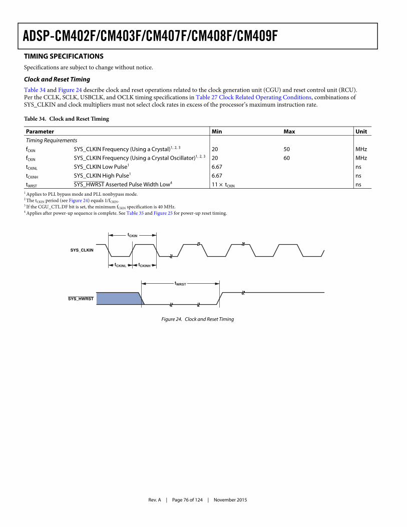
Rev. A | Page 76 of 124 | November 2015
ADSP-CM402F/CM403F/CM407F/CM408F/CM409FTIMING SPECIFICATIONSSpecifications are subject to change without notice.
Clock and Reset Timing
Table 34 and Figure 24 describe clock and reset operations related to the clock generation unit (CGU) and reset control unit (RCU). Per the CCLK, SCLK, USBCLK, and OCLK timing specifications in Table 27 Clock Related Operating Conditions, combinations of SYS_CLKIN and clock multipliers must not select clock rates in excess of the processor’s maximum instruction rate.
Table 34. Clock and Reset Timing
Parameter Min Max UnitTiming RequirementsfCKIN SYS_CLKIN Frequency (Using a Crystal)1, 2, 3
1 Applies to PLL bypass mode and PLL nonbypass mode.2 The tCKIN period (see Figure 24) equals 1/fCKIN.3 If the CGU_CTL.DF bit is set, the minimum fCKIN specification is 40 MHz.
20 50 MHzfCKIN SYS_CLKIN Frequency (Using a Crystal Oscillator)1, 2, 3 20 60 MHztCKINL SYS_CLKIN Low Pulse1 6.67 nstCKINH SYS_CLKIN High Pulse1 6.67 nstWRST SYS_HWRST Asserted Pulse Width Low4
4 Applies after power-up sequence is complete. See Table 35 and Figure 25 for power-up reset timing.
11 × tCKIN ns
Figure 24. Clock and Reset Timing
SYS_CLKIN
tWRST
tCKIN
tCKINL tCKINH
SYS_HWRST
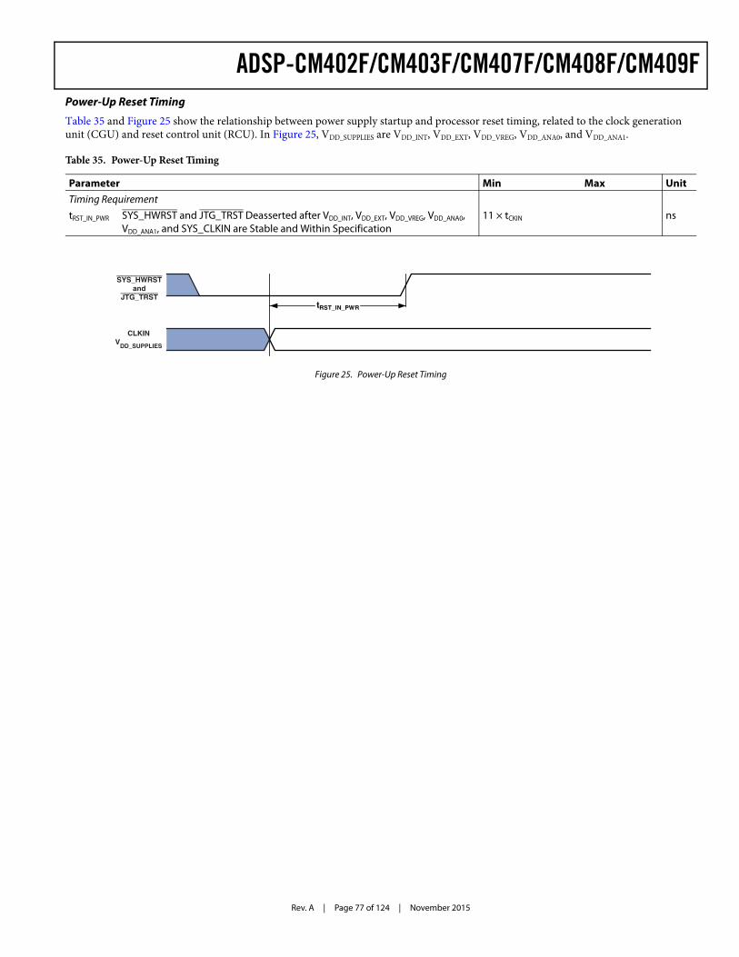
Rev. A | Page 77 of 124 | November 2015
ADSP-CM402F/CM403F/CM407F/CM408F/CM409FPower-Up Reset Timing
Table 35 and Figure 25 show the relationship between power supply startup and processor reset timing, related to the clock generation unit (CGU) and reset control unit (RCU). In Figure 25, VDD_SUPPLIES are VDD_INT, VDD_EXT, VDD_VREG, VDD_ANA0, and VDD_ANA1.
Table 35. Power-Up Reset Timing
Parameter Min Max UnitTiming RequirementtRST_IN_PWR SYS_HWRST and JTG_TRST Deasserted after VDD_INT, VDD_EXT, VDD_VREG, VDD_ANA0,
VDD_ANA1, and SYS_CLKIN are Stable and Within Specification11 × tCKIN ns
Figure 25. Power-Up Reset Timing
tRST_IN_PWR
CLKINV
DD_SUPPLIES
SYS_HWRSTand
JTG_TRST
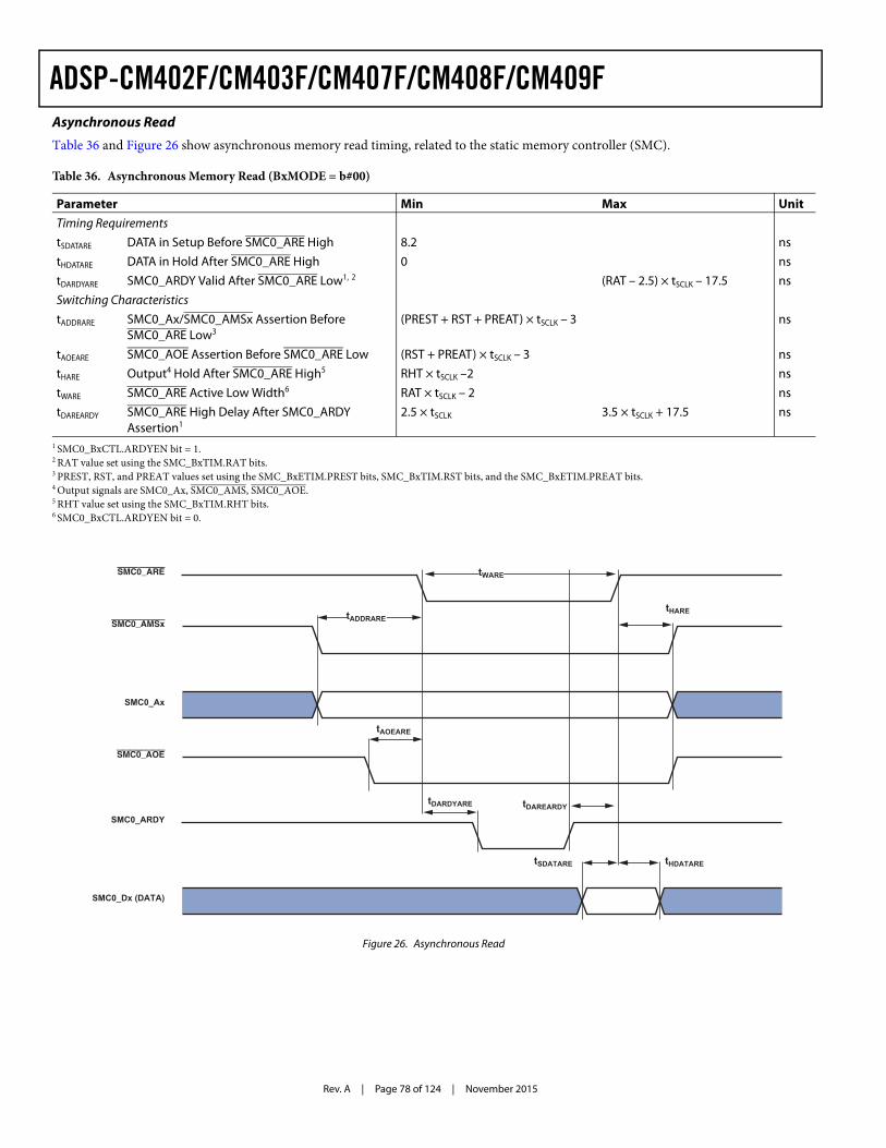
Rev. A | Page 78 of 124 | November 2015
ADSP-CM402F/CM403F/CM407F/CM408F/CM409FAsynchronous Read
Table 36 and Figure 26 show asynchronous memory read timing, related to the static memory controller (SMC).
Table 36. Asynchronous Memory Read (BxMODE = b#00)
Parameter Min Max UnitTiming RequirementstSDATARE DATA in Setup Before SMC0_ARE High 8.2 ns tHDATARE DATA in Hold After SMC0_ARE High 0 ns tDARDYARE SMC0_ARDY Valid After SMC0_ARE Low1, 2
1 SMC0_BxCTL.ARDYEN bit = 1.2 RAT value set using the SMC_BxTIM.RAT bits.
(RAT – 2.5) × tSCLK – 17.5 nsSwitching CharacteristicstADDRARE SMC0_Ax/SMC0_AMSx Assertion Before
SMC0_ARE Low3
3 PREST, RST, and PREAT values set using the SMC_BxETIM.PREST bits, SMC_BxTIM.RST bits, and the SMC_BxETIM.PREAT bits.
(PREST + RST + PREAT) × tSCLK – 3 ns
tAOEARE SMC0_AOE Assertion Before SMC0_ARE Low (RST + PREAT) × tSCLK – 3 nstHARE Output4 Hold After SMC0_ARE High5
4 Output signals are SMC0_Ax, SMC0_AMS, SMC0_AOE.5 RHT value set using the SMC_BxTIM.RHT bits.
RHT × tSCLK –2 nstWARE SMC0_ARE Active Low Width6
6 SMC0_BxCTL.ARDYEN bit = 0.
RAT × tSCLK – 2 nstDAREARDY SMC0_ARE High Delay After SMC0_ARDY
Assertion12.5 × tSCLK 3.5 × tSCLK + 17.5 ns
Figure 26. Asynchronous Read
SMC0_ARE
SMC0_AMSx
SMC0_Ax
tWARE
SMC0_AOE
SMC0_Dx (DATA)
SMC0_ARDY
tAOEARE
tADDRARE
tDARDYARE
tHARE
tHDATARE
tDAREARDY
tSDATARE
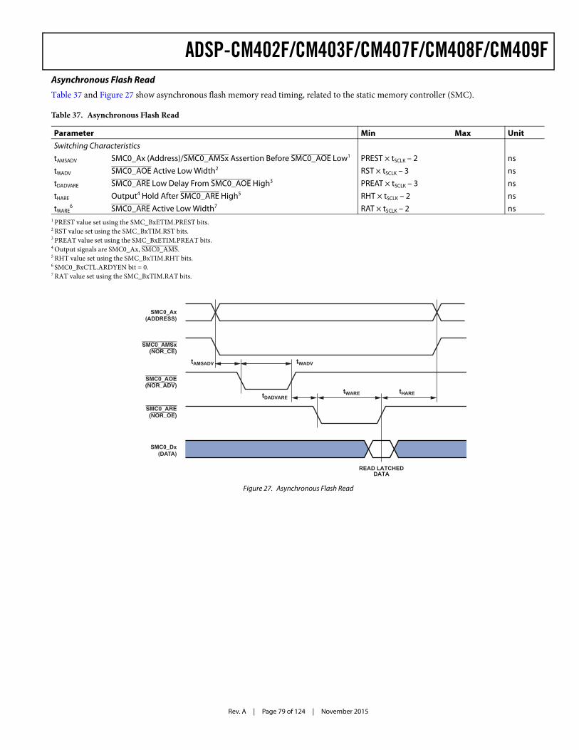
Rev. A | Page 79 of 124 | November 2015
ADSP-CM402F/CM403F/CM407F/CM408F/CM409FAsynchronous Flash Read
Table 37 and Figure 27 show asynchronous flash memory read timing, related to the static memory controller (SMC).
Table 37. Asynchronous Flash Read
Parameter Min Max UnitSwitching CharacteristicstAMSADV SMC0_Ax (Address)/SMC0_AMSx Assertion Before SMC0_AOE Low1
1 PREST value set using the SMC_BxETIM.PREST bits.
PREST × tSCLK – 2 nstWADV SMC0_AOE Active Low Width2
2 RST value set using the SMC_BxTIM.RST bits.
RST × tSCLK – 3 ns tDADVARE SMC0_ARE Low Delay From SMC0_AOE High3
3 PREAT value set using the SMC_BxETIM.PREAT bits.
PREAT × tSCLK – 3 nstHARE Output4 Hold After SMC0_ARE High5
4 Output signals are SMC0_Ax, SMC0_AMS.5 RHT value set using the SMC_BxTIM.RHT bits.
RHT × tSCLK – 2 nstWARE
6
6 SMC0_BxCTL.ARDYEN bit = 0.
SMC0_ARE Active Low Width7
7 RAT value set using the SMC_BxTIM.RAT bits.
RAT × tSCLK – 2 ns
Figure 27. Asynchronous Flash Read
SMC0_Ax(ADDRESS)
tAMSADV
tDADVARE
tWADV
tWARE tHARE
READ LATCHEDDATA
SMC0_AMSx(NOR_CE)
SMC0_AOE(NOR_ADV)
SMC0_ARE(NOR_OE)
SMC0_Dx(DATA)

Rev. A | Page 80 of 124 | November 2015
ADSP-CM402F/CM403F/CM407F/CM408F/CM409FAsynchronous Page Mode Read
Table 38 and Figure 28 show asynchronous memory page mode read timing, related to the static memory controller (SMC).
Table 38. Asynchronous Page Mode Read
Parameter Min Max UnitSwitching CharacteristicstAV SMC0_Ax (Address) Valid for First Address Min Width1
1 PREST, RST, PREAT and RAT values set using the SMC_BxETIM.PREST bits, SMC_BxTIM.RST bits, SMC_BxETIM.PREAT bits, and the SMC_BxTIM.RAT bits.
(PREST + RST + PREAT + RAT) × tSCLK – 2 ns tAV1 SMC0_Ax (Address) Valid for Subsequent SMC0_Ax
(Address) Min WidthPGWS × tSCLK – 2 ns
tWADV SMC0_AOE Active Low Width2
2 RST value set using the SMC_BxTIM.RST bits.
RST × tSCLK – 3 ns tHARE Output3 Hold After SMC0_ARE High4
3 Output signals are SMC0_Ax, SMC0_AMSx.4 RHT value set using the SMC_BxTIM.RHT bits.
RHT × tSCLK – 2 nstWARE
5
5 SMC_BxCTL.ARDYEN bit = 0.
SMC0_ARE Active Low Width6
6 RAT value set using the SMC_BxTIM.RAT bits.
RAT × tSCLK – 2 ns
Figure 28. Asynchronous Page Mode Read
SMC0_AMSx(NOR_CE)
SMC0_ARE(NOR_OE)
SMC0_AOE(NOR_ADV)
SMC0_Dx(DATA)
A0
tWADV
tWARE tHARE
D0 D1 D2 D3
A0 + 1 A0 + 2 A0 + 3
tAV tAV1 tAV1 tAV1
READ LATCHED
DATA
READ LATCHED
DATA
READ LATCHED
DATA
READ LATCHED
DATA
SMC0_Ax(ADDRESS)
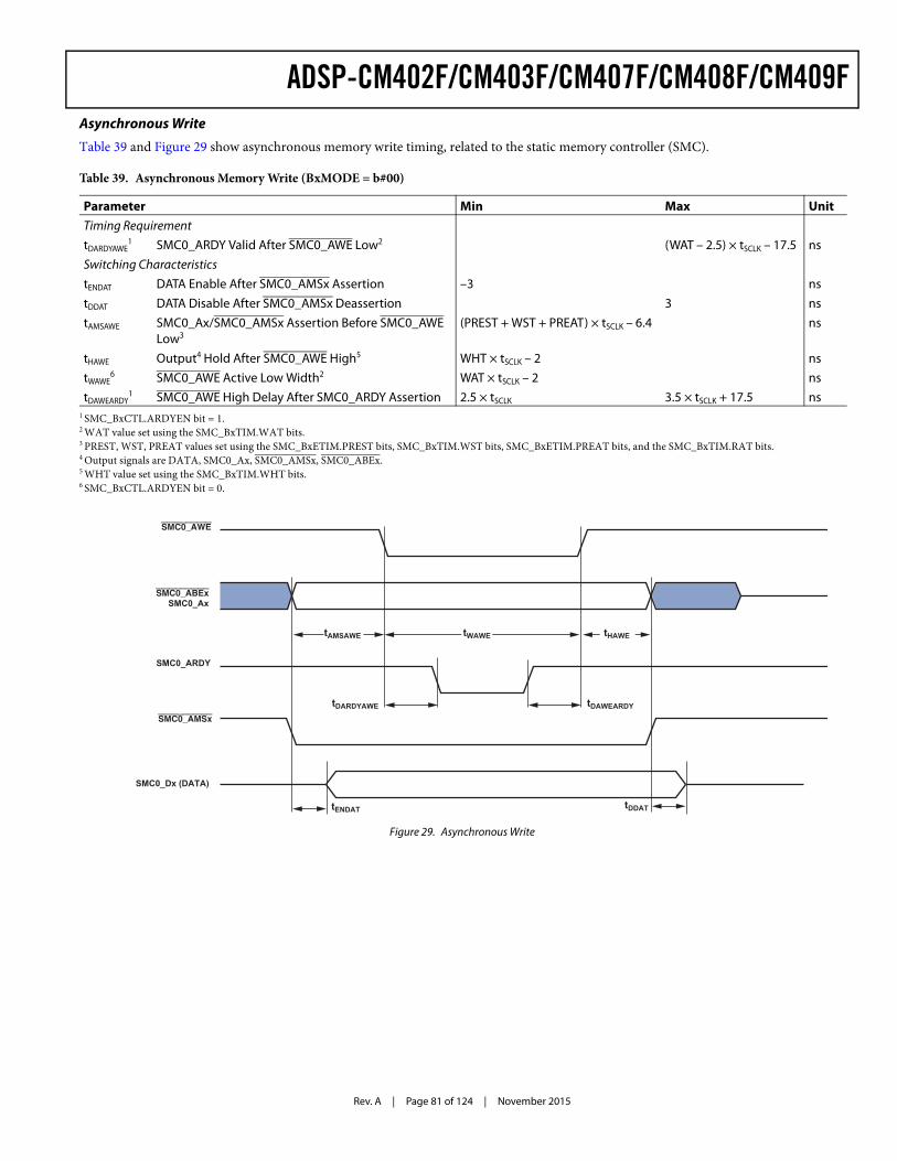
Rev. A | Page 81 of 124 | November 2015
ADSP-CM402F/CM403F/CM407F/CM408F/CM409FAsynchronous Write
Table 39 and Figure 29 show asynchronous memory write timing, related to the static memory controller (SMC).
Table 39. Asynchronous Memory Write (BxMODE = b#00)
Parameter Min Max UnitTiming RequirementtDARDYAWE
1
1 SMC_BxCTL.ARDYEN bit = 1.
SMC0_ARDY Valid After SMC0_AWE Low2
2 WAT value set using the SMC_BxTIM.WAT bits.
(WAT – 2.5) × tSCLK – 17.5 nsSwitching CharacteristicstENDAT DATA Enable After SMC0_AMSx Assertion –3 nstDDAT DATA Disable After SMC0_AMSx Deassertion 3 ns tAMSAWE SMC0_Ax/SMC0_AMSx Assertion Before SMC0_AWE
Low3
3 PREST, WST, PREAT values set using the SMC_BxETIM.PREST bits, SMC_BxTIM.WST bits, SMC_BxETIM.PREAT bits, and the SMC_BxTIM.RAT bits.
(PREST + WST + PREAT) × tSCLK – 6.4 ns
tHAWE Output4 Hold After SMC0_AWE High5
4 Output signals are DATA, SMC0_Ax, SMC0_AMSx, SMC0_ABEx.5 WHT value set using the SMC_BxTIM.WHT bits.
WHT × tSCLK – 2 nstWAWE
6
6 SMC_BxCTL.ARDYEN bit = 0.
SMC0_AWE Active Low Width2 WAT × tSCLK – 2 nstDAWEARDY
1 SMC0_AWE High Delay After SMC0_ARDY Assertion 2.5 × tSCLK 3.5 × tSCLK + 17.5 ns
Figure 29. Asynchronous Write
SMC0_AWE
SMC0_ABExSMC0_Ax
tDARDYAWE
tAMSAWE
tDAWEARDY
tENDAT tDDAT
tHAWEtWAWE
SMC0_AMSx
SMC0_Dx (DATA)
SMC0_ARDY
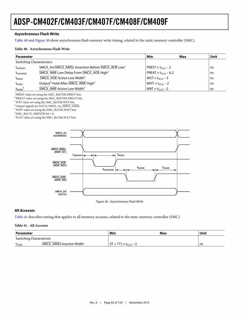
Rev. A | Page 82 of 124 | November 2015
ADSP-CM402F/CM403F/CM407F/CM408F/CM409FAsynchronous Flash Write
Table 40 and Figure 30 show asynchronous flash memory write timing, related to the static memory controller (SMC).
All Accesses
Table 41 describes timing that applies to all memory accesses, related to the static memory controller (SMC).
Table 40. Asynchronous Flash Write
Parameter Min Max UnitSwitching CharacteristicstAMSADV SMC0_Ax/SMC0_AMSx Assertion Before SMC0_AOE Low1
1 PREST value set using the SMC_BxETIM.PREST bits.
PREST × tSCLK – 2 nstDADVAWE SMC0_AWE Low Delay From SMC0_AOE High2
2 PREAT value set using the SMC_BxETIM.PREAT bits.
PREAT × tSCLK – 6.2 nstWADV SMC0_AOE Active Low Width3
3 WST value set using the SMC_BxTIM.WST bits.
WST × tSCLK – 3 ns tHAWE Output4 Hold After SMC0_AWE High5
4 Output signals are DATA, SMC0_Ax, SMC0_AMSx.5 WHT value set using the SMC_BxTIM.WHT bits.
WHT × tSCLK – 2 nstWAWE
6
6 SMC_BxCTL.ARDYEN bit = 0.
SMC0_AWE Active Low Width7
7 WAT value set using the SMC_BxTIM.WAT bits.
WAT × tSCLK – 2 ns
Figure 30. Asynchronous Flash Write
Table 41. All Accesses
Parameter Min Max UnitSwitching CharacteristictTURN SMC0_AMSx Inactive Width (IT + TT) × tSCLK – 2 ns
SMC0_AMSx (NOR_CE )
SMC0_AWE (NOR_WE)
SMC0_Ax(ADDRESS)
SMC0_AOE (NOR_ADV)
tAMSADV
tDADVAWE
SMC0_DX(DATA)
tWADV
tWAWE tHAWE
Rev. A | Page 83 of 124 | November 2015
ADSP-CM402F/CM403F/CM407F/CM408F/CM409FSerial Ports
To determine whether serial port (SPORT) communication is possible between two devices at clock speed n, the following specifications must be confirmed: 1) frame sync delay and frame sync setup and hold, 2) data delay and data setup and hold, and 3) serial clock (SPT_CLK) width. In Figure 31 either the rising edge or the falling edge of SPT_CLK (external or internal) can be used as the active sampling edge. When externally generated the SPORT clock is called fSPTCLKEXT:
When internally generated, the programmed SPORT clock (fSPTCLKPROG) frequency in MHz is set by the following equation where CLKDIV is a field in the SPORT_DIV register that can be set from 0 to 65,535:
Table 42. Serial Ports—External Clock
Parameter Min Max UnitTiming RequirementstSFSE Frame Sync Setup Before SPT_CLK
(Externally Generated Frame Sync in either Transmit or Receive Mode)1
1 Referenced to sample edge.
2 ns
tHFSE Frame Sync Hold After SPT_CLK (Externally Generated Frame Sync in either Transmit or Receive Mode)1
2.7 ns
tSDRE Receive Data Setup Before Receive SPT_CLK1 2 ns tHDRE Receive Data Hold After SPT_CLK1 2.7 ns tSCLKW SPT_CLK Width2
2 This specification indicates the minimum instantaneous width or period that can be tolerated due to duty cycle variation or jitter on the external SPT_CLK. For the external SPT_CLK maximum frequency, see the fSPTCLKEXT specification in Table 27 Clock Related Operating Conditions.
0.5 × tSPTCLKEXT – 1 ns tSPTCLK SPT_CLK Period2 tSPTCLKEXT – 1 nsSwitching CharacteristicstDFSE Frame Sync Delay After SPT_CLK
(Internally Generated Frame Sync in either Transmit or Receive Mode)3
3 Referenced to drive edge.
14.5 ns
tHOFSE Frame Sync Hold After SPT_CLK (Internally Generated Frame Sync in either Transmit or Receive Mode)3
2 ns
tDDTE Transmit Data Delay After Transmit SPT_CLK3 14 ns tHDTE Transmit Data Hold After Transmit SPT_CLK3 2 ns
tSPTCLKEXT1
fSPTCLKEXT-------------------------------=
fSPTCLKPROGfSCLK
CLKDIV 1+ -------------------------------------=
tSPTCLKPROG1
fSPTCLKPROG-----------------------------------=
Rev. A | Page 84 of 124 | November 2015
ADSP-CM402F/CM403F/CM407F/CM408F/CM409FTable 43. Serial Ports—Internal Clock
Parameter Min Max UnitTiming RequirementstSFSI Frame Sync Setup Before SPT_CLK
(Externally Generated Frame Sync in either Transmit or Receive Mode)1
12 ns
tHFSI Frame Sync Hold After SPT_CLK(Externally Generated Frame Sync in either Transmit or Receive Mode)1
–0.5 ns
tSDRI Receive Data Setup Before SPT_CLK1 3.4 ns tHDRI Receive Data Hold After SPT_CLK1 1.5 ns Switching CharacteristicstDFSI Frame Sync Delay After SPT_CLK (Internally Generated
Frame Sync in Transmit or Receive Mode)23.5 ns
tHOFSI Frame Sync Hold After SPT_CLK (Internally Generated Frame Sync in Transmit or Receive Mode)2
–1 ns
tDDTI Transmit Data Delay After SPT_CLK2 3.5 ns tHDTI Transmit Data Hold After SPT_CLK2 –1.25 ns tSCLKIW SPT_CLK Width3 0.5 × tSPTCLKPROG – 1 nstSPTCLK SPT_CLK Period3 tSPTCLKPROG – 1 ns
1 Referenced to the sample edge.2 Referenced to drive edge.3 See Table 27 Clock Related Operating Conditions for details on the minimum period that may be programmed for fSPTCLKPROG.
Rev. A | Page 85 of 124 | November 2015
ADSP-CM402F/CM403F/CM407F/CM408F/CM409F
Figure 31. Serial Ports
DRIVE EDGE SAMPLE EDGE
SPT_A/BDx(DATA CHANNEL A/B)
SPT_A/BFS(FRAME SYNC)
SPT_A/BCLK(SPORT CLOCK)
tHOFSI tHFSI
tHDRI
DATA RECEIVE—INTERNAL CLOCK
DRIVE EDGE SAMPLE EDGE
tHFSI
tDDTI
DATA TRANSMIT—INTERNAL CLOCK
DRIVE EDGE SAMPLE EDGE
tHOFSEtHOFSI
tHDTI
tHFSE
tHDTE
tDDTE
DATA TRANSMIT—EXTERNAL CLOCK
DRIVE EDGE SAMPLE EDGE
tHOFSE tHFSE
tHDRE
DATA RECEIVE—EXTERNAL CLOCK
tSCLKIW
tDFSI
tSFSI
tSDRI
tSCLKW
tDFSE
tSFSE
tSDRE
tDFSE
tSFSEtSFSI
tDFSI
tSCLKIW tSCLKW
SPT_A/BDx(DATA CHANNEL A/B)
SPT_A/BFS(FRAME SYNC)
SPT_A/BCLK(SPORT CLOCK)
SPT_A/BDx(DATA CHANNEL A/B)
SPT_A/BFS(FRAME SYNC)
SPT_A/BCLK(SPORT CLOCK)
SPT_A/BDx(DATA CHANNEL A/B)
SPT_A/BFS(FRAME SYNC)
SPT_A/BCLK(SPORT CLOCK)

Rev. A | Page 86 of 124 | November 2015
ADSP-CM402F/CM403F/CM407F/CM408F/CM409FTable 44. Serial Ports—Enable and Three-State
Parameter Min Max UnitSwitching CharacteristicstDDTEN Data Enable from External Transmit SPT_CLK1 1 ns tDDTTE Data Disable from External Transmit SPT_CLK1 14 ns tDDTIN Data Enable from Internal Transmit SPT_CLK1 –1 ns tDDTTI Data Disable from Internal Transmit SPT_CLK1 2.8 ns
1 Referenced to drive edge.
Figure 32. Serial Ports—Enable and Three-State
DRIVE EDGE DRIVE EDGE
tDDTIN
tDDTEN tDDTTE
SPT_CLK(SPORT CLOCK
INTERNAL)
SPT_A/BDx(DATA
CHANNEL A/B)
SPT_CLK(SPORT CLOCK
EXTERNAL)
SPT_A/BDx(DATA
CHANNEL A/B)
DRIVE EDGE DRIVE EDGE
tDDTTI
Rev. A | Page 87 of 124 | November 2015
ADSP-CM402F/CM403F/CM407F/CM408F/CM409FThe SPT_TDV output signal becomes active in SPORT multichannel mode. During transmit slots (enabled with active channel selection registers) the SPT_TDV is asserted for communication with external devices.
Table 45. Serial Ports—Transmit Data Valid (TDV)
Parameter Min Max UnitSwitching CharacteristicstDRDVEN Data-Valid Enable Delay from Drive Edge of External Clock1
1 Referenced to drive edge.
2 ns tDFDVEN Data-Valid Disable Delay from Drive Edge of External Clock1 14 ns tDRDVIN Data-Valid Enable Delay from Drive Edge of Internal Clock1 –1 ns tDFDVIN Data-Valid Disable Delay from Drive Edge of Internal Clock1 3.5 ns
Figure 33. Serial Ports—Transmit Data Valid Internal and External Clock
DRIVE EDGE DRIVE EDGE
SPT_CLK(SPORT CLOCK
EXTERNAL)
tDRDVEN tDFDVEN
DRIVE EDGE DRIVE EDGE
SPT_CLK(SPORT CLOCK
INTERNAL)
tDRDVIN tDFDVIN
SPT_A/BTDV
SPT_A/BTDV
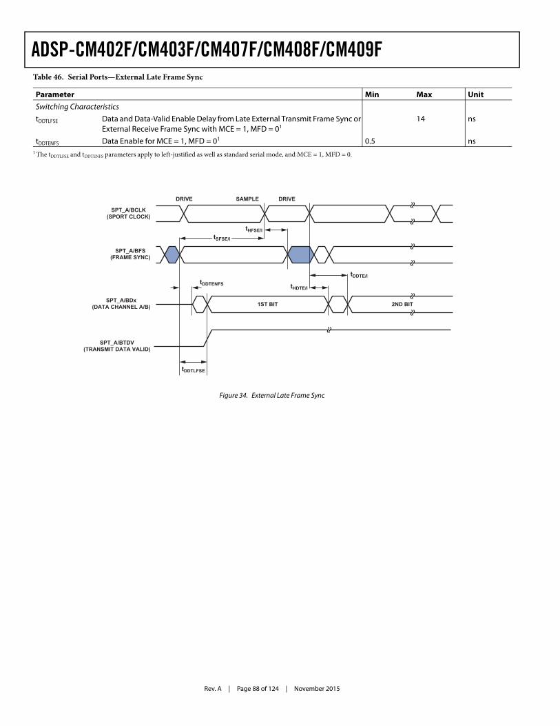
Rev. A | Page 88 of 124 | November 2015
ADSP-CM402F/CM403F/CM407F/CM408F/CM409FTable 46. Serial Ports—External Late Frame Sync
Parameter Min Max UnitSwitching CharacteristicstDDTLFSE Data and Data-Valid Enable Delay from Late External Transmit Frame Sync or
External Receive Frame Sync with MCE = 1, MFD = 01 14 ns
tDDTENFS Data Enable for MCE = 1, MFD = 01 0.5 ns1 The tDDTLFSE and tDDTENFS parameters apply to left-justified as well as standard serial mode, and MCE = 1, MFD = 0.
Figure 34. External Late Frame Sync
DRIVE SAMPLE
2ND BIT1ST BIT
DRIVE
tDDTE/I
tHDTE/I
tDDTLFSE
tDDTENFS
tSFSE/I
tHFSE/I
SPT_A/BDx(DATA CHANNEL A/B)
SPT_A/BFS(FRAME SYNC)
SPT_A/BCLK(SPORT CLOCK)
SPT_A/BTDV(TRANSMIT DATA VALID)
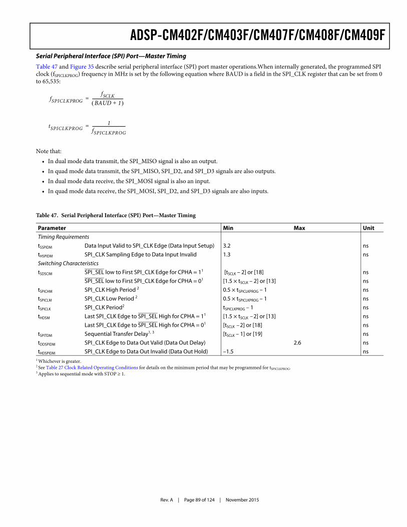
Rev. A | Page 89 of 124 | November 2015
ADSP-CM402F/CM403F/CM407F/CM408F/CM409FSerial Peripheral Interface (SPI) Port—Master Timing
Table 47 and Figure 35 describe serial peripheral interface (SPI) port master operations.When internally generated, the programmed SPI clock (fSPICLKPROG) frequency in MHz is set by the following equation where BAUD is a field in the SPI_CLK register that can be set from 0 to 65,535:
Note that: • In dual mode data transmit, the SPI_MISO signal is also an output.• In quad mode data transmit, the SPI_MISO, SPI_D2, and SPI_D3 signals are also outputs. • In dual mode data receive, the SPI_MOSI signal is also an input. • In quad mode data receive, the SPI_MOSI, SPI_D2, and SPI_D3 signals are also inputs.
Table 47. Serial Peripheral Interface (SPI) Port—Master Timing
Parameter Min Max UnitTiming RequirementstSSPIDM Data Input Valid to SPI_CLK Edge (Data Input Setup) 3.2 nstHSPIDM SPI_CLK Sampling Edge to Data Input Invalid 1.3 nsSwitching CharacteristicstSDSCIM SPI_SEL low to First SPI_CLK Edge for CPHA = 11
1 Whichever is greater.
[tSCLK – 2] or [18] nsSPI_SEL low to First SPI_CLK Edge for CPHA = 01 [1.5 × tSCLK – 2] or [13] ns
tSPICHM SPI_CLK High Period 2
2 See Table 27 Clock Related Operating Conditions for details on the minimum period that may be programmed for tSPICLKPROG.
0.5 × tSPICLKPROG – 1 nstSPICLM SPI_CLK Low Period 2 0.5 × tSPICLKPROG – 1 nstSPICLK SPI_CLK Period2 tSPICLKPROG – 1 nstHDSM Last SPI_CLK Edge to SPI_SEL High for CPHA = 11 [1.5 × tSCLK –2] or [13] ns
Last SPI_CLK Edge to SPI_SEL High for CPHA = 01 [tSCLK –2] or [18] nstSPITDM Sequential Transfer Delay1, 3
3 Applies to sequential mode with STOP ≥ 1.
[tSCLK – 1] or [19] nstDDSPIDM SPI_CLK Edge to Data Out Valid (Data Out Delay) 2.6 nstHDSPIDM SPI_CLK Edge to Data Out Invalid (Data Out Hold) –1.5 ns
fSPICLKPROGfSCLK
BAUD 1+ -------------------------------=
tSPICLKPROG1
fSPICLKPROG---------------------------------=
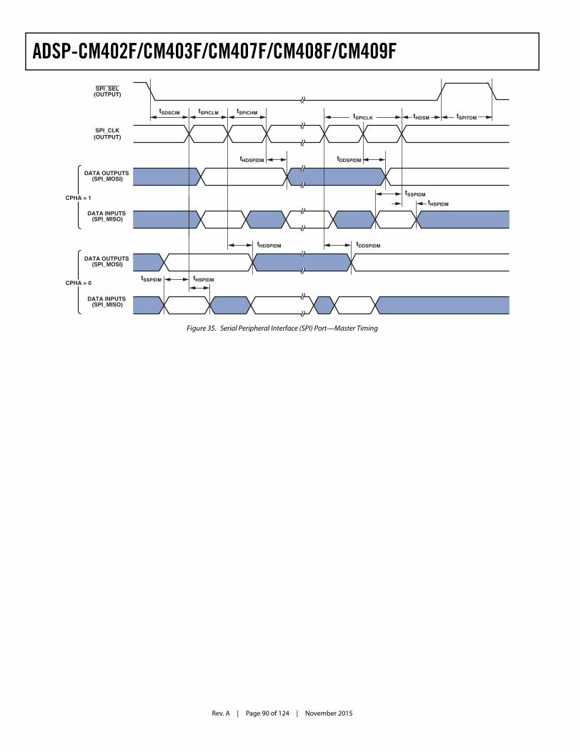
Rev. A | Page 90 of 124 | November 2015
ADSP-CM402F/CM403F/CM407F/CM408F/CM409F
Figure 35. Serial Peripheral Interface (SPI) Port—Master Timing
tSDSCIM tSPICLK tHDSM tSPITDMtSPICLM tSPICHM
tHDSPIDM
tHSPIDMtSSPIDM
SPI_SEL(OUTPUT)
SPI_CLK(OUTPUT)
DATA OUTPUTS (SPI_MOSI)
CPHA = 1
CPHA = 0
tDDSPIDM
tHSPIDM
tSSPIDM
tHDSPIDM
tDDSPIDM
DATA INPUTS (SPI_MISO)
DATA OUTPUTS (SPI_MOSI)
DATA INPUTS (SPI_MISO)
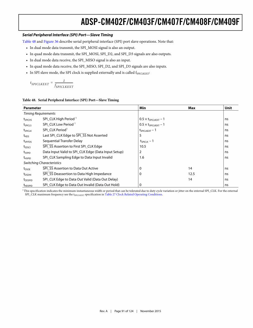
Rev. A | Page 91 of 124 | November 2015
ADSP-CM402F/CM403F/CM407F/CM408F/CM409FSerial Peripheral Interface (SPI) Port—Slave Timing
Table 48 and Figure 36 describe serial peripheral interface (SPI) port slave operations. Note that: • In dual mode data transmit, the SPI_MOSI signal is also an output.• In quad mode data transmit, the SPI_MOSI, SPI_D2, and SPI_D3 signals are also outputs. • In dual mode data receive, the SPI_MISO signal is also an input. • In quad mode data receive, the SPI_MISO, SPI_D2, and SPI_D3 signals are also inputs. • In SPI slave mode, the SPI clock is supplied externally and is called fSPICLKEXT:
Table 48. Serial Peripheral Interface (SPI) Port—Slave Timing
Parameter Min Max UnitTiming RequirementstSPICHS SPI_CLK High Period 1
1 This specification indicates the minimum instantaneous width or period that can be tolerated due to duty cycle variation or jitter on the external SPI_CLK. For the external SPI_CLK maximum frequency see the tSPICLKEXT specification in Table 27 Clock Related Operating Conditions.
0.5 × tSPICLKEXT – 1 nstSPICLS SPI_CLK Low Period 1 0.5 × tSPICLKEXT – 1 nstSPICLK SPI_CLK Period1 tSPICLKEXT – 1 nstHDS Last SPI_CLK Edge to SPI_SS Not Asserted 5 nstSPITDS Sequential Transfer Delay tSPICLK – 1 nstSDSCI SPI_SS Assertion to First SPI_CLK Edge 10.5 nstSSPID Data Input Valid to SPI_CLK Edge (Data Input Setup) 2 nstHSPID SPI_CLK Sampling Edge to Data Input Invalid 1.6 nsSwitching CharacteristicstDSOE SPI_SS Assertion to Data Out Active 0 14 nstDSDHI SPI_SS Deassertion to Data High Impedance 0 12.5 nstDDSPID SPI_CLK Edge to Data Out Valid (Data Out Delay) 14 nstHDSPID SPI_CLK Edge to Data Out Invalid (Data Out Hold) 0 ns
tSPICLKEXT1
fSPICLKEXT-----------------------------=
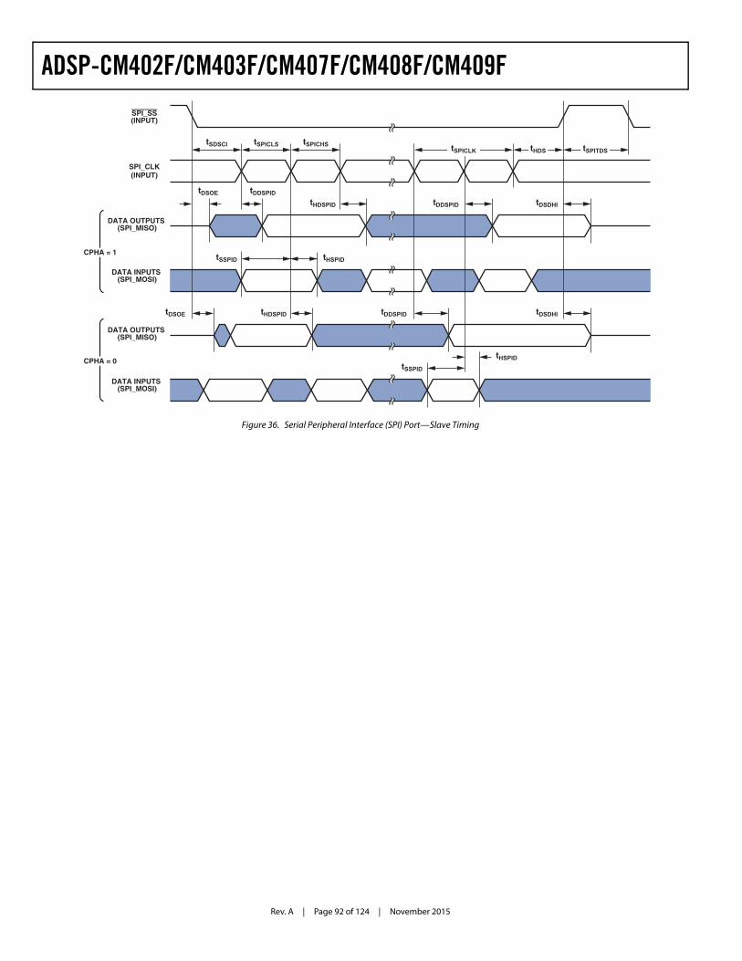
Rev. A | Page 92 of 124 | November 2015
ADSP-CM402F/CM403F/CM407F/CM408F/CM409F
Figure 36. Serial Peripheral Interface (SPI) Port—Slave Timing
tSPICLK tHDS tSPITDStSDSCI tSPICLS tSPICHS
tDSOE tDDSPIDtDDSPID tDSDHItHDSPID
tSSPID
tDSDHItHDSPIDtDSOE
tHSPIDtSSPID
tDDSPID
SPI_SS(INPUT)
SPI_CLK(INPUT)
tHSPID
DATA OUTPUTS (SPI_MISO)
CPHA = 1
CPHA = 0
DATA INPUTS (SPI_MOSI)
DATA OUTPUTS (SPI_MISO)
DATA INPUTS (SPI_MOSI)
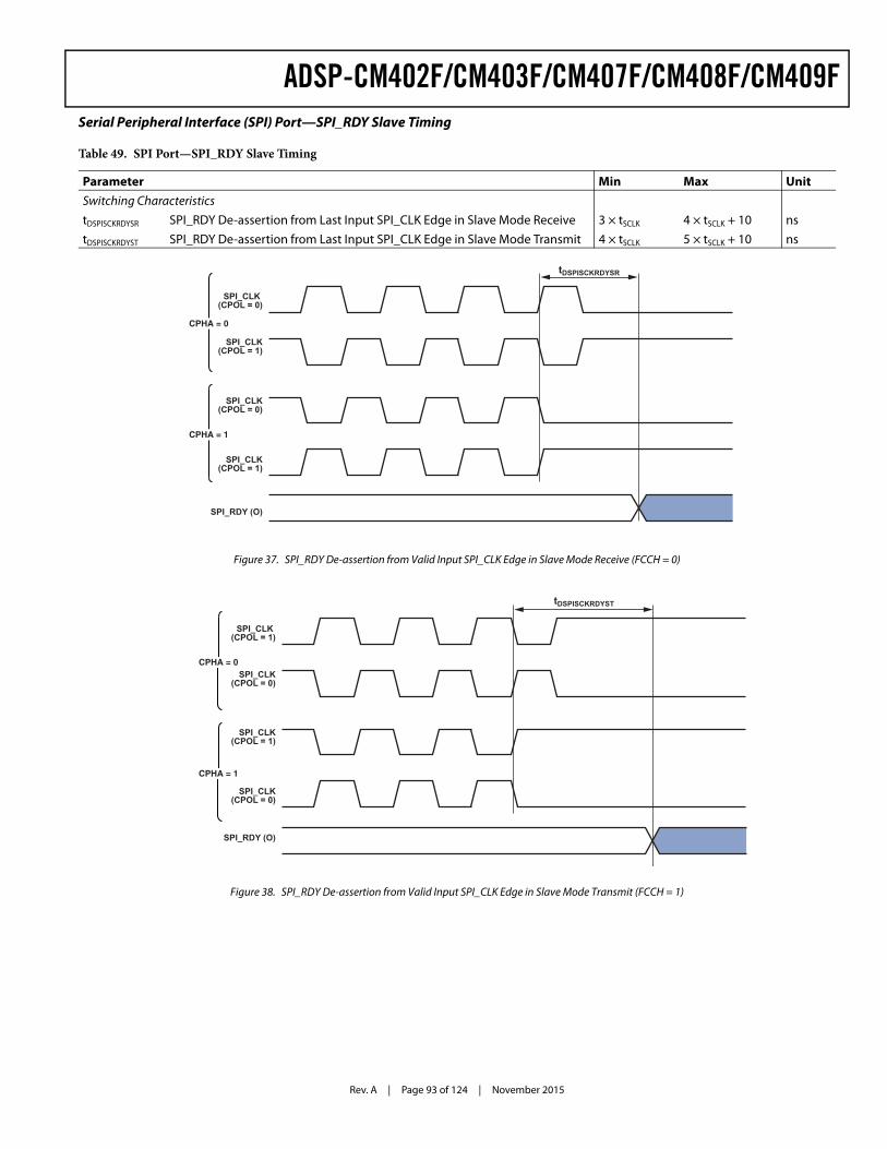
Rev. A | Page 93 of 124 | November 2015
ADSP-CM402F/CM403F/CM407F/CM408F/CM409FSerial Peripheral Interface (SPI) Port—SPI_RDY Slave Timing
Table 49. SPI Port—SPI_RDY Slave Timing
Parameter Min Max UnitSwitching CharacteristicstDSPISCKRDYSR SPI_RDY De-assertion from Last Input SPI_CLK Edge in Slave Mode Receive 3 × tSCLK 4 × tSCLK + 10 nstDSPISCKRDYST SPI_RDY De-assertion from Last Input SPI_CLK Edge in Slave Mode Transmit 4 × tSCLK 5 × tSCLK + 10 ns
Figure 37. SPI_RDY De-assertion from Valid Input SPI_CLK Edge in Slave Mode Receive (FCCH = 0)
Figure 38. SPI_RDY De-assertion from Valid Input SPI_CLK Edge in Slave Mode Transmit (FCCH = 1)
SPI_CLK (CPOL = 0)
SPI_CLK(CPOL = 1)
tDSPISCKRDYSR
SPI_RDY (O)
SPI_CLK(CPOL = 0)
SPI_CLK(CPOL = 1)
CPHA = 1
CPHA = 0
SPI_CLK (CPOL = 1)
SPI_CLK(CPOL = 0)
tDSPISCKRDYST
SPI_RDY (O)
SPI_CLK(CPOL = 1)
SPI_CLK(CPOL = 0)
CPHA = 1
CPHA = 0
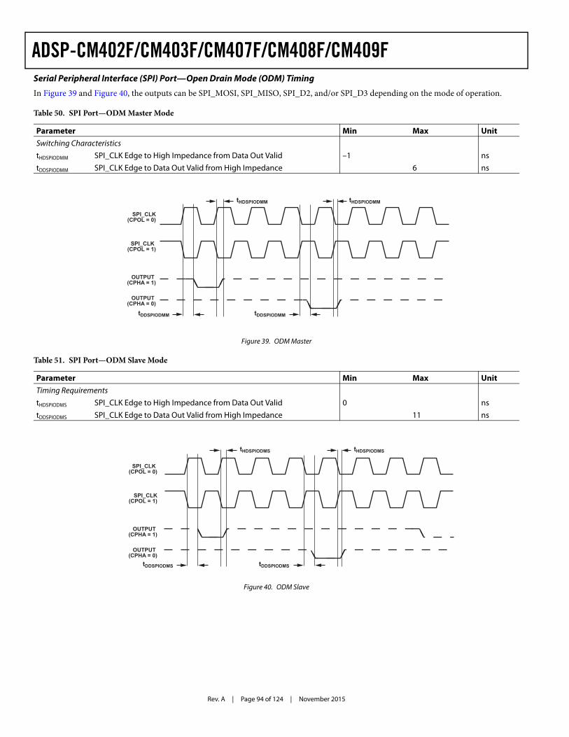
Rev. A | Page 94 of 124 | November 2015
ADSP-CM402F/CM403F/CM407F/CM408F/CM409FSerial Peripheral Interface (SPI) Port—Open Drain Mode (ODM) Timing
In Figure 39 and Figure 40, the outputs can be SPI_MOSI, SPI_MISO, SPI_D2, and/or SPI_D3 depending on the mode of operation.
Table 50. SPI Port—ODM Master Mode
Parameter Min Max UnitSwitching CharacteristicstHDSPIODMM SPI_CLK Edge to High Impedance from Data Out Valid –1 nstDDSPIODMM SPI_CLK Edge to Data Out Valid from High Impedance 6 ns
Figure 39. ODM Master
Table 51. SPI Port—ODM Slave Mode
Parameter Min Max UnitTiming RequirementstHDSPIODMS SPI_CLK Edge to High Impedance from Data Out Valid 0 nstDDSPIODMS SPI_CLK Edge to Data Out Valid from High Impedance 11 ns
Figure 40. ODM Slave
SPI_CLK(CPOL = 0)
tHDSPIODMM
SPI_CLK (CPOL = 1)
tDDSPIODMM tDDSPIODMM
tHDSPIODMM
OUTPUT (CPHA = 1)
OUTPUT (CPHA = 0)
tHDSPIODMS
tDDSPIODMS tDDSPIODMS
tHDSPIODMS
SPI_CLK (CPOL = 0)
SPI_CLK(CPOL = 1)
OUTPUT (CPHA = 1)
OUTPUT (CPHA = 0)
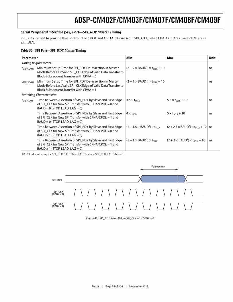
Rev. A | Page 95 of 124 | November 2015
ADSP-CM402F/CM403F/CM407F/CM408F/CM409FSerial Peripheral Interface (SPI) Port—SPI_RDY Master Timing
SPI_RDY is used to provide flow control. The CPOL and CPHA bits are set in SPI_CTL, while LEADX, LAGX, and STOP are in SPI_DLY.
Table 52. SPI Port—SPI_RDY Master Timing
Parameter Min Max UnitTiming RequirementstSRDYSCKM0 Minimum Setup Time for SPI_RDY De-assertion in Master
Mode Before Last Valid SPI_CLK Edge of Valid Data Transfer to Block Subsequent Transfer with CPHA = 0
(2 + 2 × BAUD1) × tSCLK + 10
1 BAUD value set using the SPI_CLK.BAUD bits. BAUD value = SPI_CLK.BAUD bits + 1.
ns
tSRDYSCKM1 Minimum Setup Time for SPI_RDY De-assertion in Master Mode Before Last Valid SPI_CLK Edge of Valid Data Transfer to Block Subsequent Transfer with CPHA = 1
(2 + 2 × BAUD1) × tSCLK + 10 ns
Switching CharacteristicstSRDYSCKM Time Between Assertion of SPI_RDY by Slave and First Edge
of SPI_CLK for New SPI Transfer with CPHA/CPOL = 0 and BAUD = 0 (STOP, LEAD, LAG = 0)
4.5 × tSCLK 5.5 × tSCLK + 10 ns
Time Between Assertion of SPI_RDY by Slave and First Edge of SPI_CLK for New SPI Transfer with CPHA/CPOL = 1 and BAUD = 0 (STOP, LEAD, LAG = 0)
4 × tSCLK 5 × tSCLK + 10 ns
Time Between Assertion of SPI_RDY by Slave and First Edge of SPI_CLK for New SPI Transfer with CPHA/CPOL = 0 and BAUD ≥ 1 (STOP, LEAD, LAG = 0)
(1 + 1.5 × BAUD1) × tSCLK (2 + 2.5 × BAUD1) × tSCLK + 10 ns
Time Between Assertion of SPI_RDY by Slave and First Edge of SPI_CLK for New SPI Transfer with CPHA/CPOL = 1 and BAUD ≥ 1 (STOP, LEAD, LAG = 0)
(1 + 1 × BAUD1) × tSCLK (2 + 2 × BAUD1) × tSCLK + 10 ns
Figure 41. SPI_RDY Setup Before SPI_CLK with CPHA = 0
SPI_CLK (CPOL = 0)
SPI_CLK (CPOL = 1)
tSRDYSCKM0
SPI_RDY
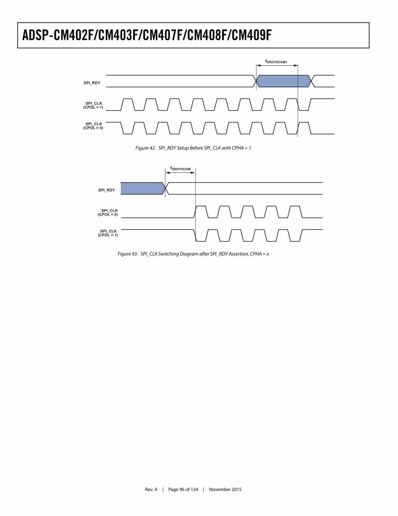
Rev. A | Page 96 of 124 | November 2015
ADSP-CM402F/CM403F/CM407F/CM408F/CM409F
Figure 42. SPI_RDY Setup Before SPI_CLK with CPHA = 1
Figure 43. SPI_CLK Switching Diagram after SPI_RDY Assertion, CPHA = x
SPI_CLK (CPOL = 1)
SPI_CLK (CPOL = 0)
tSRDYSCKM1
SPI_RDY
SPI_CLK(CPOL = 0)
SPI_CLK (CPOL = 1)
tSRDYSCKM
SPI_RDY
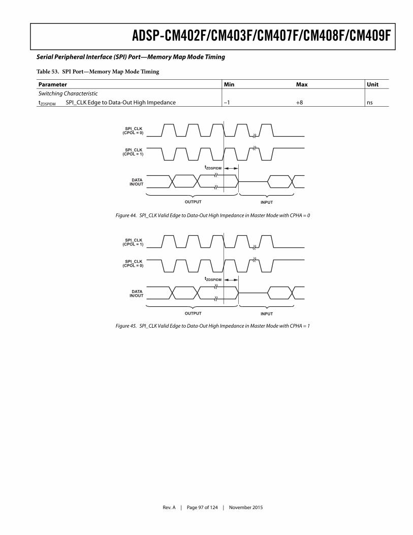
Rev. A | Page 97 of 124 | November 2015
ADSP-CM402F/CM403F/CM407F/CM408F/CM409FSerial Peripheral Interface (SPI) Port—Memory Map Mode Timing
Table 53. SPI Port—Memory Map Mode Timing
Parameter Min Max UnitSwitching CharacteristictZDSPIDM SPI_CLK Edge to Data-Out High Impedance –1 +8 ns
Figure 44. SPI_CLK Valid Edge to Data-Out High Impedance in Master Mode with CPHA = 0
Figure 45. SPI_CLK Valid Edge to Data-Out High Impedance in Master Mode with CPHA = 1
SPI_CLK (CPOL = 0)
SPI_CLK (CPOL = 1)
tZDSPIDM
DATA IN/OUT
OUTPUT INPUT
SPI_CLK (CPOL = 1)
SPI_CLK (CPOL = 0)
tZDSPIDM
DATA IN/OUT
OUTPUT INPUT
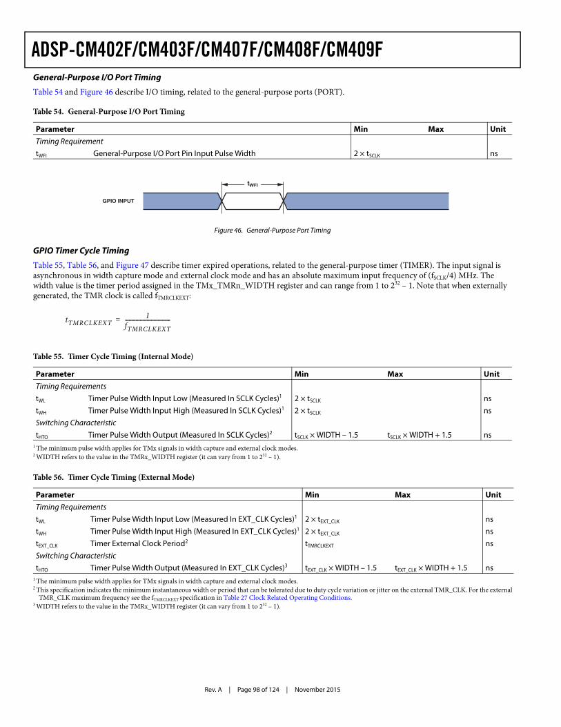
Rev. A | Page 98 of 124 | November 2015
ADSP-CM402F/CM403F/CM407F/CM408F/CM409FGeneral-Purpose I/O Port Timing
Table 54 and Figure 46 describe I/O timing, related to the general-purpose ports (PORT).
GPIO Timer Cycle Timing
Table 55, Table 56, and Figure 47 describe timer expired operations, related to the general-purpose timer (TIMER). The input signal is asynchronous in width capture mode and external clock mode and has an absolute maximum input frequency of (fSCLK/4) MHz. The width value is the timer period assigned in the TMx_TMRn_WIDTH register and can range from 1 to 232 – 1. Note that when externally generated, the TMR clock is called fTMRCLKEXT:
Table 54. General-Purpose I/O Port Timing
Parameter Min Max UnitTiming RequirementtWFI General-Purpose I/O Port Pin Input Pulse Width 2 × tSCLK ns
Figure 46. General-Purpose Port Timing
Table 55. Timer Cycle Timing (Internal Mode)
Parameter Min Max UnitTiming RequirementstWL Timer Pulse Width Input Low (Measured In SCLK Cycles)1
1 The minimum pulse width applies for TMx signals in width capture and external clock modes.
2 × tSCLK nstWH Timer Pulse Width Input High (Measured In SCLK Cycles)1 2 × tSCLK nsSwitching CharacteristictHTO Timer Pulse Width Output (Measured In SCLK Cycles)2
2 WIDTH refers to the value in the TMRx_WIDTH register (it can vary from 1 to 232 – 1).
tSCLK × WIDTH – 1.5 tSCLK × WIDTH + 1.5 ns
Table 56. Timer Cycle Timing (External Mode)
Parameter Min Max UnitTiming RequirementstWL Timer Pulse Width Input Low (Measured In EXT_CLK Cycles)1
1 The minimum pulse width applies for TMx signals in width capture and external clock modes.
2 × tEXT_CLK nstWH Timer Pulse Width Input High (Measured In EXT_CLK Cycles)1 2 × tEXT_CLK nstEXT_CLK Timer External Clock Period2
2 This specification indicates the minimum instantaneous width or period that can be tolerated due to duty cycle variation or jitter on the external TMR_CLK. For the external TMR_CLK maximum frequency see the fTMRCLKEXT specification in Table 27 Clock Related Operating Conditions.
tTMRCLKEXT nsSwitching CharacteristictHTO Timer Pulse Width Output (Measured In EXT_CLK Cycles)3
3 WIDTH refers to the value in the TMRx_WIDTH register (it can vary from 1 to 232 – 1).
tEXT_CLK × WIDTH – 1.5 tEXT_CLK × WIDTH + 1.5 ns
GPIO INPUT
tWFI
tTMRCLKEXT1
fTMRCLKEXT---------------------------------=
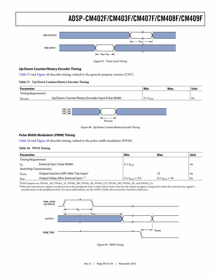
Rev. A | Page 99 of 124 | November 2015
ADSP-CM402F/CM403F/CM407F/CM408F/CM409F
Up/Down Counter/Rotary Encoder Timing
Table 57 and Figure 48 describe timing, related to the general-purpose counter (CNT).
Pulse Width Modulator (PWM) Timing
Table 58 and Figure 49 describe timing, related to the pulse width modulator (PWM).
Figure 47. Timer Cycle Timing
Table 57. Up/Down Counter/Rotary Encoder Timing
Parameter Min Max UnitTiming RequirementtWCOUNT Up/Down Counter/Rotary Encoder Input Pulse Width 2 × tSCLK ns
Figure 48. Up/Down Counter/Rotary Encoder Timing
Table 58. PWM Timing
Parameter Min Max UnitTiming RequirementtES External Sync Pulse Width 2 × tSCLK nsSwitching CharacteristicstDODIS Output Inactive (Off ) After Trip Input1
1 PWM outputs are: PWMx_AH, PWMx_AL, PWMx_BH, PWMx_BL, PWMx_CH, PWMx_DH, PWMx_DL, and PWMx_CL.
15 nstDOE Output Delay After External Sync1, 2
2 When the external sync signal is synchronous to the peripheral clock, it takes fewer clock cycles for the output to appear compared to when the external sync signal is asynchronous to the peripheral clock. For more information, see the ADSP-CM40x Microcontroller Hardware Reference.
2 × tSCLK + 5.5 5 × tSCLK + 14 ns
Figure 49. PWM Timing
TMR OUTPUT
TMR INPUT
tWH, tWL
tHTO
CNT_UDCNT_DGCNT_ZM
tWCOUNT
PWM_TRIP
PWM_SYNC(AS INPUT)
tES
tDOE
OUTPUT
tDODIS
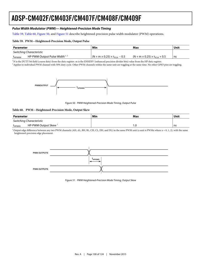
Rev. A | Page 100 of 124 | November 2015
ADSP-CM402F/CM403F/CM407F/CM408F/CM409FPulse Width Modulator (PWM)— Heightened-Precision Mode Timing
Table 59, Table 60, Figure 50, and Figure 51 describe heightened-precision pulse width modulator (PWM) operations.
Table 59. PWM—Heightened-Precision Mode, Output Pulse
Parameter Min Max UnitSwitching CharacteristictHPWMW HP-PWM Output Pulse Width1, 2
1 N is the DUTY bit field (coarse duty) from the duty register. m is the ENHDIV (enhanced precision divider bits) value from the HP duty register.2 Applies to individual PWM channel with 50% duty cycle. Other PWM channels within the same unit are toggling at the same time. No other GPIO pins are toggling.
(N + m × 0.25) × tSCLK – 0.5 (N + m × 0.25) × tSCLK + 0.5 ns
Figure 50. PWM Heightened-Precision Mode Timing, Output Pulse
Table 60. PWM—Heightened-Precision Mode, Output Skew
Parameter Min Max UnitSwitching CharacteristictHPWMS HP-PWM Output Skew 1
1 Output edge difference between any two PWM channels (AH, AL, BH, BL, CH, CL, DH, and DL) in the same PWM unit (a unit is PWMx where x = 0, 1, 2), with the same heightened-precision edge placement.
1.0 ns
Figure 51. PWM Heightened-Precision Mode Timing, Output Skew
PWMOUTPUTtHPWMW
PWM OUTPUTS
PWM OUTPUTS
tHPWMS
Rev. A | Page 101 of 124 | November 2015
ADSP-CM402F/CM403F/CM407F/CM408F/CM409FUniversal Asynchronous Receiver-Transmitter (UART) Ports—Receive and Transmit Timing
The universal asynchronous receiver-transmitter (UART) ports receive and transmit operations are described in the ADSP-CM40x Mixed-Signal Control Processor with ARM Cortex-M4 Hardware Reference.
Controller Area Network (CAN) Interface
The controller area network (CAN) interface timing is described in the ADSP-CM40x Mixed-Signal Control Processor with ARM Cortex-M4 Hardware Reference.
Universal Serial Bus (USB) On-The-Go—Receive and Transmit Timing
The universal serial bus (USB) on-the-go receive and transmit operations are described in the ADSP-CM40x Mixed-Signal Control Processor with ARM Cortex-M4 Hardware Reference.
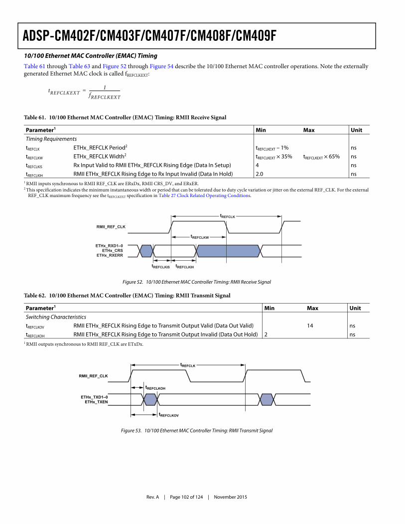
Rev. A | Page 102 of 124 | November 2015
ADSP-CM402F/CM403F/CM407F/CM408F/CM409F10/100 Ethernet MAC Controller (EMAC) Timing
Table 61 through Table 63 and Figure 52 through Figure 54 describe the 10/100 Ethernet MAC controller operations. Note the externally generated Ethernet MAC clock is called fREFCLKEXT:
Table 61. 10/100 Ethernet MAC Controller (EMAC) Timing: RMII Receive Signal
Parameter1
1 RMII inputs synchronous to RMII REF_CLK are ERxDx, RMII CRS_DV, and ERxER.
Min Max UnitTiming RequirementstREFCLK ETHx_REFCLK Period2
2 This specification indicates the minimum instantaneous width or period that can be tolerated due to duty cycle variation or jitter on the external REF_CLK. For the external REF_CLK maximum frequency see the tREFCLKEXT specification in Table 27 Clock Related Operating Conditions.
tREFCLKEXT – 1% nstREFCLKW ETHx_REFCLK Width2 tREFCLKEXT × 35% tREFCLKEXT × 65% nstREFCLKIS Rx Input Valid to RMII ETHx_REFCLK Rising Edge (Data In Setup) 4 nstREFCLKIH RMII ETHx_REFCLK Rising Edge to Rx Input Invalid (Data In Hold) 2.0 ns
Figure 52. 10/100 Ethernet MAC Controller Timing: RMII Receive Signal
Table 62. 10/100 Ethernet MAC Controller (EMAC) Timing: RMII Transmit Signal
Parameter1
1 RMII outputs synchronous to RMII REF_CLK are ETxDx.
Min Max UnitSwitching CharacteristicstREFCLKOV RMII ETHx_REFCLK Rising Edge to Transmit Output Valid (Data Out Valid) 14 nstREFCLKOH RMII ETHx_REFCLK Rising Edge to Transmit Output Invalid (Data Out Hold) 2 ns
Figure 53. 10/100 Ethernet MAC Controller Timing: RMII Transmit Signal
tREFCLKEXT1
fREFCLKEXT-------------------------------=
tREFCLKIS tREFCLKIH
ETHx_RXD1–0ETHx_CRS
ETHx_RXERR
RMII_REF_CLK
tREFCLKW
tREFCLK
tREFCLKOV
tREFCLKOH
RMII_REF_CLK
ETHx_TXD1–0ETHx_TXEN
tREFCLK
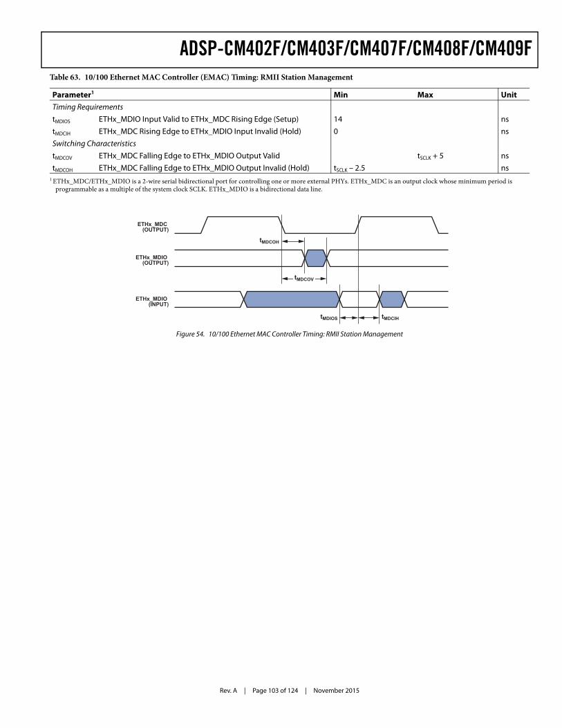
Rev. A | Page 103 of 124 | November 2015
ADSP-CM402F/CM403F/CM407F/CM408F/CM409FTable 63. 10/100 Ethernet MAC Controller (EMAC) Timing: RMII Station Management
Parameter1 Min Max UnitTiming RequirementstMDIOS ETHx_MDIO Input Valid to ETHx_MDC Rising Edge (Setup) 14 nstMDCIH ETHx_MDC Rising Edge to ETHx_MDIO Input Invalid (Hold) 0 nsSwitching CharacteristicstMDCOV ETHx_MDC Falling Edge to ETHx_MDIO Output Valid tSCLK + 5 nstMDCOH ETHx_MDC Falling Edge to ETHx_MDIO Output Invalid (Hold) tSCLK – 2.5 ns
1 ETHx_MDC/ETHx_MDIO is a 2-wire serial bidirectional port for controlling one or more external PHYs. ETHx_MDC is an output clock whose minimum period is programmable as a multiple of the system clock SCLK. ETHx_MDIO is a bidirectional data line.
Figure 54. 10/100 Ethernet MAC Controller Timing: RMII Station Management
ETHx_MDIO (INPUT)
ETHx_MDIO (OUTPUT)
ETHx_MDC (OUTPUT)
tMDIOS
tMDCOH
tMDCIH
tMDCOV
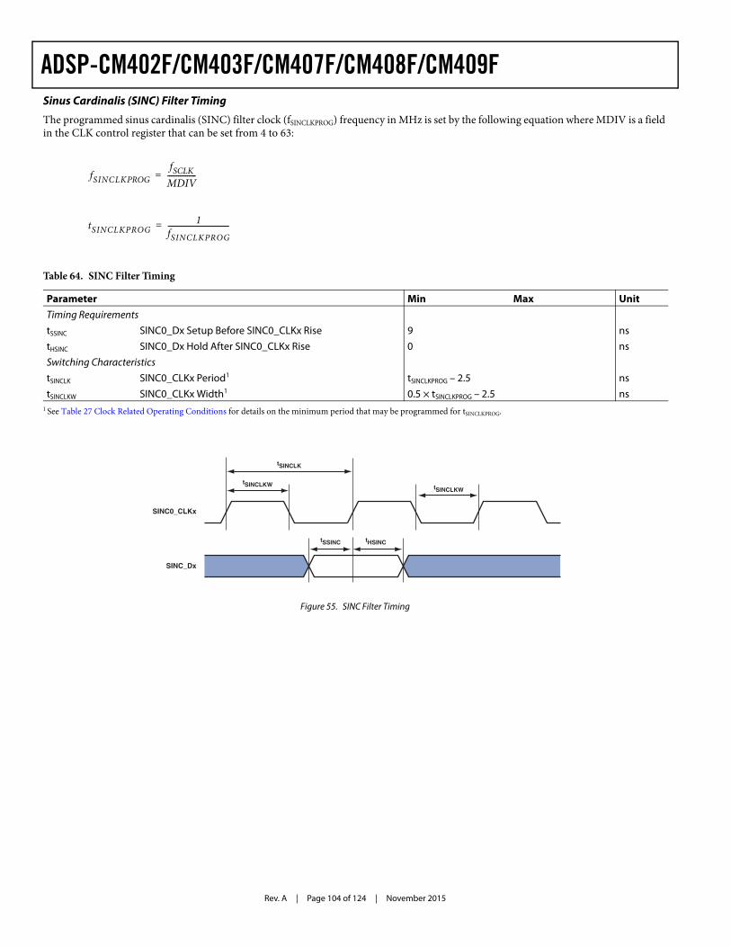
Rev. A | Page 104 of 124 | November 2015
ADSP-CM402F/CM403F/CM407F/CM408F/CM409FSinus Cardinalis (SINC) Filter Timing
The programmed sinus cardinalis (SINC) filter clock (fSINCLKPROG) frequency in MHz is set by the following equation where MDIV is a field in the CLK control register that can be set from 4 to 63:
Table 64. SINC Filter Timing
Parameter Min Max UnitTiming RequirementstSSINC SINC0_Dx Setup Before SINC0_CLKx Rise 9 nstHSINC SINC0_Dx Hold After SINC0_CLKx Rise 0 nsSwitching CharacteristicstSINCLK SINC0_CLKx Period1
1 See Table 27 Clock Related Operating Conditions for details on the minimum period that may be programmed for tSINCLKPROG.
tSINCLKPROG – 2.5 nstSINCLKW SINC0_CLKx Width1 0.5 × tSINCLKPROG – 2.5 ns
Figure 55. SINC Filter Timing
fSINCLKPROGfSCLK
MDIV----------------=
tSINCLKPROG1
fSINCLKPROG----------------------------------=
SINC0_CLKx
SINC_Dx
tSINCLK
tSINCLKWtSINCLKW
tSSINC tHSINC
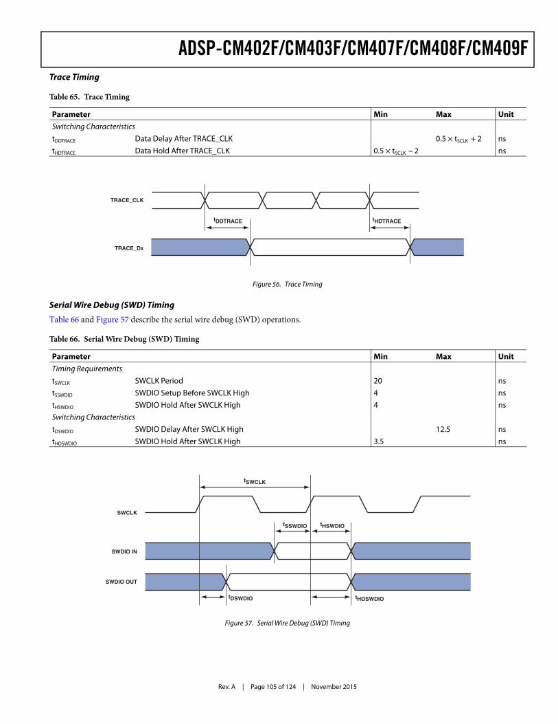
Rev. A | Page 105 of 124 | November 2015
ADSP-CM402F/CM403F/CM407F/CM408F/CM409FTrace Timing
Serial Wire Debug (SWD) Timing
Table 66 and Figure 57 describe the serial wire debug (SWD) operations.
Table 65. Trace Timing
Parameter Min Max UnitSwitching CharacteristicstDDTRACE Data Delay After TRACE_CLK 0.5 × tSCLK + 2 nstHDTRACE Data Hold After TRACE_CLK 0.5 × tSCLK – 2 ns
Figure 56. Trace Timing
Table 66. Serial Wire Debug (SWD) Timing
Parameter Min Max UnitTiming RequirementstSWCLK SWCLK Period 20 nstSSWDIO SWDIO Setup Before SWCLK High 4 nstHSWDIO SWDIO Hold After SWCLK High 4 nsSwitching CharacteristicstDSWDIO SWDIO Delay After SWCLK High 12.5 nstHOSWDIO SWDIO Hold After SWCLK High 3.5 ns
Figure 57. Serial Wire Debug (SWD) Timing
TRACE_CLK
TRACE_Dx
tDDTRACE tHDTRACE
SWCLK
SWDIO IN
tSWCLK
tSSWDIO tHSWDIO
tDSWDIO tHOSWDIO
SWDIO OUT
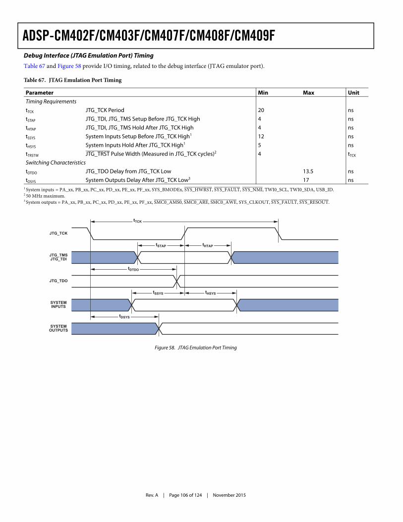
Rev. A | Page 106 of 124 | November 2015
ADSP-CM402F/CM403F/CM407F/CM408F/CM409FDebug Interface (JTAG Emulation Port) Timing
Table 67 and Figure 58 provide I/O timing, related to the debug interface (JTAG emulator port).
Table 67. JTAG Emulation Port Timing
Parameter Min Max UnitTiming RequirementstTCK JTG_TCK Period 20 nstSTAP JTG_TDI, JTG_TMS Setup Before JTG_TCK High 4 nstHTAP JTG_TDI, JTG_TMS Hold After JTG_TCK High 4 nstSSYS System Inputs Setup Before JTG_TCK High1
1 System inputs = PA_xx, PB_xx, PC_xx, PD_xx, PE_xx, PF_xx, SYS_BMODEx, SYS_HWRST, SYS_FAULT, SYS_NMI, TWI0_SCL, TWI0_SDA, USB_ID.
12 nstHSYS System Inputs Hold After JTG_TCK High1 5 nstTRSTW JTG_TRST Pulse Width (Measured in JTG_TCK cycles)2
2 50 MHz maximum.
4 tTCK
Switching CharacteristicstDTDO JTG_TDO Delay from JTG_TCK Low 13.5 nstDSYS System Outputs Delay After JTG_TCK Low3
3 System outputs = PA_xx, PB_xx, PC_xx, PD_xx, PE_xx, PF_xx, SMC0_AMS0, SMC0_ARE, SMC0_AWE, SYS_CLKOUT, SYS_FAULT, SYS_RESOUT.
17 ns
Figure 58. JTAG Emulation Port Timing
JTG_TCK
JTG_TMSJTG_TDI
JTG_TDO
SYSTEMINPUTS
SYSTEMOUTPUTS
tTCK
tSTAP tHTAP
tDTDO
tSSYS tHSYS
tDSYS
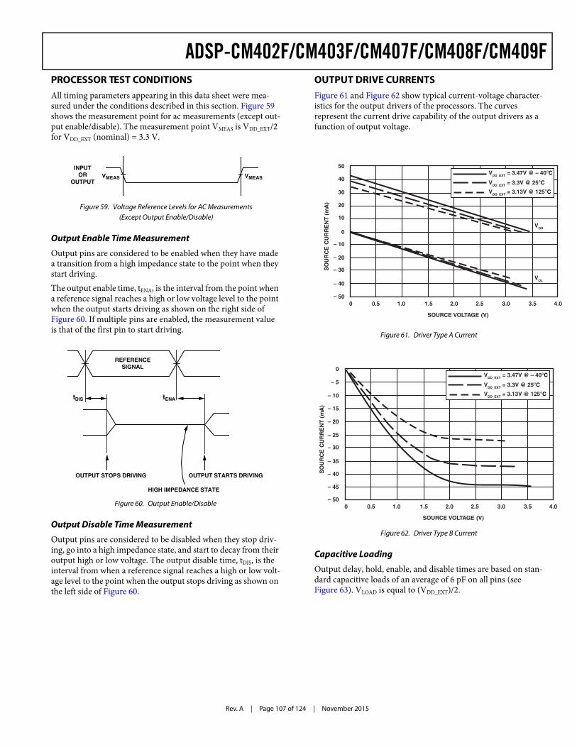
Rev. A | Page 107 of 124 | November 2015
ADSP-CM402F/CM403F/CM407F/CM408F/CM409FPROCESSOR TEST CONDITIONSAll timing parameters appearing in this data sheet were mea-sured under the conditions described in this section. Figure 59 shows the measurement point for ac measurements (except out-put enable/disable). The measurement point VMEAS is VDD_EXT/2 for VDD_EXT (nominal) = 3.3 V.
Output Enable Time Measurement
Output pins are considered to be enabled when they have made a transition from a high impedance state to the point when they start driving. The output enable time, tENA, is the interval from the point when a reference signal reaches a high or low voltage level to the point when the output starts driving as shown on the right side of Figure 60. If multiple pins are enabled, the measurement value is that of the first pin to start driving.
Output Disable Time Measurement
Output pins are considered to be disabled when they stop driv-ing, go into a high impedance state, and start to decay from their output high or low voltage. The output disable time, tDIS, is the interval from when a reference signal reaches a high or low volt-age level to the point when the output stops driving as shown on the left side of Figure 60.
OUTPUT DRIVE CURRENTSFigure 61 and Figure 62 show typical current-voltage character-istics for the output drivers of the processors. The curves represent the current drive capability of the output drivers as a function of output voltage.
Capacitive Loading
Output delay, hold, enable, and disable times are based on stan-dard capacitive loads of an average of 6 pF on all pins (see Figure 63). VLOAD is equal to (VDD_EXT)/2.
Figure 59. Voltage Reference Levels for AC Measurements (Except Output Enable/Disable)
Figure 60. Output Enable/Disable
INPUTOR
OUTPUTVMEAS VMEAS
REFERENCESIGNAL
tDIS
OUTPUT STARTS DRIVING
HIGH IMPEDANCE STATE
OUTPUT STOPS DRIVING
tENA
Figure 61. Driver Type A Current
Figure 62. Driver Type B Current
0
SO
UR
CE
CU
RR
EN
T (
mA
)
SOURCE VOLTAGE (V)
0 0.5 1.0 1.5 2.0 2.5 3.0 3.5
50
30
20
– 50
– 30
– 10
4.0
VDD_EXT = 3.47V @ – 40°C
VDD_EXT = 3.3V @ 25°C
– 20
– 40
10
40
VDD_EXT = 3.13V @ 125°C
VOH
VOL
– 25
SO
UR
CE
CU
RR
EN
T (
mA
)
SOURCE VOLTAGE (V)
0 0.5 1.0 1.5 2.0 2.5 3.0 3.5
0
– 5
– 10
– 50
– 30
4.0
VDD_EXT = 3.47V @ – 40°C
VDD_EXT = 3.3V @ 25°C
– 35
– 45
– 15
VDD_EXT = 3.13V @ 125°C
– 20
– 40
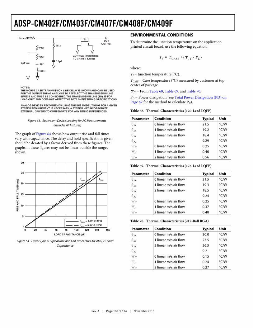
Rev. A | Page 108 of 124 | November 2015
ADSP-CM402F/CM403F/CM407F/CM408F/CM409F
The graph of Figure 64 shows how output rise and fall times vary with capacitance. The delay and hold specifications given should be derated by a factor derived from these figures. The graphs in these figures may not be linear outside the ranges shown.
ENVIRONMENTAL CONDITIONSTo determine the junction temperature on the application printed circuit board, use the following equation:
where:TJ = Junction temperature (°C).TCASE = Case temperature (°C) measured by customer at top center of package.JT = From Table 68, Table 69, and Table 70.PD = Power dissipation (see Total Power Dissipation (PD) on Page 67 for the method to calculate PD).
Figure 63. Equivalent Device Loading for AC Measurements (Includes All Fixtures)
Figure 64. Driver Type A Typical Rise and Fall Times (10% to 90%) vs. Load Capacitance
T1
ZO = 50Ω (impedance)TD = 4.04 ± 1.18 ns
2pF
50Ω
0.5pF
70Ω
400Ω
45Ω
4pF
NOTES:THE WORST CASE TRANSMISSION LINE DELAY IS SHOWN AND CAN BE USEDFOR THE OUTPUT TIMING ANALYSIS TO REFELECT THE TRANSMISSION LINEEFFECT AND MUST BE CONSIDERED. THE TRANSMISSION LINE (TD), IS FOR LOAD ONLY AND DOES NOT AFFECT THE DATA SHEET TIMING SPECIFICATIONS.
ANALOG DEVICES RECOMMENDS USING THE IBIS MODEL TIMING FOR A GIVEN SYSTEM REQUIREMENT. IF NECESSARY, A SYSTEM MAY INCORPORATE EXTERNAL DRIVERS TO COMPENSATE FOR ANY TIMING DIFFERENCES.
VLOADDUT
OUTPUT
LOAD CAPACITANCE (pF)
20
0
25
15
5
10
RIS
E A
ND
FA
LL
TIM
ES
(n
s)
0 16012020 60 100
30
tFALL = 3.3V @ 25°C
tRISE = 3.3V @ 25°C
40 80 140
tFALLtRISE
Table 68. Thermal Characteristics (120-Lead LQFP)
Parameter Condition Typical UnitJA 0 linear m/s air flow 21.5 °C/WJA 1 linear m/s air flow 19.2 °C/WJA 2 linear m/s air flow 18.4 °C/WJC 9.29 °C/WJT 0 linear m/s air flow 0.25 °C/WJT 1 linear m/s air flow 0.40 °C/WJT 2 linear m/s air flow 0.56 °C/W
Table 69. Thermal Characteristics (176-Lead LQFP)
Parameter Condition Typical UnitJA 0 linear m/s air flow 21.5 °C/WJA 1 linear m/s air flow 19.3 °C/WJA 2 linear m/s air flow 18.5 °C/WJC 9.24 °C/WJT 0 linear m/s air flow 0.25 °C/WJT 1 linear m/s air flow 0.37 °C/WJT 2 linear m/s air flow 0.48 °C/W
Table 70. Thermal Characteristics (212-Ball BGA)
Parameter Condition Typical UnitJA 0 linear m/s air flow 30.0 °C/WJA 1 linear m/s air flow 27.5 °C/WJA 2 linear m/s air flow 26.5 °C/WJC 9.2 °C/WJT 0 linear m/s air flow 0.15 °C/WJT 1 linear m/s air flow 0.24 °C/WJT 2 linear m/s air flow 0.27 °C/W
TJ TCASE JT PD +=
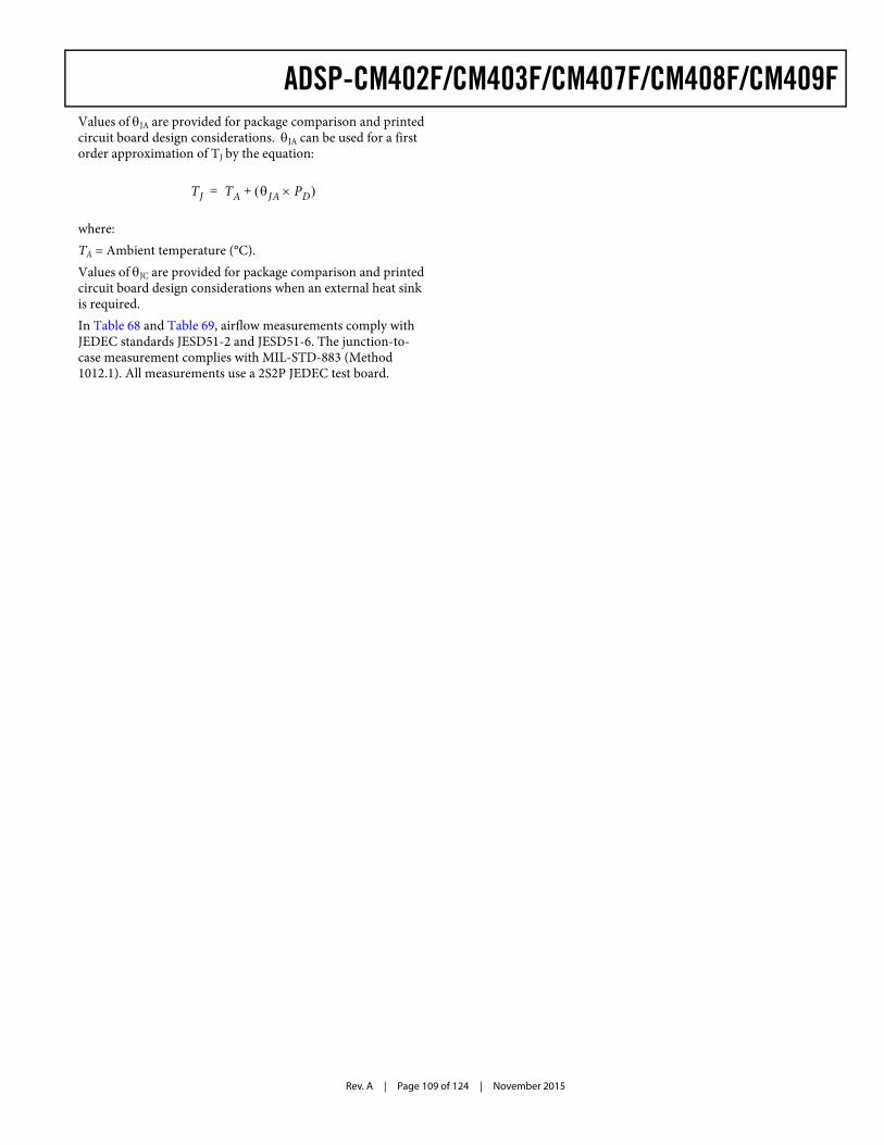
Rev. A | Page 109 of 124 | November 2015
ADSP-CM402F/CM403F/CM407F/CM408F/CM409FValues of JA are provided for package comparison and printed circuit board design considerations. JA can be used for a first order approximation of TJ by the equation:
where:TA = Ambient temperature (°C).Values of JC are provided for package comparison and printed circuit board design considerations when an external heat sink is required.In Table 68 and Table 69, airflow measurements comply with JEDEC standards JESD51-2 and JESD51-6. The junction-to-case measurement complies with MIL-STD-883 (Method 1012.1). All measurements use a 2S2P JEDEC test board.
TJ TA JA PD +=
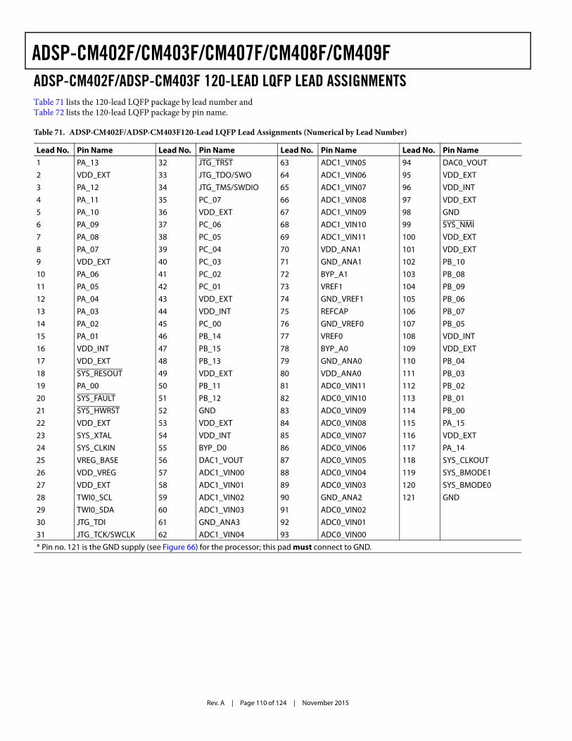
Rev. A | Page 110 of 124 | November 2015
ADSP-CM402F/CM403F/CM407F/CM408F/CM409FADSP-CM402F/ADSP-CM403F 120-LEAD LQFP LEAD ASSIGNMENTSTable 71 lists the 120-lead LQFP package by lead number and Table 72 lists the 120-lead LQFP package by pin name.
Table 71. ADSP-CM402F/ADSP-CM403F120-Lead LQFP Lead Assignments (Numerical by Lead Number)
Lead No. Pin Name Lead No. Pin Name Lead No. Pin Name Lead No. Pin Name1 PA_13 32 JTG_TRST 63 ADC1_VIN05 94 DAC0_VOUT2 VDD_EXT 33 JTG_TDO/SWO 64 ADC1_VIN06 95 VDD_EXT3 PA_12 34 JTG_TMS/SWDIO 65 ADC1_VIN07 96 VDD_INT4 PA_11 35 PC_07 66 ADC1_VIN08 97 VDD_EXT5 PA_10 36 VDD_EXT 67 ADC1_VIN09 98 GND6 PA_09 37 PC_06 68 ADC1_VIN10 99 SYS_NMI7 PA_08 38 PC_05 69 ADC1_VIN11 100 VDD_EXT8 PA_07 39 PC_04 70 VDD_ANA1 101 VDD_EXT9 VDD_EXT 40 PC_03 71 GND_ANA1 102 PB_1010 PA_06 41 PC_02 72 BYP_A1 103 PB_0811 PA_05 42 PC_01 73 VREF1 104 PB_0912 PA_04 43 VDD_EXT 74 GND_VREF1 105 PB_0613 PA_03 44 VDD_INT 75 REFCAP 106 PB_0714 PA_02 45 PC_00 76 GND_VREF0 107 PB_0515 PA_01 46 PB_14 77 VREF0 108 VDD_INT16 VDD_INT 47 PB_15 78 BYP_A0 109 VDD_EXT17 VDD_EXT 48 PB_13 79 GND_ANA0 110 PB_0418 SYS_RESOUT 49 VDD_EXT 80 VDD_ANA0 111 PB_0319 PA_00 50 PB_11 81 ADC0_VIN11 112 PB_0220 SYS_FAULT 51 PB_12 82 ADC0_VIN10 113 PB_0121 SYS_HWRST 52 GND 83 ADC0_VIN09 114 PB_0022 VDD_EXT 53 VDD_EXT 84 ADC0_VIN08 115 PA_1523 SYS_XTAL 54 VDD_INT 85 ADC0_VIN07 116 VDD_EXT24 SYS_CLKIN 55 BYP_D0 86 ADC0_VIN06 117 PA_1425 VREG_BASE 56 DAC1_VOUT 87 ADC0_VIN05 118 SYS_CLKOUT26 VDD_VREG 57 ADC1_VIN00 88 ADC0_VIN04 119 SYS_BMODE127 VDD_EXT 58 ADC1_VIN01 89 ADC0_VIN03 120 SYS_BMODE028 TWI0_SCL 59 ADC1_VIN02 90 GND_ANA2 121 GND29 TWI0_SDA 60 ADC1_VIN03 91 ADC0_VIN0230 JTG_TDI 61 GND_ANA3 92 ADC0_VIN0131 JTG_TCK/SWCLK 62 ADC1_VIN04 93 ADC0_VIN00* Pin no. 121 is the GND supply (see Figure 66) for the processor; this pad must connect to GND.
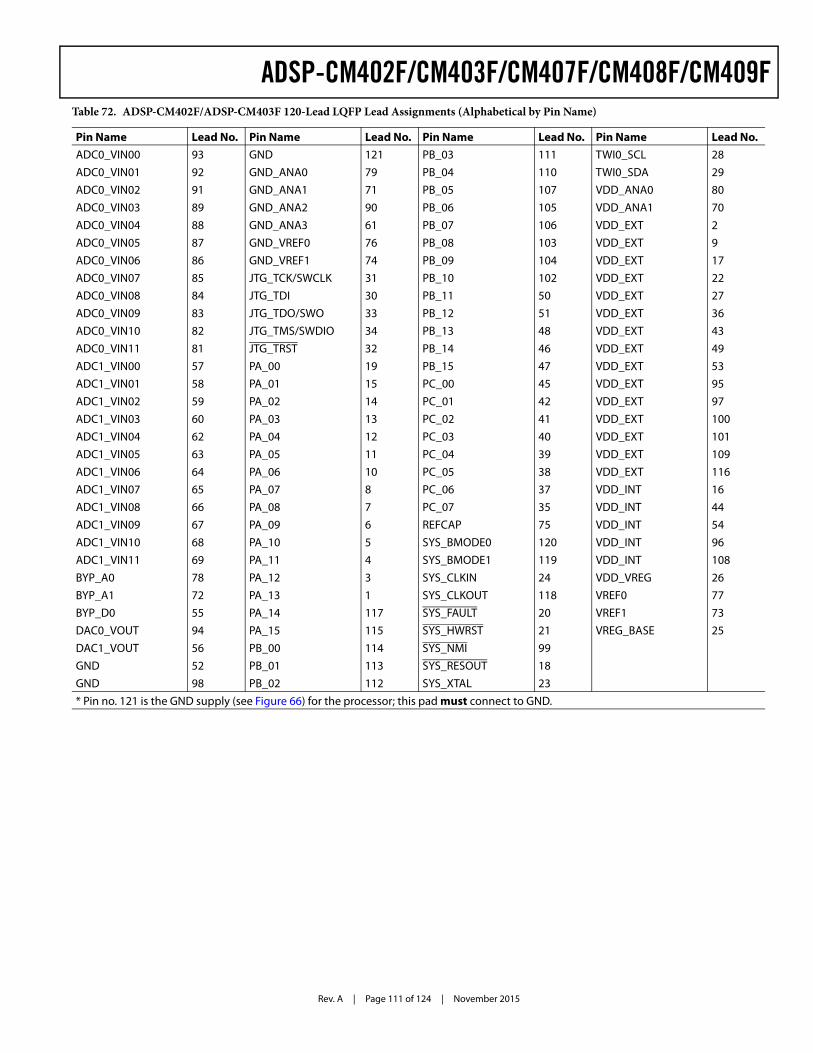
Rev. A | Page 111 of 124 | November 2015
ADSP-CM402F/CM403F/CM407F/CM408F/CM409FTable 72. ADSP-CM402F/ADSP-CM403F 120-Lead LQFP Lead Assignments (Alphabetical by Pin Name)
Pin Name Lead No. Pin Name Lead No. Pin Name Lead No. Pin Name Lead No.ADC0_VIN00 93 GND 121 PB_03 111 TWI0_SCL 28ADC0_VIN01 92 GND_ANA0 79 PB_04 110 TWI0_SDA 29ADC0_VIN02 91 GND_ANA1 71 PB_05 107 VDD_ANA0 80ADC0_VIN03 89 GND_ANA2 90 PB_06 105 VDD_ANA1 70ADC0_VIN04 88 GND_ANA3 61 PB_07 106 VDD_EXT 2ADC0_VIN05 87 GND_VREF0 76 PB_08 103 VDD_EXT 9ADC0_VIN06 86 GND_VREF1 74 PB_09 104 VDD_EXT 17ADC0_VIN07 85 JTG_TCK/SWCLK 31 PB_10 102 VDD_EXT 22ADC0_VIN08 84 JTG_TDI 30 PB_11 50 VDD_EXT 27ADC0_VIN09 83 JTG_TDO/SWO 33 PB_12 51 VDD_EXT 36ADC0_VIN10 82 JTG_TMS/SWDIO 34 PB_13 48 VDD_EXT 43ADC0_VIN11 81 JTG_TRST 32 PB_14 46 VDD_EXT 49ADC1_VIN00 57 PA_00 19 PB_15 47 VDD_EXT 53ADC1_VIN01 58 PA_01 15 PC_00 45 VDD_EXT 95ADC1_VIN02 59 PA_02 14 PC_01 42 VDD_EXT 97ADC1_VIN03 60 PA_03 13 PC_02 41 VDD_EXT 100ADC1_VIN04 62 PA_04 12 PC_03 40 VDD_EXT 101ADC1_VIN05 63 PA_05 11 PC_04 39 VDD_EXT 109ADC1_VIN06 64 PA_06 10 PC_05 38 VDD_EXT 116ADC1_VIN07 65 PA_07 8 PC_06 37 VDD_INT 16ADC1_VIN08 66 PA_08 7 PC_07 35 VDD_INT 44ADC1_VIN09 67 PA_09 6 REFCAP 75 VDD_INT 54ADC1_VIN10 68 PA_10 5 SYS_BMODE0 120 VDD_INT 96ADC1_VIN11 69 PA_11 4 SYS_BMODE1 119 VDD_INT 108BYP_A0 78 PA_12 3 SYS_CLKIN 24 VDD_VREG 26BYP_A1 72 PA_13 1 SYS_CLKOUT 118 VREF0 77BYP_D0 55 PA_14 117 SYS_FAULT 20 VREF1 73DAC0_VOUT 94 PA_15 115 SYS_HWRST 21 VREG_BASE 25DAC1_VOUT 56 PB_00 114 SYS_NMI 99GND 52 PB_01 113 SYS_RESOUT 18GND 98 PB_02 112 SYS_XTAL 23* Pin no. 121 is the GND supply (see Figure 66) for the processor; this pad must connect to GND.
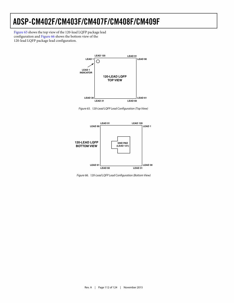
Rev. A | Page 112 of 124 | November 2015
ADSP-CM402F/CM403F/CM407F/CM408F/CM409FFigure 65 shows the top view of the 120-lead LQFP package lead configuration and Figure 66 shows the bottom view of the 120-lead LQFP package lead configuration.
Figure 65. 120-Lead LQFP Lead Configuration (Top View)
Figure 66. 120-Lead LQFP Lead Configuration (Bottom View)
LEAD 1
LEAD 120
LEAD 30LEAD 31
LEAD 91LEAD 90
LEAD 60LEAD 61
LEAD 1INDICATOR
120-LEAD LQFPTOP VIEW
LEAD 90LEAD 91
LEAD 61LEAD 60
LEAD 120LEAD 1
LEAD 31LEAD 30
120-LEAD LQFPBOTTOM VIEW
GND PAD(LEAD 121)
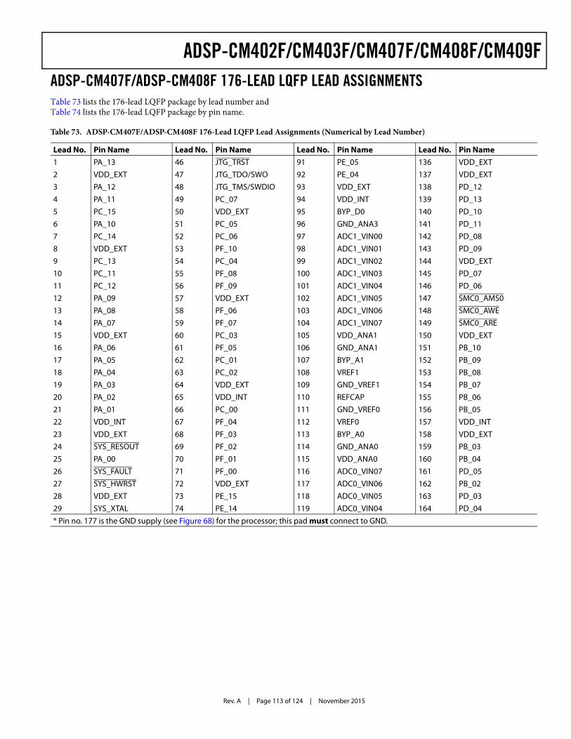
Rev. A | Page 113 of 124 | November 2015
ADSP-CM402F/CM403F/CM407F/CM408F/CM409FADSP-CM407F/ADSP-CM408F 176-LEAD LQFP LEAD ASSIGNMENTSTable 73 lists the 176-lead LQFP package by lead number and Table 74 lists the 176-lead LQFP package by pin name.
Table 73. ADSP-CM407F/ADSP-CM408F 176-Lead LQFP Lead Assignments (Numerical by Lead Number)
Lead No. Pin Name Lead No. Pin Name Lead No. Pin Name Lead No. Pin Name1 PA_13 46 JTG_TRST 91 PE_05 136 VDD_EXT2 VDD_EXT 47 JTG_TDO/SWO 92 PE_04 137 VDD_EXT3 PA_12 48 JTG_TMS/SWDIO 93 VDD_EXT 138 PD_124 PA_11 49 PC_07 94 VDD_INT 139 PD_135 PC_15 50 VDD_EXT 95 BYP_D0 140 PD_106 PA_10 51 PC_05 96 GND_ANA3 141 PD_117 PC_14 52 PC_06 97 ADC1_VIN00 142 PD_088 VDD_EXT 53 PF_10 98 ADC1_VIN01 143 PD_099 PC_13 54 PC_04 99 ADC1_VIN02 144 VDD_EXT10 PC_11 55 PF_08 100 ADC1_VIN03 145 PD_0711 PC_12 56 PF_09 101 ADC1_VIN04 146 PD_0612 PA_09 57 VDD_EXT 102 ADC1_VIN05 147 SMC0_AMS013 PA_08 58 PF_06 103 ADC1_VIN06 148 SMC0_AWE14 PA_07 59 PF_07 104 ADC1_VIN07 149 SMC0_ARE15 VDD_EXT 60 PC_03 105 VDD_ANA1 150 VDD_EXT16 PA_06 61 PF_05 106 GND_ANA1 151 PB_1017 PA_05 62 PC_01 107 BYP_A1 152 PB_0918 PA_04 63 PC_02 108 VREF1 153 PB_0819 PA_03 64 VDD_EXT 109 GND_VREF1 154 PB_0720 PA_02 65 VDD_INT 110 REFCAP 155 PB_0621 PA_01 66 PC_00 111 GND_VREF0 156 PB_0522 VDD_INT 67 PF_04 112 VREF0 157 VDD_INT23 VDD_EXT 68 PF_03 113 BYP_A0 158 VDD_EXT24 SYS_RESOUT 69 PF_02 114 GND_ANA0 159 PB_0325 PA_00 70 PF_01 115 VDD_ANA0 160 PB_0426 SYS_FAULT 71 PF_00 116 ADC0_VIN07 161 PD_0527 SYS_HWRST 72 VDD_EXT 117 ADC0_VIN06 162 PB_0228 VDD_EXT 73 PE_15 118 ADC0_VIN05 163 PD_0329 SYS_XTAL 74 PE_14 119 ADC0_VIN04 164 PD_04* Pin no. 177 is the GND supply (see Figure 68) for the processor; this pad must connect to GND.
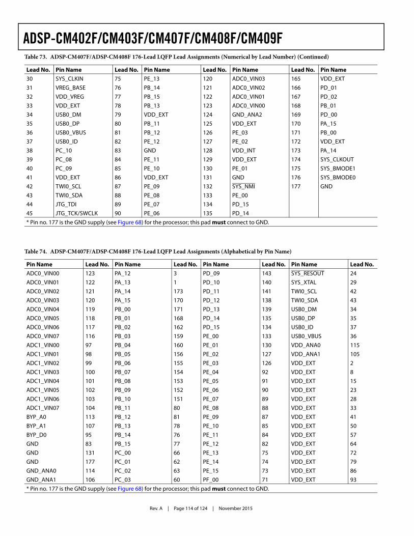
Rev. A | Page 114 of 124 | November 2015
ADSP-CM402F/CM403F/CM407F/CM408F/CM409F
30 SYS_CLKIN 75 PE_13 120 ADC0_VIN03 165 VDD_EXT31 VREG_BASE 76 PB_14 121 ADC0_VIN02 166 PD_0132 VDD_VREG 77 PB_15 122 ADC0_VIN01 167 PD_0233 VDD_EXT 78 PB_13 123 ADC0_VIN00 168 PB_0134 USB0_DM 79 VDD_EXT 124 GND_ANA2 169 PD_0035 USB0_DP 80 PB_11 125 VDD_EXT 170 PA_1536 USB0_VBUS 81 PB_12 126 PE_03 171 PB_0037 USB0_ID 82 PE_12 127 PE_02 172 VDD_EXT38 PC_10 83 GND 128 VDD_INT 173 PA_1439 PC_08 84 PE_11 129 VDD_EXT 174 SYS_CLKOUT40 PC_09 85 PE_10 130 PE_01 175 SYS_BMODE141 VDD_EXT 86 VDD_EXT 131 GND 176 SYS_BMODE042 TWI0_SCL 87 PE_09 132 SYS_NMI 177 GND43 TWI0_SDA 88 PE_08 133 PE_0044 JTG_TDI 89 PE_07 134 PD_1545 JTG_TCK/SWCLK 90 PE_06 135 PD_14
Table 73. ADSP-CM407F/ADSP-CM408F 176-Lead LQFP Lead Assignments (Numerical by Lead Number) (Continued)
Lead No. Pin Name Lead No. Pin Name Lead No. Pin Name Lead No. Pin Name
* Pin no. 177 is the GND supply (see Figure 68) for the processor; this pad must connect to GND.
Table 74. ADSP-CM407F/ADSP-CM408F 176-Lead LQFP Lead Assignments (Alphabetical by Pin Name)
Pin Name Lead No. Pin Name Lead No. Pin Name Lead No. Pin Name Lead No.ADC0_VIN00 123 PA_12 3 PD_09 143 SYS_RESOUT 24ADC0_VIN01 122 PA_13 1 PD_10 140 SYS_XTAL 29ADC0_VIN02 121 PA_14 173 PD_11 141 TWI0_SCL 42ADC0_VIN03 120 PA_15 170 PD_12 138 TWI0_SDA 43ADC0_VIN04 119 PB_00 171 PD_13 139 USB0_DM 34ADC0_VIN05 118 PB_01 168 PD_14 135 USB0_DP 35ADC0_VIN06 117 PB_02 162 PD_15 134 USB0_ID 37ADC0_VIN07 116 PB_03 159 PE_00 133 USB0_VBUS 36ADC1_VIN00 97 PB_04 160 PE_01 130 VDD_ANA0 115ADC1_VIN01 98 PB_05 156 PE_02 127 VDD_ANA1 105ADC1_VIN02 99 PB_06 155 PE_03 126 VDD_EXT 2ADC1_VIN03 100 PB_07 154 PE_04 92 VDD_EXT 8ADC1_VIN04 101 PB_08 153 PE_05 91 VDD_EXT 15ADC1_VIN05 102 PB_09 152 PE_06 90 VDD_EXT 23ADC1_VIN06 103 PB_10 151 PE_07 89 VDD_EXT 28ADC1_VIN07 104 PB_11 80 PE_08 88 VDD_EXT 33BYP_A0 113 PB_12 81 PE_09 87 VDD_EXT 41BYP_A1 107 PB_13 78 PE_10 85 VDD_EXT 50BYP_D0 95 PB_14 76 PE_11 84 VDD_EXT 57GND 83 PB_15 77 PE_12 82 VDD_EXT 64GND 131 PC_00 66 PE_13 75 VDD_EXT 72GND 177 PC_01 62 PE_14 74 VDD_EXT 79GND_ANA0 114 PC_02 63 PE_15 73 VDD_EXT 86GND_ANA1 106 PC_03 60 PF_00 71 VDD_EXT 93* Pin no. 177 is the GND supply (see Figure 68) for the processor; this pad must connect to GND.
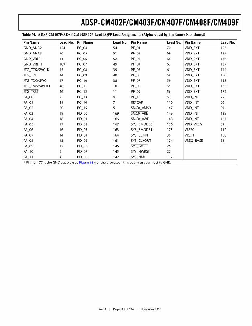
Rev. A | Page 115 of 124 | November 2015
ADSP-CM402F/CM403F/CM407F/CM408F/CM409F
GND_ANA2 124 PC_04 54 PF_01 70 VDD_EXT 125GND_ANA3 96 PC_05 51 PF_02 69 VDD_EXT 129GND_VREF0 111 PC_06 52 PF_03 68 VDD_EXT 136GND_VREF1 109 PC_07 49 PF_04 67 VDD_EXT 137JTG_TCK/SWCLK 45 PC_08 39 PF_05 61 VDD_EXT 144JTG_TDI 44 PC_09 40 PF_06 58 VDD_EXT 150JTG_TDO/SWO 47 PC_10 38 PF_07 59 VDD_EXT 158JTG_TMS/SWDIO 48 PC_11 10 PF_08 55 VDD_EXT 165JTG_TRST 46 PC_12 11 PF_09 56 VDD_EXT 172PA_00 25 PC_13 9 PF_10 53 VDD_INT 22PA_01 21 PC_14 7 REFCAP 110 VDD_INT 65PA_02 20 PC_15 5 SMC0_AMS0 147 VDD_INT 94PA_03 19 PD_00 169 SMC0_ARE 149 VDD_INT 128PA_04 18 PD_01 166 SMC0_AWE 148 VDD_INT 157PA_05 17 PD_02 167 SYS_BMODE0 176 VDD_VREG 32PA_06 16 PD_03 163 SYS_BMODE1 175 VREF0 112PA_07 14 PD_04 164 SYS_CLKIN 30 VREF1 108PA_08 13 PD_05 161 SYS_CLKOUT 174 VREG_BASE 31PA_09 12 PD_06 146 SYS_FAULT 26PA_10 6 PD_07 145 SYS_HWRST 27PA_11 4 PD_08 142 SYS_NMI 132
Table 74. ADSP-CM407F/ADSP-CM408F 176-Lead LQFP Lead Assignments (Alphabetical by Pin Name) (Continued)
Pin Name Lead No. Pin Name Lead No. Pin Name Lead No. Pin Name Lead No.
* Pin no. 177 is the GND supply (see Figure 68) for the processor; this pad must connect to GND.
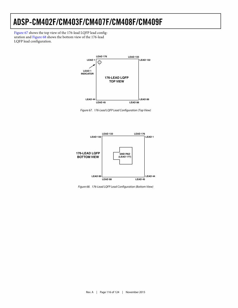
Rev. A | Page 116 of 124 | November 2015
ADSP-CM402F/CM403F/CM407F/CM408F/CM409FFigure 67 shows the top view of the 176-lead LQFP lead config-uration and Figure 68 shows the bottom view of the 176-lead LQFP lead configuration.
Figure 67. 176-Lead LQFP Lead Configuration (Top View)
LEAD 1
LEAD 176
LEAD 44LEAD 45
LEAD 133LEAD 132
LEAD 88LEAD 89
LEAD 1INDICATOR
176-LEAD LQFPTOP VIEW
Figure 68. 176-Lead LQFP Lead Configuration (Bottom View)
LEAD 132LEAD 133
LEAD 89LEAD 88
LEAD 176LEAD 1
LEAD 45LEAD 44
176-LEAD LQFPBOTTOM VIEW
GND PAD(LEAD 177)
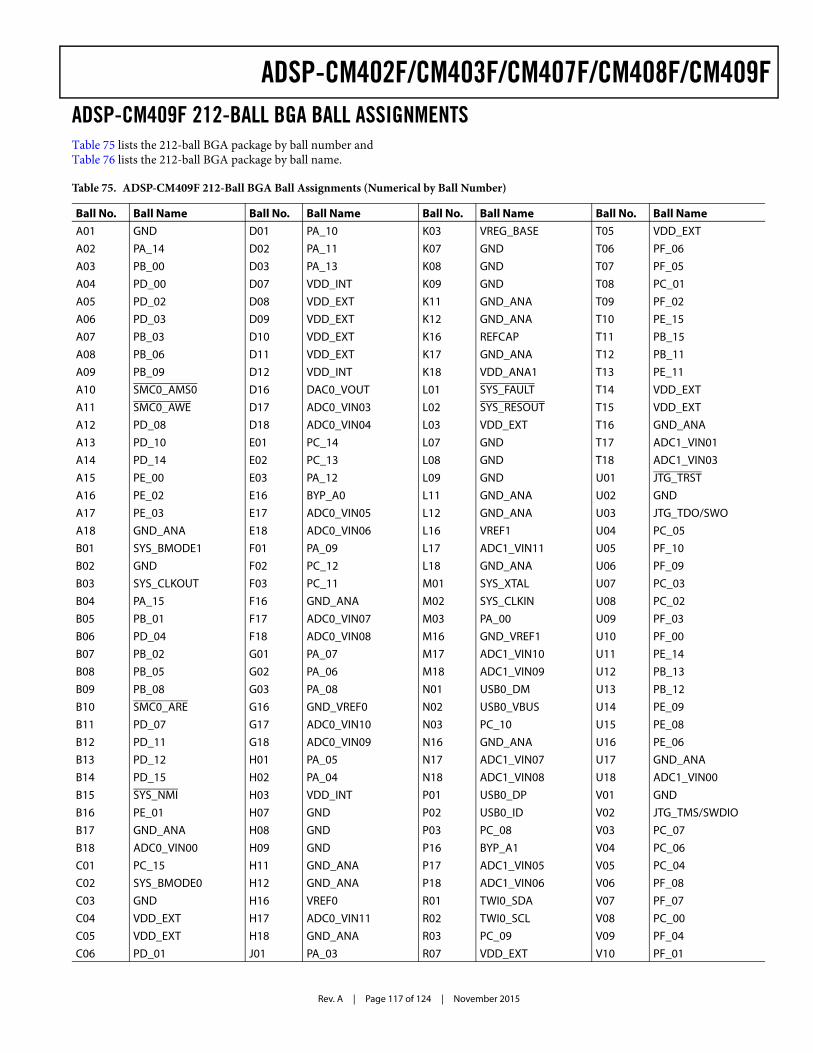
Rev. A | Page 117 of 124 | November 2015
ADSP-CM402F/CM403F/CM407F/CM408F/CM409FADSP-CM409F 212-BALL BGA BALL ASSIGNMENTSTable 75 lists the 212-ball BGA package by ball number and Table 76 lists the 212-ball BGA package by ball name.
Table 75. ADSP-CM409F 212-Ball BGA Ball Assignments (Numerical by Ball Number)
Ball No. Ball Name Ball No. Ball Name Ball No. Ball Name Ball No. Ball NameA01 GND D01 PA_10 K03 VREG_BASE T05 VDD_EXTA02 PA_14 D02 PA_11 K07 GND T06 PF_06A03 PB_00 D03 PA_13 K08 GND T07 PF_05A04 PD_00 D07 VDD_INT K09 GND T08 PC_01A05 PD_02 D08 VDD_EXT K11 GND_ANA T09 PF_02A06 PD_03 D09 VDD_EXT K12 GND_ANA T10 PE_15A07 PB_03 D10 VDD_EXT K16 REFCAP T11 PB_15A08 PB_06 D11 VDD_EXT K17 GND_ANA T12 PB_11A09 PB_09 D12 VDD_INT K18 VDD_ANA1 T13 PE_11A10 SMC0_AMS0 D16 DAC0_VOUT L01 SYS_FAULT T14 VDD_EXTA11 SMC0_AWE D17 ADC0_VIN03 L02 SYS_RESOUT T15 VDD_EXTA12 PD_08 D18 ADC0_VIN04 L03 VDD_EXT T16 GND_ANAA13 PD_10 E01 PC_14 L07 GND T17 ADC1_VIN01A14 PD_14 E02 PC_13 L08 GND T18 ADC1_VIN03A15 PE_00 E03 PA_12 L09 GND U01 JTG_TRSTA16 PE_02 E16 BYP_A0 L11 GND_ANA U02 GNDA17 PE_03 E17 ADC0_VIN05 L12 GND_ANA U03 JTG_TDO/SWOA18 GND_ANA E18 ADC0_VIN06 L16 VREF1 U04 PC_05B01 SYS_BMODE1 F01 PA_09 L17 ADC1_VIN11 U05 PF_10B02 GND F02 PC_12 L18 GND_ANA U06 PF_09B03 SYS_CLKOUT F03 PC_11 M01 SYS_XTAL U07 PC_03B04 PA_15 F16 GND_ANA M02 SYS_CLKIN U08 PC_02B05 PB_01 F17 ADC0_VIN07 M03 PA_00 U09 PF_03B06 PD_04 F18 ADC0_VIN08 M16 GND_VREF1 U10 PF_00B07 PB_02 G01 PA_07 M17 ADC1_VIN10 U11 PE_14B08 PB_05 G02 PA_06 M18 ADC1_VIN09 U12 PB_13B09 PB_08 G03 PA_08 N01 USB0_DM U13 PB_12B10 SMC0_ARE G16 GND_VREF0 N02 USB0_VBUS U14 PE_09B11 PD_07 G17 ADC0_VIN10 N03 PC_10 U15 PE_08B12 PD_11 G18 ADC0_VIN09 N16 GND_ANA U16 PE_06B13 PD_12 H01 PA_05 N17 ADC1_VIN07 U17 GND_ANAB14 PD_15 H02 PA_04 N18 ADC1_VIN08 U18 ADC1_VIN00B15 SYS_NMI H03 VDD_INT P01 USB0_DP V01 GNDB16 PE_01 H07 GND P02 USB0_ID V02 JTG_TMS/SWDIOB17 GND_ANA H08 GND P03 PC_08 V03 PC_07B18 ADC0_VIN00 H09 GND P16 BYP_A1 V04 PC_06C01 PC_15 H11 GND_ANA P17 ADC1_VIN05 V05 PC_04C02 SYS_BMODE0 H12 GND_ANA P18 ADC1_VIN06 V06 PF_08C03 GND H16 VREF0 R01 TWI0_SDA V07 PF_07C04 VDD_EXT H17 ADC0_VIN11 R02 TWI0_SCL V08 PC_00C05 VDD_EXT H18 GND_ANA R03 PC_09 V09 PF_04C06 PD_01 J01 PA_03 R07 VDD_EXT V10 PF_01
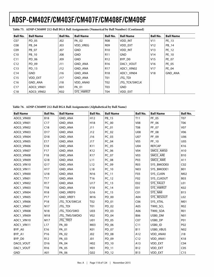
Rev. A | Page 118 of 124 | November 2015
ADSP-CM402F/CM403F/CM407F/CM408F/CM409F
C07 PD_05 J02 PA_02 R08 VDD_INT V11 PE_13C08 PB_04 J03 VDD_VREG R09 VDD_EXT V12 PB_14C09 PB_07 J07 GND R10 VDD_INT V13 PE_12C10 PB_10 J08 GND R11 GND V14 PE_10C11 PD_06 J09 GND R12 BYP_D0 V15 PE_07C12 PD_09 J11 GND_ANA R16 DAC1_VOUT V16 PE_05C13 PD_13 J12 GND_ANA R17 ADC1_VIN02 V17 PE_04C14 GND J16 GND_ANA R18 ADC1_VIN04 V18 GND_ANAC15 VDD_EXT J17 GND_ANA T01 JTG_TDIC16 GND_ANA J18 VDD_ANA0 T02 JTG_TCK/SWCLKC17 ADC0_VIN01 K01 PA_01 T03 GNDC18 ADC0_VIN02 K02 SYS_HWRST T04 VDD_EXT
Table 75. ADSP-CM409F 212-Ball BGA Ball Assignments (Numerical by Ball Number) (Continued)
Ball No. Ball Name Ball No. Ball Name Ball No. Ball Name Ball No. Ball Name
Table 76. ADSP-CM409F 212-Ball BGA Ball Assignments (Alphabetical by Ball Name)
Ball Name Ball No. Ball Name Ball No. Ball Name Ball No. Ball Name Ball No.ADC0_VIN00 B18 GND_ANA H12 PB_15 T11 PF_05 T07ADC0_VIN01 C17 GND_ANA H18 PC_00 V08 PF_06 T06ADC0_VIN02 C18 GND_ANA J11 PC_01 T08 PF_07 V07ADC0_VIN03 D17 GND_ANA J12 PC_02 U08 PF_08 V06ADC0_VIN04 D18 GND_ANA J16 PC_03 U07 PF_09 U06ADC0_VIN05 E17 GND_ANA J17 PC_04 V05 PF_10 U05ADC0_VIN06 E18 GND_ANA K11 PC_05 U04 REFCAP K16ADC0_VIN07 F17 GND_ANA K12 PC_06 V04 SMC0_AMS0 A10ADC0_VIN08 F18 GND_ANA K17 PC_07 V03 SMC0_ARE B10ADC0_VIN09 G18 GND_ANA L11 PC_08 P03 SMC0_AWE A11ADC0_VIN10 G17 GND_ANA L12 PC_09 R03 SYS_BMODE0 C02ADC0_VIN11 H17 GND_ANA L18 PC_10 N03 SYS_BMODE1 B01ADC1_VIN00 U18 GND_ANA N16 PC_11 F03 SYS_CLKIN M02ADC1_VIN01 T17 GND_ANA T16 PC_12 F02 SYS_CLKOUT B03ADC1_VIN02 R17 GND_ANA U17 PC_13 E02 SYS_FAULT L01ADC1_VIN03 T18 GND_ANA V18 PC_14 E01 SYS_HWRST K02ADC1_VIN04 R18 GND_VREF0 G16 PC_15 C01 SYS_NMI B15ADC1_VIN05 P17 GND_VREF1 M16 PD_00 A04 SYS_RESOUT L02ADC1_VIN06 P18 JTG_TCK/SWCLK T02 PD_01 C06 SYS_XTAL M01ADC1_VIN07 N17 JTG_TDI T01 PD_02 A05 TWI0_SCL R02ADC1_VIN08 N18 JTG_TDO/SWO U03 PD_03 A06 TWI0_SDA R01ADC1_VIN09 M18 JTG_TMS/SWDIO V02 PD_04 B06 USB0_DM N01ADC1_VIN10 M17 JTG_TRST U01 PD_05 C07 USB0_DP P01ADC1_VIN11 L17 PA_00 M03 PD_06 C11 USB0_ID P02BYP_A0 E16 PA_01 K01 PD_07 B11 USB0_VBUS N02BYP_A1 P16 PA_02 J02 PD_08 A12 VDD_ANA0 J18BYP_D0 R12 PA_03 J01 PD_09 C12 VDD_ANA1 K18DAC0_VOUT D16 PA_04 H02 PD_10 A13 VDD_EXT C04DAC1_VOUT R16 PA_05 H01 PD_11 B12 VDD_EXT C05GND A01 PA_06 G02 PD_12 B13 VDD_EXT C15
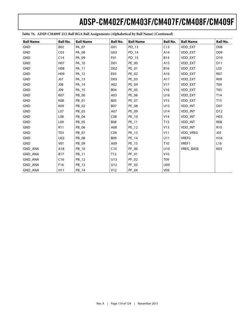
Rev. A | Page 119 of 124 | November 2015
ADSP-CM402F/CM403F/CM407F/CM408F/CM409F
GND B02 PA_07 G01 PD_13 C13 VDD_EXT D08GND C03 PA_08 G03 PD_14 A14 VDD_EXT D09GND C14 PA_09 F01 PD_15 B14 VDD_EXT D10GND H07 PA_10 D01 PE_00 A15 VDD_EXT D11GND H08 PA_11 D02 PE_01 B16 VDD_EXT L03GND H09 PA_12 E03 PE_02 A16 VDD_EXT R07GND J07 PA_13 D03 PE_03 A17 VDD_EXT R09GND J08 PA_14 A02 PE_04 V17 VDD_EXT T04GND J09 PA_15 B04 PE_05 V16 VDD_EXT T05GND K07 PB_00 A03 PE_06 U16 VDD_EXT T14GND K08 PB_01 B05 PE_07 V15 VDD_EXT T15GND K09 PB_02 B07 PE_08 U15 VDD_INT D07GND L07 PB_03 A07 PE_09 U14 VDD_INT D12GND L08 PB_04 C08 PE_10 V14 VDD_INT H03GND L09 PB_05 B08 PE_11 T13 VDD_INT R08GND R11 PB_06 A08 PE_12 V13 VDD_INT R10GND T03 PB_07 C09 PE_13 V11 VDD_VREG J03GND U02 PB_08 B09 PE_14 U11 VREF0 H16GND V01 PB_09 A09 PE_15 T10 VREF1 L16GND_ANA A18 PB_10 C10 PF_00 U10 VREG_BASE K03GND_ANA B17 PB_11 T12 PF_01 V10GND_ANA C16 PB_12 U13 PF_02 T09GND_ANA F16 PB_13 U12 PF_03 U09GND_ANA H11 PB_14 V12 PF_04 V09
Table 76. ADSP-CM409F 212-Ball BGA Ball Assignments (Alphabetical by Ball Name) (Continued)
Ball Name Ball No. Ball Name Ball No. Ball Name Ball No. Ball Name Ball No.
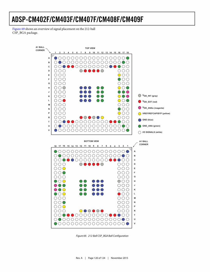
Rev. A | Page 120 of 124 | November 2015
ADSP-CM402F/CM403F/CM407F/CM408F/CM409FFigure 69 shows an overview of signal placement on the 212-ball CSP_BGA package.
Figure 69. 212-Ball CSP_BGA Ball Configuration
9 108 11 12 13 14 15 16 17 1875 642 31
BOTTOM VIEW
A
B
C
D
E
F
G
H
J
K
L
M
N
P
R
T
U
V
A1 BALLCORNER
TOP VIEW
VDD_ANAx (magenta)
VDD_EXT (red)
VDD_INT (gray)
GND_ANA (green)
VREF/REFCAP/BYP (yellow)
GND (blue)
I/O SIGNALS (white)
A
B
C
D
E
F
G
H
J
K
L
M
N
P
R
T
U
V
910 81112131415161718 7 56 4 23 1
A1 BALLCORNER
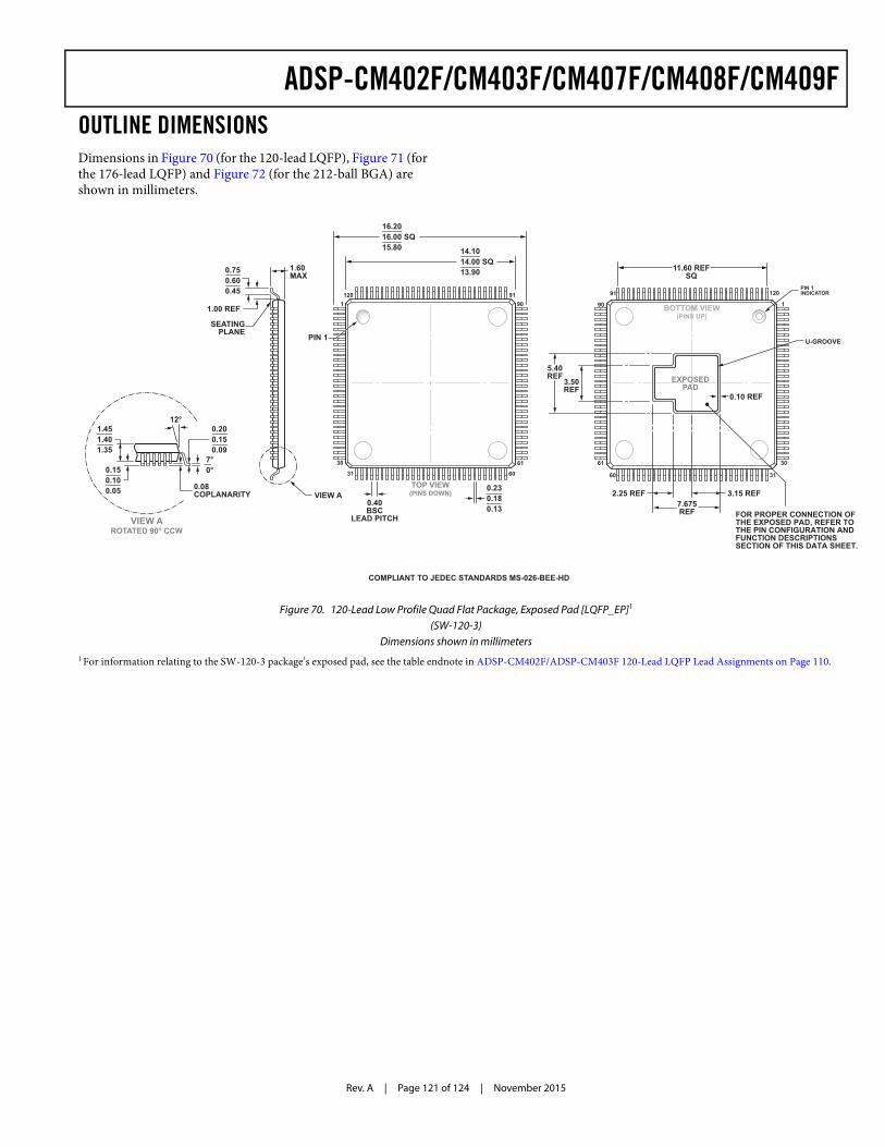
Rev. A | Page 121 of 124 | November 2015
ADSP-CM402F/CM403F/CM407F/CM408F/CM409FOUTLINE DIMENSIONSDimensions in Figure 70 (for the 120-lead LQFP), Figure 71 (for the 176-lead LQFP) and Figure 72 (for the 212-ball BGA) are shown in millimeters.
Figure 70. 120-Lead Low Profile Quad Flat Package, Exposed Pad [LQFP_EP]1
(SW-120-3)Dimensions shown in millimeters
1 For information relating to the SW-120-3 package’s exposed pad, see the table endnote in ADSP-CM402F/ADSP-CM403F 120-Lead LQFP Lead Assignments on Page 110.
120
60
90
61
31
1
30
91
COMPLIANT TO JEDEC STANDARDS MS-026-BEE-HD
1.451.401.35
0.150.100.05
TOP VIEW(PINS DOWN)
911 90
31
30
60
61
120
0.230.180.13
0.40BSC
LEAD PITCH
11.60 REFSQ
1.60MAX
16.2016.00 SQ15.80 14.10
14.00 SQ13.90
VIEW A 0.08COPLANARITY
VIEW A ROTATED 90° CCW
12°
7°0°
0.200.150.09
0.750.600.45
1.00 REF
EXPOSEDPAD
5.40REF
7.675REF
3.50REF
0.10 REF
U-GROOVE
2.25 REF 3.15 REF
FOR PROPER CONNECTION OF THE EXPOSED PAD, REFER TO THE PIN CONFIGURATION AND FUNCTION DESCRIPTIONS SECTION OF THIS DATA SHEET.
PIN 1SEATING
PLANE
PIN 1INDICATOR
BOTTOM VIEW(PINS UP)
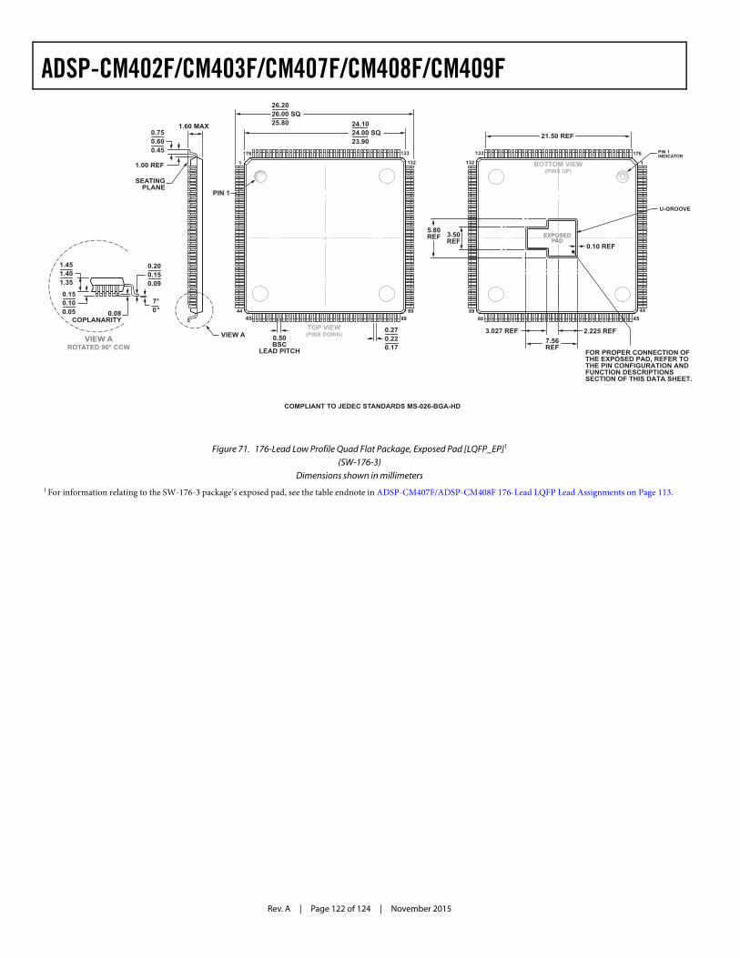
Rev. A | Page 122 of 124 | November 2015
ADSP-CM402F/CM403F/CM407F/CM408F/CM409F
Figure 71. 176-Lead Low Profile Quad Flat Package, Exposed Pad [LQFP_EP]1
(SW-176-3)Dimensions shown in millimeters
1 For information relating to the SW-176-3 package’s exposed pad, see the table endnote in ADSP-CM407F/ADSP-CM408F 176-Lead LQFP Lead Assignments on Page 113.
COMPLIANT TO JEDEC STANDARDS MS-026-BGA-HD
0.150.100.05 0.08
COPLANARITY
0.200.150.09
1.451.401.35
7°0°
VIEW A ROTATED 90° CCW
0.270.220.17
0.750.600.45
0.50BSC
LEAD PITCH
24.1024.00 SQ23.90
26.2026.00 SQ25.80
1
44
1
4445
8988 4588
132
89
132
176 133 176133
1.60 MAX
1.00 REF
SEATINGPLANE
VIEW A
5.80REF
7.56REF
3.50REF
3.027 REF 2.225 REF
21.50 REF
FOR PROPER CONNECTION OF THE EXPOSED PAD, REFER TO THE PIN CONFIGURATION AND FUNCTION DESCRIPTIONS SECTION OF THIS DATA SHEET.
0.10 REF
U-GROOVE
BOTTOM VIEW(PINS UP)
EXPOSEDPAD
TOP VIEW(PINS DOWN)
PIN 1
PIN 1INDICATOR
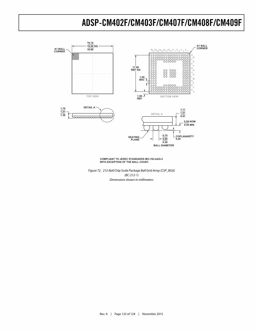
Rev. A | Page 123 of 124 | November 2015
ADSP-CM402F/CM403F/CM407F/CM408F/CM409F
Figure 72. 212-Ball Chip Scale Package Ball Grid Array [CSP_BGA](BC-212-1)
Dimensions shown in millimeters
1.00BSC
17.00REF SQ
19.1019.00 SQ18.90
COMPLIANT TO JEDEC STANDARDS MO-192-AAG-2WITH EXCEPTION OF THE BALL COUNT.
1.00REF
AB
CD
EF
G
910 81112131415161718 7 56 4 23 1
BOTTOM VIEW
HJ
KL
MN
PR
TU
V
DETAIL A
TOP VIEW
DETAIL A
COPLANARITY0.20
0.700.600.50
BALL DIAMETER
SEATINGPLANE
A1 BALLCORNER
A1 BALLCORNER
1.111.010.91
1.701.511.36
0.50 NOM0.45 MIN
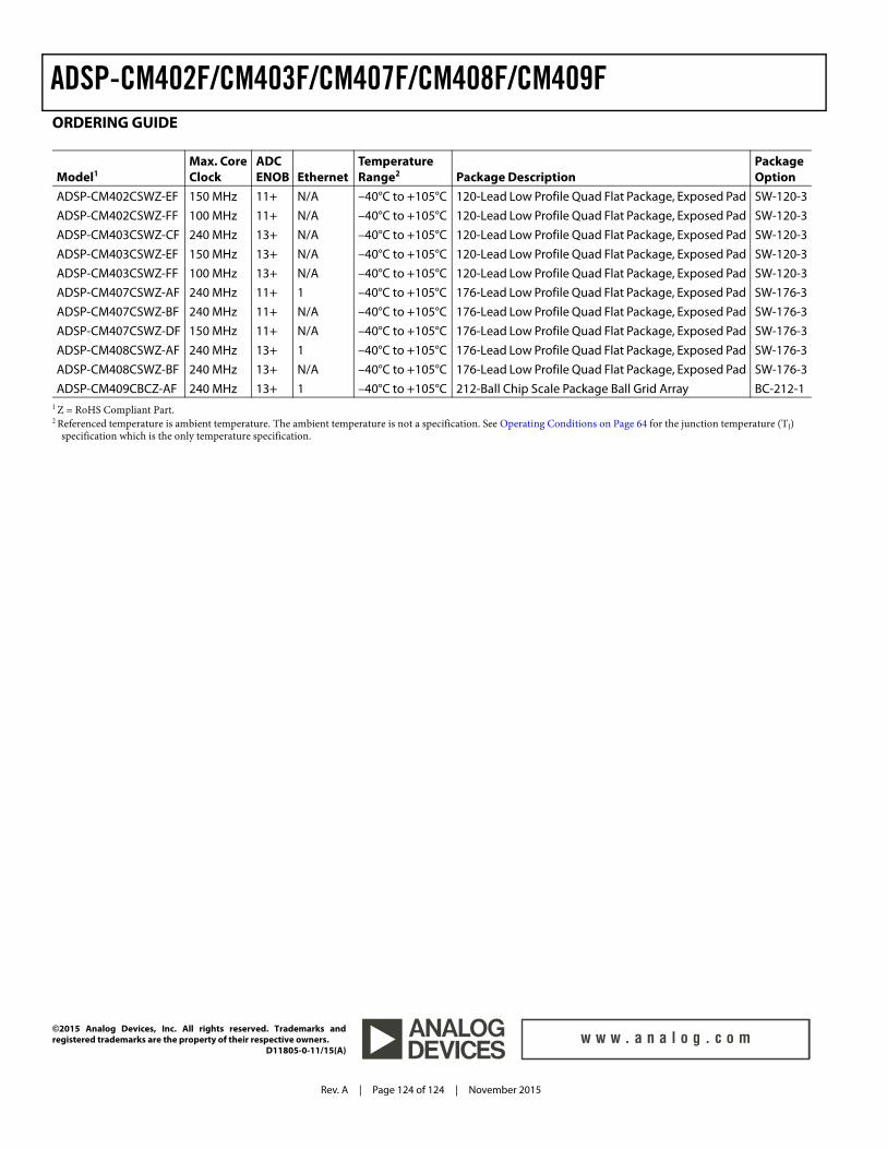
Rev. A | Page 124 of 124 | November 2015
©2015 Analog Devices, Inc. All rights reserved. Trademarks andregistered trademarks are the property of their respective owners.
D11805-0-11/15(A)
ADSP-CM402F/CM403F/CM407F/CM408F/CM409FORDERING GUIDE
Model1
1 Z = RoHS Compliant Part.
Max. CoreClock
ADC ENOB Ethernet
TemperatureRange2
2 Referenced temperature is ambient temperature. The ambient temperature is not a specification. See Operating Conditions on Page 64 for the junction temperature (TJ) specification which is the only temperature specification.
Package DescriptionPackageOption
ADSP-CM402CSWZ-EF 150 MHz 11+ N/A –40°C to +105°C 120-Lead Low Profile Quad Flat Package, Exposed Pad SW-120-3ADSP-CM402CSWZ-FF 100 MHz 11+ N/A –40°C to +105°C 120-Lead Low Profile Quad Flat Package, Exposed Pad SW-120-3ADSP-CM403CSWZ-CF 240 MHz 13+ N/A –40°C to +105°C 120-Lead Low Profile Quad Flat Package, Exposed Pad SW-120-3ADSP-CM403CSWZ-EF 150 MHz 13+ N/A –40°C to +105°C 120-Lead Low Profile Quad Flat Package, Exposed Pad SW-120-3ADSP-CM403CSWZ-FF 100 MHz 13+ N/A –40°C to +105°C 120-Lead Low Profile Quad Flat Package, Exposed Pad SW-120-3ADSP-CM407CSWZ-AF 240 MHz 11+ 1 –40°C to +105°C 176-Lead Low Profile Quad Flat Package, Exposed Pad SW-176-3ADSP-CM407CSWZ-BF 240 MHz 11+ N/A –40°C to +105°C 176-Lead Low Profile Quad Flat Package, Exposed Pad SW-176-3ADSP-CM407CSWZ-DF 150 MHz 11+ N/A –40°C to +105°C 176-Lead Low Profile Quad Flat Package, Exposed Pad SW-176-3ADSP-CM408CSWZ-AF 240 MHz 13+ 1 –40°C to +105°C 176-Lead Low Profile Quad Flat Package, Exposed Pad SW-176-3ADSP-CM408CSWZ-BF 240 MHz 13+ N/A –40°C to +105°C 176-Lead Low Profile Quad Flat Package, Exposed Pad SW-176-3ADSP-CM409CBCZ-AF 240 MHz 13+ 1 –40°C to +105°C 212-Ball Chip Scale Package Ball Grid Array BC-212-1