mm-wave telecommunication & big-data processing solutions...
TRANSCRIPT

1
www.multifractal.orgAll Rights Reserved.
©
Mm-wave telecommunication & big-data processing solutions
Technology overview
06 June 2017
2
www.multifractal.orgAll Rights Reserved.
©
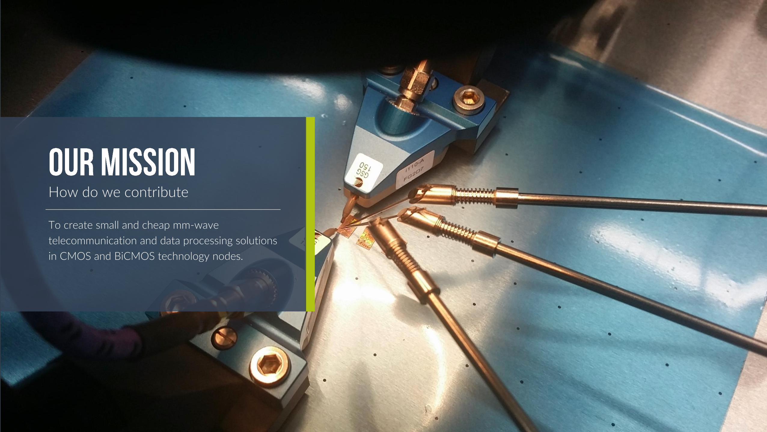
How do we contribute
To create small and cheap mm-wave
telecommunication and data processing solutions
in CMOS and BiCMOS technology nodes.

3
www.multifractal.orgAll Rights Reserved.
©
Miniaturization and full monolithic integration of
ultra high bandwidth wireless transceivers in
commercial silicon technologies:
Developing communications grade tunable mm-wave (Ka – W band) on-chip bandpass filters.1Developing ASP/DSP to process the high bandwidth signals (5 GHz for 5G).
Developing communications grade amplifiers such as LNAs and PAs.
2
3
4 Developing other front-end components such as oscillators, mixers, phase shifters and antenna.

4
www.multifractal.orgAll Rights Reserved.
©
Silicon basedSince our systems are silicon
based they are cheaper,
offer full analogue/digital
integration and have a large
manufacturing capacity
worldwide.
Skilled teamOur expertise and skilled
team in bleeding-edge mm-
wave telecommunication IC
sub-systems gives us the
rare ability to design other
such systems to stringent
customer requirements as
necessitated for future
wireless mm-wave systems.
Intellectual propertyMultifractal Semiconductors
will commercialize this
technology portfolio by
licencing it to integrated
device manufacturers (IDMs)
and fabless semiconductor
companies.
Multifractal has developed novel on-chip bandpass filters and digital signal processing (DSP) blocks as necessitated by future 5G technologies.
5
www.multifractal.orgAll Rights Reserved.
©
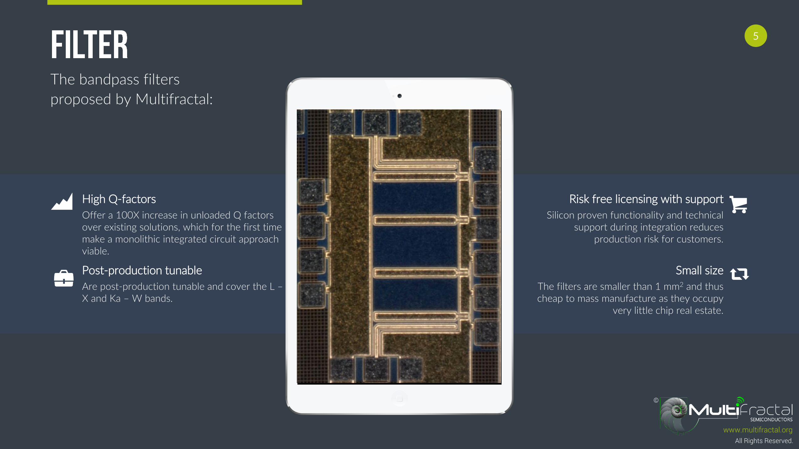
High Q-factors
Offer a 100X increase in unloaded Q factors over existing solutions, which for the first time make a monolithic integrated circuit approach viable.
Post-production tunable
Are post-production tunable and cover the L –X and Ka – W bands.
Risk free licensing with support
Silicon proven functionality and technical support during integration reduces
production risk for customers.
Small size
The filters are smaller than 1 mm2 and thus cheap to mass manufacture as they occupy
very little chip real estate.
The bandpass filters
proposed by Multifractal:

6
www.multifractal.orgAll Rights Reserved.
©
High speed
Boast multi-gigahertz bandwidths (speeds 30X higher (5000X under certain conditions) than SOTA).
Paradigm shift
Rely on an analogue internal mode of operation (paradigm shift – big data problem).
Low power
Boast power consumptions 40x lower to existing SOTA DSPs.
Small size
The ASPs are smaller than 4 mm2 and thus cheap to mass manufacture as they occupy
very little chip real estate.
The first ever, specialised
set of (A)DSPs have been
developed by Multifractal,
which:

7
www.multifractal.orgAll Rights Reserved.
©
Mm-wave telecommunication & big data
processing solutions.
8
www.multifractal.orgAll Rights Reserved.
©
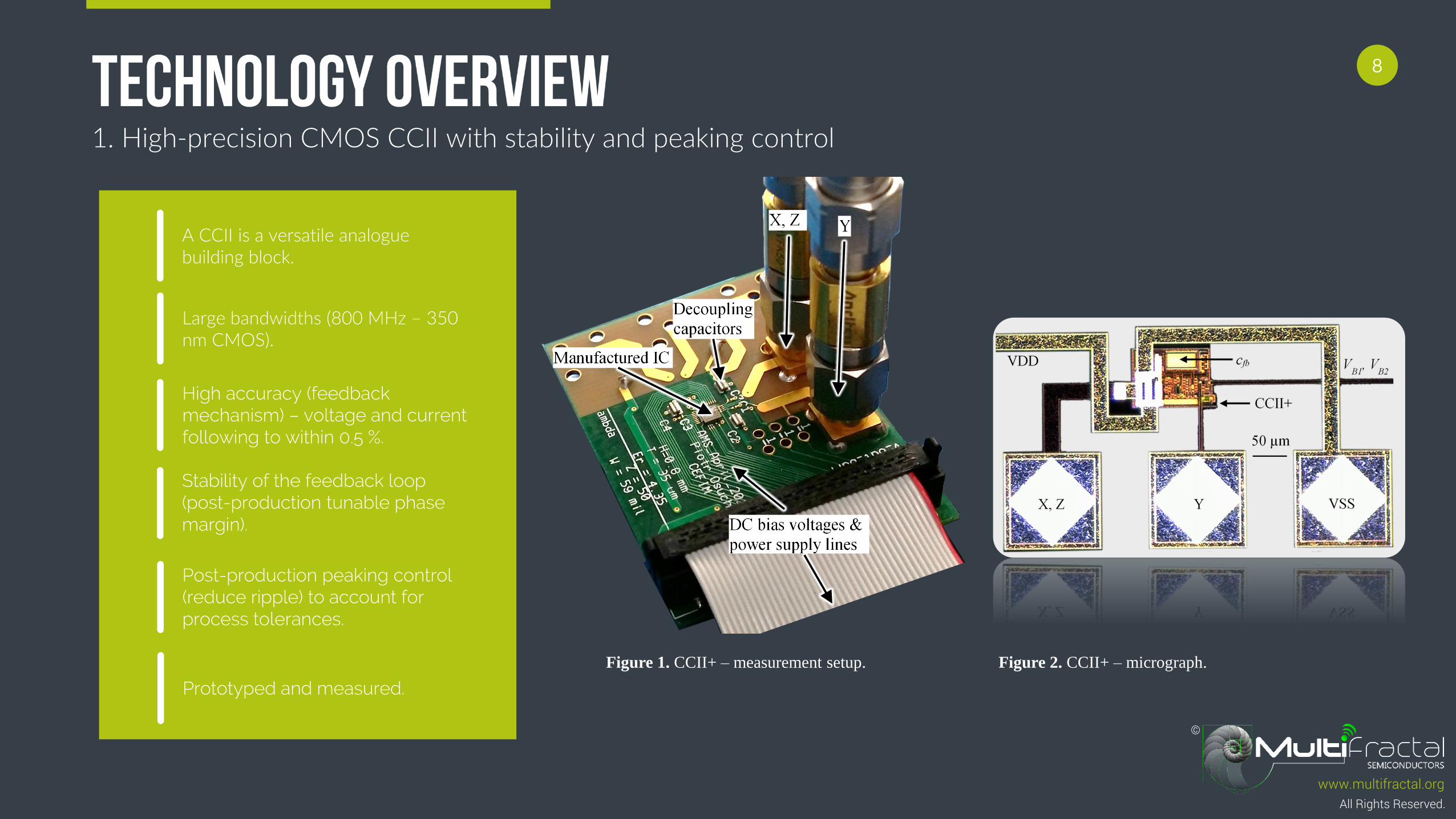
Large bandwidths (800 MHz – 350 nm CMOS).
High accuracy (feedback mechanism) – voltage and current following to within 0.5 %.
Stability of the feedback loop (post-production tunable phase margin).
Post-production peaking control (reduce ripple) to account for process tolerances.
1. High-precision CMOS CCII with stability and peaking control
Figure 1. CCII+ – measurement setup. Figure 2. CCII+ – micrograph.
A CCII is a versatile analogue building block.
Prototyped and measured.

9
www.multifractal.orgAll Rights Reserved.
©
A second-order all-pass network is the fundamental building block of any analogue signal processor (ASP).
Traditionally bulky soft-substrate passive microstrip solutions are used.
First-ever active on-chip second-order all-pass network.
Low insertion loss ripple ( < 1 dB),occupies 0.0625 mm2 real-estate,frequency agile in all two degrees of freedom, reduced sensitivity to process tolerances, based on the CCII.
2. Tunable active second-order all-pass network (CMOS)
Figure 5. Second-order all-pass network – micrograph.
100 microns
Prototyped and measured.
10
www.multifractal.orgAll Rights Reserved.
©
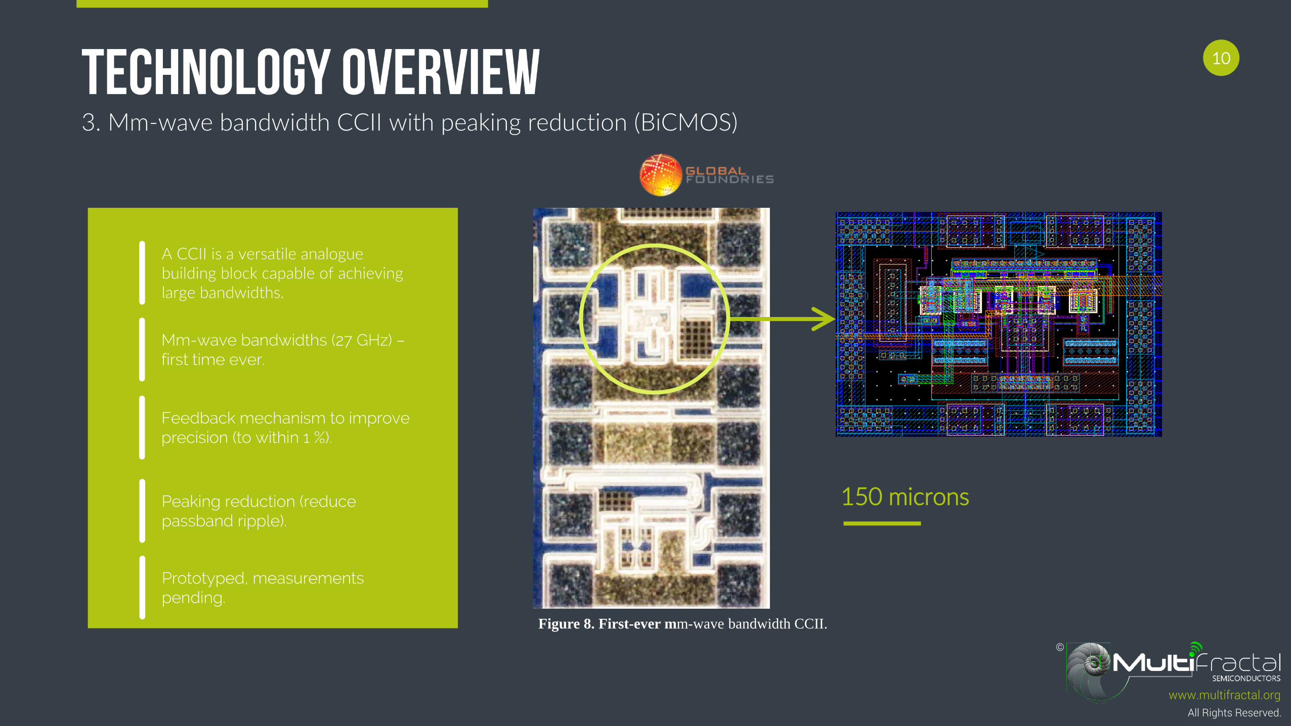
A CCII is a versatile analogue building block capable of achieving large bandwidths.
Mm-wave bandwidths (27 GHz) –first time ever.
Feedback mechanism to improve precision (to within 1 %).
Peaking reduction (reduce passband ripple).
3. Mm-wave bandwidth CCII with peaking reduction (BiCMOS)
Figure 8. First-ever mm-wave bandwidth CCII.
150 microns
Prototyped, measurements pending.
11
www.multifractal.orgAll Rights Reserved.
©
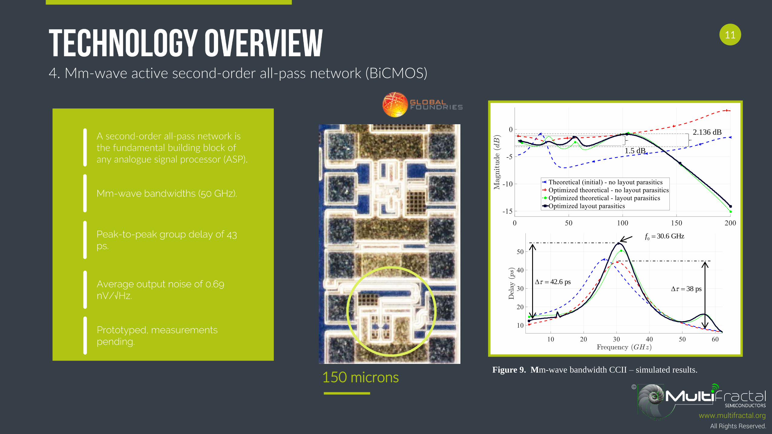
A second-order all-pass network is the fundamental building block of any analogue signal processor (ASP).
Mm-wave bandwidths (50 GHz).
Peak-to-peak group delay of 43 ps.
Average output noise of 0.69 nV/√Hz.
4. Mm-wave active second-order all-pass network (BiCMOS)
Figure 9. Mm-wave bandwidth CCII – simulated results.150 microns
42.6 ps
0 30.6 GHzf
38 ps
2.136 dB
1.5 dB
Prototyped, measurements pending.
12
www.multifractal.orgAll Rights Reserved.
©
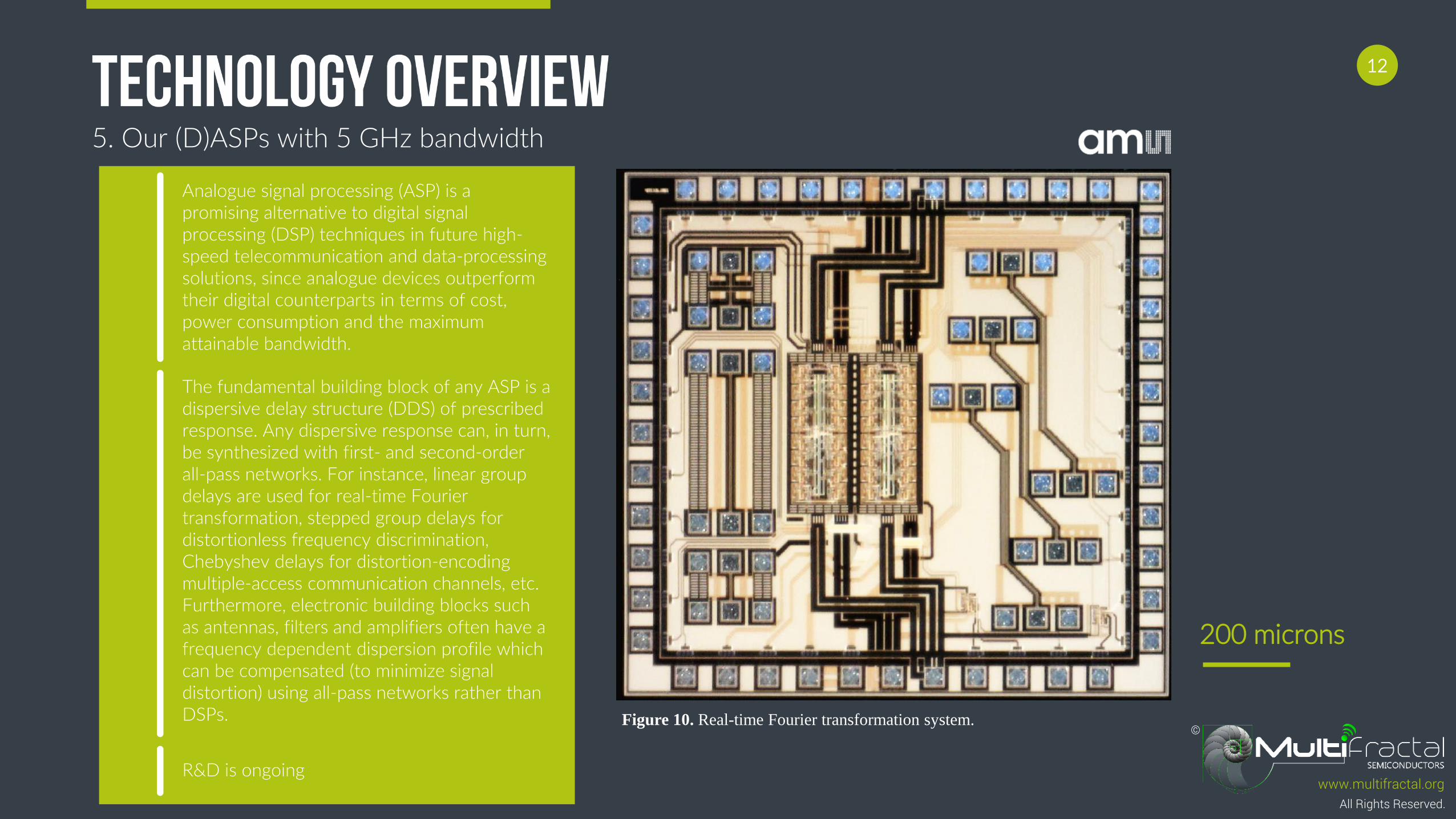
Analogue signal processing (ASP) is a promising alternative to digital signal processing (DSP) techniques in future high-speed telecommunication and data-processing solutions, since analogue devices outperform their digital counterparts in terms of cost, power consumption and the maximum attainable bandwidth.
5. Our (D)ASPs with 5 GHz bandwidth
Figure 10. Real-time Fourier transformation system.
200 microns
The fundamental building block of any ASP is a dispersive delay structure (DDS) of prescribed response. Any dispersive response can, in turn, be synthesized with first- and second-order all-pass networks. For instance, linear group delays are used for real-time Fourier transformation, stepped group delays for distortionless frequency discrimination, Chebyshev delays for distortion-encoding multiple-access communication channels, etc. Furthermore, electronic building blocks such as antennas, filters and amplifiers often have a frequency dependent dispersion profile which can be compensated (to minimize signal distortion) using all-pass networks rather than DSPs.
R&D is ongoing

13
www.multifractal.orgAll Rights Reserved.
©
SOTA Q0 of ≈10, Our Q0 of ≈1000.
SiGe BiCMOS processes.
E-band (71-76 and 81-86 GHz.
Centre frequency and Q-factor tunable with control voltages.
6. Fully tunable, active, enhanced, high Q-factor mm-wave resonators
Figure 11. Simulation results of the tunable, high-Q mm-wave resonators.

14
www.multifractal.orgAll Rights Reserved.
©
Fractional bandwidths of 0.5%.
Filters as narrow as 500 MHz.
Applicable to E-Band 71-76 and 81-86 GHz.
Resonator Q0 enhanced from 10 to 1000.
7. Narrowband coupled resonator bandpass filters
Figure 12. Simulation results of the tunable, high-Q mm-wave resonators.
300 microns
15
www.multifractal.orgAll Rights Reserved.
©
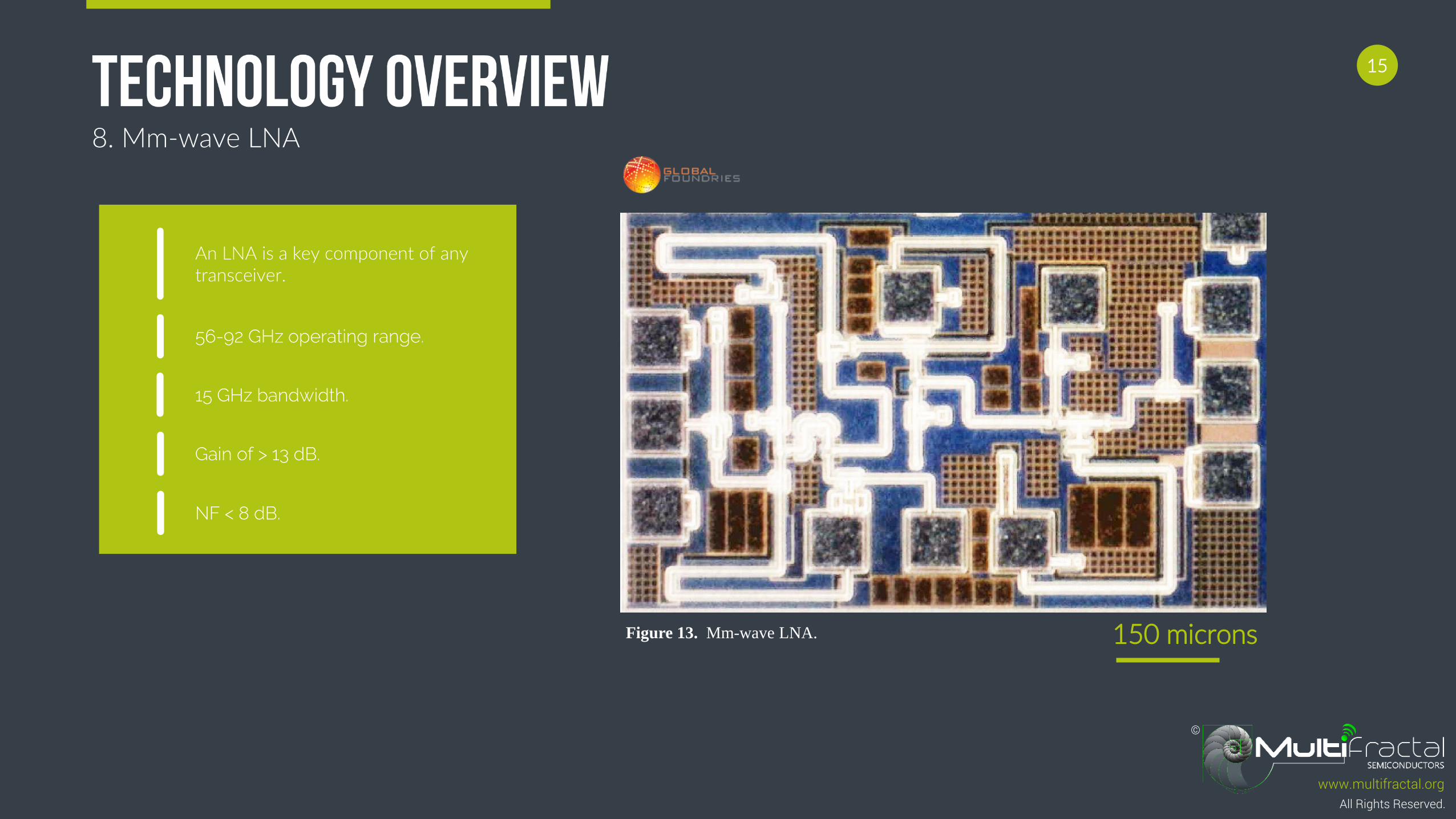
An LNA is a key component of any transceiver.
56-92 GHz operating range.
8. Mm-wave LNA
Figure 13. Mm-wave LNA.
15 GHz bandwidth.
Gain of > 13 dB.
NF < 8 dB.
150 microns

16
www.multifractal.orgAll Rights Reserved.
©
What we prototype and what we license
R & D Licensing
17
www.multifractal.orgAll Rights Reserved.
©
We look forward to forming a partnership
Pretoria, South Africa
Nish: [email protected]: [email protected]
Nish: +27 723452957
Address
Contact Info
Telephone
All Rights Reserved.
©
www.multifractal.org
twitter.com/multifractal_sa