model-driven physical-design for future nanoscale architectures
TRANSCRIPT

Model-Driven Physical-Design for Future Nanoscale Architectures
Ciprian TEODOROV
Lab-STICC MOCS
November, 28th 2011

Generic physical-design framework
based on a common vocabulary
is the key to taming
nanoscale architectures.
Thesis statement

Context
• Smaller & denser circuits which consume much less power
Society Needs
• Current technology (CMOS) reaches its limits
However
• Different architectural propositions based on emergent technologies
State of the art
Model-Driven Physical-Design for Future Nanoscale Architectures
3

Examples
Quantum
• quantum-dot cellular automata
Molecular
• Tour’s Nanocell
Crossbar
• NanoPLA, CMOL, NASIC, FPNI
Model-Driven Physical-Design for Future Nanoscale Architectures
4

What is a Crossbar ?
CrosspointDifferent devices: • Diode• FET• Etc.
Model-Driven Physical-Design for Future Nanoscale Architectures
5
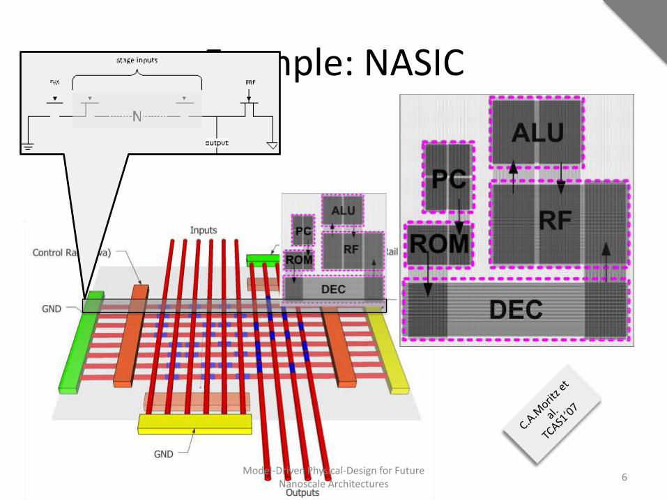
Example: NASICutilization and performance.
5. NASIC Architectures Large scale computing systems may be designed using the NASIC fabric and the associated
framework of building blocks, xnwFET based circuits, and logic styles discussed in the
preceding sections. This section discusses two key architectures for the NASIC fabric: the WISP-
0 general purpose processor and a massively parallel architectural framework with
programmable templates for image processing.
5.1 WIre Streaming Processor (WISP-0)
WISP-0 is a stream processor that implements a 5-stage
microprocessor pipeline architecture including fetch,
decode, register file, execute and write back stages.
WISP-0 consists of five nanotiles: Program Counter (PC),
ROM, Decoder (DEC), Register File (RF) and Arithmetic
Logic Unit (ALU). Figure 17 shows its layout. A nanotile
is shown as a box surrounded by dashed lines in the
figure. In WISP designs, in order to preserve the density
advantages of nanodevices, data is streamed through the
fabric with minimal control/feedback paths. All hazards
are exposed to the compiler. It uses dynamic circuits and
pipelining on the wires to eliminate the need for explicit
flip-flops and therefore improve the density considerably.
WISP-0 supports a simple instruction set including nop,
mov, movi, add and multiply functions. It uses a 7-bit
instruction format with 3-bit instruction and 2-bit source
and destination addresses. The WISP-0 is used as a design
prototype for evaluating key metrics such as area and
performance as well as the impact of various fault-
tolerance techniques on chip yield and process variation
mitigation. Additional enhancements to this design are
ongoing in the NASIC group.
5.1.1 WISP-0 Program Counter
The WISP-0 program counter is implemented as a four bit accumulator. Its output is a four bit
address that acts as an input to the ROM. The address is incremented each cycle and fed back
using a nano-latch. Figure 18 shows the implementation of the Program Counter with a NAND-
NAND scheme. Diagonal transistors on the upper two NAND planes implement the nano-latch
to delay the output by one cycle and allow the signals to ‘turn the corner’.
Figure 18. WISP-0 Program Counter
Figure 17. WISP-0 Processor Floorplan
Model-Driven Physical-Design for Future Nanoscale Architectures
6

Common Features of Crossbar Fabrics
Nanowire based
Regularity of assembly leads to:
• a crossbar-like structure
• PLA and/or FPGA-like fabric architecture
CMOS superstructure, thus a nano-CMOS interface
Large number of defects
Logic implementation
Model-Driven Physical-Design for Future Nanoscale Architectures
7

Differences Between Crossbar Fabrics
Architectural differences
• Nano-role, CMOS-role
• Fabrication strategy
Physical parameters used for evaluation
• CMOS/NW pitch / device characteristics
Evaluation strategies
• Yield simulation
• Place & Route on predefined array
Hypotheses during evaluation
• Defect/Faults models
Model-Driven Physical-Design for Future Nanoscale Architectures
8

Research Questions
How to maximize the reuse of design-tools?
Is it possible to create a generic design toolkit?
How to separate the algorithmic and architectural concerns?
How to add a tools axis to design-space exploration problem?
How to integrate multi-level fault tolerance?
Model-Driven Physical-Design for Future Nanoscale Architectures
9

Contributions
Model-driven physical-design @ nanoscale
Common vocabulary
Tools as model transformation
Reified design flow
DSE bootstrap methodology
R2D NASIC: Nanoscale
architecturetemplate
Max-rate pipeline routing
Model-Driven Physical-Design for Future Nanoscale Architectures
10

Outline
MoNaDe Toolkit
•Overview
•Structural Domain Modeling
•Tool Modeling
•Design flow Modeling
R2D NASIC
•Overview
•Analytic evaluation
•Characteristics
R2D NASIC Evaluation Results
•Surface / Performance
•Max-rate pipeline evaluation
•Room for improvements
Conclusion & Perspectives
Model-Driven Physical-Design for Future Nanoscale Architectures
11

Outline
MoNaDe Toolkit
•Overview
•Structural Domain Modeling
•Tool Modeling
•Design flow Modeling
R2D NASIC
•Overview
•Analytic evaluation
•Characteristics
R2D NASIC Evaluation Results
•Surface / Performance
•Max-rate pipeline evaluation
•Room for improvements
Conclusion & Perspectives
Model-Driven Physical-Design for Future Nanoscale Architectures
12

System
RTL
Circuit
Fabric
Device
Model-Driven Physical-Design for Future Nanoscale Architectures
13

Typical Toolkit
Model-Driven Physical-Design for Future Nanoscale Architectures
14
Defect/Faults Application
Architecture ToolsPacking
Placement
Routing
UI
P&R OutputMetrics
MoNaDe

Structural Domain Modeling
Common abstract model
• Hierarchical annotated port graph
• Specialized to model applications and architectures
• Provides a common vocabulary (Entities and API)
• Enables the creation of generic utilities
Model-Driven Physical-Design for Future Nanoscale Architectures
15
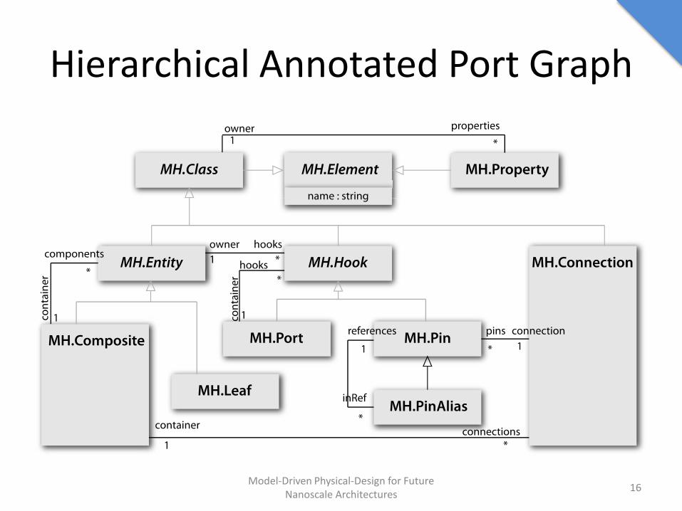
Hierarchical Annotated Port Graph
Model-Driven Physical-Design for Future Nanoscale Architectures
16

Structural Modeling:NASIC case
Model-Driven Physical-Design for Future Nanoscale Architectures
17

Model-Driven Physical-Design for Future Nanoscale Architectures
18

Structural Modeling:NanoPLA
Model-Driven Physical-Design for Future Nanoscale Architectures
19

Tools as Transformations
Decouple the algorithms from the domain models
The tools are implemented as composite model-to-model transformations
The tools refine the domain models
Integration of external tools and algorithms
Model-Driven Physical-Design for Future Nanoscale Architectures
20

Transformation Meta-Model
Model-Driven Physical-Design for Future Nanoscale Architectures
21
Model-Driven Physical-Design for Future Nanoscale Architectures
22
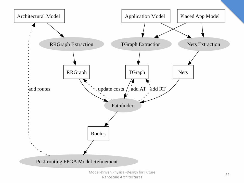
Architectural Model
RRGraph Extraction
Application Model
Nets ExtractionTGraph Extraction
Placed App Model
Nets
Pathfinder
RRGraph
Post-routing FPGA Model Refinement
TGraph
add AT add RTupdate costs
Routes
add routes

Tool-Flow Modeling
Reified tool-flow as a composite transformation
The physical-design tool-flow is a DAG of tools
Capacity to create tool-flow derivations
Enables incremental tool-flow creation
Enables Architecture/Tools exploration
Model-Driven Physical-Design for Future Nanoscale Architectures
23

Tool-Flow Hierarchy Example
Model-Driven Physical-Design for Future Nanoscale Architectures
24
SimpleDirectedAlongRoutePathEqFlow
NCellBasedSynthesis
VPRBasedFlow
LagrangianTimingDrivenFlow
DirectPlaceRouteDirectedConnections
VPRDirectPlaceAndRoute
DirectPlaceRoute
LagrangianPathEqualisationFlow
NAbstractFlow
CompleteArrayDirectPR
SimpleDirectedFSSwitchPathEqFlow
NFlowBasedSynthesis
MadeoBasedFlow
SimpleFSwitchPathEqualisationFlow
BASELINE
MAX-RATE
Outline
MoNaDe Toolkit
•Overview
•Structural Domain Modeling
•Tool Modeling
•Design flow Modeling
R2D NASIC
•Overview
•Analytic evaluation
•Characteristics
R2D NASIC Evaluation Results
•Surface / Performance
•Max-rate pipeline evaluation
•Room for improvements
Conclusion & Perspectives
Model-Driven Physical-Design for Future Nanoscale Architectures
25

NASIC 2D Routing Problem
Model-Driven Physical-Design for Future Nanoscale Architectures
26

Model-Driven Physical-Design for Future Nanoscale Architectures
27

R2D NASIC – Routing & Timing
Model-Driven Physical-Design for Future Nanoscale Architectures
28

Results – NW Length
Model-Driven Physical-Design for Future Nanoscale Architectures
29

Performance vs Input width
0,00E+00
2,00E+08
4,00E+08
6,00E+08
8,00E+08
1,00E+09
1,20E+09
1,40E+09
1,60E+09
1,80E+09
1 3 5 7 9111315171921232527293133353739414345474951535557596163656769
Frequency(Hz)
#ofinputs
Model-Driven Physical-Design for Future Nanoscale Architectures
30
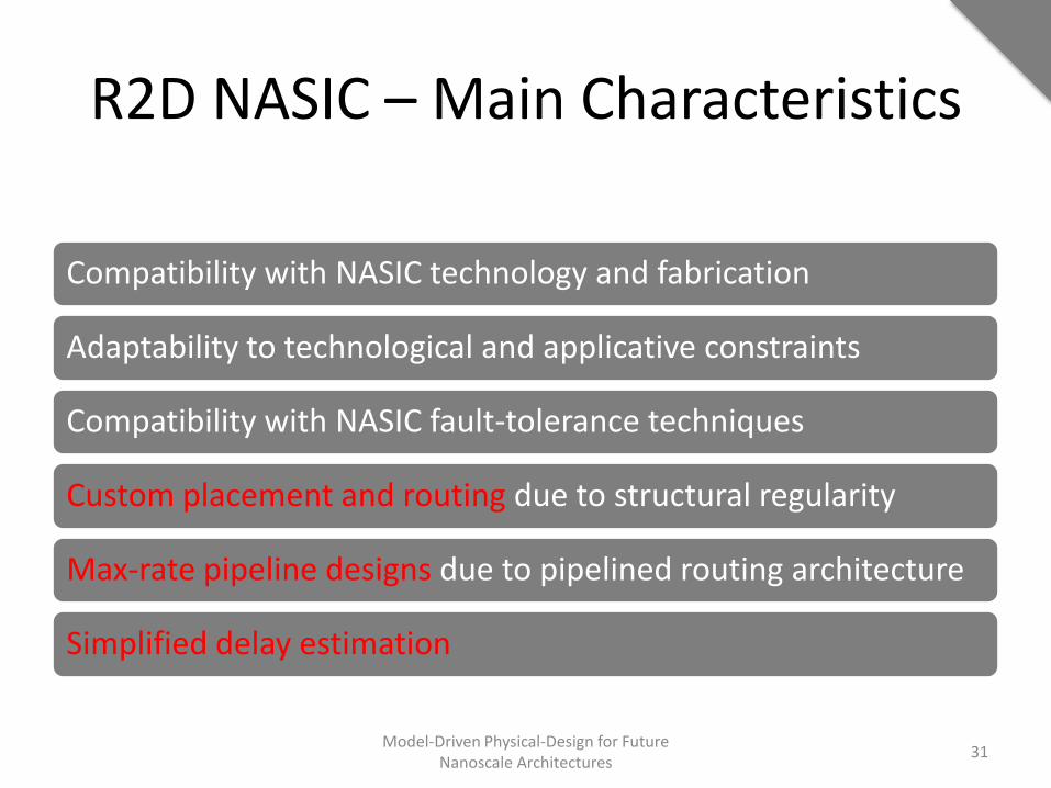
R2D NASIC – Main Characteristics
Compatibility with NASIC technology and fabrication
Adaptability to technological and applicative constraints
Compatibility with NASIC fault-tolerance techniques
Custom placement and routing due to structural regularity
Max-rate pipeline designs due to pipelined routing architecture
Simplified delay estimation
Model-Driven Physical-Design for Future Nanoscale Architectures
31

Outline
MoNaDe Toolkit
•Overview
•Structural Domain Modeling
•Tool Modeling
•Design flow Modeling
R2D NASIC
•Overview
•Analytic evaluation
•Characteristics
R2D NASIC Evaluation Results
•Surface / Performance
•Max-rate pipeline evaluation
•Room for improvements
Conclusion & Perspectives
Model-Driven Physical-Design for Future Nanoscale Architectures
32

R2D NASIC Toolflow
Model-Driven Physical-Design for Future Nanoscale Architectures
33
Application
Architecture Tools PLAMap
Placement
RoutingUI
P&R OutputMetrics
MoNaDe
PLA Explore
SIS
UI

Normalized Density Gain over 45nm standard cell
17X
1.32X
48X
2X
24X
12X9X
1
10
100
alu4 apex2 apex4 des ex5p misex3 seq
Model-Driven Physical-Design for Future Nanoscale Architectures
34
BASELINE

Speed
43MHz67MHz
40MHz
9MHz
167MHz
29MHz 27MHz
1
10
100
1000
alu4 apex2 apex4 des ex5p misex3 seq
Frequency
Operating frequency of the slowest logic stage / throughput
Results assume 1GHz for the slowest logic stage
Too slow
Model-Driven Physical-Design for Future Nanoscale Architectures
35
BASELINE

Max-Rate Pipeline System
Add REs
Model-Driven Physical-Design for Future Nanoscale Architectures
36

Model-Driven Physical-Design for Future Nanoscale Architectures
37

R2D NASIC Toolflow
Model-Driven Physical-Design for Future Nanoscale Architectures
38
Application
Architecture Tools PLAMap
Placement
RoutingUI
P&R OutputMetrics
MoNaDe
PLA Explore
SIS
UI
Max-Rate Router

Net Performance Improvement
Model-Driven Physical-Design for Future Nanoscale Architectures
39
MAX-RATE

Normalized Density Gain over 45nm standard cell
17X
1.32X
48X
2X
24X
12X9X
3X
0.03X
12X
0.06X
13X
1.24X
0.46X
0.01
0.1
1
10
alu4 apex2 apex4 des ex5p misex3 seq
Baseline Max-Rate
Model-Driven Physical-Design for Future Nanoscale Architectures
40
MAX-RATE

Performance*Area Gain
66X
0.32X
274X
5X
61X40X
14X
0.1
1
10
100
1000
alu4 apex2 apex4 des ex5p misex3 seq
Model-Driven Physical-Design for Future Nanoscale Architectures
41
MAX-RATE

Room for Improvement: STDEV of Routing Block Usage
Model-Driven Physical-Design for Future Nanoscale Architectures
42
MAX-RATE

Outline
MoNaDe Toolkit
•Overview
•Structural Domain Modeling
•Tool Modeling
•Design flow Modeling
R2D NASIC
•Overview
•Analytic evaluation
•Characteristics
R2D NASIC Evaluation Results
•Surface / Performance
•Max-rate pipeline evaluation
•Room for improvements
Conclusion & Perspectives
Model-Driven Physical-Design for Future Nanoscale Architectures
43

Conclusions
Generic physical-design toolkit for nanoscale crossbar fabrics
• Model-driven approach: structure, algorithmics, and flow reified.
• Two main abstraction levels considered
• Quantitative incremental DSE, bootstrapped with standard tools + new exploration axis
Nanoscale architecture template
• Enables arbitrary routing for NASIC
• Shows the impact of pipelined (dynamic logic) routing
Model-Driven Physical-Design for Future Nanoscale Architectures
44

Future Research
MoNaDe toolkit
• Formalize the models and the API
• Hardware accelerated physical-design using external transformations
• Create an optimizing tool-flow execution engine
• Open infrastructure for architectural exploration in the context of new technologies
Nanoscale architectures @ techno level
• Fault tolerance for dynamic routing
• Parameter variability impact on multi-tile design
• Clock distribution in highly constrained 2D topologies
Nanoscale architecture @ design level
• Creation and/or improvement of pipeline aware tools (placement, routing, etc)
• Study the extent to which dynamic logic evaluation impacts the physical design for other architectures besides R2D NASIC
Model-Driven Physical-Design for Future Nanoscale Architectures
45

Model-Driven Physical-Design for Future Nanoscale Architectures
46

Configuration Management
Configuration types:
• Structural
• Fine-grain functional
• Coarse-grain functional
Configuration state-machine reified in the model
Different configuration policies
• One-time configuration
• Reconfiguration
Model-Driven Physical-Design for Future Nanoscale Architectures
47

Fault-Modeling and Injection
Domain concepts specialized to faulty entities
• FET -> StuckAt0FET and StuckAt1FET
Two ways to inject faults:
• Object swapping: injects faulty devices by replacing model instances
• Fault-configuration: uses a probabilistic configuration controller
Model-Driven Physical-Design for Future Nanoscale Architectures
48

Fault-Modeling and Injection - Details
Model-Driven Physical-Design for Future Nanoscale Architectures
49
NFET StuckAt1
StuckAt0
NULL
30%
NFET StuckAt1
StuckAt0
NULL30%
10%
60%